JP3707581B2 - Data processing system having self-aligned stack pointer and method thereof - Google Patents
Data processing system having self-aligned stack pointer and method thereofDownload PDFInfo
- Publication number
- JP3707581B2 JP3707581B2JP11344297AJP11344297AJP3707581B2JP 3707581 B2JP3707581 B2JP 3707581B2JP 11344297 AJP11344297 AJP 11344297AJP 11344297 AJP11344297 AJP 11344297AJP 3707581 B2JP3707581 B2JP 3707581B2
- Authority
- JP
- Japan
- Prior art keywords
- register
- value
- signal
- multiplexer
- exception
- Prior art date
- Legal status (The legal status is an assumption and is not a legal conclusion. Google has not performed a legal analysis and makes no representation as to the accuracy of the status listed.)
- Expired - Fee Related
Links
Images


Classifications
- G—PHYSICS
- G06—COMPUTING OR CALCULATING; COUNTING
- G06F—ELECTRIC DIGITAL DATA PROCESSING
- G06F13/00—Interconnection of, or transfer of information or other signals between, memories, input/output devices or central processing units
- G—PHYSICS
- G06—COMPUTING OR CALCULATING; COUNTING
- G06F—ELECTRIC DIGITAL DATA PROCESSING
- G06F9/00—Arrangements for program control, e.g. control units
- G06F9/06—Arrangements for program control, e.g. control units using stored programs, i.e. using an internal store of processing equipment to receive or retain programs
- G06F9/30—Arrangements for executing machine instructions, e.g. instruction decode
- G06F9/38—Concurrent instruction execution, e.g. pipeline or look ahead
- G06F9/3802—Instruction prefetching
- G06F9/3816—Instruction alignment, e.g. cache line crossing
- G—PHYSICS
- G06—COMPUTING OR CALCULATING; COUNTING
- G06F—ELECTRIC DIGITAL DATA PROCESSING
- G06F11/00—Error detection; Error correction; Monitoring
- G06F11/07—Responding to the occurrence of a fault, e.g. fault tolerance
- G06F11/0703—Error or fault processing not based on redundancy, i.e. by taking additional measures to deal with the error or fault not making use of redundancy in operation, in hardware, or in data representation
- G06F11/0706—Error or fault processing not based on redundancy, i.e. by taking additional measures to deal with the error or fault not making use of redundancy in operation, in hardware, or in data representation the processing taking place on a specific hardware platform or in a specific software environment
- G06F11/0721—Error or fault processing not based on redundancy, i.e. by taking additional measures to deal with the error or fault not making use of redundancy in operation, in hardware, or in data representation the processing taking place on a specific hardware platform or in a specific software environment within a central processing unit [CPU]
- G—PHYSICS
- G06—COMPUTING OR CALCULATING; COUNTING
- G06F—ELECTRIC DIGITAL DATA PROCESSING
- G06F11/00—Error detection; Error correction; Monitoring
- G06F11/07—Responding to the occurrence of a fault, e.g. fault tolerance
- G06F11/0703—Error or fault processing not based on redundancy, i.e. by taking additional measures to deal with the error or fault not making use of redundancy in operation, in hardware, or in data representation
- G06F11/0793—Remedial or corrective actions
- G—PHYSICS
- G06—COMPUTING OR CALCULATING; COUNTING
- G06F—ELECTRIC DIGITAL DATA PROCESSING
- G06F9/00—Arrangements for program control, e.g. control units
- G06F9/06—Arrangements for program control, e.g. control units using stored programs, i.e. using an internal store of processing equipment to receive or retain programs
- G06F9/30—Arrangements for executing machine instructions, e.g. instruction decode
- G06F9/38—Concurrent instruction execution, e.g. pipeline or look ahead
- G06F9/3861—Recovery, e.g. branch miss-prediction, exception handling
Landscapes
- Engineering & Computer Science (AREA)
- Theoretical Computer Science (AREA)
- Physics & Mathematics (AREA)
- General Engineering & Computer Science (AREA)
- General Physics & Mathematics (AREA)
- Software Systems (AREA)
- Quality & Reliability (AREA)
- Advance Control (AREA)
- Executing Machine-Instructions (AREA)
Description
Translated fromJapanese【0001】
【産業上の利用分野】
本発明は、一般にデータ処理システムに関し、さらに詳しくは、データ処理システム内のスタック・ポインタに関する。
【0002】
【従来の技術および発明が解決しようとする課題】
データ処理システムにおいては、スタック・ポインタはプログラム変数および一時的格納のメモリ位置を定義するメモリ・アドレス・ポインタとして通常用いられるハードウェア・レジスタである。従来、プログラミング・モデル内の1つ以上のレジスタが、システム・スタック・ポインタとしてハードウェアにより用いられる。多くのシステムでは、スタック・ポインタは、ある一定の動作の実行中に、命令集合により暗示的に用いられる。一般に、このアドレス・レジスタは、データをメモリ・スタック上に「押し出す」ことにより、関数間でオペランドを伝えることのできる現在のスタック・フレームの最上位を定義する。この押し出し動作は、スタック・ポインタを減分する段階と、次にこのデータを新しいスタック・ポインタ・アドレスにより定義される位置にコピーする段階とによって構成される。データがルーチンにより用いられた後で、スタック・ポインタを増分するだけでデータの割当が取り消され、前の値に戻る。この過程は、スタックの「ポッピング」と呼ばれる。
【0003】
一般に、これらのスタック・ポインタがメモリ・アドレスを定義するので、ユーザ・プログラムは、スタック最上位を定義するスタック・ポインタの内容を日常的に処理する。バイト,ワード,ロングワードなどの種々の寸法のオペランドがスタック上に押し出され、スタック最上位はいつでも任意の可能な整合(alignment) を指し示すことができる。任意のオペランド・アドレス整合に関して任意のオペランド寸法の自動的ハードウェア支援を行うプロセッサは、不整合に対応するといわれる。メモリ・アドレスがその本来の境界(boundary)に対応しない場合、オペランドは不整合状態(misalignment)にあるといわれる。本来の境界は、0−モジュロ−(オペランド寸法)のアドレスとして単純に定義される。たとえば、メモリ・バイト・アドレスが0−モジュロ−2の場合は、16ビット・ワードのオペランドが整合され、メモリ・バイト・アドレスが0−モジュロ−4の場合は32ビット・ロングワードが整合される。この定義に合わない整合は不整合オペランドとなる。
【0004】
多くのプロセッサは、種々の例外処理に対するハードウェア支援を備える。障害とも呼ばれる、これらの例外には、通常、割込,システム呼出および演算エラー条件が含まれる。その他の例外も起こることがある。一般に、例外が検出されると、プロセッサは障害時に装置のステータスを詳細に示す特殊な例外フレームを、システム・スタック最上位に作成する。この例外スタック・フレームが作成されると、プロセッサは例外の種類により特定される命令アドレスに制御を転送することにより、特別例外処理ルーチンに制御を渡す。一般に、例外処理ルーチンは、ある種の修正動作を開始することなどにより、障害を処理して、例外時に実行していたアプリケーションに戻る。
【0005】
多くのプロセッサは、ある種の特殊なエラー検出を採用して、他の例外処理の間に特定の破壊的障害条件が起こると、全体システム不良を生成して、プロセッサを停止させるだけにする。特定の境界におけるシステム・スタック・ポインタの整合は、この特殊な破壊的障害条件に含まれる。この確率を補償するために、従来技術によるシステムはいくつかの異なる解決法を実現してきたが、これらは大量のハードウェアを必要とする。たとえば、多くの従来技術による解決法は、オペランドが誤整合されないことを保障するハードウェア回路を必要とする。これらの解決法は、プロセッサの動作モードに基づいて複数のスタック・ポインタを組み込むのが普通である。この動作モードは、通常、実行プログラムに関する特権レベルを定義し、最も簡単な形では、2つのレベルの特権、すなわちスーパーバイザ(最高特権)とユーザ(最小特権)により構成されるのが普通である。スーパーバイザ・モードでの実行は、システムのすべての資源に対して完璧なアクセスが可能であり、ユーザ・モードの実行は、ある種のハードウェア資源に対するアクセスが拒否される。さらに、多くのプロセッサは、データ処理システム内のスタック・ポインタの必要な整合を強化するための専用ハードウェア回路構成を提供する。従来技術の解決法ではそれぞれ、専用ハードウェア回路構成とそれに相当する諸費用が必要となる点に留意すること。
【0006】
このような高価なハードウェア回路構成を組み込むことができないデータ処理システムのために、ソフトウェアによる解決法が開発されている。このようなソフトウェアによる解決法を用いる際は、同時発生する例外は許されない。言い換えると、データ処理システムにある例外が取り込まれると、他の例外は許されないということである。この場合、他の例外が隠され、アサートされると、装置状況のステータスおよびプログラム・カウンタ情報が更新される。かくして、データ処理システムは最初の例外が処理される前の状態に戻ることができなくなる。この第2番目の種類の従来技術のシステムでは、データ処理システムはすべての例外を正しく有効に処理することができない。
【0007】
現在ある従来の解決法は、例外がアサートされ処理された後で、データ処理システムを初期の状態に正しく回復するためには、大量の追加ハードウェア回路構成が必要になる。従って、データ処理システムの設計者がオペランドの誤整合(misalignment)に対するハードウェア支援を任意で備えることができ、しかもデータ処理システムがシステム・スタック・ポインタ整合に関わらずすべての例外を正しく処理して、例外処理の後で初期の状態を回復することができる解決法が必要である。
【0008】
【実施例】
本発明は、データ・プロセッサと、単独のシステム・スタック・ポインタを用いて、システム・スタックおよびユーザ・スタック・オペランドの整合に対するハードウェア支援が任意(optional)の場合に、システム・スタック動作およびユーザ・スタック動作の両方の記録を作成するデータ処理システムの動作方法とを提供する。この単独のシステム・スタック・ポインタは、自己整合スタック・ポインタとして実現される。簡単にいうと、この自己整合スタック・ポインタは現在のアドレス設定より低い、最も近い0−モジュロ−4アドレスに自身を自動的に整合して、誤整合されたオペランドに対してハードウェア支援がなくても整合システム・エラーが起こらないようにする。自動整合が行われると、本発明のデータ・プロセッサは、例外スタック・フレーム内に4ビット・フォーマット・フィールドを記憶し、障害時のスタック・ポインタの整合に関する情報を知らせる。例外が処理されて、例外からの復帰(RTE :return from exception )命令が実行されると、プロセッサは、例外スタック・フレームに記憶された4ビット・フォーマット・フィールドを用いて、スタック・ポインタを例外時の当初の値に回復する。
【0009】
本発明は、データ・プロセッサと、単独のスタック・ポインタを用いてデータ処理システムのスーパーバイザ・スタック・エリアおよびユーザ・スタック・エリアの両方を支援する動作方法とを提供する。さらに本発明においては、オペランドの誤整合専用のハードウェアを実現することもできるが、必須ではない。例外処理の間に、この単独のスタック・ポインタが自己整合を行うことができるので、データ・プロセッサは、スタック・ポインタの誤整合中に例外が起こっても、破滅的なエラーがデータ処理システムに起こらないようにすることができる。本発明の動作は、後で詳細に説明する。
【0010】
以下には、本発明を実現するデータ処理システムの構成と動作を詳細に述べる。
【0011】
以下の本発明の構成の説明においては、「バス」という用語は、データ,アドレス,制御またはステータスなど1つ以上の様々な種類の情報を転送するために用いられる複数の信号または導体を指す。「アサート」および「ネゲート」という用語は、信号,ステータス・ビットまたは同様の装置を論理的に真の状態、または論理的に偽の状態にすることをそれぞれ示す。論理的に真の状態が論理レベル1であれば、論理的に偽の状態は論理レベル0になる。論理的に真の状態が論理レベル0であれば、論理的に偽の状態は論理レベル0ということになる。
【0012】
さらに、数字の前に「$」という記号がつくと、その数値が16進数または基底16の形で表されることを示す。数字の前に「%」という記号がつくと、その数値が2進数(バイナリ値)または基底2の形で表されることを示す。
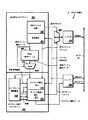
【0013】
ここで図1を参照して、図1は、本発明のある実施例によるデータ処理システム5を示す。データ処理システム5は、データ・プロセッサ3および外部開発システム7によって構成される。データ・プロセッサ3は、システム・バス・コントローラ8,プロセッサ・コア9,スレーブ・モジュール12,スレーブ・モジュール13,マスタ・モジュール14およびデバッグ・モジュール10を備える。システム・バス・コントローラ8は、E バスを介して外部装置(ここでは図示せず)に結合される。システム・バス・コントローラ8は、S バスを介してスレーブ・モジュール12およびスレーブ・モジュール13に結合される。S バスはスレーブ・モジュール・バスである。システム・バス・コントローラ8は、プロセッサ・コア9とマスタ・モジュール14とに、M バス23を介して結合される。M バス23はマスタ・モジュール・バスである。
【0014】
プロセッサ・コア9は、中央処理装置(CPU: central processing unit)2,メモリ管理ユニット(MMU: memory management unit )/コントローラ4およびメモリ6によって構成される。オペランド誤整合ユニット5は、プロセッサ・コア9に選択的に具備される。中央処理装置2,MMU /コントローラ4,メモリ6およびデバッグ・モジュール10はそれぞれ、K バス25を介して互いに結合される。中央処理装置2およびメモリ6も両方とも、MMU /コントローラ4にも直接的に接続される。MMU /コントローラ4は、M バス23を介してデータ処理システム5の残りの部分に情報を提供する。中央処理装置2は、デバッグ・モジュール10に結合され、内部制御バスを提供する。CPU 2は、外部装置(ここでは図示せず)からのリセット信号も受信する。デバッグ・モジュール10は、外部制御バスを用いて外部開発装置7と双方向に通信する。外部開発装置7は、データ処理システム5の外部にある任意の装置である。
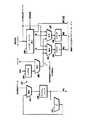
【0015】
図2は、CPU 2の部分をより詳細に図示する。CPU 2は、レジスタ208,命令取出パイプライン210,バッファ216,オペランド実行パイプライン220およびマルチプレクサ(MUX )222を備える。命令取出パイプライン210は、命令アドレス生成回路202,命令取出回路204,FIFO命令バッファ206およびマルチプレクサ219によって構成される。また、オペランド実行パイプライン220は、オペランド取出回路212,アドレス生成/実行回路214およびパイプライン制御論理218によって構成される。
【0016】
命令取出パイプライン210の命令アドレス生成回路202は、命令アドレス信号をマルチプレクサ222に提供する。マルチプレクサ222は、K バス25上でのその後のトランザクションのために、命令取出パイプライン210からの命令アドレスとオペランド実行パイプライン220からのオペランド・アドレスとの間で選択を行う。レジスタ208は、KADDR (K バス・アドレス)信号を出力する。命令取出パイプライン210の命令取出回路204は、オペランド取出回路212とバッファ216とに結合され、バッファリングされたKRDATA信号を受信する。命令取出回路204はオペランド取出回路212に結合され、命令取出アドレスを提供する。命令取出回路204は、FIFO命令バッファ206およびマルチプレクサ219にも結合され、命令バッファ書込データ信号を提供する。FIFO命令バッファ206は、マルチプレクサ219に結合され、命令バッファ読出データ信号を提供する。マルチプレクサ219は、オペランド実行パイプライン220のオペランド取出回路212に結合され、命令信号を提供する。
【0017】
オペランド実行パイプライン220のパイプライン制御論理218は、オペランド取出回路212に結合され、反転例外処理信号を提供する。パイプライン制御論理218は、アドレス生成/実行回路214にも結合され、制御バスを提供する。パイプライン制御論理218は、オペランド取出回路212とアドレス生成/実行回路214の両方に結合され、ベクトル信号を提供する。オペランド実行パイプライン220のアドレス生成/実行回路214は、マルチプレクサ222に結合され、オペランド・アドレス信号を提供する。同様に、アドレス生成/実行回路214は、バッファ216に結合され、オペランド書込データ信号を提供する。バッファ216は、KRDATA(K バス読出データ)信号とKWDATA(K バス書込データ)信号とを提供する。KRDATA,KWDATAおよびKADDR 信号は、それぞれK バス25に送られる。
【0018】
図3は、オペランド取出回路212をより詳細に図示する。オペランド取出回路212は、レジスタ224,マルチプレクサ1(MUX )226,レジスタ・ファイル228,プログラム・カウンタ・レジスタ229,マルチプレクサ2(MUX )230,マルチプレクサ231,マルチプレクサ3(MUX )232,加算器233,レジスタA 34およびレジスタB 236によって構成される。
【0019】
命令信号が、図2のマルチプレクサ219からレジスタ224に送られる。図3のレジスタ224は、マルチプレクサ1−226の第1入力に結合され、ベクトル信号はマルチプレクサ1−226の第2入力に結合される。マルチプレクサ1−226は、レジスタ224に記憶された命令により特定されるように、定数と直接的オペランドとをマルチプレクサ2−230およびマルチプレクサ3−232に提供する。実行結果信号がレジスタ・ファイル228と、マルチプレクサ2−230およびマルチプレクサ3−232の各々とに結合される。レジスタ・ファイル228は、マルチプレクサ2−230に結合され、「A 」信号を提供し、マルチプレクサ3−232に結合されて「B 」信号を提供する。また、レジスタ・ファイル228は、SP(1:0) 信号を提供する。SP(1:0) 信号は、ビット0とレジスタ・ファイル228に記憶されたスタック・ポインタ値の1つを提供する。マルチプレクサ2−230はレジスタA 234に結合され、マルチプレクサ3−232はレジスタB 236に結合される。レジスタA 234は、RA信号を提供する。レジスタB 236はRB信号を提供する。RA信号およびRB信号は、登録された入力オペランドとしてアドレス生成/実行回路214に送られる。
【0020】
命令取出アドレス信号がマルチプレクサ231の第1入力に送られる。マルチプレクサ231の出力はプログラム・カウンタ・レジスタ229に送られる。プログラム・カウンタ・レジスタは、出力としてPC(プログラム・カウンタ)信号を加算器233の入力に提供する。加算器233は、次の順次プログラム・カウンタ値をマルチプレクサ231の第2入力に接続された出力と共に計算するために用いられる。CPU 2が命令を実行すると、プログラム・カウンタ・レジスタ229の内容は、レジスタ224に記憶された命令の命令アドレスを表す。
【0021】
図4は、レジスタ・ファイル228をより詳細に図示する。レジスタ・ファイル228は、一般に、CPU 内に組み込まれたすべてのプログラム可能汎用装置レジスタによって構成される。レジスタ・ファイル228は、通常は、レジスタ240,レジスタ242などの複数のレジスタ,スタック・ポインタ244,マルチプレクサ246,マルチプレクサ248,AND ゲート272およびAND ゲート274によって構成される。実行結果信号が、レジスタ240,レジスタ242およびスタック・ポインタ244の各々に送られる。レジスタ240,レジスタ242およびスタック・ポインタ244の各々の内容と、この図には特に図示されないがレジスタ・ファイル228に含まれるその他のレジスタの内容とが、マルチプレクサ246,248の各々に送られる。マルチプレクサ246は、「A 信号を、マルチプレクサ248は「B 」信号を提供する。
【0022】
スタック・ポインタ244は、システム・スタック・ポインタにより定義されるプログラム可能レジスタであって、スタック・ポインタ・レジスタの内容の低次の2ビットをSP(1:0) として提供する。これらの低次ビットは、32ビット幅のアドレス・スペース内のバイト・アドレスを定義する。SP(1) 信号は、レジスタ・ファイル228のスタック・ポインタ244内に記憶されたスタック・ポインタ値のビット1を提供する。同様に、SP(0) 信号は、レジスタ・ファイル228のスタック・ポインタ244内に記憶されたスタック・ポインタ値のビット0を提供する。SP(1) 信号はAND ゲート272の第1入力に送られ、反転例外処理信号がAND ゲート272の第2入力に送られる。AND ゲート272の出力はマルチプレクサ248の入力に結合される。またSP(0) 信号はAND ゲート274の第1入力に送られ、反転例外処理信号はAND ゲート274の第2入力に送られる。図5は、アドレス生成/実行回路214をさらに詳細に図示する。アドレス生成/実行回路214は、マルチプレクサ4−250,マルチプレクサ5−252,論理回路253,演算論理ユニット(ALU :arithmetic logic unit )254,その他の実行エンジン回路256,ステータス・レジスタ257およびマルチプレクサ6−258によって構成される。
【0023】
オペランド取出回路212により提供されるRA信号はマルチプレクサ4−250,その他の実行エンジン回路256およびマルチプレクサ6−258に結合される。オペランド取出回路212により提供されるRB信号は、マルチプレクサ5−252,他の実行エンジン回路256およびマルチプレクサ6−258に結合される。マルチプレクサ4−250およびマルチプレクサ5−252は、それぞれALU 254に結合される。ALU 254は、マルチプレクサ6−258に結合され、実行結果信号を提供する。マルチプレクサ6−258は、オペランド・アドレス信号を提供する。ALU 254の出力は実行結果信号であり、マルチプレクサ6−258の入力に結合される。マルチプレクサ6−258は、次にオペランド・アドレス信号を提供する。論理回路253はステータス・レジスタ257に結合され、ステータス・レジスタ257はSR(ステータス・レジスタ)信号を提供する。これは、プロセッサの特権レベルと様々な制御機能とを定義するプログラム可能レジスタである。これは、他のアーキテクチャではプロセッサ・ステータス・ワードとも呼ばれる。また、SP(1:0) 信号,PC信号およびSR(ステータス・レジスタ)信号は、他の実行エンジン回路256に送られる。他の実行エンジン回路256は、オペランド書込データ信号および実行結果信号を提供する。
【0024】
図6は、他の実行エンジン回路256をより詳細に図示する。他の実行エンジン回路256は、論理259,マルチプレクサ260,レジスタ261およびレジスタ262によって構成される。SP(1:0) 信号が論理259の入力に送られる。論理259の出力は、マルチプレクサ260に結合され、フォーマット信号を提供する。SR,PC,フォーマット,ベクトルおよびSP(1:0) 信号はマルチプレクサ260に送られる。マルチプレクサ260はレジスタ262に結合される。レジスタ262は、オペランド書込データ信号を提供する。また、RB信号がレジスタ261に送られる。レジスタ261は、被検索フォーマット信号を提供し、さらに実行結果信号も提供する。
【0025】
データ処理システム5の動作中は、プロセッサ・コア9がK バス25を用いてCPU 2,MMU /コントローラ4およびメモリ6を接続する。さらに本発明においては、ユーザはオペランド誤整合ユニット5を具備することを選択することができる。オペランド誤整合ユニット5をデータ・プロセッサ3に含める場合は、K ス25がそれをCPU 2,MMU /コントローラ4およびメモリ6の各々と接続する。本発明のこの実施例においては、K バス25は高速の単サイクル・アクセス・バスである。メモリ6は、ランダム・アクセス・メモリ(RAM ),読み取り専用メモリ(ROM ),キャッシュ・ブロックおよびこれらの任意の組み合わせを備えることができる。その他のすべてのシステム・モジュールおよび周辺機器は、M ス23を介してプロセッサ・コア9に結合される。M バス23は、内部多重マスタ・バスで、複数のバス・マスタの1つにより開始されるデータ転送を実行するために用いられる。システム・バス・コントローラ8は複数の機能を提供する。システム・バス・コントローラ8は、外部E バスがある場合は、内部M バス23と外部E バスとの間のインターフェースとなる。さらに、システム・バス・コントローラ8は、S バス上のすべてのデータ転送を制御する焦点として機能する。S バスは、タイマなど簡単なスレーブ周辺モジュール(12,13)と、シリアル通信チャネルと、メモリとをデータ処理システム5内に接続するために用いられる。
【0026】
本発明においては、データ・プロセッサ3は、数層のバス帯域幅を有し、データ転送のための対費用効果の良い機構を提供する。プロセッサ・コア9は、性能を最大限にするために、高速単サイクルK バス25と相互接続される。この高速バスに直接結合されない転送については、M バス23がプロセッサ・コア9およびマスタ・モジュール14などの任意の内部バス・マスタからの帯域幅を提供する。システム・バス・コントローラ8は、内部M バス23と外部E バス(ある場合)との間の接続を行い、さらにスレーブ・モジュール12,13などのスレーブ周辺モジュールのための低コストで低帯域幅のすべてのデータ転送に関する制御機能も提供する。デバッグ・モジュール10はK バス25に接続され、プロセッサにより開始されるすべてのメモリ・アクセスの、非侵入的観察を可能にする。デバッグ・モジュールは、任意の外部開発システム7に対する接続も行う。外部開発システム7は、通常は、システム統合試験中のプログラム・デバッグおよび開発の間に接続される。データ・プロセッサ3は、外部開発システム7に接続され、情報を通信する。外部開発システム7は、外部制御バスを介して、データ・プロセッサ3と通信する。
【0027】
以下のデータ処理システム5の動作に関する説明の中では、データ・プロセッサ3のユーザが装置に関わる諸費用を削減すべきであると判断して、オペランド誤整合ユニット5を持たないデータ・プロセッサ3を組み込むことを選択したと想定する。オペランド誤整合ユニット5がデータ・プロセッサ3内に組み込まれると、オペランド誤整合ユニット5はCPU 2とK バス25との間の論理回路構成を設け、それがCPU 2により出力される誤整合された参照を妨害する。この場合、オペランド誤整合ユニット5が誤整合された参照を一連の整合された参照に再設定する。しかし、本発明のこの実施例においては、ユーザはデータ・プロセッサ3内にオペランド誤整合ユニット5を内蔵しないことを前提とする。
【0028】
前述のように、オペランド誤整合ユニット5を内蔵しないことにより、従来技術によるデータ・プロセッサは、誤整合されたオペランドに対して参照が試行されると例外を生成する。誤整合された参照が他の種類の障害に関する例外処理の一部として発生すると、破滅的な二重障害条件が起こる。多くのデータ処理システムに関して、このような二重例外は、破滅的不良として扱われ、結果として、システムがリセットされるまでデータ・プロセッサが停止されることが多い。前述のように、本発明は、この問題を認識しており、自己整合することにより、例外に応答してCPU 2により誤整合された参照が起こらないようにするスタック・ポインタを提供する。本発明のプロセッサ・コア9およびCPU 2の動作を、さらに詳細に説明する。
【0029】
データ・プロセッサ3の動作中は、プロセッサ・コア9はプログラムの実行を制御し、外部割込に対して必要に応じて応答する。CPU 2は、命令取出パイプライン210およびオペランド実行パイプライン220を用いて迅速に効率的に命令を処理するために設けられる。本発明のこの実施例においては、命令取出パイプライン210およびオペランド実行パイプライン220は独立しており、分離されている。
【0030】
動作中は、命令取出パイプライン210は、プロセッサ・コア9で実行するための命令を先取りする。命令アドレス生成回路202は、次の命令にアクセスする際に用いられる先取りアドレスを形成する。先取りアドレスは、マルチプレクサ222を介してレジスタ208に送られる。先取りアドレスは、KADDR 信号としてK バス25に送られる。CPU 2は、KADDR により定義されるアドレスに位置する命令を取り出すために必要なK バス25転送を開始する。所望の命令は、メモリ6,スレーブ・モジュール12,スレーブ・モジュール13または存在する場合はE バスに接続された装置内に位置することもある。所望の命令の位置に関わらず、データは結局はKRDATA(K バス読出データ)信号を介してCPU 2に戻される。KRDATA信号は、バッファ216に命令を提供する。その後でバッファ216は、取り出した命令を命令取出回路204に転送する。取り出された命令が命令取出回路204に送られると、命令取出回路204は、命令バッファ書込データ信号をFIFO命令バッファ206またはマルチプレクサ219のいずれか一方に提供する。オペランド実行パイプライン220が次の命令を待っているときは、FIFO命令バッファ206は迂回され、命令バッファ書込データ信号は直接マルチプレクサ219に送られる。そうでない場合は、命令バッファ書込データ信号は、FIFO命令バッファ206に送られ、次にマルチプレクサ219に送られる。
【0031】
命令取出パイプライン210のマルチプレクサ219から、命令信号は、オペランド実行パイプライン220のパイプライン制御論理218とオペランド取出回路212の両方に送られる。また、命令取出パイプライン210の命令取出回路204は、命令取出アドレス信号をオペランド取出回路212に提供する。この命令取出アドレス信号は、分岐点など、流れの変更命令に応答して、新しいプログラム・カウンタ・レジスタ229を設定するために用いられる。レジスタ・オペランドを含む簡単な命令については、オペランド実行パイプラインは、2段階のパイプラインとして動作する。第1段階では、パイプライン制御論理218が命令を解読し、制御情報をオペランド取出回路212に提供する。それと平行して、オペランド取出回路212は、レジスタ・ファイル228に記憶された必要な値にアクセスする。第2段階で、パイプライン制御論理218は、アドレス生成/実行回路214に制御信号を提供し、ALU 254またはその他の実行エンジン256を用いて、登録された入力オペランドRA234,RA236に関して必要なデータ動作を実行する。結果のデータは、実行結果信号上に提供され、通常は装置サイクルの最後でレジスタ・ファイル228に書き込まれる。
【0032】
本発明のこの実施例においては、パイプライン制御論理218は、反転例外処理信号をアサートして、例外が発生したことを知らせる。たとえば、例外は、外部割込要求に応答して生成されることがある。データ処理環境における例外の生成は当技術では周知であり、ここでは詳しい説明は行わない。例外が発生すると、データ・プロセッサ3は、通常の処理を実行しなくなる。むしろ、特殊な例外処理ルーチンにアクセスしてそれを実行しなければならない。通常の処理から例外処理への移行中には、データ・プロセッサ3のCPU 2が例外スタック・フレームを作成し、このスタック・フレームが現在のプロセッサの状況を詳細に表す情報をシステム・メモリ内にセーブする。実際のメモリ位置は、メモリ6,スレーブ・モジュール12,スレーブ・モジュール12またはE バスに接続された装置である。
【0033】
例外スタック・フレームに記憶される現在のプロセッサ情報には、例外発生時に実行されていた命令の現在のアドレスが含まれる。この例外スタック・フレームは、システム・メモリ内に常駐する現行システム・スタックの「最上位」に配置される。前述のように、オペランドは任意のバイト境界に常駐するので、ハードウェア・スタック・ポインタは例外が検出されると任意のバイト境界を指し示すことがある。本発明のこの実施例においては、オペランド誤整合ユニットが組み込まれないので、スタック・ポインタが例外処理の始点に誤整合されると、例外スタック・フレームを作成しようと試みることにより、別の例外が生成され、破滅的な二重障害条件を起こし、システムの動作を停止してしまうことになる。例外検出時に誤整合されたスタック・ポインタによりシステム動作を停止しないようにするために、本発明はこのような状態を修正するための回路および方法を実現している。本発明で例外が起こると、データ・プロセッサ3のCPU 2がまず、スタック・ポインタ・レジスタ244の現在値を検証する。次にCPU 2は、現在値より低い0−モジュロ−4アドレスに最も近いところにスタック・ポインタ・レジスタ244を自動的に整合する。この調整が完了すると、CPU 2は例外の種類と位置とを含む8バイト・スタック・フレームをシステム・メモリ内に記憶する。このシステム・メモリは、メモリ6,スレーブ・モジュール12,スレーブ・モジュール13またはE バスに接続されたその他の装置とすることができる。8バイト・スタック・フレームには、例外時のスタック・ポインタの整合に関する情報を含む4ビット・フォーマット・フィールドが含まれる。この動作について、以下に詳述する。
【0034】
例外が生成されると、パイプライン制御論理218は、反転例外処理信号をアサートし、それをオペランド取出回路212に提供する。さらに、パイプライン制御論理218は、平行して例外シーケンスを実行して、現在のプロセッサの状態をシステム・メモリにセーブする。このシステム・メモリは、メモリ6,スレーブ・モジュール12,スレーブ・モジュール13またはE バスに接続されたその他の装置とすることができる。この例外シーケンスの実行中に、パイプライン制御論理218は、オペランド取出回路212およびアドレス生成/実行回路214が、K バス25上に書込サイクルを生成することができるようにする。書込サイクルは、上記のスタック・フレームを形成するために必要は情報をメモり6に書き込む。スタック・フレームという用語は、例外スタック・フレームという用語と相互に交換可能に用いられる点に留意されたい。
【0035】
スタック・フレームを生成する際は、パイプライン制御論理218は、まず、制御情報を提供し、これによってレジスタ・ファイル228(図4に図示)のスタック・ポインタ・レジスタ244がマルチプレクサ246に対して「調整された」スタック・ポインタ値を出力することができるようになる。この調整過程には、低次の2ビットを強制的に0にすることにより、スタック・ポインタ・レジスタ244の現在値を最も近い0−モジュロ−4アドレスに切り捨てる段階が含まれる。この切り捨て動作は、AND ゲート272,274により実行される。通常の処理中には、反転例外処理信号がネゲートされるので、AND ゲート272,274は、スタック・ポインタ・レジスタ244の低次の2ビットSP(1:0) の現在値を単に渡すだけである。例外が検出されパイプライン制御論理218が反転例外処理信号をアサートすると、AND ゲート272,274の出力は強制的に0になり、それによって0−モジュロ4アドレスが作成される。また、スタック・ポインタ・レジスタ244は、低次の2ビットSP(1:0) を他の実行エンジン256に出力する。調整されたスタック・ポインタは、マルチプレクサ246に提供され、マルチプレクサ246がA 出力に関するこの値をマルチプレクサ2−230に渡し、次にこの値はレジスタA 234にロードされる。
【0036】
調整されたスタック・ポインタ値がレジスタ・ファイル228からレジスタA 34に転送されている間、マルチプレクサ226は「−4」の定数を生成する。定数−4は、次にマルチプレクサ232に転送され、その後レジスタB 236に記憶される。この時点で、調整されたスタック・ポインタ値はレジスタA 234に記憶され、定数−4はレジスタB 236に記憶される。調整されたスタック・ポインタ値は、図7に示される種々の例に図示される「X 」に対応する。
【0037】
次に、レジスタA 234は、調整されたスタック・ポインタ値を、RA信号を介してアドレス生成/実行回路214のマルチプレクサ250に提供する。同様に、レジスタB 236は、定数−4を、RB信号を介してアドレス生成/実行回路214のマルチプレクサ252に提供する。次に、ALU 254が、この2つの値を加算して、調整されたスタック・ポインタ値(X )プラス−4の定数、すなわち(X −4)の値を有する出力を提供する。ALU 254の出力は、実行結果信号を介してマルチプレクサ258に送られる。マルチプレクサ258から、X −4の値は、オペランド・アドレス信号としてマルチプレクサ222に送られる。マルチプレクサ222は、オペランド・アドレス信号をレジスタ208に提供する。このようにして、K バス25サイクルが第1の32ビット例外スタック・フレーム記憶を実行するためのオペランド・アドレスが生成される。
【0038】
X −4アドレス値は、実行結果信号上をマルチプレクサ230にも送られ、次にレジスタA 234に送られる。次のタイミング・サイクルの始点で、レジスタA 234はX −4値を記憶し、レジスタB 236は定数−4を記憶する。ここでも、パイプライン制御論理218が制御情報を提供し、これによりレジスタA 234は、RA信号を介してアドレス生成/実行回路214のマルチプレクサ250にX −4値を提供することができる。同様にレジスタB 236は、RB信号を介してアドレス生成/実行回路214のマルチプレクサ252に定数−4を提供する。次にALU 254は、2つの値を加算して、現在のスタック・ポインタ値(X −4)プラス−4の定数、すなわち(X −8)の値を有する出力を提供する。ALU 54の出力は、実行結果信号を介してマルチプレクサ258に送られる。マルチプレクサ258は、オペランド・アドレス信号をマルチプレクサ222に送り、次にレジスタ208に送る。このようにして、K バス25サイクルが第2の32ビット例外スタック・フレーム記憶を実行するためのオペランド・アドレスが生成される。また、実行結果信号上に送られたX −8の値は、スタック・ポインタ・レジスタ244に書き込まれて、例外スタック・フレーム書込の最後の、システム・スタックの最上位を示す。
【0039】
データを書き込むために必要なアドレスが生成される間、例外スタック・フレームに記憶されるデータにもアクセスしなければならない。X −4アドレス値が形成されているので、PC値が他の実行エンジン256に送られる。PC値は、障害命令のプログラム・カウンタ値である。PCの値は、現在オペランド実行パイプライン220にある命令の命令アドレスを定義し、オペランド取出回路212からアクセスされる。
【0040】
プログラム値が生成され、PC信号を介して他の実行エンジン256に送られると、PC値はステータス・レジスタ(SR)値,フォーマット(F )値およびベクトル(V )値と共にマルチプレクサ260に送られる。SR値は、アドレス生成/実行回路214のALU 254により生成される状態情報に応答して生成される。ALU 254が作成する状態情報は、実行結果信号を介して論理回路253に出力される。論理回路253は、状態情報を処理して、ステータス情報を提供し、この値がステータス・レジスタ257に記憶される。ステータス・レジスタ257は、次にステータス値を、SR値を介して他の実行エンジン256に提供する。
【0041】
ベクトル値は、パイプライン制御論理218により生成され、現在の例外の種類を知らせる。次にこの値は、例外処理ソフトウェア・ルーチンの命令アドレスを定義するベクトルにアクセスするために用いられる。
【0042】
フォーマット値は、例外がアサートされたときのスタック・ポインタの整合を定義する4ビット・フィールドである。フォーマット値は、例外時のスタック・ポインタ値すなわちSP(1:0) のビット1および0に応答して、論理259により生成される。以下の表は、スタック・ポインタ値と論理259により実施されるフォーマット値との関係を表す。
例外時の 例外ハンドラの フォーマット・
当初SP(1:0) 第1命令のSP フィールド
00 当初SP−8 0100
01 当初SP−9 0101
10 当初SP−10 0110
11 当初SP−11 0111
表1
従って、表1を参照して、SP(1:0) が%00のバイナリ値を有するとき、論理259は%0100の対応するバイナリ値を有するフォーマット・フィールドを提供する。同様に、SP(1:0) が%01のバイナリ値を有するとき、論理259は%0101のバイナリ値を有するフォーマット・フィールドを提供する。SP(1:0) が%10のバイナリ値を有するとき、論理259は%0110の対応するバイナリ値を有するフォーマット・フィールドを提供する。またSP(1:0) が%11のバイナリ値を有するとき、論理259は%0111のバイナリ値を有するフォーマット・フィールドを提供する。例外スタック・フレームのこのフォーマット・フィールドは、後にプロセッサにより用いられて、例外がハンドラ・ルーチンにより処理されると、スタック・ポインタ・レジスタ244を当初の値に回復させる。
【0043】
例外が処理されているときは、パイプライン制御論理218は、制御情報(ここでは図示せず)を提供して、マルチプレクサ260が、レジスタ262にSR,PC,フォーマット(F )およびベクトル(V )値のいずれか1つを提供することができるようにする。まず、パイプライン制御論理218は、制御情報を提供し、この情報によりマルチプレクサ260はPC値を選択してレジスタ262に転送することができる。レジスタ262から、PC値はオペランド書込データ信号を介してバッファ216に送られる。次にバッファ216は、KWDATA(K バス書込データ)信号を介してK バス25にPC値を送る。この後、PC値は第1タイミング・サイクルで平行して生成されたX −4値により定義されるメモリ位置に記憶される。
【0044】
X −8アドレスが生成される第2タイミング・サイクル中に、パイプライン制御論理218は、制御情報を提供し、この情報によりマルチプレクサ260は、SR,フォーマット(F )およびベクトル(V )値を選択してレジスタ262に転送することができる。レジスタ262から、SR,フォーマット(F )およびベクトル(V )値が図7に示される順序につながれて、オペランド書込データ信号を介してバッファ216に送られる。バッファ216は、次に、連係された値をKWDATA(K バス書込データ)信号を介してK バス25に送る。この後、フォーマット/ベクトル/ステータス・レジスタ値は、第2タイミング・サイクルで平行して生成されたX −8値により定義されるシステム・メモリ位置に記憶される。
【0045】
例外スタック・フレームが生成され、PC,SR,フォーマットおよびベクトル値がシステム・メモリに記憶されると、次に例外はデータ・プロセッサ3により処理される。この時点で、パイプライン制御論理218により提供されたベクトル値は、オペランド取出回路212内のマルチプレクサ226に送られる。ベクトル値は、マルチプレクサ226からマルチプレクサ230に送られ、その後でレジスタA 234に記憶される。レジスタA 234から、ベクトル値はRA信号を介してマルチプレクサ250に送られる。ベクトル生成と平行して、ベクトル・ベース・レジスタ(VBR )が他の実行エンジン256内に読み込まれ、実行結果信号を介してマルチプレクサ232に送られる。VBR は、システム・メモリ内で例外ベクトル・テーブルを「再配置」する能力を提供する。VBR 値は、マルチプレクサ232でゲート制御され、レジスタB 236内にロードされる。次にベクトル値はALU 254内でVBR 値と合算され、生成された例外に対応する命令アドレスを含むシステム・メモリ内の位置を定義するベクトル・アドレスを生成する。ALU 254により提供される合計値はマルチプレクサ258に送られる。パイプライン制御論理218により適切な制御がマルチプレクサ258に送られると、マルチプレクサ258はオペランド・アドレス信号としてベクトル・アドレスを提供する。オペランド・アドレス信号は、次にマルチプレクサ222に送られる。マルチプレクサ222から、ベクトル数はバッファ208によりKADDR 信号として出力される。KADDR 信号は、K バス25により、所望の例外ベクトルを読むために用いられる。
【0046】
検索されたベクトルは、KRDATA信号を介してバッファ216に転送される。被検索ベクトルは、バッファ216から、KRDATAバッファ信号によりオペランド取出回路212に送られる。KRDATAバッファ信号は、実行結果信号に接続されて被検索ベクトルを転送する。被検索ベクトルは、次にマルチプレクサ230に送られ、レジスタA 234に記憶される。被検索ベクトルは、レジスタA 234から、RA信号を介してマルチプレクサ250に送られる。マルチプレクサ250は、被検索ベクトルをALU 254に転送し、そこでこのベクトルは、パイプライン制御論理218の制御下でマルチプレクサ252により作成された0群と合算される。ALU 254は、基本的には、実行結果信号に被検索ベクトルを渡し、ここでマルチプレクサ258、次にマルチプレクサ222に対する入力が送られる。被検索ベクトルは、次にKADDR レジスタ208にロードされる。このアドレスは、例外処理プログラムのための開始命令の命令取出アドレスを表す。例外取出アドレスは、レジスタ208から、KADDR 信号を介してK バス25に送られる。
【0047】
例外処理のためのソフトウェア・プログラムの初期命令取出が行われ、データが検索されると、命令データはKRDATA信号を介してCPU 2に戻される。特に、KRDATA信号はバッファ216により命令取出回路204に送られる。取り出された命令は、次にマルチプレクサ219を通じてゲート処理され(オプションでFIFO命令バッファ206を用いて)、取り出された命令をオペランド実行パイプライン220内にロードする。上記に詳述された過程が、例外を処理するソフトウェア・プログラムを起動実行する。
【0048】
例外処理のためのソフトウェア・プログラムが終了すると、データ・プロセッサ3は例外処理をやめて、通常の処理に戻る。通常の処理に戻るには、データ・プロセッサ3が例外が発生する前に動作していた状況を回復しなければならない。従って、プログラム・カウンタ,ステータス・レジスタおよびスタック・ポインタは、例外が発生する前の当初の値に回復しなければならない。例外時にスタック・ポインタの整合を定義するフォーマット・フィールドを記憶する例外スタック・フレームを独自に用いることは、データ・プロセッサ3を以前の状態に正しく効率的に回復させるために不可欠である。
【0049】
例外を処理するソフトウェア・プログラムの最後の命令は、RTE (Return from Exeception:例外からの復帰)命令である。RTE 命令が実行されると、例外スタック・フレーム(図7に図示)上に記憶された2つのロングワード値が検索される。これらの値を検索するには、レジスタ・ファイル228のスタック・ポインタ・レジスタ244から現在のスタック・ポインタ値を検索する。ソフトウェア実行プログラムの始点では、スタック・ポインタの値がX −8であったことを思い出してほしい。例外処理プログラム実行中の一時格納場所として、スタック・エリアを用いることもできるが、RTE 命令が実行を開始すると、スタック・ポインタには、この場合もX −8の値が含まれねばならない。スタック・ポインタ値は、マルチプレクサ246に送られ、A 信号を介して通信される。A 信号は、マルチプレクサ230に送られ、次にレジスタA 234に転送される。同時に、マルチプレクサ226が+4の一定値を生成する。定数4は、マルチプレクサ226からマルチプレクサ232に転送され、レジスタB 236に記憶される。
【0050】
次のタイミング・サイクルで、レジスタA 234の内容、すなわちX −8値がRA信号によりマルチプレクサ258に送られる。次にマルチプレクサ258は、X −8値をオペランド・アドレス信号を介してマルチプレクサ222に提供する。マルチプレクサ222から、X −8値はレジスタ208に記憶される。次にX 8値はKADDR 信号を介してK バス25に送られる。その後、X −8値により特定されるシステム・メモリ内のアドレス位置でデータがアクセスされる。
【0051】
X −8をオペランド・アドレスとして形成するのと平行して、X −8値を含むレジスタA 234と、+4値を含むレジスタB 236とが、それぞれマルチプレクサ250およびマルチプレクサ252に転送される。パイプライン制御論理218により行われる制御のもとで、マルチプレクサ250およびマルチプレクサ252は、X −8値および定数4をALU 254に転送する。ALU 254は、この2つの値を加算してX −4の結果を生成する。この結果は、実行結果信号に送られ、この信号がX −4値をマルチプレクサ230に転送する。マルチプレクサ230は、X −4値をレジスタA 234に提供する。
【0052】
図7を参照して、X −8値により特定されるアドレス位置がアクセスされると、フォーマット(F ),ベクトル(V )およびSR値がアクセスされる。フォーマット,ベクトルおよびSR値はKRDATA信号を介してバッファ216に送られる。バッファ216から、フォーマット,ベクトルおよびSR値は、バッファKRDATA信号および実行結果信号を介して、オペランド取出回路212のマルチプレクサ232に送られる。次にこれらの値はレジスタB 236でゲート制御を受ける。フォーマット,ベクトルおよびSR値は、レジスタB 236から、RB信号を介してマルチプレクサ252に送られる。この後、レジスタB 236の内容全体が、修正なしにALU 254に伝えられ、論理回路253により処理されて、ステータス値となる。次にこのステータス値は、ステータス・レジスタ257に記憶されて、例外が発生したときのデータ・プロセッサ3の動作状況を知らせる。同様に、フォーマット値は、レジスタB 236からRB信号を介して他の実行エンジン256に送られる。この後、フォーマット値はレジスタ261に記憶される。
【0053】
次のタイミング・サイクルで、レジスタA 234に記憶されたX −4値がRA信号を介してマルチプレクサ258に送られる。RA信号はX −4値をマルチプレクサ222に、それからレジスタ208に転送する。その後で、X −4値はKADDR 号を介してK バス25に送られる。次に、X −4値により特定されるシステム・メモリ内のアドレス位置でデータがアクセスされる。
【0054】
再び図7を参照して、X −4値により特定されるアドレス位置がアクセスされると、プログラム・カウンタ(PC)値がアクセスされる。PC値は、KRDATA信号を介してバッファ216に送られる。PC値は、バッファ216からバッファKRDATA信号を介してオペランド取出回路212に送られる。PC値は、実行結果信号上にゲート制御され、マルチプレクサ232に送られる。そこで、PC値はレジスタB 36に送られロードされる。この時点で、レジスタA 234はX −4値を含み、レジスタB 236は新規のプログラム・カウンタ・アドレスを含む。
【0055】
次のタイミング・サイクルで、新規のプログラム・カウンタ・アドレスを含むレジスタB 236値は、マルチプレクサ258に転送される。次に、このアドレスがオペランド・アドレス信号を介してマルチプレクサ222に転送され、そこでレジスタ208にロードされる。このアドレスは、例外処理の後で実行を再開するための命令アドレスを定義する。次にKADDR レジスタ208が用いられて、プログラムの実行を再開するために、システム・メモリからの所望の命令をアクセスする。所望の命令はKRDATA上を返送され、バッファ216を介して命令取出回路204に伝えられる。
【0056】
次のタイミング・サイクルで、実行結果信号を介してレジスタ261からフォーマット値が検索される。次にこの値はマルチプレクサ232に送られ、レジスタB 236にロードされる。このとき、レジスタA 234には依然としてX −4値が含まれ、レジスタB にはフォーマット・フィールドが含まれる。次のタイミング・サイクルで、両マルチプレクサ250,252の内容がALU 254に送られ、ALU 254はこの2つの値を加算して、X −4+フォーマットとする。
【0057】
この加算により、例外時の当初のスタック・ポインタ値が再度作成される。ALU 出力は、例外結果信号上にゲート制御され、レジスタ・ファイル228のスタック・ポインタ・レジスタ244内に現在のスタック・ポインタとして記憶される。
【0058】
この時点で、データ・プロセッサ3は装置の状態を例外時の値に完全に回復させている。すなわち、命令取出パイプライン210が、回復されたプログラム・カウンタ値の命令を取り出しており、スタック・ポインタ・レジスタ244は例外時の値に回復されている。本発明の自己整合特性により、スタック・ポインタは、例外が受信されると現在のスタック・ポインタ設定より低い、最も近い0−モジュロ−4アドレスに自動的に整合することができる。例外処理が終わり、データ・プロセッサ3が通常の動作モードでの動作を開始しようとしている場合、スタック・ポインタは、例外が受信されたときにその値が誤整合されていても、当初の値に復帰しなければならない。フォーマット・フィールドをスタック・ポインタの暫定的X −4値に加算することにより、スタック・ポインタを当初値に復帰させるための独自の効率的な方法が提供される。
【0059】
周知のベンチマークからとられた次の例を考える:
命令アドレス 演算コード
$00005064: mov.b (a0),-(sp) ソースからスタックにバイトをコピー
$00005066 bra.b L%1 L%1で継続
アドレス$00005064で命令を実行する前のスタック・ポインタの内容は、$00006ed0である。アドレス$00005064のmov.b 演算コードは、レジスタa0の内容により定義されるソース位置から、システム・スタック上に1バイトのデータ(データを$aaとする)をコピーし、スタック・ポインタを1だけ減分する。この命令の結果、スタック・ポインタ値は$00006ecfとなる。
【0060】
割込要求が到着して、アドレス$00005056のアドレスの命令を延期して、割込要求に対応するものと仮定する。割込例外が処理されると、次のような例外スタック・フレームが作成される:
アドレス データ
$00006ec4 $70780008 # フォーマット=$7 ,ベクトル=$078 ,ステータス=$0008
$00006ec8 $00005066 # 命令アドレス
$00006ecc $---- #mov.l演算コードによりデータがコピーされる
ただし、例外処理ソフトウェア・プログラムの最初のスタック・ポインタ・レジスタ値は$00006ec4である。
【0061】
割込要求が処理されると、例外ハンドラはRTE 命令を実行する。スタックの上位にある32ビットのデータが取り出され、フォーマット,ベクトルおよびSRフィールドが前述のようにCPU 2により処理される。$00006ec8の暫定的X −4アドレスが形成され、レジスタA 234に一時的にセーブされる。$00005066の命令アドレスが$00006ec8位置から取り出され、新規の命令ストリームを設定するために用いられる。同時に、セーブされたフォーマット・フィールド($7)がALU 254内で、レジスタ234の内容($00006ec8)と加算され、回復されたスタック・ポインタ($00006ec8+$00000007=$00006ecf)を形成する。これがレジスタ・ファイル228のスタック・ポインタ・レジスタ244内にロードされる。次に、アドレス$00005066の命令の実行により制御が再開する。
【0062】
要約すると、本発明は、データ・プロセッサと、単独のシステム・スタック・ポインタを用いて、スーパーバイザおよびユーザ・スタック・オペランドの整合に関するハードウェア支援が任意の場合に、両方のスタック動作の記録を作成することができるデータ処理システムの動作方法とを提供する。単独のシステム・スタック・ポインタは、現在のアドレス設定より低い、最も近い0−モジュロ−4アドレスに自身を自動的に整合する自己整合スタック・ポインタとして実現されるので、誤整合オペランドに対するハードウェア支援がない場合もシステム・エラーが起こらない。自動整合が行われると、本発明のデータ・プロセッサは例外スタック・フレーム内に4ビットのフォーマット・フィールドを記憶して、障害時のスタック・ポインタの整合に関する情報を知らせる。例外が処理され、例外からの復帰(RTE )命令が実行されると、プロセッサは例外スタック・フレーム内に記憶された4ビット・フォーマット・フィールドを用いて、スタック・ポインタを例外時の当初の値に回復する。
【0063】
本明細書で説明された本発明の実行例は、例として提供されたに過ぎず、ここで説明された機能を実行するために多くの他の実行例が存在する。たとえば、例外スタック・フレームのアドレスを作成するために生成および使用される定数は−4に限られず、データ処理システム5の設計者またはユーザが欲する任意の数値とすることができる。
【0064】
本発明は特定の実施例を参照して図示および説明されたが、更なる改良および改善が当業者には可能であろう。従って、本発明は図示された特定の形態に限定されるものではない。
【図面の簡単な説明】
【図1】本発明のある実施例によるデータ処理システムのブロック図である。
【図2】図1に示されるデータ処理システムの中央処理装置の部分のブロック図である。
【図3】図2に示される中央プロセッサ装置のオペランド取出回路のブロック図である。
【図4】図3に示されるオペランド取出回路のレジスタ・ファイル回路のブロック図である。
【図5】図2に示される中央プロセッサ装置のアドレス生成/実行回路のブロック図である。
【図6】図5に示されるアドレス生成/実行回路の他の実行エンジンの部分のブロック図である。
【図7】複数のスタック・ポインタ(SP)レジスタ値のための例外スタック・フレームの構造のブロック図である。
【図8】4ビットのフォーマット・フィールドを含む例外スタック・フレームの構造のブロック図である。
【符号の説明】
2 中央処理装置(CPU )
3 データ・プロセッサ
4 メモリ管理ユニット/コントローラ
5 データ処理システム
6 メモリ
7 外部開発システム
8 システム・バス・コントローラ
9 プロセッサ・コア
10 デバッグ・モジュール
12,13 スレーブ・モジュール
14 マスタ・モジュール
25 K バス[0001]
[Industrial application fields]
The present invention relates generally to data processing systems, and more particularly to stack pointers in data processing systems.
[0002]
[Background Art and Problems to be Solved by the Invention]
In data processing systems, the stack pointer is a hardware register that is typically used as a memory address pointer that defines program variables and memory locations for temporary storage. Traditionally, one or more registers in the programming model are used by hardware as a system stack pointer. In many systems, the stack pointer is implicitly used by the instruction set during the execution of certain operations. In general, this address register defines the top of the current stack frame where operands can be passed between functions by "pushing" data onto the memory stack. This push operation consists of decrementing the stack pointer and then copying this data to the location defined by the new stack pointer address. After the data is used by the routine, simply incrementing the stack pointer cancels the data assignment and returns to the previous value. This process is called “popping” the stack.
[0003]
In general, because these stack pointers define memory addresses, the user program routinely processes the contents of the stack pointer that defines the top of the stack. Various sized operands such as bytes, words, longwords, etc. are pushed onto the stack, and the top of the stack can always point to any possible alignment. A processor that provides automatic hardware support for any operand size with respect to any operand address alignment is said to respond to inconsistencies. If the memory address does not correspond to its original boundary, the operand is said to be misaligned. The original boundary is simply defined as an address of 0-modulo- (operand size). For example, if the memory byte address is 0-modulo-2, the 16-bit word operand is aligned, and if the memory byte address is 0-modulo-4, the 32-bit longword is aligned. . Matches that do not meet this definition are inconsistent operands.
[0004]
Many processors have hardware assistance for various exception handling. These exceptions, also called faults, typically include interrupts, system calls, and operational error conditions. Other exceptions can also occur. In general, when an exception is detected, the processor creates a special exception frame at the top of the system stack that details the status of the device in the event of a failure. When this exception stack frame is created, the processor passes control to the special exception handling routine by transferring control to the instruction address specified by the exception type. In general, the exception handling routine handles a failure, such as by starting some sort of corrective action, and returns to the application that was executing at the time of the exception.
[0005]
Many processors employ some kind of special error detection to generate an overall system failure and only bring the processor to a halt if certain destructive fault conditions occur during other exception handling. System stack pointer alignment at a particular boundary is included in this special destructive failure condition. To compensate for this probability, prior art systems have implemented several different solutions, which require a large amount of hardware. For example, many prior art solutions require hardware circuitry that ensures that the operands are not misaligned. These solutions typically incorporate multiple stack pointers based on the operating mode of the processor. This mode of operation typically defines the privilege level for the executing program and, in its simplest form, usually consists of two levels of privileges: supervisor (highest privilege) and user (lowest privilege). Execution in supervisor mode allows complete access to all resources of the system, while execution in user mode is denied access to certain hardware resources. In addition, many processors provide dedicated hardware circuitry to enhance the required alignment of stack pointers in data processing systems. Note that each prior art solution requires a dedicated hardware circuit configuration and corresponding costs.
[0006]
Software solutions have been developed for data processing systems that cannot incorporate such expensive hardware circuitry. When using such software solutions, concurrent exceptions are not allowed. In other words, once an exception is captured in the data processing system, no other exception is allowed. In this case, device status and program counter information are updated when other exceptions are hidden and asserted. Thus, the data processing system cannot return to the state before the first exception was handled. In this second type of prior art system, the data processing system cannot correctly and effectively handle all exceptions.
[0007]
Existing conventional solutions require a large amount of additional hardware circuitry to properly restore the data processing system to its initial state after the exception is asserted and handled. Thus, data processing system designers can optionally provide hardware support for operand misalignment, and the data processing system handles all exceptions correctly regardless of system stack pointer alignment. There is a need for a solution that can restore the initial state after exception handling.
[0008]
【Example】
The present invention uses a data processor and a single system stack pointer to provide system stack operation and user access when hardware support for system stack and user stack operand alignment is optional. Provide a method of operating a data processing system that creates a record of both stack operations. This single system stack pointer is implemented as a self-aligned stack pointer. Simply put, this self-aligned stack pointer automatically aligns itself to the nearest 0-modulo-4 address, lower than the current address setting, and there is no hardware assistance for misaligned operands. To avoid consistent system errors. When automatic alignment occurs, the data processor of the present invention stores a 4-bit format field in the exception stack frame and informs about information about stack pointer alignment in case of failure. When the exception is handled and a return from exception (RTE) instruction is executed, the processor exceptions the stack pointer using the 4-bit format field stored in the exception stack frame. Restores the original value of time.
[0009]
The present invention provides a data processor and method of operation that uses a single stack pointer to support both the supervisor stack area and the user stack area of a data processing system. Furthermore, in the present invention, it is possible to implement hardware dedicated to operand misalignment, but this is not essential. During exception handling, this single stack pointer can self-align so that the data processor can cause catastrophic errors to the data processing system if an exception occurs during stack pointer misalignment. It can be prevented from happening. The operation of the present invention will be described in detail later.
[0010]
The configuration and operation of a data processing system that implements the present invention will be described in detail below.
[0011]
In the following description of the configuration of the present invention, the term “bus” refers to a plurality of signals or conductors used to transfer one or more different types of information, such as data, address, control or status. The terms “assert” and “negate” refer to putting a signal, status bit, or similar device into a logical true state or a logical false state, respectively. If the logically true state is
[0012]
Furthermore, a symbol “$” preceding a number indicates that the numerical value is expressed in the form of a hexadecimal number or
[0013]
Reference is now made to FIG. 1, which shows a data processing system 5 according to one embodiment of the present invention. The data processing system 5 includes a
[0014]
The
[0015]
FIG. 2 illustrates the
[0016]
The instruction
[0017]
[0018]
FIG. 3 illustrates the operand fetch
[0019]
A command signal is sent from the
[0020]
An instruction fetch address signal is sent to the first input of
[0021]
FIG. 4 illustrates the
[0022]
[0023]
The RA signal provided by operand fetch
[0024]
FIG. 6 illustrates another
[0025]
During the operation of the data processing system 5, the
[0026]
In the present invention, the
[0027]
In the following description of the operation of the data processing system 5, it is determined that the user of the
[0028]
As mentioned above, by not including the operand mismatch unit 5, the prior art data processor generates an exception when a reference is attempted to a mismatched operand. A catastrophic double failure condition occurs when misaligned references occur as part of exception handling for other types of failures. For many data processing systems, such a double exception is treated as a catastrophic failure, and as a result, the data processor is often halted until the system is reset. As mentioned above, the present invention recognizes this problem and provides a stack pointer that, by self-aligning, prevents misaligned references by
[0029]
During operation of the
[0030]
During operation, the instruction fetch
[0031]
From the
[0032]
In this embodiment of the invention,
[0033]
The current processor information stored in the exception stack frame includes the current address of the instruction being executed when the exception occurred. This exception stack frame is placed at the “top” of the current system stack that resides in system memory. As mentioned above, since the operands reside on any byte boundary, the hardware stack pointer may point to any byte boundary when an exception is detected. In this embodiment of the invention, an operand mismatch unit is not incorporated, so if the stack pointer is misaligned at the beginning of exception handling, another exception is generated by attempting to create an exception stack frame. It will generate a catastrophic double failure condition and stop the system from working. In order not to stop the system operation due to a misaligned stack pointer upon exception detection, the present invention implements a circuit and method for correcting such a condition. When an exception occurs in the present invention, the
[0034]
When the exception is generated, the
[0035]
In generating the stack frame,
[0036]
While the adjusted stack pointer value is being transferred from
[0037]
Register A 234 then provides the adjusted stack pointer value to multiplexer 250 of address generation /
[0038]
The X-4 address value is also sent to the
[0039]
While the necessary addresses for writing data are generated, the data stored in the exception stack frame must also be accessed. Since the X-4 address value is formed, the PC value is sent to the
[0040]
As program values are generated and sent to
[0041]
The vector value is generated by
[0042]
The format value is a 4-bit field that defines stack pointer alignment when an exception is asserted. The format value is generated by
Exception handler format at the time of exception
Initial SP (1: 0) SP field of first instruction
00 Initial SP-8 0100
01 Initial SP-9 0101
10 Initial SP-10 0110
11 Initial SP-11 0111
Table 1
Thus, referring to Table 1, when SP (1: 0) has a binary value of% 00,
[0043]
When an exception is being handled,
[0044]
During the second timing cycle in which the X-8 address is generated,
[0045]
Once the exception stack frame is generated and the PC, SR, format and vector values are stored in system memory, the exception is then handled by the
[0046]
The retrieved vector is transferred to the
[0047]
When the initial instruction of the software program for exception handling is fetched and the data is retrieved, the instruction data is returned to the
[0048]
When the software program for exception handling ends, the
[0049]
The last instruction of the software program that handles the exception is an RTE (Return from Exeception) instruction. When the RTE instruction is executed, the two longword values stored on the exception stack frame (shown in FIG. 7) are retrieved. To retrieve these values, the current stack pointer value is retrieved from the
[0050]
In the next timing cycle, the contents of
[0051]
In parallel with forming X-8 as the operand address, register A 234 containing the X-8 value and register
[0052]
Referring to FIG. 7, when the address position specified by the X-8 value is accessed, the format (F), vector (V) and SR value are accessed. The format, vector and SR value are sent to the
[0053]
In the next timing cycle, the X-4 value stored in
[0054]
Referring again to FIG. 7, when the address location specified by the X-4 value is accessed, the program counter (PC) value is accessed. The PC value is sent to the
[0055]
In the next timing cycle, the
[0056]
In the next timing cycle, the format value is retrieved from the
[0057]
By this addition, the original stack pointer value at the time of exception is created again. The ALU output is gated on the exception result signal and stored as the current stack pointer in the
[0058]
At this point, the
[0059]
Consider the following example taken from a well-known benchmark:
Instruction address Operation code
$ 00005064: mov.b (a0),-(sp) Copy bytes from source to stack
$ 00005066 bra.
The content of the stack pointer before executing the instruction at the address $ 0000005064 is $ 00006ed0. The mov.b operation code at address $ 0000005064 copies 1-byte data (data is $ aa) from the source position defined by the contents of register a0 and sets the stack pointer to only 1. Decrease. As a result of this instruction, the stack pointer value is $ 00006ecf.
[0060]
Assume that an interrupt request arrives and that the instruction at address $ 0000005056 is postponed to respond to the interrupt request. When an interrupt exception is handled, the following exception stack frame is created:
Address data
$ 00006ec4 $ 70780008 # format = $ 7, vector = $ 078, status = $ 0008
$ 00006ec8 $ 00005066 # Instruction address
$ 00006ecc $ ---- Data is copied by # mov.l operation code
However, the first stack pointer register value of the exception handling software program is $ 00006ec4.
[0061]
When the interrupt request is processed, the exception handler executes the RTE instruction. The 32-bit data at the top of the stack is extracted, and the format, vector, and SR field are processed by the
[0062]
In summary, the present invention uses a data processor and a single system stack pointer to create a record of both stack operations where hardware support for supervisor and user stack operand alignment is optional. And a method of operating a data processing system. A single system stack pointer is implemented as a self-aligned stack pointer that automatically aligns itself to the nearest 0-modulo-4 address, lower than the current address setting, so hardware support for misaligned operands If there is no system error, no system error occurs. When automatic alignment occurs, the data processor of the present invention stores a 4-bit format field in the exception stack frame to provide information regarding stack pointer alignment in case of failure. When the exception is handled and a return from exception (RTE) instruction is executed, the processor uses the 4-bit format field stored in the exception stack frame to set the stack pointer to the original value at the time of the exception. To recover.
[0063]
The implementations of the present invention described herein are provided as examples only, and there are many other implementations for performing the functions described herein. For example, the constant generated and used to create the exception stack frame address is not limited to -4, and can be any numeric value desired by the designer or user of the data processing system 5.
[0064]
Although the invention has been illustrated and described with reference to specific embodiments, further improvements and improvements will occur to those skilled in the art. Accordingly, the present invention is not limited to the specific form shown.
[Brief description of the drawings]
FIG. 1 is a block diagram of a data processing system according to an embodiment of the present invention.
FIG. 2 is a block diagram of a portion of the central processing unit of the data processing system shown in FIG.
FIG. 3 is a block diagram of an operand fetch circuit of the central processor unit shown in FIG.
4 is a block diagram of a register file circuit of the operand extraction circuit shown in FIG. 3;
FIG. 5 is a block diagram of an address generation / execution circuit of the central processor unit shown in FIG. 2;
6 is a block diagram of another execution engine portion of the address generation / execution circuit shown in FIG. 5. FIG.
FIG. 7 is a block diagram of the structure of an exception stack frame for multiple stack pointer (SP) register values.
FIG. 8 is a block diagram of the structure of an exception stack frame that includes a 4-bit format field.
[Explanation of symbols]
2 Central processing unit (CPU)
3 Data processor
4 Memory management unit / controller
5 Data processing system
6 memory
7 External development system
8 System bus controller
9 Processor core
10 Debug module
12, 13 Slave module
14 Master module
25 K bus
Claims (3)
Translated fromJapanese所定の第1条件が発生したことを示す第1信号を受信する段階;
スタック・ポインタ・レジスタから現在のアドレス値を検索する段階;
前記現在のアドレス値を、前記現在のアドレス値より低く、最も近い0−モジュロ−4アドレスに整合させる段階;および
メモリにフォーマット・フィールド値を記憶する段階であって、前記フォーマット・フィールドが、前記所定の第1条件が発生したことを示す前記第1信号の受信時に、前記現在のアドレス値が整合された方式(manner)を示す段階;
によって構成されることを特徴とする方法。A method for operating a data processing system comprising:
Receiving a first signal indicating that a predetermined first condition has occurred;
Retrieving the current address value from the stack pointer register;
Matching the current address value to the nearest 0-modulo-4 address lower than the current address value; and storing a format field value in memory, the format field comprising: Indicating the manner in which the current address value is matched upon receipt of the first signal indicating that a predetermined first condition has occurred;
A method characterized by comprising.
例外動作がいつ発生したかを判定し、それに応答して例外処理信号を提供する制御手段;
前記例外動作が発生した場合、アクセスされる現在のアドレス値を示すレジスタ;
前記レジスタに結合され前記現在のアドレス値の第1部分を受信し、前記制御手段に結合され前記例外処理信号を受信する論理回路であって、前記現在のアドレス値を選択的に修正して調整されたアドレス値を形成する論理回路;および
前記レジスタに結合され前記現在のアドレス値の少なくとも前記第1部分を受信するフォーマット生成回路であって、前記現在のアドレス値の前記第1部分を修正してスタック整合値を生成し、前記例外動作が発生した場合に現在のアドレス値の整合を知らせるフォーマット生成回路;
によって構成されることを特徴とするデータ・プロセッサ。A bus means for providing a plurality of address values and a plurality of data values;
Control means for determining when an exception action has occurred and providing an exception handling signal in response;
A register indicating a current address value to be accessed when the exception operation occurs;
A logic circuit coupled to the register for receiving a first portion of the current address value and coupled to the control means for receiving the exception handling signal, wherein the current address value is selectively modified and adjusted. A logic circuit for forming a designated address value; and a format generation circuit coupled to the register for receiving at least the first part of the current address value, wherein the first part of the current address value is modified. A format generation circuit for generating a stack matching value and notifying the matching of the current address value when the exceptional operation occurs;
A data processor characterized by comprising.
現在のアドレス値を記憶および提供するスタック・ポインタ・レジスタ;
前記制御手段に結合され前記第1割込信号を受信し、前記スタック・ポインタに結合され前記現在のアドレス値の第1部分を受信し、調整されたアドレス値を作成する論理回路;および
前記スタック・ポインタ・レジスタに結合され前記現在のアドレス値の第2部分を受信する変換器回路であって、前記調整されたアドレス値に加算されると前記現在のアドレス値を生成するフォーマット・フィールドを生成する変換器回路;
によって構成されることを特徴とするデータ・プロセッサ。Control means for generating a first interrupt signal;
A stack pointer register that stores and provides the current address value;
A logic circuit coupled to the control means for receiving the first interrupt signal, coupled to the stack pointer for receiving a first portion of the current address value and creating an adjusted address value; and the stack A converter circuit coupled to a pointer register for receiving a second part of the current address value, which generates a format field for generating the current address value when added to the adjusted address value Converter circuit to perform;
A data processor characterized by comprising.
Applications Claiming Priority (2)
| Application Number | Priority Date | Filing Date | Title |
|---|---|---|---|
| US632187 | 1996-04-15 | ||
| US08/632,187US5761491A (en) | 1996-04-15 | 1996-04-15 | Data processing system and method for storing and restoring a stack pointer |
Publications (2)
| Publication Number | Publication Date |
|---|---|
| JPH1083305A JPH1083305A (en) | 1998-03-31 |
| JP3707581B2true JP3707581B2 (en) | 2005-10-19 |
Family
ID=24534453
Family Applications (1)
| Application Number | Title | Priority Date | Filing Date |
|---|---|---|---|
| JP11344297AExpired - Fee RelatedJP3707581B2 (en) | 1996-04-15 | 1997-04-14 | Data processing system having self-aligned stack pointer and method thereof |
Country Status (8)
| Country | Link |
|---|---|
| US (1) | US5761491A (en) |
| EP (1) | EP0802481A1 (en) |
| JP (1) | JP3707581B2 (en) |
| KR (1) | KR100440361B1 (en) |
| CN (1) | CN1168505A (en) |
| IE (1) | IE970146A1 (en) |
| IL (1) | IL120665A0 (en) |
| TW (1) | TW348234B (en) |
Families Citing this family (17)
| Publication number | Priority date | Publication date | Assignee | Title |
|---|---|---|---|---|
| US5761491A (en)* | 1996-04-15 | 1998-06-02 | Motorola Inc. | Data processing system and method for storing and restoring a stack pointer |
| US5983370A (en)* | 1996-10-30 | 1999-11-09 | Texas Instruments Incorporated | Four state token passing alignment fault state circuit for microprocessor address misalignment fault generation having combined read/write port |
| US6009517A (en)* | 1997-10-06 | 1999-12-28 | Sun Microsystems, Inc. | Mixed execution stack and exception handling |
| US6317796B1 (en)* | 1997-10-06 | 2001-11-13 | Sun Microsystems, Inc. | Inline database for receiver types in object-oriented systems |
| US6065110A (en)* | 1998-02-09 | 2000-05-16 | International Business Machines Corporation | Method and apparatus for loading an instruction buffer of a processor capable of out-of-order instruction issue |
| US6341344B1 (en)* | 1998-03-20 | 2002-01-22 | Texas Instruments Incorporated | Apparatus and method for manipulating data for aligning the stack memory |
| US20010049710A1 (en)* | 2000-05-16 | 2001-12-06 | Curey Randall K. | Partitioned executive structure for real-time programs |
| GB2369464B (en)* | 2000-11-27 | 2005-01-05 | Advanced Risc Mach Ltd | A data processing apparatus and method for saving return state |
| US7340495B2 (en)* | 2001-10-29 | 2008-03-04 | Intel Corporation | Superior misaligned memory load and copy using merge hardware |
| US7437537B2 (en)* | 2005-02-17 | 2008-10-14 | Qualcomm Incorporated | Methods and apparatus for predicting unaligned memory access |
| US20070061551A1 (en)* | 2005-09-13 | 2007-03-15 | Freescale Semiconductor, Inc. | Computer Processor Architecture Comprising Operand Stack and Addressable Registers |
| US20080162879A1 (en)* | 2006-12-29 | 2008-07-03 | Hong Jiang | Methods and apparatuses for aligning and/or executing instructions |
| US20080162522A1 (en)* | 2006-12-29 | 2008-07-03 | Guei-Yuan Lueh | Methods and apparatuses for compaction and/or decompaction |
| GB2471138B (en)* | 2009-06-19 | 2014-08-13 | Advanced Risc Mach Ltd | Handling integer and floating point registers during a context switch |
| GB2478733B (en)* | 2010-03-15 | 2013-08-14 | Advanced Risc Mach Ltd | Apparatus and method for handling exception events |
| GB2482710A (en)* | 2010-08-12 | 2012-02-15 | Advanced Risc Mach Ltd | Enabling stack access alignment checking independently of other memory access alignment checking |
| US12118362B2 (en)* | 2021-12-22 | 2024-10-15 | VMware LLC | Behavioral implementation of a double fault stack in a computer system |
Family Cites Families (10)
| Publication number | Priority date | Publication date | Assignee | Title |
|---|---|---|---|---|
| ES474427A1 (en)* | 1977-10-25 | 1979-04-16 | Digital Equipment Corp | Central processor unit for executing instruction of variable length |
| US4250546A (en)* | 1978-07-31 | 1981-02-10 | Motorola, Inc. | Fast interrupt method |
| JPS57196357A (en)* | 1981-05-29 | 1982-12-02 | Toshiba Corp | Data processor |
| US4488227A (en)* | 1982-12-03 | 1984-12-11 | Honeywell Information Systems Inc. | Program counter stacking method and apparatus for nested subroutines and interrupts |
| DE3587643T2 (en)* | 1984-03-02 | 1994-03-24 | Nippon Electric Co | Information processing unit with interrupt function. |
| US5201043A (en)* | 1989-04-05 | 1993-04-06 | Intel Corporation | System using both a supervisor level control bit and a user level control bit to enable/disable memory reference alignment checking |
| US5640548A (en)* | 1992-10-19 | 1997-06-17 | Motorola, Inc. | Method and apparatus for unstacking registers in a data processing system |
| US5481719A (en)* | 1994-09-09 | 1996-01-02 | International Business Machines Corporation | Exception handling method and apparatus for a microkernel data processing system |
| US5634046A (en)* | 1994-09-30 | 1997-05-27 | Microsoft Corporation | General purpose use of a stack pointer register |
| US5761491A (en)* | 1996-04-15 | 1998-06-02 | Motorola Inc. | Data processing system and method for storing and restoring a stack pointer |
- 1996
- 1996-04-15USUS08/632,187patent/US5761491A/ennot_activeExpired - Lifetime
- 1997
- 1997-02-12TWTW086101555Apatent/TW348234B/ennot_activeIP Right Cessation
- 1997-03-03IEIE970146Apatent/IE970146A1/ennot_activeIP Right Cessation
- 1997-04-03EPEP97105543Apatent/EP0802481A1/ennot_activeWithdrawn
- 1997-04-14CNCN97110525Apatent/CN1168505A/enactivePending
- 1997-04-14JPJP11344297Apatent/JP3707581B2/ennot_activeExpired - Fee Related
- 1997-04-14ILIL12066597Apatent/IL120665A0/enunknown
- 1997-04-15KRKR1019970013744Apatent/KR100440361B1/ennot_activeExpired - Fee Related
Also Published As
| Publication number | Publication date |
|---|---|
| JPH1083305A (en) | 1998-03-31 |
| EP0802481A1 (en) | 1997-10-22 |
| CN1168505A (en) | 1997-12-24 |
| IL120665A0 (en) | 1997-08-14 |
| US5761491A (en) | 1998-06-02 |
| KR100440361B1 (en) | 2004-10-12 |
| IE970146A1 (en) | 1997-10-22 |
| KR970071301A (en) | 1997-11-07 |
| TW348234B (en) | 1998-12-21 |
Similar Documents
| Publication | Publication Date | Title |
|---|---|---|
| JP3707581B2 (en) | Data processing system having self-aligned stack pointer and method thereof | |
| US4648034A (en) | Busy signal interface between master and slave processors in a computer system | |
| US4742451A (en) | Instruction prefetch system for conditional branch instruction for central processor unit | |
| JP2539199B2 (en) | Digital processor controller | |
| US5168571A (en) | System for aligning bytes of variable multi-bytes length operand based on alu byte length and a number of unprocessed byte data | |
| US6230259B1 (en) | Transparent extended state save | |
| KR100335785B1 (en) | Execution of data processing instructions | |
| JPH0242569A (en) | Context switching method and apparatus used for vector processing system | |
| US6401197B1 (en) | Microprocessor and multiprocessor system | |
| JPH0215369A (en) | Method and apparatus for executing instruction of vector processing system | |
| US5263153A (en) | Monitoring control flow in a microprocessor | |
| US4279016A (en) | Instruction pre-fetch microprocessor interrupt system | |
| WO1996008769A1 (en) | Computer instruction prefetch system | |
| JPH07120338B2 (en) | Method for a data processor to coordinate the execution of instructions by a coprocessor and the data processor | |
| US5812813A (en) | Apparatus and method for of register changes during execution of a micro instruction tracking sequence | |
| US5287483A (en) | Prefetched operand storing system for an information processor | |
| US6405300B1 (en) | Combining results of selectively executed remaining sub-instructions with that of emulated sub-instruction causing exception in VLIW processor | |
| EP0385136B1 (en) | Microprocessor cooperating with a coprocessor | |
| US5287522A (en) | External procedure invocation apparatus utilizing internal branch vector interrupts and vector address generation, in a RISC chip | |
| EP0509558A2 (en) | Information processing system with support means responsive to an overall system control | |
| JPH1049373A (en) | Method and device for operating multiplex and highly accurate event for pipeline digital processor | |
| CA1193738A (en) | Pre-execution next address calculating mechanism | |
| CA1233271A (en) | Cache disable for a data processor | |
| US5557772A (en) | Data processing apparatus including a register storing a parameter and a microinstruction execution arrangement including a correction arrangement for causing a first value of the parameter to be change to a second, correct value | |
| US6289439B1 (en) | Method, device and microprocessor for performing an XOR clear without executing an XOR instruction |
Legal Events
| Date | Code | Title | Description |
|---|---|---|---|
| A621 | Written request for application examination | Free format text:JAPANESE INTERMEDIATE CODE: A621 Effective date:20040414 | |
| RD02 | Notification of acceptance of power of attorney | Free format text:JAPANESE INTERMEDIATE CODE: A7422 Effective date:20040414 | |
| A711 | Notification of change in applicant | Free format text:JAPANESE INTERMEDIATE CODE: A711 Effective date:20041217 | |
| A977 | Report on retrieval | Free format text:JAPANESE INTERMEDIATE CODE: A971007 Effective date:20050624 | |
| TRDD | Decision of grant or rejection written | ||
| A01 | Written decision to grant a patent or to grant a registration (utility model) | Free format text:JAPANESE INTERMEDIATE CODE: A01 Effective date:20050705 | |
| RD02 | Notification of acceptance of power of attorney | Free format text:JAPANESE INTERMEDIATE CODE: A7422 Effective date:20050708 | |
| A61 | First payment of annual fees (during grant procedure) | Free format text:JAPANESE INTERMEDIATE CODE: A61 Effective date:20050727 | |
| R150 | Certificate of patent or registration of utility model | Free format text:JAPANESE INTERMEDIATE CODE: R150 | |
| FPAY | Renewal fee payment (event date is renewal date of database) | Free format text:PAYMENT UNTIL: 20090812 Year of fee payment:4 | |
| FPAY | Renewal fee payment (event date is renewal date of database) | Free format text:PAYMENT UNTIL: 20090812 Year of fee payment:4 | |
| RD03 | Notification of appointment of power of attorney | Free format text:JAPANESE INTERMEDIATE CODE: R3D03 | |
| FPAY | Renewal fee payment (event date is renewal date of database) | Free format text:PAYMENT UNTIL: 20100812 Year of fee payment:5 | |
| FPAY | Renewal fee payment (event date is renewal date of database) | Free format text:PAYMENT UNTIL: 20100812 Year of fee payment:5 | |
| FPAY | Renewal fee payment (event date is renewal date of database) | Free format text:PAYMENT UNTIL: 20110812 Year of fee payment:6 | |
| FPAY | Renewal fee payment (event date is renewal date of database) | Free format text:PAYMENT UNTIL: 20120812 Year of fee payment:7 | |
| FPAY | Renewal fee payment (event date is renewal date of database) | Free format text:PAYMENT UNTIL: 20120812 Year of fee payment:7 | |
| FPAY | Renewal fee payment (event date is renewal date of database) | Free format text:PAYMENT UNTIL: 20130812 Year of fee payment:8 | |
| R250 | Receipt of annual fees | Free format text:JAPANESE INTERMEDIATE CODE: R250 | |
| R250 | Receipt of annual fees | Free format text:JAPANESE INTERMEDIATE CODE: R250 | |
| LAPS | Cancellation because of no payment of annual fees |