JP3699776B2 - Manufacturing method of electronic parts - Google Patents
Manufacturing method of electronic partsDownload PDFInfo
- Publication number
- JP3699776B2 JP3699776B2JP8020096AJP8020096AJP3699776B2JP 3699776 B2JP3699776 B2JP 3699776B2JP 8020096 AJP8020096 AJP 8020096AJP 8020096 AJP8020096 AJP 8020096AJP 3699776 B2JP3699776 B2JP 3699776B2
- Authority
- JP
- Japan
- Prior art keywords
- inspection
- electronic component
- inspection apparatus
- detected
- defects
- Prior art date
- Legal status (The legal status is an assumption and is not a legal conclusion. Google has not performed a legal analysis and makes no representation as to the accuracy of the status listed.)
- Expired - Fee Related
Links
Images


Classifications
- H—ELECTRICITY
- H01—ELECTRIC ELEMENTS
- H01L—SEMICONDUCTOR DEVICES NOT COVERED BY CLASS H10
- H01L22/00—Testing or measuring during manufacture or treatment; Reliability measurements, i.e. testing of parts without further processing to modify the parts as such; Structural arrangements therefor
- H01L22/20—Sequence of activities consisting of a plurality of measurements, corrections, marking or sorting steps
- G—PHYSICS
- G05—CONTROLLING; REGULATING
- G05B—CONTROL OR REGULATING SYSTEMS IN GENERAL; FUNCTIONAL ELEMENTS OF SUCH SYSTEMS; MONITORING OR TESTING ARRANGEMENTS FOR SUCH SYSTEMS OR ELEMENTS
- G05B19/00—Programme-control systems
- G05B19/02—Programme-control systems electric
- G05B19/418—Total factory control, i.e. centrally controlling a plurality of machines, e.g. direct or distributed numerical control [DNC], flexible manufacturing systems [FMS], integrated manufacturing systems [IMS] or computer integrated manufacturing [CIM]
- G05B19/41875—Total factory control, i.e. centrally controlling a plurality of machines, e.g. direct or distributed numerical control [DNC], flexible manufacturing systems [FMS], integrated manufacturing systems [IMS] or computer integrated manufacturing [CIM] characterised by quality surveillance of production
- H—ELECTRICITY
- H01—ELECTRIC ELEMENTS
- H01L—SEMICONDUCTOR DEVICES NOT COVERED BY CLASS H10
- H01L22/00—Testing or measuring during manufacture or treatment; Reliability measurements, i.e. testing of parts without further processing to modify the parts as such; Structural arrangements therefor
- H01L22/10—Measuring as part of the manufacturing process
- H01L22/12—Measuring as part of the manufacturing process for structural parameters, e.g. thickness, line width, refractive index, temperature, warp, bond strength, defects, optical inspection, electrical measurement of structural dimensions, metallurgic measurement of diffusions
- H—ELECTRICITY
- H01—ELECTRIC ELEMENTS
- H01L—SEMICONDUCTOR DEVICES NOT COVERED BY CLASS H10
- H01L2924/00—Indexing scheme for arrangements or methods for connecting or disconnecting semiconductor or solid-state bodies as covered by H01L24/00
- H01L2924/0001—Technical content checked by a classifier
- H01L2924/0002—Not covered by any one of groups H01L24/00, H01L24/00 and H01L2224/00
- Y—GENERAL TAGGING OF NEW TECHNOLOGICAL DEVELOPMENTS; GENERAL TAGGING OF CROSS-SECTIONAL TECHNOLOGIES SPANNING OVER SEVERAL SECTIONS OF THE IPC; TECHNICAL SUBJECTS COVERED BY FORMER USPC CROSS-REFERENCE ART COLLECTIONS [XRACs] AND DIGESTS
- Y02—TECHNOLOGIES OR APPLICATIONS FOR MITIGATION OR ADAPTATION AGAINST CLIMATE CHANGE
- Y02P—CLIMATE CHANGE MITIGATION TECHNOLOGIES IN THE PRODUCTION OR PROCESSING OF GOODS
- Y02P90/00—Enabling technologies with a potential contribution to greenhouse gas [GHG] emissions mitigation
- Y02P90/02—Total factory control, e.g. smart factories, flexible manufacturing systems [FMS] or integrated manufacturing systems [IMS]
Landscapes
- Engineering & Computer Science (AREA)
- Manufacturing & Machinery (AREA)
- Computer Hardware Design (AREA)
- Microelectronics & Electronic Packaging (AREA)
- Power Engineering (AREA)
- General Engineering & Computer Science (AREA)
- Quality & Reliability (AREA)
- Physics & Mathematics (AREA)
- General Physics & Mathematics (AREA)
- Automation & Control Theory (AREA)
- General Factory Administration (AREA)
- Management, Administration, Business Operations System, And Electronic Commerce (AREA)
- Investigating Materials By The Use Of Optical Means Adapted For Particular Applications (AREA)
- Multi-Process Working Machines And Systems (AREA)
- Testing Or Measuring Of Semiconductors Or The Like (AREA)
Description
Translated fromJapanese【0001】
【発明の属する技術分野】
本発明は、半導体ウエハ、プリント基板、TFT液晶表示装置、プラズマディスプレイ形表示装置、あるいは磁気ディスク基板等の電子部品を高い歩留まりで製造する方法と製造管理システムに関するものである。
【0002】
【従来の技術】
年々微細化あるいは複雑化する半導体ウエハ、プリント基板、TFT液晶表示装置、プラズマディスプレイ形表示装置、あるいは磁気ディスク基板等電子部品の製造において、高い歩留まりをいかに確保するかということが大きな課題となってきている。
【0003】
歩留まりを阻害する要因としては、(1)異物や外観欠陥(結晶の異常成長や断線、ショート、欠落等を含む)、(2)アライメントずれ、焦点ずれ、膜厚異常あるいはエッチング異常等に起因するパターン形成不良(パターン幅不良等)等が存在する。そして、電子部品の量産時に、これらの不良が離散的(たとえば、半導体ウエハ製造において何枚かに1枚、単発的に不良が発生する)あるいは連続的(たとえば、半導体ウエハ製造において何枚か毎に1回、連続して不良が発生する)に発生する。
【0004】
従来、これら離散的不良あるいは連続的不良を回避するためには、製造中の主要工程において検査を行い、不良を発見し、対策をとるという方法がとられている。
【0005】
異物検査を例にとると、特開昭55-149829号公報、特開昭59-65428号公報等に、半導体ウエハ等のパターンが形成された電子部品上に存在する微小異物の検出方法が数多く開示されている。そして、これらの検出方法を採用した様々な検査装置が開発され製造ラインで用いられている。
【0006】
【発明が解決しようとする課題】
そこで、ウエハ上の異物や外観欠陥の検査を例にとり、本発明が解決しようとする課題を説明する。
【0007】
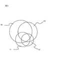
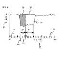
同一のウエハを検出方式の異なる検査装置A、Bで検査し、検出された異物や外観欠陥等の不良の座標を元に不良分布マップを作成すると、各々図2の101a、図3の101bのようになる。2つの不良分布マップの突き合わせ(重ね合わせ)チェックを行うと、検査装置A、Bの両方で検出した異物や外観欠陥等の不良102a、102b、その装置でのみ検出できた異物や外観欠陥等の不良103a、103b、その装置で検出できなかった異物や外観欠陥等の不良104a、104bを知ることができる。
【0008】
そこで、検出方式の異なる検査装置A、B、C、D各々の検出結果の不良分布マップの突き合わせチェック後のデータをもとに、ベン図を作成すると、図4ようになる。ここで、検査装置A、B、C、D各々の検出結果が10、11、12、13の円で、また、検出方式によらずに検出できる異物や外観欠陥等の不良が、円の重なり部分で表現される。
【0009】
検出方法が異なると、図4に示すように、特に検出感度ぎりぎりの微小な異物や外観欠陥等の不良の検出率に違いが生じる。その結果、せっかく検査装置を導入して検査を行っていても、場合によっては、致命的な不良の発生を見逃し、大量不良発生を許すこともある。従って、いかにして最適な検査装置を選ぶかということが、高い歩留まりを実現する上で重要な課題となっている。
【0010】
また、使用する検査装置が決まったとしても、検査頻度の設定は、製造ラインのエンジニアによりほとんど勘と経験に頼って決定されているため、検査工程の管理を自動化する上で、これを阻害する大きな要因となっていた。
【0011】
本発明の目的は、半導体ウエハ、プリント基板、TFT液晶表示装置、プラズマディスプレイ形表示装置、あるいは磁気ディスク基板等電子部品の製造において、検査すべき工程に対し、最適な検査装置と、これを用いた検査の頻度を設定する手段を供給することにより、高い歩留まりを確保できる製造方法と,この機能を有する製造管理システムを提供することにある。
【0012】
【課題を解決するための手段】
上記課題は、複数の検査装置の機種間の性能上の相関を求める手段、統計的に不良発生の間隔を求める手段、機種間の性能上の相関と不良発生頻度をもとに最適な検査装置とこれを用いた検査の頻度を設定する手段と、これに基づき検査装置群への物の流し方等を管理するシステムを有する製造方法を提供することにより解決することができる。
【0013】
具体的には、複数の処理工程から成る電子部品の製造ラインにおいて、所定の処理工程を経た該電子部品を性能の異なる複数の検査装置を用いてそれぞれが所定の頻度で抜き取り検査することで、その製造状況を管理する。
【0014】
より好ましくは、前記処理工程に投入された複数の電子部品に対して、前記複数の検査装置ではそれぞれが所定数毎に該電子部品を抜き取り検査しており、該検査結果に基づいて、該電子部品を所定数毎に検査する検査頻度をそれぞれの検査装置に設定する。
【0015】
この場合、前記検査結果から、前記複数の検査装置の検査頻度と該検査頻度で検査した場合の総合損失期待値との関数を導き、該総合損失期待値が最小となるように前記複数の検査装置の検査頻度をそれぞれに設定しても良い。
【0016】
従来のように、検査装置を固定して製造ラインを管理した場合、その検査装置の性能では検出できる欠陥はある程度限定されてしまう。一般に製造ラインの不良モードは時間とともに変化するので、その検査装置の検査結果からは正常である(管理基準を満たす)と判断していても、実際にはその検査装置では検出できなかった欠陥が原因で不良を作り込む場合が多い。
【0017】
検査装置としては、例えば外観検査装置や異物検査装置があるが、それぞれは欠陥の検出方式が異なるので、外観検査装置と異物検査装置とが共通に欠陥として検出する部分もあるが、一方でそれぞれにしか検出できない欠陥もある。また、それぞれに費やされる検査時間も問題であり、検査頻度が増せば当然、製造ライン全体でのスループットは低下してしまう。
【0018】
本発明は、このような実状を考慮したものであり、性能の異なる複数の検査装置を用いることで、不良モードの変化等に迅速に対応するものである。また、検査装置の検査頻度と該検査頻度で検査した場合の総合損失期待値との関数を導き、該総合損失期待値が最小となるように前記複数の検査装置の検査頻度をそれぞれに設定することで、電子部品を効率的に製造させている。
【0019】
つまり、例えば異物検査装置により10枚に1枚の頻度で検査しながら、外観検査装置により100枚に1枚の頻度で検査すれば、異物検査装置により検出できる欠陥と、外観検査装置により検出できる欠陥とが把握できるので、新規な不良モードに対しても迅速に対策することができし、その設定頻度もトータルな製造損失を考慮すれば、電子部品を効率的に製造できる。
図1は、本発明の概念を図示したものである。
【0020】
半導体ウエハ上の異物や外観欠陥等の不良の検査を例にとり説明する。なお、最近の異物検査装置は、画像処理技術の進歩により外観欠陥検査も可能となってきており、「散乱光検出形の外観検査装置」と位置付けることができるため、以下、両者をまとめて検査装置と呼ぶ。
【0021】
半導体製造ラインに、様々な検出方式を有する(従って、機種の異なる)検査装置A、B、C、D等からなる検査装置群1が存在するとする。各検査装置は、ネットワーク8に接続され、検査終了後に結果をデータ収集系2に転送する。データ収集系2は大規模なデータベース3を有し、同一ウエハの検査結果の工程履歴や、同一工程の不良発生推移等を解析する際に用いることができる。
【0022】
ある特定の不良モードが確認された場合、特定工程から選択した同一のウエハを検査装置群1の機種の異なる検査装置により検査したデータを収集し解析することにより、機種間の相関度を計算をすることができる(機種間相関度計算処理4)。一方、同一工程の不良発生経過を分析することにより、平均的な不良発生頻度を求めることができる(不良発生頻度計算処理5)。そして、機種間相関度計算処理4と不良発生頻度計算処理5の結果をもとに、最適な検査装置と検査頻度を逐次求め(最適機種・検査頻度計算処理6)、検査装置群管理システム7を介して、検査装置群1へのウエハの投入方法等を指示し制御すればよい。
【0023】
【発明の実施の形態】
本発明の実施の形態について、以下詳細に説明する。
【0024】
まず、図5から図12を用いて、機種間相関度計算処理4の実施の形態について、機種の異なる2つの検査装置をモデルに説明する。
【0025】
既に述べたように、同一のウエハを検出方式の異なる検査装置A、Bで検査し、検出された異物や外観欠陥等の不良の座標を元に不良分布マップを作成し、2つの不良分布マップの突き合わせ(重ね合わせ)チェックを行うと、検査装置A、Bの両方で検出した異物や外観欠陥等の不良、その装置でのみ検出できた異物や外観欠陥等の不良、その装置で検出できなかった異物や外観欠陥等の不良に分けて知ることができる。
【0026】
不良分布マップの作成にあたっては、検出されたすべての不良を対象にする場合と、レビュー(観察)結果に基づき特定の不良モードに対象を限定する場合とがある。
【0027】
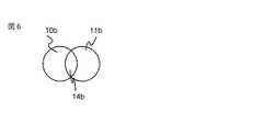
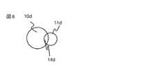
突き合わせ(重ね合わせ)チェックの結果をベン図に表示すると、図5から図8に示すような4つの場合に大きく分類できる。ここで、円として表示される10aから10d、11aから11dの大きさは、それぞれ検査装置A、Bにより検出された不良の数を表わす。そして、ふたつの円の重なり部分である12aから12dの面積は、検査装置A、Bの双方で共通に検出された不良の数を表わす。
【0028】
いま、検査装置A、Bにより検出された不良の数を、それぞれNa、Nb、双方で共通に検出された不良の数をNabと定義する。検査装置A、Bの少なくともいずれかで検出された不良の数Nallは数1により定義される。
【0029】
【数1】
そして、2機種間の相関度の有無は、数2、数3、数4等により計算される。
R1は、検査装置Aの検出不良数を基準とした検査装置Bの検出率を表わす(数2)。R2は、総不良数対する検査装置Aの捕捉率を表わす(数3)。R3は、検査装置Aの検出不良数を基準とした共通不良の検出率を表わす(数4)。そして、R1からR3に対して、各々T1からT3の閾値(例えば、各々0.9等)を設定する。
【0031】
【数2】
【数3】
【数4】
図5は、R1からR3の何れもが、各々T1からT3の閾値を越えた場合を示す。即ち、検査装置A、Bの両方が、ほぼ検出率の面からは同じ特性を有していることを表わし、検査装置の選定は、経済性を考慮して行われるべき場合である。
【0035】
図6は、R2あるいはR3が、各々T2あるいはT3の閾値以下の場合を示す。即ち、検査装置A、Bの双方が、検出方法等の違いでそれぞれ別個の不良を見つけている場合である。この場合、検出されている不良のモードが機種により異なる場合には、不良モードと致命度の関係を勘案して、両方の検査装置、もしくは重要性の高い不良モードを検出できる検査装置を用いる必要がある。検出されている不良のモードが同一の場合には、検査装置の選定は、R2の捕捉率と経済性を考慮して行われる。
【0036】
図7は、R1が閾値T1以下となり、従ってR3も閾値T3以下となる場合を示す。即ち、検査装置Aの性能が検査装置Bの性能を包含する場合であり、検査装置の選定は、R2の捕捉率と経済性を考慮して行われる。
【0037】
図8は、R1からR3の何れもが、各々T1からT3の閾値以下の場合を示す。検出されている不良のモードが機種により異なる場合には、検査装置Bで検出された不良モードと致命度の関係を勘案し、この不良モードの重要性が高い場合には検査装置Bを用いる検査も併用する必要がある。検出されている不良のモードが同一の場合には、検査装置の選定は、R2の捕捉率と経済性を考慮して行われる。
【0038】
図5から図8のベン図を用いた機種間相関度計算では、検出個数のみを考慮したが、検出レベルにまで踏み込んだ詳細な相関度計算を行う手法の例を、図9から図12に示す。
【0039】
図5または図7で示したようにベン図上での解析で2つの検査装置に相関がとれている場合に、横軸15に検査装置Aにおける不良検出レベル(散乱光強度や欠陥サイズ)を、縦軸16に検査装置Bにおける不良検出レベル(散乱光強度や欠陥サイズ)をとり、その共通検出不良をプロットすると18のような分布を得ることができる(図9、図10)。ここで、17が検査装置Aにおける検出限界となる。
【0040】
数5により求められる傾き係数mが検査装置Aを基準とした検査装置Bの検出レベル換算値となる。
【0041】
【数5】
そして、数6により求められる分散係数dが一定の閾値以下に収まるとき、検査装置A、Bは感度上の相関が大きいとして、取り扱うことができる。
【0043】
【数6】
図5または図7で示したようにベン図上での解析で2つの検査装置に相関がとれている場合に、横軸15に検査装置Aにおける不良検出レベル(散乱光強度や欠陥サイズ)を、縦軸19に検出した不良の個数をとり、検査装置Aでの検出結果20と、その内で検査装置Bとの共通検出不良21をプロットする(図11、図12)。ここで、不良検出レベルをもとに、23a〜23eの様にグループ化を行い、各々のグループにおいて、検査装置Aの平均検出不良数D1、その内で検査装置Bとの共通検出不良数E1を求め、数7により係数R4を計算する。
【0045】
【数7】
図11のように、全てのグループで係数R4が一定の閾値以上の値をとる場合、検査装置Aと検査装置Bとの差は、捕捉率の差であると言うことができる。しかし、特定のグループでR4が一定の閾値以下の値をとる場合、検査装置Bが不感帯を有することを表わす。例えば図12では、検査装置Bがレベル22以下の微小な不良を捕えることができないことを意味し、特に微小な不良での致命性が重要視される場合には、検査装置Bの選定は不可能となる。
【0047】
図1の発生頻度計算処理5については、設備の不良解析などで用いられるMTBF(Mean Time Between Failure)計算等の手法を用いることができる。
【0048】
次に、図1の機種間相関度計算処理4と不良発生頻度計算処理5の結果をもとに、最適な検査装置と検査頻度を求める最適機種・検査頻度計算処理6の実施の形態について以下に説明する。
【0049】
一般的に、高捕捉率の検査装置は高価でスループットも低く、高頻度検査に適さないこともあり、また、低捕捉率の検査装置は安価でスループットも高いが微小な不良を見逃すという傾向がある。そこで、最適な検査装置と検査頻度を求めるために、検査に要する費用Ciと不良作り込みによる損失期待値Cfの和で表わされる総合損失期待値Ct(数8)を指標にする方法を考案した。
【0050】
【数8】
図13、図14は検査による不良見逃しの概念を示したものである。
【0052】
図13は低い捕捉率の検査装置を用いる場合を示している。横軸30に製造ラインを流れるウエハの投入順序w1〜wnをとり縦棒32がウエハ1枚の投入を表わす。
縦軸31に良品率をとると、微小サイズの不良による歩留まり低下がwsの時点で発生すると、良品率の推移が折れ線34の様になる。33a〜33nは製造ラインを流れるウエハの内、検査のために抜き取られる物を表わす。図13の場合、低い捕捉率の検査装置を高頻度に用いた例を示しているが、不良が発生していても、捕捉率が低いために36の時点まで期間37の間は不良であることを認識できず不良ウエハを作り込んでしまう。良品率予想ライン35との間で挟まれた領域39が不良ウエハ作り込みのうち、検査装置起因の部分である。なお、ここで38は不良が検知されてから対策が完了するまでの期間を表わす。
【0053】
図14は低い検査頻度で検査装置を用いる場合を示している。図13同様、横軸30に製造ラインを流れるウエハの投入順序w1〜wnをとり縦棒32がウエハ1枚の投入を表わす。縦軸31に良品率をとると、不良による歩留まり低下がwsの時点で発生すると、良品率の推移が折れ線34の様になる。低い検査頻度で検査装置を用いるために、検出しやすい大きな不良が発生していても、検査装置にかけられる36の時点まで期間37の間は不良であることを認識できず不良ウエハを作り込んでしまう。良品率予想ライン35との間で挟まれた領域39が不良ウエハ作り込みのうち、検査装置起因の部分である。
【0054】
検査に要する費用Ciは、まず、検査1回あたりに要する費用Csを求めることから始める。検査1回あたりに要する費用Csは、検査装置価格、検査装置維持費、検査装置稼働時間、全面検査時(検査エリア率100%)のスループット、検査エリア率等のデータをもとに計算される(数9)。
【0055】
【数9】
ここで、f1、f2は関数である。
【0057】
次に、統計的に求められた不良発生頻度(間隔)Mfと検査頻度Fr(検査抜き取り間隔)をもとに、不良ウエハを検査するまでの検査回数N1を求め(数10)、さらに、不良ウエハを抜き取ってからこれを不良と認識するまでの平均検査回数N2を求め(数11)、これらをまとめて最終的な検査費用を求める(数12)。
【0058】
【数10】
【数11】
【数12】
ここで、f3は関数である。
【0062】
なお、検出確率(不良ウエハを検査して不良と認識するための確率)は、検査エリア率(総チップ数に対する検査チップの割合)、管理基準(例えば不良チップ率)、捕捉率等から求められる(数13)。
【0063】
【数13】
ここで、f4は関数である。
【0065】
一方、不良作り込み損失期待値Cfは、ウエハ価格、検査頻度Fr(検査抜き取り間隔)、不良ウエハを抜き取ってからこれを不良と認識するまでの平均検査回数N2、不良が検知されてから対策が完了するまでの期間等をもとに計算される(数14)。
【0066】
【数14】
ここで、f5は関数である。
【0068】
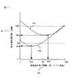
図15は、検査頻度Fr(検査抜き取り間隔)を横軸40に、検査費用Ci、不良作り込み損失期待値Cf、総合損失期待値Ctを縦軸41にとり、両対数グラフを作成したものである。検査費用Ciは、42の様に検査頻度が少なくなる(検査抜き取り間隔が長くなる)につれて減少する。一方、不良作り込み損失期待値Cfは、43の様に検査頻度が少なくなる(検査抜き取り間隔が長くなる)につれて増加する。従って、これらを足し合わせた総合損失期待値Ctは、44のようになる。そして、総合損失期待値Ctが最小値46をとる際の検査頻度Fr(検査抜き取り間隔)が最適検査頻度45となる。
【0069】
図16は、検査頻度Fr(検査抜き取り間隔)を横軸40に、総合損失期待値Ctを縦軸41にとり、捕捉率を変化させてプロットしたものである。44aから44cまで検査装置の捕捉率が低下するに従い、総合損失期待値の最小値は46aから46cまで増加し、一方、最適検査頻度も45aから45cまで高頻度化が要求されることがわかる。
【0070】
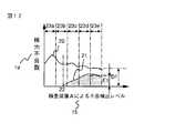
図17は、検査頻度Fr(検査抜き取り間隔)を横軸40に、総合損失期待値Ctを縦軸41にとり、機種の異なる2つの検査装置について、捕捉率等も勘案してプロットした例である。この場合、低価格でスループットの高い装置を用いて(44d)検査頻度を45dに設定した場合44dの方が、高価格でスループットの低い装置を用いる場合(44e)よりも、総合損失期待値Ctを下げることができる。
【0071】
従って、変動する不良モードの捕捉率を、図1の機種間相関度計算処理4より求め、一方、不良の不良発生頻度を図1の不良発生頻度計算処理5より求め、総合損失期待値Ctを計算することにより、実時間で最適な検査装置と検査頻度を設定することが可能となる。
【0072】
図18は、不良モードが未知である場合の対応の仕方の例を示したものである。図13、図14に示したように、低捕捉率・高頻度の検査だけ、あるいは高捕捉率・低頻度の検査だけでは、未知の見逃しに対して無力な場合がある。そこで、両者の欠点を補う検査手法が重要である。
【0073】
低捕捉率・高頻度の検査装置44dでは、本来検査頻度を45dに設定したときに総合損失期待値46dを得る。しかし、微小不良に対する見逃しは存在する。微小不良を検出するためには、高捕捉率の検査装置が必要であるが、場合によっては、44eに示すように、本来検査頻度を45eに設定したときに総合損失期待値46eが、低捕捉率・高頻度の検査装置を用いた場合の総合損失期待値46dを上回ってしまう。そこで、高捕捉率の検査装置の検査頻度を45e'と下げて使用し、これを低捕捉率・高頻度の検査装置と併用することにより(44f)、低捕捉率の検査装置の最適な検査頻度45fと、この時の総合損失期待値46fを得ることができる。
【0074】
このようにして、最適な検査装置と検査頻度を逐次求め(最適機種・検査頻度計算処理6)、検査装置群管理システム7を介して、検査装置群1へのウエハの投入方法等を指示し制御する。
【0075】
図19は、本発明による検査の流れに関する概念をまとめたものである。先ず、検査頻度等検査装置へのウエハの流し方を過去の経験等に基づき初期設定する(50)。ウエハを投入し(51)、低捕捉率(低感度)検査装置による高頻度検査を実施する(52)。管理基準との比較を行い(53a)、基準を越えていた場合、アラームを発信し(58a)、新しい不良モードの場合(60)、高捕捉率(高感度)検査装置による詳細検査を行った後(59b)、突き合わせ解析等により、機種間の捕捉率等を計算し(61)、さらに、検査頻度等の再設定(56b)を行い次のウエハに移る(57)。
【0076】
旧来の不良モードの場合には、検査頻度等の再設定(56b)を行い次のウエハに移る(57)。
【0077】
管理基準との比較を行い(53a)、基準を越えなかった場合、一定間隔でウエハを抜き取り(54)、高捕捉率(高感度)検査装置による検査を行う(59a)。
【0078】
管理基準との比較を行い(53b)、基準を越えていた場合、アラームを発信した後(58b)、突き合わせ解析等により、機種間の捕捉率等を計算し(61)、さらに、検査頻度等の再設定(56b)を行い次のウエハに移る(57)。
【0079】
管理基準との比較を行い(53b)、基準を越えなかった場合、不良発生頻度の低下の有無をチェックし(55)、頻度低下が見られるとき、検査頻度等の再設定(56b)を行い次のウエハに移る(57)。
【0080】
本発明の実施例は、半導体ウエハ上の異物や外観欠陥の検査を例にとり、説明を行ったが、検査の対象としては、線幅、膜厚、色等の物理データであっても同様に考えられ、例えば、実施例の低捕捉率検査装置を相対変化測定用モニタに、高捕捉率検査装置を高感度絶対値測定装置に置き換えれば、同様の手法が成り立つ。
【0081】
また、製品の対象も半導体ウエハに留まらず、プリント基板、TFT液晶表示装置、プラズマディスプレイ形表示装置、あるいは磁気ディスク基板等、広範囲の電子部品の製造に適用できる。
【0082】
【発明の効果】
以上、本発明によれば、半導体ウエハ、プリント基板、TFT液晶表示装置、プラズマディスプレイ形表示装置、あるいは磁気ディスク基板等電子部品の製造において、適用検査装置、検査頻度等、複雑な検査条件を容易に設定することができると共に、総合損失期待値最小という操作を行うことにより、検査の経済効率の向上に大きく寄与することができる。
【図面の簡単な説明】
【図1】本発明の実施例を示す処理機能ブロック図。
【図2】異なる検査装置A、Bで検査した際の不良分布マップ。
【図3】異なる検査装置A、Bで検査した際の不良分布マップ。
【図4】検出方式の異なる検査装置による検出不良のベン図表示。
【図5】実施例に基づき、検出不良数により機種間の相関度を求めるベン図表示。
【図6】実施例に基づき、検出不良数により機種間の相関度を求めるベン図表示。
【図7】実施例に基づき、検出不良数により機種間の相関度を求めるベン図表示。
【図8】実施例に基づき、検出不良数により機種間の相関度を求めるベン図表示。
【図9】実施例に基づき、検出レベルにより機種間の相関度を求めるためのグラフ。
【図10】実施例に基づき、検出レベルにより機種間の相関度を求めるためのグラフ。
【図11】実施例に基づき、検出レベル別の検出不良数により機種間の相関度を求めるためのグラフ。
【図12】実施例に基づき、検出レベル別の検出不良数により機種間の相関度を求めるためのグラフ。
【図13】検査による不良見逃しの概念を示す図。
【図14】検査による不良見逃しの概念を示す図。
【図15】総合損失期待値計算の概念を示す図。
【図16】状況により、検査条件を最適化する方法を説明する図。
【図17】状況により、検査条件を最適化する方法を説明する図。
【図18】状況により、検査条件を最適化する方法を説明する図。
【図19】本発明による検査の流れに関する概念を示す図である。
【符号の説明】
1…検査装置群、2…データ収集系、4…機種間相関度計算、5…不良発生頻度計算、6…最適機種・検査頻度計算、7…検査装置群管理システム、10…検査装置Aによる検出不良数、11…検査装置Bによる検出不良数、42…検査費用、43…不良作り込み損失期待値、44…総合損失期待値、45…最適検査頻度、46…総合損失期待値最小値。[0001]
BACKGROUND OF THE INVENTION
The present invention relates to a method and a manufacturing management system for manufacturing an electronic component such as a semiconductor wafer, a printed circuit board, a TFT liquid crystal display device, a plasma display type display device, or a magnetic disk substrate with a high yield.
[0002]
[Prior art]
In the manufacture of electronic components such as semiconductor wafers, printed circuit boards, TFT liquid crystal display devices, plasma display type display devices, and magnetic disk substrates, which are becoming finer and more complex year by year, how to secure a high yield has become a major issue. ing.
[0003]
Factors that hinder the yield include (1) foreign matter and appearance defects (including abnormal crystal growth and disconnection, short-circuiting, missing, etc.), (2) misalignment, defocus, film thickness abnormality, etching abnormality, etc. There is a pattern formation defect (pattern width defect or the like). In mass production of electronic components, these defects are discrete (for example, one out of several in a semiconductor wafer manufacturing, a single defect occurs) or continuous (for example, every several in a semiconductor wafer manufacturing). Occur once in a row).
[0004]
Conventionally, in order to avoid these discrete defects or continuous defects, a method has been adopted in which inspection is performed in main processes during manufacturing, defects are detected, and countermeasures are taken.
[0005]
Taking foreign matter inspection as an example, there are many detection methods for minute foreign matter existing on electronic parts on which a pattern such as a semiconductor wafer is formed in Japanese Patent Laid-Open Nos. 55-149829 and 59-65428. It is disclosed. Various inspection apparatuses employing these detection methods have been developed and used in production lines.
[0006]
[Problems to be solved by the invention]
Therefore, the problem to be solved by the present invention will be described by taking the inspection of foreign matters and appearance defects on the wafer as an example.
[0007]
When the same wafer is inspected by inspection apparatuses A and B having different detection methods, and defect distribution maps are created based on the detected coordinates of defects such as foreign matter and appearance defects, 101a in FIG. 2 and 101b in FIG. It becomes like this. When the matching (overlay) check of two defect distribution maps is performed,
[0008]
Therefore, when a Venn diagram is created based on the data after the matching check of the defect distribution maps of the detection results of the inspection apparatuses A, B, C, and D having different detection methods, FIG. 4 is obtained. Here, the detection results of inspection apparatuses A, B, C, and D are circles of 10, 11, 12, and 13, and defects such as foreign matters and appearance defects that can be detected regardless of the detection method are overlapped by circles. Expressed in parts.
[0009]
If the detection method is different, as shown in FIG. 4, there is a difference in the detection rate of defects such as a minute foreign substance with a detection sensitivity that is very small and an appearance defect. As a result, even if an inspection apparatus is introduced for inspection, in some cases, the occurrence of a fatal defect may be missed, and a large number of defects may be allowed. Therefore, how to select an optimal inspection apparatus is an important issue in realizing a high yield.
[0010]
Even if the inspection equipment to be used is decided, the setting of the inspection frequency is determined by the engineers on the production line almost relying on intuition and experience, which hinders this in automating the inspection process management. It was a big factor.
[0011]
An object of the present invention is to use an inspection apparatus that is optimal for the process to be inspected in the manufacture of electronic components such as a semiconductor wafer, a printed circuit board, a TFT liquid crystal display device, a plasma display type display device, or a magnetic disk substrate. Another object of the present invention is to provide a manufacturing method capable of ensuring a high yield by supplying means for setting the frequency of inspection, and a manufacturing management system having this function.
[0012]
[Means for Solving the Problems]
The above-mentioned problems include means for obtaining a correlation in performance between models of a plurality of inspection apparatuses, means for obtaining a statistical interval for occurrence of defects, and an optimum inspection apparatus based on the correlation in performance between models and the frequency of occurrence of defects. It is possible to solve the problem by providing a manufacturing method having a system for setting the frequency of inspection using this and a means for managing the flow of objects to the group of inspection devices based on this.
[0013]
Specifically, in a production line of electronic parts composed of a plurality of processing steps, each of the electronic components that have undergone a predetermined processing step is sampled and inspected at a predetermined frequency using a plurality of inspection devices having different performances. Manage its manufacturing status.
[0014]
More preferably, with respect to the plurality of electronic components put into the processing step, each of the plurality of inspection devices samples and inspects the electronic components every predetermined number, and based on the inspection result, the electronic components The inspection frequency for inspecting the parts every predetermined number is set in each inspection apparatus.
[0015]
In this case, a function of the inspection frequency of the plurality of inspection devices and the total loss expected value when inspected at the inspection frequency is derived from the inspection result, and the plurality of inspections are performed so that the total loss expected value is minimized. The inspection frequency of the apparatus may be set for each.
[0016]
When the inspection apparatus is fixed and the production line is managed as in the prior art, defects that can be detected are limited to some extent by the performance of the inspection apparatus. In general, the failure mode of a production line changes with time, so even if it is judged that the inspection device is normal (satisfying the management criteria) from the inspection results of the inspection device, there are actually defects that could not be detected by the inspection device. In many cases, the cause is a defect.
[0017]
As the inspection device, for example, there are an appearance inspection device and a foreign matter inspection device, but since each has a different detection method of defects, there are parts that the appearance inspection device and the foreign matter inspection device detect as defects in common, but on the other hand Some defects can only be detected. In addition, the inspection time spent for each is a problem, and as the inspection frequency increases, the throughput of the entire production line naturally decreases.
[0018]
The present invention takes such actual situations into consideration, and uses a plurality of inspection apparatuses having different performances to quickly respond to a change in a defective mode. In addition, a function of the inspection frequency of the inspection apparatus and the expected total loss value when inspected at the inspection frequency is derived, and the inspection frequencies of the plurality of inspection apparatuses are respectively set so that the total loss expected value is minimized. Thus, electronic parts are efficiently manufactured.
[0019]
In other words, for example, if inspection is performed with a frequency of 1 in 10 with a foreign substance inspection apparatus and inspection is performed with a frequency of 1 in 100 with a visual inspection apparatus, defects that can be detected with the foreign object inspection apparatus can be detected with the visual inspection apparatus. Since the defect can be grasped, it is possible to take a quick countermeasure against a new failure mode, and the electronic component can be efficiently manufactured if the set frequency takes into account the total manufacturing loss.
FIG. 1 illustrates the concept of the present invention.
[0020]
An example of inspection for defects such as foreign matter and appearance defects on a semiconductor wafer will be described. In addition, recent foreign matter inspection devices are also capable of visual defect inspection due to advances in image processing technology, and can be positioned as a “scattered light detection type visual inspection device”. Called a device.
[0021]
It is assumed that an
[0022]
When a specific failure mode is confirmed, the correlation between the models is calculated by collecting and analyzing data obtained by inspecting the same wafer selected from the specific process by an inspection apparatus of a different type in the
[0023]
DETAILED DESCRIPTION OF THE INVENTION
Embodiments of the present invention will be described in detail below.
[0024]
First, with reference to FIGS. 5 to 12, an embodiment of the inter-model
[0025]
As described above, the same wafer is inspected by inspection apparatuses A and B with different detection methods, and a defect distribution map is created based on the detected coordinates of defects such as foreign matter and appearance defects, and two defect distribution maps are created. If a butt (overlay) check is performed, defects such as foreign matter and appearance defects detected by both inspection apparatuses A and B, defects such as foreign matter and appearance defects that can be detected only by that apparatus, cannot be detected by that apparatus It is possible to know by dividing it into defects such as foreign matter and appearance defects.
[0026]
In creating the defect distribution map, there are a case where all detected defects are targeted and a case where a target is limited to a specific defect mode based on a review (observation) result.
[0027]
When the result of the matching (superposition) check is displayed on the Venn diagram, it can be roughly classified into four cases as shown in FIGS. Here, the sizes of 10a to 10d and 11a to 11d displayed as circles represent the number of defects detected by the inspection apparatuses A and B, respectively. The area of 12a to 12d, which is the overlapping portion of the two circles, represents the number of defects detected in common in both inspection apparatuses A and B.
[0028]
Now, the number of defects detected by the inspection apparatuses A and B is defined as Na and Nb, respectively, and the number of defects detected in both is defined as Nab. The number Nall of defects detected by at least one of the inspection apparatuses A and B is defined by
[0029]
[Expression 1]
The presence / absence of the correlation between the two models is calculated by
R1 represents the detection rate of the inspection apparatus B based on the number of detection failures of the inspection apparatus A (Equation 2). R2 represents the capture rate of the inspection apparatus A with respect to the total number of defects (Equation 3). R3 represents a common defect detection rate based on the number of detected defects of the inspection apparatus A (Equation 4). Then, threshold values of T1 to T3 (for example, 0.9, etc.) are set for R1 to R3, respectively.
[0031]
[Expression 2]
[Equation 3]
[Expression 4]
FIG. 5 shows a case where any of R1 to R3 exceeds the thresholds T1 to T3, respectively. That is, both inspection apparatuses A and B have the same characteristics in terms of detection rate, and the selection of the inspection apparatus should be performed in consideration of economy.
[0035]
FIG. 6 shows a case where R2 or R3 is equal to or less than the threshold value of T2 or T3, respectively. That is, both inspection apparatuses A and B have found separate defects due to differences in detection methods and the like. In this case, if the detected failure mode differs depending on the model, it is necessary to consider both the failure mode and the criticality, and use both inspection devices or an inspection device that can detect failure modes with high importance. There is. When the detected failure mode is the same, the inspection apparatus is selected in consideration of the capture rate and economic efficiency of R2.
[0036]
FIG. 7 shows a case where R1 is equal to or less than the threshold value T1, and thus R3 is also equal to or less than the threshold value T3. That is, the performance of the inspection apparatus A includes the performance of the inspection apparatus B, and the inspection apparatus is selected in consideration of the capture rate of R2 and the economy.
[0037]
FIG. 8 shows a case where each of R1 to R3 is less than or equal to the threshold value of T1 to T3. When the detected failure mode differs depending on the model, the relationship between the failure mode detected by the inspection apparatus B and the criticality is taken into consideration, and when the failure mode is highly important, the inspection using the inspection apparatus B is performed. Need to be used together. When the detected failure mode is the same, the inspection apparatus is selected in consideration of the capture rate and economic efficiency of R2.
[0038]
In the correlation calculation between models using the Venn diagrams of FIGS. 5 to 8, only the number of detections is considered, but an example of a method for performing detailed correlation calculation down to the detection level is shown in FIGS. 9 to 12. .
[0039]
As shown in FIG. 5 or FIG. 7, when two inspection apparatuses are correlated in the analysis on the Venn diagram, the
[0040]
The slope coefficient m obtained by Equation 5 is a detection level converted value of the inspection apparatus B with the inspection apparatus A as a reference.
[0041]
[Equation 5]
And when the dispersion coefficient d calculated | required by
[0043]
[Formula 6]
As shown in FIG. 5 or FIG. 7, when two inspection apparatuses are correlated in the analysis on the Venn diagram, the
[0045]
[Expression 7]
As shown in FIG. 11, when the coefficient R4 has a value equal to or larger than a certain threshold value in all groups, it can be said that the difference between the inspection apparatus A and the inspection apparatus B is a difference in capture rate. However, when R4 takes a value equal to or smaller than a certain threshold value in a specific group, it indicates that the inspection apparatus B has a dead zone. For example, in FIG. 12, this means that the inspection apparatus B cannot catch a minute defect of
[0047]
For the occurrence frequency calculation process 5 in FIG. 1, a technique such as MTBF (Mean Time Between Failure) calculation used in equipment failure analysis or the like can be used.
[0048]
Next, based on the results of the inter-model
[0049]
In general, inspection devices with high capture rates are expensive and have low throughput, and may not be suitable for high-frequency inspections. Inspection devices with low capture rates are inexpensive and have high throughput, but tend to miss minute defects. is there. Therefore, in order to find the optimal inspection device and inspection frequency, a method was devised that uses the total loss expected value Ct (Equation 8), which is expressed as the sum of the cost Ci required for inspection and the expected loss value Cf due to defect creation, as an index. .
[0050]
[Equation 8]
FIG. 13 and FIG. 14 show the concept of missing a defect by inspection.
[0052]
FIG. 13 shows a case where an inspection apparatus with a low capture rate is used. The
When the yield rate is taken along the
[0053]
FIG. 14 shows a case where the inspection apparatus is used at a low inspection frequency. As in FIG. 13, the
[0054]
The cost Ci required for the inspection starts by obtaining the cost Cs required for one inspection. Cost Cs required for each inspection is calculated based on data such as inspection device price, inspection device maintenance cost, inspection device operating time, throughput during full inspection (
[0055]
[Equation 9]
Here, f1 and f2 are functions.
[0057]
Next, based on the statistically determined defect occurrence frequency (interval) Mf and inspection frequency Fr (inspection sampling interval), the number of inspections N1 until the defective wafer is inspected is calculated (Equation 10), The average number of inspections N2 from when the wafer is extracted until it is recognized as defective is obtained (Equation 11), and these are collected together to obtain the final inspection cost (Equation 12).
[0058]
[Expression 10]
[Expression 11]
[Expression 12]
Here, f3 is a function.
[0062]
The detection probability (probability for inspecting a defective wafer to recognize it as defective) is obtained from the inspection area ratio (ratio of inspection chips to the total number of chips), management criteria (for example, defective chip ratio), capture rate, and the like. (Equation 13).
[0063]
[Formula 13]
Here, f4 is a function.
[0065]
On the other hand, the expected defect-making loss Cf is the wafer price, inspection frequency Fr (inspection sampling interval), the average number of inspections N2 from when a defective wafer is extracted until it is recognized as defective, and measures are taken after a defect is detected. It is calculated based on the period until completion (Equation 14).
[0066]
[Expression 14]
Here, f5 is a function.
[0068]
FIG. 15 is a log-log graph in which the inspection frequency Fr (inspection sampling interval) is plotted on the
[0069]
FIG. 16 is plotted with the capture rate varied with the inspection frequency Fr (inspection sampling interval) on the
[0070]
FIG. 17 is an example in which the inspection frequency Fr (inspection sampling interval) is plotted on the
[0071]
Accordingly, the capture rate of the fluctuating failure mode is obtained from the inter-model
[0072]
FIG. 18 shows an example of how to cope when the failure mode is unknown. As shown in FIG. 13 and FIG. 14, only low-acquisition rate / high-frequency inspection or only high-acquisition rate / low-frequency inspection may be ineffective against unknown oversight. Therefore, an inspection method that compensates for the disadvantages of both is important.
[0073]
The low capture rate / high
[0074]
In this way, the optimum inspection apparatus and inspection frequency are sequentially obtained (optimum model / inspection frequency calculation process 6), and a method for injecting wafers into the
[0075]
FIG. 19 summarizes the concepts related to the flow of inspection according to the present invention. First, the wafer flow to the inspection apparatus such as the inspection frequency is initially set based on past experience (50). A wafer is loaded (51), and high-frequency inspection is performed by a low capture rate (low sensitivity) inspection device (52). Compared with the control standard (53a), if the standard is exceeded, an alarm is issued (58a), and in the case of a new failure mode (60), a detailed inspection is performed with a high capture rate (high sensitivity) inspection device After (59b), the capture rate between the models is calculated by a matching analysis or the like (61), and the inspection frequency is reset (56b) to move to the next wafer (57).
[0076]
In the case of the conventional failure mode, the inspection frequency and the like are reset (56b) and the next wafer is moved (57).
[0077]
Comparison with the control standard is performed (53a). If the standard is not exceeded, the wafer is extracted at regular intervals (54) and inspected by a high capture rate (high sensitivity) inspection device (59a).
[0078]
Compared with the management standard (53b), if it exceeds the standard, after issuing an alarm (58b), calculate the capture rate between the models by matching analysis etc. (61), and also the inspection frequency, etc. Is reset (56b) to move to the next wafer (57).
[0079]
Compare with the management standard (53b), and if it does not exceed the standard, check if there is a decrease in the frequency of defects (55), and if the frequency decreases, reset the inspection frequency etc. (56b) Move to next wafer (57).
[0080]
The embodiments of the present invention have been described by taking the inspection of foreign matters and appearance defects on a semiconductor wafer as an example. However, the inspection target is the same even for physical data such as line width, film thickness, and color. For example, if the low capture rate inspection device of the embodiment is replaced with a relative change measurement monitor and the high capture rate inspection device is replaced with a high sensitivity absolute value measurement device, the same method can be established.
[0081]
Further, the object of the product is not limited to a semiconductor wafer, and can be applied to manufacture a wide range of electronic components such as a printed circuit board, a TFT liquid crystal display device, a plasma display type display device, or a magnetic disk substrate.
[0082]
【The invention's effect】
As described above, according to the present invention, in the manufacture of electronic components such as a semiconductor wafer, a printed circuit board, a TFT liquid crystal display device, a plasma display type display device, or a magnetic disk substrate, complicated inspection conditions such as an applicable inspection device and inspection frequency can be easily obtained. By setting the total loss expectation value to the minimum, it is possible to greatly contribute to the improvement of the economic efficiency of the inspection.
[Brief description of the drawings]
FIG. 1 is a processing function block diagram showing an embodiment of the present invention.
FIG. 2 is a defect distribution map when inspected by different inspection apparatuses A and B.
FIG. 3 is a defect distribution map when inspected by different inspection apparatuses A and B.
FIG. 4 is a Venn diagram display of detection failures by inspection apparatuses with different detection methods.
FIG. 5 is a Venn diagram display for obtaining the degree of correlation between models based on the number of detected defects based on the embodiment.
FIG. 6 is a Venn diagram display for determining the degree of correlation between models based on the number of detected defects based on the embodiment.
FIG. 7 is a Venn diagram display for obtaining the degree of correlation between models based on the number of detected defects based on the embodiment.
FIG. 8 is a Venn diagram display for obtaining the degree of correlation between models based on the number of detected defects based on the embodiment.
FIG. 9 is a graph for obtaining a correlation degree between models based on a detection level based on an embodiment.
FIG. 10 is a graph for obtaining a correlation degree between models based on a detection level based on an embodiment.
FIG. 11 is a graph for obtaining the degree of correlation between models based on the number of detection failures by detection level based on the embodiment.
FIG. 12 is a graph for obtaining the degree of correlation between models based on the number of detection failures by detection level based on the embodiment.
FIG. 13 is a diagram showing a concept of missing a defect by inspection.
FIG. 14 is a diagram showing a concept of missing a defect by inspection.
FIG. 15 is a diagram showing a concept of total loss expected value calculation.
FIG. 16 is a diagram for explaining a method for optimizing an inspection condition depending on a situation.
FIG. 17 is a diagram for explaining a method for optimizing an inspection condition depending on a situation.
FIG. 18 is a diagram for explaining a method for optimizing an inspection condition depending on a situation.
FIG. 19 is a diagram showing a concept relating to a flow of inspection according to the present invention.
[Explanation of symbols]
DESCRIPTION OF
Claims (5)
Translated fromJapanesePriority Applications (2)
| Application Number | Priority Date | Filing Date | Title |
|---|---|---|---|
| JP8020096AJP3699776B2 (en) | 1996-04-02 | 1996-04-02 | Manufacturing method of electronic parts |
| US08/831,298US6002989A (en) | 1996-04-02 | 1997-04-01 | System for quality control where inspection frequency of inspection apparatus is reset to minimize expected total loss based on derived frequency function and loss value |
Applications Claiming Priority (1)
| Application Number | Priority Date | Filing Date | Title |
|---|---|---|---|
| JP8020096AJP3699776B2 (en) | 1996-04-02 | 1996-04-02 | Manufacturing method of electronic parts |
Publications (2)
| Publication Number | Publication Date |
|---|---|
| JPH09269294A JPH09269294A (en) | 1997-10-14 |
| JP3699776B2true JP3699776B2 (en) | 2005-09-28 |
Family
ID=13711753
Family Applications (1)
| Application Number | Title | Priority Date | Filing Date |
|---|---|---|---|
| JP8020096AExpired - Fee RelatedJP3699776B2 (en) | 1996-04-02 | 1996-04-02 | Manufacturing method of electronic parts |
Country Status (2)
| Country | Link |
|---|---|
| US (1) | US6002989A (en) |
| JP (1) | JP3699776B2 (en) |
Cited By (2)
| Publication number | Priority date | Publication date | Assignee | Title |
|---|---|---|---|---|
| CN102650875A (en)* | 2011-02-25 | 2012-08-29 | 欧姆龙株式会社 | Inspection system, management server, inspection apparatus and method for managing inspection data |
| CN105628705A (en)* | 2015-12-22 | 2016-06-01 | 河南中烟工业有限责任公司 | Automatic deviation detection, alarm and rectification method for moisture meters in loosening and conditioning process |
Families Citing this family (49)
| Publication number | Priority date | Publication date | Assignee | Title |
|---|---|---|---|---|
| JP3055516B2 (en)* | 1997-12-25 | 2000-06-26 | 日本電気株式会社 | Apparatus and method for inspecting and analyzing semiconductor integrated circuit, and recording medium recording control program therefor |
| US6324481B1 (en)* | 1998-10-21 | 2001-11-27 | Texas Instruments Incorporated | Method for the calculation of wafer probe yield limits from in-line defect monitor data |
| US7069101B1 (en) | 1999-07-29 | 2006-06-27 | Applied Materials, Inc. | Computer integrated manufacturing techniques |
| JP2001118899A (en)* | 1999-10-19 | 2001-04-27 | Mitsubishi Electric Corp | Foreign matter and pattern defect inspection equipment |
| WO2001050209A1 (en)* | 1999-12-30 | 2001-07-12 | General Electric Company | Method and system for monitoring production data |
| US6469518B1 (en)* | 2000-01-07 | 2002-10-22 | Advanced Micro Devices, Inc. | Method and apparatus for determining measurement frequency based on hardware age and usage |
| US6871112B1 (en)* | 2000-01-07 | 2005-03-22 | Advanced Micro Devices, Inc. | Method for requesting trace data reports from FDC semiconductor fabrication processes |
| JP3784603B2 (en)* | 2000-03-02 | 2006-06-14 | 株式会社日立製作所 | Inspection method and apparatus, and inspection condition setting method in inspection apparatus |
| AU2001251144A1 (en)* | 2000-03-31 | 2001-10-15 | Advanced Bionics Corporation | High contact count, sub-miniature, fully implantable cochlear prosthesis |
| US6708074B1 (en) | 2000-08-11 | 2004-03-16 | Applied Materials, Inc. | Generic interface builder |
| US7188142B2 (en) | 2000-11-30 | 2007-03-06 | Applied Materials, Inc. | Dynamic subject information generation in message services of distributed object systems in a semiconductor assembly line facility |
| JP4649051B2 (en)* | 2001-03-21 | 2011-03-09 | オリンパス株式会社 | Inspection screen display method and substrate inspection system |
| US6970757B1 (en)* | 2001-04-19 | 2005-11-29 | Advanced Micro Devices, Inc. | Method and apparatus for updating control state variables of a process control model based on rework data |
| US6910947B2 (en) | 2001-06-19 | 2005-06-28 | Applied Materials, Inc. | Control of chemical mechanical polishing pad conditioner directional velocity to improve pad life |
| US7082345B2 (en) | 2001-06-19 | 2006-07-25 | Applied Materials, Inc. | Method, system and medium for process control for the matching of tools, chambers and/or other semiconductor-related entities |
| US7698012B2 (en) | 2001-06-19 | 2010-04-13 | Applied Materials, Inc. | Dynamic metrology schemes and sampling schemes for advanced process control in semiconductor processing |
| US7160739B2 (en) | 2001-06-19 | 2007-01-09 | Applied Materials, Inc. | Feedback control of a chemical mechanical polishing device providing manipulation of removal rate profiles |
| US7201936B2 (en) | 2001-06-19 | 2007-04-10 | Applied Materials, Inc. | Method of feedback control of sub-atmospheric chemical vapor deposition processes |
| US6913938B2 (en) | 2001-06-19 | 2005-07-05 | Applied Materials, Inc. | Feedback control of plasma-enhanced chemical vapor deposition processes |
| US7101799B2 (en) | 2001-06-19 | 2006-09-05 | Applied Materials, Inc. | Feedforward and feedback control for conditioning of chemical mechanical polishing pad |
| JP2003004657A (en) | 2001-06-25 | 2003-01-08 | Hitachi Ltd | Observation work support system |
| US7337019B2 (en) | 2001-07-16 | 2008-02-26 | Applied Materials, Inc. | Integration of fault detection with run-to-run control |
| US6984198B2 (en) | 2001-08-14 | 2006-01-10 | Applied Materials, Inc. | Experiment management system, method and medium |
| US6821792B1 (en)* | 2001-12-18 | 2004-11-23 | Advanced Micro Devices, Inc. | Method and apparatus for determining a sampling plan based on process and equipment state information |
| US6650955B1 (en)* | 2001-12-18 | 2003-11-18 | Advanced Micro Devices, Inc. | Method and apparatus for determining a sampling plan based on process and equipment fingerprinting |
| US7225047B2 (en) | 2002-03-19 | 2007-05-29 | Applied Materials, Inc. | Method, system and medium for controlling semiconductor wafer processes using critical dimension measurements |
| US20030199112A1 (en) | 2002-03-22 | 2003-10-23 | Applied Materials, Inc. | Copper wiring module control |
| US6687561B1 (en)* | 2002-04-03 | 2004-02-03 | Advanced Micro Devices, Inc. | Method and apparatus for determining a sampling plan based on defectivity |
| JP2005535130A (en) | 2002-08-01 | 2005-11-17 | アプライド マテリアルズ インコーポレイテッド | Methods, systems, and media for handling misrepresented measurement data in modern process control systems |
| US7272459B2 (en) | 2002-11-15 | 2007-09-18 | Applied Materials, Inc. | Method, system and medium for controlling manufacture process having multivariate input parameters |
| US8017411B2 (en)* | 2002-12-18 | 2011-09-13 | GlobalFoundries, Inc. | Dynamic adaptive sampling rate for model prediction |
| US7333871B2 (en) | 2003-01-21 | 2008-02-19 | Applied Materials, Inc. | Automated design and execution of experiments with integrated model creation for semiconductor manufacturing tools |
| US6766214B1 (en)* | 2003-04-03 | 2004-07-20 | Advanced Micro Devices, Inc. | Adjusting a sampling rate based on state estimation results |
| US7205228B2 (en) | 2003-06-03 | 2007-04-17 | Applied Materials, Inc. | Selective metal encapsulation schemes |
| WO2005008737A2 (en)* | 2003-07-14 | 2005-01-27 | August Technology Corporation | Inspection and metrology module cluster tool with multi-tool manager |
| US7354332B2 (en) | 2003-08-04 | 2008-04-08 | Applied Materials, Inc. | Technique for process-qualifying a semiconductor manufacturing tool using metrology data |
| US7356377B2 (en) | 2004-01-29 | 2008-04-08 | Applied Materials, Inc. | System, method, and medium for monitoring performance of an advanced process control system |
| US6961626B1 (en) | 2004-05-28 | 2005-11-01 | Applied Materials, Inc | Dynamic offset and feedback threshold |
| US7096085B2 (en) | 2004-05-28 | 2006-08-22 | Applied Materials | Process control by distinguishing a white noise component of a process variance |
| US7069098B2 (en)* | 2004-08-02 | 2006-06-27 | Advanced Micro Devices, Inc. | Method and system for prioritizing material to clear exception conditions |
| US7076321B2 (en)* | 2004-10-05 | 2006-07-11 | Advanced Micro Devices, Inc. | Method and system for dynamically adjusting metrology sampling based upon available metrology capacity |
| US7296103B1 (en) | 2004-10-05 | 2007-11-13 | Advanced Micro Devices, Inc. | Method and system for dynamically selecting wafer lots for metrology processing |
| KR100827442B1 (en)* | 2006-09-22 | 2008-05-06 | 삼성전자주식회사 | Process control method and process control system |
| WO2008112597A1 (en)* | 2007-03-10 | 2008-09-18 | Sergei Ostapenko | A method and apparatus for in-line quality control of wafers |
| US9933394B2 (en) | 2007-03-10 | 2018-04-03 | Sergei Ostapenko | Method and apparatus for detecting cracks and delamination in composite materials |
| JP4853373B2 (en) | 2007-04-27 | 2012-01-11 | 株式会社日立製作所 | Inspection product selection method and inspection product selection program |
| CN102074454B (en)* | 2009-11-20 | 2012-04-11 | 无锡华润上华半导体有限公司 | Monitoring method and monitoring system of etching process |
| EP3923094A1 (en)* | 2020-06-09 | 2021-12-15 | Siemens Aktiengesellschaft | Inspection rate adaptation |
| CN111678961B (en)* | 2020-06-10 | 2022-08-16 | 中国科学院苏州纳米技术与纳米仿生研究所 | Defect identification method for semiconductor laser |
Family Cites Families (12)
| Publication number | Priority date | Publication date | Assignee | Title |
|---|---|---|---|---|
| US4212075A (en)* | 1978-10-10 | 1980-07-08 | Usm Corporation | Electrical component testing system for component insertion machine |
| JPS55149829A (en)* | 1979-05-11 | 1980-11-21 | Hitachi Ltd | Detector for foreign matter in wafer |
| JPS5965428A (en)* | 1982-10-06 | 1984-04-13 | Hitachi Ltd | Foreign substance detector |
| US5274434A (en)* | 1990-04-02 | 1993-12-28 | Hitachi, Ltd. | Method and apparatus for inspecting foreign particles on real time basis in semiconductor mass production line |
| US5379237A (en)* | 1990-05-31 | 1995-01-03 | Integrated Diagnostic Measurement Corporation | Automated system for controlling the quality of regularly-shaped products during their manufacture |
| US5345393A (en)* | 1990-08-22 | 1994-09-06 | Matsushita Electric Industrial Co., Ltd. | Logic circuit generator |
| JPH04311256A (en)* | 1991-04-10 | 1992-11-04 | Nec Corp | Inspection system |
| US5459855A (en)* | 1992-08-10 | 1995-10-17 | Hewlett-Packard Company | Frequency ratio detector for determining fixed frequency ratios in a computer system |
| US5642296A (en)* | 1993-07-29 | 1997-06-24 | Texas Instruments Incorporated | Method of diagnosing malfunctions in semiconductor manufacturing equipment |
| US5408405A (en)* | 1993-09-20 | 1995-04-18 | Texas Instruments Incorporated | Multi-variable statistical process controller for discrete manufacturing |
| US5526293A (en)* | 1993-12-17 | 1996-06-11 | Texas Instruments Inc. | System and method for controlling semiconductor wafer processing |
| US5737227A (en)* | 1996-03-19 | 1998-04-07 | Consulex Corporation | Software planning program for coatings |
- 1996
- 1996-04-02JPJP8020096Apatent/JP3699776B2/ennot_activeExpired - Fee Related
- 1997
- 1997-04-01USUS08/831,298patent/US6002989A/ennot_activeExpired - Lifetime
Cited By (4)
| Publication number | Priority date | Publication date | Assignee | Title |
|---|---|---|---|---|
| CN102650875A (en)* | 2011-02-25 | 2012-08-29 | 欧姆龙株式会社 | Inspection system, management server, inspection apparatus and method for managing inspection data |
| CN102650875B (en)* | 2011-02-25 | 2016-07-06 | 欧姆龙株式会社 | Inspection system, management server, inspection device and inspection data managing method |
| CN105628705A (en)* | 2015-12-22 | 2016-06-01 | 河南中烟工业有限责任公司 | Automatic deviation detection, alarm and rectification method for moisture meters in loosening and conditioning process |
| CN105628705B (en)* | 2015-12-22 | 2019-01-11 | 河南中烟工业有限责任公司 | A kind of loosening and gaining moisture process Moisture Meter deviation automatic detection warning and method for correcting error |
Also Published As
| Publication number | Publication date |
|---|---|
| JPH09269294A (en) | 1997-10-14 |
| US6002989A (en) | 1999-12-14 |
Similar Documents
| Publication | Publication Date | Title |
|---|---|---|
| JP3699776B2 (en) | Manufacturing method of electronic parts | |
| US7756658B2 (en) | Systems and methods for detecting defects on a wafer and generating inspection results for the wafer | |
| US6797526B2 (en) | Method for manufacturing semiconductor devices and method and its apparatus for processing detected defect data | |
| JP5460662B2 (en) | Region determination device, observation device or inspection device, region determination method, and observation method or inspection method using region determination method | |
| US5539752A (en) | Method and system for automated analysis of semiconductor defect data | |
| JPH11214462A (en) | Defect criticality determination method in circuit pattern inspection, defect selection method to be reviewed, and circuit pattern inspection system related thereto | |
| US6701204B1 (en) | System and method for finding defective tools in a semiconductor fabrication facility | |
| JPH1145919A (en) | Semiconductor substrate manufacturing method | |
| US7983859B2 (en) | System and method for analyzing defects on a wafer | |
| US20150084772A1 (en) | System for monitoring failure of substrate processing apparatus, and method for monitoring failure of substrate processing apparatus | |
| JP2012173017A (en) | Defect classification device | |
| JPH10214866A (en) | Failure analysis method and apparatus | |
| JP4080087B2 (en) | Analysis method, analysis system, and analysis apparatus | |
| JP2004063708A (en) | Defect occurrence monitoring method and device | |
| JP2005236094A (en) | Method for manufacturing semiconductor device, method and system for failure analysis | |
| Wong | A statistical parametric and probe yield analysis methodology [IC manufacture] | |
| US6978041B2 (en) | Review work supporting system | |
| JP3750220B2 (en) | Manufacturing method of semiconductor device | |
| US20020102747A1 (en) | Correction of overlay offset between inspection layers in integrated circuits | |
| JP2000077495A (en) | Inspection system and method for manufacturing electronic device using the same | |
| JPH09330970A (en) | Method for manufacturing semiconductor device | |
| JP2000306395A (en) | Semiconductor failure analysis system and method, and semiconductor manufacturing method | |
| JP4276503B2 (en) | Methods for narrowing down the causes of semiconductor defects | |
| JPH10214870A (en) | Method for manufacturing semiconductor device | |
| JPH11176899A (en) | Defect warning method and defect warning system |
Legal Events
| Date | Code | Title | Description |
|---|---|---|---|
| A131 | Notification of reasons for refusal | Free format text:JAPANESE INTERMEDIATE CODE: A131 Effective date:20040824 | |
| A711 | Notification of change in applicant | Free format text:JAPANESE INTERMEDIATE CODE: A711 Effective date:20040907 | |
| A521 | Request for written amendment filed | Free format text:JAPANESE INTERMEDIATE CODE: A821 Effective date:20040907 | |
| A521 | Request for written amendment filed | Free format text:JAPANESE INTERMEDIATE CODE: A523 Effective date:20041025 | |
| A131 | Notification of reasons for refusal | Free format text:JAPANESE INTERMEDIATE CODE: A131 Effective date:20050308 | |
| A521 | Request for written amendment filed | Free format text:JAPANESE INTERMEDIATE CODE: A523 Effective date:20050509 | |
| TRDD | Decision of grant or rejection written | ||
| A01 | Written decision to grant a patent or to grant a registration (utility model) | Free format text:JAPANESE INTERMEDIATE CODE: A01 Effective date:20050628 | |
| A61 | First payment of annual fees (during grant procedure) | Free format text:JAPANESE INTERMEDIATE CODE: A61 Effective date:20050711 | |
| R150 | Certificate of patent or registration of utility model | Free format text:JAPANESE INTERMEDIATE CODE: R150 | |
| FPAY | Renewal fee payment (event date is renewal date of database) | Free format text:PAYMENT UNTIL: 20080715 Year of fee payment:3 | |
| FPAY | Renewal fee payment (event date is renewal date of database) | Free format text:PAYMENT UNTIL: 20090715 Year of fee payment:4 | |
| FPAY | Renewal fee payment (event date is renewal date of database) | Free format text:PAYMENT UNTIL: 20090715 Year of fee payment:4 | |
| FPAY | Renewal fee payment (event date is renewal date of database) | Free format text:PAYMENT UNTIL: 20100715 Year of fee payment:5 | |
| FPAY | Renewal fee payment (event date is renewal date of database) | Free format text:PAYMENT UNTIL: 20100715 Year of fee payment:5 | |
| FPAY | Renewal fee payment (event date is renewal date of database) | Free format text:PAYMENT UNTIL: 20110715 Year of fee payment:6 | |
| FPAY | Renewal fee payment (event date is renewal date of database) | Free format text:PAYMENT UNTIL: 20110715 Year of fee payment:6 | |
| FPAY | Renewal fee payment (event date is renewal date of database) | Free format text:PAYMENT UNTIL: 20120715 Year of fee payment:7 | |
| LAPS | Cancellation because of no payment of annual fees |