JP3697609B2 - Semiconductor light emitting device - Google Patents
Semiconductor light emitting deviceDownload PDFInfo
- Publication number
- JP3697609B2 JP3697609B2JP2001154504AJP2001154504AJP3697609B2JP 3697609 B2JP3697609 B2JP 3697609B2JP 2001154504 AJP2001154504 AJP 2001154504AJP 2001154504 AJP2001154504 AJP 2001154504AJP 3697609 B2JP3697609 B2JP 3697609B2
- Authority
- JP
- Japan
- Prior art keywords
- layer
- light emitting
- transparent conductive
- semiconductor light
- emitting device
- Prior art date
- Legal status (The legal status is an assumption and is not a legal conclusion. Google has not performed a legal analysis and makes no representation as to the accuracy of the status listed.)
- Expired - Fee Related
Links
- 239000004065semiconductorSubstances0.000titleclaimsdescription113
- 150000001875compoundsChemical class0.000claimsdescription49
- 239000000203mixtureSubstances0.000claimsdescription30
- 238000003892spreadingMethods0.000claimsdescription28
- 239000000758substrateSubstances0.000claimsdescription27
- 229910006404SnO 2Inorganic materials0.000claimsdescription14
- 229910044991metal oxideInorganic materials0.000claimsdescription14
- 150000004706metal oxidesChemical class0.000claimsdescription14
- XLOMVQKBTHCTTD-UHFFFAOYSA-NZinc monoxideChemical compound[Zn]=OXLOMVQKBTHCTTD-UHFFFAOYSA-N0.000claimsdescription13
- 229910052731fluorineInorganic materials0.000claimsdescription12
- 229910001218Gallium arsenideInorganic materials0.000claimsdescription11
- 229910000980Aluminium gallium arsenideInorganic materials0.000claimsdescription6
- 229910000530Gallium indium arsenideInorganic materials0.000claimsdescription4
- 229910000673Indium arsenideInorganic materials0.000claimsdescription4
- 229910010413TiO 2Inorganic materials0.000claimsdescription4
- RPQDHPTXJYYUPQ-UHFFFAOYSA-Nindium arsenideChemical compound[In]#[As]RPQDHPTXJYYUPQ-UHFFFAOYSA-N0.000claimsdescription4
- 238000005253claddingMethods0.000description16
- 238000000034methodMethods0.000description13
- 238000004544sputter depositionMethods0.000description13
- 239000010408filmSubstances0.000description10
- PXHVJJICTQNCMI-UHFFFAOYSA-NnickelSubstances[Ni]PXHVJJICTQNCMI-UHFFFAOYSA-N0.000description10
- 239000011701zincSubstances0.000description9
- 239000010931goldSubstances0.000description8
- 229910052751metalInorganic materials0.000description8
- 239000002184metalSubstances0.000description8
- 229910052782aluminiumInorganic materials0.000description5
- 239000006185dispersionSubstances0.000description5
- 229910052737goldInorganic materials0.000description5
- 238000010438heat treatmentMethods0.000description5
- 229910052738indiumInorganic materials0.000description5
- 239000000463materialSubstances0.000description5
- HCHKCACWOHOZIP-UHFFFAOYSA-NZincChemical compound[Zn]HCHKCACWOHOZIP-UHFFFAOYSA-N0.000description4
- PCHJSUWPFVWCPO-UHFFFAOYSA-NgoldChemical compound[Au]PCHJSUWPFVWCPO-UHFFFAOYSA-N0.000description4
- 229910052759nickelInorganic materials0.000description4
- 229910052725zincInorganic materials0.000description4
- 239000011787zinc oxideSubstances0.000description4
- 239000013078crystalSubstances0.000description3
- 230000007547defectEffects0.000description3
- 238000000151depositionMethods0.000description3
- 125000005842heteroatomChemical group0.000description3
- AMGQUBHHOARCQH-UHFFFAOYSA-Nindium;oxotinChemical compound[In].[Sn]=OAMGQUBHHOARCQH-UHFFFAOYSA-N0.000description3
- 239000010409thin filmSubstances0.000description3
- -1AlGaPInorganic materials0.000description2
- 229910000927Ge alloyInorganic materials0.000description2
- 229910001297Zn alloyInorganic materials0.000description2
- BYDQGSVXQDOSJJ-UHFFFAOYSA-N[Ge].[Au]Chemical compound[Ge].[Au]BYDQGSVXQDOSJJ-UHFFFAOYSA-N0.000description2
- 238000010521absorption reactionMethods0.000description2
- HQWPLXHWEZZGKY-UHFFFAOYSA-NdiethylzincChemical compoundCC[Zn]CCHQWPLXHWEZZGKY-UHFFFAOYSA-N0.000description2
- 238000009826distributionMethods0.000description2
- 230000001747exhibiting effectEffects0.000description2
- 238000000605extractionMethods0.000description2
- SAOPTAQUONRHEV-UHFFFAOYSA-Ngold zincChemical compound[Zn].[Au]SAOPTAQUONRHEV-UHFFFAOYSA-N0.000description2
- 238000004519manufacturing processMethods0.000description2
- JLTRXTDYQLMHGR-UHFFFAOYSA-NtrimethylaluminiumChemical compoundC[Al](C)CJLTRXTDYQLMHGR-UHFFFAOYSA-N0.000description2
- XCZXGTMEAKBVPV-UHFFFAOYSA-NtrimethylgalliumChemical compoundC[Ga](C)CXCZXGTMEAKBVPV-UHFFFAOYSA-N0.000description2
- IBEFSUTVZWZJEL-UHFFFAOYSA-NtrimethylindiumChemical compoundC[In](C)CIBEFSUTVZWZJEL-UHFFFAOYSA-N0.000description2
- UFHFLCQGNIYNRP-UHFFFAOYSA-NHydrogenChemical compound[H][H]UFHFLCQGNIYNRP-UHFFFAOYSA-N0.000description1
- XYFCBTPGUUZFHI-UHFFFAOYSA-NPhosphineChemical compoundPXYFCBTPGUUZFHI-UHFFFAOYSA-N0.000description1
- GWEVSGVZZGPLCZ-UHFFFAOYSA-NTitan oxideChemical compoundO=[Ti]=OGWEVSGVZZGPLCZ-UHFFFAOYSA-N0.000description1
- 229910045601alloyInorganic materials0.000description1
- 239000000956alloySubstances0.000description1
- 238000005275alloyingMethods0.000description1
- RBFQJDQYXXHULB-UHFFFAOYSA-NarsaneChemical compound[AsH3]RBFQJDQYXXHULB-UHFFFAOYSA-N0.000description1
- 230000015572biosynthetic processEffects0.000description1
- 239000012159carrier gasSubstances0.000description1
- 238000005229chemical vapour depositionMethods0.000description1
- 239000011248coating agentSubstances0.000description1
- 238000000576coating methodMethods0.000description1
- 230000000052comparative effectEffects0.000description1
- 239000012141concentrateSubstances0.000description1
- 230000003247decreasing effectEffects0.000description1
- 230000000694effectsEffects0.000description1
- 238000010894electron beam technologyMethods0.000description1
- 238000005516engineering processMethods0.000description1
- 238000011156evaluationMethods0.000description1
- 229910021478group 5 elementInorganic materials0.000description1
- 239000001257hydrogenSubstances0.000description1
- 229910052739hydrogenInorganic materials0.000description1
- APFVFJFRJDLVQX-UHFFFAOYSA-Nindium atomChemical compound[In]APFVFJFRJDLVQX-UHFFFAOYSA-N0.000description1
- 229910003437indium oxideInorganic materials0.000description1
- PJXISJQVUVHSOJ-UHFFFAOYSA-Nindium(iii) oxideChemical compound[O-2].[O-2].[O-2].[In+3].[In+3]PJXISJQVUVHSOJ-UHFFFAOYSA-N0.000description1
- 230000031700light absorptionEffects0.000description1
- KYKLWYKWCAYAJY-UHFFFAOYSA-Noxotin;zincChemical compound[Zn].[Sn]=OKYKLWYKWCAYAJY-UHFFFAOYSA-N0.000description1
- 239000000126substanceSubstances0.000description1
- XOLBLPGZBRYERU-UHFFFAOYSA-Ntin dioxideChemical compoundO=[Sn]=OXOLBLPGZBRYERU-UHFFFAOYSA-N0.000description1
- 229910001887tin oxideInorganic materials0.000description1
- 238000007740vapor depositionMethods0.000description1
- 238000000927vapour-phase epitaxyMethods0.000description1
Images


Landscapes
- Led Devices (AREA)
Description
Translated fromJapanese【0001】
【発明の属する技術分野】
本発明は透明導電層を有する半導体発光素子に関し、特に高輝度で製造コストが低く、剥離の問題がない金属酸化物系透明導電層を有する半導体発光素子に関する。
【0002】
【従来の技術】
従来発光ダイオード(LED)としては、GaP系の緑色発光ダイオードやAlGaAs系の赤色発光ダイオードがほとんどであった。しかし、最近GaN系やAlGaInP系の結晶層を有機金属気相成長法(MOVPE)により成長させる技術が開発され、橙色、黄色、緑色、青色の高輝度発光ダイオードが製造できるようになった。
【0003】
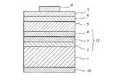
MOVPE法により形成したエピタキシャルウエハを用いると、これまで不可能であった短波長の発光や、高輝度が得られるLEDが作製できる。図5は従来のLEDの断面構造の一例を示す。このLEDは、n型GaAs基板1の第一の主面上に、n型AlGaInPクラッド層2/アンドープAlGaInP活性層3/p型AlGaInPクラッド層4からなるダブルヘテロ構造の発光部層12を有する。さらにp型クラッド層4上にp型GaP等からなる電流分散層5が形成され、その上に透明導電層6が形成されている。透明導電層6の表面の一部にはAu等からなる表面電極9(光取り出し側)が形成され、基板1の第二の主面全面にはAuGe合金等からなる電極10(基板側電極)が形成されている。
【0004】
この構造のLEDにより高輝度の発光を得るには、発光素子の表面電極9から発光素子に注入する電流を増大させる必要があるが、p型半導体からなる活性層3は一般に比抵抗が高いため、表面電極9から活性層3に注入される電流は電極9の近傍で密となる。電極9近傍の電流が密な部分に発光が集中するので、電流の局所的な集中を防止して高輝度なLEDを得るためには、発光部層における電流分布を均一化する必要がある。そのために低抵抗で発光波長に対して吸収の少ない物質からなる電流分散層を発光部層と電極との間に設けることが行なわれている。
【0005】
しかしながら電流分散層5に使用されているGaPはキャリア密度が余り高くなく、比較的高い比抵抗を有する。このため、十分な電流分散作用を得るには、GaP層を厚く成長させる必要がある。例えば、p型GaP(Znドープ量1×1018cm-3)の場合約50μm以上の膜厚とする必要がある。しかしGaP層を厚くするとLEDの製造コストが高くなる。
【0006】
LEDのコストを下げるには電流分散層を薄くできれば良いが、これには抵抗の低いエピタキシャル層が必要であり、高キャリア濃度層が求められている。しかしAlGaInPやGaNのような半導体材料では、p型で高キャリア濃度のエピタキシャル層を成長させることが難しい。また他にもこの条件を満たす半導体があれば良いが、そのような特性の半導体は発見されていない。
【0007】
そのため、低抵抗の電流分散層として種々の提案がなされている。その一つは、GaN系のLEDに金属薄膜を透明導電層として用いることである(特開平10-173224号)。しかしながら、金属薄膜の透光性を十分に高めるためには非常に薄くする必要があり、低抵抗でなくなる。一方、低抵抗を保持しようとすると、金属薄膜の膜厚には限界があり、透光性に劣るようになる。
【0008】
十分な透光性と十分な電流分散を得るのに必要な導電性とを満たす材料として、酸化インジウムスズ(ITO)のような金属酸化物が知られている。ITO膜を電流分散層として用いると、従来の厚い半導体電流分散層が不要になるので、低コストで高輝度のLEDが得られるようになる。光取り出し側の表面電極と発光部層との間にITO膜を設けたLEDの例は、米国特許5,481,122号、特開平11-4020号等に記載されている。
【0009】
しかしエピタキシャルウエハ上にITO膜が形成されたLEDでは、ダイシング等の工程で、ITO膜が剥離してしまうという問題が生じることが分かった。そのため、エピタキシャルウエハ上にITO膜を有するLEDの実用化は困難であった。そのため、ITOのような金属酸化物系透明導電層を使用しながらダイシング時のエピタキシャルウエハからの剥離の問題がない半導体発光素子の開発が望まれている。
【0010】
従って本発明の目的は、高輝度でダイシング等による透明導電層の剥離の問題がない半導体発光素子を提供することである。
【0011】
【課題を解決するための手段】
上記目的に鑑み鋭意研究の結果、本発明者等は、発光部層上(電流分散層及び/又は化合物半導体層が設けられている場合にはその上)に単層の透明導電層を形成する代わりに、組成の異なる2層以上の透明導電層を形成するか、組成が徐々に変化する透明導電層を形成することにより、ダイシング時の透明導電層の剥離を抑制できることを発見し、本発明に想到した。
【0012】
すなわち、本発明の第一の半導体発光素子は、第一導電型の基板に、第一導電型のクラッド層と第二導電型のクラッド層とに挟まれた活性層からなる発光部層と、金属酸化物からなる透明導電層と、電極とが形成され、前記透明導電層は2層以上の多層構造を有することを特徴とする。
【0013】
本発明の第二の半導体発光素子は、第一導電型の基板に、第一導電型のクラッド層と第二導電型のクラッド層とに挟まれた活性層からなる発光部層と、金属酸化物からなる透明導電層と、電極とが形成され、前記透明導電層は組成が徐々に変化する傾斜組成構造を有することを特徴とする。
【0014】
第一及び第二の半導体発光素子のいずれにおいても、前記発光部層と前記透明導電層との間に第二導電型の電流分散層及び/又は化合物半導体層が形成されていても良い。
【0015】
本発明の好ましい一実施例では、前記発光部層側の透明導電層はSnO2又はSb及びFの少なくとも1種の元素を含有するSnO2からなり、表面電極側の透明導電層はIn2O3又はSnドープIn2O3からなる。
【0016】
本発明の好ましい別の実施例では、前記発光部層側の透明導電層はZnO又はAl、In及びFからなる群から選ばれた少なくとも1種の元素を含有するZnOからなり、表面電極側の透明導電層はITOからなる。
【0017】
本発明の好ましいさらに別の実施例では、前記発光部層側の透明導電層はZn2SnO4からなり、表面電極側の透明導電層はITOからなる。
【0018】
本発明の好ましいさらに別の実施例では、前記発光部層側の透明導電層はTiO2からなり、表面電極側の透明導電層はITOからなる。
【0019】
基板はGaAsからなり、前記活性層はAlGaInP又はGaInPからなるのが好ましい。また前記電流分散層はGaP,GaAlP,GaAlAs,GaAsP,AlGaInP,AlInPからなる群から選ばれた少なくとも1種の化合物半導体からなるのが好ましい。
【0020】
前記化合物半導体層は、(1) InP又はInAsの二元系化合物半導体、(2) AlInAs又はAlInPの三元系化合物半導体、(3) AlGaAs、AlGaP、GaInAs及びGaInPからなる群から選ばれた少なくとも1種の三元系化合物半導体(Gaのモル比:0.2以下)、(4) AlInAsPの四元系化合物半導体、(5) AlGaInP、AlGaInAs、AlGaAsP及びGaInAsPからなる群から選ばれた少なくとも1種の四元系化合物半導体(Gaのモル比:0.2以下)、又は(6) AlGaInAsPからなる五元系化合物半導体(Gaのモル比:0.2以下)のいずれかである。
【0021】
【発明の実施の形態】
図1は本発明の一実施例による半導体発光素子の層構造を示す断面図である。この実施例では第一導電型はn型であり、第二導電型はp型であるが、この逆であっても良い。
【0022】
n型GaAs基板1の第一主面上にn型AlGaInPクラッド層2が形成され、このクラッド層2の上にアンドープAlGaInP活性層3が形成され、この活性層3の上にp型AlGaInPクラッド層4が形成されている。n型クラッド層2と、活性層3と、p型クラッド層4とはダブルヘテロ構造の発光部層12を構成している。図1の実施例では、発光部層12の上にp型電流分散層5が形成されているが、電流分散層5は必須ではない。透明導電層7の上には部分的にp型表面電極9が形成されており、また基板1の裏面にはn型裏面電極10が形成されている。
【0023】
発光部層12は、p-n接合型のダブルへテロ接合構造を有するAlGaInP混晶により構成される。特にインジウム組成比を約0.5とする(AlxGa1-x)0.5In0.5P(0≦x≦1)は、GaAs単結晶基板1と格子整合するため好ましい。各クラッド層2,4の厚さは好ましくは0.2〜3.0nmであり、より好ましくは0.3〜1.0nmである。また活性層3の厚さは好ましくは0.2〜1.0nmであり、より好ましくは0.6〜1.0nmである。
【0024】
p型電流分散層5は、通常p型のGaP、GaAlP,GaAsP,GaAlAs,AlGaInP,AlInPからなる群から選ばれた少なくとも1種の化合物半導体からなる。p型電流分散層5を構成する化合物半導体は、発光波長の吸収が少なく、比抵抗が低いことが必要である。一般に紅色〜橙色の発光ダイオードでは、電流分散層5はGaAlAsからなり、黄色〜緑色の発光ダイオードでは、電流分散層5はGaP又はGaAsPからなる。電流分散層5はできるだけ薄い方が好ましい。
【0025】
この実施例では、電流分散層5上に組成が異なる2層の透明導電層6,7が形成されている。勿論透明導電層の層数は2に限定されず、3以上でも良い。
透明導電層6,7の組合せとしては、(1) 透明導電層6が酸化錫(SnO2)又はSb及びFの少なくとも1種の元素を含有するSnO2からなり、透明導電層7がIn2O3又はSnドープ酸化インジウム(In2O3)からなる場合、(2) 透明導電層6が酸化亜鉛(ZnO)又はAl、In及びFからなる群から選ばれた少なくとも1種の元素を含有するZnOからなり、透明導電層7が酸化インジウム錫(ITO)からなる場合、(3) 透明導電層6が酸化亜鉛錫(Zn2SnO4)からなり、透明導電層7がITOからなる場合、及び(4) 透明導電層6が酸化チタン(TiO2)からなり、透明導電層がITOからなる場合がある。
【0026】
(1) の場合、透明導電層6がSb及びFの少なくとも1種の元素を含有するときには、その元素の含有量は透明導電層6全体を100原子%として1〜10原子%であるのが好ましい。また透明導電層7がSn含有するときには、その含有量は透明導電層7全体を100原子%として1〜10原子%であるのが好ましい。
【0027】
(2) の場合、透明導電層6がAl、In及びFからなる群から選ばれた少なくとも1種の元素を含有するときには、その元素の含有量は透明導電層6全体を100原子%として1〜10原子%であるのが好ましい。
【0028】
ITOの比抵抗は一般に約3×10⁻⁶Ωmであり、電流分散層5を形成するp形GaPの比抵抗の約百分の一である。従って、透明導電層7がITO又はそれに近い組成からなることにより、電流分散層5の厚さを大幅に減少することができる。
【0029】
透明導電層6,7は、スピンコータ等で塗布膜を形成後に熱処理する湿式法、又はスパッタリング法や各種の蒸着法等の乾式法により形成できる。
【0030】
p型表面電極9はワイヤボンディングに供され、n型裏面電極10はダイボンディングに供されるから、p型表面電極9及びn型裏面電極10には良好なボンディング特性、下層との良好なオーミック特性及び下層との密着性が要求される。そのため各電極9,10は複数の金属層により構成するのが好ましい。各電極9,10は酸化物層を有していても良い。さらに各電極9,10は最上層にAu、Al等のボンディング特性の良い金属層を有するのが好ましい。例えば、p型表面電極9にAuZn/Ni/Auの積層電極を使用し、n型裏面電極10にAuGe/Ni/Au積層電極を使用するのが好ましい。
【0031】
各電極9,10の金属層は抵抗加熱蒸着法、電子線加熱蒸着法等の蒸着法で形成することができる。さらに各電極9,10にオーミック性を付与するための熱処理(アロイング)を施しても良い。酸化物層は各種の公知の成膜方法で形成することができる。
【0032】
図2は本発明の別の実施例による半導体発光素子の層構造を示す断面図である。n型GaAs基板1、発光部層12(n型AlGaInPクラッド層2、アンドープAlGaInP活性層3及びp型AlGaInPクラッド層4)、及びp型電流分散層5、p型表面電極9及びn型裏面電極10については、図1の実施例の半導体発光素子と同じである。この半導体発光素子では、透明導電層8が徐々に変化する傾斜組成を有する。傾斜組成の場合でも、発光部層12側の面の組成(第一の組成)と表面電極9側の面の組成(第二の組成)には、上記と同様に、(1) SnO2(又はSb及びFの少なくとも1種の元素を含有するSnO2)/In2O3又はSnドープIn2O3、(2) ZnO(又はAl、In及びFからなる群から選ばれた少なくとも1種の元素を含有するZnO)/ITO、(3) Zn2SnO4/ITO、及び(4) TiO2/ITOの組合せがある。
【0033】
透明導電層8は、例えば第一の組成を有する第一のターゲットと第二の組成を有する第二のターゲットとを使用する交互スパッタリング法により形成することができる。透明導電層8の組成の変化率は、第一のターゲットでスパッタする時間と第二のターゲットでスパッタする時間との比を徐々に変化させることにより、適宜設定することができる。すなわち、まず第一のターゲットを100%使用して第一の組成のスパッタを行い、次いで第二のターゲットでスパッタする時間を徐々に増大させするとともに第一のターゲットでスパッタする時間を徐々に減少させ、最後に第二のターゲットを100%にしてスパッタを行なう。
【0034】
図3に示す半導体発光素子は、電流分散層5と透明導電層6との間に化合物半導体層11が形成されている以外、図1の半導体発光素子と同じである。また図4に示す半導体発光素子は、電流分散層5と透明導電層8との間に化合物半導体層11が形成されている以外、図2の半導体発光素子と同じである。
【0035】
いずれの場合も、化合物半導体層11は、(1) InP又はInAsの二元系化合物半導体、(2) AlInAs又はAlInPの三元系化合物半導体、(3) AlGaAs、AlGaP、GaInAs及びGaInPからなる群から選ばれた少なくとも1種であって、Gaのモル比が0.2以下である三元系化合物半導体、(4) AlInAsPの四元系化合物半導体、(5) AlGaInP、AlGaInAs、AlGaAsP及びGaInAsPからなる群から選ばれた少なくとも1種であって、Gaのモル比が0.2以下である四元系化合物半導体、又は(6) AlGaInAsPからなり、Gaのモル比が0.2以下である五元系化合物半導体により形成するのが好ましい。上記(3) 及び(5) のGa含有化合物半導体では、Gaの化合物半導体6全体に対するモル比を0.2以下とするのが好ましいが、これはGaのモル比が0.2以上になると、ダイシング時に透明導電層6のはがれが多くなっていくためである。Gaのより好ましいモル比は0〜0.15である。
【0036】
化合物半導体の種類及び化合物半導体層11の厚さ等は、半導体発光素子の発光波長及び輝度等の条件により適宜選択するのが好ましい。化合物半導体層11の厚さは、発光波長に対して透明性が劣る材料を用いた場合は、薄ければ薄いほど良い。透明性に優れた材料を用いた場合は、厚さは問わない。
【0037】
化合物半導体層11はエピタキシャル成長法、例えば有機金属気相成長法(M0VPE法)により形成できる。
【0038】
本発明の半導体発光素子は基板1とn型クラッド層2の間に、バッファ層(図示せず)及び分布ブラッグ反射層(DBR層、図示せず)を有してもよい。バッファ層はn型(Seドープ)GaAsにより形成することができる。またDBR層により活性層3からの光線の基板1による吸収を減少して、半導体発光素子の発光効率を高めることができる。
【0039】
【実施例】
本発明を以下の実施例によりさらに詳細に説明するが、本発明はそれらに限定されるものではない。
【0040】
実施例1
図1に示す構造を有する発光波長630 nm付近の赤色発光ダイオードチップを下記手順により作製した。
【0041】
まず700℃に加熱したn型GaAs基板1上に、厚さ500nmのn型(Seドープ)GaAsバッファ層、厚さ500nmのn型(Seドープ)(Al0.7Ga0.3)0.5In0.5Pクラッド層2(Seドープ量:1.0×1018cm-3)、厚さ600nmのアンドープ(Al0.15Ga0.85)0.5In0.5P活性層3、厚さ500nmのp型(亜鉛ドープ)(Al0.7Ga0.3)0.5In0.5Pクラッド層4(亜鉛ドープ量:5×1017cm-3)、及び厚さ2μmのp型(亜鉛ドープ)GaP電流分散層5(亜鉛ドープ量:5×1018cm-3)を、MOVPE法により順にエピタキシャル成長させた。p型AlGaInPからなるクラッド層4までのMOVPE成長は、700℃の温度及び50 Torrの圧力で、0.3〜1.0 nm/秒の成長速度で行なった。供給したV族元素とIII族元素の比(V/III比)は300〜600の範囲であった。またGaP層は、成長速度1nm/秒、V/III比100の条件で形成した。
【0042】
キャリアガスに水素を使用し、それぞれAl供給源としてトリメチルアルミニウム(TMA)、Ga供給源としてトリメチルガリウム(TMG)、In供給源としてトリメチルインジウム(TMI)、As供給源としてアルシン(AsH3)、P供給源としてホスフィン(PH3)、Zn供給源としてジエチル亜鉛(DEZ)、及びSe供給源としてH2Seを使用した。
【0043】
次いで、このエピタキシャルウェハ上にスパッタリング法により5%のSbを含有するSnO2からなる厚さ150nmの透明導電層6を形成し、さらにスパッタリング法により厚さ150nmの酸化インジウムスズ(ITO)からなる透明導電層7を形成した。透明導電層7上に、直径150μmの複数の円形開口部を有するマスクを使用して、厚さ60 nmの金−亜鉛合金、厚さ10 nmのニッケル、及び厚さ1000 nmの金を順に蒸着し、直径150μmの複数の円形p型表面電極9を透明導電層7の表面全体に等間隔に形成した。またn型GaAs基板1の底面全体に、厚さ60 nmの金−ゲルマニウム合金、厚さ10 nmのニッケル及び厚さ500 nmの金を順に蒸着し、n型の裏面電極10を形成した。
【0044】
このようにして作製した透明導電層6,7及び電極9,10付きのエピタキシャルウェハを、表面電極9を1つ含む300μm角のサイズでダイシングし、フレームに固定し、表面電極9にワイヤボンディングを、裏面電極10にダイボンディングを行なって、発光ダイオードチップを作製した。
【0045】
得られた発光ダイオードチップについて、透明導電層6,7がエピタキシャル層から剥離する不良を示す発光ダイオードチップの割合をチップ表面評価装置により調べたところ、全体の1%以下であった。
【0046】
実施例2
図2に示す構造を有する発光波長630 nm付近の赤色発光ダイオードチップを下記手順により作製した。実施例1と同じエピタキシャルウェハ(発光波長:630nm付近)を作製し、600℃に加熱しながら、SnO2からなる第一のターゲットとIn2O3からなる第二のターゲットとを交互に使用するスパッタリング法により、組成がSnO2からIn2O3に徐々に変化する厚さ300nmの透明導電層8を形成した。
【0047】
透明導電層8上に、直径150μmの複数の円形開口部を有するマスクを使用して、厚さ60 nmの金−亜鉛合金、厚さ10 nmのニッケル、及び厚さ1000 nmの金を順に蒸着し、直径150μmの複数の円形p型電極9を透明導電層8の表面全体に等間隔に形成した。またn型GaAs基板1の底面全体に、厚さ60 nmの金−ゲルマニウム合金、厚さ10 nmのニッケル及び厚さ500 nmの金を順に蒸着し、n型の裏面電極10を形成した。
【0048】
このようにして作製した透明導電層8及び電極9,10付きのエピタキシャルウェハを、表面電極9を1つ含む300μm角のサイズでダイシングし、フレームに固定したまま発光ダイオードの表面状態を調べたところ、透明導電層8がエピタキシャル層から剥離する不良を示す発光ダイオードは全体の1%であった。
【0049】
実施例3
実施例2と同じ条件で基板1上に、バッファ層、第一のクラッド層2、活性層3、第二のクラッド層4及び電流分散層5を、MOVPE法により順にエピタキシャル成長させた。得られたエピタキシャルウェハ上に、5%のSbを含有するSnO2からなる第一のターゲットとIn2O3からなる第二のターゲットとを使用する交互スパッタリング法により、組成がSb/SnO2からIn2O3に徐々に変化する厚さ300nmの透明導電層8を形成した。
【0050】
このようにして作製したエピタキシャルウェハに実施例1と同じ電極を形成した後、実施例1と同じ方法で発光ダイオードチップの表面状態を調べたところ、透明導電層8がエピタキシャル層から剥離する不良を示す発光ダイオードは全体の1%であった。
【0051】
比較例1
図5に示す構造を有する発光波長630nm付近の発光ダイオードを作製した。まず実施例1と同じ条件で基板1上に、バッファ層、第一のクラッド層2、活性層3、第二のクラッド層4及び電流分散層5を、MOVPE法により順にエピタキシャル成長させた。得られたエピタキシャルウエハ上に、スパッタリング法により厚さ300nmのITO膜(透明導電層6)を形成し、さらに両面に実施例1と同じ条件で電極9,10を形成した。
【0052】
このようにして作製した透明導電層(ITO)6及び電極9,10付きのエピタキシャルウェハを、表面電極9を1つ含む300μm角のサイズでダイシングし、フレームに固定したまま発光ダイオードチップの表面状態を調べたところ、透明導電層6がエピタキシャル層から剥離する不良を示す発光ダイオードは全体の90%以上であった。
【0053】
以上、ダブルヘテロ構造の発光部層12をAlGaInPにより形成した場合を例にとって説明したが、本発明はこれに限定される訳ではなく、例えばAlGaAsのような他の化合物半導体を発光部層12に用いる半導体発光素子にも適用可能である。また化合物半導体層11を有する半導体発光素子の場合、透明導電層の耐剥離性はさらに向上する。
【0054】
【発明の効果】
以上詳述したように、金属酸化物からなる透明導電層を異なる組成の二層以上の構造とするか、組成が徐々に変化する傾斜組成構造とするこれにより、透明導電層のエピタキシャルウエハからの剥離を著しく抑制することができる。これにより、半導体発光素子のエピタキシャルウエハの膜厚を従来の半導体発光素子よりも1/5〜1/10と薄くすることができ、輝度も約50%も向上することができる。
【図面の簡単な説明】
【図1】 本発明の一実施例による半導体発光素子を示す断面図である。
【図2】 本発明の別の実施例による半導体発光素子を示す断面図である。
【図3】 本発明のさらに別の実施例による半導体発光素子を示す断面図である。
【図4】 本発明のさらに別の実施例による半導体発光素子を示す断面図である。
【図5】 従来の半導体発光素子を示す断面図である。
【符号の説明】
1・・・基板
2・・・第1クラッド層
3・・・活性層
4・・・第2クラッド層
5・・・電流分散層
6・・・第一透明導電層
7・・・第二透明導電層
8・・・傾斜組成の透明導電層
9・・・表面電極
10・・・裏面電極
11・・・化合物半導体層
12・・・発光部層[0001]
BACKGROUND OF THE INVENTION
The present invention relates to a semiconductor light-emitting device having a transparent conductive layer, and more particularly to a semiconductor light-emitting device having a metal oxide-based transparent conductive layer having high brightness, low production cost, and no problem of peeling.
[0002]
[Prior art]
Conventional light emitting diodes (LEDs) are mostly GaP green light emitting diodes and AlGaAs red light emitting diodes. Recently, however, a technology for growing GaN-based and AlGaInP-based crystal layers by metal organic vapor phase epitaxy (MOVPE) has been developed, and high-intensity light-emitting diodes of orange, yellow, green, and blue can be manufactured.
[0003]
By using an epitaxial wafer formed by the MOVPE method, it is possible to produce an LED that can emit light with a short wavelength and high brightness, which has been impossible until now. FIG. 5 shows an example of a cross-sectional structure of a conventional LED. This LED has a light
[0004]
In order to obtain high-luminance light emission with an LED having this structure, it is necessary to increase the current injected from the surface electrode 9 of the light-emitting element into the light-emitting element, but the
[0005]
However, GaP used for the current spreading layer 5 does not have a very high carrier density and has a relatively high specific resistance. For this reason, in order to obtain a sufficient current dispersion action, it is necessary to grow the GaP layer thickly. For example, in the case of p-type GaP (Zn doping amount 1 × 1018 cm−3 ), the film thickness needs to be about 50 μm or more. However, thicker GaP layers increase the cost of LED manufacturing.
[0006]
In order to reduce the cost of the LED, it is sufficient if the current spreading layer can be made thin, but this requires an epitaxial layer with low resistance, and a high carrier concentration layer is required. However, it is difficult to grow a p-type high carrier concentration epitaxial layer with a semiconductor material such as AlGaInP or GaN. There are other semiconductors that satisfy this condition, but no semiconductor having such characteristics has been found.
[0007]
For this reason, various proposals have been made as a low-resistance current spreading layer. One of them is to use a metal thin film as a transparent conductive layer in a GaN-based LED (Japanese Patent Laid-Open No. 10-173224). However, in order to sufficiently increase the translucency of the metal thin film, it is necessary to make it very thin and the resistance is not low. On the other hand, when trying to maintain a low resistance, there is a limit to the thickness of the metal thin film, resulting in poor translucency.
[0008]
A metal oxide such as indium tin oxide (ITO) is known as a material satisfying sufficient translucency and conductivity necessary to obtain sufficient current dispersion. When an ITO film is used as a current spreading layer, a conventional thick semiconductor current spreading layer is not required, and a high-brightness LED can be obtained at low cost. Examples of LEDs in which an ITO film is provided between the surface electrode on the light extraction side and the light emitting layer are described in US Pat. No. 5,481,122, Japanese Patent Laid-Open No. 11-4020, and the like.
[0009]
However, it has been found that an LED having an ITO film formed on an epitaxial wafer has a problem that the ITO film is peeled off during a process such as dicing. For this reason, it has been difficult to put into practical use an LED having an ITO film on an epitaxial wafer. Therefore, it is desired to develop a semiconductor light emitting device that does not have a problem of peeling from an epitaxial wafer during dicing while using a metal oxide transparent conductive layer such as ITO.
[0010]
Accordingly, an object of the present invention is to provide a semiconductor light emitting device having high brightness and no problem of peeling of a transparent conductive layer due to dicing or the like.
[0011]
[Means for Solving the Problems]
As a result of intensive studies in view of the above object, the present inventors have formed a single transparent conductive layer on the light-emitting portion layer (if a current distribution layer and / or a compound semiconductor layer is provided). Instead, it was discovered that peeling of the transparent conductive layer during dicing can be suppressed by forming two or more transparent conductive layers having different compositions or by forming a transparent conductive layer whose composition gradually changes. I came up with it.
[0012]
That is, the first semiconductor light emitting device of the present invention comprises a light emitting part layer comprising an active layer sandwiched between a first conductive type cladding layer and a second conductive type cladding layer on a first conductive type substrate, A transparent conductive layer made of a metal oxide and an electrode are formed, and the transparent conductive layer has a multilayer structure of two or more layers.
[0013]
A second semiconductor light emitting device of the present invention includes a light emitting part layer comprising an active layer sandwiched between a first conductive type cladding layer and a second conductive type cladding layer on a first conductive type substrate, and a metal oxide layer. A transparent conductive layer made of a material and an electrode are formed, and the transparent conductive layer has a gradient composition structure in which the composition gradually changes.
[0014]
In any of the first and second semiconductor light emitting devices, a second conductivity type current spreading layer and / or compound semiconductor layer may be formed between the light emitting portion layer and the transparent conductive layer.
[0015]
In a preferred embodiment of the present invention, the transparent conductive layer of the light emitting portion layer side is made of SnO2 containing at least one element of SnO2 or Sb and F, the surface electrode side transparent conductive layer is In2 O3 or Sn-doped In2 O3 .
[0016]
In another preferred embodiment of the present invention, the transparent conductive layer on the light emitting layer side is made of ZnO or ZnO containing at least one element selected from the group consisting of Al, In and F, and is on the surface electrode side. The transparent conductive layer is made of ITO.
[0017]
In still another preferred embodiment of the present invention, the transparent conductive layer on the light emitting part layer side is made of Zn2 SnO4 and the transparent conductive layer on the surface electrode side is made of ITO.
[0018]
In still another preferred embodiment of the present invention, the transparent conductive layer on the light emitting part layer side is made of TiO2 , and the transparent conductive layer on the surface electrode side is made of ITO.
[0019]
The substrate is preferably made of GaAs, and the active layer is preferably made of AlGaInP or GaInP. The current spreading layer is preferably made of at least one compound semiconductor selected from the group consisting of GaP, GaAlP, GaAlAs, GaAsP, AlGaInP, and AlInP.
[0020]
The compound semiconductor layer is (1) a binary compound semiconductor of InP or InAs, (2) a ternary compound semiconductor of AlInAs or AlInP, and (3) at least selected from the group consisting of AlGaAs, AlGaP, GaInAs, and GaInP. One ternary compound semiconductor (Ga molar ratio: 0.2 or less), (4) AlInAsP quaternary compound semiconductor, (5) At least one selected from the group consisting of AlGaInP, AlGaInAs, AlGaAsP and GaInAsP Either a quaternary compound semiconductor (Ga molar ratio: 0.2 or less) or (6) a quaternary compound semiconductor (Ga molar ratio: 0.2 or less) made of AlGaInAsP.
[0021]
DETAILED DESCRIPTION OF THE INVENTION
FIG. 1 is a sectional view showing a layer structure of a semiconductor light emitting device according to an embodiment of the present invention. In this embodiment, the first conductivity type is n-type and the second conductivity type is p-type, but the opposite may be possible.
[0022]
An n-type
[0023]
The light emitting
[0024]
The p-type current spreading layer 5 is usually made of at least one compound semiconductor selected from the group consisting of p-type GaP, GaAlP, GaAsP, GaAlAs, AlGaInP, and AlInP. The compound semiconductor that constitutes the p-type current dispersion layer 5 needs to have low absorption of light emission wavelength and low specific resistance. In general, in a red to orange light emitting diode, the current spreading layer 5 is made of GaAlAs, and in a yellow to green light emitting diode, the current spreading layer 5 is made of GaP or GaAsP. The current spreading layer 5 is preferably as thin as possible.
[0025]
In this embodiment, two transparent
The combinations of the transparent
[0026]
In the case of (1), when the transparent conductive layer 6 contains at least one element of Sb and F, the content of the element is 1 to 10 atomic%, with the entire transparent conductive layer 6 being 100 atomic%. preferable. Further, when the transparent
[0027]
In the case of (2), when the transparent conductive layer 6 contains at least one element selected from the group consisting of Al, In and F, the content of the element is 1 with the entire transparent conductive layer 6 being 100 atomic%. It is preferably ˜10 atomic%.
[0028]
The specific resistance of ITO is generally about 3 × 10⁻⁶ Ωm, which is about one hundredth of the specific resistance of p-type GaP forming the current spreading layer 5. Therefore, when the transparent
[0029]
The transparent
[0030]
Since the p-type surface electrode 9 is used for wire bonding and the n-type back
[0031]
The metal layers of the
[0032]
FIG. 2 is a cross-sectional view illustrating a layer structure of a semiconductor light emitting device according to another embodiment of the present invention. n-type GaAs substrate 1, light emitting layer 12 (n-type AlGaInP clad
[0033]
The transparent
[0034]
The semiconductor light emitting device shown in FIG. 3 is the same as the semiconductor light emitting device of FIG. 1 except that a
[0035]
In any case, the
[0036]
The type of compound semiconductor and the thickness of the
[0037]
The
[0038]
The semiconductor light emitting device of the present invention may have a buffer layer (not shown) and a distributed Bragg reflection layer (DBR layer, not shown) between the substrate 1 and the n-
[0039]
【Example】
The present invention will be described in more detail with reference to the following examples, but the present invention is not limited thereto.
[0040]
Example 1
A red light-emitting diode chip having the structure shown in FIG.
[0041]
First, on an n-type GaAs substrate 1 heated to 700 ° C., an n-type (Se-doped) GaAs buffer layer having a thickness of 500 nm and an n-type (Se-doped) (Al0.7 Ga0.3 )0.5 In0.5 P cladding layer having a thickness of 500 nm 2 (Se doping amount: 1.0 × 1018 cm−3 ), 600 nm thick undoped (Al0.15 Ga0.85 )0.5 In0.5 P
[0042]
Hydrogen is used as the carrier gas, trimethylaluminum (TMA) as the Al supply source, trimethylgallium (TMG) as the Ga supply source, trimethylindium (TMI) as the In supply source, arsine (AsH3 ) as the As supply source, P Phosphine (PH3 ) was used as the source, diethyl zinc (DEZ) as the Zn source, and H2 Se as the Se source.
[0043]
Next, a transparent conductive layer 6 having a thickness of 150 nm made of SnO2 containing 5% Sb is formed on the epitaxial wafer by sputtering, and transparent made of indium tin oxide (ITO) having a thickness of 150 nm is further formed by sputtering. A
[0044]
The thus produced epitaxial wafer with transparent
[0045]
About the obtained light emitting diode chip | tip, when the ratio of the light emitting diode chip | tip which shows the defect which the transparent
[0046]
Example 2
A red light emitting diode chip having the structure shown in FIG. The same epitaxial wafer (emission wavelength: around 630 nm) as in Example 1 is manufactured, and the first target made of SnO2 and thesecond target made of In2 O3 are alternately used while heating to 600 ° C. A transparent
[0047]
A 60 nm thick gold-zinc alloy, 10 nm thick nickel, and 1000 nm thick gold are sequentially deposited on the transparent
[0048]
The epitaxial wafer with the transparent
[0049]
Example 3
A buffer layer, a
[0050]
After forming the same electrode as in Example 1 on the epitaxial wafer thus fabricated, the surface state of the light-emitting diode chip was examined by the same method as in Example 1. As a result, the transparent
[0051]
Comparative Example 1
A light emitting diode having a structure shown in FIG. First, a buffer layer, a
[0052]
The epitaxial wafer with the transparent conductive layer (ITO) 6 and the
[0053]
As described above, the case where the light emitting
[0054]
【The invention's effect】
As described in detail above, the transparent conductive layer made of a metal oxide has a structure of two or more layers having different compositions, or a gradient composition structure in which the composition gradually changes, whereby the transparent conductive layer can be removed from the epitaxial wafer. Peeling can be remarkably suppressed. Thereby, the film thickness of the epitaxial wafer of the semiconductor light emitting device can be reduced to 1/5 to 1/10 that of the conventional semiconductor light emitting device, and the luminance can be improved by about 50%.
[Brief description of the drawings]
FIG. 1 is a cross-sectional view showing a semiconductor light emitting device according to an embodiment of the present invention.
FIG. 2 is a cross-sectional view showing a semiconductor light emitting device according to another embodiment of the present invention.
FIG. 3 is a cross-sectional view illustrating a semiconductor light emitting device according to still another embodiment of the present invention.
FIG. 4 is a cross-sectional view showing a semiconductor light emitting device according to still another embodiment of the present invention.
FIG. 5 is a cross-sectional view showing a conventional semiconductor light emitting device.
[Explanation of symbols]
DESCRIPTION OF SYMBOLS 1 ...
10 ... Back electrode
11 ... Compound semiconductor layer
12 ... Light emitting layer
Claims (18)
Translated fromJapanesePriority Applications (1)
| Application Number | Priority Date | Filing Date | Title |
|---|---|---|---|
| JP2001154504AJP3697609B2 (en) | 2001-05-23 | 2001-05-23 | Semiconductor light emitting device |
Applications Claiming Priority (1)
| Application Number | Priority Date | Filing Date | Title |
|---|---|---|---|
| JP2001154504AJP3697609B2 (en) | 2001-05-23 | 2001-05-23 | Semiconductor light emitting device |
Publications (2)
| Publication Number | Publication Date |
|---|---|
| JP2002353499A JP2002353499A (en) | 2002-12-06 |
| JP3697609B2true JP3697609B2 (en) | 2005-09-21 |
Family
ID=18998834
Family Applications (1)
| Application Number | Title | Priority Date | Filing Date |
|---|---|---|---|
| JP2001154504AExpired - Fee RelatedJP3697609B2 (en) | 2001-05-23 | 2001-05-23 | Semiconductor light emitting device |
Country Status (1)
| Country | Link |
|---|---|
| JP (1) | JP3697609B2 (en) |
Families Citing this family (23)
| Publication number | Priority date | Publication date | Assignee | Title |
|---|---|---|---|---|
| JP2005005557A (en)* | 2003-06-13 | 2005-01-06 | Hitachi Cable Ltd | Manufacturing method of semiconductor light emitting device |
| JP3807394B2 (en)* | 2003-09-12 | 2006-08-09 | 日立電線株式会社 | Semiconductor light emitting device |
| KR100571818B1 (en) | 2003-10-08 | 2006-04-17 | 삼성전자주식회사 | Nitride-based light emitting device and its manufacturing method |
| WO2006006822A1 (en) | 2004-07-12 | 2006-01-19 | Gwangju Institute Of Science And Technology | Flip-chip light emitting diodes and method of manufacturing thereof |
| JP5220409B2 (en)* | 2004-07-23 | 2013-06-26 | 三星電子株式会社 | Method for manufacturing top-emitting nitride-based light emitting device |
| KR100682870B1 (en)* | 2004-10-29 | 2007-02-15 | 삼성전기주식회사 | Multi-layer electrode and compound semiconductor light emitting device having same |
| DE102005046190A1 (en) | 2005-09-27 | 2007-04-05 | Osram Opto Semiconductors Gmbh | Optoelectronic semiconductor device with current spreading layer |
| JP4137936B2 (en) | 2005-11-16 | 2008-08-20 | 昭和電工株式会社 | Gallium nitride compound semiconductor light emitting device |
| JP2007220972A (en)* | 2006-02-17 | 2007-08-30 | Showa Denko Kk | Semiconductor light emitting device, method for manufacturing the same, and lamp |
| JP2007220973A (en)* | 2006-02-17 | 2007-08-30 | Showa Denko Kk | Semiconductor light-emitting element, manufacturing method thereof, and lamp |
| JP5232968B2 (en)* | 2006-02-17 | 2013-07-10 | 豊田合成株式会社 | LIGHT EMITTING ELEMENT, ITS MANUFACTURING METHOD, AND LAMP |
| JP2008098486A (en)* | 2006-10-13 | 2008-04-24 | Kyocera Corp | Light emitting element |
| US8878245B2 (en) | 2006-11-30 | 2014-11-04 | Cree, Inc. | Transistors and method for making ohmic contact to transistors |
| TWI366291B (en)* | 2007-03-30 | 2012-06-11 | Epistar Corp | Semiconductor light-emitting device having stacked transparent electrodes |
| US9484499B2 (en) | 2007-04-20 | 2016-11-01 | Cree, Inc. | Transparent ohmic contacts on light emitting diodes with carrier substrates |
| US8368100B2 (en) | 2007-11-14 | 2013-02-05 | Cree, Inc. | Semiconductor light emitting diodes having reflective structures and methods of fabricating same |
| JP4909323B2 (en)* | 2008-07-25 | 2012-04-04 | 住友化学株式会社 | Active matrix substrate, display panel, display device, and method of manufacturing active matrix substrate |
| US7982232B2 (en) | 2008-08-27 | 2011-07-19 | Showa Denko K.K. | Semiconductor light-emitting device, manufacturing method thereof, and lamp |
| US8741715B2 (en) | 2009-04-29 | 2014-06-03 | Cree, Inc. | Gate electrodes for millimeter-wave operation and methods of fabrication |
| JP2009296007A (en)* | 2009-09-16 | 2009-12-17 | Sharp Corp | Group iii-v compound semiconductor light emitting element |
| JP6257203B2 (en)* | 2013-07-25 | 2018-01-10 | 晶元光電股▲ふん▼有限公司Epistar Corporation | Light emitting element |
| USD826871S1 (en) | 2014-12-11 | 2018-08-28 | Cree, Inc. | Light emitting diode device |
| JP2018037690A (en)* | 2017-12-05 | 2018-03-08 | 晶元光電股▲ふん▼有限公司Epistar Corporation | Light-emitting element |
- 2001
- 2001-05-23JPJP2001154504Apatent/JP3697609B2/ennot_activeExpired - Fee Related
Also Published As
| Publication number | Publication date |
|---|---|
| JP2002353499A (en) | 2002-12-06 |
Similar Documents
| Publication | Publication Date | Title |
|---|---|---|
| JP3697609B2 (en) | Semiconductor light emitting device | |
| US5317167A (en) | Semiconductor light-emitting device with InGaAlp | |
| CN100448041C (en) | Semiconductor light emitting element | |
| US20070122994A1 (en) | Nitride semiconductor light emitting element | |
| JP5169012B2 (en) | Semiconductor light emitting device | |
| JPH0897471A (en) | Group III nitride semiconductor light emitting device | |
| JPH0897468A (en) | Semiconductor light emitting device | |
| JP2012129357A (en) | Semiconductor light-emitting element | |
| JP2004186544A (en) | Semiconductor light emitting device | |
| JP2002368273A (en) | Semiconductor light emitting device | |
| JP2005005557A (en) | Manufacturing method of semiconductor light emitting device | |
| JP2002314131A (en) | Transparent electrode, manufacturing method thereof and group iii nitride semiconductor light emitting element using the same | |
| JP3504976B2 (en) | Semiconductor light emitting device | |
| JP4123360B2 (en) | Semiconductor light emitting device and manufacturing method thereof | |
| JP3700767B2 (en) | Semiconductor light emitting device | |
| JP2003046119A (en) | Light emitting diode and method of manufacturing the same | |
| US5235194A (en) | Semiconductor light-emitting device with InGaAlP | |
| JP2003101071A (en) | Semiconductor light emitting device | |
| WO2005038936A1 (en) | Light-emitting device and method for manufacturing same | |
| JP3763303B2 (en) | Semiconductor light emitting device | |
| JP3788444B2 (en) | Light emitting diode and manufacturing method thereof | |
| JP2003264313A (en) | Semiconductor light emitting device | |
| JPS62172766A (en) | Semiconductor light emitting device and its manufacturing method | |
| JP2001015805A (en) | AlGaInP-based light emitting device and epitaxial wafer for light emitting device | |
| JP3723314B2 (en) | Semiconductor light emitting device |
Legal Events
| Date | Code | Title | Description |
|---|---|---|---|
| A977 | Report on retrieval | Free format text:JAPANESE INTERMEDIATE CODE: A971007 Effective date:20050114 | |
| A131 | Notification of reasons for refusal | Free format text:JAPANESE INTERMEDIATE CODE: A131 Effective date:20050119 | |
| A521 | Written amendment | Free format text:JAPANESE INTERMEDIATE CODE: A523 Effective date:20050318 | |
| TRDD | Decision of grant or rejection written | ||
| A01 | Written decision to grant a patent or to grant a registration (utility model) | Free format text:JAPANESE INTERMEDIATE CODE: A01 Effective date:20050608 | |
| A61 | First payment of annual fees (during grant procedure) | Free format text:JAPANESE INTERMEDIATE CODE: A61 Effective date:20050621 | |
| R150 | Certificate of patent (=grant) or registration of utility model | Free format text:JAPANESE INTERMEDIATE CODE: R150 | |
| S531 | Written request for registration of change of domicile | Free format text:JAPANESE INTERMEDIATE CODE: R313531 | |
| R350 | Written notification of registration of transfer | Free format text:JAPANESE INTERMEDIATE CODE: R350 | |
| FPAY | Renewal fee payment (prs date is renewal date of database) | Free format text:PAYMENT UNTIL: 20090715 Year of fee payment:4 | |
| FPAY | Renewal fee payment (prs date is renewal date of database) | Free format text:PAYMENT UNTIL: 20100715 Year of fee payment:5 | |
| FPAY | Renewal fee payment (prs date is renewal date of database) | Free format text:PAYMENT UNTIL: 20100715 Year of fee payment:5 | |
| FPAY | Renewal fee payment (prs date is renewal date of database) | Free format text:PAYMENT UNTIL: 20110715 Year of fee payment:6 | |
| FPAY | Renewal fee payment (prs date is renewal date of database) | Free format text:PAYMENT UNTIL: 20120715 Year of fee payment:7 | |
| FPAY | Renewal fee payment (prs date is renewal date of database) | Free format text:PAYMENT UNTIL: 20130715 Year of fee payment:8 | |
| LAPS | Cancellation because of no payment of annual fees |