JP3695893B2 - Semiconductor device, manufacturing method and mounting method thereof - Google Patents
Semiconductor device, manufacturing method and mounting method thereofDownload PDFInfo
- Publication number
- JP3695893B2 JP3695893B2JP12993197AJP12993197AJP3695893B2JP 3695893 B2JP3695893 B2JP 3695893B2JP 12993197 AJP12993197 AJP 12993197AJP 12993197 AJP12993197 AJP 12993197AJP 3695893 B2JP3695893 B2JP 3695893B2
- Authority
- JP
- Japan
- Prior art keywords
- film
- semiconductor chip
- semiconductor device
- electrode pad
- external connection
- Prior art date
- Legal status (The legal status is an assumption and is not a legal conclusion. Google has not performed a legal analysis and makes no representation as to the accuracy of the status listed.)
- Expired - Fee Related
Links
Images


Classifications
- H—ELECTRICITY
- H01—ELECTRIC ELEMENTS
- H01L—SEMICONDUCTOR DEVICES NOT COVERED BY CLASS H10
- H01L23/00—Details of semiconductor or other solid state devices
- H01L23/48—Arrangements for conducting electric current to or from the solid state body in operation, e.g. leads, terminal arrangements ; Selection of materials therefor
- H01L23/488—Arrangements for conducting electric current to or from the solid state body in operation, e.g. leads, terminal arrangements ; Selection of materials therefor consisting of soldered or bonded constructions
- H01L23/495—Lead-frames or other flat leads
- H01L23/49572—Lead-frames or other flat leads consisting of thin flexible metallic tape with or without a film carrier
- H—ELECTRICITY
- H01—ELECTRIC ELEMENTS
- H01L—SEMICONDUCTOR DEVICES NOT COVERED BY CLASS H10
- H01L23/00—Details of semiconductor or other solid state devices
- H01L23/02—Containers; Seals
- H—ELECTRICITY
- H01—ELECTRIC ELEMENTS
- H01L—SEMICONDUCTOR DEVICES NOT COVERED BY CLASS H10
- H01L23/00—Details of semiconductor or other solid state devices
- H01L23/12—Mountings, e.g. non-detachable insulating substrates
- H01L23/13—Mountings, e.g. non-detachable insulating substrates characterised by the shape
- H—ELECTRICITY
- H01—ELECTRIC ELEMENTS
- H01L—SEMICONDUCTOR DEVICES NOT COVERED BY CLASS H10
- H01L25/00—Assemblies consisting of a plurality of semiconductor or other solid state devices
- H01L25/03—Assemblies consisting of a plurality of semiconductor or other solid state devices all the devices being of a type provided for in a single subclass of subclasses H10B, H10D, H10F, H10H, H10K or H10N, e.g. assemblies of rectifier diodes
- H01L25/10—Assemblies consisting of a plurality of semiconductor or other solid state devices all the devices being of a type provided for in a single subclass of subclasses H10B, H10D, H10F, H10H, H10K or H10N, e.g. assemblies of rectifier diodes the devices having separate containers
- H01L25/105—Assemblies consisting of a plurality of semiconductor or other solid state devices all the devices being of a type provided for in a single subclass of subclasses H10B, H10D, H10F, H10H, H10K or H10N, e.g. assemblies of rectifier diodes the devices having separate containers the devices being integrated devices of class H10
- H—ELECTRICITY
- H01—ELECTRIC ELEMENTS
- H01L—SEMICONDUCTOR DEVICES NOT COVERED BY CLASS H10
- H01L2224/00—Indexing scheme for arrangements for connecting or disconnecting semiconductor or solid-state bodies and methods related thereto as covered by H01L24/00
- H01L2224/01—Means for bonding being attached to, or being formed on, the surface to be connected, e.g. chip-to-package, die-attach, "first-level" interconnects; Manufacturing methods related thereto
- H01L2224/10—Bump connectors; Manufacturing methods related thereto
- H01L2224/15—Structure, shape, material or disposition of the bump connectors after the connecting process
- H01L2224/16—Structure, shape, material or disposition of the bump connectors after the connecting process of an individual bump connector
- H—ELECTRICITY
- H01—ELECTRIC ELEMENTS
- H01L—SEMICONDUCTOR DEVICES NOT COVERED BY CLASS H10
- H01L2224/00—Indexing scheme for arrangements for connecting or disconnecting semiconductor or solid-state bodies and methods related thereto as covered by H01L24/00
- H01L2224/01—Means for bonding being attached to, or being formed on, the surface to be connected, e.g. chip-to-package, die-attach, "first-level" interconnects; Manufacturing methods related thereto
- H01L2224/50—Tape automated bonding [TAB] connectors, i.e. film carriers; Manufacturing methods related thereto
- H—ELECTRICITY
- H01—ELECTRIC ELEMENTS
- H01L—SEMICONDUCTOR DEVICES NOT COVERED BY CLASS H10
- H01L2224/00—Indexing scheme for arrangements for connecting or disconnecting semiconductor or solid-state bodies and methods related thereto as covered by H01L24/00
- H01L2224/73—Means for bonding being of different types provided for in two or more of groups H01L2224/10, H01L2224/18, H01L2224/26, H01L2224/34, H01L2224/42, H01L2224/50, H01L2224/63, H01L2224/71
- H01L2224/732—Location after the connecting process
- H01L2224/73201—Location after the connecting process on the same surface
- H01L2224/73203—Bump and layer connectors
- H01L2224/73204—Bump and layer connectors the bump connector being embedded into the layer connector
- H—ELECTRICITY
- H01—ELECTRIC ELEMENTS
- H01L—SEMICONDUCTOR DEVICES NOT COVERED BY CLASS H10
- H01L2225/00—Details relating to assemblies covered by the group H01L25/00 but not provided for in its subgroups
- H01L2225/03—All the devices being of a type provided for in the same main group of the same subclass of class H10, e.g. assemblies of rectifier diodes
- H01L2225/10—All the devices being of a type provided for in the same main group of the same subclass of class H10, e.g. assemblies of rectifier diodes the devices having separate containers
- H01L2225/1005—All the devices being of a type provided for in the same main group of the same subclass of class H10, e.g. assemblies of rectifier diodes the devices having separate containers the devices being integrated devices of class H10
- H01L2225/1011—All the devices being of a type provided for in the same main group of the same subclass of class H10, e.g. assemblies of rectifier diodes the devices having separate containers the devices being integrated devices of class H10 the containers being in a stacked arrangement
- H01L2225/1017—All the devices being of a type provided for in the same main group of the same subclass of class H10, e.g. assemblies of rectifier diodes the devices having separate containers the devices being integrated devices of class H10 the containers being in a stacked arrangement the lowermost container comprising a device support
- H01L2225/1023—All the devices being of a type provided for in the same main group of the same subclass of class H10, e.g. assemblies of rectifier diodes the devices having separate containers the devices being integrated devices of class H10 the containers being in a stacked arrangement the lowermost container comprising a device support the support being an insulating substrate
- H—ELECTRICITY
- H01—ELECTRIC ELEMENTS
- H01L—SEMICONDUCTOR DEVICES NOT COVERED BY CLASS H10
- H01L2225/00—Details relating to assemblies covered by the group H01L25/00 but not provided for in its subgroups
- H01L2225/03—All the devices being of a type provided for in the same main group of the same subclass of class H10, e.g. assemblies of rectifier diodes
- H01L2225/10—All the devices being of a type provided for in the same main group of the same subclass of class H10, e.g. assemblies of rectifier diodes the devices having separate containers
- H01L2225/1005—All the devices being of a type provided for in the same main group of the same subclass of class H10, e.g. assemblies of rectifier diodes the devices having separate containers the devices being integrated devices of class H10
- H01L2225/1011—All the devices being of a type provided for in the same main group of the same subclass of class H10, e.g. assemblies of rectifier diodes the devices having separate containers the devices being integrated devices of class H10 the containers being in a stacked arrangement
- H01L2225/1041—Special adaptations for top connections of the lowermost container, e.g. redistribution layer, integral interposer
- H—ELECTRICITY
- H01—ELECTRIC ELEMENTS
- H01L—SEMICONDUCTOR DEVICES NOT COVERED BY CLASS H10
- H01L2225/00—Details relating to assemblies covered by the group H01L25/00 but not provided for in its subgroups
- H01L2225/03—All the devices being of a type provided for in the same main group of the same subclass of class H10, e.g. assemblies of rectifier diodes
- H01L2225/10—All the devices being of a type provided for in the same main group of the same subclass of class H10, e.g. assemblies of rectifier diodes the devices having separate containers
- H01L2225/1005—All the devices being of a type provided for in the same main group of the same subclass of class H10, e.g. assemblies of rectifier diodes the devices having separate containers the devices being integrated devices of class H10
- H01L2225/1011—All the devices being of a type provided for in the same main group of the same subclass of class H10, e.g. assemblies of rectifier diodes the devices having separate containers the devices being integrated devices of class H10 the containers being in a stacked arrangement
- H01L2225/1047—Details of electrical connections between containers
- H01L2225/1058—Bump or bump-like electrical connections, e.g. balls, pillars, posts
- H—ELECTRICITY
- H01—ELECTRIC ELEMENTS
- H01L—SEMICONDUCTOR DEVICES NOT COVERED BY CLASS H10
- H01L23/00—Details of semiconductor or other solid state devices
- H01L23/48—Arrangements for conducting electric current to or from the solid state body in operation, e.g. leads, terminal arrangements ; Selection of materials therefor
- H01L23/488—Arrangements for conducting electric current to or from the solid state body in operation, e.g. leads, terminal arrangements ; Selection of materials therefor consisting of soldered or bonded constructions
- H01L23/498—Leads, i.e. metallisations or lead-frames on insulating substrates, e.g. chip carriers
- H01L23/49811—Additional leads joined to the metallisation on the insulating substrate, e.g. pins, bumps, wires, flat leads
- H01L23/49816—Spherical bumps on the substrate for external connection, e.g. ball grid arrays [BGA]
- H—ELECTRICITY
- H01—ELECTRIC ELEMENTS
- H01L—SEMICONDUCTOR DEVICES NOT COVERED BY CLASS H10
- H01L23/00—Details of semiconductor or other solid state devices
- H01L23/48—Arrangements for conducting electric current to or from the solid state body in operation, e.g. leads, terminal arrangements ; Selection of materials therefor
- H01L23/488—Arrangements for conducting electric current to or from the solid state body in operation, e.g. leads, terminal arrangements ; Selection of materials therefor consisting of soldered or bonded constructions
- H01L23/498—Leads, i.e. metallisations or lead-frames on insulating substrates, e.g. chip carriers
- H01L23/4985—Flexible insulating substrates
- H—ELECTRICITY
- H01—ELECTRIC ELEMENTS
- H01L—SEMICONDUCTOR DEVICES NOT COVERED BY CLASS H10
- H01L2924/00—Indexing scheme for arrangements or methods for connecting or disconnecting semiconductor or solid-state bodies as covered by H01L24/00
- H01L2924/01—Chemical elements
- H01L2924/01078—Platinum [Pt]
- H—ELECTRICITY
- H01—ELECTRIC ELEMENTS
- H01L—SEMICONDUCTOR DEVICES NOT COVERED BY CLASS H10
- H01L2924/00—Indexing scheme for arrangements or methods for connecting or disconnecting semiconductor or solid-state bodies as covered by H01L24/00
- H01L2924/01—Chemical elements
- H01L2924/01079—Gold [Au]
- H—ELECTRICITY
- H01—ELECTRIC ELEMENTS
- H01L—SEMICONDUCTOR DEVICES NOT COVERED BY CLASS H10
- H01L2924/00—Indexing scheme for arrangements or methods for connecting or disconnecting semiconductor or solid-state bodies as covered by H01L24/00
- H01L2924/15—Details of package parts other than the semiconductor or other solid state devices to be connected
- H01L2924/151—Die mounting substrate
- H01L2924/153—Connection portion
- H01L2924/1531—Connection portion the connection portion being formed only on the surface of the substrate opposite to the die mounting surface
- H01L2924/15311—Connection portion the connection portion being formed only on the surface of the substrate opposite to the die mounting surface being a ball array, e.g. BGA
Landscapes
- Engineering & Computer Science (AREA)
- Microelectronics & Electronic Packaging (AREA)
- Power Engineering (AREA)
- Physics & Mathematics (AREA)
- Condensed Matter Physics & Semiconductors (AREA)
- General Physics & Mathematics (AREA)
- Computer Hardware Design (AREA)
- Wire Bonding (AREA)
- Structures Or Materials For Encapsulating Or Coating Semiconductor Devices Or Solid State Devices (AREA)
- Encapsulation Of And Coatings For Semiconductor Or Solid State Devices (AREA)
- Lead Frames For Integrated Circuits (AREA)
Abstract
Description
Translated fromJapanese【0001】
【発明の属する技術分野】
本発明は、半導体チップとほぼ同じ大きさであり、特に多出力の半導体チップに適するパッケージを有する半導体装置と、その製造方法および実装方法に関するものである。
【0002】
【従来の技術】
従来、この種の半導体チップとほぼ同じ大きさのパッケージは、チップサイズパッケージ、μ−BGA、チップスケールパッケージ、CSP等と称され、さまざまなタイプのものが開発されている。図24は従来のモールドタイプのパッケージを有する半導体装置の一部破断斜視図である。この半導体装置は、LSIチップ241の電極パッドにバンプ242を形成し、次にトランスファー成形金型を用いて、略LSIと同じ大きさのモールド樹脂243により樹脂封止し、最後に外部電極に半田ボール244を搭載することにより製造される。
【0003】
また、図25は従来のフィルム(フィルムキャリアテープ)タイプのパッケージを有する半導体装置の断面図である。この半導体装置は、LSIチップ251の表面に弾性接着剤(エラストマ)252をコーティングし、インナーリード253および外部接続パッド254が形成されたポリイミドフィルム255を弾性接着剤252によりLSIチップ251表面に固定し、LSIチップ251のチップ電極パッドにインナーリード253をボンディングし、外部接続パッド254に半田ボール256を搭載することにより製造される。
【0004】
また、図26は従来のフリップチップボンディングタイプのパッケージを有する半導体装置の断面図である。この半導体装置は、LSIチップ261の表面にバンプ262を形成し、次にLSIチップ261をセラミックまたは有機系材料の基板263にフェースダウンボンディングし、次に封止樹脂264を用いて封止することにより製造される。基板263の裏面には半田ボール265が搭載される。図24〜図26に示すいずれのタイプのパッケージを用いても、略LSIと同じ大きさのパッケージを有する半導体装置を製造することができる。
【0005】
【発明が解決しようとする課題】
しかしながら、図24に示す半導体装置では、専用のトランスファー金型を必要とし、このことが低価格化の障害となっていた。
【0006】
また、図25に示す半導体装置では、LSIチップとテープの中間に特殊な弾性接着剤を用いるため、LSIチップ表面の汚染やダメージ等が発生し、信頼性が劣化する恐れがあった。またLSΙチップとインナーリードを接続する際に、にリードを一本ずつボンディングするシングルポイントボンディングを用いており、多出力パッケージにおいてはボンディング時間が長くなり、低価格化の障害となっていた。
【0007】
また、図26に示す半導体装置では、多出力パッケージにおいては基板が多層で高価格となり、またサイズの大きいLSIチップにおいては基板とLSΙチップの熱膨張差により、信頼性上問題になることがあった。
【0008】
本発明は、このような従来の問題を除去するものであり、多出力のLSIチップを用いる場合に好適な、低価格かつ高信頼性の半導体装置とその製造方法および実装方法を提供することを目的とする。
【0009】
【課題を解決するための手段】
上記の目的を達成するために本発明の請求項1記載の半導体装置は、半導体チップが実装されたデバイス実装フィルム部と、前記デバイス実装フィルム部上に配置され、外部電極パッドが形成された外部接続フィルム部と、前記デバイス実装フィルム部の端部と前記外部接続フィルム部の端部との間に設けられた折曲部と、前記折曲部を経由して前記半導体チップの電極パッドと前記外部電極パッドとを電気的に接続するインナーリードとを有するパッケージフィルムと、底板と天板からなるコの字板とを備え、前記コの字板内面に前記デバイス実装フィルム部を取り付け、前記天板外面に前記外部接続フィルム部を取り付けたことを特徴とする。
【0010】
請求項2記載の半導体装置は、チップの中央部あるいはチップの中心線に沿った領域にパッド電極が配置された半導体チップが実装されたパッケージフィルムを備え、前記パッケージフィルムが、前記半導体チップのパッド電極形成領域に対応して、中央部あるいは中心線に沿った領域に形成されたデバイスホールと、前記デバイスホールの形成領域以外の領域に形成された外部電極パッドと、前記半導体チップの電極パッドと前記外部電極パッドとを接続するインナーリードとを有するとともに、前記半導体チップの実装面に絶縁性の樹脂突起を有することを特徴とする。
【0011】
請求項3記載の半導体装置は、チップの周辺部にパッド電極が配置された半導体チップが実装されたパッケージフィルムを備え、前記パッケージフィルムが、前記半導体チップのパッド電極形成領域に対応して、周辺部に形成されたデバイスホールと、前記デバイスホールの形成領域以外の領域に形成された外部電極パッドと、前記半導体チップのパッド電極と前記外部電極とを接続するインナーリードとを有するとともに、前記半導体チップの実装面に絶縁性の樹脂突起を有し、前記パッケージフィルムと前記半導体チップの表面との間を封止樹脂により固定したことを特徴とする。
【0012】
請求項4記載の半導体装置は、所定の領域に電極パッドが配置された半導体チップの表面と対面するように、前記半導体チップが実装されたデバイス実装フィルム部と、前記半導体チップの裏面に配置され、外部電極パッドが形成された外部接続フィルム部と、前記デバイス実装フィルム部の端部と前記外部接続フィルム部の端部との間に設けられた折曲部と、インナーリードとを有するパッケージフィルムを備え、前記デバイス実装フィルム部が、前記半導体チップのパッド電極形成領域に対応して、所定の領域に形成されたデバイスホールと、前記デバイスホールの形成領域以外の領域に形成された外部電極パッドとを有し、前記インナーリードが、前記半導体チップの電極パッドと前記デバイス実装フィルム部の外部電極パッドとを電気的に接続するとともに、前記折曲部を経由して前記半導体チップの電極パッドと前記外部接続フィルム部とを電気的に接続することを特徴とする。
【0013】
請求項8記載の半導体装置は、請求項4記載の半導体装置において、前記パッケージフィルムが、前記半導体チップの実装面に絶縁性の樹脂突起を有することを特徴とする。また、請求項9記載の半導体装置は、請求項4記載の半導体装置において、前記パッケージフィルムが、前記折曲部を複数有し、前記複数の折曲部にそれぞれ対応して、前記外部接続フィルム部を複数有することを特徴とする。また、請求項12記載の半導体装置は、請求項4記載の半導体装置において、前記折曲部が、前記インナーリードを弾性樹脂によりコーティングした構造を有することを特徴とする。また、請求項13記載の半導体装置は、請求項4記載の半導体装置において、前記インナーリードが、前記半導体チップの電極パッドに直接ボンディングされていることを特徴とする。
【0014】
次に、本発明の請求項16記載の半導体装置の製造方法は、チップの中央部あるいはチップの中心線に沿った領域に電極パッドが配置された半導体チップと、前記半導体チップの電極パッド形成領域に対応して、中央部あるいは中心線に沿った領域にデバイスホールが形成され、前記デバイスホール形成領域以外の領域の外部接続面側に外部電極パッドが形成され、前記デバイスホールから前記外部電極に至るようにインナーリードが形成されたパッケージフィルムとを用い、前記デバイスホール形成領域において前記インナーリードを半導体チップの電極パッドにボンディングして、前記半導体チップを前記パッケージフィルムのデバイス実装面側に実装する工程を実施し、前記パッケージフィルムは、デバイス実装面側に絶縁性の樹脂突起が形成されたものであり、前記半導体チップの実装工程は、インナーリードをボンディングしてから、前記パッケージフィルムと前記半導体チップとの空間に封止樹脂を流し込んで、前記半導体チップを前記パッケージフィルムに固定するものであることを特徴とする。
【0015】
請求項17記載の製造方法は、チップの周辺部に電極パッドが配置された半導体チップと、前記半導体チップのパッド電極形成領域に対応して、周辺部にデバイスホールが形成され、前記デバイスホール形成領域以外の領域の外部接続面側に外部電極パッドが形成され、前記デバイスホールから前記外部電極に至るようにインナーリードが形成されたパッケージフィルムとを用い、前記デバイスホール形成領域において前記インナーリードを半導体チップの電極パッドにボンディングし、前記パッケージフィルムと前記半導体チップ表面の間に封止樹脂を流し込んで、前記半導体チップを前記パッケージフィルムのデバイス実装面側に実装する工程を実施し、前記半導体チップの実装工程は、インナーリードをボンディングしてから、前記パッケージフィルムと前記半導体チップとの空間に封止樹脂を流し込んで、前記半導体チップを前記パッケージフィルムに固定するものであることを特徴とする。
【0016】
請求項18記載の製造方法は、所定の領域に電極パッドが配置された半導体チップと、前記半導体チップのパッド電極形成領域に対応して、所定の領域にデバイスホールが形成されたデバイス実装フィルム部と、外部接続フィルム部と、前記デバイス実装フィルム部と前記外部接続フィルム部の間に位置する折曲部とに領域分割される平面形状を有し、第1面側の前記外部接続フィルム部および第1面側の前記デバイス実装フィルム部のデバイスホール形成領域以外の領域に外部電極パッドが形成され、前記デバイスホールから前記それぞれの外部電極パッドに至るようにインナーリードが形成されたパッケージフィルムとを用い、前記デバイスホール形成領域において前記インナーリードを前記半導体チップ表面の電極パッドにボンディングし、第2面側の前記デバイス実装フィルム部に前記半導体チップを実装する工程と、前記外部接続フィルム部を折曲部にて前記半導体チップの裏面側に180゜折り曲げ、前記裏面に固定する工程とを順次実施することを特徴とする。
【0017】
請求項19記載の製造方法は、請求項18記載の製造方法において、前記デバイス実装フィルム部が、第2面側に絶縁性の樹脂突起が形成されたものであり、前記半導体チップの実装工程が、インナーリードをボンディングしてから、前記デバイス実装フィルム部と前記半導体チップとの空間に封止樹脂を流し込んで、前記半導体チップを前記デバイス実装フィルム部の第2面に固定するものであることを特徴とする。また、請求項22記載の製造方法は、請求項18記載の製造方法において、前記パッケージフィルムが、前記折曲部を複数有するとともに、前記複数の折曲部にそれぞれ対応して、前記外部接続フィルム部を複数有し、前記外部接続フィルム部を固定する工程が、前記複数の外部接続フィルム部を、対応する折曲部においてそれぞれ前記半導体チップの裏面側に180゜折り曲げ、前記裏面に固定するものであることを特徴とする。
【0018】
請求項28記載の製造方法は、請求項18記載の製造方法において、前記半導体チップの実装工程が、前記インナーリードを前記半導体チップの電極パッドに一括ボンディングするものであることを特徴とする。また、請求項29記載の製造方法は、請求項18記載の製造方法において、前記半導体チップのパッド電極に前記インナリードを直接ボンディングすることを特徴とする。
【0019】
次に、本発明の請求項30記載の半導体装置の実装方法は、請求項1ないし14のいずれかに記載の半導体装置をマザーボードに密着実装する半導体装置の実装方法であって、前記マザーボードの電極パッドに半田ボールを搭載し、このマザーボード上に前記半導体装置を載置し、前記半田ボールを溶解させて、前記マザーボードの電極パッドと前記半導体装置の外部電極パッドとを電気的に接続することを特徴とする。
【0020】
請求項31記載の半導体装置の実装方法は、請求項4記載の半導体装置を複数積層してマザーボードに実装する半導体装置の実装方法であって、前記マザーボードの電極パッドに、第1の半導体装置の外部接続フィルム部またはデバイス実装フィルム部のいずれか一方に形成された外部電極パッドを重ね、さらに第1の半導体装置の他方のフィルム部に形成された外部電極パッドに、第2の半導体装置の外部接続フィルム部またはデバイス実装フィルム部のいずれか一方に形成された外部電極パッドを重ね、前記重なり合った電極どうしを電気的に接続することを特徴とする。
【0021】
【発明の実施の形態】
第1の実施形態
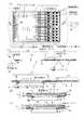
図1は本発明の第1の実施形態の半導体装置の構造および製造工程を示す図である。図1において、(a)はこの半導体装置に用いられるパッケージフィルム1をインナーリード形成面(第1面)1Aから見た上面図、(b)は(a)のA−A’間の断面図、(c)および(d)は第1の実施形態の半導体装置の製造途中における断面構造図、(e)は第1の実施形態の半導体装置の断面構造図である。
【0022】
まず、図1(a)および(b)に示すように、パッケージフィルム1を作成する。すなわち、プレスパンチング加工により、デバイス実装フィルム部予定領域にデバイスホール12が形成され、折曲部予定領域に折曲ホール13が形成されたポリイミドのベース樹脂2に、インナーリード3を形成する。ここで、インナーリード3は、例えば、ベース樹脂2の表面に銅箔を貼り付け、この銅箔をフォトリソエッチングによりパターニングし、半田またはスズをメッキ処理したものである。尚、図中の3aはダミーインナーリードである。次に、この上に絶縁樹脂4をコーティングし、フォトリソエッチングにより、絶縁樹脂4に電極パッドホール4aを開孔してインナーリード3を露出させ、外部電極パッド5を形成する。尚、印刷法により絶縁樹脂4を選択的にコーティング(パターニング)して、外部電極パッド5を形成しても良い。また、インナーリード3の強度劣化あるいは断線を防止することを目的として、折曲部1dにおけるインナーリード3の片面または両面にポリイミド系の弾性樹脂6をコーティングすることが望ましい。以上により、パッケージフィルム1が作成される。尚、TAB(Tape Automated Bonding)製造技術を用いる場合には、パッケージフィルム1は、フィルムキャリアテープ1aに複数作り込まれて供給される。
【0023】
次に、図1(c)に示すように、パッケージフィルム1のインナーリード形成面1A(第1面)をLSΙチップ8の表面に対面させて、パッケージフィルム1のデバイス実装フィルム部1bにLSΙチップ8を実装する。すなわち、パッケージフィルム1のデバイス実装フィルム部1bにおいて、金メッキ等が施されたバンプ7が形成されたLSΙチップ8のチップ電極パッド8aに、熱圧着法によりインナーリード3およびダミーインナーリード3aを一括ボンディングし、デバイス実装フィルム部1bとLSΙチップ8の表面とにより形成される空間にエポキシ樹脂等の封止樹脂9を流し込み、デバイス実装フィルム部1bに対してLSΙチップ8を固定実装する。ここで、ボンディングされたダミーインナーリード3aは、インナーリード3がボンディングされてからLSΙチップ8が固定されるまでに、インナーリード3が断線したり、ボンディング部が剥離することを防止する機能を有する。尚、TAB技術を用いる場合には、LSΙチップ8の実装終了後に、パンチング加工によりフィルムキャリアテープ1aからパッケージフィルム1を分離する。
【0024】
次に、図1(d)に示すように、パッケージフィルム1の外部接続フィルム部1cを、折曲部1dにてベース樹脂面1B(第2面)側に180゜折り曲げ、接着剤10によってデバイス実装フィルム部1bにおける封止樹脂9表面に固定する。ここで折り曲げるポイントは、例えばLSIチップ8の側面の外側約1[mm]程度の所とする。最後に図1(e)に示すように、外部電極パッド5に半田ボール11を搭載する。
【0025】
このように第1の実施形態によれば、デバイス実装フィルム部1bのデバイスホール12に突き出して形成されたインナーリード3(およびダミーインナーリード3a)をLSIチップ8のチップ電極パッド8aに一括ボンディングしてLSIチップ8をデバイス実装フィルム部1bに実装し、外部接続フィルム部1cを折曲部1d(LSIチップ8の外側約1[mm])を境にして180゜折曲げ、デバイス実装フィルム部1bに固定することにより、特殊な弾性接着剤を用いないので信頼性を向上させることができ、また専用のトランスファー金型を用いず、インナーリードをLSIチップに一括ボンディングするので、製造コストを低減することができ、従って低価格化を図ることができる。
【0026】
尚、図1(e)に示す工程を実施せずに、図1(d)に示すように、外部電極パッド5に半田ボール11が搭載されていない構造としても良い。このチップサイズパッケージをマザーボードに実装する際は、マザーボード側に半田ボールを供給することにより良好な接続が可能である。マザーボードへの半田ボールの供給には、例えば印刷技術を用いる。このようにマザーボード側に半田ボールを供給することにより、複数のパッケージを同時に実装することが可能となるので、パッケージのマザーボードに対する実装工数を削減することができ、またパッケージの製造工程においては、外部電極パッドに半田ボールを搭載する工程が不要となるので、加工工数を削減でき、半導体装置の低価格化をさらに図ることができる。
【0027】
第2の実施形態
第2の実施形態は、ベース樹脂をプレスパンチング加工して外部電極パッドを形成することを特徴とするものである。図2は本発明の第2の実施形態の半導体装置の構造および製造工程を示す図である。図2において、(a)はこの半導体装置に用いられるパッケージフィルム21の断面図であり、(b)は第2の実施形態の半導体装置の断面構造図である。
【0028】
まず、図2(a)に示すように、パッケージフィルム21を形成する。すなわち、ベース樹脂2をプレスパンチング加工して、デバイスホール12、折曲ホール13、および外部電極パッド22となる電極パッドホール2aを形成する。次に、第1の実施形態と同じ手順で、この樹脂テープ2にインナーリード3およびダミーインナーリード3aを形成し、絶縁樹脂4をコーティングする。また、折曲部21dに弾性樹脂6をコーティングすることが望ましい。以上により、ベース樹脂面21B(第1面)側に開孔した外部電極パッド22を有するパッケージフィルム21が作成される。
【0029】
次に、図2(b)に示すように、ベース樹脂面21BをLSΙチップ8側にしてパッケージフィルム21のデバイス実装フィルム部21bにLSΙチップ8を実装する。すなわち、上記第1の実施形態と同じ手順で、バンプ7が形成されたLSΙチップ8のチップ電極パッド8aにインナーリード3およびダミーインナーリード3aをボンディングし、封止樹脂9によりLSΙチップ8をデバイス実装フィルム部21bに固定実装し、さらに外部接続フィルム部21cを、折曲部21dにてインナーリード形成面21A(第2面)側に180゜折り曲げ、接着剤10によりデバイス実装フィルム部21bの封止樹脂9表面に固定し、最後に外部電極パッド22に半田ボール11を搭載する。
【0030】
このように第2の実施形態によれば、パッケージフィルムの作成工程において、デバイスホール12等のプレスパンチング加工時に外部電極パッドホール2aを形成しておき、この外部電極パッドホール2a上にインナーリード3をパターニングして外部電極パッド22を形成することにより、パッケージフィルムの作成工数(絶縁樹脂のフォトリソエッチングの加工工数)を削減でき、材料費(絶縁樹脂)を削減できるので、さらに半導体装置の低価格化を図ることができる。
【0031】
尚、図2(b)において、外部電極パッド22に半田ボール11を搭載しない構造としても良い。
【0032】
第3の実施形態
第3の実施形態は、バンプを形成しないでインナーリードをLSIチップの電極パッドに直接ボンディングすることを特徴とするものである。図3は本発明の第3の実施形態の半導体装置の断面構造図であり、(a)は全体断面図、(b)は(a)の領域Eの部分断面図を示す。尚、下記以外の構造および製造工程は、上記第1の実施形態と同じである。
【0033】
図3において、インナーリード31は、銅箔31aに金メッキ31bを施し、150℃、30分程度のアニール処理をしたものである(ダミーインナーリードも同じである)。インナーリード31およびダミーインナーリードは、LSIチップ8のチップ電極パッド8aにバンプを介さずに熱圧着法により直接一括ボンディングされる。
【0034】
通常、バンプがないとLSIチップの電極パッドのダメージが大きく、パッド下にクラック等が発生する。しかしながら、銅箔31aに金メッキ31bを施したインナーリード31は、アニール処理等によりその硬度を下げることができるので、この軟化したインナーリード31を用いることによりチップ電極パッドへのダメージを緩和し、パッド下にクラック等が発生しない直接ボンディングが可能となる。
【0035】
このように第3の実施形態によれば、LSIチップの電極パッドにバンプを形成する工程が不要となるので、製造コストを削減でき、低価格化を図ることができる。
【0036】
尚、この第3の実施形態は、上記第2の実施形態に対しても適用可能であることは言うまでもない。また外部電極パッド5に半田ボール11を搭載しない構造としても良い。
【0037】
第1の参考例
第1の参考例は、LSIチップの側面および裏面を保護するための保護枠を設けたことを特徴とするものである。図4は第1の参考例の半導体装置を示す断面構造図である。図4に示す半導体装置は、上記第1の実施形態の半導体装置に、図4(a)に示す箱型の保護枠41、あるいは図4(b)に示す底部がない保護枠42を取り付けたものである。保護枠41はLSIチップ8の側面および裏面を覆うように取り付けられ、また保護枠42はLSIチップ8の側面を覆うように取り付けらている。これらの保護枠41、42は、樹脂、金属等の絶縁材料または導電性材料を成形加工したものであり、パッケージフィルム1のデバイス実装フィルム部1bに接着剤10bを用いて固定される。
【0038】
このように第1の参考例によれば、保護枠41または42を取り付けることにより、LSIチップ8の側面および裏面を保護することができるので、ハンドリング時にLSIチップ8の側面およびチップ裏面の欠けが発生しなくなり、実装時の歩留まり向上が期待できる。
【0039】
尚、この第1の参考例は、上記第2の実施形態または上記第3の実施形態に対しても適用可能であることは言うまでもない。また外部電極パッド5に半田ボール11を搭載しない構造としても良い。
【0040】
第2の参考例
第2の参考例は、外部接続フィルム部の平坦性を向上させるための平板を設けたことを特徴とするものである。図5は第2の参考例の半導体装置の断面構造図である。図5に示す半導体装置は、上記第1の実施形態の半導体装置において、パッケージフィルム1のデバイス実装フィルム部1bと外部接続フィルム部1cの間に、絶縁材料または金属等の導電性材料からなる平板51を取り付けたものである。この平板51は、接着剤10aおよび10bを用いてデバイス実装フィルム部1bの封止樹脂9表面と外部接続フィルム部1cとの間に固定される。平板51の取り付け手順としては、例えば、図1(b)に示す工程終了後に、接着剤10aにより平板51をデバイス実装フィルム部1bの封止樹脂9形成部上に固定し、次に外部接続フィルム部1cを180°折り曲げ、平板51上に接着剤10bにより固定する。
【0041】
このように第2の参考例によれば、デバイス実装フィルム部1bと外部接続フィルム部1cの間に平板51を取り付けることにより、外部接続フィルム部1cおよび半田ボール11の平坦性を向上させることができるので、マザーボードへの実装性を向上させることができる。また平板として金属板等を用いた場合には、半導体装置の熱放散性を向上させることができる。
【0042】
尚、この第2の参考例は、上記第2の実施形態、第3の実施形態、または第1の参考例に対しても適用可能であることは言うまでもない。また外部電極パッド5に半田ボール11を搭載しない構造としても良い。
【0043】
第4の実施形態
第4の実施形態は、外部接続フィルム部の平坦性を向上させるとともに、LSIチップの裏面を保護するコの字板を設けたことを特徴とするものである。図6は本発明の第4の実施形態の半導体装置の断面構造図である。図6に示す半導体装置は、上記第1の実施形態の半導体装置に、絶縁材料または金属等の導電性材料からなる、コの字型に成形加工されたコの字板61を取り付けたものである。コの字板61の底板61aのコの字内面には、LSIチップ8が取り付けられ(従ってデバイス実装フィルム部1bおよびLSIチップ8は底板61aと天板61bの間に位置する)、天板61bのコの字外面には、外部接続フィルム部1cが取り付けられている。コの字板61の装着手順としては、例えば、図1の(b)に示す工程を終了後に、LSIチップ8の底面を接着剤10aを用いて底板61aに固定し、次に外部接続フィルム部1cを180°折り曲げ、接着剤10bを用いて天板61bに固定する。あるいは、コの字板61として金属板等を用いる場合には、平板にLSIチップ8を固定し、次にこの平板を180゜折り返してコの字板61を形成し、最後に外部接続部1cを180゜折り曲げ、天板61bに固定する。尚、図6においては、パッケージフィルム1の折曲部1dの内面の向き(右から左)とコの字板61の湾曲部61cの内面の向き(左から右)とは180゜異なる位置関係にあるが、これを90゜異なる位置関係としても良い。
【0044】
このように第4の実施形態によれば、コの字板61を用い、その底板61aの内面にLSIチップ8を取り付け、天板61bの外面に外部接続フィルム部1cを取り付けることにより、外部接続フィルム部1cおよび半田ボール11の平坦性を向上させることができ、またLSIチップを保護することができる。またコの字板61として金属板等を用いた場合には、パッケージの熱放散性をさらに向上させることができる。
【0045】
尚、この第4の実施形態は、上記第2の実施形態または第3の実施形態に対しても適用可能であることは言うまでもない。また外部電極パッド5に半田ボール11を搭載しない構造としても良い。
【0046】
第3の参考例
第3の参考例は、外部接続フィルム部を2層両面導電層構造とすることを特徴とするものである。図7は第3の参考例の半導体装置の構造および製造工程を示す図である。
【0047】
まず、図7(a)に示すように、外部接続フィルム部71bに基準電源(接地電源)用のスルーホール2bを有するパッケージフィルム71を作成する。すなわち、ベース樹脂2にデバイスホールおよび折曲ホールを形成する際に同時にスルーホール2bをプレスパンチング加工により形成しておき、このスルーホール2bに至るように基準(接地)電源インナーリード3bを形成し、以下、上記第1の実施形態と同じ手順でパッケージフィルム71を作成する。次に、上記第1の実施形態と同じ手順で、パッケージフィルム71にLSΙチップ8を実装する。次に、上記第2の参考例と同じ手順で、外部接続フィルム部71cを折り曲げ、接着剤10a、10bによりデバイス実装フィルム部71bと外部接続フィルム部71cとの間に導電性平板72を取り付け、スルーホール2bの底部の接着剤10bを除去する。
【0048】
次に、図7(b)に示すように、スルーホール2bに半田ボール11a(導電性材料)を搭載する(このとき、外部電極パッド5に半田ボール11を搭載する)。次にこのチップサイズパッケージを熱処理して半田ボール11aを溶解させ、基準電源インナーリード3bと平板72(基準電源となる)とを電気的に接続する。尚、ここでスルーホール2bの容積と半田ボール11aの体積はほぼ一致していることが好ましい。
【0049】
このように第3の参考例によれば、デバイス実装フィルム部71bと外部接続フィルム部71cとの間に取り付けられた導電性平板72と、基準電源インナーリード3bとをスルーホール2bを介して電気的に接続して、外部接続フィルム部を2層両面導電層構造とすることにより、外部接続フィルム部の平坦性を向上させ、LSIチップの熱放散性を向上させることができるとともに、クロストークノイズを低減させることができるので、LSIチップの動作を高速化することができる。
【0050】
尚、上記第2の実施形態のように、パッケージフィルムのベース樹脂面側に外部電極パッドを形成しても良い。また、上記第3の実施形態のように、バンプを用いずにインナーリードをチップ電極パッドに直接ボンディングしても良い。また導電性平板を用いずに、上記第4の実施形態のような導電性のコの字板を用いても良い。また、外部電極パッド5に半田ボール11を搭載しない構造としても良い。
【0051】
第4の参考例
第4の参考例は、外部接続フィルム部をLSIチップの裏面に折り曲げて固定することを特徴とするものである。図8は第4の参考例の半導体装置の構造および製造工程を示す図である。尚、図8において、図1ないし図7に示したものと同じものには同じ符号を付してある。
【0052】
まず、図8(a)に示すように、上記第1の実施形態におけるパッケージフィルム1(図1(a)、(b)参照)を用い、図8(a)に示すように、パッケージフィルム1のベース樹脂面1B(第2面)をLSΙチップ8側にして、デバイス実装フィルム部1bのベース樹脂面1BにLSΙチップ8を実装する。すなわち、パッケージフィルム1のデバイス実装フィルム部1bにおいて、バンプ7が形成されたLSΙチップ8のチップ電極パッド8aに、熱圧着法によりインナーリード3およびダミーインナーリード3aを一括ボンディングし、デバイス実装フィルム部1bとLSΙチップ8の表面により形成される空間に封止樹脂9を流し込み、デバイス実装フィルム部1bに対してLSΙチップ8を固定実装する。
【0053】
次に、図8(b)に示すように、外部接続フィルム部1cを、折曲部1dにてLSIチップ8の裏面8b側に180゜折り曲げ、接着剤10によってチップ裏面8bに固定する。最後に、外部電極パッド5に半田ボール11を搭載する。
【0054】
このように第4の参考例によれば、外部接続フィルム部1cをLSIチップ8の裏面8bに折り曲げて固定することにより、保護枠等を用いずに、LSIチップ8の裏面8bおよび側面を保護することができる。また、平板を用いずに外部接続フィルム部1cの平坦化を図ることができる。
【0055】
尚、上記第2の実施形態のように、パッケージフィルムのベース樹脂面側に外部電極パッドを形成しても良い。この場合は外部接続フィルム部のインナーリード形成面がLSIチップ8の裏面に接着される。また、上記第3の実施形態のように、バンプを用いずにインナーリードをチップ電極パッド8aに直接ボンディングしても良い。また、外部電極パッド5に半田ボール11を搭載しない構造としても良い。
【0056】
第5の実施形態
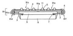
第5の実施形態は、両側に外部接続フィルム部を有するパッケージフィルムを用い、これらの外部接続フィルム部をそれぞれ折り曲げることを特徴とするものである。図9は本発明の第5の実施形態の半導体装置の構造および製造工程を示す図である。図9において、(a)はこの半導体装置に用いられるパッケージフィルム91をインナーリード形成面から見た正面図であり、(b)は(a)のA−A’間断面を含む第5の実施形態の半導体装置の断面構造図である。尚、図9において、図1ないし図8に示したものと同じものには同じ符号を付してある。
【0057】
まず、上記第1の実施形態と同様に手順により、図9(a)に示すパッケージフィルム91を作成する。すなわち、デバイスホール12と2つの折曲ホール13aおよび13bとが形成されたベース樹脂2にインナーリード3をパターニング形成し、さらにこの上に絶縁樹脂4をパターニング形成することにより外部電極パッド5を形成する。尚、ダミーインナーリードは必要ない。また、折曲部91d、91f(折曲ホール13a、13bの形成部)におけるインナーリード3の強度劣化を防止するために弾性樹脂6をコーティングすることが望ましい。以上により、パッケージフィルム91が作成される。
【0058】
次に、図9(b)に示すように、パッケージフィルム91のデバイス実装フィルム部91bのインナーリード形成面91A(第1面)側をLSΙチップ8の表面に対面させて、デバイス実装フィルム部91bにLSΙチップ8を実装する。すなわち、パッケージフィルム91のデバイス実装フィルム部91bにおいて、バンプ7が形成されたLSΙチップ8のチップ電極パッド8aに、熱圧着法によりインナーリード3を一括ボンディングし、デバイス実装フィルム部91bとLSΙチップ8の表面とにより形成される空間に封止樹脂9を流し込み、デバイス実装フィルム部91bに対してLSΙチップ8を固定実装する。次に、外部接続フィルム部91cおよび91eを、折曲部91dおよび91fにおいて、それぞれデバイス実装フィルム部91bのベース樹脂面1B(第2面)側に180゜折り曲げ、接着剤10a、10bによって封止樹脂9表面に固定する。最後に、外部電極パッド5に半田ボール11を搭載する。
【0059】
このように第5の実施形態によれば、デバイス実装フィルム部91bの両側に外部接続フィルム部91c、91eを設けたことにより、チップ電極パッドから外部電極パッドまでの配線(インナーリード)長を上記第1の実施形態よりも短くすることができ、より効率的な配線の引き回しが可能となるので、LSIチップの動作を高速化することができる。
【0060】
尚、上記第2の実施形態のように、パッケージフィルムのベース樹脂面側に外部電極パッドを形成しても良い。この場合は、デバイス実装フィルム部のベース樹脂面側をLSIチップ8の表面に対面させて、LSIチップ8を固定実装する。また、外部電極パッド5に半田ボール11を搭載しない構造としても良い。
【0061】
第5の参考例
第5の参考例は、パッケージフィルムの両側に形成された外部接続フィルム部を折り曲げてから封止樹脂を流し込み、パッケージフィルムにLSIチップを実装することを特徴とするものである。図10は第5の参考例の半導体装置を示す断面構造図である。尚、図10において、図1ないし図9に示したものと同じものには同じ符号を付してある。
【0062】
まず、上記第5の実施形態のパッケージフィルム91(図9(a)参照)を用い、このパッケージフィルム91のインナーリード形成面91A(第1面)をLSΙチップ8側にして、パッケージフィルム91のデバイス実装フィルム部91bにおいて、バンプ7が形成されたLSΙチップ8のチップ電極パッド8aに、熱圧着法によりインナーリード3およびダミーインナーリード3aを一括ボンディングする。次に、外部接続フィルム部91cおよび91eを、折曲部91dおよび91fにてそれぞれベース樹脂面1B側に180゜折り曲げる。
【0063】
次に、折曲げられた外部接続フィルム部91cと91eのすき間91gから封止樹脂9を注入し、この封止樹脂9により、LSIチップ8をデバイス実装フィルム部91bに固定実装するとともに、折り曲げられた外部接続フィルム部91cと91eをデバイス実装フィルム部91bに対して固定する。そして最後に、外部電極パッド5に半田ボール11を搭載する。
【0064】
このように第5の参考例によれば、外部接続フィルム部91cと91eを折り曲げ、これら外部接続フィルム部のすき間91gから封止樹脂9を注入して、LSIチップ8を固定実装するとともに、外部接続フィルム部91cおよび91eを固定することにより、外部接続フィルム部を固定するための接着剤、および外部接続フィルム部を接着剤で固定する工程が不要となるので、より低コスト化を図ることができる。
【0065】
尚、上記第2の実施形態のように、パッケージフィルムのベース樹脂面側に外部電極パッドを形成しても良い。また、外部電極パッド5に半田ボール11を搭載しない構造としても良い。
【0066】
第6の実施形態
第6の実施形態は、両側に外部接続フィルム部を有するパッケージフィルムに形成されたインナーリードを、バンプを形成しないでLSIチップの電極パッドに直接ボンディングすることを特徴とするものである。図11は本発明の第6の実施形態の半導体装置を示す断面構造図である。尚、図11において、図1ないし図10に示したものと同じものには同じ符号を付してある。
【0067】
まず、パッケージフィルム111を作成する。このパッケージフィルム111は、上記第5の実施形態のパッケージフィルム91(図9(a)参照)において、インナーリード3ではなく、上記第3の実施形態で用いた銅箔に金メッキを施したインナーリード31をパターニング形成し、このインナーリード31の硬度を下げるために、上記第3の実施形態と同様に、150℃、30分程度のアニール処理を施したものである。インナーリード31は、LSIチップ8のチップ電極パッド8aにバンプを介さずに熱圧着法により直接一括ボンディングされる。尚、これ以降以外の製造工程は、上記第5の実施形態と同じである。
【0068】
このように第6の実施形態によれば、LSIチップの電極パッドにバンプを形成する工程が不要となるので、上記第5の実施形態よりもさらに製造コストを削減でき、低価格化を図ることができる。
【0069】
尚、この第6の実施形態は、上記第5の参考例に対しても適用可能であることは言うまでもない。また、外部電極パッド5に半田ボール11を搭載しない構造としても良い。
【0070】
第6の参考例
第6の参考例は、パッケージフィルムの両側に形成された2つの外部接続フィルム部を折り曲げた構造の半導体装置に、LSIチップの側面および裏面を保護するための保護枠を設けたことを特徴とするものである。図12は第6の参考例の半導体装置を示す断面構造図である。尚、図12において、図1ないし図11に示したものと同じものには同じ符号を付してある。
【0071】
図12に示す半導体装置は、上記第5の実施形態の半導体装置に、図12(a)に示す箱型の保護枠41、あるいは図12(b)に示す底部がない保護枠42を取り付けたものである。これらの保護枠41および42は、上記第1の参考例で用いたものと同じであり、パッケージフィルム91のデバイス実装フィルム部91bに接着剤10cを用いて固定される。
【0072】
このように第6の参考例によれば、2つの外部接続フィルム部を折り曲げた構造の半導体装置に、保護枠41または42を取り付けることにより、LSIチップ8の側面および裏面を保護することができるので、ハンドリング時にLSIチップ8の側面およびチップ裏面の欠けが発生しなくなり、実装時の歩留まり向上が期待できる。
【0073】
尚、この第6の参考例は、上記第5の参考例または上記第6の実施形態に対しても適用可能であることは言うまでもない。また外部電極パッド5に半田ボール11を搭載しない構造としても良い。
【0074】
第7の参考例
第7の参考例は、パッケージフィルムの両側に形成され、LSIチップのパッケージフィルムへの実装の際に、それぞれ折り曲げられる外部接続フィルム部の平坦性を向上させるための板を設けたことを特徴とするものである。図13は第7の参考例の半導体装置の断面構造図である。尚、図13において、図1ないし図12に示したものと同じものには同じ符号を付してある。
【0075】
図13に示す半導体装置は、上記第5の実施形態の半導体装置において、パッケージフィルム91のデバイス実装フィルム部91bと外部接続フィルム部91cおよび91eの間に、上記第2の参考例で用いた絶縁材料または金属等の導電性材料からなる平板51を取り付けたものである。この平板51は、接着剤10a、10b、10cを用いてデバイス実装フィルム部91bの封止樹脂9表面と外部接続フィルム部91cおよび91eとの間に固定される。
【0076】
このように第7の参考例によれば、デバイス実装フィルム部91bと外部接続フィルム部91cおよび91eとの間に平板51を取り付けることにより、外部接続フィルム部91cおよび91eの平坦性すなわち半田ボール11の平坦性を向上させることができるので、マザーボードへの実装性を向上させることができる。また平板として金属板等を用いた場合には、半導体装置の熱放散性を向上させることができる。
【0077】
尚、この第7の参考例は、上記第6の実施形態または第6の参考例に対しても適用可能であることは言うまでもない。また、外部電極パッド5に半田ボール11を搭載しない構造としても良い。また、平板を用いずに、上記第4の実施形態のようなコの字板を用いても良い。
【0078】
さらに、導電性の平板またはコの字板を用い、上記第3の参考例のように、パッケージフィルム91に基準電源インナーリードを形成するとともに、外部接続フィルム部91cおよび91eにそれぞれスルーホールを設け、このスルーホールを介して基準電源インナーリードと導電性の平板またはコの字板とを電気的に接続することにより、外部接続フィルム部を2層両面導電層構造としても良い。これにより、クロストークノイズを低減させることができるので、LSIチップの動作をさらに高速化することができる。
【0079】
第7の実施形態
第7の実施形態は、パッケージフィルムの両側に形成された外部接続フィルム部を、それぞれLSIチップの裏面に折り曲げて固定することを特徴とするものである。図14は本発明の第7の実施形態の半導体装置を示す断面構造図である。尚、図14において、図1ないし図13に示したものと同じものには同じ符号を付してある。
【0080】
図14において、まず、上記第5の実施形態におけるパッケージフィルム91(図9(a)参照)を用い、パッケージフィルム91のデバイス実装フィルム部91bのベース樹脂面91B(第2面)側をLSΙチップ8の表面に対面させて、デバイス実装フィルム部91bにLSΙチップ8を実装する。すなわち、パッケージフィルム91のデバイス実装フィルム部91bにおいて、バンプ7が形成されたLSΙチップ8のチップ電極パッド8aに、熱圧着法によりインナーリード3を一括ボンディングし、デバイス実装フィルム部1bとLSΙチップ8の表面により形成される空間に封止樹脂9を流し込み、デバイス実装フィルム部1bに対してLSΙチップ8を固定実装する。
【0081】
次に、外部接続フィルム部91cおよび91eを、折曲部91dおよび91fにてそれぞれLSIチップ8の裏面8b側に180゜折り曲げ、接着剤10a、10bによってチップ裏面8bに固定する。最後に、外部電極パッド5に半田ボール11を搭載する。
【0082】
このように第7の実施形態によれば、外部接続フィルム部91c、91eをLSIチップ8の裏面8bに折り曲げて固定することにより、保護枠等を用いずに、LSIチップ8の裏面8bおよび側面を保護することができる。また、平板を用いずに外部接続フィルム部91c、91eの平坦化を図ることができる。
【0083】
尚、上記第2の実施形態のように、パッケージフィルムのベース樹脂面側に外部電極パッドを形成しても良い。この場合は外部接続フィルム部のインナーリード形成面がLSIチップ8の裏面に接着される。また、上記第3の実施形態および第6の実施形態のように、バンプを用いずにインナーリードをチップ電極パッド8aに直接ボンディングしても良い。また、外部電極パッド5に半田ボール11を搭載しない構造としても良い。
【0084】
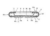
第8の実施形態
第8の実施形態は、4つの外部接続フィルム部を四方に有するパッケージフィルムを用い、これらの外部接続フィルム部をそれぞれ折り曲げることを特徴とするものである。図15は本発明の第8の実施形態の半導体装置の構造および製造工程を示す図である。図15において、(a)はこの半導体装置に用いられるパッケージフィルム151をインナーリード形成面151Aから見た正面図であり、(b)は(a)のA−A’間断面を含む第8の実施形態の半導体装置の断面構造図である。尚、図15において、図1ないし図14に示したものと同じものには同じ符号を付してある。
【0085】
まず、上記第1の実施形態と同様な手順により、図15(a)に示すパッケージフィルム151を作成する。すなわち、デバイスホール12が形成され、さらにこのデバイスホール12を取り囲んで折曲ホール13cが枠状に形成されたベース樹脂2に、インナーリード3をパターニング形成し、さらにこの上に絶縁樹脂4をパターニング形成することにより外部電極パッド5を形成する。尚、ダミーインナーリードは必要ない。また、折曲部151d、151f、151j、151k(四角形の枠状に形成された折曲ホール13cの4辺にそれぞれ対応する部分)におけるインナーリード3の強度劣化を防止するために弾性樹脂6をコーティングすることが望ましい。以上により、パッケージフィルム151が作成される。
【0086】
次に、図15(b)に示すように、パッケージフィルム151のデバイス実装フィルム部151bのインナーリード形成面151A(第1面)をLSIチップ8の表面に対面させて、デバイス実装フィルム部151bにLSIチップ8を実装する。すなわち、パッケージフィルム151のデバイス実装フィルム部151bにおいて、バンプ7が形成されたLSIチップ8のチップ電極パッド8aに、熱圧着法によりインナーリード3を一括ボンディングし、デバイス実装フィルム部151bとLSΙチップ8の表面とにより形成される空間に封止樹脂9を流し込み、デバイス実装フィルム部151bに対してLSΙチップ8を固定実装する。次に、外部接続フィルム部151c、151e、151h、151iを、折曲部151d、151f、151j、151kにおいて、それぞれデバイス実装フィルム部151bのベース樹脂面151B(第2面)側に180゜折り曲げ、接着剤10a、10bによって封止樹脂9表面に固定する。最後に、外部電極パッド5に半田ボール11を搭載する。
【0087】
このように第8の実施形態によれば、デバイス実装フィルム部151bの四方にそれぞれ外部接続フィルム部を設けたことにより、チップ電極パッドから外部電極パッドまでの配線(インナーリード)長を上記第5の実施形態よりもさらに短くすることができ、より効率的な配線の引き回しが可能となるので、LSIチップの動作をさらに高速化することができる。
【0088】
尚、上記第5の参考例のように、4つの外部接続フィルム部を折り曲げ、そのすき間から封止樹脂9を流し込こむようにしても良い。また、上記第3の実施形態および第6の実施形態のように、バンプを用いずにインナーリードをチップ電極パッド8aに直接ボンディングしても良い。また、外部電極パッド5に半田ボール11を搭載しない構造としても良い。
【0089】
第8の参考例
第8の参考例は、4つの外部接続フィルム部を折り曲げた構造の半導体装置に、LSIチップの側面および裏面を保護するための保護枠を設けたこと、あるいは折り曲げらる外部接続フィルム部の平坦性を向上させるための平板を設けたことを特徴とするものである。図16は第8の参考例の半導体装置を示す断面構造図である。尚、図16において、図1ないし図15に示したものと同じものには同じ符号を付してある。
【0090】
図16に示す半導体装置は、上記第8の実施形態の半導体装置に、図16(a)に示す箱型の保護枠41、あるいは図16(b)に示すように底部がない保護枠42を取り付けたものである。これらの保護枠41および42は、上記第1の参考例で用いたものと同じであり、パッケージフィルム151のデバイス実装フィルム部151bに接着剤10cを用いて固定される。
【0091】
このように第8の参考例によれば、4つの外部接続フィルム部を折り曲げた構造の半導体装置に保護枠41または42を取り付けることにより、LSIチップ8の側面および裏面を保護することができるので、ハンドリング時にLSIチップ8の側面およびチップ裏面の欠けが発生しなくなり、実装時の歩留まり向上が期待できる。
【0092】
尚、保護枠41または42ではなく、上記第2の参考例のような平板を4つの外部接続フィルム部と封止樹脂9表面の間に設けた構成、あるいは保護枠41または42と上記の平板とをともに設けた構成としても良い。さらに、導電性平板を用い、上記第3の参考例のように、パッケージフィルム151に基準電源インナーリードを形成するとともに、4つの外部接続フィルム部にそれぞれスルーホールを設け、このスルーホールを介して基準電源インナーリードと導電性平板とを電気的に接続することにより、外部接続フィルム部を2層両面導電層構造としても良い。また、外部電極パッド5に半田ボール11を搭載しない構造としても良い。
【0093】
第9の実施形態
第9の実施形態は、パッケージフィルムの四方に形成された外部接続フィルム部を、それぞれLSIチップの裏面に折り曲げて固定することを特徴とするものである。図17は本発明の第9の実施形態の半導体装置を示す断面構造図である。尚、図17において、図1ないし図16に示したものと同じものには同じ符号を付してある。
【0094】
図17において、まず、上記第8の実施形態におけるパッケージフィルム151(図15(a)参照)を用い、パッケージフィルム151のデバイス実装フィルム部151bのベース樹脂面151B(第2面)側をLSΙチップ8の表面に対面させて、上記第7の実施形態と同様の手順で、デバイス実装フィルム部151bにLSΙチップ8を固定実装する。次に、外部接続フィルム部151c、151hを含む4つの外部接続フィルムを、折曲部151dおよび151fを含む4つの折曲部において、それぞれLSIチップ8の裏面8b側に180゜折り曲げ、接着剤10a、10bによってチップ裏面8bに固定する。最後に、外部電極パッド5に半田ボール11を搭載する。
【0095】
このように第9の実施形態によれば、4つの外部接続フィルム部をLSIチップ8の裏面8bに折り曲げて固定することにより、保護枠等を用いずに、LSIチップ8の裏面8bおよび側面を保護することができる。また、平板を用いずに外部接続フィルム部の平坦化を図ることができる。
【0096】
尚、上記第2の実施形態のように、パッケージフィルムのベース樹脂面側に外部電極パッドを形成しても良い。この場合は外部接続フィルム部のインナーリード形成面がLSIチップ8の裏面に接着される。また、上記第3の実施形態のように、バンプを用いずにインナーリードをチップ電極パッド8aに直接ボンディングしても良い。また、外部電極パッド5に半田ボール11を搭載しない構造としても良い。
【0097】
第10の実施形態
第10の実施形態は、チップ電極パッドがチップ表面の中心線付近に形成されたLSIチップを用いることを特徴とするものである。図18は本発明の第10の実施形態の半導体装置の構造および製造工程を示す図である。図18において、(a)はこの半導体装置に用いるパッケージフィルム181の外部接続面181Aから見た上面図、(b)は(a)におけるA−A’間の断面図、(c)はこの半導体装置の断面構造図である。尚、図18において、図1ないし図17に示したものと同じものには同じ符号を付してある。
【0098】
図18(a)および(b)に示すように、チップ電極パッド182aがチップ中心線に沿った領域に形成されたLSIチップ182に対して、上記第2の実施形態と同様の手順で、LSI182のチップ電極パッド形成領域に対応して、中心線Fに沿った領域にデバイスホール183を有するパッケージフィルム181を作成する。このとき折曲ホールは形成せず、またパッケージフィルム181の大きさは、略LSIチップと同じとする。
【0099】
次に図18(c)に示すように、上記第2の実施形態と同様の手順で、LSIチップ182のチップ電極パッド182aにインナーリード3をボンディングしてパッケージフィルム181にLSIチップ182を実装し(ただし、パッケージフィルムを折り曲げる工程はない)、外部電極パッド22に半田ボール11を搭載する。
【0100】
このように第10の実施形態によれば、チップ電極パッド182aがチップ中心線に沿って形成されたLSIチップ182を、チップ電極パッド形成領域に対応した位置にデバイスホール183を有し、LSIチップ182と略同じ大きさのパッケージフィルム181に実装することにより、特殊な弾性接着剤や熱膨張率がLSIチップと異なる基板を用いないため、半導体装置の信頼性を向上させることができる。また、加工工数(パッケージフィルムの折り曲げ工数等)および材料費を削減できるので、さらに半導体装置の低価格化を図ることができる。また、上記第1の実施形態と比較して小型化、軽量化が可能である。
【0101】
尚、上記第3の実施形態のように、インナーリードをチップ電極パッドに直接ボンディングするようにしても良い。また、外部電極パッド22に半田ボール11を搭載しない構造としても良い。
【0102】
第11の実施形態
第11の実施形態は、チップ電極パッドがチップ表面の中央部に形成されたLSIチップを用いることを特徴とするものである。図19は本発明の第11の実施形態の半導体装置の構造および製造工程を示す図である。図19において、(a)はこの半導体装置に用いるパッケージフィルム191の外部接続面191Aから見た上面図であり、(b)は(a)におけるA−A’間の断面を含む第11の実施形態の半導体装置の断面構造図である。尚、図19において、図1ないし図18に示したものと同じものには同じ符号を付してある。
【0103】
まず、図19(a)に示すように、チップ電極パッド192aがチップ中心付近に形成されたLSIチップ192に対し、上記第1の実施形態と同様の手順で、LSIチップ192のチップ電極パッド形成領域に対応して、中央部にデバイスホール193を有するパッケージフィルム191を作成する。パッケージフィルム191の大きさはLSIチップ192と略同じであり、またデバイスホール193は、LSIチップ192のチップ電極パッド形成領域に対応した位置および形状に形成されている。パッケージフィルム191においては、インナーリード形成面側に外部電極パッド5が形成されており、インナーリード形成面が外部接続面191Aとなる。またパッケージフィルム191の樹脂面は、LSIチップ191が実装される側であるデバイス実装面191Bとなる。
【0104】
次に、図19(b)に示すように、上記第1の実施形態と同様の手順で、LSIチップ192のチップ電極パッド192aにインナーリード3を一括ボンディングして、パッケージフィルム191のデバイス実装面191B側にLSIチップ192を実装し(ただしパッケージフィルムを折り曲げる工程はない)、外部電極パッド5に半田ボール11を搭載する。
【0105】
このように第11の実施形態によれば、チップ電極パッド192aがチップ中央部に形成されたLSIチップ192を、チップ電極パッド形成領域に対応した位置にデバイスホール193を有し、LSIチップ192と略同じ大きさのパッケージフィルム191に実装することにより、特殊な弾性接着剤や熱膨張率がLSIチップと異なる基板を用いないため、半導体装置の信頼性を向上させることができる。また、加工工数(パッケージフィルムの折り曲げ工数等)および材料費を削減できるので、さらに半導体装置の低価格化を図ることができる。また、上記第1の実施形態と比較して小型化、軽量化が可能である。
【0106】
尚、上記第3の実施形態のように、インナーリードをチップ電極パッドに直接ボンディングするようにしても良い。また、外部電極パッド5に半田ボール11を搭載しない構造としても良い。
【0107】
第12の実施形態
第12の実施形態は、上記第10の実施形態または第11の実施形態において、デバイス実装面に絶縁樹脂突起を有するパッケージフィルムを用いることを特徴とするものである。図20は本発明の第12の実施形態の半導体装置を示す断面構造図である。尚、図20において、図1ないし図19に示したものと同じものには同じ符号を付してある。
【0108】
図20に示す半導体装置は、上記第10の実施形態の半導体装置において、パッケージフィルム181ではなく、デバイス実装面に絶縁樹脂突起を有するパッケージフィルム201を用いたものである。パッケージフィルム201のデバイス実装面201B側には、絶縁樹脂突起202が設けられている。この絶縁樹脂突起202は、インナーリード3がパターニングされたベース樹脂2に絶縁樹脂をコーティングし、この絶縁樹脂にフォトリソエッチングを施すことにより、容易に形成することが可能である。
【0109】
次に、上記第10の実施形態と同じ手順で、LSIチップ182のチップ電極パッド182aにインナーリード3をボンディングし、封止樹脂9をLSIチップ182の表面とパッケージフィルム201との空間に流し込み、LSIチップ182を固定実装する。このとき、絶縁樹脂突起202の頂部202aがLSIチップ182の表面に接触するようにパッケージフィルム201とLSIチップ182を配置して、封止樹脂9を流し込む。また、絶縁樹脂突起202は、封止樹脂9を流れ易くさせ、パッケージフィルム201の平坦度を向上させる機能を有する。
【0110】
このように第12の実施形態によれば、パッケージフィルム201のデバイス実装面201Bに絶縁樹脂突起202を設けたことにより、封止樹脂9を流れ易くさせることができ、またパッケージフィルム201の平担度を向上することができるので、パッケージの品質を向上させることができる。
【0111】
尚、第12の実施形態は、上記第11の実施形態にも適用可能であることは言うまでもない。また、外部電極パッド5に半田ボール11を搭載しない構造としても良い。
【0112】
第9の参考例
第9の参考例は、中心部あるいは中心線に沿った領域にデバイスホールを設けたパッケージフィルムを用いた半導体装置に、LSIチップの側面および裏面を保護するための保護枠を設けたことを特徴とするものである。図21は第9の参考例の半導体装置を示す断面構造図である。尚、図21において、図1ないし図20に示したものと同じものには同じ符号を付してある。
【0113】
図21に示す半導体装置は、上記第11の実施形態の半導体装置に、図21(a)に示す箱型の保護枠211、あるいは図21(b)に示す底部がない保護枠212を取り付けたものである。これらの保護枠211および212は、パッケージフィルム191のデバイス実装面191Bに接着剤10を用いて固定される。
【0114】
このように第9の参考例によれば、保護枠211または212を取り付けることにより、LSIチップ192の側面および裏面を保護することができるので、ハンドリング時にLSIチップ192の側面およびチップ裏面の欠けが発生しなくなり、実装時の歩留まり向上が期待できる。
【0115】
尚、第9の参考例は、上記第10の実施形態または第12の実施形態にも適用可能であることは言うまでもない。また、外部電極パッド5に半田ボール11を搭載しない構造としても良い。
【0116】
第13の実施形態
図22は本発明の第13の実施形態の半導体装置を示す断面構造図である。尚、図22において、図1ないし図21に示したものと同じものには同じ符号を付してある。
【0117】
図22に示す半導体装置は、パッケージフィルム221と、上記第11の実施形態で用いたLSIチップ192からなる。パッケージフィルム221は、デバイス実装フィルム部221bの四方に、上記第8の実施形態のパッケージフィルム151(図15(a)参照)のように、折曲部221d、221jを含む4つの折り曲げ部を介して、外部接続フィルム部221c、221hを含む4つの外部接続フィルム部を有する。
【0118】
まず、パッケージフィルム221を作成する。すなわち、LSIチップ192のチップ電極パッド形成領域に対応して、中心部にデバイスホール193が形成され、さらにこのデバイスホール193を取り囲んで折曲ホールが枠状に形成されたベース樹脂2に、上記第1の実施形態と同様の手順で、インナーリード3をパターニング形成し、さらにこの上に絶縁樹脂4をパターニング形成することにより外部電極パッド5を形成する。デバイス実装フィルム部221bのインナーリード形成面(第1面)側にも外部電極パッド5が形成されている。デバイス実装フィルム部221bは、上記第11の実施形態のパッケージフィルム191(図19(a)参照)と同じ構造であり、パッケージフィルム221は、上記第11の実施形態のパッケージフィルム191に4つの外部接続フィルム部を設けた構造である(ただし、デバイス実装フィルム部221bにおけるバイスホール193は、パッケージフィルム191におけるバイスホール193を45゜回転させたものとして図示してある)。尚、4つの折曲部におけるインナーリード3の強度劣化を防止するために弾性樹脂6をコーティングすることが望ましい。以上により、パッケージフィルム221が作成される。
【0119】
次に、デバイス実装フィルム部221bのベース樹脂面(第2面)をLSIチップ192の表面に対面させて、上記第11の実施形態と同様にして、デバイス実装フィルム部221bにLSIチップ192を実装する。すなわち、バンプ7が形成されたLSIチップ192のチップ電極パッド192aに、熱圧着法によりインナーリード3を一括ボンディングし、デバイス実装フィルム部221bとLSIチップ192の表面とにより形成される空間に封止樹脂9を流し込み、デバイス実装フィルム部221bにLSIチップ192を固定実装する。
【0120】
次に、4つの外部接続フィルム部(外部接続フィルム部221c、221h等)を、4つの折曲部(折曲部221d、221j等)において、それぞれLSIチップ192の裏面192b側に180゜折り曲げ、接着剤10a、10b等によってチップ裏面192bに固定する。最後に、4つの外部接続フィルム部の外部電極パッド5にそれぞれ半田ボール11を搭載する。ここでは、デバイス実装フィルム部221bの外部電極パッド5には半田ボール11を搭載しない。
【0121】
図22に示す半導体装置は、次のようにして複数積層することができる。積層個数をN(Nは2以上の整数)とする。第1の半導体装置の外部接続フィルム部と、第2の半導体装置のデバイス実装フィルム部221bを対面させ、それぞれの外部電極パッド5が重なり合うように、2つの半導体装置を積層し、第1の半導体装置の外部電極パッド5に搭載されている半田ボール11を溶解させて、重なり合った外部電極どうしを電気的に接続する。また、これにより、第2の半導体装置は、第1の半導体装置上に積層固定される。同様にして第3〜第Nの半導体装置を積層する。半田ボール11の溶解は、N個の半導体装置を積み重ねてから一括して行うようにしても良い。ただし、上記のように、第1の半導体装置の外部接続フィルム部と、第2の半導体装置のデバイス実装フィルム部221bを対面させる場合には、デバイス実装フィルム部221bの外部電極パッド5の形成位置に対応するように、外部接続フィルム部の外部電極パッド5を形成しておく必要がある。尚、デバイス実装フィルム部221bどうし、あるいは外部接続フィルム部どうしを対面させて積層しても良い。もちろん、上記と同様の手順により、図22に示す半導体装置を、マザーボードに複数積層して実装することも可能である。
【0122】
このように第13の実施形態によれば、デバイス実装フィルム部221bにも外部電極パッド5を設け、外部接続フィルム部をLSIチップの裏面に固定することにより、配線長の短縮、LSIチップ裏面の保護、および外部接続フィルム部の平坦化を図ることができるとともに、マザーボードへの積層実装(立体実装)が可能となるので、マザーボードにおける実装スペースの省スペース化を図ることができる。
【0123】
尚、上記第5の実施形態のように、外部接続フィルム部をデバイス実装フィルム部221bの両側に2つ設けても良い。また、デバイス実装フィルム部のみに半田ボール11を搭載しても良い。また、外部接続フィルム部とデバイス実装フィルム部に、ともに半田ボール11を搭載する、あるいはともに半田ボール11を搭載しないようにしても良い。また、上記第3の実施形態のようにインナーリードをチップ電極パッドに直接ボンディングするようにしても良い。また、デバイス実装フィルム部221bの第2面に、上記第12の実施形態のように絶縁樹脂突起を設けても良い。
【0124】
第14の実施形態
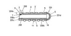
図23は本発明の第14の実施形態の半導体装置を示す断面構造図である。尚、図22において、図1ないし図21に示したものと同じものには同じ符号を付してある。
【0125】
図23に示す半導体装置は、パッケージフィルム231と、チップ表面の周辺部にチップ電極パッド232aが形成されたLSIチップ232からなる。パッケージフィルム231は、デバイス実装フィルム部231bと、外部接続フィルム部231cと、これらの間に位置する折曲部231dにより構成される。
【0126】
まず、パッケージフィルム221を作成する。すなわち、LSIチップ232のチップ電極パッド形成領域に対応して、周辺部にデバイスホール233が形成され、さらに折曲ホールが形成されたベース樹脂2に、上記第1の実施形態と同様の手順で、インナーリード3をパターニング形成し、さらにこの上に絶縁樹脂4をパターニング形成することにより外部電極パッド5を形成する。デバイス実装フィルム部231bのインナーリード形成面側にも外部電極パッド5が形成されている。尚、デバイスホール233は、「ホール」ではなく、周辺部に設けた切り欠きであるが、機能としては上記第10の実施形態のデバイスホール183等と同じであるので、「ホール」と称することとする。また、折曲部におけるインナーリード3の強度劣化を防止するために弾性樹脂6をコーティングすることが望ましい。以上により、パッケージフィルム231が作成される。
【0127】
次に、デバイス実装フィルム部231bのベース樹脂面をLSIチップ232の表面に対面させて、上記第11の実施形態と同様にして、デバイス実装フィルム部231bにLSIチップ232を実装する。すなわち、バンプ7が形成されたLSIチップ232のチップ電極パッド232aに、熱圧着法によりインナーリード3を一括ボンディングし、デバイス実装フィルム部231bとLSIチップ232の表面とにより形成される空間に封止樹脂9を流し込み、デバイス実装フィルム部231bにLSIチップ232を固定実装する。
【0128】
次に、外部接続フィルム部231cを折曲部231dにおいてLSIチップ232の裏面232b側に180゜折り曲げ、接着剤10によってチップ裏面192bに固定する。
最後に、外部接続フィルム部232cの外部電極パッド5に半田ボール11を搭載する。
ここでは、デバイス実装フィルム部231bの外部電極パッド5には半田ボール11を搭載しない。
【0129】
図23に示す半導体装置も、上記第13の実施形態と同様にして、複数積層することができる。従って、図22に示す半導体装置を、マザーボードに複数積層して実装することも可能である。
【0130】
このように第14の実施形態によれば、デバイス実装フィルム部231bにも外部電極パッド5を設け、外部接続フィルム部231cをLSIチップの裏面に固定することにより、配線長の短縮、LSIチップ裏面の保護、および外部接続フィルム部の平坦化を図ることができるとともに、マザーボードへの積層実装(立体実装)が可能となるので、マザーボードにおける実装スペースの省スペース化を図ることができる。さらに、外部接続フィルム部が1つなので、上記第13の実施形態と比較して、外部電極パッド5の位置精度を向上させることができる。
【0131】
尚、デバイス実装フィルム部231bのみに半田ボール11を搭載しても良い。また、外部接続フィルム部231cとデバイス実装フィルム部231bに、ともに半田ボール11を搭載する、あるいはともに半田ボール11を搭載しないようにしても良い。また、上記第3の実施形態のようにインナーリードをチップ電極パッドに直接ボンディングするようにしても良い。また、外部接続フィルム部を複数設けても良い。また、デバイス実装フィルム部221bの第2面に、上記第12の実施形態のように絶縁樹脂突起を設けても良い。また、上記第10の実施形態または第11の実施形態のように、外部接続フィルム部および折曲部がない構造としても良い。
【0132】
【発明の効果】
以上説明したように、本発明の請求項1記載の半導体装置によれば、インナーリードを半導体チップの電極パッドにボンディングして半導体チップをデバイス実装フィルム部に実装し、外部接続フィルム部を折曲部にて180゜折曲げて固定することにより、特殊な弾性接着剤や半導体チップと熱膨張率のことなる基板を用いないため、半導体装置の信頼性を向上させることができ、かつ専用の金型を必要としないため、製造コストを低減することができ、従って半導体装置の低価格化を図ることができるという効果がある。
【0133】
また、請求項1記載の半導体装置によれば、コの字板の底板の内面に半導体チップを取り付け、天板の外面に外部接続フィルム部を取り付けることにより、外部接続フィルム部の平坦性を向上させることができるとともに、半導体チップを保護することができるという効果がある。またコの字板として金属板等を用いた場合には、パッケージの熱放散性をさらに向上させることができるという効果がある。
【0134】
請求項4記載の半導体装置および請求項18記載の製造方法によれば、半導体装置の低価格化および信頼性の向上を図ることができるので、マザーボードへの実装性を向上させることができるとともに、外部接続フィルム部を半導体チップの裏面に固定することにより、半導体チップの裏面および側面を保護することができ、外部接続フィルム部の平坦化を図ることができるという効果がある。
【0135】
請求項2、3記載の半導体装置および請求項16、17記載の製造方法によれば、半導体チップの電極パッド形成領域に対応した位置にデバイスホールを有するパッケージフィルムに実装することにより、特殊な弾性接着剤や熱膨張率が半導体チップと異なる基板を用いないため、信頼性を向上させることができ、また加工工数および材料費を削減できるので、さらにパッケージの低価格化を図ることができるという効果がある。
【0136】
また、請求項4記載の半導体装置および請求項18記載の製造方法によれば、半導体装置の低価格化および信頼性の向上を図ることができるとともに、デバイス実装フィルム部にも外部電極パッドを設け、外部接続フィルム部を半導体チップの裏面に固定することにより、配線長の短縮、半導体チップ裏面の保護、および外部接続フィルム部の平坦化を図ることができるという効果がある。また、マザーボードにおける実装スペースの省スペース化等を目的とした半導体装置の積層が可能となるという効果がある。
【0137】
請求項2、3、8記載の半導体装置および請求項16、17、19記載の製造方法によれば、絶縁樹脂突起を設けたことにより、封止樹脂を流れ易くさせることができ、またパッケージフィルムの平担度を向上することができるので、半導体装置の品質を向上させることができるという効果がある。
【0138】
請求項9記載の半導体装置および請求項22記載の製造方法によれば、外部接続フィルム部を複数設けることにより、チップ電極パッドから外部電極パッドまでの配線(インナーリード)長を短くすることができ、より効率的な配線の引き回しが可能となるので、半導体チップの動作を高速化することができるという効果がある。
【0139】
請求項12記載の半導体装置によれば、パッケージフィルムの折曲部において、インナーリードを弾性樹脂でコーティングすることにより、折曲部でのインナーリードの強度劣化あるいは断線を防止することができるという効果がある。
【0140】
請求項13記載の半導体装置および請求項29記載の製造方法によれば、半導体チップの電極パッドにバンプを形成する工程が不要となるので、製造コストを削減でき、パッケージの低価格化を図ることができる。
【0141】
請求項28記載の製造方法によれば、インナーリードを半導体チップの電極パッドに一括ボンディングすることにより、加工工数が削減され、製造コストを低減することができるので、パッケージの低価格化を図ることができる。
【0142】
請求項30記載の実装方法によれば、マザーボード側に半田ボールを供給することにより、複数のパッケージを同時に実装することが可能となるので、半導体装置のマザーボードに対する実装工数を削減することができるという効果があり、また半導体装置の製造工程においては、外部電極パッドに半田ボールを搭載する工程が不要となるので、加工工数を削減でき、パッケージの低価格化をさらに図ることができるという効果がある。
【0143】
請求項31記載の実装方法によれば、半導体装置を積層実装することにより、マザーボードの省スペース化を図ることができるという効果がある。
【図面の簡単な説明】
【図1】 本発明の第1の実施形態の半導体装置の構造および製造工程を示す図である。
【図2】 本発明の第2の実施形態の半導体装置の構造および製造工程を示す図である。
【図3】 本発明の第3の実施形態の半導体装置の断面構造図である。
【図4】第1の参考例の半導体装置の断面構造図である。
【図5】第2の参考例の半導体装置の断面構造図である。
【図6】 本発明の第4の実施形態の半導体装置の断面構造図である。
【図7】第3の参考例の半導体装置の構造および製造工程を示す図である。
【図8】第4の参考例の半導体装置の構造および製造工程を示す図である。
【図9】 本発明の第5の実施形態の半導体装置の構造および製造工程を示す図である。
【図10】第5の参考例の半導体装置の断面構造図である。
【図11】 本発明の第6の実施形態の半導体装置の断面構造図である。
【図12】第6の参考例の半導体装置の断面構造図である。
【図13】第7の参考例の半導体装置の断面構造図である。
【図14】 本発明の第7の実施形態の半導体装置の断面構造図である。
【図15】 本発明の第8の実施形態の半導体装置の構造および製造工程を示す図である。
【図16】第8の参考例の半導体装置の断面構造図である。
【図17】 本発明の第9の実施形態の半導体装置の断面構造図である。
【図18】 本発明の第10の実施形態の半導体装置の構造および製造工程を示す図である。
【図19】 本発明の第11の実施形態の半導体装置の構造および製造工程を示す図である。
【図20】 本発明の第12の実施形態の半導体装置の断面構造図である。
【図21】第9の参考例の半導体装置の断面構造図である。
【図22】 本発明の第13の実施形態の半導体装置の断面構造図である。
【図23】 本発明の第14の実施形態の半導体装置の断面構造図である。
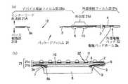
【図24】 従来のモールドタイプのパッケージを有する半導体装置の一部破断斜視図である。
【図25】 従来のフィルムタイプのパッケージを有する半導体装置の断面構造図である。
【図26】 従来のフリップチップボンディングタイプのパッケージを有する半導体装置の断面構造図である。
【符号の説明】
1,21,71,91,111,151,181,191,201,221,231 パッケージフィルム、 1A,21A,91A,151A インナーリード形成面、 1B,21B,91B,151B ベース樹脂面、 1b,21b,71b,91b,151b,221b デバイス実装フィルム部、 1c,21c,71c,91c,91e,151c,151e,151h,151i,221c,221h,231c 外部接続フィルム部、 1d,21d,91d,91f,151d,151f,151j,151k,221d,221f,231d 折曲部、 2 ベース樹脂、 2a,4a 電極パッドホール、 2b スルーホール、 3,31 インナーリード、 3b 基準電源インナーリード、 4 絶縁樹脂、 5,22 外部電極パッド、 6 弾性樹脂、 8,182,192,232 LSIチップ、 8a,182a,192a,232a チップ電極パッド、 8b チップ裏面 9 封止樹脂、 10,10a,10b,10c 接着剤、 11,11a 半田ボール、 12,183,193,233 デバイスホール、 31a 銅箔、 31b 金メッキ、 41,42 保護枠、 51 平板、 61 コの字板、 61a 底板、 61b 天板、 61c 湾曲部、 72 導電性平板、 91g すき間、 181A,191A,201A 外部接続面、 181B,191B,201B デバイス実装面、 202 絶縁樹脂突起、 202a 頂部。[0001]
BACKGROUND OF THE INVENTION
The present invention relates to a semiconductor device having a package that is substantially the same size as a semiconductor chip, and particularly suitable for a multi-output semiconductor chip, and a manufacturing method and a mounting method thereof.
[0002]
[Prior art]
Conventionally, packages of approximately the same size as this type of semiconductor chip are referred to as a chip size package, μ-BGA, chip scale package, CSP, and the like, and various types have been developed. FIG. 24 is a partially broken perspective view of a semiconductor device having a conventional mold type package. In this semiconductor device,
[0003]
FIG. 25 is a cross-sectional view of a semiconductor device having a conventional film (film carrier tape) type package. In this semiconductor device, the surface of the
[0004]
FIG. 26 is a cross-sectional view of a semiconductor device having a conventional flip chip bonding type package. In this semiconductor device,
[0005]
[Problems to be solved by the invention]
However, the semiconductor device shown in FIG. 24 requires a dedicated transfer mold, which has been an obstacle to cost reduction.
[0006]
In the semiconductor device shown in FIG. 25, since a special elastic adhesive is used between the LSI chip and the tape, the LSI chip surface may be contaminated or damaged, and the reliability may be deteriorated. In addition, when connecting the LSΙchip and the inner lead, single point bonding is used in which the leads are bonded one by one. In a multi-output package, the bonding time becomes long, which is an obstacle to cost reduction.
[0007]
Further, in the semiconductor device shown in FIG. 26, in a multi-output package, the substrate is multi-layered and expensive, and in a large LSI chip, there is a problem in reliability due to a difference in thermal expansion between the substrate and the LSL chip. It was.
[0008]
The present invention eliminates such a conventional problem, and provides a low-cost and high-reliability semiconductor device suitable for using a multi-output LSI chip, and a method for manufacturing and mounting the same. Objective.
[0009]
[Means for Solving the Problems]
To achieve the above object, the present inventionClaim 1The semiconductor device includes a device mounting film portion on which a semiconductor chip is mounted, an external connection film portion that is disposed on the device mounting film portion and has external electrode pads formed thereon, an end portion of the device mounting film portion, and the A bent portion provided between an end portion of the external connection film portion and an inner lead for electrically connecting the electrode pad of the semiconductor chip and the external electrode pad via the bent portion; Package filmAnd a U-shaped plate composed of a bottom plate and a top plate, the device mounting film portion attached to the inner surface of the U-shaped plate, and the external connection film portion attached to the outer surface of the top plateIt is characterized by that.
[0010]
The semiconductor device according to claim 2A package film on which a semiconductor chip in which pad electrodes are arranged in a central portion of the chip or a region along the center line of the chip is mounted, and the package film corresponds to a pad electrode formation region of the semiconductor chip, A device hole formed in a central portion or a region along the center line, an external electrode pad formed in a region other than the device hole forming region, and the electrode pad of the semiconductor chip and the external electrode pad are connected. With inner leadsAnd an insulating resin protrusion on the mounting surface of the semiconductor chip.It is characterized by that.
[0011]
A semiconductor device according to claim 3A package film on which a semiconductor chip having a pad electrode disposed on the periphery of the chip is mounted, the package film corresponding to a pad electrode formation region of the semiconductor chip and a device hole formed on the periphery An external electrode pad formed in a region other than the device hole formation region, and an inner lead for connecting the pad electrode of the semiconductor chip and the external electrode.And having an insulating resin protrusion on the mounting surface of the semiconductor chip.The space between the package film and the surface of the semiconductor chip is fixed with a sealing resin.
[0012]
A semiconductor device according to claim 4The device mounting film portion on which the semiconductor chip is mounted so as to face the surface of the semiconductor chip on which the electrode pad is disposed in a predetermined region, and the external electrode pad is formed on the back surface of the semiconductor chip. A package film having an external connection film portion, a bent portion provided between an end portion of the device mounting film portion and an end portion of the external connection film portion, and an inner lead; and the device mounting film portion Has a device hole formed in a predetermined region corresponding to a pad electrode formation region of the semiconductor chip, and an external electrode pad formed in a region other than the device hole formation region, and the inner lead Electrically connecting the electrode pads of the semiconductor chip and the external electrode pads of the device mounting film portion, Via a bent portion, characterized in that electrically connecting the external connection film portion and the electrode pads of the semiconductor chip.
[0013]
The semiconductor device according to an eighth aspect is the semiconductor device according to the fourth aspect, wherein the package film has an insulating resin protrusion on a mounting surface of the semiconductor chip. The semiconductor device according to
[0014]
Next, a manufacturing method of a semiconductor device according to
[0015]
The manufacturing method according to claim 17 comprises:A semiconductor chip in which electrode pads are arranged in the peripheral portion of the chip, and a device hole is formed in the peripheral portion corresponding to the pad electrode forming region of the semiconductor chip, and an external connection surface in a region other than the device hole forming region An external electrode pad is formed on the side, and an inner lead is formed from the device hole to the external electrode, and the inner lead is bonded to the electrode pad of the semiconductor chip in the device hole forming region. And a step of pouring a sealing resin between the package film and the surface of the semiconductor chip to mount the semiconductor chip on the device mounting surface side of the package film.The semiconductor chip mounting step is to fix the semiconductor chip to the package film by bonding an inner lead and then pouring a sealing resin into the space between the package film and the semiconductor chip.It is characterized by that.
[0016]
The manufacturing method according to claim 18 comprises:A semiconductor chip in which electrode pads are arranged in a predetermined region; a device mounting film portion in which a device hole is formed in a predetermined region corresponding to the pad electrode formation region of the semiconductor chip; and an external connection film portion; The external mounting film portion on the first surface side and the device mounting on the first surface side have a planar shape divided into a bent portion located between the device mounting film portion and the external connection film portion In the device hole formation region, an external electrode pad is formed in a region other than the device hole formation region of the film portion, and an inner lead is formed so as to reach each external electrode pad from the device hole. The inner lead is bonded to an electrode pad on the surface of the semiconductor chip, and the device on the second surface side is bonded. The step of mounting the semiconductor chip on the mounting film portion, and the step of bending the external connection film portion 180 ° to the back side of the semiconductor chip at the bent portion and fixing to the back surface are sequentially performed. To do.
[0017]
The manufacturing method according to claim 19 is the manufacturing method according to claim 18, wherein the device mounting film portion has an insulating resin protrusion formed on the second surface side, and the mounting process of the semiconductor chip includes In addition, after bonding the inner lead, a sealing resin is poured into the space between the device mounting film portion and the semiconductor chip to fix the semiconductor chip to the second surface of the device mounting film portion. Features. The manufacturing method according to
[0018]
A manufacturing method according to a twenty-eighth aspect is characterized in that, in the manufacturing method according to the eighteenth aspect, the mounting step of the semiconductor chip is to collectively bond the inner lead to an electrode pad of the semiconductor chip. The manufacturing method according to claim 29 is characterized in that, in the manufacturing method according to claim 18, the inner lead is directly bonded to the pad electrode of the semiconductor chip.
[0019]
Next, the present inventionClaim 30The semiconductor device mounting method ofThe method according to claim 1.A semiconductor device mounting method for closely mounting a semiconductor device on a mother board, mounting solder balls on electrode pads of the mother board, placing the semiconductor device on the mother board, dissolving the solder balls, The electrode pad of the motherboard and the external electrode pad of the semiconductor device are electrically connected.
[0020]
A semiconductor device mounting method according to a thirty-first aspect is the fourth aspect.A semiconductor device mounting method in which a plurality of semiconductor devices are stacked and mounted on a motherboard, wherein the semiconductor device is formed on an electrode pad of the motherboard on either the external connection film portion or the device mounting film portion of the first semiconductor device. The external electrode pad is overlapped and further formed on either the external connection film portion or the device mounting film portion of the second semiconductor device on the external electrode pad formed on the other film portion of the first semiconductor device. External electrode pads are stacked, and the overlapped electrodes are electrically connected to each other.
[0021]
DETAILED DESCRIPTION OF THE INVENTION
First embodiment
FIG. 1 is a diagram showing the structure and manufacturing process of a semiconductor device according to a first embodiment of the present invention. 1A is a top view of a
[0022]
First, as shown in FIGS. 1A and 1B, a
[0023]
Next, as shown in FIG. 1 (c), the inner
[0024]
Next, as shown in FIG. 1 (d), the external
[0025]
As described above, according to the first embodiment, the inner leads 3 (and the dummy inner leads 3a) formed so as to protrude into the device holes 12 of the device mounting
[0026]
In addition, it is good also as a structure where the
[0027]
Second embodiment
The second embodiment is characterized in that an external electrode pad is formed by press punching a base resin. FIG. 2 is a diagram showing the structure and manufacturing process of the semiconductor device according to the second embodiment of the present invention. 2A is a cross-sectional view of a
[0028]
First, as shown in FIG. 2A, a
[0029]
Next, as shown in FIG. 2B, the
[0030]
As described above, according to the second embodiment, the external electrode pad hole 2a is formed at the time of press punching of the
[0031]
In FIG. 2B, a structure in which the
[0032]
Third embodiment
The third embodiment is characterized in that the inner leads are directly bonded to the electrode pads of the LSI chip without forming bumps. 3A and 3B are cross-sectional structural views of a semiconductor device according to a third embodiment of the present invention. FIG. 3A is an overall cross-sectional view, and FIG. The structure and manufacturing process other than those described below are the same as those in the first embodiment.
[0033]
In FIG. 3, an
[0034]
Usually, if there is no bump, the damage to the electrode pad of the LSI chip is large, and a crack or the like is generated under the pad. However, since the hardness of the
[0035]
As described above, according to the third embodiment, the step of forming bumps on the electrode pads of the LSI chip is not necessary, so that the manufacturing cost can be reduced and the price can be reduced.
[0036]
Needless to say, the third embodiment can also be applied to the second embodiment. Further, a structure in which the
[0037]
First reference example
First reference exampleIs characterized in that a protective frame for protecting the side surface and the back surface of the LSI chip is provided. Figure 4First reference exampleIt is sectional structure drawing which shows this semiconductor device. In the semiconductor device shown in FIG. 4, the box-shaped
[0038]
in this wayFirst reference exampleAccording to the above, since the side surface and the back surface of the
[0039]
In addition, thisFirst reference exampleNeedless to say, is also applicable to the second embodiment or the third embodiment. Further, a structure in which the
[0040]
Second reference example
Second reference exampleIs provided with a flat plate for improving the flatness of the external connection film portion. FIG.Second reference exampleFIG. The semiconductor device shown in FIG. 5 is a flat plate made of a conductive material such as an insulating material or metal between the device mounting
[0041]
in this waySecond reference exampleSince the flatness of the external
[0042]
In addition, thisSecond reference exampleIs the second embodiment, the third embodiment, orFirst reference exampleNeedless to say, this is also applicable to the above. Further, a structure in which the
[0043]
First4Embodiment of
First4This embodiment is characterized in that a U-shaped plate for improving the flatness of the external connection film portion and protecting the back surface of the LSI chip is provided. FIG. 6 shows the first aspect of the present invention.4It is a cross-section figure of the semiconductor device of the embodiment. The semiconductor device shown in FIG. 6 is obtained by attaching a
[0044]
Like this4According to this embodiment, the
[0045]
This number4Needless to say, this embodiment can also be applied to the second or third embodiment. Further, a structure in which the
[0046]
Third reference example
Third reference exampleIs characterized in that the external connection film portion has a two-layer double-sided conductive layer structure. FIG.Third reference exampleIt is a figure which shows the structure and manufacturing process of this semiconductor device.
[0047]
First, as shown in FIG. 7A, a
[0048]
Next, as shown in FIG. 7B, a solder ball 11a (conductive material) is mounted in the through hole 2b (at this time, the
[0049]
in this wayThird reference exampleAccording to the present invention, the conductive
[0050]
Note that external electrode pads may be formed on the base resin surface side of the package film as in the second embodiment. Further, as in the third embodiment, the inner lead may be directly bonded to the chip electrode pad without using the bump. Also, without using a conductive flat plate,4A conductive U-shaped plate as in the embodiment may be used. Further, a structure in which the
[0051]
Fourth reference example
Fourth reference exampleIs characterized in that the external connection film portion is bent and fixed to the back surface of the LSI chip. Figure 8Fourth reference exampleIt is a figure which shows the structure and manufacturing process of this semiconductor device. In FIG. 8, the same components as those shown in FIGS. 1 to 7 are denoted by the same reference numerals.
[0052]
First, as shown in FIG. 8A, the
[0053]
Next, as shown in FIG. 8B, the external
[0054]
in this wayFourth reference exampleAccording to the above, by bending and fixing the external
[0055]
Note that external electrode pads may be formed on the base resin surface side of the package film as in the second embodiment. In this case, the inner lead forming surface of the external connection film portion is bonded to the back surface of the
[0056]
First5Embodiment of
First5This embodiment is characterized in that a package film having external connection film portions on both sides is used, and each of these external connection film portions is bent. FIG. 9 shows the first aspect of the present invention.5It is a figure which shows the structure and manufacturing process of the semiconductor device of embodiment. 9A is a front view of the
[0057]
First, the
[0058]
Next, as shown in FIG. 9 (b), the inner
[0059]
Like this5According to the embodiment, by providing the external
[0060]
Note that external electrode pads may be formed on the base resin surface side of the package film as in the second embodiment. In this case, the
[0061]
Fifth reference example
Fifth reference exampleIs characterized in that the external connection film portions formed on both sides of the package film are bent, and then the sealing resin is poured therein, and the LSI chip is mounted on the package film. FIG.Fifth reference exampleIt is sectional structure drawing which shows this semiconductor device. In FIG. 10, the same components as those shown in FIGS. 1 to 9 are denoted by the same reference numerals.
[0062]
First, the
[0063]
Next, the sealing
[0064]
in this wayFifth reference exampleAccording to the above, the external
[0065]
Note that external electrode pads may be formed on the base resin surface side of the package film as in the second embodiment. Further, a structure in which the
[0066]
First6Embodiment of
First6This embodiment is characterized in that inner leads formed on a package film having external connection film portions on both sides are directly bonded to electrode pads of an LSI chip without forming bumps. FIG. 11 shows the present invention.6It is a sectional view showing the semiconductor device of the embodiment. In FIG. 11, the same components as those shown in FIGS. 1 to 10 are denoted by the same reference numerals.
[0067]
First, the
[0068]
Like this6According to this embodiment, the step of forming bumps on the electrode pads of the LSI chip is not necessary,5The manufacturing cost can be further reduced and the price can be reduced as compared with the embodiment.
[0069]
This number6Embodiments of the aboveFifth reference exampleNeedless to say, this is also applicable to the above. Further, a structure in which the
[0070]
Sixth reference example
Sixth reference exampleIs characterized in that a protective frame for protecting the side surface and the back surface of the LSI chip is provided in a semiconductor device having a structure in which two external connection film portions formed on both sides of the package film are bent. FIG.Sixth reference exampleIt is sectional structure drawing which shows this semiconductor device. In FIG. 12, the same components as those shown in FIGS. 1 to 11 are denoted by the same reference numerals.
[0071]
The semiconductor device shown in FIG.5The box-shaped
[0072]
in this waySixth reference exampleAccording to the present invention, the side and back surfaces of the
[0073]
In addition, thisSixth reference exampleIs the aboveFifth reference exampleOr above6It goes without saying that the present invention can also be applied to the embodiment. Further, a structure in which the
[0074]
Seventh reference example
Seventh reference exampleIs characterized in that a plate is provided on both sides of the package film for improving the flatness of the external connection film portion that is bent when the LSI chip is mounted on the package film. FIG.Seventh reference exampleFIG. In FIG. 13, the same components as those shown in FIGS. 1 to 12 are denoted by the same reference numerals.
[0075]
The semiconductor device shown in FIG.5In the semiconductor device of the embodiment, between the device mounting
[0076]
in this waySeventh reference exampleAccording to the above, by attaching the
[0077]
In addition, thisSeventh reference exampleThe above6Embodiment of orSixth reference exampleNeedless to say, this is also applicable to the above. Further, a structure in which the
[0078]
Furthermore, using a conductive flat plate or U-shaped plate,Third reference exampleIn this way, the reference power inner lead is formed in the
[0079]
First7Embodiment of
First7This embodiment is characterized in that the external connection film portions formed on both sides of the package film are respectively bent and fixed to the back surface of the LSI chip. FIG. 14 shows the first aspect of the present invention.7It is a sectional view showing the semiconductor device of the embodiment. In FIG. 14, the same components as those shown in FIGS. 1 to 13 are denoted by the same reference numerals.
[0080]
First, in FIG.5Using the package film 91 (see FIG. 9A) of the embodiment, the
[0081]
Next, the external
[0082]
Like this7According to the embodiment, the
[0083]
Note that external electrode pads may be formed on the base resin surface side of the package film as in the second embodiment. In this case, the inner lead forming surface of the external connection film portion is bonded to the back surface of the
[0084]
First8Embodiment of
First8The embodiment is characterized in that a package film having four external connection film portions on four sides is used, and each of these external connection film portions is bent. FIG. 15 shows the first aspect of the present invention.8It is a figure which shows the structure and manufacturing process of the semiconductor device of embodiment. 15A is a front view of the
[0085]
First, a
[0086]
Next, as shown in FIG. 15B, the inner lead forming surface 151A (first surface) of the device mounting
[0087]
Like this8According to the embodiment, by providing the external connection film portions on the four sides of the device mounting
[0088]
The aboveFifth reference exampleAs described above, the four external connection film portions may be bent, and the sealing
[0089]
Eighth reference example
Eighth reference exampleIs to provide a protective frame for protecting the side surface and back surface of the LSI chip in a semiconductor device having a structure in which four external connection film portions are bent, or to improve the flatness of the external connection film portion to be bent. A flat plate is provided. FIG.Eighth reference exampleIt is sectional structure drawing which shows this semiconductor device. In FIG. 16, the same components as those shown in FIGS. 1 to 15 are denoted by the same reference numerals.
[0090]
The semiconductor device shown in FIG.8A box-shaped
[0091]
in this wayEighth reference exampleAccording to the above, by attaching the
[0092]
It should be noted that not the
[0093]
First9Embodiment of
First9This embodiment is characterized in that the external connection film portions formed on the four sides of the package film are each bent and fixed to the back surface of the LSI chip. FIG. 17 shows the present invention.9It is a sectional view showing the semiconductor device of the embodiment. In FIG. 17, the same components as those shown in FIGS. 1 to 16 are denoted by the same reference numerals.
[0094]
First, in FIG.8Using the package film 151 (see FIG. 15A) in the above embodiment, the base resin surface 151B (second surface) side of the device mounting
[0095]
Like this9According to the embodiment, by folding and fixing the four external connection film portions to the
[0096]
Note that external electrode pads may be formed on the base resin surface side of the package film as in the second embodiment. In this case, the inner lead forming surface of the external connection film portion is bonded to the back surface of the
[0097]
First10Embodiment of
First10In this embodiment, an LSI chip in which chip electrode pads are formed near the center line of the chip surface is used. FIG. 18 shows the present invention.10It is a figure which shows the structure and manufacturing process of the semiconductor device of embodiment. 18A is a top view of the
[0098]
As shown in FIGS. 18A and 18B, the LSI 182 is formed on the LSI chip 182 in which the chip electrode pad 182a is formed in the region along the chip center line by the same procedure as that of the second embodiment. A
[0099]
Next, as shown in FIG. 18C, the LSI chip 182 is mounted on the
[0100]
Like this10According to the embodiment, the LSI chip 182 in which the chip electrode pad 182a is formed along the chip center line has the device hole 183 at a position corresponding to the chip electrode pad formation region, and is approximately the same size as the LSI chip 182. By mounting on the
[0101]
Note that, as in the third embodiment, the inner lead may be directly bonded to the chip electrode pad. Further, a structure in which the
[0102]
First11Embodiment of
First11This embodiment is characterized by using an LSI chip in which a chip electrode pad is formed at the center of the chip surface. FIG. 19 shows the first aspect of the present invention.11It is a figure which shows the structure and manufacturing process of the semiconductor device of embodiment. 19A is a top view as seen from the
[0103]
First, as shown in FIG. 19A, the chip electrode pad formation of the
[0104]
Next, as shown in FIG. 19B, the
[0105]
Like this11According to the embodiment, the
[0106]
Note that, as in the third embodiment, the inner lead may be directly bonded to the chip electrode pad. Further, a structure in which the
[0107]
First12Embodiment of
First12Embodiment of the above10Embodiment or number11In this embodiment, a package film having an insulating resin protrusion on the device mounting surface is used. FIG. 20 shows the first aspect of the present invention.12It is a sectional view showing the semiconductor device of the embodiment. In FIG. 20, the same components as those shown in FIGS. 1 to 19 are denoted by the same reference numerals.
[0108]
The semiconductor device shown in FIG.10In the semiconductor device of the embodiment, the package film 201 having an insulating resin protrusion on the device mounting surface is used instead of the
[0109]
Next, the above10The
[0110]
Like this12According to the embodiment, by providing the insulating resin protrusions 202 on the device mounting surface 201B of the package film 201, the sealing
[0111]
The first12Embodiment of the above11It goes without saying that the present invention can also be applied to this embodiment. Further, a structure in which the
[0112]
Ninth reference example
Ninth reference exampleIs characterized in that a protective frame for protecting the side surface and the back surface of the LSI chip is provided in a semiconductor device using a package film in which a device hole is provided in a central portion or a region along the central line. . FIG. 21 is a sectional structural view showing a semiconductor device of a ninth reference example. In FIG. 21, the same components as those shown in FIGS. 1 to 20 are denoted by the same reference numerals.
[0113]
The semiconductor device shown in FIG.11A box-shaped
[0114]
in this wayNinth reference exampleAccordingly, since the side surface and the back surface of the
[0115]
still,Ninth reference exampleThe above10Embodiment or number12It goes without saying that the present invention can also be applied to this embodiment. Further, a structure in which the
[0116]
First13Embodiment of
FIG. 22 shows the present invention.13It is a sectional view showing the semiconductor device of the embodiment. In FIG. 22, the same components as those shown in FIGS. 1 to 21 are denoted by the same reference numerals.
[0117]
The semiconductor device shown in FIG. 22 includes a
[0118]
First, the
[0119]
Next, the base resin surface (second surface) of the device mounting
[0120]
Next, the four external connection film portions (external
[0121]
A plurality of semiconductor devices shown in FIG. 22 can be stacked as follows. The number of stacked layers is N (N is an integer of 2 or more). The two semiconductor devices are stacked so that the external connection film portion of the first semiconductor device and the device mounting
[0122]
Like this13According to the embodiment, the device mounting
[0123]
The above5As in the embodiment, two external connection film portions may be provided on both sides of the device mounting
[0124]
First14Embodiment of
FIG. 23 shows the first aspect of the present invention.14It is a sectional view showing the semiconductor device of the embodiment. In FIG. 22, the same components as those shown in FIGS. 1 to 21 are denoted by the same reference numerals.
[0125]
The semiconductor device shown in FIG. 23 includes a
[0126]
First, the
[0127]
Next, the base resin surface of the device mounting
[0128]
Next, the external
Finally, the
Here, the
[0129]
The semiconductor device shown in FIG.13A plurality of layers can be stacked in the same manner as in the embodiment. Therefore, a plurality of semiconductor devices shown in FIG. 22 can be stacked and mounted on the motherboard.
[0130]
Like this14According to the embodiment, the device mounting
[0131]
Note that the
[0132]
【The invention's effect】
As explained above, the present inventionThe semiconductor device according to claim 1According to the present invention, the inner lead is bonded to the electrode pad of the semiconductor chip, the semiconductor chip is mounted on the device mounting film part, and the external connection film part is bent and fixed at the bent part by 180 °, thereby providing a special elasticity. Since it does not use a substrate that has a coefficient of thermal expansion with an adhesive or a semiconductor chip, the reliability of the semiconductor device can be improved, and a dedicated mold is not required, so that the manufacturing cost can be reduced, Therefore, there is an effect that the price of the semiconductor device can be reduced.
[0133]
Also,According to the semiconductor device of
[0134]
According to a semiconductor device according to
[0135]
According to the semiconductor device according to
[0136]
Also,According to the semiconductor device according to
[0137]
According to the semiconductor device according to
[0138]
According to a semiconductor device according to
[0139]
According to the semiconductor device of
[0140]
According to a semiconductor device according to
[0141]
According to the manufacturing method of claim 28,Since the inner leads are collectively bonded to the electrode pads of the semiconductor chip, the number of processing steps can be reduced and the manufacturing cost can be reduced, so that the cost of the package can be reduced.
[0142]
According to the mounting method of claim 30,By supplying solder balls to the motherboard side, it becomes possible to mount a plurality of packages at the same time, which has the effect of reducing the number of steps for mounting the semiconductor device on the motherboard, and the manufacturing process of the semiconductor device In this case, the process of mounting the solder balls on the external electrode pads is not necessary, so that the number of processing steps can be reduced and the cost of the package can be further reduced.
[0143]
According to the mounting method of claim 31.By stacking and mounting the semiconductor devices, there is an effect that space saving of the mother board can be achieved.
[Brief description of the drawings]
FIG. 1 is a diagram showing a structure and a manufacturing process of a semiconductor device according to a first embodiment of the present invention.
FIG. 2 is a diagram showing a structure and manufacturing process of a semiconductor device according to a second embodiment of the present invention.
FIG. 3 is a sectional structural view of a semiconductor device according to a third embodiment of the present invention.
[Fig. 4]First reference exampleFIG.
[Figure 5]Second reference exampleFIG.
FIG. 6 shows the first of the present invention.4It is a cross-section figure of the semiconductor device of the embodiment.
[Fig. 7]Third reference exampleIt is a figure which shows the structure and manufacturing process of this semiconductor device.
[Fig. 8]Fourth reference exampleIt is a figure which shows the structure and manufacturing process of this semiconductor device.
FIG. 9 shows the first of the present invention.5It is a figure which shows the structure and manufacturing process of the semiconductor device of embodiment.
FIG. 10Fifth reference exampleFIG.
FIG. 11 shows the first of the present invention.6It is a cross-section figure of the semiconductor device of the embodiment.
FIG.Sixth reference exampleFIG.
FIG. 13Seventh reference exampleFIG.
FIG. 14 shows the first of the present invention.7It is a cross-section figure of the semiconductor device of the embodiment.
FIG. 15 shows the first of the present invention.8It is a figure which shows the structure and manufacturing process of the semiconductor device of embodiment.
FIG. 16Eighth reference exampleFIG.
FIG. 17 shows the first of the present invention.9It is a cross-section figure of the semiconductor device of the embodiment.
FIG. 18 shows the first of the present invention.10It is a figure which shows the structure and manufacturing process of the semiconductor device of embodiment.
FIG. 19 shows the first of the present invention.11It is a figure which shows the structure and manufacturing process of the semiconductor device of embodiment.
FIG. 20 shows the first of the present invention.12It is a cross-section figure of the semiconductor device of the embodiment.
FIG. 21Ninth reference exampleFIG.
FIG. 22 shows the first of the present invention.13It is a cross-section figure of the semiconductor device of the embodiment.
FIG. 23 shows the first of the present invention.14It is a cross-section figure of the semiconductor device of the embodiment.
FIG. 24 is a partially broken perspective view of a semiconductor device having a conventional mold type package.
FIG. 25 is a cross-sectional view of a semiconductor device having a conventional film type package.
FIG. 26 is a cross-sectional structure diagram of a semiconductor device having a conventional flip-chip bonding type package.
[Explanation of symbols]
1,21,71,91,111,151,181,191,201,221,231 Package film, 1A, 21A, 91A, 151A Inner lead forming surface, 1B, 21B, 91B, 151B Base resin surface, 1b, 21b 71b, 91b, 151b, 221b Device mounting film part, 1c, 21c, 71c, 91c, 91e, 151c, 151e, 151h, 151i, 221c, 221h, 231c External connection film part, 1d, 21d, 91d, 91f, 151d , 151f, 151j, 151k, 221d, 221f, 231d bent part, 2 base resin, 2a, 4a electrode pad hole, 2b through hole, 3, 31 inner lead, 3b reference power supply inner lead, 4 insulating resin, 5, 22 Outside Electrode pad, 6 Elastic resin, 8,182,192,232 LSI chip, 8a, 182a, 192a, 232a Chip electrode pad, 8b Chip back surface 9 Sealing resin, 10, 10a, 10b, 10c Adhesive, 11, 11a Solder Ball, 12, 183, 193, 233 Device hole, 31a Copper foil, 31b Gold plating, 41, 42 Protective frame, 51 Flat plate, 61 U-shaped plate, 61a Bottom plate, 61b Top plate, 61c Curved part, 72 Conductive flat plate, 91g gap, 181A, 191A, 201A external connection surface, 181B, 191B, 201B device mounting surface, 202 insulating resin protrusion, 202a top.
Claims (32)
Translated fromJapanese前記デバイス実装フィルム部上に配置され、外部電極パッドが形成された外部接続フィルム部と、
前記デバイス実装フィルム部の端部と前記外部接続フィルム部の端部との間に設けられた折曲部と、
前記折曲部を経由して前記半導体チップの電極パッドと前記外部電極パッドとを電気的に接続するインナーリードと
を有するパッケージフィルムと、
底板と天板からなるコの字板と
を備え、
前記コの字板内面に前記デバイス実装フィルム部を取り付け、前記天板外面に前記外部接続フィルム部を取り付けた
ことを特徴とする半導体装置。A device mounting film portion on which a semiconductor chip is mounted;
An external connection film part disposed on the device mounting film part and formed with external electrode pads;
A bent portion provided between an end portion of the device mounting film portion and an end portion of the external connection film portion;
A package film having an inner lead for electrically connecting the electrode pad of the semiconductor chip and the external electrode pad via the bent portion;
It has a U-shaped plate consisting of a bottom plate and a top plate,
The device mounting film portion is attached to the inner surface of the U-shaped plate, and the external connection film portion is attached to the outer surface of the top plate.
前記パッケージフィルムは、
前記半導体チップのパッド電極形成領域に対応して、中央部あるいは中心線に沿った領域に形成されたデバイスホールと、
前記デバイスホールの形成領域以外の領域に形成された外部電極パッドと、
前記半導体チップの電極パッドと前記外部電極パッドとを接続するインナーリードとを有するとともに、
前記半導体チップの実装面に絶縁性の樹脂突起を有する
ことを特徴とする半導体装置。A package film on which a semiconductor chip in which pad electrodes are arranged in a central portion of the chip or a region along the center line of the chip is mounted,
The package film is
Corresponding to the pad electrode formation region of the semiconductor chip, a device hole formed in a central portion or a region along the center line,
An external electrode pad formed in a region other than the device hole forming region;
While having an inner lead for connecting the electrode pad of the semiconductor chip and the external electrode pad,
An insulating resin protrusion is provided on a mounting surface of the semiconductor chip.
前記パッケージフィルムは、
前記半導体チップのパッド電極形成領域に対応して、周辺部に形成されたデバイスホールと、
前記デバイスホールの形成領域以外の領域に形成された外部電極パッドと、
前記半導体チップのパッド電極と前記外部電極とを接続するインナーリードとを有するとともに、
前記半導体チップの実装面に絶縁性の樹脂突起を有し、
前記パッケージフィルムと前記半導体チップの表面との間を封止樹脂により固定した
ことを特徴とする半導体装置。A package film on which a semiconductor chip having pad electrodes arranged on the periphery of the chip is mounted,
The package film is
Corresponding to the pad electrode formation region of the semiconductor chip, a device hole formed in the peripheral portion,
An external electrode pad formed in a region other than the device hole forming region;
While having an inner lead that connects the pad electrode of the semiconductor chip and the external electrode,
Insulating resin protrusion on the mounting surface of the semiconductor chip,
A semiconductor device, wherein a gap between the package film and the surface of the semiconductor chip is fixed with a sealing resin.
前記半導体チップの裏面に配置され、外部電極パッドが形成された外部接続フィルム部と、
前記デバイス実装フィルム部の端部と前記外部接続フィルム部の端部との間に設けられた折曲部と、
インナーリードとを有するパッケージフィルムを備え、
前記デバイス実装フィルム部は、
前記半導体チップのパッド電極形成領域に対応して、所定の領域に形成されたデバイスホールと、
前記デバイスホールの形成領域以外の領域に形成された外部電極パッドとを有し、
前記インナーリードは、
前記半導体チップの電極パッドと前記デバイス実装フィルム部の外部電極パッドとを電気的に接続するとともに、前記折曲部を経由して前記半導体チップの電極パッドと前記外部接続フィルム部とを電気的に接続する
ことを特徴とする半導体装置。A device mounting film portion on which the semiconductor chip is mounted so as to face the surface of the semiconductor chip on which electrode pads are arranged in a predetermined region;
An external connection film portion disposed on the back surface of the semiconductor chip and formed with external electrode pads;
A bent portion provided between an end portion of the device mounting film portion and an end portion of the external connection film portion;
A package film having an inner lead;
The device mounting film part is
Corresponding to the pad electrode formation region of the semiconductor chip, a device hole formed in a predetermined region,
An external electrode pad formed in a region other than the device hole formation region,
The inner lead is
The electrode pad of the semiconductor chip and the external electrode pad of the device mounting film part are electrically connected, and the electrode pad of the semiconductor chip and the external connection film part are electrically connected via the bent part. A semiconductor device characterized by being connected.
前記デバイス実装フィルム部の外部電極パッド形成位置に対応した位置に、外部電極パッドを形成したものである
ことを特徴とする請求項4記載の半導体装置。The external connection film part is
The semiconductor device according to claim 4, wherein an external electrode pad is formed at a position corresponding to an external electrode pad forming position of the device mounting film portion.
ことを特徴とする半導体装置。A plurality of the semiconductor devices according to claim 5 are stacked, and the external electrode pads of any film portion of the second semiconductor device overlap with the external electrode pads of any film portion of the first semiconductor device. A semiconductor device, wherein the semiconductor devices are stacked so that overlapping external electrodes are electrically connected to each other.
ことを特徴とする請求項5記載の半導体装置。The semiconductor device according to claim 5, wherein a solder ball is mounted only on either the external electrode pad formed on the external connection film part or the external electrode pad formed on the device mounting film part.
前記半導体チップの実装面に絶縁性の樹脂突起を有する
ことを特徴とする請求項4記載の半導体装置。The package film is
The semiconductor device according to claim 4, further comprising an insulating resin protrusion on a mounting surface of the semiconductor chip.
前記折曲部を複数有し、
前記複数の折曲部にそれぞれ対応して、前記外部接続フィルム部を複数有する
ことを特徴とする請求項4記載の半導体装置。The package film is
A plurality of the bent portions;
The semiconductor device according to claim 4, comprising a plurality of the external connection film portions corresponding to the plurality of bent portions, respectively.
前記半導体チップの対向する2辺にそれぞれ対応するように、前記折曲部および前記外部接続フィルム部をそれぞれ2つずつ有する
ことを特徴とする請求項9記載の半導体装置。The package film is
The semiconductor device according to claim 9, further comprising two each of the bent portion and the two external connection film portions so as to correspond to two opposing sides of the semiconductor chip.
前記半導体チップの4辺にそれぞれ対応するように、前記折曲部および前記外部接続フィルム部をそれぞれ4つずつ有する
ことを特徴とする請求項9記載の半導体装置。The package film is
10. The semiconductor device according to claim 9, wherein each of the bent portions and the external connection film portions includes four each so as to correspond to four sides of the semiconductor chip.
前記インナーリードを弾性樹脂によりコーティングした構造を有する
ことを特徴とする請求項4記載の半導体装置。The bent portion is
The semiconductor device according to claim 4, wherein the inner lead has a structure coated with an elastic resin.
前記半導体チップの電極パッドに直接ボンディングされている
ことを特徴とする請求項4記載の半導体装置。The inner lead is
The semiconductor device according to claim 4, wherein the semiconductor device is directly bonded to an electrode pad of the semiconductor chip.
金メッキした銅箔をアニール処理したものである
ことを特徴とする請求項13記載の半導体装置。The inner lead is
The semiconductor device according to claim 13, wherein the gold-plated copper foil is annealed.
ことを特徴とする請求項4記載の半導体装置。The semiconductor device according to claim 4, wherein a solder ball is mounted on the external electrode pad.
前記半導体チップの電極パッド形成領域に対応して、中央部あるいは中心線に沿った領域にデバイスホールが形成され、前記デバイスホール形成領域以外の領域の外部接続面側に外部電極パッドが形成され、前記デバイスホールから前記外部電極に至るようにインナーリードが形成されたパッケージフィルムとを用い、
前記デバイスホール形成領域において前記インナーリードを半導体チップの電極パッドにボンディングして、前記半導体チップを前記パッケージフィルムのデバイス実装面側に実装する工程を実施し、
前記パッケージフィルムは、
デバイス実装面側に絶縁性の樹脂突起が形成されたものであり、
前記半導体チップの実装工程は、
インナーリードをボンディングしてから、前記パッケージフィルムと前記半導体チップとの空間に封止樹脂を流し込んで、前記半導体チップを前記パッケージフィルムに固定するものである
ことを特徴とする半導体装置の製造方法。A semiconductor chip in which an electrode pad is arranged in a central portion of the chip or a region along the center line of the chip;
Corresponding to the electrode pad forming region of the semiconductor chip, a device hole is formed in a central portion or a region along the center line, and an external electrode pad is formed on the external connection surface side of the region other than the device hole forming region, Using a package film in which an inner lead is formed so as to reach the external electrode from the device hole,
Bonding the inner lead to the electrode pad of the semiconductor chip in the device hole forming region, and implementing the step of mounting the semiconductor chip on the device mounting surface side of the package film;
The package film is
Insulating resin protrusions are formed on the device mounting surface side.
The semiconductor chip mounting process includes:
A method of manufacturing a semiconductor device, comprising: bonding an inner lead; and pouring a sealing resin into a space between the package film and the semiconductor chip to fix the semiconductor chip to the package film.
前記半導体チップのパッド電極形成領域に対応して、周辺部にデバイスホールが形成され、前記デバイスホール形成領域以外の領域の外部接続面側に外部電極パッドが形成され、前記デバイスホールから前記外部電極に至るようにインナーリードが形成されたパッケージフィルムとを用い、
前記デバイスホール形成領域において前記インナーリードを半導体チップの電極パッドにボンディングし、前記パッケージフィルムと前記半導体チップ表面の間に封止樹脂を流し込んで、前記半導体チップを前記パッケージフィルムのデバイス実装面側に実装する工程を実施し、
前記パッケージフィルムは、
デバイス実装面側に絶縁性の樹脂突起が形成されたものであり、
前記半導体チップの実装工程は、
インナーリードをボンディングしてから、前記パッケージフィルムと前記半導体チップとの空間に封止樹脂を流し込んで、前記半導体チップを前記パッケージフィルムに固定するものである
ことを特徴とする半導体装置の製造方法。A semiconductor chip in which electrode pads are arranged on the periphery of the chip;
Corresponding to the pad electrode formation region of the semiconductor chip, a device hole is formed in the peripheral portion, an external electrode pad is formed on the external connection surface side of a region other than the device hole formation region, and the external electrode is formed from the device hole. Using a package film with inner leads formed to reach
In the device hole formation region, the inner lead is bonded to an electrode pad of a semiconductor chip, a sealing resin is poured between the package film and the surface of the semiconductor chip, and the semiconductor chip is placed on the device mounting surface side of the package film. Implement the mounting process,
The package film is
Insulating resin protrusions are formed on the device mounting surface side.
The semiconductor chip mounting process includes:
A method of manufacturing a semiconductor device, comprising: bonding aninner lead ; and pouring a sealing resin into a space between the package film and the semiconductor chip to fix the semiconductor chip to the package film.
前記半導体チップのパッド電極形成領域に対応して、所定の領域にデバイスホールが形成されたデバイス実装フィルム部と、外部接続フィルム部と、前記デバイス実装フィルム部と前記外部接続フィルム部の間に位置する折曲部とに領域分割される平面形状を有し、第1面側の前記外部接続フィルム部および第1面側の前記デバイス実装フィルム部のデバイスホール形成領域以外の領域に外部電極パッドが形成され、前記デバイスホールから前記それぞれの外部電極パッドに至るようにインナーリードが形成されたパッケージフィルムとを用い、
前記デバイスホール形成領域において前記インナーリードを前記半導体チップ表面の電極パッドにボンディングし、第2面側の前記デバイス実装フィルム部に前記半導体チップを実装する工程と、
前記外部接続フィルム部を折曲部にて前記半導体チップの裏面側に180゜折り曲げ、前記裏面に固定する工程と
を順次実施することを特徴とする半導体装置の製造方法。A semiconductor chip in which electrode pads are arranged in a predetermined region;
Corresponding to the pad electrode formation region of the semiconductor chip, a device mounting film portion in which a device hole is formed in a predetermined region, an external connection film portion, and a position between the device mounting film portion and the external connection film portion The external electrode pad is provided in a region other than the device hole forming region of the external connection film portion on the first surface side and the device mounting film portion on the first surface side. Using a package film formed and formed with inner leads so as to reach each external electrode pad from the device hole,
Bonding the inner lead to the electrode pad on the surface of the semiconductor chip in the device hole forming region, and mounting the semiconductor chip on the device mounting film portion on the second surface side;
A step of bending the external connection film portion 180 ° to the back side of the semiconductor chip at a bent portion and fixing the external connection film portion to the back surface.
第2面側に絶縁性の樹脂突起が形成されたものであり、
前記半導体チップの実装工程は、
インナーリードをボンディングしてから、前記デバイス実装フィルム部と前記半導体チップとの空間に封止樹脂を流し込んで、前記半導体チップを前記デバイス実装フィルム部の第2面に固定するものである
ことを特徴とする請求項18記載の半導体装置の製造方法。The device mounting film part is
Insulating resin protrusions are formed on the second surface side,
The semiconductor chip mounting process includes:
After bonding an inner lead, a sealing resin is poured into the space between the device mounting film portion and the semiconductor chip to fix the semiconductor chip to the second surface of the device mounting film portion. A method for manufacturing a semiconductor device according to claim 18.
前記デバイス実装フィルム部の外部電極パッド形成位置に対応した位置に、外部電極パッドを形成したものであり、
前記外部接続フィルム部を固定する工程が済んだ半導体装置を複数用い、
第1の半導体装置のいずれかのフィルム部の外部電極パッドに、第2の半導体装置のいずれかのフィルム部の外部電極パッドを重ね、重なり合った外部電極どうしが電気的に接続するように、前記複数の半導体装置を積層する工程をさらに実施する
ことを特徴とする請求項18記載の半導体装置の製造方法。The external connection film part is
An external electrode pad is formed at a position corresponding to the external electrode pad forming position of the device mounting film part,
Using a plurality of semiconductor devices that have completed the step of fixing the external connection film part,
The external electrode pad of any film part of the second semiconductor device is overlaid on the external electrode pad of any film part of the first semiconductor device, and the overlapping external electrodes are electrically connected to each other. The method for manufacturing a semiconductor device according to claim 18, further comprising a step of stacking a plurality of semiconductor devices.
前記重なり合う2つの外部電極のいずれかが半田ボールを有するように、前記外部接続フィルムを固定する工程が済んだ半導体装置の外部電極パッドに選択的に半田ボールを搭載し、前記半田ボールを溶解させて、重なり合った外部電極どうしを電気的に接続するものである
ことを特徴とする請求項20記載の半導体装置の製造方法。The step of stacking the plurality of semiconductor devices includes:
The solder balls are selectively mounted on the external electrode pads of the semiconductor device after the step of fixing the external connection film so that one of the two overlapping external electrodes has a solder ball, and the solder balls are dissolved. The method of manufacturing a semiconductor device according to claim 20, wherein the overlapping external electrodes are electrically connected to each other.
前記折曲部を複数有するとともに、前記複数の折曲部にそれぞれ対応して、前記外部接続フィルム部を複数有し、
前記外部接続フィルム部を固定する工程は、
前記複数の外部接続フィルム部を、対応する折曲部においてそれぞれ前記半導体チップの裏面側に180゜折り曲げ、前記裏面に固定するものである
ことを特徴とする請求項18記載の半導体装置の製造方法。The package film is
A plurality of the bent portions and a plurality of the external connection film portions respectively corresponding to the plurality of bent portions,
The step of fixing the external connection film portion includes:
The method of manufacturing a semiconductor device according to claim 18, wherein the plurality of external connection film portions are bent by 180 ° to the back surface side of the semiconductor chip at corresponding bent portions and fixed to the back surface. .
前記半導体チップの対向する2辺にそれぞれ対応するように、前記折曲部および前記外部接続フィルム部をそれぞれ2つずつ有し、
前記外部接続フィルム部を固定する工程は、
前記2つの外部接続フィルム部を、対応する折曲部においてそれぞれ前記半導体チップの裏面側に180゜折り曲げ、前記裏面に固定するものである
ことを特徴とする請求項22記載の半導体装置の製造方法。The package film is
Two each of the bent portion and the external connection film portion so as to correspond to the two opposite sides of the semiconductor chip,
The step of fixing the external connection film portion includes:
23. The method of manufacturing a semiconductor device according to claim 22, wherein the two external connection film portions are each bent by 180 [deg.] On the back surface side of the semiconductor chip at corresponding bent portions and fixed to the back surface. .
前記半導体チップの4辺にそれぞれ対応するように、前記折曲部および前記外部接続フィルム部をそれぞれ4つずつ有し、
前記外部接続フィルム部を固定する工程は、
前記4つの外部接続フィルム部を、対応する折曲部においてそれぞれ第2面側に180゜折り曲げて固定するものである
ことを特徴とする請求項22記載の半導体装置の製造方法。The package film is
In order to correspond to each of the four sides of the semiconductor chip, each of the bent portion and the external connection film portion has four,
The step of fixing the external connection film portion includes:
23. The method of manufacturing a semiconductor device according to claim 22, wherein the four external connection film portions are each bent and fixed by 180 ° to the second surface side at the corresponding bent portions.
ことを特徴とする請求項18記載の半導体装置の製造方法。A device hole is formed in the device mounting film part planned area of the base resin using a planar base resin divided into a device mounting film part planned area, a bent part planned area, and an external connection film part planned area. In addition, a bent hole is formed in the planned bent portion region, and an inner lead is formed on the base resin from the device hole via the bent hole to the planned external connection film portion region. The method of manufacturing a semiconductor device according to claim 18, further comprising forming an external electrode pad in the planned area of the external connection film portion and creating the package film.
インナーリードをパターン形成したベース樹脂に絶縁樹脂をコーテイングし、この絶縁樹脂を開孔することにより、外部電極パッドを形成するものである
ことを特徴とする請求項25記載の半導体装置の製造方法。The process of creating the package film includes:
26. The method of manufacturing a semiconductor device according to claim 25, wherein an external electrode pad is formed by coating an insulating resin on a base resin in which an inner lead is patterned, and opening the insulating resin.
外部電極パッド用ホールを開孔したベース樹脂上に、この外部電極パッド用ホールに至るインナーリードをパターン形成することにより、外部電極パッドを形成するものである
ことを特徴とする請求項25記載の半導体装置の製造方法。The process of creating the package film includes:
26. The external electrode pad is formed by patterning an inner lead reaching the external electrode pad hole on a base resin having an external electrode pad hole formed therein. A method for manufacturing a semiconductor device.
前記インナーリードを前記半導体チップの電極パッドに一括ボンディングするものである
ことを特徴とする請求項18記載の半導体装置の製造方法。The semiconductor chip mounting process includes:
The method of manufacturing a semiconductor device according to claim 18, wherein the inner leads are collectively bonded to electrode pads of the semiconductor chip.
前記半導体チップのパッド電極に前記インナリードを直接ボンディングするものである
ことを特徴とする請求項18記載の半導体装置の製造方法。The semiconductor chip mounting process includes:
The method of manufacturing a semiconductor device according to claim 18, wherein the inner lead is directly bonded to a pad electrode of the semiconductor chip.
前記マザーボードの電極パッドに半田ボールを搭載し、
このマザーボード上に前記半導体装置を載置し、前記半田ボールを溶解させて、前記マザーボードの電極パッドと前記半導体装置の外部電極パッドとを電気的に接続する
ことを特徴とする半導体装置の実装方法。A method for mounting a semiconductor device, wherein the semiconductor device according to any one of claims 1 to 14 is closely mounted on a motherboard.
Solder balls are mounted on the electrode pads of the motherboard,
A method for mounting a semiconductor device, comprising: placing the semiconductor device on the mother board, melting the solder balls, and electrically connecting electrode pads of the mother board and external electrode pads of the semiconductor device. .
前記マザーボードの電極パッドに、第1の半導体装置の外部接続フィルム部またはデバイス実装フィルム部のいずれか一方に形成された外部電極パッドを重ね、さらに第1の半導体装置の他方のフィルム部に形成された外部電極パッドに、第2の半導体装置の外部接続フィルム部またはデバイス実装フィルム部のいずれか一方に形成された外部電極パッドを重ね、前記重なり合った電極どうしを電気的に接続する
ことを特徴とする半導体装置の実装方法。A method of mounting a semiconductor device, wherein a plurality of the semiconductor devices according to claim 4 are stacked and mounted on a motherboard,
An external electrode pad formed on either the external connection film portion or the device mounting film portion of the first semiconductor device is overlaid on the electrode pad of the motherboard, and further formed on the other film portion of the first semiconductor device. An external electrode pad formed on either the external connection film portion or the device mounting film portion of the second semiconductor device is overlaid on the external electrode pad, and the overlapped electrodes are electrically connected to each other. Mounting method for semiconductor device.
ことを特徴とする請求項31記載の半導体装置の実装方法。32. The method of mounting a semiconductor device according to claim 31, wherein solder balls are mounted between the overlapping electrodes, the solder balls are dissolved, and the overlapping electrodes are electrically connected to each other.
Priority Applications (12)
| Application Number | Priority Date | Filing Date | Title |
|---|---|---|---|
| JP12993197AJP3695893B2 (en) | 1996-12-03 | 1997-05-20 | Semiconductor device, manufacturing method and mounting method thereof |
| TW086113230ATW344873B (en) | 1996-12-03 | 1997-09-12 | Semiconductor device, manufacture thereof, and its mounting method |
| US08/944,891US6246114B1 (en) | 1996-12-03 | 1997-10-06 | Semiconductor device and resin film |
| DE69738595TDE69738595D1 (en) | 1996-12-03 | 1997-10-07 | Manufacturing method for a semiconductor device |
| EP08153231AEP1936686A3 (en) | 1996-12-03 | 1997-10-07 | Semiconductor Device, Method for Manufacturing the same, and Method for Mounting the same |
| EP97117341AEP0847088B1 (en) | 1996-12-03 | 1997-10-07 | method for manufacturing a semiconductor device |
| KR1019970053826AKR100578954B1 (en) | 1996-12-03 | 1997-10-20 | Semiconductor device, manufacturing method and mounting method |
| CNB971226075ACN1150616C (en) | 1996-12-03 | 1997-11-28 | Semiconductor device and method of manufacturing and assembling the same |
| US09/663,616US6589817B1 (en) | 1996-12-03 | 2000-09-18 | Semiconductor device, method for manufacturing the same, and method for mounting the same |
| US10/300,883US6710437B2 (en) | 1996-12-03 | 2002-11-21 | Semiconductor device having a chip-size package |
| US10/762,347US7335970B2 (en) | 1996-12-03 | 2004-01-23 | Semiconductor device having a chip-size package |
| US12/000,745US8154124B2 (en) | 1996-12-03 | 2007-12-17 | Semiconductor device having a chip-size package |
Applications Claiming Priority (3)
| Application Number | Priority Date | Filing Date | Title |
|---|---|---|---|
| JP32284796 | 1996-12-03 | ||
| JP8-322847 | 1996-12-03 | ||
| JP12993197AJP3695893B2 (en) | 1996-12-03 | 1997-05-20 | Semiconductor device, manufacturing method and mounting method thereof |
Related Child Applications (2)
| Application Number | Title | Priority Date | Filing Date |
|---|---|---|---|
| JP2004043099ADivisionJP2004146856A (en) | 1996-12-03 | 2004-02-19 | Semiconductor device and its mounting method |
| JP2004043083ADivisionJP2004146855A (en) | 1996-12-03 | 2004-02-19 | Semiconductor device and its mounting method |
Publications (2)
| Publication Number | Publication Date |
|---|---|
| JPH10223699A JPH10223699A (en) | 1998-08-21 |
| JP3695893B2true JP3695893B2 (en) | 2005-09-14 |
Family
ID=26465191
Family Applications (1)
| Application Number | Title | Priority Date | Filing Date |
|---|---|---|---|
| JP12993197AExpired - Fee RelatedJP3695893B2 (en) | 1996-12-03 | 1997-05-20 | Semiconductor device, manufacturing method and mounting method thereof |
Country Status (7)
| Country | Link |
|---|---|
| US (5) | US6246114B1 (en) |
| EP (2) | EP0847088B1 (en) |
| JP (1) | JP3695893B2 (en) |
| KR (1) | KR100578954B1 (en) |
| CN (1) | CN1150616C (en) |
| DE (1) | DE69738595D1 (en) |
| TW (1) | TW344873B (en) |
Families Citing this family (86)
| Publication number | Priority date | Publication date | Assignee | Title |
|---|---|---|---|---|
| KR100470144B1 (en)* | 1997-08-12 | 2005-05-27 | 삼성전자주식회사 | Semiconductor chip package with tape circuit board and chip size using it |
| JP2000150730A (en)* | 1998-11-17 | 2000-05-30 | Fujitsu Ltd | Semiconductor device and manufacturing method thereof |
| JP2000232182A (en) | 1998-12-08 | 2000-08-22 | Nec Kyushu Ltd | Semiconductor device having BGA structure and method of manufacturing the same |
| US6323060B1 (en)* | 1999-05-05 | 2001-11-27 | Dense-Pac Microsystems, Inc. | Stackable flex circuit IC package and method of making same |
| JP2001015629A (en)* | 1999-06-29 | 2001-01-19 | Oki Electric Ind Co Ltd | Semiconductor device and its manufacture |
| US6210992B1 (en)* | 1999-08-31 | 2001-04-03 | Micron Technology, Inc. | Controlling packaging encapsulant leakage |
| US6262895B1 (en) | 2000-01-13 | 2001-07-17 | John A. Forthun | Stackable chip package with flex carrier |
| KR100542664B1 (en)* | 2000-03-15 | 2006-01-12 | 앰코 테크놀로지 코리아 주식회사 | Semiconductor package and manufacturing method |
| JP3798220B2 (en)* | 2000-04-07 | 2006-07-19 | シャープ株式会社 | Semiconductor device and liquid crystal module using the same |
| US20020121693A1 (en)* | 2000-12-11 | 2002-09-05 | Milla Juan G. | Stacked die package |
| US6713880B2 (en)* | 2001-02-07 | 2004-03-30 | Matsushita Electric Industrial Co., Ltd. | Semiconductor device and method for producing the same, and method for mounting semiconductor device |
| WO2003005436A1 (en)* | 2001-07-03 | 2003-01-16 | Fujitsu Limited | Coating material of semiconductor chip for controlling magnetic disc drive and method of coating semiconductor chip for controlling magnetic disc drive |
| JP3868777B2 (en) | 2001-09-11 | 2007-01-17 | 株式会社東芝 | Semiconductor device |
| US6940729B2 (en) | 2001-10-26 | 2005-09-06 | Staktek Group L.P. | Integrated circuit stacking system and method |
| US7485951B2 (en)* | 2001-10-26 | 2009-02-03 | Entorian Technologies, Lp | Modularized die stacking system and method |
| US7026708B2 (en)* | 2001-10-26 | 2006-04-11 | Staktek Group L.P. | Low profile chip scale stacking system and method |
| US20030234443A1 (en) | 2001-10-26 | 2003-12-25 | Staktek Group, L.P. | Low profile stacking system and method |
| US6576992B1 (en)* | 2001-10-26 | 2003-06-10 | Staktek Group L.P. | Chip scale stacking system and method |
| US7310458B2 (en) | 2001-10-26 | 2007-12-18 | Staktek Group L.P. | Stacked module systems and methods |
| US7053478B2 (en) | 2001-10-26 | 2006-05-30 | Staktek Group L.P. | Pitch change and chip scale stacking system |
| US7202555B2 (en) | 2001-10-26 | 2007-04-10 | Staktek Group L.P. | Pitch change and chip scale stacking system and method |
| US7371609B2 (en) | 2001-10-26 | 2008-05-13 | Staktek Group L.P. | Stacked module systems and methods |
| US20060255446A1 (en)* | 2001-10-26 | 2006-11-16 | Staktek Group, L.P. | Stacked modules and method |
| US6914324B2 (en) | 2001-10-26 | 2005-07-05 | Staktek Group L.P. | Memory expansion and chip scale stacking system and method |
| US6956284B2 (en) | 2001-10-26 | 2005-10-18 | Staktek Group L.P. | Integrated circuit stacking system and method |
| US7656678B2 (en) | 2001-10-26 | 2010-02-02 | Entorian Technologies, Lp | Stacked module systems |
| US7081373B2 (en) | 2001-12-14 | 2006-07-25 | Staktek Group, L.P. | CSP chip stack with flex circuit |
| DE10238581B4 (en)* | 2002-08-22 | 2008-11-27 | Qimonda Ag | Semiconductor component |
| US6995465B2 (en)* | 2003-06-04 | 2006-02-07 | Intel Corporation | Silicon building block architecture with flex tape |
| JP2005005306A (en)* | 2003-06-09 | 2005-01-06 | Seiko Epson Corp | Semiconductor device, semiconductor module, electronic device, electronic apparatus, and manufacturing method of semiconductor module |
| KR100699823B1 (en)* | 2003-08-05 | 2007-03-27 | 삼성전자주식회사 | Low Cost Flexible Film Package Module and Manufacturing Method Thereof |
| US7542304B2 (en) | 2003-09-15 | 2009-06-02 | Entorian Technologies, Lp | Memory expansion and integrated circuit stacking system and method |
| CN100413070C (en) | 2004-01-30 | 2008-08-20 | 松下电器产业株式会社 | Component-built-in module, electronic device equipped with component-built-in module, and manufacturing method of component-built-in module |
| US7258549B2 (en) | 2004-02-20 | 2007-08-21 | Matsushita Electric Industrial Co., Ltd. | Connection member and mount assembly and production method of the same |
| JP4070135B2 (en)* | 2004-05-11 | 2008-04-02 | 沖電気工業株式会社 | Tape carrier, semiconductor device manufacturing method, and semiconductor device |
| US7522421B2 (en) | 2004-09-03 | 2009-04-21 | Entorian Technologies, Lp | Split core circuit module |
| US7289327B2 (en) | 2006-02-27 | 2007-10-30 | Stakick Group L.P. | Active cooling methods and apparatus for modules |
| US20060053345A1 (en)* | 2004-09-03 | 2006-03-09 | Staktek Group L.P. | Thin module system and method |
| US7606049B2 (en) | 2004-09-03 | 2009-10-20 | Entorian Technologies, Lp | Module thermal management system and method |
| US7423885B2 (en) | 2004-09-03 | 2008-09-09 | Entorian Technologies, Lp | Die module system |
| US7542297B2 (en) | 2004-09-03 | 2009-06-02 | Entorian Technologies, Lp | Optimized mounting area circuit module system and method |
| US7760513B2 (en) | 2004-09-03 | 2010-07-20 | Entorian Technologies Lp | Modified core for circuit module system and method |
| US7616452B2 (en) | 2004-09-03 | 2009-11-10 | Entorian Technologies, Lp | Flex circuit constructions for high capacity circuit module systems and methods |
| US7606050B2 (en) | 2004-09-03 | 2009-10-20 | Entorian Technologies, Lp | Compact module system and method |
| US7511968B2 (en) | 2004-09-03 | 2009-03-31 | Entorian Technologies, Lp | Buffered thin module system and method |
| US7579687B2 (en)* | 2004-09-03 | 2009-08-25 | Entorian Technologies, Lp | Circuit module turbulence enhancement systems and methods |
| US7468893B2 (en) | 2004-09-03 | 2008-12-23 | Entorian Technologies, Lp | Thin module system and method |
| US20060050492A1 (en) | 2004-09-03 | 2006-03-09 | Staktek Group, L.P. | Thin module system and method |
| US7324352B2 (en) | 2004-09-03 | 2008-01-29 | Staktek Group L.P. | High capacity thin module system and method |
| US7443023B2 (en) | 2004-09-03 | 2008-10-28 | Entorian Technologies, Lp | High capacity thin module system |
| US7446410B2 (en)* | 2004-09-03 | 2008-11-04 | Entorian Technologies, Lp | Circuit module with thermal casing systems |
| US7606040B2 (en) | 2004-09-03 | 2009-10-20 | Entorian Technologies, Lp | Memory module system and method |
| US8072058B2 (en)* | 2004-10-25 | 2011-12-06 | Amkor Technology, Inc. | Semiconductor package having a plurality input/output members |
| JP4251129B2 (en)* | 2004-10-25 | 2009-04-08 | セイコーエプソン株式会社 | Mounting structure, electro-optical device, and electronic apparatus |
| US7361581B2 (en)* | 2004-11-23 | 2008-04-22 | International Business Machines Corporation | High surface area aluminum bond pad for through-wafer connections to an electronic package |
| US7309914B2 (en) | 2005-01-20 | 2007-12-18 | Staktek Group L.P. | Inverted CSP stacking system and method |
| US7701071B2 (en)* | 2005-03-24 | 2010-04-20 | Texas Instruments Incorporated | Method for fabricating flip-attached and underfilled semiconductor devices |
| US7298052B2 (en)* | 2005-04-22 | 2007-11-20 | Stats Chippac Ltd. | Micro chip-scale-package system |
| US7033861B1 (en) | 2005-05-18 | 2006-04-25 | Staktek Group L.P. | Stacked module systems and method |
| JP2007081039A (en)* | 2005-09-13 | 2007-03-29 | Seiko Epson Corp | Semiconductor device |
| KR100773408B1 (en)* | 2005-09-13 | 2007-11-05 | 세이코 엡슨 가부시키가이샤 | Semiconductor devices |
| US7576995B2 (en)* | 2005-11-04 | 2009-08-18 | Entorian Technologies, Lp | Flex circuit apparatus and method for adding capacitance while conserving circuit board surface area |
| US7508058B2 (en) | 2006-01-11 | 2009-03-24 | Entorian Technologies, Lp | Stacked integrated circuit module |
| US7508069B2 (en) | 2006-01-11 | 2009-03-24 | Entorian Technologies, Lp | Managed memory component |
| US7304382B2 (en) | 2006-01-11 | 2007-12-04 | Staktek Group L.P. | Managed memory component |
| US7605454B2 (en) | 2006-01-11 | 2009-10-20 | Entorian Technologies, Lp | Memory card and method for devising |
| US7608920B2 (en)* | 2006-01-11 | 2009-10-27 | Entorian Technologies, Lp | Memory card and method for devising |
| US20070158821A1 (en)* | 2006-01-11 | 2007-07-12 | Leland Szewerenko | Managed memory component |
| US20070164416A1 (en)* | 2006-01-17 | 2007-07-19 | James Douglas Wehrly | Managed memory component |
| US7511969B2 (en) | 2006-02-02 | 2009-03-31 | Entorian Technologies, Lp | Composite core circuit module system and method |
| US20070262429A1 (en)* | 2006-05-15 | 2007-11-15 | Staktek Group, L.P. | Perimeter stacking system and method |
| US20100148335A1 (en)* | 2006-06-06 | 2010-06-17 | Nec Corporation | Semiconductor package, method of manufacturing same, semiconductor device and electronic device |
| US7468553B2 (en)* | 2006-10-20 | 2008-12-23 | Entorian Technologies, Lp | Stackable micropackages and stacked modules |
| JP4697118B2 (en)* | 2006-10-23 | 2011-06-08 | 株式会社デンソー | Electronic equipment |
| US7417310B2 (en) | 2006-11-02 | 2008-08-26 | Entorian Technologies, Lp | Circuit module having force resistant construction |
| JP2010272680A (en)* | 2009-05-21 | 2010-12-02 | Elpida Memory Inc | Semiconductor device |
| US9320130B2 (en)* | 2010-10-25 | 2016-04-19 | Korea Electric Terminal Co., Ltd. | Printed circuit board, and board block for vehicles using the same |
| KR101947165B1 (en)* | 2012-10-16 | 2019-02-13 | 삼성디스플레이 주식회사 | Organic light emitting diode display, manufacturing method thereof, and rotating device for circuit film |
| US9195358B1 (en)* | 2014-04-16 | 2015-11-24 | Eastman Kodak Company | Z-fold multi-element substrate structure |
| CN108807316B (en)* | 2017-08-14 | 2020-07-10 | 苏州捷芯威半导体有限公司 | Semiconductor packaging structure and semiconductor device |
| KR102152101B1 (en)* | 2018-11-02 | 2020-09-07 | 진영글로벌 주식회사 | vehicle automotive devices |
| USD938925S1 (en) | 2019-10-24 | 2021-12-21 | Nuvoton Technology Corporation Japan | Semiconductor device |
| USD934820S1 (en)* | 2019-10-24 | 2021-11-02 | Nuvoton Technology Corporation Japan | Semiconductor device |
| TWI762058B (en)* | 2020-12-02 | 2022-04-21 | 恆勁科技股份有限公司 | Semiconductor package device |
| CN113643984A (en)* | 2021-06-24 | 2021-11-12 | 日月光半导体制造股份有限公司 | Fan-out substrate and method of forming the same |
| TWI815480B (en)* | 2022-05-25 | 2023-09-11 | 泓博無線通訊技術有限公司 | Ultra-wideband antenna module |
Family Cites Families (87)
| Publication number | Priority date | Publication date | Assignee | Title |
|---|---|---|---|---|
| US3930115A (en)* | 1971-05-19 | 1975-12-30 | Philips Corp | Electric component assembly comprising insulating foil bearing conductor tracks |
| JPS5826828B2 (en)* | 1978-04-26 | 1983-06-06 | 新光電気工業株式会社 | Manufacturing method of tape carrier |
| US4266282A (en)* | 1979-03-12 | 1981-05-05 | International Business Machines Corporation | Vertical semiconductor integrated circuit chip packaging |
| US4814855A (en) | 1986-04-29 | 1989-03-21 | International Business Machines Corporation | Balltape structure for tape automated bonding, multilayer packaging, universal chip interconnection and energy beam processes for manufacturing balltape |
| JPS62260343A (en)* | 1986-05-06 | 1987-11-12 | Mitsubishi Electric Corp | semiconductor equipment |
| US5196268A (en)* | 1987-03-19 | 1993-03-23 | Texas Instruments Incorporated | Integrated circuit interconnect leads releasably mounted on film |
| JPH03211757A (en)* | 1989-12-21 | 1991-09-17 | General Electric Co <Ge> | Hermetically sealed object |
| US5345205A (en)* | 1990-04-05 | 1994-09-06 | General Electric Company | Compact high density interconnected microwave system |
| KR940006185Y1 (en)* | 1990-06-07 | 1994-09-10 | 가시오 게이상기 가부시끼가이샤 | IC module |
| US5338975A (en)* | 1990-07-02 | 1994-08-16 | General Electric Company | High density interconnect structure including a spacer structure and a gap |
| JPH0719964B2 (en)* | 1990-08-08 | 1995-03-06 | 日本電気株式会社 | Silver-based wiring ceramic substrate |
| US5148265A (en)* | 1990-09-24 | 1992-09-15 | Ist Associates, Inc. | Semiconductor chip assemblies with fan-in leads |
| JP2609382B2 (en)* | 1991-10-01 | 1997-05-14 | 三菱電機株式会社 | Semiconductor device |
| JP3077316B2 (en)* | 1991-10-30 | 2000-08-14 | 富士電機株式会社 | Integrated circuit device |
| US5291066A (en)* | 1991-11-14 | 1994-03-01 | General Electric Company | Moisture-proof electrical circuit high density interconnect module and method for making same |
| EP0547807A3 (en)* | 1991-12-16 | 1993-09-22 | General Electric Company | Packaged electronic system |
| US5455459A (en)* | 1992-03-27 | 1995-10-03 | Martin Marietta Corporation | Reconstructable interconnect structure for electronic circuits |
| JPH05275540A (en)* | 1992-03-28 | 1993-10-22 | Yamaha Corp | Integrated circuit device |
| KR930024126A (en)* | 1992-05-12 | 1993-12-22 | 아키라 기타하라 | Surface Mount Devices and Their Semifinished Products |
| JP2737545B2 (en) | 1992-06-17 | 1998-04-08 | 日立電線株式会社 | Film carrier tape for semiconductor device and method of manufacturing the same |
| JP2964781B2 (en) | 1992-07-03 | 1999-10-18 | セイコーエプソン株式会社 | Semiconductor device |
| JP2721093B2 (en)* | 1992-07-21 | 1998-03-04 | 三菱電機株式会社 | Semiconductor device |
| JPH0653286A (en) | 1992-07-28 | 1994-02-25 | Nippon Steel Corp | Film carrier and tab type semiconductor device |
| US5336928A (en)* | 1992-09-18 | 1994-08-09 | General Electric Company | Hermetically sealed packaged electronic system |
| US6274391B1 (en)* | 1992-10-26 | 2001-08-14 | Texas Instruments Incorporated | HDI land grid array packaged device having electrical and optical interconnects |
| US5535101A (en)* | 1992-11-03 | 1996-07-09 | Motorola, Inc. | Leadless integrated circuit package |
| US5375041A (en)* | 1992-12-02 | 1994-12-20 | Intel Corporation | Ra-tab array bump tab tape based I.C. package |
| US5384691A (en)* | 1993-01-08 | 1995-01-24 | General Electric Company | High density interconnect multi-chip modules including embedded distributed power supply elements |
| US5426072A (en)* | 1993-01-21 | 1995-06-20 | Hughes Aircraft Company | Process of manufacturing a three dimensional integrated circuit from stacked SOI wafers using a temporary silicon substrate |
| US6400573B1 (en)* | 1993-02-09 | 2002-06-04 | Texas Instruments Incorporated | Multi-chip integrated circuit module |
| JPH06268101A (en)* | 1993-03-17 | 1994-09-22 | Hitachi Ltd | Semiconductor device and manufacturing method thereof, electronic device, lead frame and mounting substrate |
| JP3012753B2 (en) | 1993-03-19 | 2000-02-28 | 松下電器産業株式会社 | TAB package and connection method |
| JPH06295355A (en) | 1993-04-07 | 1994-10-21 | Nec Niigata Ltd | Automatic reader for bar code |
| JPH06295935A (en) | 1993-04-07 | 1994-10-21 | Hitachi Ltd | Semiconductor package |
| US5397917A (en)* | 1993-04-26 | 1995-03-14 | Motorola, Inc. | Semiconductor package capable of spreading heat |
| US5353195A (en)* | 1993-07-09 | 1994-10-04 | General Electric Company | Integral power and ground structure for multi-chip modules |
| JPH07201915A (en) | 1993-12-29 | 1995-08-04 | Nec Corp | Tab lead bonding method and bonding device |
| TW256013B (en)* | 1994-03-18 | 1995-09-01 | Hitachi Seisakusyo Kk | Installation board |
| US5434751A (en)* | 1994-04-11 | 1995-07-18 | Martin Marietta Corporation | Reworkable high density interconnect structure incorporating a release layer |
| JP2833996B2 (en)* | 1994-05-25 | 1998-12-09 | 日本電気株式会社 | Flexible film and semiconductor device having the same |
| JP3146849B2 (en) | 1994-05-27 | 2001-03-19 | 松下電器産業株式会社 | Electronic component and method of manufacturing electronic component |
| US5448511A (en)* | 1994-06-01 | 1995-09-05 | Storage Technology Corporation | Memory stack with an integrated interconnect and mounting structure |
| US5436203A (en)* | 1994-07-05 | 1995-07-25 | Motorola, Inc. | Shielded liquid encapsulated semiconductor device and method for making the same |
| US5518964A (en)* | 1994-07-07 | 1996-05-21 | Tessera, Inc. | Microelectronic mounting with multiple lead deformation and bonding |
| FR2722915B1 (en)* | 1994-07-21 | 1997-01-24 | Sgs Thomson Microelectronics | BGA INJECTION MOLDING HOUSING |
| JPH0831868A (en) | 1994-07-21 | 1996-02-02 | Hitachi Cable Ltd | BGA type semiconductor device |
| US5717252A (en)* | 1994-07-25 | 1998-02-10 | Mitsui High-Tec, Inc. | Solder-ball connected semiconductor device with a recessed chip mounting area |
| JPH08107162A (en) | 1994-08-09 | 1996-04-23 | Fujitsu Ltd | Semiconductor device and manufacturing method thereof |
| JPH08115989A (en)* | 1994-08-24 | 1996-05-07 | Fujitsu Ltd | Semiconductor device and manufacturing method thereof |
| JPH0878574A (en)* | 1994-09-08 | 1996-03-22 | Shinko Electric Ind Co Ltd | Semiconductor device and manufacturing method thereof |
| US5548099A (en)* | 1994-09-13 | 1996-08-20 | Martin Marietta Corporation | Method for making an electronics module having air bridge protection without large area ablation |
| JP2595909B2 (en)* | 1994-09-14 | 1997-04-02 | 日本電気株式会社 | Semiconductor device |
| JP3142723B2 (en)* | 1994-09-21 | 2001-03-07 | シャープ株式会社 | Semiconductor device and manufacturing method thereof |
| JP2546192B2 (en)* | 1994-09-30 | 1996-10-23 | 日本電気株式会社 | Film carrier semiconductor device |
| DE69523010T2 (en)* | 1994-10-04 | 2002-07-04 | Nec Corp., Tokio/Tokyo | Semiconductor package manufactured using automatic tape assembly |
| US5561085A (en)* | 1994-12-19 | 1996-10-01 | Martin Marietta Corporation | Structure for protecting air bridges on semiconductor chips from damage |
| JPH08171450A (en)* | 1994-12-19 | 1996-07-02 | Ricoh Co Ltd | Handwriting input device and control method thereof |
| JPH08236586A (en)* | 1994-12-29 | 1996-09-13 | Nitto Denko Corp | Semiconductor device and manufacturing method thereof |
| JPH08203962A (en) | 1995-01-25 | 1996-08-09 | Hitachi Ltd | Chip positioning device, chip stage, and inner lead bonding device and method |
| US5629578A (en)* | 1995-03-20 | 1997-05-13 | Martin Marietta Corp. | Integrated composite acoustic transducer array |
| KR100218996B1 (en)* | 1995-03-24 | 1999-09-01 | 모기 쥰이찌 | Semiconductor device |
| DE69621983T2 (en)* | 1995-04-07 | 2002-11-21 | Shinko Electric Industries Co., Ltd. | Structure and method of assembling a semiconductor chip |
| JP2763020B2 (en)* | 1995-04-27 | 1998-06-11 | 日本電気株式会社 | Semiconductor package and semiconductor device |
| US5745984A (en)* | 1995-07-10 | 1998-05-05 | Martin Marietta Corporation | Method for making an electronic module |
| JP2663928B2 (en)* | 1995-08-30 | 1997-10-15 | 日本電気株式会社 | TAB tape and semiconductor device using TAB tape |
| JP2970491B2 (en)* | 1995-09-20 | 1999-11-02 | ソニー株式会社 | Semiconductor package and manufacturing method thereof |
| JP3123638B2 (en)* | 1995-09-25 | 2001-01-15 | 株式会社三井ハイテック | Semiconductor device |
| JP2814966B2 (en)* | 1995-09-29 | 1998-10-27 | 日本電気株式会社 | Semiconductor device |
| US5598033A (en)* | 1995-10-16 | 1997-01-28 | Advanced Micro Devices, Inc. | Micro BGA stacking scheme |
| US5756380A (en)* | 1995-11-02 | 1998-05-26 | Motorola, Inc. | Method for making a moisture resistant semiconductor device having an organic substrate |
| JPH09129686A (en)* | 1995-11-06 | 1997-05-16 | Toshiba Microelectron Corp | Tape carrier and its mounting structure |
| JP3332308B2 (en)* | 1995-11-07 | 2002-10-07 | 新光電気工業株式会社 | Semiconductor device and manufacturing method thereof |
| JP3248149B2 (en)* | 1995-11-21 | 2002-01-21 | シャープ株式会社 | Resin-sealed semiconductor device and method of manufacturing the same |
| KR0163871B1 (en)* | 1995-11-25 | 1998-12-01 | 김광호 | Solder Ball Array Package with Heat Sink Attached to Bottom |
| KR0179802B1 (en)* | 1995-12-29 | 1999-03-20 | 문정환 | Semiconductor package |
| US5760465A (en)* | 1996-02-01 | 1998-06-02 | International Business Machines Corporation | Electronic package with strain relief means |
| JPH09232368A (en)* | 1996-02-20 | 1997-09-05 | Fujitsu Ltd | Semiconductor device |
| JPH09321212A (en)* | 1996-05-30 | 1997-12-12 | Nec Kyushu Ltd | Semiconductor device and its manufacture |
| JPH09321175A (en)* | 1996-05-30 | 1997-12-12 | Oki Electric Ind Co Ltd | Microwave circuit and chip |
| KR100231276B1 (en)* | 1996-06-21 | 1999-11-15 | 황인길 | Semiconductor package structure and its manufacturing method |
| JP2982703B2 (en)* | 1996-09-05 | 1999-11-29 | ソニー株式会社 | Semiconductor package and manufacturing method thereof |
| JPH1098072A (en)* | 1996-09-20 | 1998-04-14 | Hitachi Ltd | Semiconductor device and manufacturing method thereof |
| JP3535317B2 (en) | 1996-09-24 | 2004-06-07 | 株式会社ルネサステクノロジ | Semiconductor device |
| JP3208072B2 (en) | 1996-09-30 | 2001-09-10 | 株式会社日立製作所 | Wiring board and semiconductor device using the same |
| US5874770A (en)* | 1996-10-10 | 1999-02-23 | General Electric Company | Flexible interconnect film including resistor and capacitor layers |
| JPH11260863A (en)* | 1998-03-09 | 1999-09-24 | Sumitomo Electric Ind Ltd | Connection terminal for semiconductor device and manufacturing method thereof |
| US6274822B1 (en)* | 1998-03-27 | 2001-08-14 | Tessera, Inc. | Manufacture of semiconductor connection components with frangible lead sections |
- 1997
- 1997-05-20JPJP12993197Apatent/JP3695893B2/ennot_activeExpired - Fee Related
- 1997-09-12TWTW086113230Apatent/TW344873B/ennot_activeIP Right Cessation
- 1997-10-06USUS08/944,891patent/US6246114B1/ennot_activeExpired - Fee Related
- 1997-10-07DEDE69738595Tpatent/DE69738595D1/ennot_activeExpired - Lifetime
- 1997-10-07EPEP97117341Apatent/EP0847088B1/ennot_activeExpired - Lifetime
- 1997-10-07EPEP08153231Apatent/EP1936686A3/ennot_activeWithdrawn
- 1997-10-20KRKR1019970053826Apatent/KR100578954B1/ennot_activeExpired - Lifetime
- 1997-11-28CNCNB971226075Apatent/CN1150616C/ennot_activeExpired - Lifetime
- 2000
- 2000-09-18USUS09/663,616patent/US6589817B1/ennot_activeExpired - Lifetime
- 2002
- 2002-11-21USUS10/300,883patent/US6710437B2/ennot_activeExpired - Lifetime
- 2004
- 2004-01-23USUS10/762,347patent/US7335970B2/ennot_activeExpired - Fee Related
- 2007
- 2007-12-17USUS12/000,745patent/US8154124B2/ennot_activeExpired - Fee Related
Also Published As
| Publication number | Publication date |
|---|---|
| US8154124B2 (en) | 2012-04-10 |
| EP0847088A2 (en) | 1998-06-10 |
| US6710437B2 (en) | 2004-03-23 |
| KR19980063528A (en) | 1998-10-07 |
| DE69738595D1 (en) | 2008-05-08 |
| EP0847088A3 (en) | 1998-12-09 |
| US20090146287A1 (en) | 2009-06-11 |
| CN1184332A (en) | 1998-06-10 |
| US20030109078A1 (en) | 2003-06-12 |
| EP1936686A3 (en) | 2009-03-25 |
| US20040150085A1 (en) | 2004-08-05 |
| TW344873B (en) | 1998-11-11 |
| US6589817B1 (en) | 2003-07-08 |
| CN1150616C (en) | 2004-05-19 |
| EP0847088B1 (en) | 2008-03-26 |
| JPH10223699A (en) | 1998-08-21 |
| KR100578954B1 (en) | 2008-11-07 |
| EP1936686A2 (en) | 2008-06-25 |
| US7335970B2 (en) | 2008-02-26 |
| US6246114B1 (en) | 2001-06-12 |
Similar Documents
| Publication | Publication Date | Title |
|---|---|---|
| JP3695893B2 (en) | Semiconductor device, manufacturing method and mounting method thereof | |
| US6552426B2 (en) | Semiconductor device and method of manufacturing same | |
| JP3611948B2 (en) | Semiconductor device and manufacturing method thereof | |
| JP3377001B2 (en) | Semiconductor device and its manufacturing method, circuit board, and electronic equipment | |
| US6509639B1 (en) | Three-dimensional stacked semiconductor package | |
| US7256072B2 (en) | Semiconductor device, electronic device, electronic apparatus, and method of manufacturing semiconductor device | |
| JP3892259B2 (en) | Manufacturing method of semiconductor device | |
| JPH08236584A (en) | Semiconductor device | |
| JP2008159956A (en) | Substrate incorporating electronic component | |
| JP2006049569A (en) | Stacked semiconductor device package and manufacturing method thereof | |
| JP3314757B2 (en) | Method of manufacturing semiconductor circuit device | |
| JP2586344B2 (en) | Carrier film | |
| CN100369249C (en) | Semiconductor device and manufacturing method thereof, electronic device, electronic instrument | |
| US20050110166A1 (en) | Semiconductor device, electronic device, electronic apparatus, method of manufacturing semiconductor device, and method of manufacturing electronic device | |
| JP2002359323A (en) | Semiconductor device and its manufacturing method | |
| JP3705159B2 (en) | Manufacturing method of semiconductor device | |
| KR100363933B1 (en) | Semiconductor device and a process of fabricating the same | |
| KR20040014166A (en) | Method of connecting circuit devices and corresponding assembly of circuit device | |
| US20050098869A1 (en) | Semiconductor device and method of manufacturing the same, circuit board, and electronic instrument | |
| JP2001168268A (en) | Semiconductor module and electronic circuit device | |
| JP2004146856A (en) | Semiconductor device and its mounting method | |
| JP2004146855A (en) | Semiconductor device and its mounting method | |
| JP3457547B2 (en) | Semiconductor device, method of manufacturing the same, and film carrier | |
| JP3759703B2 (en) | Semiconductor device using COF film and manufacturing method thereof | |
| JP2000294586A (en) | Semiconductor device and manufacture of the semiconductor device |
Legal Events
| Date | Code | Title | Description |
|---|---|---|---|
| A977 | Report on retrieval | Free format text:JAPANESE INTERMEDIATE CODE: A971007 Effective date:20031218 | |
| A131 | Notification of reasons for refusal | Free format text:JAPANESE INTERMEDIATE CODE: A131 Effective date:20031224 | |
| A521 | Written amendment | Free format text:JAPANESE INTERMEDIATE CODE: A523 Effective date:20040219 | |
| A131 | Notification of reasons for refusal | Free format text:JAPANESE INTERMEDIATE CODE: A131 Effective date:20040615 | |
| A521 | Written amendment | Free format text:JAPANESE INTERMEDIATE CODE: A523 Effective date:20040705 | |
| TRDD | Decision of grant or rejection written | ||
| A01 | Written decision to grant a patent or to grant a registration (utility model) | Free format text:JAPANESE INTERMEDIATE CODE: A01 Effective date:20050628 | |
| A61 | First payment of annual fees (during grant procedure) | Free format text:JAPANESE INTERMEDIATE CODE: A61 Effective date:20050628 | |
| R150 | Certificate of patent or registration of utility model | Free format text:JAPANESE INTERMEDIATE CODE: R150 | |
| FPAY | Renewal fee payment (event date is renewal date of database) | Free format text:PAYMENT UNTIL: 20080708 Year of fee payment:3 | |
| FPAY | Renewal fee payment (event date is renewal date of database) | Free format text:PAYMENT UNTIL: 20090708 Year of fee payment:4 | |
| FPAY | Renewal fee payment (event date is renewal date of database) | Free format text:PAYMENT UNTIL: 20090708 Year of fee payment:4 | |
| FPAY | Renewal fee payment (event date is renewal date of database) | Free format text:PAYMENT UNTIL: 20100708 Year of fee payment:5 | |
| S111 | Request for change of ownership or part of ownership | Free format text:JAPANESE INTERMEDIATE CODE: R313111 | |
| S531 | Written request for registration of change of domicile | Free format text:JAPANESE INTERMEDIATE CODE: R313531 | |
| FPAY | Renewal fee payment (event date is renewal date of database) | Free format text:PAYMENT UNTIL: 20100708 Year of fee payment:5 | |
| R350 | Written notification of registration of transfer | Free format text:JAPANESE INTERMEDIATE CODE: R350 | |
| FPAY | Renewal fee payment (event date is renewal date of database) | Free format text:PAYMENT UNTIL: 20100708 Year of fee payment:5 | |
| FPAY | Renewal fee payment (event date is renewal date of database) | Free format text:PAYMENT UNTIL: 20110708 Year of fee payment:6 | |
| FPAY | Renewal fee payment (event date is renewal date of database) | Free format text:PAYMENT UNTIL: 20120708 Year of fee payment:7 | |
| S533 | Written request for registration of change of name | Free format text:JAPANESE INTERMEDIATE CODE: R313533 | |
| FPAY | Renewal fee payment (event date is renewal date of database) | Free format text:PAYMENT UNTIL: 20120708 Year of fee payment:7 | |
| R350 | Written notification of registration of transfer | Free format text:JAPANESE INTERMEDIATE CODE: R350 | |
| FPAY | Renewal fee payment (event date is renewal date of database) | Free format text:PAYMENT UNTIL: 20120708 Year of fee payment:7 | |
| FPAY | Renewal fee payment (event date is renewal date of database) | Free format text:PAYMENT UNTIL: 20130708 Year of fee payment:8 | |
| S531 | Written request for registration of change of domicile | Free format text:JAPANESE INTERMEDIATE CODE: R313531 | |
| R350 | Written notification of registration of transfer | Free format text:JAPANESE INTERMEDIATE CODE: R350 | |
| LAPS | Cancellation because of no payment of annual fees |