JP3695853B2 - Optical buffer device - Google Patents
Optical buffer deviceDownload PDFInfo
- Publication number
- JP3695853B2 JP3695853B2JP19229296AJP19229296AJP3695853B2JP 3695853 B2JP3695853 B2JP 3695853B2JP 19229296 AJP19229296 AJP 19229296AJP 19229296 AJP19229296 AJP 19229296AJP 3695853 B2JP3695853 B2JP 3695853B2
- Authority
- JP
- Japan
- Prior art keywords
- optical
- input
- cell
- output
- cells
- Prior art date
- Legal status (The legal status is an assumption and is not a legal conclusion. Google has not performed a legal analysis and makes no representation as to the accuracy of the status listed.)
- Expired - Fee Related
Links
- 230000003287optical effectEffects0.000titleclaimsdescription214
- 239000013307optical fiberSubstances0.000claimsdescription15
- 230000008878couplingEffects0.000claimsdescription8
- 238000010168coupling processMethods0.000claimsdescription8
- 238000005859coupling reactionMethods0.000claimsdescription8
- 230000003111delayed effectEffects0.000description16
- 238000010586diagramMethods0.000description9
- CIWBSHSKHKDKBQ-JLAZNSOCSA-NAscorbic acidChemical compoundOC[C@H](O)[C@H]1OC(=O)C(O)=C1OCIWBSHSKHKDKBQ-JLAZNSOCSA-N0.000description6
- 238000012986modificationMethods0.000description4
- 230000004048modificationEffects0.000description4
- 238000004891communicationMethods0.000description2
- 238000005516engineering processMethods0.000description2
- 238000012546transferMethods0.000description2
- 230000000694effectsEffects0.000description1
- 238000000034methodMethods0.000description1
- 238000011160researchMethods0.000description1
Images


Landscapes
- Use Of Switch Circuits For Exchanges And Methods Of Control Of Multiplex Exchanges (AREA)
- Optical Communication System (AREA)
- Data Exchanges In Wide-Area Networks (AREA)
Description
Translated fromJapanese【0001】
【発明の属する技術分野】
この発明は 光バッファ装置に関する。
【0002】
【従来の技術】
近年、通信分野にも光技術が適用され、高速で大容量の通信が可能になった。それに伴い、交換装置の分野でも光技術を適用した光交換の研究が様々な方面から行われている。特に、将来のマルチメディア社会に最も有効であると考えられているATM(Asyncronus Transfer Mode)交換においては、セルと呼ばれる固定長のパケットが同一宛先に到着するのを防止するために、光バッファ装置を付与することが必要となる。光バッファ装置としては、光遅延手段(遅延メモリまたは遅延素子と称する場合もある。)として光ファイバから構成される光遅延線を用いたものが一般的である。
【0003】
図7は4本の光遅延線14a〜14dを具えた従来の光バッファ装置(文献:「『Optical Fiber Buffer for High-Perfomance Broadband Switching』 ,Eur Trans Telecommun Relat Technol,Vol.4,No.6,1993,p.671-678」のFig.7 参照)に4つのセルA〜Dが同時に到着した場合の様子を示している。一般に、1つの出力ポート18から同時に複数のセルを出力させることができないため、4つのセルA〜Dが同時に到着した場合には、セルAは遅延0で出力するように光スイッチ12を切り替え、セルBは1タイムスロット分、セルCは2タイムスロット分、セルDは3タイムスロット分、それぞれ光遅延線14b〜14dにより遅延して出力するように光スイッチ12を切り替えている。このようにして4つのセルA〜Dを衝突することなく出力している。
【0004】
【発明が解決しようとする課題】
しかしながら、上述した従来の光バッファ装置では、4つのセルA〜Dが同時に到着し、続いて2つ以上のセルが同時に到着した場合、一部のセルはセル廃棄となる。例えば、図7に示すように、4つのセルA〜Dが到着し、続いて2つのセルE及びFが到着した場合、セルFを処理できなくなりセル廃棄となる。これを防ぐためには、光スイッチのサイズを大きくし、さらに光遅延線を新たに増やす必要があるが、この方法ではハード量が飛躍的に増大する。例えば、ATM交換の場合には、1セルの長さが53バイトであるため、転送レートを仮に10Gb/sとした場合には、1セル分遅延させるために必要な光ファイバの長さは8m以上となる。
【0005】
従って、ハード量を増大させることなしに、セル廃棄を回避することが可能な光バッファ装置の出現が望まれていた。
【0006】
【課題を解決するための手段】
このため、この発明の光バッファ装置によれば、複数の入力ポートと、光スイッチ手段と、光遅延手段と、光結合手段と、1つの出力ポートとを具え、入力ポートから入力したセルを光スイッチ手段に入力させ、光スイッチ手段から出力したセルを光遅延手段に入力させ、光遅延手段から出力したセルを光結合手段に入力させ、光結合手段から出力したセルを出力ポートから出力させる光バッファ装置において、入力ポートから同時に入力した複数の先行セルに続いて同時に複数の後続セルが入力ポートから入力する場合、光遅延手段から最後に出力した先行セルに続いて後続セルを1セルずつ時間をずらして非同時的に光遅延手段から出力させるためのフィードバック手段を具え、このフィードバック手段は光スイッチ手段の出力側から入力側に接続して設けてあることを特徴とする。
【0007】
このような光バッファ装置によれば、光スイッチ手段から出力してフィードバック手段に入力したセルは、所定のセル分遅延して再度光スイッチ手段に入力する。後述して詳細に説明するが、例えば、4つの入力ポートから同時に入力した4つの先行セルに続いて同時に2つの後続セルが入力ポートから入力する場合について考えると、いずれのセルもセル廃棄することなしに出力ポートから出力させるために、一方の後続セルを1セル分遅延させて再度光スイッチ手段に入力させることが可能なフィードバック手段に入力する。このように一方の後続セルをフィードバック手段に入力することにより、2つの後続セルの間に1セル分遅延時間差が生じる。従って、光遅延手段から最後に出力した先行セルに続いて後続セルを1セルずつ時間をずらして非同時的に光遅延手段から出力させることが可能となる。そして、このように光遅延手段から最後に出力した先行セルに続いて後続セルが1セルずつ時間をずらして非同時的に光遅延手段から出力する場合、各セルは互いに衝突することなしに出力ポートから出力する。また、いずれのセルもセル廃棄することなしに出力ポートから出力させるために、従来の光バッファ装置に、1セル分遅延させることが可能なフィードバック手段を設けただけであるため、ハード量の増大が抑制されている。
【0008】
なお、好ましくは、フィードバック手段を1本または複数本の光ファイバーで構成するのが良い。光ファイバーはその長さを調節することにより、それを伝達するセルの遅延時間を調節することができるため、フィードバック手段として用いて好適である。特に、フィードバック手段を複数本の光ファイバーで構成し、個々の光ファイバーの間でも伝達するセルの遅延時間差が生じるようにした場合には、トラヒックの変動に適応することができる。
【0009】
【発明の実施の形態】
以下、図を参照して、この発明の実施の形態について説明する。以下の説明に用いる各図において、各構成成分はこの発明が理解出来る程度にその形状、大きさ、及び配置関係を概略的に示してあるにすぎない。また、説明に用いる各図において、同様な構成成分については同一の番号を付して示してある。従って、この発明が以下に説明する実施の形態に限定されるものではないことは理解されたい。
【0010】
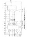
図1はこの実施の形態の光バッファ装置を示す概略的な構成図である。図1に示すようにこの実施の形態の光バッファ装置100は、4つの入力ポート10a〜10d(以下、4つの入力ポート10a〜10dをそれぞれ第1〜第4の入力ポートと称する場合がある。)と、光スイッチング手段としての光スイッチ12と、光遅延手段としての4本の光遅延線14a〜14d(以下、4本の光遅延線14a〜14dをそれぞれ第1〜第4の光遅延線と称する場合がある。)と、光結合手段としての光結合器16と、1つの出力ポート18とを具え、さらに光フィードバック手段としての1本の光フィードバック線20を具えている。また、各入力ポート10a〜10dと光スイッチ12との間には4本の光入力線22a〜22d(以下、4本の光入力線22a〜22dをそれぞれ第1〜第4の光入力線と称する場合がある。)を具え、光結合器16と出力ポート18との間には1本の光出力線24を具えている。
【0011】
このような構成のこの実施の形態の光バッファ装置100では、各入力ポート10a〜10dから入力したセルを光スイッチ12に入力させるため、第1の光入力線22aの一端は第1の入力ポート10aに接続し、第1の光入力線22aの他端は光スイッチ12の第1の入力端26aに接続してある。同様に、第2〜第4の入力線22b〜22dの一端はそれぞれ第2〜第4の入力ポート10b〜10dに接続し、第2〜第4の入力線22b〜22dの他端はそれぞれ光スイッチ12の第2〜第4の入力端26b〜26dに接続してある。
【0012】
また、光スイッチ12から出力したセルを各光遅延線14a〜14dに入力させ、さらに各光遅延線14a〜14dから出力したセルを光結合器16に入力させるため、第1の光遅延線14aの一端は光スイッチ12の第1の出力端28aに接続し、第1の光遅延線14aの他端は光結合器16の第1の入力端30aに接続してある。同様に、第2〜第4の光遅延線14b〜14dの一端はそれぞれ光スイッチ12の第2〜第4の出力端28b〜28dに接続し、第2〜第4の光遅延線14b〜14dの他端はそれぞれ光結合器16の第2〜第4の入力端30b〜30dに接続してある。ここで、第2の光遅延線14bに入力したセルは、第1の光遅延線14aに同時に入力したセルが光結合器16に到着する時間から1セル分遅延して光結合器16に到着する。同様に、第3の光遅延線14cに入力したセルは、第1の光遅延線14aに同時に入力したセルが光結合器16に到着する時間から2セル分遅延して光結合器16に到着し、第4の光遅延線14dに入力したセルは、第1の光遅延線14aに同時に入力したセルが光結合器16に到着する時間から3セル分遅延して光結合器16に到着する。
【0013】
また、光結合器16から出力したセルを出力ポート18から出力させるため、光出力線24の一端は光結合器16の出力端32に接続し、光出力線24の他端は出力ポート18に接続してある。
【0014】
また、光スイッチ12の出力側から出力したセルを光スイッチ12の入力側にフィードバックさせるため、光フィードバック線20の一端は光スイッチ12の第5の出力端28eに接続し、光フィードバック線20の他端は光スイッチ12の第5の入力端26eに接続してある。ここで、光フィードバック線20に入力したセルは、光スイッチ12の第5の出力端28eに到着した時間から1セル分遅延して光スイッチ12の第5の入力端26eに到着する。一般に、セルが光スイッチ12を通過する時間は、光フィードバック線20を通過する時間に比べて非常に短いため、光フィードバック線20に入力したセルは、1セル分遅延した後、第1〜第4の光遅延線14a〜14dに入力させることが可能となる。
【0015】
このようなこの実施の形態の光バッファ装置100は、光遅延線14a〜14d、光フィードバック線20、光入力線22a〜22d及び光出力線24として例えば光ファイバを用い、光スイッチ12として例えば2入力2出力(2×2)の単位スイッチを組み合わせて構成した6入力6出力(6×6)の光スイッチを用い、光結合器16として例えば光カプラーや、2入力2出力(2×2)の単位スイッチを組み合わせて構成した4入力4出力(4×4)の光スイッチを用いて構成することができる。この場合、光入力線を構成する光ファイバーの端部を各入力ポート10a〜10dとして用い、光出力線を構成する光ファイバーの端部を出力ポート18として用いる。また、光遅延線、及び光フィードバック線の遅延時間は光ファイバーの長さを変えて調節する。また、2×2の単位スイッチとして2×2の方向性結合器を用いると、クロス状態、バー状態の2形態を取ることができ、また動作速度が数nsと高速であるため、2×2の方向性結合器は2×2の単位スイッチとして最適である。
【0016】
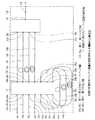
次に、このような構成のこの実施の形態の光バッファ装置100の動作について説明する。図2及び図3は、この実施の形態の光バッファ装置100の動作の説明に供する図であり、図2及び図3にはセルAが第1の入力ポート10aに、セルBが第2の入力ポート10bに、セルCが第3の入力ポート10cに、セルDが第4の入力ポート10dに同時に到着した後、さらにセルAに続いてセルEが第1の入力ポート10aに到着し、セルCに続いてセルFが第3の入力ポート10cに到着した場合について示している。すなわち、図2及び図3には、4つのセルA〜Dがそれぞれ第1〜第4の入力ポート10a〜10dに同時に到達した後、1セル分遅延して2つのセルE及びセルFがそれぞれ第1及び第3の入力ポート10a及び10cに同時に到達した場合について示している。以下、4つのセルA〜Dを先行セルと称し、2つのセルE及びFを後続セルと称する場合がある。なお、図2及び図3中、セルA〜Fは、破線または実線で表した四角形で示している。
【0017】
6つのセルA〜Fのいずれのセルもセル廃棄することなしに出力ポート18から出力させるため、先ず、4つの先行セルA〜Dが光スイッチ12に入力する時、セルAが第1の光遅延線14aに入力し、セルBが第2の光遅延線14bに入力し、セルCが第3の光遅延線14cに入力し、セルDが第4の光遅延線14dに入力するように光スイッチ12を切り替える。次に、先行セルA〜Dに続いて2つの後続セルE及びFが光スイッチ12に入力する時、セルEが第4の光遅延線14dに入力し、セルFが光フィードバック線20に入力するように光スイッチ12を切り替える(図2参照)。最後に、1セル分遅延してセルFが再度光スイッチ12に入力する時、セルFが第4の光遅延線14dに入力するように光スイッチ12を切り替える(図3参照)。このような光スイッチ12の切り替えは、各セルA〜Fのヘッダに記録されているデータに基づいて行う。すなわち、各入力ポート10a〜10dに入力する前に、各セルA〜Fのヘッダに記録されているデータを予め検出しておき、そのデータに基づいて光スイッチ12を切り替える。
【0018】
このように光スイッチ12を切り替えることにより、セルBは第2の光遅延線14bを伝達するため、セルAから1セル分遅延して出力ポート18から出力する。また、セルCは第3の光遅延線14cを伝達するため、セルAから2セル分遅延して出力ポート18から出力する。また、セルDは第4の光遅延線14dを伝達するため、セルAから3セル分遅延して出力ポート18から出力する。また、セルEはセルAから1セル分遅延して第1の入力ポート10aに到着し、その後第4の光遅延線14dを伝達するため、セルAから4セル分遅延して出力ポート18から出力する。また、セルFはセルAから1セル分遅延して第3の入力ポート10cに到着し、その後光フィードバック線20を伝達した後、第4の光遅延線14dを伝達するため、セルAから5セル分遅延して出力ポート18から出力する。
【0019】
このようにして、セルA〜Fは互いに衝突することなしに出力ポート18から出力することが可能となる。
【0020】
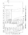
この発明は、上述した実施の形態に限定されるものではなく、トラヒックの変動に応じて、光フィードバック線の数を増やしたり、光遅延線の数を増やせば良いことは明らかである。例えば、上述した構成の光バッファ装置100の場合、4つの先行セルが同時に到着した後、連続して4つの後続セルが同時に到着すると、一部の後続セルはセル廃棄となるため、そのような場合には、図4に示す光バッファ装置の変形例110に示すように、3本の光フィードバック線20a〜20c(以下、3本の光フィードバック線20a〜20cをそれぞれ第1〜第3の光フィードバック線と称する場合がある。)を光スイッチ12の出力側から入力側に設ければ良い。より具体的には、1セル分遅延させることが可能な第1の光フィードバック線20aの一端を光スイッチ12の第5の出力端28eに他端を光スイッチ12の第5の入力端26eに接続し、2セル分遅延させることが可能な第2の光フィードバック線20bの一端を光スイッチ12の第6の出力端28fに他端を光スイッチ12の第6の入力端26fに接続し、3セル分遅延させることが可能な第3の光フィードバック線20cの一端を光スイッチ12の第7の出力端28gに他端を光スイッチ12の第7の入力端26gに接続すれば良い。このように3本の光フィードバック線20a〜20cを設けた場合には、図5及び図6に示すように、4つの先行セルA〜Dに続いて4つの後続セルE〜Hが光スイッチ12に入力する時、セルEが第4の光遅延線14dに入力し、セルFが第1の光フィードバック線20aに入力し、セルGが第2の光フィードバック線20bに入力し、セルHが第3の光フィードバック線20cに入力するように光スイッチ12を切り替える(図5参照)。そして、1セル分遅延してセルFが再度光スイッチ12に入力する時、セルFが第4の光遅延線14dに入力するように光スイッチ12を切り替え、2セル分遅延してセルGが再度光スイッチ12に入力する時、セルGが第4の光遅延線14dに入力するように光スイッチ12を切り替え、3セル分遅延してセルHが再度光スイッチ12に入力する時、セルHが第4の光遅延線14dに入力するように光スイッチ12を切り替える(図6参照)。このように光スイッチ12を切り替えることにより、セルA〜Hは互いに衝突することなしに出力ポート18から出力することが可能となる。なお、このように3本の光フィードバック線20a〜20cを光スイッチ12の出力側から入力側に設けるためには光スイッチ12の構成を変更することも必要になる。なお、図5及び図6中、セルA〜Fは、破線または実線で表した四角形で示している。
【0021】
【発明の効果】
上述した説明から明らかなように、この発明の光バッファ装置によれば、複数の入力ポートと、光スイッチ手段と、光遅延手段と、光結合手段と、1つの出力ポートとを具えた光バッファ装置において、入力ポートから同時に入力した複数の先行セルに続いて同時に複数の後続セルが入力ポートから入力する場合、光遅延手段から最後に出力した先行セルに続いて後続セルを1セルずつ時間をずらして非同時的に光遅延手段から出力させるためのフィードバック手段を光スイッチ手段の出力側から入力側に接続して設けてある。
【0022】
このような光バッファ装置によれば、光遅延手段から最後に出力した先行セルに続いて後続セルを1セルずつ時間をずらして非同時的に光遅延手段から出力させることが可能となり、従って、各セルは互いに衝突することなしに出力ポートから出力することができる。また、いずれのセルもセル廃棄することなしに出力ポートから出力させるためのハード量の増大を抑制することができる。
【図面の簡単な説明】
【図1】実施の形態の光バッファ装置を示す概略的な構成図である。
【図2】実施の形態の光バッファ装置の動作の説明に供する図(その1)である。
【図3】実施の形態の光バッファ装置の動作の説明に供する図(その2)である。
【図4】実施の形態の光バッファ装置の変形例を示す概略的な構成図である。
【図5】実施の形態の光バッファ装置の変形例の動作の説明に供する図(その1)である。
【図6】実施の形態の光バッファ装置の変形例の動作の説明に供する図(その2)である。
【図7】従来の光バッファ装置の構成及び動作の説明に供する図である。
【符号の説明】
10a〜10d:第1〜第4の入力ポート
12:光スイッチ
14a〜14d:第1〜第4の光遅延線
16:光結合器
18:出力ポート
20:光フィードバック線
20a〜20c:第1〜第3の光フィードバック線
22a〜22d:第1〜第4の光入力線
24:光出力線
26a〜26g:第1〜第7の入力端
28a〜28g:第1〜第7の出力端
30a〜30d:第1〜第4の入力端
32:出力端[0001]
BACKGROUND OF THE INVENTION
The present invention relates to an optical buffer device.
[0002]
[Prior art]
In recent years, optical technology has also been applied to the communication field, enabling high-speed and large-capacity communication. Along with this, research on optical exchange using optical technology has also been conducted in various fields in the field of switching equipment. In particular, in ATM (Asyncronus Transfer Mode) exchange, which is considered to be most effective in the future multimedia society, an optical buffer device is used to prevent fixed-length packets called cells from arriving at the same destination. Must be granted. In general, an optical buffer device uses an optical delay line composed of an optical fiber as an optical delay means (sometimes referred to as a delay memory or a delay element).
[0003]
FIG. 7 shows a conventional optical buffer device having four
[0004]
[Problems to be solved by the invention]
However, in the above-described conventional optical buffer device, when four cells A to D arrive at the same time and then two or more cells arrive at the same time, some cells are discarded. For example, as shown in FIG. 7, when four cells A to D arrive and subsequently two cells E and F arrive, the cell F cannot be processed and the cell is discarded. In order to prevent this, it is necessary to increase the size of the optical switch and further increase the number of optical delay lines. However, this method increases the amount of hardware dramatically. For example, in the case of ATM exchange, since the length of one cell is 53 bytes, if the transfer rate is 10 Gb / s, the length of the optical fiber necessary for delaying by one cell is 8 m. That's it.
[0005]
Therefore, the advent of an optical buffer device capable of avoiding cell discard without increasing the hardware amount has been desired.
[0006]
[Means for Solving the Problems]
Therefore, according to the optical buffer device of the present invention, a plurality of input ports, optical switch means, optical delay means, optical coupling means, and one output port are provided, and a cell input from the input port is optically connected. Light that is input to the switch means, the cell output from the optical switch means is input to the optical delay means, the cell output from the optical delay means is input to the optical coupling means, and the cell output from the optical coupling means is output from the output port In the buffer device, when a plurality of subsequent cells are simultaneously input from the input port following a plurality of preceding cells input simultaneously from the input port, the subsequent cells are timed one cell after the preceding cell output last from the optical delay means. A feedback means for shifting the output from the optical delay means non-simultaneously, and this feedback means is input from the output side of the optical switch means. Wherein the is provided connected to the side.
[0007]
According to such an optical buffer device, cells output from the optical switch means and input to the feedback means are delayed by a predetermined cell and input again to the optical switch means. As will be described in detail later, for example, when considering the case where two subsequent cells are simultaneously input from the input port following the four previous cells input simultaneously from the four input ports, all cells are discarded. In order to output from the output port without any input, one subsequent cell is delayed by one cell and input to the feedback means that can be input again to the optical switch means. By inputting one subsequent cell to the feedback means in this way, a delay time difference of one cell is generated between the two subsequent cells. Therefore, it is possible to output the subsequent cells from the optical delay means non-simultaneously by shifting the time by one cell after the preceding cell output last from the optical delay means. In this way, when the succeeding cells shift the time one cell at a time and output from the optical delay means non-simultaneously following the preceding cell output last from the optical delay means, the cells output without colliding with each other. Output from the port. Further, in order to output any cell from the output port without discarding the cell, the conventional optical buffer device is simply provided with a feedback means capable of delaying by one cell, so that the amount of hardware increases. Is suppressed.
[0008]
Preferably, the feedback means is composed of one or a plurality of optical fibers. Since the optical fiber can adjust the delay time of the cell that transmits the optical fiber by adjusting its length, it is suitable for use as a feedback means. In particular, when the feedback means is composed of a plurality of optical fibers and a difference in delay time of cells to be transmitted occurs between the individual optical fibers, it is possible to adapt to fluctuations in traffic.
[0009]
DETAILED DESCRIPTION OF THE INVENTION
Embodiments of the present invention will be described below with reference to the drawings. In each drawing used for the following description, each component is merely schematically shown in shape, size, and arrangement relationship to the extent that the present invention can be understood. Moreover, in each figure used for description, the same number is attached | subjected and shown about the same structural component. Therefore, it should be understood that the present invention is not limited to the embodiments described below.
[0010]
FIG. 1 is a schematic configuration diagram showing an optical buffer device according to this embodiment. As shown in FIG. 1, in the
[0011]
In the
[0012]
In addition, since the cells output from the
[0013]
In order to output the cell output from the
[0014]
Further, in order to feed back the cell output from the output side of the
[0015]
Such an
[0016]
Next, the operation of the
[0017]
In order to output any cell of the six cells A to F from the
[0018]
By switching the
[0019]
In this way, the cells A to F can output from the
[0020]
The present invention is not limited to the above-described embodiment, and it is obvious that the number of optical feedback lines or the number of optical delay lines may be increased in accordance with traffic fluctuations. For example, in the case of the
[0021]
【The invention's effect】
As is apparent from the above description, according to the optical buffer device of the present invention, an optical buffer comprising a plurality of input ports, optical switch means, optical delay means, optical coupling means, and one output port. In the apparatus, when a plurality of subsequent cells are simultaneously input from the input port following a plurality of preceding cells input simultaneously from the input port, the subsequent cells are timed one cell after the preceding cell output last from the optical delay means. Feedback means for shifting the output from the optical delay means non-simultaneously is connected from the output side of the optical switch means to the input side.
[0022]
According to such an optical buffer device, it is possible to cause the subsequent cells to be output from the optical delay means non-simultaneously by shifting the time by one cell following the preceding cell last output from the optical delay means. Each cell can be output from the output port without colliding with each other. Further, it is possible to suppress an increase in the amount of hardware for outputting any cell from the output port without discarding the cell.
[Brief description of the drawings]
FIG. 1 is a schematic configuration diagram illustrating an optical buffer device according to an embodiment;
FIG. 2 is a diagram (part 1) for explaining an operation of the optical buffer device according to the embodiment;
FIG. 3 is a diagram (part 2) for explaining the operation of the optical buffer device according to the embodiment;
FIG. 4 is a schematic configuration diagram showing a modification of the optical buffer device according to the embodiment.
FIG. 5 is a diagram (part 1) for explaining an operation of a modification of the optical buffer device according to the embodiment;
6 is a diagram (No. 2) for explaining the operation of the modification of the optical buffer device according to the embodiment; FIG.
FIG. 7 is a diagram for explaining the configuration and operation of a conventional optical buffer device;
[Explanation of symbols]
10a to 10d: First to fourth input ports 12:
Claims (1)
Translated fromJapanese前記入力ポートから同時に入力した複数の先行セルに続いて同時に複数の後続セルが前記入力ポートから入力する場合、前記光遅延手段から最後に出力した前記先行セルに続いて前記後続セルを1セルずつ時間をずらして非同時的に前記光遅延手段から出力させるためのフィードバック手段を具え、
該フィードバック手段は、前記光スイッチ手段の出力側から入力側に接続して設けてある複数本の光ファイバーで構成されており、該複数本の光ファイバーの個々の光ファイバーの間で伝達するセルの遅延時間差が生じるように構成されていることを特徴とする光バッファ装置。A plurality of input ports, optical switch means, optical delay means, optical coupling means, and one output port are provided. A cell input from the input port is input to the optical switch means, and the optical switch means In the optical buffer device for inputting the output cell to the optical delay unit, causing the cell output from the optical delay unit to be input to the optical coupling unit, and outputting the cell output from the optical coupling unit from the output port.
When a plurality of subsequent cells are simultaneously input from the input port following a plurality of preceding cells input simultaneously from the input port, the subsequent cells are placed one cell after the preceding cell output last from the optical delay means. Comprising feedback means for causing the optical delay means to output non-simultaneously at different times,
The feedback means is composed of a plurality of optical fibers connected from the output side to the input side of the optical switch means, and a delay time difference between cells transmitted between the individual optical fibers of the plurality of optical fibers. An optical buffer device characterized in that
Priority Applications (1)
| Application Number | Priority Date | Filing Date | Title |
|---|---|---|---|
| JP19229296AJP3695853B2 (en) | 1996-07-22 | 1996-07-22 | Optical buffer device |
Applications Claiming Priority (1)
| Application Number | Priority Date | Filing Date | Title |
|---|---|---|---|
| JP19229296AJP3695853B2 (en) | 1996-07-22 | 1996-07-22 | Optical buffer device |
Publications (2)
| Publication Number | Publication Date |
|---|---|
| JPH1041951A JPH1041951A (en) | 1998-02-13 |
| JP3695853B2true JP3695853B2 (en) | 2005-09-14 |
Family
ID=16288857
Family Applications (1)
| Application Number | Title | Priority Date | Filing Date |
|---|---|---|---|
| JP19229296AExpired - Fee RelatedJP3695853B2 (en) | 1996-07-22 | 1996-07-22 | Optical buffer device |
Country Status (1)
| Country | Link |
|---|---|
| JP (1) | JP3695853B2 (en) |
Families Citing this family (3)
| Publication number | Priority date | Publication date | Assignee | Title |
|---|---|---|---|---|
| US6588949B1 (en) | 1998-12-30 | 2003-07-08 | Honeywell Inc. | Method and apparatus for hermetically sealing photonic devices |
| KR100904608B1 (en)* | 2002-09-16 | 2009-06-25 | 주식회사 케이티 | Multi-wavelength optical buffer input unit control device and control method |
| WO2021176608A1 (en) | 2020-03-04 | 2021-09-10 | 日本電信電話株式会社 | Optical buffer unit, optical signal processing device, optical label switch and control method |
- 1996
- 1996-07-22JPJP19229296Apatent/JP3695853B2/ennot_activeExpired - Fee Related
Also Published As
| Publication number | Publication date |
|---|---|
| JPH1041951A (en) | 1998-02-13 |
Similar Documents
| Publication | Publication Date | Title |
|---|---|---|
| EP0547836B1 (en) | Optical packet switch | |
| US7068671B2 (en) | Multiple level minimum logic network | |
| US20190200105A1 (en) | Buffer scheduling method for flow switching | |
| US4845702A (en) | Optical telecommunication package switching system using asynchronous techniques | |
| EP0590877B1 (en) | Multistage optical packet distribution network with bypass | |
| US6934471B1 (en) | Photonic switch using time-slot interchange | |
| JPH03139044A (en) | Switch circuit net for atm system and switch circuit net module | |
| WO2002093843A1 (en) | Router | |
| JP3695853B2 (en) | Optical buffer device | |
| US5065394A (en) | Packet routing switch | |
| US5365358A (en) | Optical switching equipment for the through-connection of optical message cells | |
| US6956851B1 (en) | Crossbar subsystem and method | |
| JP3075327B2 (en) | ATM switch and ATM switching method | |
| EP0739093B1 (en) | High-speed switch and high-speed switching method | |
| JP2578946B2 (en) | Optical ATM switching system | |
| JP3589538B2 (en) | Optical buffer device and optical buffering method | |
| JPH0865318A (en) | Asynchronous transfer mode data cell routing device | |
| JPS6386938A (en) | Exchanger | |
| US20250142235A1 (en) | Optical switch fabrics for high performance computing | |
| US6577425B1 (en) | Optical device for processing a sequence of bits | |
| JP3620937B2 (en) | Optical buffer memory device | |
| JPH07283813A (en) | Output buffer type atm switch | |
| JP2855878B2 (en) | Optical self-routing circuit | |
| JP2748726B2 (en) | Optical self-routing circuit | |
| AU762271B2 (en) | Optical device for processing a sequence of bits |
Legal Events
| Date | Code | Title | Description |
|---|---|---|---|
| A977 | Report on retrieval | Free format text:JAPANESE INTERMEDIATE CODE: A971007 Effective date:20040803 | |
| A131 | Notification of reasons for refusal | Free format text:JAPANESE INTERMEDIATE CODE: A131 Effective date:20040914 | |
| A521 | Written amendment | Free format text:JAPANESE INTERMEDIATE CODE: A523 Effective date:20041028 | |
| A02 | Decision of refusal | Free format text:JAPANESE INTERMEDIATE CODE: A02 Effective date:20050222 | |
| A521 | Written amendment | Free format text:JAPANESE INTERMEDIATE CODE: A523 Effective date:20050309 | |
| A911 | Transfer to examiner for re-examination before appeal (zenchi) | Free format text:JAPANESE INTERMEDIATE CODE: A911 Effective date:20050520 | |
| TRDD | Decision of grant or rejection written | ||
| A01 | Written decision to grant a patent or to grant a registration (utility model) | Free format text:JAPANESE INTERMEDIATE CODE: A01 Effective date:20050628 | |
| A61 | First payment of annual fees (during grant procedure) | Free format text:JAPANESE INTERMEDIATE CODE: A61 Effective date:20050628 | |
| R150 | Certificate of patent or registration of utility model | Free format text:JAPANESE INTERMEDIATE CODE: R150 | |
| FPAY | Renewal fee payment (event date is renewal date of database) | Free format text:PAYMENT UNTIL: 20090708 Year of fee payment:4 | |
| FPAY | Renewal fee payment (event date is renewal date of database) | Free format text:PAYMENT UNTIL: 20100708 Year of fee payment:5 | |
| FPAY | Renewal fee payment (event date is renewal date of database) | Free format text:PAYMENT UNTIL: 20110708 Year of fee payment:6 | |
| FPAY | Renewal fee payment (event date is renewal date of database) | Free format text:PAYMENT UNTIL: 20120708 Year of fee payment:7 | |
| LAPS | Cancellation because of no payment of annual fees |