JP3693061B1 - Switching power supply - Google Patents
Switching power supplyDownload PDFInfo
- Publication number
- JP3693061B1 JP3693061B1JP2004092689AJP2004092689AJP3693061B1JP 3693061 B1JP3693061 B1JP 3693061B1JP 2004092689 AJP2004092689 AJP 2004092689AJP 2004092689 AJP2004092689 AJP 2004092689AJP 3693061 B1JP3693061 B1JP 3693061B1
- Authority
- JP
- Japan
- Prior art keywords
- transformer
- winding
- primary winding
- power supply
- secondary winding
- Prior art date
- Legal status (The legal status is an assumption and is not a legal conclusion. Google has not performed a legal analysis and makes no representation as to the accuracy of the status listed.)
- Expired - Fee Related
Links
Images


Classifications
- H—ELECTRICITY
- H02—GENERATION; CONVERSION OR DISTRIBUTION OF ELECTRIC POWER
- H02M—APPARATUS FOR CONVERSION BETWEEN AC AND AC, BETWEEN AC AND DC, OR BETWEEN DC AND DC, AND FOR USE WITH MAINS OR SIMILAR POWER SUPPLY SYSTEMS; CONVERSION OF DC OR AC INPUT POWER INTO SURGE OUTPUT POWER; CONTROL OR REGULATION THEREOF
- H02M1/00—Details of apparatus for conversion
- H02M1/32—Means for protecting converters other than automatic disconnection
- H02M1/34—Snubber circuits
- H—ELECTRICITY
- H01—ELECTRIC ELEMENTS
- H01F—MAGNETS; INDUCTANCES; TRANSFORMERS; SELECTION OF MATERIALS FOR THEIR MAGNETIC PROPERTIES
- H01F38/00—Adaptations of transformers or inductances for specific applications or functions
- H01F38/08—High-leakage transformers or inductances
- H—ELECTRICITY
- H02—GENERATION; CONVERSION OR DISTRIBUTION OF ELECTRIC POWER
- H02M—APPARATUS FOR CONVERSION BETWEEN AC AND AC, BETWEEN AC AND DC, OR BETWEEN DC AND DC, AND FOR USE WITH MAINS OR SIMILAR POWER SUPPLY SYSTEMS; CONVERSION OF DC OR AC INPUT POWER INTO SURGE OUTPUT POWER; CONTROL OR REGULATION THEREOF
- H02M3/00—Conversion of DC power input into DC power output
- H02M3/01—Resonant DC/DC converters
- H—ELECTRICITY
- H02—GENERATION; CONVERSION OR DISTRIBUTION OF ELECTRIC POWER
- H02M—APPARATUS FOR CONVERSION BETWEEN AC AND AC, BETWEEN AC AND DC, OR BETWEEN DC AND DC, AND FOR USE WITH MAINS OR SIMILAR POWER SUPPLY SYSTEMS; CONVERSION OF DC OR AC INPUT POWER INTO SURGE OUTPUT POWER; CONTROL OR REGULATION THEREOF
- H02M3/00—Conversion of DC power input into DC power output
- H02M3/22—Conversion of DC power input into DC power output with intermediate conversion into AC
- H02M3/24—Conversion of DC power input into DC power output with intermediate conversion into AC by static converters
- H02M3/28—Conversion of DC power input into DC power output with intermediate conversion into AC by static converters using discharge tubes with control electrode or semiconductor devices with control electrode to produce the intermediate AC
- H02M3/325—Conversion of DC power input into DC power output with intermediate conversion into AC by static converters using discharge tubes with control electrode or semiconductor devices with control electrode to produce the intermediate AC using devices of a triode or a transistor type requiring continuous application of a control signal
- H02M3/335—Conversion of DC power input into DC power output with intermediate conversion into AC by static converters using discharge tubes with control electrode or semiconductor devices with control electrode to produce the intermediate AC using devices of a triode or a transistor type requiring continuous application of a control signal using semiconductor devices only
- H02M3/33569—Conversion of DC power input into DC power output with intermediate conversion into AC by static converters using discharge tubes with control electrode or semiconductor devices with control electrode to produce the intermediate AC using devices of a triode or a transistor type requiring continuous application of a control signal using semiconductor devices only having several active switching elements
- H—ELECTRICITY
- H01—ELECTRIC ELEMENTS
- H01F—MAGNETS; INDUCTANCES; TRANSFORMERS; SELECTION OF MATERIALS FOR THEIR MAGNETIC PROPERTIES
- H01F27/00—Details of transformers or inductances, in general
- H01F27/28—Coils; Windings; Conductive connections
- H01F27/32—Insulating of coils, windings, or parts thereof
- H01F27/324—Insulation between coil and core, between different winding sections, around the coil; Other insulation structures
- H01F27/325—Coil bobbins
- H—ELECTRICITY
- H01—ELECTRIC ELEMENTS
- H01F—MAGNETS; INDUCTANCES; TRANSFORMERS; SELECTION OF MATERIALS FOR THEIR MAGNETIC PROPERTIES
- H01F27/00—Details of transformers or inductances, in general
- H01F27/28—Coils; Windings; Conductive connections
- H01F27/32—Insulating of coils, windings, or parts thereof
- H01F27/324—Insulation between coil and core, between different winding sections, around the coil; Other insulation structures
- H01F27/326—Insulation between coil and core, between different winding sections, around the coil; Other insulation structures specifically adapted for discharge lamp ballasts
- H—ELECTRICITY
- H01—ELECTRIC ELEMENTS
- H01F—MAGNETS; INDUCTANCES; TRANSFORMERS; SELECTION OF MATERIALS FOR THEIR MAGNETIC PROPERTIES
- H01F38/00—Adaptations of transformers or inductances for specific applications or functions
- H01F38/08—High-leakage transformers or inductances
- H01F38/10—Ballasts, e.g. for discharge lamps
- H—ELECTRICITY
- H02—GENERATION; CONVERSION OR DISTRIBUTION OF ELECTRIC POWER
- H02M—APPARATUS FOR CONVERSION BETWEEN AC AND AC, BETWEEN AC AND DC, OR BETWEEN DC AND DC, AND FOR USE WITH MAINS OR SIMILAR POWER SUPPLY SYSTEMS; CONVERSION OF DC OR AC INPUT POWER INTO SURGE OUTPUT POWER; CONTROL OR REGULATION THEREOF
- H02M1/00—Details of apparatus for conversion
- H02M1/32—Means for protecting converters other than automatic disconnection
- H02M1/34—Snubber circuits
- H02M1/342—Active non-dissipative snubbers
- Y—GENERAL TAGGING OF NEW TECHNOLOGICAL DEVELOPMENTS; GENERAL TAGGING OF CROSS-SECTIONAL TECHNOLOGIES SPANNING OVER SEVERAL SECTIONS OF THE IPC; TECHNICAL SUBJECTS COVERED BY FORMER USPC CROSS-REFERENCE ART COLLECTIONS [XRACs] AND DIGESTS
- Y02—TECHNOLOGIES OR APPLICATIONS FOR MITIGATION OR ADAPTATION AGAINST CLIMATE CHANGE
- Y02B—CLIMATE CHANGE MITIGATION TECHNOLOGIES RELATED TO BUILDINGS, e.g. HOUSING, HOUSE APPLIANCES OR RELATED END-USER APPLICATIONS
- Y02B70/00—Technologies for an efficient end-user side electric power management and consumption
- Y02B70/10—Technologies improving the efficiency by using switched-mode power supplies [SMPS], i.e. efficient power electronics conversion e.g. power factor correction or reduction of losses in power supplies or efficient standby modes
Landscapes
- Engineering & Computer Science (AREA)
- Power Engineering (AREA)
- Dc-Dc Converters (AREA)
- Coils Of Transformers For General Uses (AREA)
Abstract
Translated fromJapaneseDescription
Translated fromJapanese本発明は、高効率、小型、低ノイズなスイッチング電源装置に関するものである。 The present invention relates to a switching power supply having high efficiency, small size, and low noise.
インバータ、あるいはDC−DCコンバータ等のスイッチング電源装置に使用されるトランスとして、例えば図10に示すトランスが知られている(特許文献1)。 As a transformer used in a switching power supply device such as an inverter or a DC-DC converter, for example, a transformer shown in FIG. 10 is known (Patent Document 1).
図10に示すトランスは、外周に1次、2次巻線134,135が巻回されるコイルボビン124の胴部125の両端に、肉厚部127を有する外側フランジ128A,128Bが形成され、該外側フランジ128A,128Bの間に所定間隔をおいて複数の中間フランジ129,130,131,132,133が形成され、一方の外側フランジ128Aとこの一方の外側フランジ128Aと隣接する第1の中間フランジ129との間に1次巻線134を巻回し、第1の中間フランジ129から所定間隔をおいて設けたフランジ130と他方の外側フランジ128Bとの間に多分割して2次巻線135を巻回して1次巻線134から所定間隔離した位置に2次巻線135を巻回したものである。 In the transformer shown in FIG. 10,
このように構成したトランスは、外側フランジ128Aと第1の中間フランジ129との間に1次巻線134を巻回し、その位置から所定間隔だけ離して2次巻線135をフランジ130〜133の間毎に多分割して巻回した構造のものにおいて、1次巻線134と2次巻線135とを敢えて離した構造にすることにより、リーケージインダクタンスの量と、トランスの1次巻線及び2次巻線間の容量を変化させ、力率が最適となる値にすることができる。
しかしながら、図10に示すようなトランスにあっては、1次巻線134と2次巻線135とを所定間隔Wだけ離し、且つ2次巻線を多分割(4分割)して巻回した構造であるため、軸方向の長さが長くなり、トランスが大型化し高価となる。 However, in the transformer as shown in FIG. 10, the primary winding 134 and the secondary winding 135 are separated by a predetermined interval W and the secondary winding is wound in multiple divisions (four divisions). Due to the structure, the axial length becomes long, and the transformer becomes large and expensive.
また、1次巻線と2次巻線とを所定間隔Wだけ離しているため、1次巻線と2次巻線間のリーケージインダンタンスを適切な値に調整することができない。また、トランスの1次巻線と2次巻線間のリーケージインダンタンスをリアクトルとして使用するスイッチング電源装置が望まれていた。 Further, since the primary winding and the secondary winding are separated by a predetermined interval W, the leakage inductance between the primary winding and the secondary winding cannot be adjusted to an appropriate value. There has also been a demand for a switching power supply apparatus that uses a leakage inductance between a primary winding and a secondary winding of a transformer as a reactor.
本発明は、トランスの1次巻線と2次巻線間のリーケージインダクタンスを適切化することにより、外部のリアクトルを不要とするとともに、高効率、低ノイズで安価なスイッチング電源装置を提供することにある。 The present invention provides a switching power supply apparatus that eliminates the need for an external reactor by optimizing the leakage inductance between the primary winding and the secondary winding of the transformer, and that is highly efficient, low noise, and inexpensive. It is in.
本発明は前記課題を解決するために以下の手段を採用した。請求項1の発明は、直流電源の両端に接続され、第1リアクトルとトランスの1次巻線と主スイッチとが直列に接続された第1直列回路と、前記主スイッチの両端又は前記1次巻線の両端に接続され、補助スイッチとクランプコンデンサとが直列に接続された第2直列回路と、前記トランスの1次巻線に並列に接続された可飽和リアクトルと、前記トランスの2次巻線に発生した電圧を整流平滑する整流平滑回路と、前記主スイッチと前記補助スイッチとを交互にオン/オフさせると共に前記可飽和リアクトルの飽和により前記補助スイッチの電流が増大した時に前記補助スイッチをオフさせる制御回路とを有し、前記第1リアクトルは、前記トランスの1次巻線及び2次巻線間のリーケージインダクタンスからなり、前記トランスは、前記1次巻線を2分割して直列に接続し、前記2次巻線を2分割した1次巻線の間に配置し、2分割した1次巻線の巻数を調整することにより前記トランスの1次巻線及び2次巻線間のリーケージインダクタンスを調整したことを特徴とする。 The present invention employs the following means in order to solve the above problems. According to the first aspect of the present invention, there is provided a first series circuit in which a first reactor, a primary winding of a transformer, and a main switch are connected in series, and both ends of the main switch or the primary switch. A second series circuit connected to both ends of the winding, an auxiliary switch and a clamp capacitor connected in series, a saturable reactor connected in parallel to the primary winding of the transformer, and a secondary winding of the transformer A rectifying / smoothing circuit for rectifying and smoothing the voltage generated on the line; and alternately turning on / off the main switch and the auxiliary switch, and the auxiliary switch A control circuit for turning off, wherein the first reactor includes a leakage inductance between a primary winding and a secondary winding of the transformer, and the transformer includes the transformer The secondary winding is divided into two and connected in series, the secondary winding is arranged between the primary windings divided into two, and the number of turns of the primary winding divided into two is adjusted to adjust the number of turns of the transformer. The leakage inductance between the secondary winding and the secondary winding is adjusted.
請求項2の発明は、請求項1記載のスイッチング電源装置において、前記可飽和リアクトルは、前記トランスのコアの飽和特性を用いて形成されていることを特徴とする。 According to a second aspect of the present invention, in the switching power supply device according to the first aspect, the saturable reactor is formed using a saturation characteristic of a core of the transformer.
請求項3の発明は、請求項1又は請求項2記載のスイッチング電源装置において、前記トランスのコアの磁路の一部に断面積の少ない部分を設け、前記トランスの1次巻線及び2次巻線間のリーケージインダクタンスに蓄えられたエネルギーにより、前記トランスのコアの磁路の一部を飽和させて前記主スイッチをゼロ電圧スイッチ動作させることを特徴とする。 According to a third aspect of the present invention, in the switching power supply device according to the first or second aspect, a portion having a small cross-sectional area is provided in a part of the magnetic path of the core of the transformer, and the primary winding and the secondary of the transformer The main switch is operated as a zero voltage switch by saturating a part of the magnetic path of the core of the transformer by the energy stored in the leakage inductance between the windings.
請求項4の発明は、請求項1乃至請求項3のいずれか1項記載のスイッチング電源装置において、前記制御回路は、前記主スイッチをターンオンするときに、前記主スイッチの電圧が該主スイッチと並列に接続されたコンデンサと前記可飽和リアクトルの飽和インダクタンスとの共振によりゼロ電圧となった時から所定期間中に前記主スイッチをオンさせることを特徴とする。 According to a fourth aspect of the present invention, in the switching power supply device according to any one of the first to third aspects, when the control circuit turns on the main switch, the voltage of the main switch is different from that of the main switch. The main switch is turned on during a predetermined period from when the voltage is zero due to resonance between a capacitor connected in parallel and a saturation inductance of the saturable reactor.
請求項5の発明は、請求項1乃至請求項4のいずれか1項記載のスイッチング電源装置において、前記整流平滑回路は、前記トランスの2次巻線に直列に接続された第1整流素子と、該第1整流素子と前記2次巻線との直列回路に並列に接続された第2整流素子と、前記第2整流素子に並列に第2リアクトルを介して接続された平滑素子とを有することを特徴とする。 According to a fifth aspect of the present invention, in the switching power supply device according to any one of the first to fourth aspects, the rectifying / smoothing circuit includes a first rectifying element connected in series to the secondary winding of the transformer. A second rectifier element connected in parallel to a series circuit of the first rectifier element and the secondary winding, and a smoothing element connected in parallel to the second rectifier element via a second reactor. It is characterized by that.
請求項6の発明は、請求項1乃至請求項4のいずれか1項記載のスイッチング電源装置において、前記整流平滑回路は、前記トランスの2次巻線と3次巻線との第3直列回路と、この第3直列回路の両端に接続された第1整流素子と平滑素子との第4直列回路と、前記第2次巻線と前記3次巻線との接続点と前記第1整流素子と前記平滑素子との接続点とに接続された第2整流素子とを有することを特徴とする。 A sixth aspect of the present invention is the switching power supply device according to any one of the first to fourth aspects, wherein the rectifying and smoothing circuit is a third series circuit of a secondary winding and a tertiary winding of the transformer. A fourth series circuit of a first rectifying element and a smoothing element connected to both ends of the third series circuit, a connection point between the secondary winding and the tertiary winding, and the first rectifying element And a second rectifying element connected to a connection point with the smoothing element.
請求項7の発明は、請求項6記載のスイッチング電源装置において、前記トランスのコアには前記トランスの1次巻線と前記2次巻線とがリーケージインダクタンスをもつように巻回され、前記トランスの1次巻線と前記3次巻線とが前記1次巻線と前記2次巻線とのリーケージインダクタンスより小さなリーケージインダクタンスをもつように巻回されてなることを特徴とする。 According to a seventh aspect of the present invention, in the switching power supply device according to the sixth aspect, the transformer primary winding and the secondary winding are wound around the transformer core so as to have leakage inductance, and the transformer The primary winding and the tertiary winding are wound so as to have a leakage inductance smaller than the leakage inductance of the primary winding and the secondary winding.
本発明によれば、第1リアクトルは、トランスの1次巻線及び2次巻線間のリーケージインダクタンスからなり、トランスは、1次巻線を2分割して直列に接続し、2次巻線を2分割した1次巻線の間に配置し、2分割した1次巻線の巻数を調整することによりトランスの1次巻線及び2次巻線間のリーケージインダクタンスを調整したので、外部のリアクトルを不要とするとともに、適当なインダクタンスを1次巻線及び2次巻線間に得ることができるため、適切なゼロ電圧スイッチ動作が可能となり、高効率、低ノイズで安価なスイッチング電源装置を提供できる。 According to the present invention, the first reactor includes a leakage inductance between the primary winding and the secondary winding of the transformer, and the transformer divides the primary winding into two and connects them in series. The leakage inductance between the primary winding and the secondary winding of the transformer is adjusted by adjusting the number of turns of the primary winding divided into two and adjusting the number of turns of the primary winding divided into two. Since a reactor is not required and an appropriate inductance can be obtained between the primary and secondary windings, an appropriate zero voltage switch operation is possible, and a high-efficiency, low-noise and inexpensive switching power supply device Can be provided.
以下、本発明に係るスイッチング電源装置の実施の形態を図面を参照して詳細に説明する。 Embodiments of a switching power supply apparatus according to the present invention will be described below in detail with reference to the drawings.
実施例1のスイッチング電源装置は、主スイッチをオンした時にトランスの2次巻線を介して直接に負荷に電力を供給し、主スイッチをオフした時にトランスの1次巻線に蓄えられた励磁エネルギーをクランプコンデンサに蓄え、補助スイッチをオンすることにより、トランスのコアのB−Hカーブの第1、第3象限を使い、かつ、励磁エネルギーの不足分のエネルギーを1次巻線に接続されたリアクトルから補うことにより、B−Hカーブの出発点を第3象限の下端にすると共に、トランスの1次巻線に、可飽和リアクトルを並列に接続することにより、補助スイッチのオン期間の終了間際で可飽和リアクトルを飽和させ、電流を増大させることにより、補助スイッチのオフ時の逆電圧の発生を急峻とし、主スイッチをゼロ電圧スイッチ動作(ZVS動作)させることを特徴とする。 The switching power supply device according to the first embodiment supplies power directly to the load via the secondary winding of the transformer when the main switch is turned on, and the excitation stored in the primary winding of the transformer when the main switch is turned off. By storing energy in the clamp capacitor and turning on the auxiliary switch, the first and third quadrants of the BH curve of the transformer core are used, and the insufficient energy of the excitation energy is connected to the primary winding. By supplementing from the reactor, the starting point of the BH curve is set to the lower end of the third quadrant, and the ON period of the auxiliary switch is completed by connecting a saturable reactor in parallel to the primary winding of the transformer. Saturating the saturable reactor immediately and increasing the current makes the reverse voltage steep when the auxiliary switch is off, and the main switch operates as a zero voltage switch. Characterized in that to (ZVS operation).
また、実施例1のスイッチング電源装置は、アクティブクランプを用い、トランスの1次巻線及び2次巻線間のリーケージインダクタンスのエネルギーによって可飽和リアクトルを飽和させ、共振を利用してのスイッチング電源装置であり、トランスの1次巻線を2分割して直列に接続し、2次巻線を2分割した1次巻線の間に配置し、分割された1次巻線のそれぞれの巻数(分割した巻線の巻数の和は同一)を調整することによりトランスの1次巻線及び2次巻線間のリーケージインダクタンスを適切化し、可飽和リアクトルを飽和させ、外部のリアクトルを不要とするとともに、1次巻線及び2次巻線間の容量を減少させ、高効率、低ノイズで安価にすることを特徴とする。 In addition, the switching power supply apparatus according to the first embodiment uses an active clamp, saturates a saturable reactor with the energy of leakage inductance between the primary winding and the secondary winding of the transformer, and uses the resonance to switch the switching power supply apparatus. The primary winding of the transformer is divided into two and connected in series, and the secondary winding is arranged between the divided primary windings. The number of turns of each divided primary winding (divided) And the leakage inductance between the primary and secondary windings of the transformer is optimized to saturate the saturable reactor, eliminating the need for an external reactor, It is characterized in that the capacity between the primary winding and the secondary winding is reduced, and the efficiency and low noise are reduced.
図1は実施例1のスイッチング電源装置の回路構成図である。図1に示すスイッチング電源装置において、直流電源Vdc1の両端にはリアクトルL3とトランスTの1次巻線5a(巻数n1)とFETからなるスイッチQ1(主スイッチ)との直列回路が接続されている。スイッチQ1の両端にはダイオードD3とコンデンサC1とが並列に接続されている。なお、コンデンサC1とダイオードD3は、スイッチQ1の寄生ダイオードと寄生容量であっても良い。 FIG. 1 is a circuit configuration diagram of the switching power supply device according to the first embodiment. In the switching power supply shown in FIG. 1, a series circuit of a reactor L3, a
リアクトルL3は、トランスTの1次巻線5aと2次巻線5b間とのリーケージインダンタンスからなり、点線で示している。このリアクトルL3は、スイッチQ1がオン時にエネルギーを蓄えるとともにスイッチQ1がオフ時に蓄えられたエネルギーをクランプコンデンサC3に供給する。 Reactor L3 includes a leakage inductance between primary winding 5a and
トランスTの1次巻線5aの一端とスイッチQ1の一端との接続点にはFETからなるスイッチQ2(補助スイッチ)の一端が接続され、スイッチQ2の他端はクランプコンデンサC3を介して直流電源Vdc1の正極に接続されている。なお、スイッチQ2の他端はクランプコンデンサC3を介して直流電源Vdc1の負極に接続されていてもよい。 One end of a switch Q2 (auxiliary switch) made of FET is connected to a connection point between one end of the
スイッチQ2の両端にはダイオードD4が並列に接続されている。なお、ダイオードD4は、スイッチQ2の寄生ダイオードであっても良い。スイッチQ1,Q2は、共にオフとなる期間(デッドタイム)を有し、制御回路10のPWM制御により交互にオン/オフする。 A diode D4 is connected in parallel to both ends of the switch Q2. The diode D4 may be a parasitic diode of the switch Q2. The switches Q1, Q2 both have a period (dead time) in which they are turned off, and are alternately turned on / off by PWM control of the
トランスTの1次巻線5aの両端には、可飽和リアクトルSL1が接続されている。この可飽和リアクトルSL1は、トランスTのコアの飽和特性を用い、点線で示している。可飽和リアクトルSL1には、リーケージインダクタンス(リアクトルL3)に蓄えられたエネルギー分だけ偏ったエネルギーが供給されるため、磁束を図6に示すB−Hカーブ上の第3象限に偏磁させる電圧が印加される。 A saturable reactor SL1 is connected to both ends of the
図6に示すように一定の正磁界Hに対して磁束B(正確にはBは磁束密度であり、磁束φ=B・Sで、Sはコアの断面積であるが、ここではS=1とし、φ=Bとした。)がBmで飽和し、一定の負磁界Hに対して磁束Bが−Bmで飽和するようになっている。磁界Hは電流iの大きさに比例して発生する。この可飽和リアクトルSL1では、B−Hカーブ上を磁束BがBa→Bb→Bc→Bd→Be→Bf→Bgと移動し、磁束の動作範囲が広範囲となっている。B−Hカーブ上のBa−Bb間及びBf−Bg間は飽和状態である。 As shown in FIG. 6, the magnetic flux B (precisely, B is the magnetic flux density, magnetic flux φ = B · S, and S is the cross-sectional area of the core, but here S = 1 And φ = B.) Is saturated at Bm, and the magnetic flux B is saturated at −Bm with respect to a constant negative magnetic field H. The magnetic field H is generated in proportion to the magnitude of the current i. In the saturable reactor SL1, the magnetic flux B moves on the BH curve from Ba → Bb → Bc → Bd → Be → Bf → Bg, and the operating range of the magnetic flux is wide. Ba-Bb and Bf-Bg on the BH curve are saturated.
従って、飽和状態では、スイッチQ2の電流が増大し、この状態でスイッチQ2をオフさせることによりスイッチQ1の電圧は低下し、ゼロ電圧になる。 Therefore, in the saturated state, the current of the switch Q2 increases, and when the switch Q2 is turned off in this state, the voltage of the switch Q1 decreases and becomes zero voltage.
トランスTのコアには、1次巻線5aとこの巻線に対して同相の2次巻線5b(巻数n2)とが巻回されており、2次巻線5bの一端はダイオードD1に接続され、ダイオードD1とリアクトルL1の一端との接続点と2次巻線5bの他端とはダイオードD2に接続されており、ダイオードD1とダイオードD2とで整流回路を構成している。リアクトルL1の他端と2次巻線5bの他端とは平滑コンデンサC4に接続されている。この平滑コンデンサC4はリアクトルL1の電圧を平滑して直流出力を負荷RLに出力する。 The core of the transformer T is wound with a primary winding 5a and a secondary winding 5b (number of turns n2) in phase with the winding, and one end of the
制御回路10は、スイッチQ1とスイッチQ2とを交互にオン/オフ制御し、負荷RLの出力電圧が基準電圧以上となったときに、スイッチQ1に印加されるパルスのオン幅を狭くし、スイッチQ2に印加されるパルスのオン幅を広くするように制御する。すなわち、負荷RLの出力電圧が基準電圧以上となったときに、スイッチQ1のパルスのオン幅を狭くすることで、出力電圧を一定電圧に制御するようになっている。 The
また、制御回路10は、スイッチQ2の電流Q2iが増大した時刻にスイッチQ2をオフさせた後、スイッチQ1をオンさせる。制御回路10は、スイッチQ1をターンオンするときに、スイッチQ1の電圧がスイッチQ1と並列に接続されたコンデンサC1と可飽和リアクトルSL1の飽和インダクタンスとの共振によりゼロ電圧となった時から所定期間中にスイッチQ1をオンさせる。 Further, the
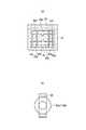
図2は実施例1のスイッチング電源装置に設けられたトランスの一例を示す図である。図2(a)はトランスの正面断面図、図2(b)はトランスの側面断面図である。図2に示すトランスは、1次巻線を2分割して直列に接続し、2次巻線を2分割した1次巻線の間に配置し、2分割した1次巻線の巻数を調整することにより、トランスの1次2次巻線間のリーケージインダクタンスを調整したものである。 FIG. 2 is a diagram illustrating an example of a transformer provided in the switching power supply device according to the first embodiment. 2A is a front sectional view of the transformer, and FIG. 2B is a side sectional view of the transformer. In the transformer shown in FIG. 2, the primary winding is divided into two parts and connected in series, and the secondary winding is arranged between the divided primary windings, and the number of turns of the divided primary winding is adjusted. Thus, the leakage inductance between the primary and secondary windings of the transformer is adjusted.
図2に示すトランスは、日の字状のコア20を有し、このコア20のコア部20aには、ボビンが設けられ、このボビンには1次巻線5aと2次巻線5bとが巻回されている。1次巻線5aは、2次巻線5bを挟んで巻線5a1と巻線5a2とに分割されて直列に接続されている。1次巻線5aの巻線5a1は、フランジ23aとフランジ23bとの間に巻回され、1次巻線5aの巻線5a2は、フランジ23cとフランジ23dとの間に巻回され、2次巻線5bは、フランジ23bとフランジ23cとの間に巻回されている。 The transformer shown in FIG. 2 has a sun-shaped
一般的に、1次巻線5aと2次巻線5b間のリーケージインダクタンスは、1次巻線5aと2次巻線5bの相対的構造が同一であれば、1次側換算のリーケージインダクタンス値をLpeとし、1次巻線5aの巻数をNpとすれば、Lpe∝Np2となる。したがって、巻数Npを1/2にすれば、リーケージインダクタンス値Lpeは1/4となる。Generally, the leakage inductance between the primary winding 5a and the secondary winding 5b is the primary side equivalent leakage inductance value if the relative structures of the primary winding 5a and the secondary winding 5b are the same. was a Lpe, if the number of turns of the primary winding 5a and Np, the LpeαNp2. Therefore, if the number of turns Np is halved, the leakage inductance value Lpe becomes ¼.
巻数Npは、コア20の断面積、入力電圧、周波数により決まる値であるため、図2に示すように、同一コア脚上に、1次巻線5aを2分割して、それぞれの巻線5a1,5a2に1/2の巻数を巻回して直列に接続すれば、1次巻線5aの巻数は同一となり、トランスTの変圧比は変化しない。 Since the number of turns Np is a value determined by the cross-sectional area of the core 20, the input voltage, and the frequency, as shown in FIG. 2, the primary winding 5a is divided into two parts on the same core leg, and the respective windings 5a1. , 5a2 are wound in half and connected in series, the number of turns of the primary winding 5a is the same, and the transformation ratio of the transformer T does not change.
この場合の1次側換算のリーケージインダクタンスLpeは、それぞれ1/4となるため、分割された2巻線を直列に接続した場合には、1次巻線5aを分割しない場合の1/2となる。ここで、Np1+Np2=Npとして巻線5a1の巻数Np1と巻線5a2の巻数Np2の比を変えた場合のリーケージインダクタンスLpcは、1次巻線5aを分割しない場合のLpcを1とすれば、(Np1/Np)2+(Np2/Np)2となり、1から1/2まで変化する。即ち、Np1とNp2の巻数比を変化させることにより、リーケージインダクタンス値を、分割しない場合の1から1/2倍まで調整することができる。In this case, the leakage inductance Lpe in terms of the primary side is 1/4, so that when the two divided windings are connected in series, the leakage inductance Lpe is 1/2 that when the primary winding 5a is not divided. Become. Here, when Np1 + Np2 = Np and the ratio of the number of turns Np1 of the winding 5a1 to the number of turns Np2 of the winding 5a2 is changed, the leakage inductance Lpc when the primary winding 5a is not divided is set to 1. Np1 / Np)2 + (Np2 / Np)2 , which varies from 1 to 1/2. That is, by changing the turn ratio of Np1 and Np2, the leakage inductance value can be adjusted from 1 to 1/2 times that in the case of not dividing.
図3は図2に示すトランスの1次巻線の巻数に対するリーケージインダクタンスの測定値の一例を示す図である。図3では、コア20の断面積が125mm2であり、1次巻線5aの巻数を34T(34ターン)とし、この巻数を2分割して、巻線5a1の巻数と巻線5a2の巻数とを変化させ(但し、2巻線5a1,5a2の巻数の合計は常に34T)、リーケージインダクタンスを測定した例である。最大のインダクタンス値と最低のインダクタンス値との比が1/2となり、理論通りになることがわかる。FIG. 3 is a diagram showing an example of a measured value of leakage inductance with respect to the number of turns of the primary winding of the transformer shown in FIG. In FIG. 3, the cross-sectional area of the
なお、1次巻線5aと2次巻線5bとの構造上の位置関係を同一とすれば、1次巻線5aを3分割以上にしても良い。この場合、1次巻線5aの分割数をNとすれば、インダクタンス値は1から1/Nまで調整することができる。 If the positional relationship in structure between the primary winding 5a and the secondary winding 5b is the same, the primary winding 5a may be divided into three or more parts. In this case, if the number of divisions of the primary winding 5a is N, the inductance value can be adjusted from 1 to 1 / N.
また、図2において、コア部20a上に、凹部20bが2箇所形成されている。この凹部20bにより、コア20の磁路の一部の断面積が他の部分よりも狭くなり、その部分のみが飽和するので、コア損失を低減できる。 In FIG. 2, two
次にこのように構成された実施例1のスイッチング電源装置の動作を図4、図5及び図7に示すタイミングチャートを参照しながら説明する。図4は実施例1のスイッチング電源装置の各部における信号のタイミングチャートである。図5は実施例1のスイッチング電源装置のスイッチQ1のターンオン時の各部における信号の詳細を示すタイミングチャートである。図6は実施例1のスイッチング電源装置に設けられたトランスのB−H特性を示す図である。図7は実施例1のスイッチング電源装置に設けられた可飽和リアクトルSL1の電流のタイミングチャートである。 Next, the operation of the switching power supply apparatus according to the first embodiment configured as described above will be described with reference to the timing charts shown in FIGS. FIG. 4 is a timing chart of signals in each part of the switching power supply device according to the first embodiment. FIG. 5 is a timing chart showing details of signals at various parts when the switch Q1 of the switching power supply device according to the first embodiment is turned on. FIG. 6 is a diagram illustrating the BH characteristics of the transformer provided in the switching power supply device according to the first embodiment. FIG. 7 is a current timing chart of the saturable reactor SL1 provided in the switching power supply device according to the first embodiment.
なお、図4及び図5では、スイッチQ1の両端間の電圧Q1v、スイッチQ1に流れる電流Q1i、スイッチQ2の両端間の電圧Q2v、スイッチQ2に流れる電流Q2i、可飽和リアクトルSL1に流れる電流SL1iを示している。 4 and 5, the voltage Q1v across the switch Q1, the current Q1i flowing through the switch Q1, the voltage Q2v across the switch Q2, the current Q2i flowing through the switch Q2, and the current SL1i flowing through the saturable reactor SL1 are shown. Show.
まず、時刻t1(時刻t11〜t12に対応)において、スイッチQ1をオンさせると、Vdcl→L3→5a→Q1→Vdc1で電流が流れる。また、この時刻に、トランスTの2次巻線5bにも電圧が発生し、5b→D1→L1→C4→5bで電流が流れる。また、スイッチQ1をオンさせた時に、リアクトルL3と可飽和リアクトルSL1に電流が流れて、リアクトルL3と可飽和リアクトルSL1にエネルギーが蓄えられる。At timet 1 (corresponding to timet 11~t 12), when to turn on the switch Q1, a current flows in Vdcl → L3 → 5a → Q1 → Vdc1. At this time, a voltage is also generated in the secondary winding 5b of the transformer T, and a current flows through 5b → D1 → L1 → C4 → 5b. When switch Q1 is turned on, current flows through reactor L3 and saturable reactor SL1, and energy is stored in reactor L3 and saturable reactor SL1.
電流SL1iは、図7に示すように、時刻t1で電流値a(負値)、時刻t1bで電流値b(負値)、時刻t13で電流値c(ゼロ)、時刻t2で電流値d(正値)へと変化していく。図6に示すB−Hカーブ上では、磁束は、Ba→Bb→Bc→Bdへと変化していく。なお、図6に示すBa〜Bgと図7に示すa〜gとは対応している。Current SL1i, as shown in FIG. 7, the current value a (negative value) at timet 1, the current value b (negative value) at timet 1 b, the current value c (zero) at timet 13, the timet 2 The current value d (positive value) changes. On the BH curve shown in FIG. 6, the magnetic flux changes from Ba → Bb → Bc → Bd. Note that Ba to Bg shown in FIG. 6 correspond to a to g shown in FIG.
次に、時刻t2において、スイッチQ1をオフさせると、リアクトルL3と可飽和リアクトルSL1とに蓄えられたエネルギーによりコンデンサC1が充電される。このとき、可飽和リアクトルSL1のインダクタンスとコンデンサC1とにより共振が形成されて、スイッチQ1の電圧Q1vが上昇する。また、L1→C4→D2→L1で電流が流れて、コンデンサC4を介して負荷RLに電流を供給する。Then, at time t2, the when to turn off the switch Q1, the capacitor C1 is charged by the energy stored in the reactor L3 and saturable reactor SL1. At this time, resonance is formed by the inductance of the saturable reactor SL1 and the capacitor C1, and the voltage Q1v of the switch Q1 increases. Further, a current flows in the order of L1, C4, D2, and L1, and the current is supplied to the load RL via the capacitor C4.
そして、コンデンサC1の電位がクランプコンデンサC3の電位と同電位となったとき、リアクトルL3と可飽和リアクトルSL1のエネルギーの放出により、ダイオードD4が導通し、電流が流れて、クランプコンデンサC3が充電されていく。また、このとき、スイッチQ2をオンさせることにより、スイッチQ2は、ゼロ電圧スイッチとなる。なお、電流SL1iは、時刻t2から時刻t20において、電流値d(正値)から電流値e(ゼロ)に変化する。図6に示すB−Hカーブ上では、磁束は、Bd→Beへと変化する。When the potential of the capacitor C1 becomes the same as the potential of the clamp capacitor C3, the diode D4 conducts due to the release of the energy of the reactor L3 and the saturable reactor SL1, the current flows, and the clamp capacitor C3 is charged. To go. At this time, when the switch Q2 is turned on, the switch Q2 becomes a zero voltage switch. The current SL1i at timet 20 from the timet 2, the change from the current value d (positive value) to the current value e (zero). On the BH curve shown in FIG. 6, the magnetic flux changes from Bd to Be.
また、リアクトルL3と可飽和リアクトルSL1とのエネルギーの放出が終了すると、クランプコンデンサC3の充電は停止する。 Further, when the release of energy from the reactor L3 and the saturable reactor SL1 is completed, the charging of the clamp capacitor C3 is stopped.
次に、時刻t20〜時刻t3において、クランプコンデンサC3に蓄えられたエネルギーは、C3→Q2→SL1(5a)→L3→C3に流れて、可飽和リアクトルSLlの磁束をリセットする。可飽和リアクトルSLlに並列に接続されたトランスTも同様に磁束が変化する。Next, at timet 20 ~ timet 3, the energy stored in the clamp capacitor C3 flows into C3 → Q2 → SL1 (5a) → L3 → C3, resets the flux of the saturable reactor SLl. Similarly, the magnetic flux of the transformer T connected in parallel to the saturable reactor SLl changes.
この場合、時刻t20〜時刻t3においては、クランプコンデンサC3に蓄えられたエネルギーが可飽和リアクトルSL1に帰還されるので、可飽和リアクトルSL1に流れる電流SL1iは、図7に示すように負値となる。即ち、電流SL1iは、時刻t20〜時刻t2aにおいては、電流値e(ゼロ)から電流値f(負値)に変化する。図6に示すB−Hカーブ上では、磁束は、Be→Bfへと変化していく。なお、時刻t2から時刻t20における面積Sと時刻t20〜時刻t2aにおける面積Sとは等しい。この面積SはクランプコンデンサC3に蓄えられた可飽和リアクトルSL1のエネルギーに相当する。In this case, at timet 20 ~ timet 3, since the energy stored in the clamp capacitor C3 is fed back to the saturable reactor SL1, current SL1i flowing through the saturable reactor SL1 is negative value as shown in FIG. 7 It becomes. That is, the current SL1i, at the timet 20 ~ timet 2a, changes from the current value e (zero) to a current value f (negative value). On the BH curve shown in FIG. 6, the magnetic flux changes from Be to Bf. Incidentally, equal to the area S of the area S and timet 20 ~ timet 2a from timet 2 at timet 20. This area S corresponds to the energy of the saturable reactor SL1 stored in the clamp capacitor C3.
次に、電流SL1iは、時刻t2a〜時刻t3においては、電流値f(負値)から電流値g(負値)に変化する。図6に示すB−Hカーブ上では、磁束は、Bf→Bgへと変化していく。時刻t2a〜時刻t3における面積は、クランプコンデンサC3に蓄えられたリアクトルL3のエネルギーに相当する。Then, current SL1i, at the timet 2a ~ timet 3, changes from current value f (negative value) to the current value g (negative value). On the BH curve shown in FIG. 6, the magnetic flux changes from Bf to Bg. Area at timet 2a ~ timet 3 corresponds to the energy of the reactor L3 accumulated in the clamp capacitor C3.
即ち、クランプコンデンサC3に蓄えられたエネルギーは、可飽和リアクトルSL1のエネルギーとリアクトルL3のエネルギーとを合わせたものであるため、電流SL1iは、リセット時にリアクトルL3から供給されるエネルギー分だけ多くなるので、磁束は第3象限に移動して、飽和領域(Bf−Bg)に達し、電流SL1iが増大し、時刻t3(時刻t1も同様)で最大となる。電流SL1iは、スイッチQ2のオン期間の終了間際で増大しており、可飽和リアクトルSL1の飽和時の飽和電流である。That is, since the energy stored in the clamp capacitor C3 is the sum of the energy of the saturable reactor SL1 and the energy of the reactor L3, the current SL1i increases by the amount of energy supplied from the reactor L3 at reset. The magnetic flux moves to the third quadrant, reaches the saturation region (Bf−Bg), increases the current SL1i, and reaches the maximum at time t3 (same as time t1 ). The current SL1i increases just before the end of the ON period of the switch Q2, and is a saturation current when the saturable reactor SL1 is saturated.
また、この時刻t3には、スイッチQ2の電流Q2iも最大となる。この時刻に、スイッチQ2をオフさせることにより、コンデンサC1の放電は急峻になり、短時間でゼロとなる。このとき、スイッチQ1をオンさせることにより、スイッチQ1はゼロ電圧スイッチを達成できる。Also, this timet 3, the current Q2i in the switch Q2 also becomes maximum. By turning off the switch Q2 at this time, the discharge of the capacitor C1 becomes steep and becomes zero in a short time. At this time, the switch Q1 can be a zero voltage switch by turning on the switch Q1.
また、飽和電流は、リアクトルL3よりクランプコンデンサC3に供給したエネルギーにより決定され、負荷が一定の場合には、流れる電流は同値であるので、リアクトルL3のインダクタンスに比例する。飽和電流が少ない場合には、スイッチQ1の電圧はゼロとならず、スイッチQ1のZVS動作が行えない。 The saturation current is determined by the energy supplied from the reactor L3 to the clamp capacitor C3. When the load is constant, the flowing current is the same value, and is proportional to the inductance of the reactor L3. When the saturation current is small, the voltage of the switch Q1 does not become zero, and the ZVS operation of the switch Q1 cannot be performed.
また、飽和電流が多い場合には、循環電流が増大し、損失が増大する。このため、リアクトルL3のインダクタンスを適当な値にする必要がある。リアクトルL3はトランスTの1次巻線5aと直列に挿入されることから、図3に示すように、トランスの1次巻線5aを2巻線5a1,5a2に分割し、分割された1次巻線5a1,5a2のそれぞれの巻数を調整することによりトランスTの1次,2次巻線間のリーケージインダクタンスを適切化して、外部のリアクトルを不要とするとともに、適当なインダクタンスを1次巻線及び2次巻線間に得ることができるため、適切なゼロ電圧スイッチ動作が可能となる。また、トランスTの1次巻線及び2次巻線間の容量を減少させることにより、高効率、低ノイズで安価で回路の簡素化を図ることができる。 Further, when the saturation current is large, the circulating current increases and the loss increases. For this reason, it is necessary to set the inductance of the reactor L3 to an appropriate value. Since the reactor L3 is inserted in series with the primary winding 5a of the transformer T, the primary winding 5a of the transformer is divided into two windings 5a1 and 5a2 as shown in FIG. By adjusting the number of turns of each of the windings 5a1 and 5a2, the leakage inductance between the primary and secondary windings of the transformer T is optimized to eliminate the need for an external reactor and provide an appropriate inductance for the primary winding. And can be obtained between the secondary windings, so that an appropriate zero voltage switch operation is possible. Further, by reducing the capacitance between the primary winding and the secondary winding of the transformer T, the circuit can be simplified with high efficiency, low noise and low cost.
次に本発明の実施例2のスイッチング電源装置を説明する。図8は実施例2のスイッチング電源装置を示す回路構成図である。図8に示す実施例2のスイッチング電源装置は、図1に示す実施例1のスイッチング電源装置に対して、トランスTaの2次側回路が異なるので、その部分についてのみ説明する。 Next, a switching power supply device according to Embodiment 2 of the present invention will be described. FIG. 8 is a circuit configuration diagram showing the switching power supply device of the second embodiment. The switching power supply device according to the second embodiment shown in FIG. 8 differs from the switching power supply device according to the first embodiment shown in FIG.
トランスTaには、1次巻線5a(巻数n1)と2次巻線5b(巻数n2)と3次巻線5c(巻数n3)が巻回されている。 A primary winding 5a (number of turns n1), a secondary winding 5b (number of turns n2), and a tertiary winding 5c (number of turns n3) are wound around the transformer Ta.
トランスTaの2次巻線5bと3次巻線5cとの直列回路の両端には、ダイオードD2と平滑コンデンサC4との直列回路が接続されている。2次巻線5bと3次巻線5cとの接続点とダイオードD2と平滑コンデンサC4との接続点とには、ダイオードD1が接続されている。1次巻線5aと2次巻線5bとは同相に巻回され、1次巻線5aと3次巻線5cとは逆相に巻回されている。 A series circuit of a diode D2 and a smoothing capacitor C4 is connected to both ends of a series circuit of the secondary winding 5b and the tertiary winding 5c of the transformer Ta. A diode D1 is connected to a connection point between the secondary winding 5b and the tertiary winding 5c and a connection point between the diode D2 and the smoothing capacitor C4. The primary winding 5a and the secondary winding 5b are wound in the same phase, and the primary winding 5a and the tertiary winding 5c are wound in opposite phases.
トランスTaの2次巻線5bを1次巻線5aと疎結合させ、1次巻線5a及び2次巻線5b間のリーケージインダクタンスにより、平滑コンデンサC4に直列に接続されるリアクトルL1を代用している。トランスTaの3次巻線5cを1次巻線5aとやや疎結合させ、1次巻線5a及び3次巻線5c間のリーケージインダクタンスにより、トランスTaに直列に接続されるリアクトルL3を代用している。 The secondary winding 5b of the transformer Ta is loosely coupled to the primary winding 5a, and the reactor L1 connected in series with the smoothing capacitor C4 is substituted by the leakage inductance between the primary winding 5a and the secondary winding 5b. ing. The tertiary winding 5c of the transformer Ta is slightly loosely coupled to the primary winding 5a, and the reactor L3 connected in series with the transformer Ta is substituted by the leakage inductance between the primary winding 5a and the tertiary winding 5c. ing.
このように構成された実施例2のスイッチング電源装置の動作を説明する。基本的な動作は、実施例1の動作と同様であり、ここでは、トランスTaの2次側回路の動作を中心に説明する。 The operation of the switching power supply device according to the second embodiment configured as described above will be described. The basic operation is the same as that of the first embodiment, and here, the operation of the secondary side circuit of the transformer Ta will be mainly described.
まず、スイッチQ1をオンさせると、Vdcl→L3→5a→Q1→Vdc1で電流が流れる。また、この時刻に、トランスTaの2次巻線5bにも電圧が発生し、5b→D1→C4→L4→5bで電流が流れる。このため、ダイオードD1の電流が直線的に増大する。 First, when the switch Q1 is turned on, a current flows through Vdc1 → L3 → 5a → Q1 → Vdc1. At this time, a voltage is also generated in the secondary winding 5b of the transformer Ta, and a current flows through 5b → D1 → C4 → L4 → 5b. For this reason, the current of the diode D1 increases linearly.
次に、スイッチQ1をオフさせると、トランスTaの1次巻線5a及び2次巻線5b間のリーケージインダクタンスL4に蓄えられたエネルギーは、トランスTaを介して2次側に還流される。2次側では、トランスTaの3次巻線5cに電圧が誘起されるため、5c→D2→C4→L4→5b→5cと電流が流れる。このため、ダイオードD2に電流が流れる。 Next, when the switch Q1 is turned off, the energy stored in the leakage inductance L4 between the primary winding 5a and the secondary winding 5b of the transformer Ta is returned to the secondary side via the transformer Ta. On the secondary side, since a voltage is induced in the tertiary winding 5c of the transformer Ta, a current flows in the order of 5c, D2, C4, L4, 5b, and 5c. For this reason, a current flows through the diode D2.
このように、トランスTaの1次巻線5a及び2次巻線5b間のリーケージインダクタンスL4の値を大きくし、スイッチQ1がオン時に蓄えられるエネルギーをトランスTaを介して2次側に還流するため、効率が良くなる。また、ダイオードD1及びダイオードD2により、スイッチQ1のオン、オフ期間に2次側電流が流れて連続的となる。このため、平滑コンデンサC4のリップル電流も減少する。 In this way, the value of the leakage inductance L4 between the primary winding 5a and the secondary winding 5b of the transformer Ta is increased, and the energy stored when the switch Q1 is turned on is returned to the secondary side via the transformer Ta. , Improve efficiency. Further, the diode D1 and the diode D2 cause the secondary current to flow and become continuous during the ON / OFF period of the switch Q1. For this reason, the ripple current of the smoothing capacitor C4 also decreases.
図9は実施例2のスイッチング電源装置に設けられたトランスの構造図である。図9(a)はトランスの正面断面図、図9(b)はトランスの側面断面図である。図9に示すトランスTaは、日の字型のコア30を有し、コア30のコア部30aには、ボビンが設けられ、このボビンには、2分割された巻線5a1,5a2からなる1次巻線5aとこの1次巻線5aに挟まれて配置された3次巻線5cとが巻回されている。1次巻線5aの巻線5a1は、フランジ33aとフランジ33bとの間に巻回され、1次巻線5aの巻線5a2は、フランジ33cとフランジ33dとの間に巻回され、3次巻線5cは、フランジ33bとフランジ33cとの間に巻回されている。これにより、1次及び3次巻線間にわずかなリーケージインダクタンスを持たせている。 FIG. 9 is a structural diagram of a transformer provided in the switching power supply device according to the second embodiment. 9A is a front sectional view of the transformer, and FIG. 9B is a side sectional view of the transformer. The transformer Ta shown in FIG. 9 has a Japanese character-shaped
また、コア30にはギャップ31が形成され、外周コア30dには2次巻線5bが巻回されている。即ち、ギャップ31により、1次巻線5aと2次巻線5bを疎結合させることにより、リーケージインダクタンスを大きくしている。 A
トランスTaのコア30にはトランスTaの1次巻線5aと2次巻線5bとがリーケージインダクタンスL4をもつように巻回され、トランスTaの1次巻線5aと3次巻線5cとがリーケージインダクタンスL3をもつように巻回され、1次巻線5aと2次巻線5bとのリーケージインダクタンスL4より小さなリーケージインダクタンスをもつように巻回されてなる。 The
また、外周コア上で且つ1次巻線5aと2次巻線5bとの間に、凹部30bが2箇所形成されている。この凹部30bにより、外周コアの磁路の一部の断面積が他の部分よりも狭くなり、その部分のみが飽和するので、コア損失を低減できる。 In addition, two
このように、トランスTaのコアの形状と巻線の工夫により、スイッチング電源装置を小型化、低価格化することができる。また、実施例1の効果と同様の効果を得ることができる。 As described above, the switching power supply device can be reduced in size and cost by the shape of the core of the transformer Ta and the device of the winding. Moreover, the same effect as the effect of Example 1 can be acquired.
本発明は、DC−DCコンバータ、AC−DCコンバータ等のスイッチング電源装置に適用可能である。 The present invention is applicable to switching power supply devices such as a DC-DC converter and an AC-DC converter.
Vdc1 直流電源
10 制御回路
Q1,Q2 スイッチ
RL 負荷
L1 リアクトル
L3,L4 リーケージインダクタンス
SL1 可飽和リアクトル
C1 コンデンサ
C3 クランプコンデンサ
C4 平滑コンデンサ
T,Ta トランス
5a 1次巻線(n1)
5a1,5a2 巻線
5b 2次巻線(n2)
5c 3次巻線(n3)
D1〜D4 ダイオード
20,30 コア
20a,30a コア部
20b,30b 凹部
23a〜23d,33a〜33d フランジ
30d 外周コア
31 ギャップVdc1
L1 Reactor L3, L4 Leakage inductance SL1 Saturable reactor C1 Capacitor C3 Clamp capacitor C4 Smoothing capacitor T,
5a1, 5a2 Winding 5b Secondary winding (n2)
5c Tertiary winding (n3)
D1-
Claims (7)
Translated fromJapanese前記主スイッチの両端又は前記1次巻線の両端に接続され、補助スイッチとクランプコンデンサとが直列に接続された第2直列回路と、
前記トランスの1次巻線に並列に接続された可飽和リアクトルと、
前記トランスの2次巻線に発生した電圧を整流平滑する整流平滑回路と、
前記主スイッチと前記補助スイッチとを交互にオン/オフさせると共に前記可飽和リアクトルの飽和により前記補助スイッチの電流が増大した時に前記補助スイッチをオフさせる制御回路とを有し、
前記第1リアクトルは、前記トランスの1次巻線及び2次巻線間のリーケージインダクタンスからなり、
前記トランスは、前記1次巻線を2分割して直列に接続し、前記2次巻線を2分割した1次巻線の間に配置し、2分割した1次巻線の巻数を調整することにより前記トランスの1次巻線及び2次巻線間のリーケージインダクタンスを調整したことを特徴とするスイッチング電源装置。A first series circuit connected to both ends of the DC power source, wherein the first reactor, the primary winding of the transformer, and the main switch are connected in series;
A second series circuit that is connected to both ends of the main switch or both ends of the primary winding, and in which an auxiliary switch and a clamp capacitor are connected in series;
A saturable reactor connected in parallel to the primary winding of the transformer;
A rectifying and smoothing circuit for rectifying and smoothing a voltage generated in the secondary winding of the transformer;
A control circuit that alternately turns on and off the main switch and the auxiliary switch and turns off the auxiliary switch when the current of the auxiliary switch increases due to saturation of the saturable reactor,
The first reactor includes a leakage inductance between the primary winding and the secondary winding of the transformer,
The transformer divides the primary winding into two and connects them in series, arranges the secondary winding between the primary windings divided into two, and adjusts the number of turns of the divided primary winding. Accordingly, the leakage inductance between the primary winding and the secondary winding of the transformer is adjusted.
The transformer primary winding and the secondary winding are wound around the transformer core so as to have leakage inductance, and the primary winding and the tertiary winding of the transformer are the primary winding. 7. The switching power supply device according to claim 6, wherein the switching power supply is wound so as to have a leakage inductance smaller than a leakage inductance between a wire and the secondary winding.
Priority Applications (5)
| Application Number | Priority Date | Filing Date | Title |
|---|---|---|---|
| JP2004092689AJP3693061B1 (en) | 2004-03-26 | 2004-03-26 | Switching power supply |
| DE112005000013TDE112005000013B4 (en) | 2004-03-26 | 2005-02-21 | Switching power supply device |
| US10/555,256US7187564B2 (en) | 2004-03-26 | 2005-02-21 | Switching power supply unit |
| CNB2005800004105ACN100433517C (en) | 2004-03-26 | 2005-02-21 | Switching power supply unit |
| PCT/JP2005/002720WO2005093935A1 (en) | 2004-03-26 | 2005-02-21 | Switching power supply unit |
Applications Claiming Priority (1)
| Application Number | Priority Date | Filing Date | Title |
|---|---|---|---|
| JP2004092689AJP3693061B1 (en) | 2004-03-26 | 2004-03-26 | Switching power supply |
Publications (2)
| Publication Number | Publication Date |
|---|---|
| JP3693061B1true JP3693061B1 (en) | 2005-09-07 |
| JP2005278380A JP2005278380A (en) | 2005-10-06 |
Family
ID=35033259
Family Applications (1)
| Application Number | Title | Priority Date | Filing Date |
|---|---|---|---|
| JP2004092689AExpired - Fee RelatedJP3693061B1 (en) | 2004-03-26 | 2004-03-26 | Switching power supply |
Country Status (5)
| Country | Link |
|---|---|
| US (1) | US7187564B2 (en) |
| JP (1) | JP3693061B1 (en) |
| CN (1) | CN100433517C (en) |
| DE (1) | DE112005000013B4 (en) |
| WO (1) | WO2005093935A1 (en) |
Cited By (1)
| Publication number | Priority date | Publication date | Assignee | Title |
|---|---|---|---|---|
| CN102820803A (en)* | 2012-06-04 | 2012-12-12 | 苏州达方电子有限公司 | Three-port single-phase single-pole micro current converter and operating method thereof |
Families Citing this family (17)
| Publication number | Priority date | Publication date | Assignee | Title |
|---|---|---|---|---|
| CN100583321C (en)* | 2006-03-25 | 2010-01-20 | 鸿富锦精密工业(深圳)有限公司 | Voltage transformer capable of adjusting leakage inductance and Electric lamp drive apparatus using same |
| JP2007267450A (en)* | 2006-03-27 | 2007-10-11 | Sanken Electric Co Ltd | Multiple-output power supply |
| JP5103832B2 (en)* | 2006-08-30 | 2012-12-19 | サンケン電気株式会社 | AC-DC converter |
| US20090153217A1 (en)* | 2007-05-08 | 2009-06-18 | Tsun-Hsiao Hsia | Active Clamp Switching Circuit |
| EP2299569B1 (en)* | 2009-09-21 | 2014-07-16 | BIONIC Engineering 5D+ AG | Direct current converter and direct current conversion method |
| WO2011048680A1 (en)* | 2009-10-22 | 2011-04-28 | イーター電機工業株式会社 | Switching power supply device |
| JP5175828B2 (en) | 2009-12-18 | 2013-04-03 | トヨタ自動車株式会社 | Fuel cell system |
| JP5563847B2 (en)* | 2010-02-26 | 2014-07-30 | 株式会社ケーヒン | Transformer and switching power supply |
| WO2013043065A2 (en)* | 2011-09-23 | 2013-03-28 | Eyales Bonifacio J | Electromagnetic energy-flux reactor |
| CN102436907B (en)* | 2011-12-22 | 2014-01-01 | 广州金升阳科技有限公司 | Magnetic core for transformer |
| US10407995B2 (en) | 2012-07-05 | 2019-09-10 | Sdg Llc | Repetitive pulsed electric discharge drills including downhole formation evaluation |
| CN103078472B (en)* | 2012-10-25 | 2015-01-07 | 中国船舶重工集团公司第七二三研究所 | Integrated integration method for magnetic assembly of high-voltage power supply of microwave power module |
| WO2015042608A1 (en)* | 2013-09-23 | 2015-03-26 | Sdg Llc | Method and apparatus for isolating and switching lower voltage pulses from high voltage pulses in electrocrushing and electrohydraulic drills |
| DE102013219533A1 (en)* | 2013-09-27 | 2015-04-02 | Siemens Aktiengesellschaft | Wireless energy technology coupling by means of an alternating magnetic field |
| CN104578768B (en)* | 2013-10-22 | 2018-10-02 | 南京中兴新软件有限责任公司 | A kind of DC power supply and its working method |
| US9584033B1 (en)* | 2015-10-19 | 2017-02-28 | Chicony Power Technology Co., Ltd. | Power supply device for varying an output voltage |
| US11515078B2 (en)* | 2016-12-21 | 2022-11-29 | Joaquín Enríque NEGRETE HERNANDEZ | Harmonics filters using semi non-magnetic bobbins |
Family Cites Families (14)
| Publication number | Priority date | Publication date | Assignee | Title |
|---|---|---|---|---|
| JP2500786B2 (en)* | 1992-11-16 | 1996-05-29 | 株式会社神戸製鋼所 | Hot rolled steel wire rod, extra fine steel wire and twisted steel wire, and method for producing extra fine steel wire |
| JPH08181023A (en)* | 1994-12-26 | 1996-07-12 | Tamura Seisakusho Co Ltd | Transformer |
| US5619400A (en)* | 1995-07-18 | 1997-04-08 | Lucent Technologies Inc. | Magnetic core structures and construction techniques therefor |
| JP3354454B2 (en)* | 1997-09-18 | 2002-12-09 | シャープ株式会社 | Switching power supply |
| JPH11186076A (en)* | 1997-12-17 | 1999-07-09 | Sanken Electric Co Ltd | Transformer |
| US6272024B2 (en)* | 1999-12-27 | 2001-08-07 | Sanken Electric Co., Ltd. | D.c.-to-d.c. converter having an improved surge suppressor |
| JP2001224170A (en)* | 2000-02-09 | 2001-08-17 | Sony Corp | Switching power circuit |
| JP2001230133A (en)* | 2000-02-16 | 2001-08-24 | Sanshin Denki Kk | Transformer unit for resonance switching power supply |
| TW521481B (en)* | 2000-05-17 | 2003-02-21 | Sony Corp | Switching power supply apparatus with active clamp circuit |
| US6466462B2 (en)* | 2000-10-31 | 2002-10-15 | Yokogawa Electric Corporation | DC/DC converter having a control circuit to reduce losses at light loads |
| JP4683364B2 (en) | 2000-12-26 | 2011-05-18 | Tdkラムダ株式会社 | Composite resonant switching power supply |
| JP4269588B2 (en)* | 2002-07-15 | 2009-05-27 | サンケン電気株式会社 | Switching power supply |
| WO2004036726A1 (en)* | 2002-10-21 | 2004-04-29 | Sanken Electric Co., Ltd. | Dc converter |
| US6856522B1 (en)* | 2003-09-13 | 2005-02-15 | Technical Witts, Inc. | Synchronous rectifier gate drive circuits for zero voltage switching power converters |
- 2004
- 2004-03-26JPJP2004092689Apatent/JP3693061B1/ennot_activeExpired - Fee Related
- 2005
- 2005-02-21CNCNB2005800004105Apatent/CN100433517C/ennot_activeExpired - Fee Related
- 2005-02-21USUS10/555,256patent/US7187564B2/ennot_activeExpired - Fee Related
- 2005-02-21DEDE112005000013Tpatent/DE112005000013B4/ennot_activeExpired - Fee Related
- 2005-02-21WOPCT/JP2005/002720patent/WO2005093935A1/enactiveApplication Filing
Cited By (2)
| Publication number | Priority date | Publication date | Assignee | Title |
|---|---|---|---|---|
| CN102820803A (en)* | 2012-06-04 | 2012-12-12 | 苏州达方电子有限公司 | Three-port single-phase single-pole micro current converter and operating method thereof |
| CN102820803B (en)* | 2012-06-04 | 2014-12-10 | 苏州达方电子有限公司 | Three-port single-phase single-pole micro current converter and operating method thereof |
Also Published As
| Publication number | Publication date |
|---|---|
| US7187564B2 (en) | 2007-03-06 |
| DE112005000013T5 (en) | 2006-07-20 |
| JP2005278380A (en) | 2005-10-06 |
| US20060209582A1 (en) | 2006-09-21 |
| DE112005000013B4 (en) | 2008-04-24 |
| CN100433517C (en) | 2008-11-12 |
| WO2005093935A1 (en) | 2005-10-06 |
| CN1788410A (en) | 2006-06-14 |
Similar Documents
| Publication | Publication Date | Title |
|---|---|---|
| JP3693061B1 (en) | Switching power supply | |
| JP3861871B2 (en) | Switching power supply | |
| US7183754B2 (en) | DC/DC converter | |
| US6807069B2 (en) | Direct current converter with integrated transformer windings and output voltage filtering coils on the same magnetic core | |
| US7983063B2 (en) | Magnetic integrated circuit for multiphase interleaved flyback converter and controlling method thereof | |
| US10211745B2 (en) | Resonant LLC converter with a multi-leg transformer with gapped center leg | |
| US8072785B2 (en) | Switching power supply unit | |
| US8223520B2 (en) | DC conversion apparatus | |
| JP4266951B2 (en) | Magnetic element and power supply device | |
| JP4175367B2 (en) | Switching power supply | |
| US20080212341A1 (en) | Dc-dc converter and transformer | |
| JPWO2018216294A1 (en) | DC / DC converter | |
| JP2016510948A (en) | Integrated magnetic transducer | |
| US7138787B2 (en) | DC/DC converter | |
| US20040218404A1 (en) | Integrated magnetic isolated two-inductor boost converter | |
| KR20130013092A (en) | Symmetric and bidirectional resonant converter | |
| JP2004297994A (en) | Isolated switching dc/dc converter | |
| JP3882809B2 (en) | Switching power supply | |
| JP5103671B2 (en) | Transformer and switching power supply device including the transformer | |
| JPWO2002052707A1 (en) | Multi-output DC-DC converter | |
| KR101229265B1 (en) | Integrated transformer and high step-up dc/dc converter using the same | |
| JP2007267450A (en) | Multiple-output power supply | |
| JPH0919135A (en) | DC / DC converter | |
| JP2004282918A (en) | DC / DC converter | |
| JP2004297995A (en) | Insulated switching dc/dc converter |
Legal Events
| Date | Code | Title | Description |
|---|---|---|---|
| TRDD | Decision of grant or rejection written | ||
| A01 | Written decision to grant a patent or to grant a registration (utility model) | Free format text:JAPANESE INTERMEDIATE CODE: A01 Effective date:20050531 | |
| A61 | First payment of annual fees (during grant procedure) | Free format text:JAPANESE INTERMEDIATE CODE: A61 Effective date:20050613 | |
| R150 | Certificate of patent or registration of utility model | Free format text:JAPANESE INTERMEDIATE CODE: R150 | |
| FPAY | Renewal fee payment (event date is renewal date of database) | Free format text:PAYMENT UNTIL: 20090701 Year of fee payment:4 | |
| FPAY | Renewal fee payment (event date is renewal date of database) | Free format text:PAYMENT UNTIL: 20100701 Year of fee payment:5 | |
| FPAY | Renewal fee payment (event date is renewal date of database) | Free format text:PAYMENT UNTIL: 20110701 Year of fee payment:6 | |
| FPAY | Renewal fee payment (event date is renewal date of database) | Free format text:PAYMENT UNTIL: 20110701 Year of fee payment:6 | |
| FPAY | Renewal fee payment (event date is renewal date of database) | Free format text:PAYMENT UNTIL: 20120701 Year of fee payment:7 | |
| FPAY | Renewal fee payment (event date is renewal date of database) | Free format text:PAYMENT UNTIL: 20130701 Year of fee payment:8 | |
| R250 | Receipt of annual fees | Free format text:JAPANESE INTERMEDIATE CODE: R250 | |
| R250 | Receipt of annual fees | Free format text:JAPANESE INTERMEDIATE CODE: R250 | |
| R250 | Receipt of annual fees | Free format text:JAPANESE INTERMEDIATE CODE: R250 | |
| R250 | Receipt of annual fees | Free format text:JAPANESE INTERMEDIATE CODE: R250 | |
| R250 | Receipt of annual fees | Free format text:JAPANESE INTERMEDIATE CODE: R250 | |
| LAPS | Cancellation because of no payment of annual fees |