JP3687452B2 - Liquid crystal display device - Google Patents
Liquid crystal display deviceDownload PDFInfo
- Publication number
- JP3687452B2 JP3687452B2JP36910099AJP36910099AJP3687452B2JP 3687452 B2JP3687452 B2JP 3687452B2JP 36910099 AJP36910099 AJP 36910099AJP 36910099 AJP36910099 AJP 36910099AJP 3687452 B2JP3687452 B2JP 3687452B2
- Authority
- JP
- Japan
- Prior art keywords
- transparent conductive
- conductive film
- electrode
- liquid crystal
- display device
- Prior art date
- Legal status (The legal status is an assumption and is not a legal conclusion. Google has not performed a legal analysis and makes no representation as to the accuracy of the status listed.)
- Expired - Fee Related
Links
Images


Landscapes
- Liquid Crystal (AREA)
- Devices For Indicating Variable Information By Combining Individual Elements (AREA)
Abstract
Description
Translated fromJapanese【0001】
【発明の属する技術分野】
本発明は液晶表示装置に係り、特に、一方の基板上に配置された画素電極と共通電極間に電圧を印加することにより両電極間に電界を形成し、液晶分子を制御することにより表示を行う液晶表示装置に関する。
【0002】
【従来の技術】
液晶表示装置として、画素を構成する表示領域にスイッチング素子として薄膜トランジスタ(TFT:Thin Film Transistor)素子を設けた構造のアクティブマトリックス方式が多く採用されている。この種の液晶表示装置においては、液晶層を一対の基板各基板で挟持した構造が採用されており、一方の基板側にはTFT素子,画素電極,各種電極,配線(走査信号,映像信号電極,配線)、及び配線と外部駆動回路とを接続するための端子等が形成され、他方の基板側にはカラーフィルタと対向電極が形成されており、基板面にほぼ垂直な縦電界を印加して表示するツイストネマチック表示方式を採用している。
【0003】
この方式に対して、液晶表示装置のネックとなっていた視野角とコントラストを改善できる方式として、カラーフィルタ基板側に配置していた対向電極に替って、TFT基板側に共通信号電極を配置し、櫛歯状の画素電極と櫛歯状の共通信号電極間に電圧を印加することにより液晶を駆動する横電界(in plain swiching)方式の液晶表示装置が、特開平6−160878 号公報に提案されている。尚、この場合には、画素電極及び共通信号電極は、メタル電極配線材料で構成してもよいし、ツイストネマチック表示方式において、透明画素電極として用いられている酸化インジウムスズ(ITO:Indium Tin Oxide)で構成してもよい。
【0004】
ITO電極を用いた例として、SID '98 DIGEST,p371(1998),及びSID '99 DIGEST,p202(1999)において、画素電極と共通信号電極とを絶縁膜を挟む上下2層のITOで構成し、櫛歯状の画素電極と共通信号電極の電極サイズ、及び電極間距離を最適化し、上下2層のITO電極間に電圧を印加して液晶を駆動する技術について記載されている。このように、画素電極と共通信号電極に透明電極を用いることにより、横電界方式の液晶表示装置の実質的な開口率,透過率が向上でき、従って、輝度を向上することができるというものである。
【0005】
【発明が解決しようとする課題】
上記従来技術において、実際に液晶表示装置を作製しようとする場合には、基板上に共通信号電極,層間絶縁膜,画素電極の順で配置された上下2層のITO電極を加工する必要がある。ITO膜の加工には、通常ウエットエッチング法が用いられる。エッチング液としては、臭化水素酸や塩酸,王水系(塩酸と硝酸の水溶液),塩化第二鉄の塩酸水溶液等、強酸の水溶液が用いられる。従って、層間絶縁膜にクラックやピンホール、付き周り部分の被覆不良等の不良部分が存在すると、層間絶縁膜を介してより上層に位置する第二のITO電極を加工する際に、この不良部分を介してITOのウエットエッチング溶液が下層に位置する第一のITO電極へ染み込むことになる。層間絶縁膜を介して下層に位置する加工済みの第一のITO電極上にこの不良部分が存在すると、染み込んだエッチング液に第一のITO電極表面が直接晒されることになり、第一のITO電極の溶解や断線不良が起こると考えられる。
【0006】
通常、TFT素子の層間絶縁膜には、CVD法で形成した窒化シリコン膜が用いられる。反応ガスとしては、例えばモノシランやアンモニア等が用いられるために、膜形成雰囲気は活性水素を含む還元プラズマ雰囲気となる。従って、ITO膜上に窒化シリコン膜を形成する際には、酸化物透明導電膜であるITO膜表面が還元プラズマ雰囲気に晒されることになる。形成条件によっては、ITO表面が還元されると共に、ITO上で窒化シリコン膜が異常成長を起こすことが知られている。(Jpn.J.Appl.Phys.,32,p5072(1993))得られた積層膜は異常成長により表面凹凸が顕著になり、窒化シリコン膜自身の緻密性,絶縁性も低下する。窒化シリコン膜の異常成長反応は、活性水素の供給源となる反応ガスの流量が多いほど、また基板温度が高いほど加速される。しかしながら、TFT素子のゲート絶縁膜用途等の良質な窒化シリコン膜を得るためには、基板温度を300度程度の高温に保つ必要があり、異常成長が起こりやすい条件で膜が形成されることになる。従って、ITO膜上に窒化シリコン膜を形成するプロセスは、上述したクラックやピンホール,付き周り部分の被覆不良等が起こりやすい状況にある。
【0007】
また、TFT素子基板側に存在する、各種メタル膜からなる電極や配線(具体的には走査信号配線、及び映像信号配線、及び共通信号配線,共通信号電極)のうち、第二のITO電極より下層に存在するメタル電極や配線についても、第一のITOと同じように、第2のITOの強酸エッチング液に晒されてしまい、腐食や溶断の可能性がある。特に、高融点メタルに比べて低抵抗な電極、もしくは配線材料として用いられるAl,Al合金膜は、耐エッチング性,耐薬品性に乏しく、ITOのエッチング液に晒されることで著しい損傷を受ける。これらの不良は、液晶表示装置の歩留まりを著しく低下させてしまう。
【0008】
本発明の目的は、画素電極又は共通信号電極として構成される2層の透明導電膜が絶縁膜を挟んで同一基板上に配置された液晶表示装置において、特にその作製時において不良が低減可能な構成の液晶表示装置を提供することにある。
【0009】
【課題を解決するための手段】
本発明の実施形態によれば、液晶層を挟持する一対の基板のいずれか一方の基板に画素電極及び共通電極を配置して、この画素電極及び共通電極に電圧を印加することにより、基板に概ね平行に(支配的に平行に)電界を発生させ、この電界により液晶分子の向きを制御して表示を行う液晶表示装置で、画素電極及び共通信号電極を、少なくとも一部が透明導電膜で異層に形成し、また、この画素電極と共通信号電極の透明導電膜は異なる組成の透明導電膜で形成し、配置した基板に対して上層に配置した透明導電膜をアモルファスの透明導電膜とし、下層に配置した透明導電膜を多結晶の透明導電膜とするというものである。
【0010】
また、別な見方の本発明の実施態様は、液晶層を挟持する一対の基板のいずれか一方の基板に画素電極及び共通電極を配置して、この画素電極及び共通電極に電圧を印加することにより、基板に概ね平行に(支配的に平行に)電界を発生させ、この電界により液晶分子の向きを制御して表示を行う液晶表示装置で、画素電極及び共通信号電極は、少なくとも一部が透明導電膜であり異層に形成し、しかもこの画素電極と共通信号電極の透明導電膜は、エッチング速度がそれぞれ異なる透明導電膜を配置するというものである。
【0011】
さらに具体的には、画素電極と共通電極の透明導電膜のエッチング速度は、配置された基板に対して上層に配置された透明導電膜が、下層に配置された透明導電膜よりエッチング速度が大きいものを使用するというものである。
【0012】
【発明の実施の形態】
以下、本発明の実施例について図面を使って説明する。
【0013】
まず、本発明の発明者は、各種透明導電膜の膜組成を変更した膜構造とエッチング挙動との関係を調査した。図23は、透明導電膜組成の一例として、酸化インジウム膜へのドープ元素をパラメータにした、酸化インジウムスズ(ITO)膜,酸化インジウム亜鉛(IZO)膜,酸化インジウムゲルマニウム(IGO)膜について本調査により得られた膜構造とエッチング特性との関係を示した図である。具体的には、これらITO,IZO,IGO膜について、膜の結晶性とエッチング液の種類をパラメータにして得られたエッチング速度について、横軸をエッチング温度(T)の逆数で整理したものである。尚、このような整理の仕方は、一般にアウレニウスプロットと呼ばれており、図中のプロットの傾きが反応の活性化エネルギーに対応する。図23中、アモルファス(amorphous)透明導電膜についてはa-、多結晶(poly crystaline)透明導電膜についてはp-、を付記して区別した。また、エッチング液の種類については、プロットの記号を変更して示した。具体的には、王水系エッチング液(HCl:HNO3:H2=1: 0.08:1)については丸、臭化水素酸水溶液(48%HBr)については四角、塩化第二鉄と塩酸の混合水溶液(39%FeCl3:HCl=1:1)については三角で示してある。いずれも、各種透明導電膜のエッチング液として一般的な、強酸系のエッチング液である。
【0014】
まず、ITO膜に着目してみると、
(1)エッチング液の温度が高くなるにつれて(1/Tの値が小さくなるにつれて)エッチング速度が大きくなること、
(2)エッチング液の強さに比例してエッチング速度が異なること(この場合、臭化水素酸系>塩化第二鉄系>王水系であるが、これらのエッチング液の濃度、及び組成比が変われば、エッチング液としての強さが変わるため、この順序が入れ替わることになる。)
(3)しかしながら、1/Tに対するエッチング速度の傾きは、エッチング液の種類,膜の結晶性が異なっていてもほぼ一定であること(これは、いずれのエッチング液,膜構造においても、溶解反応を支配する反応の活性化エネルギーが一致すること、つまり、同一の溶解反応がエッチングを律速していることを示している。)
がわかる。
【0015】
そして、最も着目すべきは、
(4)同一エッチング条件であれば、アモルファス膜のエッチング速度が、多結晶膜のエッチング速度の約100倍大きいことである。
【0016】
同じエッチング液を使用する場合においては、アモルファス膜をエッチングする場合に、多結晶膜をエッチングする場合よりも1/100にエッチング時間を短縮することができ、その分エッチング液に晒される時間を低減することができることを意味している。また、アモルファス膜のエッチング時間を多結晶膜と同等に設定するならば、その分より弱酸、または低濃度なエッチング液を使用でき、液温もより低温に設定できるため、多結晶膜に比べてホトレジスト膜や下地が被るダメージを1/100に低減でき、ダメージレスなエッチングが可能となる。弱酸のエッチング液としては、例えば、酢酸,蓚酸等の有機酸を用いることができるようになる。蓚酸溶液を用いた場合においては、強酸系のエッチング液で得られるエッチング速度に対して、約1〜2桁エッチング速度を低減することができる。そのため、液晶表示装置の電極,配線として用いられるメタル膜に対しても、同様にマイルドなエッチングが可能となる。このことは、メタル膜に対する、アモルファス透明導電膜の選択エッチングの可能性をも示唆している。メタル膜としては、液晶表示装置において、メタル電極又は配線として通常用いられている高融点金属(例えばCr,Ta,Ti,W,Mo,Nb等)、及びこれらの金属の合金膜,積層膜はもちろんのこと、より耐薬品性に劣り、溶解や腐食をより受けやすいAl,Al合金膜、及びAl,Al合金膜と高融点金属膜との積層膜を用いた場合においても、同様に、上層の透明導電膜をエッチングする際に被る損傷を低減することができる。また、塩酸や臭化水素酸等のハロゲン酸や硝酸等を用いる場合に比べて、エッチングの際のホトレジスト膜へのダメージを低減できるため、アモルファス透明導電膜自身のパターニング精度も向上でき、より微細加工が容易になる。
【0017】
次に、ITOとは膜組成の異なるIZO,IGO膜に着目する。王水系エッチング液についてのポイントデータとして示したが、a−IZO,a−IGOについても、a−ITOとほぼ同程度のエッチング速度が得られることがわかる。これより、ドープのための添加元素が、スズから亜鉛,ゲルマニウムに変わっても、膜の結晶性に対して得られるエッチング速度の効果は、ITOと同様であることがわかる。
【0018】
上記の実施例において、透明導電膜は、DCスパッタリング法、またはRFスパッタリング法において条件を変えて形成した。例えば、p−ITO膜は、インジウムに対するスズの添加量が10at%のITOターゲットを用い、スパッタリングガスはAr、または5%の酸素添加Arを用いた。(酸素の添加量は、得られるITO膜の比抵抗値が最小となる添加量に調整した。)スパッタパワーは100〜1000W、スパッタガス圧力は2〜10mTorr、基板温度は180〜350℃とした。膜厚は30〜500nmである。a−ITO膜については、スパッタリングガスはAr、または酸素添加Ar、または1%の水添加Arを用いた。(水の添加により、エッチング残さの原因となる微結晶成分の発生が抑制され、均質なアモルファス膜を得ることができる。添加量は、多すぎても少なすぎても膜の比抵抗、及び膜中の微結晶成分量を増加させてしまうため、最適値となる添加量に調整した。膜中の微結晶成分量の目安として、膜のX線回折スペクトルを測定した。a−ITO膜については、結晶成分からの回折ピークが認められないことを確認した。)スパッタパワー,スパッタガス圧力はp−ITOと同一、基板温度については、基板加熱無しで形成した。IZO,IGO膜についても、ターゲットをIZO,IGOに変更することで同様に形成した。IZO,IGO膜については、ITO膜に比べてより均質なアモルファス膜が得やすい傾向にあった。
【0019】
また、上記の実施例では、ITO膜,IZO膜,IGO膜中に添加したスズ,亜鉛,ゲルマニウムのインジウムに対する添加量(X/(In+X)、但し、In:インジウムの原子数,X:添加元素の原子数)については、10at%固定としたが、ドープ元素の添加量が3〜30at%の範囲で得られたアモルファス膜、及び多結晶膜について、上記のエッチング挙動を示すことを確認済みである。また、この添加量の範囲で得られた膜は、膜の透明導電膜としての基本特性(透過率,比抵抗特性)も良好であった。
【0020】
以上、本発明の発明者により解析された結果を、実際に液晶表示装置の透明導電膜構成に適用した。具体的には、絶縁膜を介してより上層に位置する第二の電極をアモルファスの透明導電膜で、絶縁膜を介してより下層に位置する第一の電極を多結晶の透明導電膜で構成する。つまり、第一の透明導電膜が配置された状態で、第二の透明導電膜をエッチング加工する際にも、第二の透明導電膜のエッチング速度を、第一の透明導電膜に比べて約100倍程度大きくできるため、同じエッチング液を使用する場合においては、従来に比べてエッチング時間を短縮することができ、また、エッチング時間を従来と同等にするのであれば、より弱酸、または低濃度,低温でダメージレスなエッチング液を使用することができるようになる。そのため、ピンホールや、段差部分の付き周り不良等の層間絶縁膜の不良部分を介して、第二の透明導電膜より下層に位置する第一の透明導電膜からなる電極や、メタルからなる電極,配線が、第二の透明導電膜をエッチング加工する際に被るダメージを大幅に低減することができるようになる。より望ましくは、絶縁膜を介してより上層に位置する第二の電極を、アモルファスのITO、又はアモルファスのIZO、又はアモルファスのIGOのいずれかで構成し、下層に位置する第一の電極を、液晶表示装置において透明導電膜として使用実績のある多結晶のITOで構成するとよい。
【0021】
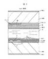
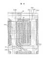
図1は、本発明の透明導電膜構成を適用した第一の実施例であるアクティブマトリックス型液晶表示装置の単位画素のTFT基板側の表面図である。図2は、図1に示したa−a′で示した線に沿う対向基板を含む断面図である。図3は、図1に示したb−b′で示した線に沿うTFT基板側の断面図である。
【0022】
図1〜図3中で、SUB1はTFT側の透明絶縁基板を、TFTは画素のスィッチング素子である薄膜トランジスタを、1は本発明の第一の透明導電膜構成からなる共通信号電極を、2は走査信号配線を、3は共通信号配線を、4はチャネル半導体となるシリコン膜を、5は映像信号配線を、6は該TFTのソース/ドレイン電極となる映像信号電極を、7は本発明の第二の透明導電膜として構成される画素電極を、8はTFTのゲート絶縁膜を、9はTFTの表面保護絶縁膜を、10はコンタクトを補償するためにリン等の不純物をドープしたシリコン膜からなる電極を示す。本実施例では、スイッチング素子として、逆スタガ型のTFTを用いている。
【0023】
図2は、図1のa−a′における対向基板をも含む断面図であり、TFT側の透明絶縁基板SUB1はTFT基板と称され、このTFT基板と、液晶LCを介して対向配置される対向側の透明絶縁基板SUB2は対向基板と称される。図2に示すように、対向基板SUB2は、液晶LC側の面に、まず、各画素領域を画するようにして遮光パターン(ブラックマトリックス)BMが形成され、この遮光パターンBMの実質的な画素領域を決定する開口部には、それを覆ってカラーフィルタFILが形成されている。そして、遮光パターンBM、及びフィルタを覆って、例えば樹脂膜からなるオーバーコート膜OCが形成され、このオーバーコート膜の上面には配向膜ORI2が形成されている。ORI1はTFT基板SUB1側の配向膜である。TFT基板SUB1,対向基板SUB2、それぞれの外側の面(液晶LC側の面とは反対の面)には、偏向板POL1,POL2が形成されている。
【0024】
図3は、図1のb−b′における断面図を示し、THは、映像信号電極(ソース・ドレイン電極)6と画素電極7とを接続するために、表面保護絶縁膜9に開口したスルーホールを示す。
【0025】
第一の実施例においては、上下2層の透明導電膜からなる電極の層間絶縁膜は、ゲート絶縁膜8とTFTの表面保護絶縁膜9との積層膜とで構成されている。これらの絶縁膜8,9を介して下層に位置する共通信号電極1は、少なくとも画素領域の周辺を除く領域に板状に形成されており、またこれらの絶縁膜8,9を介してより上層に位置する画素電極7の少なくとも一部が画素内で櫛歯状に複数に分割、またはスリット状に加工されている。本実施例において、スリット状に加工された画素電極7の電極幅、及び電極間幅は、例えばそれぞれ3μm幅とした。この画素電極7の分割、スリットの隙間部分を介して、共通信号電極1と画素電極7との間に印加される電圧により、TFT基板SUB1と対向基板SUB2間に挟持した液晶を駆動する。また、共通信号配線3については、走査信号配線2を構成するメタル膜と、同一材料,同一工程で形成した構成である。走査信号配線2、及び映像信号配線5、及び共通信号配線3を構成するメタル膜は、例えば、スパッタリング、または蒸着法等で形成されたCr,Mo,Ta,Ti,Nb,W等の高融点金属,合金、または金属シリサイド,低抵抗配線材料であるAl,Al合金、またはこれらの材料からなる積層膜で構成されている。チャネル半導体4,不純物をドープしたシリコン膜からなる電極10を構成するシリコン膜としては、例えばプラズマCVD、または熱CVD、またはスパッタリング法等で形成されたアモルファスシリコン膜、あるいは、これらの膜を熱処理、またはレーザーアニール処理して結晶化した多結晶シリコン膜が用いられる。ゲート絶縁膜8,保護絶縁膜9は、例えばプラズマCVD、またはスパッタリング法等で形成された窒化シリコン膜、または酸化シリコン膜等の絶縁膜で構成される。ゲート絶縁膜8については、走査信号配線2を構成するメタルの一部表面を酸化して得られた絶縁膜を用いてもよい。特に、チャネル半導体シリコン膜4にアモルファスシリコン膜を用いたアモルファスシリコンTFTにおいては、ゲート絶縁膜8,表面保護絶縁膜9に、プラズマCVD法で形成した窒化シリコン膜を用いている。
【0026】
課題で述べたように、ITO膜上に窒化シリコン膜を形成する際には、ITO膜表面で窒化シリコン膜が異常成長を起し、窒化シリコン膜自身の緻密性,絶縁性が低下することが知られている。そのため、クラックやピンホール,付き周り部分の被覆,絶縁不良等が起こりやすい状況にある。このような場合においても、本発明の透明導電膜構成を適用,実施することで、上層に位置する第二の透明導電膜で構成される画素電極7を、例えば蓚酸等の弱酸でエッチング加工できるようになるため、絶縁膜の不良部分を介して下層に位置する第一の透明導電膜で構成される共通信号電極1が溶解,断線することを防止できる。また、本実施例においては、上下2層の透明導電膜間に配置された層間絶縁膜の構成例として、異常成長しやすい窒化シリコン膜を例にとって説明したが、その他の絶縁膜、例えば酸化シリコン膜等を用いた場合においても同様に適用可能であり、例えば付き周り不良や、ごみ,異物、あるいは膜形成時のプラズマ放電異常等による膜質低下等で、絶縁膜に不良部分が存在する場合においても、これによる歩留りの低下を阻止することができる。また、同様に、下層に位置する走査信号電極,配線2、及び共通信号配線3の溶解,断線,腐食をも防止できる。また、上述したようにダメージレスなエッチング加工が可能となるため、低抵抗配線材料であり、透明導電膜のエッチング液に対する耐薬品性に乏しいAlやAl合金膜を、下層に位置する走査信号電極,配線2、及び共通信号配線3として使用することも可能である。但し、AlやAl合金と、酸化物である酸化インジウム系の透明導電膜が直接接触して接続部分を形成する構造では、Alと酸化物の界面において、酸化物側の酸素がAl側に移行し、絶縁膜であるアルミナ(酸化アルミニウム)膜が形成され、電気的な接続不良を起すことが知られている。従って、実際に走査信号配線2、及び共通信号配線3にAlやAl合金を適用する際には、AlやAl合金膜が透明導電膜とコンタクトを形成する側の界面に、酸素拡散を防止するための層、具体的にはCrやMo等の高融点金属膜またはその合金膜等からなる層が設けられた積層電極,配線構成となることが望ましい。また、塩酸や臭化水素酸等のハロゲン酸や硝酸等を用いる場合に比べて、アモルファス透明導電膜をエッチングする際にホトレジスト膜が被るダメージについても同様に低減できるため、透明導電膜自身のパターニング精度を向上でき、具体的には上層に位置する第二の透明導電膜で構成される画素電極7の櫛歯加工、またはスリット状加工等の微細加工が容易になる。
【0027】
尚、第一の実施例では、共通信号配線3を共通信号電極1の上部に配置した構成としたが、共通信号配線3を共通信号電極1の下部に配置する構成も勿論可能である。
【0028】
図4は、本発明の実施例に係るアクティブマトリックス型液晶表示装置の電気回路を示す概略図である。図4中x方向に延在され、y方向に併設される各走査信号配線2には、走査信号配線用端子GTMを介して、垂直走査回路Vによって順次走査信号(電圧信号)が供給されるようになっている。走査信号配線2に沿って配置される各画素領域の薄膜トランジスタTFTは走査信号によって駆動される。そして、この走査信号のタイミングに合わせて、映像信号駆動回路Hから、映像信号配線用端子DTMを介して、y方向に延在され、x方向に併設される各映像信号配線5に映像信号が供給される。この映像信号は、各画素領域の該薄膜トランジスタTFTを介して、画素電極7に印加される。各画素領域において、画素電極7と共に形成されている共通信号電極1には、共通信号配線用端子 CTMを介して共通信号配線3のバス配線CBから分岐した共通信号配線3を介して対向電圧が印加されており、これら画素電極7と共通信号電極1間に電界を発生させ液晶LCの光透過率を制御する構成である。図4中のGTMは、各走査信号配線に外部駆動回路から走査信号を供給するための走査信号配線端子を示す。なお、同図において、各画素領域に示したR,G,Bの各符号は、各画素領域にそれぞれ赤色用フィルタ,緑色用フィルタ,青色用フィルタが形成されていることを示している。
【0029】
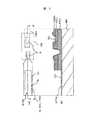
図5は、本発明の実施例に係る、アクティブマトリックス型液晶表示装置の端子部分の断面模式図を示す。TFT基板SUB1の対向基板SUB2に対する固定は、対向基板SUB2の周辺に形成されたシール材SLによってなされ、このシール材SLは、TFT基板SUB1,対向基板SUB2の間に液晶LCを封入するための封入材としての機能をも有している。このシール材SLの外側、TFT基板SUB1の周辺で、対向基板SUB2によって覆われていない領域には、それぞれ走査信号配線用端子GTM,映像信号配線用端子DTM,共通信号配線用端子CTMが形成されている。図5では、このうち、走査信号配線用端子GTMを例示してある。各端子は、導電粒子を接着剤中に分散させた異方性導電膜を介して、TCP(Tape Carrier Package)、またはCOG(Chip on Glass)接続方式により、図4で記した外部駆動回路と接続される。なお、このシール材SLの一部(図5中右側)には図示しない液晶封入口があり、ここから液晶を封入した後は液晶封入材によって封止がなされる。
【0030】
図6は、第一の実施例であるアクティブマトリックス型液晶表示装置の走査信号電極用端子GTM部分の要部平面図(a)と、(b)A−A′で示した線に沿う断面図である。
【0031】
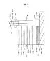
まず、透明絶縁基板SUB1上に、例えば、本発明の第一層の透明導電膜からなる端子部分を形成することで接続用のパッド電極TC1とする。そして、このパッド電極TC1には、その走査信号配線2側の端部において、走査信号配線2が覆うようにして形成されている。さらに、これらパッド電極TC1、及び走査信号配線2を覆ってゲート絶縁膜8、及び表面保護絶縁膜9が順次積層され、これらゲート絶縁膜8、及び表面保護絶縁膜9に設けた開口部THによって、第一層の透明導電膜からなるパッド電極TC1の一部が露出され、走査信号配線用端子GTMを形成する。通常、液晶表示装置の露出端子部分は、メタル材料ではなく、耐湿性,耐薬品性,腐食性に優れる透明導電膜材料で構成されるが、本実施例においても、走査信号配線用端子GTMは、耐エッチング性に優れた第一層の透明導電膜で構成されるため、露出端子部分の信頼性を十分確保できる。本実施例においては、走査信号配線2と共通信号配線1とは、同一材料,同一工程で形成されるため、図9で後述する共通信号配線用端子CTMについても、走査信号電極用端子GTMと同一材料、同一工程で形成される。
【0032】
図7は、第一の実施例であるアクティブマトリックス型液晶表示装置の、映像信号配線用端子DTM部分の要部平面図(a)と、(b)A−A′で示した線に沿う断面図である。
【0033】
映像信号配線用端子DTMにおいては、本発明の第一層の透明導電膜により端子部分を形成することで接続用のパッド電極TC1とする。このパッド電極TC1と映像信号配線5を接続する必要があるが、走査信号配線端子GTMと異なり、この間にはゲート絶縁膜層8が存在するため直接接続することができない。このため、ゲート絶縁膜8にスルーホールTHを開口して接続部分を形成する必要がある。このスルーホール開口工程を独立に行うと、ホトリソグラフィー工程が新たに必要になり工程数の増加を招く。図7は、この点を回避した映像信号用端子の構成例である。具体的には、図示はしないが走査配線用端子GTM形成工程においてもゲート絶縁膜8及び表面保護絶縁膜9に一括して開口部THを設ける工程があるが、この際に同様に映像信号配線5上及び映像信号配線用端子のパッド電極TC1上に一括してTHを形成し本発明の第二層の透明導電膜をこのパッド電極TC1と映像信号配線5を接続するための配線としてパッド電極TC2を新たに設けて、パッド電極TC1と、映像信号配線5とを接続する事で、工程数の増加という問題を回避できるというものである。映像信号配線5上では表面保護絶縁膜9のみを、映像信号配線用端子のパッド電極TC1上では、ゲート絶縁膜8と表面保護絶縁膜9との積層膜を、一括してエッチングすることになるため、映像信号配線5上の開口部はオーバーエッチング気味となるが、電気的な接続には問題が無い事を確認した。また、第一層の透明導電膜により端子部分として形成した接続用のパッド電極TC1と、第二層の透明導電膜により形成した接続用のパッド電極TC2とがスルーホールTHを介して接続される構成となるが、本発明の透明導電膜構成では、第一層目を構成する透明導電膜材料、及び第二層目を構成する透明導電膜材料として、具体的には、いずれも酸化インジウム系の透明導電膜(例えばITO,IZO,IGO)を用いているため、図1〜図3の実施例の説明で述べたAlと透明導電膜間に見られるような酸素の相互拡散によるコンタクト特性の低下は発生しない。実際に、第一層目を構成する透明導電膜材料と、第二層目を構成する透明導電膜材料とは良好なコンタクト特性が得られる事を確認済である。さらに好ましくは、第二層の透明導電膜により形成した接続用のパッド電極TC2と接続される映像信号配線5の、少なくとも表面部分については酸素拡散を防止するための層、具体的にはCrやMo合金等の高融点金属膜からなる層が設けると良い。本実施例においても、映像信号配線用端子DTMは、耐エッチング性に優れた第一層の透明導電膜で構成されるため、露出端子部分の信頼性を十分確保できる。
【0034】
図8は、図7においてTC1とTC2とを接続する際に、走査信号配線2を構成するメタル膜と同一材料,同一工程で形成したメタルのパッド電極GMPとを介して接続した実施例である。
【0035】
本発明の課題で記述したように、ゲート絶縁膜8を窒化シリコン膜で構成する場合には、本発明の第一層の透明導電膜からなるパッド電極TC1上に形成されたゲート絶縁膜8は、該パッド電極TC1と接する界面で異常成長を起こし、その部分にスルーホールTHを開口した場合、該スルーホールTHのパターン端部が逆テーパー形状に加工されることが考えられ、映像信号配線用端子DTMとの接続に不良が生じる可能性を残す事になる。そこで、図7による構成では、走査信号配線を構成するメタル膜と同一材料,同一工程で構成したパッド電極GMPを配置してこのパッド電極GMP上で、スルーホールTHの加工を行うようにした構成である。ここで、走査信号配線2を構成するメタル膜と同一材料,同一工程で構成したパッド電極GMPは、パッド電極TC1とパッド電極TC2と、電極パターンの上下で接続部分を形成しなければならず、従ってこの場合、走査信号配線2、及びパッド電極GMPは、少なくともパッド電極TC1、又はパッド電極TC2と接するパターンの上下部分が、酸素拡散を防止するための層、具体的にはCrやMo合金等の高融点金属膜からなる構成する必要がある。例えば、走査信号配線2、及びパッド電極GMPの一部に、Al,Al合金を用いた場合は、走査信号配線2、及びパッド電極GMPは、具体的にはAl合金を上下2層の高融点金属で挟んだ3層構成にすると良い。
【0036】
図9は、第一の実施例であるアクティブマトリックス型液晶表示装置の、共通信号配線用端子CTM部分の要部平面図(a)と、(b)A−A′で示した線に沿う断面図である。
【0037】
本図においては、走査信号配線2と共通信号配線3とは、同一材料,同一工程で形成されるため、共通信号配線用端子CTMについても、走査信号配線用端子GTMと同一材料,同一工程で形成される。共通信号配線用端子CTMは、走査信号配線用端子GTMとは反対の方向に引き出される他は同一構成である。
【0038】
尚、以上の第一の実施例において、ゲート絶縁膜8、及び表面保護絶縁膜9は、透明絶縁基板SUB1の周辺部分に存在する走査信号配線用端子GTM,映像信号配線用端子DTM,共通信号配線用端子CTMの露出部分を除く液晶表示装置の表示領域の全面を被覆している。
【0039】
次に、第一の実施例における各製造工程を、要部断面図を用いて説明する。
【0040】
図10は、第一の実施例であるアクティブマトリックス型液晶表示装置の(a)画素TFT部と(b)端子部の形成工程毎の断面図である。(b)の端子部の構成は、最も工程が複雑な図8の構成の映像信号配線端子DTMについて例示した。
【0041】
第一の実施例においては、具体的には(A)〜(F)の6段階のホトリソグラフィー工程を経てTFT基板SUB1が完成する。
【0042】
以下、工程順に説明する。
【0043】
工程(A)
透明絶縁基板(TFT基板SUB1となるもの)を用意し、その表面に本発明の第一層の透明導電膜として例えば多結晶ITO膜を形成する。多結晶ITO膜は、例えばスパッタリング法によって基板加熱をして形成する。次に、ホトリソグラフィー技術を用いて、この多結晶ITO膜を選択エッチングし、画素領域内には共通信号電極1を、また、映像信号配線用端子DTM形成領域には、映像信号配線用端子DTM用のパッド電極TC1を形成する。この時点では、多結晶ITO膜が第一層目であるため、エッチング液として、例えば臭化水素酸水溶液等の強酸を用いることも可能である。本実施例については、48%の臭化水素酸水溶液を用いてエッチングした。
【0044】
工程(B)
TFT基板SUB1上に、例えばスパッタリング法によってCr膜を形成する。次に、ホトリソグラフィー技術を用いてこのCr膜を選択エッチングし、画素領域内には走査信号配線2,共通信号電極1を、また映像信号配線用端子DTM形成領域には映像信号配線用端子DTM用のパッド電極GMPを形成する。
【0045】
工程(C)
TFT基板SUB1上に、例えばプラズマCVD法によってゲート絶縁膜8となる窒化シリコン膜を形成する。さらに、このゲート絶縁膜8の表面の全域に例えばプラズマCVD法によって、アモルファスシリコン膜、及びn型不純物としてリンをドーピングしたアモルファスシリコン膜を順次積層して形成する。次に、ホトリソグラフィー技術を用いてアモルファスシリコン膜を選択エッチングし、画素領域内に薄膜トランジスタTFTのチャネル半導体シリコン膜4を形成する。
【0046】
工程(D)
TFT基板SUB1上に、例えばスパッタリング法によってCr膜を形成する。次に、ホトリソグラフィー技術を用いてこのCr膜を選択エッチングし、画素領域内には薄膜トランジスタTFTのソース/ドレイン電極となる映像信号電極6、及びこの映像信号電極6の延在部である映像信号配線5を、また、映像信号配線用端子DTM形成領域には映像信号配線の延在部5を形成する。
【0047】
工程(E)
TFT基板SUB1上に、例えばプラズマCVD法によって表面保護絶縁膜9となる窒化シリコン膜を形成する。次に、ホトリソグラフィー技術を用いてこの表面保護絶縁膜9を選択的にエッチングし、画素領域内に薄膜トランジスタTFTのドレイン電極の一部を露出するためのスルーホールTHを形成する。これとともに、映像信号配線用端子DTM形成領域には、表面保護絶縁膜9の下層に位置するゲート絶縁膜8にまでスルーホールを貫通させて、映像信号配線用端子DTM用のパッド電極GMPの一部を露出させるためのスルーホールTHを形成する。
工程(F)
TFT基板SUB1上に、本発明の第二層の透明導電膜として、例えばアモルファスIZO膜を形成する。アモルファスIZO膜は、例えばスパッタリング法によって室温にて形成する。次に、ホトリソグラフィー技術を用いて、アモルファスIZO膜を選択エッチングし、画素領域内には、スルーホールTHを介して、薄膜トランジスタTFTのドレイン電極と接続された画素電極7を形成するとともに、映像信号配線用端子DTM形成領域には、第二層の透明導電膜からなる端子部分形成,接続用のパッド電極TC2を形成する。この時点では、本発明の第二層の透明導電膜であるアモルファスIZO膜が、例えば蓚酸水溶液或いは酢酸水溶液等の弱酸で十分エッチングが可能なため、ゲート絶縁膜8及び表面保護絶縁膜9に不良部分が存在しても、アモルファスIZO膜より下層に位置する第一層の透明導電膜からなる各電極、及び各メタル電極,配線が溶解断線,腐食されることを十分防止できる。本実施例については10wt%の蓚酸水溶液を用いてエッチングした。ちなみに、例えば40℃でのIZOのエッチング速度は、
2.5nm/sであった。
【0048】
図11は、本発明の透明導電膜構成を適用した第二の実施例であるアクティブマトリックス型液晶表示装置の単位画素の表面図である。
【0049】
図12は、図11に示したa−a′で示した線に沿う断面図である。図12は、図10に示したb−b′で示した線に沿う断面図である。
【0050】
第二の実施例において第一の実施例と異なる点は以下の2点である。
【0051】
(1)上下2層の透明導電膜間の層間絶縁膜が、TFTの表面保護絶縁膜9一層で構成されている点、
(2)共通信号配線11については、映像信号電極6、及び映像信号配線5を構成するメタル膜と同一材料,同一工程で形成した点、
である。
【0052】
本第二の実施例は、共通信号電極1、及び画素電極7のいずれもゲート絶縁膜8より上層に設けられているため、共通信号電極1、及び画素電極7間に電圧を印加して液晶LCを駆動する際に、ゲート絶縁膜8の厚みで生じる電圧降下分がないため、表示に寄与する電界をより効果的に得る事ができる構成である。また、共通信号電極1と画素電極7との間の層間絶縁膜についても、第一の実施例におけるゲート絶縁膜8と表面保護絶縁膜9との積層構成に比べて、ゲート絶縁膜8の単層構成としているため、共通信号電極1、及び画素電極7間で生じる電界損失についても小さくできる。本実施例においても、透明導電膜構成を適用しているため、第二の透明導電膜をエッチング加工して画素電極7を形成する際の下層に位置する映像信号電極6,映像信号配線5,共通信号配線11、及び第一の透明導電膜からなる共通信号電極1の溶解,断線を防止できる。
【0053】
図14は、第二の実施例であるアクティブマトリックス型液晶表示装置の(a)画素TFT部と(b)端子(走査信号配線端子GTM)部の形成工程毎の断面図である。
【0054】
図9の第一の実施例との形成工程との違いは、(a)の画素TFT部分については、図9における共通信号配線3が、図13においては映像信号電極(TFTのソース/ドレイン電極)6,映像信号配線5を構成するメタル膜と、同一材料,同一工程,同層に形成されていること、及び図13においては上下2層の透明電極間の層間絶縁膜が、TFTの表面保護絶縁膜9で構成されていることであり、これらの点を除けば、前述した第一の実施例における形成工程毎の断面図を示した図9と対応している。従って、(A)〜(F)で示した6回のホトリソグラフィー工程で形成可能である。しかしながら、(b)の端子部分においては、最後の工程(F)において、TFTのゲート絶縁膜8と、表面保護絶縁膜9とを一括でエッチングすることで端子部分のTHを開口する構成のため、工程(C)で形成した耐エッチング性に優れた(もしくは耐薬品性に優れた)第一の透明導電膜である多結晶ITO膜を、走査信号配線端子GTMの露出部分に適用する事ができない。従って、6回のホトリソグラフィー工程で形成した走査信号配線端子GTMは、本発明の第二の透明導電膜であるアモルファスIZO膜からなるパッド電極TC2で露出表面を被覆形成することになる。
【0055】
図15は、図14における端子露出部分についても、本発明の第一の透明導電膜構成となるように構成した例の(a)走査信号配線端子GTMと(b)映像信号配線端子DTM部の形成工程毎の断面図を示す。
【0056】
基本的には図14に示した構成に対応しており、図14と異なる点は工程(E)として、新たにスルーホール形成工程を設けて7回のホトリソグラフィー工程で形成した点である。
【0057】
工程(E)は、(a)の走査信号配線用端子GTM形成領域において、CVD法により表面保護絶縁膜9を形成し、走査信号配線2上と、接続用のパッド電極として形成しているDMP上に異なる深さのスルーホールTHを開口する工程である。
【0058】
次に、工程(F)において、工程(E)で開口した2つのスルーホールTHを利用して、第二の透明導電膜からなるパッド電極TC2を用いてこれら2つのスルーホールを接続する。これにより透明導電膜からなるパッド電極TC1と、走査信号配線2とが電気的に接続される。
【0059】
最後に、工程(G)において、本発明の第一の透明導電膜からなるパッド電極TC1で構成された走査信号配線用端子GTM上のゲート絶縁膜8と表面保護絶縁膜9との積層膜をエッチング除去,スルーホールTHを形成して端子露出部分を形成する。
【0060】
図16は、本発明の透明導電膜構成を適用した第三の実施例である、アクティブマトリックス型液晶表示装置の単位画素の表面図を、図17は、図16に示した、a−a′で示した線に沿う断面図を、図18は、図16に示した、b−b′で示した線に沿う断面図をそれぞれ示す。本実施例は、前記第二の実施例において、画素電極12を本発明の第一層(下層)の透明導電膜で、共通信号電極13を本発明の第二層(上層)の透明導電膜で構成した実施例であり、前述の実施例とは、画素電極12と共通信号電極13の上下関係を入れ替えた構成である。
【0061】
本実施例においても、本発明の第一の透明導電膜、及び本発明の第二の透明導電膜の電極としての役割及び接続先を入れ替わっただけで、本発明の第一の透明導電膜と、本発明の第二の透明導電膜との層順序関係、層構成関係には何ら変わるところがないため、上述した実施例と全く同様の効果が得られることは、言うまでもない。なお、本実施例に限らず、すべての実施例において同様に、画素電極12と共通信号電極13の上下関係を入れ替えた構成が可能である。
【0062】
図19は、本発明の透明導電膜構成を適用した第四の実施例であるアクティブマトリックス型液晶表示装置の単位画素の表面図である。
【0063】
図20は、図19に示したa−a′で示した線に沿う断面図である。図21は、図19に示したb−b′で示した線に沿う断面図である。
【0064】
第四の実施例で、第一の実施例,第二の実施例,第三の実施例と異なるのは、上下2層の透明導電膜からなる電極の層間絶縁膜がTFTのゲート絶縁膜8で構成されている点である。
【0065】
共通信号配線3については、走査信号配線2を構成するメタル膜と、同一材料,同一工程で構成している。本実施例は、最上層に位置する画素電極7も含めて、すべての電極,配線がTFTの表面保護絶縁膜9の下層に位置しており、従って、端子部分以外のすべての電極,配線が表面保護絶縁膜9で被覆されている構成である。従って、本実施例は、TFT基板SUB1が起因する液晶LCの汚染に対して有効な構成である。例えば、液晶表示装置を駆動する際の各電極,配線間の電圧差により生じる電気的腐食に起因して、各電極,配線を構成するメタル配線材料中のメタルイオンが液晶LC中に溶出して汚染されることにより、液晶LCの抵抗を低下させるモードの表示不良等に対して、相対的に強い構成であるといえる。
【0066】
図22は、第四の実施例であるアクティブマトリックス型液晶表示装置の(a)画素TFT部と(b)端子(映像信号配線端子DTM)部の形成工程毎の断面図である。
【0067】
(a)の画素TFT部分については、共通信号配線3が、走査信号配線2を構成するメタル膜と、同一材料,同一工程で形成されていること、及び第一の透明導電膜からなる共通信号電極1が走査信号配線2と同層に形成されていること、また第二の透明導電膜からなる画素電極7が映像信号電極(TFTのソース/ドレイン電極)6と同層に形成され、その結果、上下2層の透明電極間の層間絶縁膜が、TFTのゲート絶縁膜8で構成されている点を除けば、基本的には、前述した第一の実施例における、形成工程毎の断面図を示した図10と対応している。従って、(A)〜(F)で示した6回のホトリソグラフィー工程で形成できる。しかしながら、(b)の端子部分においては最後の工程(F)において、TFTのゲート絶縁膜8と表面保護絶縁膜9とを一括でエッチングすることで端子部分のTHを開口するため、最初の工程(A)で形成する耐エッチング性(もしくは耐薬品性)に優れた、本発明の第一の透明導電膜である多結晶ITO膜を、映像信号配線端子DTMの露出部分に適用する事ができない。従って、6回のホトリソグラフィー工程で形成した映像信号配線端子DTMは、本発明の第二の透明導電膜である、アモルファスIZO膜からなるパッド電極TC2で形成する。
【0068】
図23は、図22において、さらには端子露出部分についても本発明の第一の透明導電膜構成となるように構成した例の(a)走査信号配線端子GTMと(b)映像信号配線端子DTM部の形成工程毎の断面図である。
【0069】
基本的には図22に示した構成に対応しており、図22と異なる点は、工程
(D)として、新たにスルーホール形成工程を設けて、7回のホトリソグラフィー工程で形成した点である。
【0070】
工程(D)においては、(b)の走査信号配線用端子GTM形成領域では、本発明の透明導電膜からなるパッド電極TC1上に存在するゲート絶縁膜8を選択的に除去し、スルーホールTHを開口する。次に、工程(F)において、工程 (D)で開口したスルーホールTHを利用して、映像信号配線5の延在部を、パッド電極TC1に接続する。最後に、工程(G)において、本発明の第一の透明導電膜からなるパッド電極TC1で構成された映像信号配線用端子DTM上のゲート絶縁膜8と表面保護絶縁膜9との積層膜をエッチング除去,スルーホールTHを形成して端子露出部分を形成する。
【0071】
図24は、本発明の透明導電膜構成を適用した第一の実施例であるアクティブマトリックス型液晶表示装置の単位画素の表面図である。第二(上)層の透明導電膜からなる電極パターンに屈曲部を設けた実施例を示す。本実施例は、上述した各実施例を、いわゆるマルチドメイン方式の液晶表示装置に適用したものである。マルチドメイン方式とは、液晶の広がり方向に発生する電界(横電界)において、各画素領域内に該横電界の方向が異なる領域を形成するようにし、各領域の液晶分子のねじれ方向を逆にする(図24中のLC1,LC2)ことにより、例えば、表示領域を左右からそれぞれ見た場合に生じる着色差を、相殺させる効果を生じせしめたものである。具体的には、図24において、一方向に延在し、それと交差する方向に併設させた帯状の各画素電極7を、前記一方向に対して角度θ(P型液晶で、配向膜ORI1のラビング方向を映像信号配線5の方向と一致づけた場合、5〜40°の範囲が適当)に傾けて延在された後に、角度(−2θ)に屈曲させて延在させることを繰り返してジグザグ状に形成し、共通信号電極1に、絶縁膜を介して上層に、上述した構成の画素電極7が重畳するように配置させるだけで、前述したマルチドメイン方式の効果を奏することができる。そして、特に、画素電極7の屈曲部の近傍において共通信号電極1との間に発生する電界は、画素電極7の他の部分において共通信号電極1との間に発生する電界と、まったく同様に発生することが確かめられており、画素電極7の屈曲部の近傍において、光透過率の低下というような不具合を生じない効果を奏する。なお、本実施例においては、画素電極7は、図24中のy方向に延在させて形成しているが、図中のx方向に延在させるようにして、これに対して屈曲部を設けて、マルチドメインの効果を得る様にしてもよい。また、本実施例においては、画素電極7に屈曲部分を設けて、マルチドメインの効果を得るようにしたものであるが、画素電極を少なくとも画素領域の周辺を除く全領域に形成し、絶縁膜を介して上層に、上述した屈曲部を設けた構成の共通信号電極を、重畳するように配置する構成としてもよい。このようなマルチドメイン方式においても、本発明の透明導電膜構成を適用することにより、前記した所望の効果が得られることは言うまでもない。
【0072】
図25は、本発明の透明導電膜構成を適用した第一の実施例であるアクティブマトリックス型液晶表示装置の単位画素の表面図である。図25においては、第一(下)層の透明導電膜からなる電極パターンについても、櫛歯状に複数に分割加工した実施例を示している。図26は、図25に示したa−a′で示した線に沿う断面図を示す。上述した各実施例においては、いずれの場合も、絶縁膜を介して下層に位置する第一の透明導電膜からなる透明電極(共通信号電極1、または画素電極12)は、画素領域の周辺を除く全領域に形成されており、絶縁膜を介して上層に位置する第二の透明導電膜からなる透明電極(画素電極7、または共通信号電極13)のみが複数に分割、またはスリット状に加工されている構成であった。従って、第一の透明導電膜からなる透明電極(共通信号電極1、または画素電極12)と、第二の透明導電膜からなる透明電極(画素電極7、または共通信号電極13)とは、絶縁膜を介して、画素領域内のほとんどの領域に渡って重畳していることがわかる。画素電極と共通信号電極間との容量は、画素電極7,12に供給される映像信号を比較的長く蓄積させるためにある程度必要となるが、必要以上に大きくなることによって、信号の遅延による表示の輝度ばらつきが発生する。従って、画素電極と共通信号電極間との重畳面積を適当な大きさとする、あるいは画素電極と共通信号電極間の層間絶縁膜構成を最適化することによって、該容量を許容範囲内に調整する必要がある。本実施例においては、上層に位置する画素電極7のみならず、下層に位置する共通信号電極1をも複数に分割、またはスリット状に加工されており、かつ、画素電極7と共通信号電極1とは重畳しないように、並行にかみ合わさって、相互に櫛歯状に配置されているため、画素電極7と共通信号電極1間に生じる容量を考慮する必要が無い。しかしながら、この構成では、画素電極7と共通信号電極1間に電圧を印加して発生する電界には、上,下いずれの透明電極も存在しない隙間領域の分だけ、損失が生じてしまう。従って、実際には、上下2層の櫛歯電極のピッチ(電極と電極間幅を合わせた値)を同一として、上層の櫛歯電極幅,櫛歯電極間幅に対して、下層の櫛歯電極幅を相対的に太く、下層の櫛歯電極間幅を相対的に狭くして、上下2層の櫛歯電極の一部が重畳するように構成するとよい。このように構成した場合、画素電極7と共通信号電極1との間に発生する電界の分布は、全体を重畳した場合におけるそれとまったく同様にして発生させることができるため、電界を損失することなく、重畳による容量分を低減,許容範囲内とすることができる。本実施例においては、より下層に位置する、本発明の第一の透明導電膜からなる共通信号電極1についても、櫛歯状に複数に分割、またはスリット状に微細加工されているため、画素領域の周辺を除く全領域に形成した場合と比較して、断線の影響をより受けやすい状況にある。従って、本発明の透明導電膜構成を適用した際の歩留まり向上効果をより奏しやすい。
【0073】
以上の実施例においては、共通信号配線3、及び11については、走査信号配線2、或いは映像信号電極6,映像信号配線5と同層に、同一材料,同一工程で形成したメタル配線を用いているが、本発明の第一、或いは第二の透明導電膜で構成された共通信号電極1、及び13をそのまま延在して、共通電極配線として引き回してもよい。
【0074】
以上の実施例においては、本発明の透明導電膜構成を、逆スタガ型のTFTをスィッチング素子に用いた液晶表示装置に適用した例を説明したが、本発明はこれのみに限定されるものではなく、例えば正スタガ型のTFT、あるいはコプレナー型のTFT等、異なる構造のTFTを用いた場合も適用可能である。
【0075】
また、以上の実施例においては、TFTのチャネル半導体層4として、アモルファスシリコン膜を用いた例を説明したが、本発明はこれのみに限定されるものではなく、例えば多結晶シリコン膜を用いた場合においても十分適用可能である。
【0076】
【発明の効果】
本発明によれば不良が低減可能な構成の液晶表示装置を提供できる。
【図面の簡単な説明】
【図1】第一の実施例における液晶表示装置の単位画素の表面図である。
【図2】図1に示したa−a′断面図である。
【図3】図1に示したb−b′断面図である。
【図4】本発明の実施例に係る液晶表示装置の電気回路を示す概略図である。
【図5】本発明の実施例に係る液晶表示装置の端子部分の断面模式図である。
【図6】第一の実施例における走査信号配線端子部分の要部平面図及び断面図である。
【図7】第一の実施例における映像信号配線端子部分の要部平面図及び断面図である。
【図8】第一の実施例における共通信号配線端子部分の要部平面図及び断面図である。
【図9】第一の実施例における共通信号配線端子部分の要部平面図及び断面図である。
【図10】第一の実施例における画素TFT部及び映像信号配線端子部の形成工程毎の断面図である。
【図11】第二の実施例における液晶表示装置の単位画素の表面図である。
【図12】図11に示したa−a′断面図である。
【図13】図11に示したb−b′断面図である。
【図14】第二の実施例における液晶表示装置の画素TFT部と走査信号配線端子部の形成工程毎の断面図である。
【図15】第二の実施例において、端子露出部分についても透明導電膜構成となるように構成した例の走査信号配線端子部と映像信号配線端子部の形成工程毎の断面図である。
【図16】第三の実施例における液晶表示装置の単位画素の表面図(第二の実施例の画素電極を第一(下)層に、共通信号電極を第二(上)層で形成)である。
【図17】図16に示したa−a′断面図である。
【図18】図16に示したb−b′断面図である。
【図19】第四の実施例における液晶表示装置の単位画素の表面図である。
【図20】図19に示したa−a′断面図である。
【図21】図19に示したb−b′断面図である。
【図22】第四の実施例における液晶表示装置の画素TFT部及び映像信号配線端子部の形成工程毎の断面図である。
【図23】第四の実施例において、端子露出部分についても透明導電膜構成となるように構成した例の走査信号配線端子部と映像信号配線端子部の形成工程毎の断面図である。
【図24】本発明において、第二(上)層の透明導電膜の電極パターンを屈曲部を設けた構成とした例を示す図である。
【図25】本発明において、第一(下)層の透明導電膜からなる電極パターンについても櫛歯状に複数に分割加工した例を示す図である。
【図26】図25に示したa−a′断面図である。
【図27】本発明を構成する各種透明導電膜のエッチング特性を示す説明図である。
【符号の説明】
1,13…共通信号電極、2…走査信号配線、3、11…共通信号配線、4…チャネル半導体シリコン膜、5…映像信号配線、6…映像信号電極(ソース・ドレイン電極)、7,12…画素電極、8…ゲート絶縁膜、9…TFTの表面保護絶縁膜、10…不純物を導入したシリコン膜からなる電極、TFT…薄膜トランジスタ、TH…絶縁膜に開口したスルーホール、SUB1,SUB2…透明絶縁基板、GTM…走査信号配線用端子、DTM…映像信号配線用端子、CTM…共通信号配線用端子、CB…共通信号配線のバス配線、TC1…第一層の透明導電膜により形成した端子部分を形成する接続用のパッド電極、TC2…第二層の透明導電膜により形成した端子部分を形成する接続用のパッド電極、GMP…走査信号配線を構成するメタル膜と同一材料,同一工程で構成した端子部分を形成する接続用のパッド電極、DMP…映像信号配線を構成するメタル膜と同一材料,同一工程で構成した端子部分を形成する接続用のパッド電極。[0001]
BACKGROUND OF THE INVENTION
The present invention relates to a liquid crystal display device, and in particular, a voltage is applied between a pixel electrode and a common electrode arranged on one substrate to form an electric field between the two electrodes, and display is performed by controlling liquid crystal molecules. The present invention relates to a liquid crystal display device.
[0002]
[Prior art]
As a liquid crystal display device, an active matrix system having a structure in which a thin film transistor (TFT) element is provided as a switching element in a display region constituting a pixel is often used. In this type of liquid crystal display device, a structure in which a liquid crystal layer is sandwiched between a pair of substrates is employed. On one substrate side, a TFT element, a pixel electrode, various electrodes, and wiring (scanning signal, video signal electrode) , Wiring), and terminals for connecting the wiring and the external drive circuit are formed, and a color filter and a counter electrode are formed on the other substrate side, and a vertical electric field substantially perpendicular to the substrate surface is applied. The twist nematic display method is used.
[0003]
In contrast to this method, a common signal electrode is arranged on the TFT substrate side instead of the counter electrode arranged on the color filter substrate side as a method that can improve the viewing angle and contrast that have been the bottleneck of the liquid crystal display device. Japanese Patent Laid-Open No. 6-160878 discloses an in-plane switching type liquid crystal display device that drives a liquid crystal by applying a voltage between a comb-like pixel electrode and a comb-like common signal electrode. Proposed. In this case, the pixel electrode and the common signal electrode may be made of a metal electrode wiring material, or indium tin oxide (ITO) used as a transparent pixel electrode in the twisted nematic display system. ).
[0004]
As an example using ITO electrodes, in SID '98 DIGEST, p371 (1998) and SID '99 DIGEST, p202 (1999), the pixel electrode and the common signal electrode are composed of two layers of ITO with an insulating film sandwiched between them. A technique for optimizing the electrode size of the comb-like pixel electrode and the common signal electrode and the distance between the electrodes and applying a voltage between the upper and lower ITO electrodes to drive the liquid crystal is described. Thus, by using a transparent electrode for the pixel electrode and the common signal electrode, the substantial aperture ratio and transmittance of the horizontal electric field type liquid crystal display device can be improved, and therefore the luminance can be improved. is there.
[0005]
[Problems to be solved by the invention]
In the above prior art, when actually manufacturing a liquid crystal display device, it is necessary to process the upper and lower ITO electrodes arranged in the order of the common signal electrode, the interlayer insulating film, and the pixel electrode on the substrate. . A wet etching method is usually used for processing the ITO film. As the etchant, an aqueous solution of strong acid such as hydrobromic acid, hydrochloric acid, aqua regia system (aqueous solution of hydrochloric acid and nitric acid), aqueous hydrochloric acid solution of ferric chloride and the like is used. Therefore, when there are defective portions such as cracks, pinholes, and poor coverage of the surrounding portions in the interlayer insulating film, when the second ITO electrode located in the upper layer is processed through the interlayer insulating film, this defective portion Through this, the ITO wet etching solution penetrates into the first ITO electrode located in the lower layer. If this defective portion exists on the processed first ITO electrode located in the lower layer through the interlayer insulating film, the surface of the first ITO electrode is directly exposed to the soaked etching solution, and the first ITO It is thought that electrode dissolution or disconnection failure occurs.
[0006]
Usually, a silicon nitride film formed by a CVD method is used as an interlayer insulating film of a TFT element. As the reactive gas, for example, monosilane, ammonia or the like is used, so that the film forming atmosphere is a reducing plasma atmosphere containing active hydrogen. Therefore, when the silicon nitride film is formed on the ITO film, the surface of the ITO film, which is an oxide transparent conductive film, is exposed to a reducing plasma atmosphere. It is known that depending on the formation conditions, the ITO surface is reduced and the silicon nitride film causes abnormal growth on the ITO. (Jpn. J. Appl. Phys., 32, p5072 (1993)) The resulting laminated film has surface irregularities due to abnormal growth, and the denseness and insulation of the silicon nitride film itself are also reduced. The abnormal growth reaction of the silicon nitride film is accelerated as the flow rate of the reactive gas serving as the supply source of active hydrogen increases and as the substrate temperature increases. However, in order to obtain a high-quality silicon nitride film for use in a gate insulating film of a TFT element, it is necessary to keep the substrate temperature at a high temperature of about 300 ° C., and the film is formed under conditions where abnormal growth easily occurs. Become. Therefore, the process of forming the silicon nitride film on the ITO film is in a situation where the above-described cracks, pinholes, defective coating of the surrounding portions, etc. are likely to occur.
[0007]
Among the electrodes and wirings (specifically, scanning signal wiring, video signal wiring, common signal wiring, and common signal electrode) made of various metal films existing on the TFT element substrate side, from the second ITO electrode Similarly to the first ITO, the metal electrode and the wiring existing in the lower layer are also exposed to the strong acid etching solution of the second ITO, and there is a possibility of corrosion or fusing. In particular, an Al or Al alloy film used as an electrode or a wiring material having a lower resistance than a refractory metal has poor etching resistance and chemical resistance, and is significantly damaged when exposed to an ITO etching solution. These defects significantly reduce the yield of the liquid crystal display device.
[0008]
It is an object of the present invention to reduce defects particularly in a liquid crystal display device in which two layers of transparent conductive films configured as pixel electrodes or common signal electrodes are arranged on the same substrate with an insulating film interposed therebetween. An object of the present invention is to provide a liquid crystal display device having a configuration.
[0009]
[Means for Solving the Problems]
According to an embodiment of the present invention, a pixel electrode and a common electrode are disposed on one of a pair of substrates sandwiching a liquid crystal layer, and a voltage is applied to the pixel electrode and the common electrode, whereby the substrate is In a liquid crystal display device that generates an electric field substantially in parallel (dominantly in parallel) and controls the orientation of liquid crystal molecules by the electric field, the pixel electrode and the common signal electrode are at least partially made of a transparent conductive film. The transparent conductive film of the pixel electrode and the common signal electrode formed of different layers is formed of a transparent conductive film of a different composition, and the transparent conductive film disposed in the upper layer with respect to the disposed substrate is an amorphous transparent conductive film. The transparent conductive film disposed in the lower layer is a polycrystalline transparent conductive film.
[0010]
In another embodiment of the present invention, a pixel electrode and a common electrode are arranged on one of a pair of substrates sandwiching a liquid crystal layer, and a voltage is applied to the pixel electrode and the common electrode. The liquid crystal display device performs display by generating an electric field substantially parallel (dominantly parallel) to the substrate and controlling the orientation of the liquid crystal molecules by the electric field. At least a part of the pixel electrode and the common signal electrode is The transparent conductive film is formed in different layers, and the transparent conductive films of the pixel electrode and the common signal electrode are arranged with transparent conductive films having different etching rates.
[0011]
More specifically, the etching rate of the transparent conductive film of the pixel electrode and the common electrode is higher for the transparent conductive film disposed in the upper layer than the transparent conductive film disposed in the lower layer with respect to the disposed substrate. Is to use things.
[0012]
DETAILED DESCRIPTION OF THE INVENTION
Embodiments of the present invention will be described below with reference to the drawings.
[0013]
First, the inventors of the present invention investigated the relationship between the film structure in which the film composition of various transparent conductive films was changed and the etching behavior. FIG. 23 shows an example of a transparent conductive film composition in which an indium tin oxide (ITO) film, an indium zinc oxide (IZO) film, and an indium germanium oxide (IGO) film using a doping element of the indium oxide film as a parameter. It is the figure which showed the relationship between the film | membrane structure obtained by this, and an etching characteristic. Specifically, for these ITO, IZO, and IGO films, the abscissa is the reciprocal of the etching temperature (T) with respect to the etching rate obtained using the film crystallinity and the type of etching solution as parameters. . Such arrangement is generally called an Aurenius plot, and the slope of the plot in the figure corresponds to the activation energy of the reaction. In FIG. 23, for an amorphous transparent conductive film, a- P for poly crystaline transparent conductive film- , And distinguished. Further, the type of the etching solution is shown by changing the plot symbol. Specifically, aqua regia type etching liquid (HCl: HNOThree : H2 = 1: 0.08: 1), round for hydrobromic acid aqueous solution (48% HBr), mixed aqueous solution of ferric chloride and hydrochloric acid (39% FeClThree : HCl = 1: 1) is indicated by a triangle. Both are strong acid-based etching solutions that are common as etching solutions for various transparent conductive films.
[0014]
First, when focusing on the ITO film,
(1) The etching rate increases as the temperature of the etching solution increases (as the value of 1 / T decreases).
(2) The etching rate is different in proportion to the strength of the etchant (in this case, hydrobromic acid system> ferric chloride system> aqua regia system, but the concentration and composition ratio of these etchants are If it changes, the strength as an etching solution changes, and this order is changed.)
(3) However, the inclination of the etching rate with respect to 1 / T is almost constant regardless of the type of etching solution and the crystallinity of the film (this is a dissolution reaction in any etching solution or film structure). This shows that the activation energies of the reactions governing the reaction coincide, that is, the same dissolution reaction controls the etching.)
I understand.
[0015]
And most importantly,
(4) Under the same etching conditions, the etching rate of the amorphous film is about 100 times larger than the etching rate of the polycrystalline film.
[0016]
When the same etching solution is used, the etching time can be shortened to 1/100 when etching an amorphous film, compared with the case of etching a polycrystalline film, and the time required for exposure to the etching solution is reduced accordingly. It means you can do that. If the etching time of the amorphous film is set to be equivalent to that of the polycrystalline film, a weaker acid or a lower concentration etching solution can be used, and the liquid temperature can be set to a lower temperature. Damage to the photoresist film and the base can be reduced to 1/100, and damageless etching can be performed. As the weak acid etching solution, for example, an organic acid such as acetic acid or oxalic acid can be used. In the case of using an oxalic acid solution, the etching rate can be reduced by about 1 to 2 digits with respect to the etching rate obtained with a strong acid-based etching solution. Therefore, mild etching can be similarly performed on the metal film used as the electrode and wiring of the liquid crystal display device. This also suggests the possibility of selective etching of the amorphous transparent conductive film with respect to the metal film. As the metal film, a refractory metal (for example, Cr, Ta, Ti, W, Mo, Nb, etc.) usually used as a metal electrode or wiring in a liquid crystal display device, and an alloy film or a laminated film of these metals are used. Of course, even in the case of using an Al, Al alloy film that is inferior in chemical resistance and more susceptible to dissolution and corrosion, and a laminated film of an Al, Al alloy film and a refractory metal film, the upper layer is similarly used. Damage to the transparent conductive film when it is etched can be reduced. In addition, compared to the case of using halogen acid such as hydrochloric acid or hydrobromic acid, nitric acid, etc., damage to the photoresist film during etching can be reduced, so that the patterning accuracy of the amorphous transparent conductive film itself can be improved and finer. Processing becomes easy.
[0017]
Next, attention is paid to IZO and IGO films having a film composition different from that of ITO. Although shown as point data for the aqua regia-based etching solution, it can be seen that a-IZO and a-IGO can obtain etching rates almost the same as a-ITO. From this, it can be seen that even if the additive element for doping is changed from tin to zinc and germanium, the effect of the etching rate obtained on the crystallinity of the film is the same as that of ITO.
[0018]
In the above embodiment, the transparent conductive film was formed by changing the conditions in the DC sputtering method or the RF sputtering method. For example, for the p-ITO film, an ITO target in which the amount of tin added to indium was 10 at% was used, and Ar or 5% oxygen-added Ar was used as the sputtering gas. (The addition amount of oxygen was adjusted so that the specific resistance value of the obtained ITO film was minimized.) The sputtering power was 100 to 1000 W, the sputtering gas pressure was 2 to 10 mTorr, and the substrate temperature was 180 to 350 ° C. . The film thickness is 30 to 500 nm. For the a-ITO film, Ar, oxygen-added Ar, or 1% water-added Ar was used as the sputtering gas. (By adding water, generation of microcrystalline components that cause etching residue is suppressed, and a homogeneous amorphous film can be obtained. If the addition amount is too much or too little, the specific resistance of the film and the film can be obtained. In order to increase the amount of microcrystalline components in the film, the amount was adjusted to the optimum value, and the X-ray diffraction spectrum of the film was measured as a measure of the amount of microcrystalline components in the film. It was confirmed that no diffraction peak was observed from the crystal component.) Sputtering power and sputtering gas pressure were the same as p-ITO, and the substrate temperature was formed without heating the substrate. The IZO and IGO films were similarly formed by changing the target to IZO and IGO. With respect to the IZO and IGO films, there was a tendency that a more uniform amorphous film was easily obtained as compared with the ITO film.
[0019]
In the above embodiment, addition amount of tin, zinc, and germanium added to the ITO film, IZO film, and IGO film with respect to indium (X / (In + X), where In: number of indium atoms, X: additive element The number of atoms is fixed at 10 at%, but it has been confirmed that the amorphous film and the polycrystalline film obtained with the doping element addition amount in the range of 3 to 30 at% show the above etching behavior. is there. In addition, the film obtained within this range of addition amount also had good basic characteristics (transmittance and specific resistance characteristics) as a transparent conductive film.
[0020]
As described above, the results analyzed by the inventors of the present invention were actually applied to the transparent conductive film configuration of the liquid crystal display device. Specifically, the second electrode located in the upper layer through the insulating film is composed of an amorphous transparent conductive film, and the first electrode located in the lower layer through the insulating film is composed of a polycrystalline transparent conductive film To do. That is, when the second transparent conductive film is etched in a state where the first transparent conductive film is disposed, the etching rate of the second transparent conductive film is approximately equal to that of the first transparent conductive film. Since the same etching solution can be used, the etching time can be shortened compared to the conventional case, and if the etching time is equal to the conventional case, a weaker acid or a lower concentration can be obtained. , It becomes possible to use a low-damage etching solution at a low temperature. Therefore, an electrode made of a first transparent conductive film or a metal electrode located below the second transparent conductive film through a defective portion of the interlayer insulating film such as a pinhole or a defective portion around a stepped portion. , It is possible to greatly reduce the damage that the wiring suffers when the second transparent conductive film is etched. More desirably, the second electrode located in the upper layer through the insulating film is made of either amorphous ITO, amorphous IZO, or amorphous IGO, and the first electrode located in the lower layer is The liquid crystal display device may be made of polycrystalline ITO that has been used as a transparent conductive film.
[0021]
FIG. 1 is a surface view on the TFT substrate side of a unit pixel of an active matrix type liquid crystal display device which is a first embodiment to which the transparent conductive film structure of the present invention is applied. FIG. 2 is a cross-sectional view including the counter substrate along the line aa ′ shown in FIG. FIG. 3 is a sectional view on the TFT substrate side taken along the line bb ′ shown in FIG.
[0022]
1 to 3, SUB1 is a transparent insulating substrate on the TFT side, TFT is a thin film transistor which is a pixel switching element, 1 is a common signal electrode having the first transparent conductive film configuration of the present invention, 2 is The scanning signal wiring, 3 is a common signal wiring, 4 is a silicon film serving as a channel semiconductor, 5 is a video signal wiring, 6 is a video signal electrode serving as a source / drain electrode of the TFT, and 7 is a present invention. A pixel electrode configured as a second transparent conductive film; 8 a gate insulating film of the TFT; 9 a surface protective insulating film of the TFT; and 10 a silicon film doped with impurities such as phosphorus to compensate the contact The electrode which consists of is shown. In this embodiment, an inverted stagger type TFT is used as the switching element.
[0023]
FIG. 2 is a cross-sectional view including the counter substrate in aa ′ of FIG. 1. The transparent insulating substrate SUB1 on the TFT side is referred to as a TFT substrate, and is disposed opposite to the TFT substrate via the liquid crystal LC. The opposite transparent insulating substrate SUB2 is referred to as a counter substrate. As shown in FIG. 2, in the counter substrate SUB2, a light shielding pattern (black matrix) BM is first formed on the surface on the liquid crystal LC side so as to define each pixel region, and substantial pixels of the light shielding pattern BM are formed. A color filter FIL is formed to cover the opening that determines the region. An overcoat film OC made of, for example, a resin film is formed so as to cover the light shielding pattern BM and the filter, and an alignment film ORI2 is formed on the upper surface of the overcoat film. ORI1 is an alignment film on the TFT substrate SUB1 side. Deflection plates POL1 and POL2 are formed on the outer surfaces of the TFT substrate SUB1 and the counter substrate SUB2 (surfaces opposite to the surfaces on the liquid crystal LC side).
[0024]
FIG. 3 is a cross-sectional view taken along the line bb ′ of FIG. 1, and TH is a through-hole opened in the surface protective
[0025]
In the first embodiment, the interlayer insulating film of the electrode composed of the upper and lower transparent conductive films is composed of a laminated film of the
[0026]
As described in the topic, when a silicon nitride film is formed on the ITO film, the silicon nitride film grows abnormally on the surface of the ITO film, and the denseness and insulation of the silicon nitride film itself may be reduced. Are known. For this reason, cracks, pinholes, covering of the surrounding portions, insulation failure, etc. are likely to occur. Even in such a case, the
[0027]
In the first embodiment, the
[0028]
FIG. 4 is a schematic diagram showing an electric circuit of the active matrix liquid crystal display device according to the embodiment of the present invention. In FIG. 4, scanning signals (voltage signals) are sequentially supplied from the vertical scanning circuit V to the
[0029]
FIG. 5 is a schematic cross-sectional view of a terminal portion of an active matrix liquid crystal display device according to an embodiment of the present invention. The TFT substrate SUB1 is fixed to the counter substrate SUB2 by a sealing material SL formed around the counter substrate SUB2, and the sealing material SL is used for sealing the liquid crystal LC between the TFT substrate SUB1 and the counter substrate SUB2. It also has a function as a material. A scanning signal wiring terminal GTM, a video signal wiring terminal DTM, and a common signal wiring terminal CTM are formed on the outside of the sealing material SL, around the TFT substrate SUB1, and not covered with the counter substrate SUB2. ing. FIG. 5 illustrates the scanning signal wiring terminal GTM among them. Each terminal is connected to the external drive circuit shown in FIG. 4 by a TCP (Tape Carrier Package) or COG (Chip on Glass) connection method through an anisotropic conductive film in which conductive particles are dispersed in an adhesive. Connected. In addition, a part of the sealing material SL (right side in FIG. 5) has a liquid crystal sealing port (not shown). After sealing the liquid crystal from here, the liquid crystal sealing material is sealed.
[0030]
6A and 6B are a plan view of a main part of the scanning signal electrode terminal GTM portion of the active matrix type liquid crystal display device according to the first embodiment, and a cross-sectional view taken along line A-A '. It is.
[0031]
First, on the transparent insulating substrate SUB1, for example, a terminal portion made of the transparent conductive film of the first layer of the present invention is formed to form a connection pad electrode TC1. The pad electrode TC1 is formed so as to cover the
[0032]
7A is a plan view of the main part of the video signal wiring terminal DTM portion of the active matrix liquid crystal display device according to the first embodiment, and FIG. 7B is a cross section taken along the line A-A ′. FIG.
[0033]
In the video signal wiring terminal DTM, the terminal portion is formed of the first transparent conductive film of the present invention to form the connection pad electrode TC1. Although it is necessary to connect the pad electrode TC1 and the
[0034]
FIG. 8 shows an embodiment in which, when TC1 and TC2 are connected in FIG. 7, they are connected via a metal pad electrode GMP formed of the same material and in the same process as the metal film constituting the
[0035]
As described in the problem of the present invention, when the
[0036]
FIG. 9A is a plan view of a principal part of a common signal wiring terminal CTM portion of the active matrix type liquid crystal display device according to the first embodiment, and FIG. 9B is a cross section taken along the line indicated by A-A ′. FIG.
[0037]
In this figure, since the
[0038]
In the first embodiment described above, the
[0039]
Next, each manufacturing process in the first embodiment will be described with reference to cross-sectional views of relevant parts.
[0040]
FIG. 10 is a cross-sectional view for each step of forming the (a) pixel TFT portion and the (b) terminal portion of the active matrix type liquid crystal display device according to the first embodiment. The configuration of the terminal portion of (b) is exemplified for the video signal wiring terminal DTM having the configuration of FIG.
[0041]
In the first embodiment, specifically, the TFT substrate SUB1 is completed through six steps of photolithography processes (A) to (F).
[0042]
Hereinafter, it demonstrates in order of a process.
[0043]
Step (A)
A transparent insulating substrate (which becomes the TFT substrate SUB1) is prepared, and a polycrystalline ITO film, for example, is formed on the surface thereof as the first transparent conductive film of the present invention. The polycrystalline ITO film is formed by heating the substrate by, for example, a sputtering method. Next, the polycrystalline ITO film is selectively etched using a photolithography technique, the
[0044]
Process (B)
A Cr film is formed on the TFT substrate SUB1 by sputtering, for example. Next, this Cr film is selectively etched using a photolithography technique, the
[0045]
Process (C)
A silicon nitride film to be the
[0046]
Process (D)
A Cr film is formed on the TFT substrate SUB1 by sputtering, for example. Next, this Cr film is selectively etched using a photolithography technique, and a
[0047]
Process (E)
A silicon nitride film to be the surface protective
Process (F)
On the TFT substrate SUB1, for example, an amorphous IZO film is formed as the second-layer transparent conductive film of the present invention. The amorphous IZO film is formed at room temperature by, for example, a sputtering method. Next, the amorphous IZO film is selectively etched by using a photolithography technique, and a
It was 2.5 nm / s.
[0048]
FIG. 11 is a surface view of a unit pixel of an active matrix liquid crystal display device which is a second embodiment to which the transparent conductive film structure of the present invention is applied.
[0049]
12 is a cross-sectional view taken along the line aa ′ shown in FIG. FIG. 12 is a cross-sectional view taken along the line bb ′ shown in FIG.
[0050]
The second embodiment differs from the first embodiment in the following two points.
[0051]
(1) The interlayer insulating film between the upper and lower transparent conductive films is composed of one surface protective
(2) The
It is.
[0052]
In the second embodiment, since both the
[0053]
FIG. 14 is a cross-sectional view for each forming process of the (a) pixel TFT portion and (b) terminal (scanning signal wiring terminal GTM) portion of the active matrix type liquid crystal display device according to the second embodiment.
[0054]
9 differs from the formation process of the first embodiment in FIG. 9 in that the
[0055]
FIG. 15 shows (a) the scanning signal wiring terminal GTM and (b) the video signal wiring terminal DTM portion of the example in which the terminal exposed portion in FIG. 14 is also configured to have the first transparent conductive film configuration of the present invention. Sectional drawing for every formation process is shown.
[0056]
14 basically corresponds to the configuration shown in FIG. 14, and the point different from FIG. 14 is that a new through-hole forming step is provided as a step (E) and formed by seven photolithography steps.
[0057]
In the step (E), the surface
[0058]
Next, in step (F), using the two through holes TH opened in step (E), these two through holes are connected using the pad electrode TC2 made of the second transparent conductive film. Thereby, the pad electrode TC1 made of a transparent conductive film and the
[0059]
Finally, in step (G), a laminated film of the
[0060]
FIG. 16 is a surface view of a unit pixel of an active matrix type liquid crystal display device which is a third embodiment to which the transparent conductive film structure of the present invention is applied, and FIG. 17 is aa ′ shown in FIG. 18 is a sectional view taken along the line bb ′ shown in FIG. 16, and FIG. 18 is a sectional view taken along the line bb ′ shown in FIG. In this embodiment, the
[0061]
Also in this example, the first transparent conductive film of the present invention and the second transparent conductive film of the present invention were replaced with the first transparent conductive film of the present invention only by changing the role and connection destination of the electrode. Needless to say, the layer order relationship and the layer structure relationship with the second transparent conductive film of the present invention are not changed, and the same effects as those of the above-described embodiments can be obtained. It should be noted that the present invention is not limited to this embodiment, and in all embodiments, a configuration in which the vertical relationship between the
[0062]
FIG. 19 is a surface view of a unit pixel of an active matrix liquid crystal display device which is a fourth embodiment to which the transparent conductive film structure of the present invention is applied.
[0063]
20 is a cross-sectional view taken along the line aa ′ shown in FIG. 21 is a cross-sectional view taken along the line bb ′ shown in FIG.
[0064]
The fourth embodiment differs from the first embodiment, the second embodiment, and the third embodiment in that the interlayer insulating film of the electrode composed of two upper and lower transparent conductive films is the
[0065]
The
[0066]
FIG. 22 is a cross-sectional view for each step of forming the (a) pixel TFT portion and (b) terminal (video signal wiring terminal DTM) portion of the active matrix type liquid crystal display device of the fourth embodiment.
[0067]
For the pixel TFT portion of (a), the
[0068]
FIG. 23 shows (a) the scanning signal wiring terminal GTM and (b) the video signal wiring terminal DTM of the example in which the terminal transparent portion in FIG. 22 is also configured to have the first transparent conductive film configuration of the present invention. It is sectional drawing for every formation process of a part.
[0069]
Basically, it corresponds to the configuration shown in FIG. 22, and the difference from FIG.
In (D), a through-hole forming step is newly provided and formed by seven photolithography steps.
[0070]
In step (D), in the scanning signal wiring terminal GTM formation region of (b), the
[0071]
FIG. 24 is a surface view of a unit pixel of an active matrix liquid crystal display device which is a first embodiment to which the transparent conductive film structure of the present invention is applied. The Example which provided the bending part in the electrode pattern which consists of a transparent conductive film of a 2nd (upper) layer is shown. In this embodiment, the above-described embodiments are applied to a so-called multi-domain liquid crystal display device. In the multi-domain method, in the electric field (lateral electric field) generated in the spreading direction of the liquid crystal, regions in which the direction of the transverse electric field is different are formed in each pixel region, and the twist direction of the liquid crystal molecules in each region is reversed. By doing (LC1 and LC2 in FIG. 24), for example, an effect of canceling out the color difference that occurs when the display area is viewed from the left and right, respectively, is produced. Specifically, in FIG. 24, each of the strip-
[0072]
FIG. 25 is a surface view of a unit pixel of an active matrix type liquid crystal display device which is a first embodiment to which the transparent conductive film structure of the present invention is applied. FIG. 25 shows an example in which the electrode pattern made of the first (lower) transparent conductive film is also divided into a plurality of comb teeth. FIG. 26 is a sectional view taken along the line aa ′ shown in FIG. In each of the above-described embodiments, in any case, the transparent electrode (
[0073]
In the above embodiment, for the
[0074]
In the above embodiments, the transparent conductive film configuration of the present invention is applied to a liquid crystal display device using an inverted stagger type TFT as a switching element. However, the present invention is not limited to this. Alternatively, for example, a case where a TFT having a different structure such as a positive stagger type TFT or a coplanar type TFT is used can be applied.
[0075]
In the above embodiments, an example in which an amorphous silicon film is used as the
[0076]
【The invention's effect】
According to the present invention, a liquid crystal display device having a configuration capable of reducing defects can be provided.
[Brief description of the drawings]
FIG. 1 is a surface view of a unit pixel of a liquid crystal display device according to a first embodiment.
FIG. 2 is a cross-sectional view taken along the line aa ′ shown in FIG.
FIG. 3 is a cross-sectional view taken along line bb ′ shown in FIG.
FIG. 4 is a schematic diagram showing an electric circuit of a liquid crystal display device according to an embodiment of the present invention.
FIG. 5 is a schematic cross-sectional view of a terminal portion of a liquid crystal display device according to an embodiment of the present invention.
FIGS. 6A and 6B are a plan view and a cross-sectional view of main parts of a scanning signal wiring terminal portion in the first embodiment. FIGS.
FIGS. 7A and 7B are a plan view and a cross-sectional view of main parts of a video signal wiring terminal portion in the first embodiment. FIGS.
FIGS. 8A and 8B are a main part plan view and a cross-sectional view of a common signal wiring terminal portion in the first embodiment. FIGS.
FIGS. 9A and 9B are a plan view and a cross-sectional view of main parts of a common signal wiring terminal portion in the first embodiment. FIGS.
FIG. 10 is a cross-sectional view for each process of forming a pixel TFT portion and a video signal wiring terminal portion in the first embodiment.
FIG. 11 is a surface view of a unit pixel of a liquid crystal display device according to a second embodiment.
12 is a cross-sectional view taken along the line aa ′ shown in FIG. 11. FIG.
13 is a cross-sectional view taken along the line bb ′ shown in FIG.
FIG. 14 is a cross-sectional view for each process of forming a pixel TFT portion and a scanning signal wiring terminal portion of the liquid crystal display device in the second embodiment.
FIG. 15 is a cross-sectional view for each step of forming the scanning signal wiring terminal portion and the video signal wiring terminal portion in the example in which the terminal exposed portion is configured to have a transparent conductive film configuration in the second embodiment.
FIG. 16 is a surface view of a unit pixel of the liquid crystal display device according to the third embodiment (the pixel electrode of the second embodiment is formed in the first (lower) layer and the common signal electrode is formed in the second (upper) layer). It is.
17 is a cross-sectional view taken along the line aa ′ shown in FIG. 16. FIG.
18 is a cross-sectional view taken along the line bb ′ shown in FIG.
FIG. 19 is a surface view of a unit pixel of a liquid crystal display device according to a fourth embodiment.
20 is a cross-sectional view taken along the line aa ′ shown in FIG. 19;
21 is a cross-sectional view taken along the line bb ′ shown in FIG.
FIG. 22 is a cross-sectional view for each step of forming a pixel TFT portion and a video signal wiring terminal portion of a liquid crystal display device according to a fourth embodiment.
FIG. 23 is a cross-sectional view for each step of forming a scanning signal wiring terminal portion and a video signal wiring terminal portion in an example in which the terminal exposed portion is also configured to have a transparent conductive film configuration in the fourth embodiment.
FIG. 24 is a view showing an example in which the electrode pattern of the second (upper) transparent conductive film is provided with a bent portion in the present invention.
FIG. 25 is a diagram showing an example in which the electrode pattern made of the first (lower) transparent conductive film is divided into a plurality of comb teeth in the present invention.
26 is a cross-sectional view taken along the line aa ′ shown in FIG. 25. FIG.
FIG. 27 is an explanatory view showing etching characteristics of various transparent conductive films constituting the present invention.
[Explanation of symbols]
DESCRIPTION OF
Claims (20)
Translated fromJapanese前記画素電極及び前記共通信号電極は、
少なくとも一部を透明導電膜で構成し、
少なくとも一層の絶縁膜を介して異層に形成し、
配置した基板に対して上層に配置した透明導電膜をアモルファスの透明導電膜とし、下層に配置した透明導電膜を多結晶の透明導電膜とした液晶表示装置。A pair of substrates; and a liquid crystal layer sandwiched between the pair of substrates, wherein one of the pair of substrates intersects with the plurality of scanning signal wirings and the plurality of scanning signal wirings in a matrix. A plurality of video signal lines, a plurality of thin film transistors formed corresponding to respective intersections of the plurality of scan signal lines and the plurality of video signal lines are arranged, and are surrounded by the scan signal lines and the video signal lines. In the region, a pixel electrode connected to the thin film transistor and a common electrode connected to a common signal wiring are disposed, and driving of the liquid crystal is controlled by applying a voltage to the pixel electrode and the common signal electrode,
The pixel electrode and the common signal electrode are
At least a part is composed of a transparent conductive film,
Formed in a different layer through at least one insulating film,
A liquid crystal display device in which a transparent conductive film disposed in an upper layer with respect to a disposed substrate is an amorphous transparent conductive film, and a transparent conductive film disposed in a lower layer is a polycrystalline transparent conductive film.
前記画素電極と前記共通信号電極は、
少なくとも一部を透明導電膜で構成し、
少なくとも一層の絶縁膜を介して異層に形成し、
エッチング速度がそれぞれ異なる透明導電膜で形成した液晶表示装置。A pair of substrates; and a liquid crystal layer sandwiched between the pair of substrates, wherein one of the pair of substrates intersects with the plurality of scanning signal wirings and the plurality of scanning signal wirings in a matrix. A plurality of video signal lines, a plurality of thin film transistors formed corresponding to respective intersections of the plurality of scan signal lines and the plurality of video signal lines are arranged, and are surrounded by the scan signal lines and the video signal lines. In the region, a pixel electrode connected to the thin film transistor and a common electrode connected to a common signal wiring are disposed, and driving of the liquid crystal is controlled by applying a voltage to the pixel electrode and the common signal electrode,
The pixel electrode and the common signal electrode are
At least a part is composed of a transparent conductive film,
Formed in a different layer through at least one insulating film,
A liquid crystal display device formed of transparent conductive films having different etching rates.
前記画素電極及び前記共通信号電極は、
少なくとも一部を透明導電膜で構成し、
少なくとも一層の絶縁膜を介して異層に形成し、
配置した基板に対して上層に配置した透明導電膜をアモルファスの透明導電膜とし、下層に配置した透明導電膜を多結晶の透明導電膜とした液晶表示装置。A liquid crystal layer is sandwiched between a pair of substrates, and a liquid crystal is driven by applying a voltage to a pixel electrode and a common electrode disposed on one of the pair of substrates to control display,
The pixel electrode and the common signal electrode are
At least a part is composed of a transparent conductive film,
Formed in a different layer through at least one insulating film,
A liquid crystal display device in which a transparent conductive film disposed in an upper layer with respect to a disposed substrate is an amorphous transparent conductive film, and a transparent conductive film disposed in a lower layer is a polycrystalline transparent conductive film.
Priority Applications (1)
| Application Number | Priority Date | Filing Date | Title |
|---|---|---|---|
| JP36910099AJP3687452B2 (en) | 1999-12-27 | 1999-12-27 | Liquid crystal display device |
Applications Claiming Priority (1)
| Application Number | Priority Date | Filing Date | Title |
|---|---|---|---|
| JP36910099AJP3687452B2 (en) | 1999-12-27 | 1999-12-27 | Liquid crystal display device |
Publications (2)
| Publication Number | Publication Date |
|---|---|
| JP2001183685A JP2001183685A (en) | 2001-07-06 |
| JP3687452B2true JP3687452B2 (en) | 2005-08-24 |
Family
ID=18493566
Family Applications (1)
| Application Number | Title | Priority Date | Filing Date |
|---|---|---|---|
| JP36910099AExpired - Fee RelatedJP3687452B2 (en) | 1999-12-27 | 1999-12-27 | Liquid crystal display device |
Country Status (1)
| Country | Link |
|---|---|
| JP (1) | JP3687452B2 (en) |
Families Citing this family (22)
| Publication number | Priority date | Publication date | Assignee | Title |
|---|---|---|---|---|
| JP4475942B2 (en)* | 2003-12-26 | 2010-06-09 | 三洋電機株式会社 | Display device and manufacturing method thereof |
| KR100661725B1 (en)* | 2004-12-30 | 2006-12-26 | 엘지.필립스 엘시디 주식회사 | Thin film transistor array substrate and manufacturing method thereof |
| KR101107265B1 (en) | 2004-12-31 | 2012-01-19 | 엘지디스플레이 주식회사 | Horizontal field thin film transistor substrate and its manufacturing method, liquid crystal panel using the same, and its manufacturing method |
| KR101125254B1 (en) | 2004-12-31 | 2012-03-21 | 엘지디스플레이 주식회사 | Thin Film Transistor Substrate of Fringe Field Switching Type And Fabricating Method Thereof, Liquid Crystal Display Panel Using The Same And Fabricating Method Thereof |
| US8149346B2 (en) | 2005-10-14 | 2012-04-03 | Semiconductor Energy Laboratory Co., Ltd. | Display device and manufacturing method thereof |
| US7847904B2 (en) | 2006-06-02 | 2010-12-07 | Semiconductor Energy Laboratory Co., Ltd. | Liquid crystal display device and electronic appliance |
| JP4449953B2 (en) | 2006-07-27 | 2010-04-14 | エプソンイメージングデバイス株式会社 | Liquid crystal display |
| JP5328083B2 (en)* | 2006-08-01 | 2013-10-30 | キヤノン株式会社 | Oxide etching method |
| JP2008065300A (en)* | 2006-08-11 | 2008-03-21 | Nec Lcd Technologies Ltd | Liquid crystal display device |
| JP5713204B2 (en)* | 2006-08-11 | 2015-05-07 | Nltテクノロジー株式会社 | Liquid crystal display |
| JP4404084B2 (en) | 2006-10-31 | 2010-01-27 | エプソンイメージングデバイス株式会社 | Active matrix liquid crystal display device |
| JP2008281799A (en)* | 2007-05-11 | 2008-11-20 | Ulvac Japan Ltd | Method of manufacturing liquid crystal display device |
| JP2008310210A (en)* | 2007-06-18 | 2008-12-25 | Epson Imaging Devices Corp | In-plane switching display device and manufacturing method thereof |
| JP2009008892A (en)* | 2007-06-28 | 2009-01-15 | Sumitomo Metal Mining Co Ltd | Transflective / semi-reflective electrode substrate, manufacturing method thereof, and transflective / semi-reflective liquid crystal display device using the transflective / semi-reflective electrode substrate |
| US8330887B2 (en)* | 2007-07-27 | 2012-12-11 | Semiconductor Energy Laboratory Co., Ltd. | Liquid crystal display device and electronic device |
| US7903219B2 (en) | 2007-08-16 | 2011-03-08 | Sony Corporation | Liquid crystal display device |
| JP4889711B2 (en)* | 2008-11-25 | 2012-03-07 | 株式会社 日立ディスプレイズ | Liquid crystal display |
| JP5553513B2 (en)* | 2009-02-09 | 2014-07-16 | 株式会社ジャパンディスプレイ | Liquid crystal display device and manufacturing method thereof |
| WO2011135769A1 (en)* | 2010-04-30 | 2011-11-03 | シャープ株式会社 | Color filter substrate, display panel, and method for producing color filter substrate |
| WO2012056659A1 (en)* | 2010-10-27 | 2012-05-03 | シャープ株式会社 | Active matrix substrate, method for manufacturing the active matrix substrate, facing substrate, method for manufacturing the facing substrate, and display panel |
| US9343580B2 (en) | 2011-12-05 | 2016-05-17 | Sharp Kabushiki Kaisha | Semiconductor device |
| KR102251888B1 (en)* | 2014-12-08 | 2021-05-14 | 엘지이노텍 주식회사 | Transmissivity-changeable substrate |
- 1999
- 1999-12-27JPJP36910099Apatent/JP3687452B2/ennot_activeExpired - Fee Related
Also Published As
| Publication number | Publication date |
|---|---|
| JP2001183685A (en) | 2001-07-06 |
Similar Documents
| Publication | Publication Date | Title |
|---|---|---|
| JP3687452B2 (en) | Liquid crystal display device | |
| JP3695393B2 (en) | Liquid crystal display device | |
| US6731364B2 (en) | Liquid crystal display device | |
| KR100235472B1 (en) | Substrate for display device and its manufacturing method | |
| US6528357B2 (en) | Method of manufacturing array substrate | |
| US6624864B1 (en) | Liquid crystal display device, matrix array substrate, and method for manufacturing matrix array substrate | |
| US8350303B2 (en) | Display device and sputtering target for producing the same | |
| US8610857B2 (en) | Liquid crystal display having transparent conductive film on interlayer insulating film formed by coating | |
| JP4988242B2 (en) | Wiring formation method | |
| US7880845B2 (en) | Liquid crystal display with a control electrode partially overlapping slits forming domains with a pixel electrode and a protrusion pattern providing higher position for the control electrode than the pixel electrode | |
| CN1323319C (en) | Manufacturing method of thin film transistor array substrate | |
| JP6124668B2 (en) | Thin film transistor substrate and manufacturing method thereof | |
| JP3952672B2 (en) | Liquid crystal display | |
| KR20080114573A (en) | Display device and manufacturing method of display device | |
| US20030112382A1 (en) | Liquid crystal display device | |
| US20070295963A1 (en) | Tft array substrate and method of manufacturing the same | |
| JP3213790B2 (en) | Liquid crystal display device and manufacturing method thereof | |
| US6317185B1 (en) | Liquid crystal display apparatus | |
| US9553109B2 (en) | Thin film transistor substrate, method for manufacturing the same, and liquid crystal display | |
| JP2001264811A (en) | Manufacturing method of liquid crystal display device and exposure apparatus | |
| JP4886285B2 (en) | Display device | |
| JP2008090310A (en) | Method for manufacturing thin film transistor substrate | |
| JP2002026335A (en) | Thin film transistor and method of manufacturing the same | |
| JPH06250224A (en) | Liquid crystal display device | |
| JPH0933949A (en) | Liquid crystal display device and manufacturing method thereof |
Legal Events
| Date | Code | Title | Description |
|---|---|---|---|
| A977 | Report on retrieval | Free format text:JAPANESE INTERMEDIATE CODE: A971007 Effective date:20050510 | |
| TRDD | Decision of grant or rejection written | ||
| A01 | Written decision to grant a patent or to grant a registration (utility model) | Free format text:JAPANESE INTERMEDIATE CODE: A01 Effective date:20050517 | |
| A61 | First payment of annual fees (during grant procedure) | Free format text:JAPANESE INTERMEDIATE CODE: A61 Effective date:20050530 | |
| FPAY | Renewal fee payment (event date is renewal date of database) | Free format text:PAYMENT UNTIL: 20080617 Year of fee payment:3 | |
| FPAY | Renewal fee payment (event date is renewal date of database) | Free format text:PAYMENT UNTIL: 20090617 Year of fee payment:4 | |
| FPAY | Renewal fee payment (event date is renewal date of database) | Free format text:PAYMENT UNTIL: 20090617 Year of fee payment:4 | |
| FPAY | Renewal fee payment (event date is renewal date of database) | Free format text:PAYMENT UNTIL: 20100617 Year of fee payment:5 | |
| FPAY | Renewal fee payment (event date is renewal date of database) | Free format text:PAYMENT UNTIL: 20100617 Year of fee payment:5 | |
| FPAY | Renewal fee payment (event date is renewal date of database) | Free format text:PAYMENT UNTIL: 20110617 Year of fee payment:6 | |
| FPAY | Renewal fee payment (event date is renewal date of database) | Free format text:PAYMENT UNTIL: 20110617 Year of fee payment:6 | |
| S111 | Request for change of ownership or part of ownership | Free format text:JAPANESE INTERMEDIATE CODE: R313113 | |
| FPAY | Renewal fee payment (event date is renewal date of database) | Free format text:PAYMENT UNTIL: 20110617 Year of fee payment:6 | |
| R350 | Written notification of registration of transfer | Free format text:JAPANESE INTERMEDIATE CODE: R350 | |
| S111 | Request for change of ownership or part of ownership | Free format text:JAPANESE INTERMEDIATE CODE: R313115 Free format text:JAPANESE INTERMEDIATE CODE: R313121 | |
| FPAY | Renewal fee payment (event date is renewal date of database) | Free format text:PAYMENT UNTIL: 20110617 Year of fee payment:6 | |
| R350 | Written notification of registration of transfer | Free format text:JAPANESE INTERMEDIATE CODE: R350 | |
| FPAY | Renewal fee payment (event date is renewal date of database) | Free format text:PAYMENT UNTIL: 20110617 Year of fee payment:6 | |
| FPAY | Renewal fee payment (event date is renewal date of database) | Free format text:PAYMENT UNTIL: 20120617 Year of fee payment:7 | |
| FPAY | Renewal fee payment (event date is renewal date of database) | Free format text:PAYMENT UNTIL: 20120617 Year of fee payment:7 | |
| FPAY | Renewal fee payment (event date is renewal date of database) | Free format text:PAYMENT UNTIL: 20130617 Year of fee payment:8 | |
| R250 | Receipt of annual fees | Free format text:JAPANESE INTERMEDIATE CODE: R250 | |
| R250 | Receipt of annual fees | Free format text:JAPANESE INTERMEDIATE CODE: R250 | |
| R250 | Receipt of annual fees | Free format text:JAPANESE INTERMEDIATE CODE: R250 | |
| R250 | Receipt of annual fees | Free format text:JAPANESE INTERMEDIATE CODE: R250 | |
| R250 | Receipt of annual fees | Free format text:JAPANESE INTERMEDIATE CODE: R250 | |
| LAPS | Cancellation because of no payment of annual fees |