JP3680839B2 - Semiconductor device and manufacturing method of semiconductor device - Google Patents
Semiconductor device and manufacturing method of semiconductor deviceDownload PDFInfo
- Publication number
- JP3680839B2 JP3680839B2JP2003074220AJP2003074220AJP3680839B2JP 3680839 B2JP3680839 B2JP 3680839B2JP 2003074220 AJP2003074220 AJP 2003074220AJP 2003074220 AJP2003074220 AJP 2003074220AJP 3680839 B2JP3680839 B2JP 3680839B2
- Authority
- JP
- Japan
- Prior art keywords
- carrier substrate
- semiconductor chip
- semiconductor
- chip
- mounting
- Prior art date
- Legal status (The legal status is an assumption and is not a legal conclusion. Google has not performed a legal analysis and makes no representation as to the accuracy of the status listed.)
- Expired - Fee Related
Links
Images


Classifications
- H—ELECTRICITY
- H01—ELECTRIC ELEMENTS
- H01L—SEMICONDUCTOR DEVICES NOT COVERED BY CLASS H10
- H01L21/00—Processes or apparatus adapted for the manufacture or treatment of semiconductor or solid state devices or of parts thereof
- H01L21/02—Manufacture or treatment of semiconductor devices or of parts thereof
- H01L21/04—Manufacture or treatment of semiconductor devices or of parts thereof the devices having potential barriers, e.g. a PN junction, depletion layer or carrier concentration layer
- H01L21/50—Assembly of semiconductor devices using processes or apparatus not provided for in a single one of the groups H01L21/18 - H01L21/326 or H10D48/04 - H10D48/07 e.g. sealing of a cap to a base of a container
- H01L21/56—Encapsulations, e.g. encapsulation layers, coatings
- H01L21/561—Batch processing
- H—ELECTRICITY
- H01—ELECTRIC ELEMENTS
- H01L—SEMICONDUCTOR DEVICES NOT COVERED BY CLASS H10
- H01L21/00—Processes or apparatus adapted for the manufacture or treatment of semiconductor or solid state devices or of parts thereof
- H01L21/02—Manufacture or treatment of semiconductor devices or of parts thereof
- H01L21/04—Manufacture or treatment of semiconductor devices or of parts thereof the devices having potential barriers, e.g. a PN junction, depletion layer or carrier concentration layer
- H01L21/50—Assembly of semiconductor devices using processes or apparatus not provided for in a single one of the groups H01L21/18 - H01L21/326 or H10D48/04 - H10D48/07 e.g. sealing of a cap to a base of a container
- H01L21/56—Encapsulations, e.g. encapsulation layers, coatings
- H01L21/563—Encapsulation of active face of flip-chip device, e.g. underfilling or underencapsulation of flip-chip, encapsulation preform on chip or mounting substrate
- H—ELECTRICITY
- H01—ELECTRIC ELEMENTS
- H01L—SEMICONDUCTOR DEVICES NOT COVERED BY CLASS H10
- H01L23/00—Details of semiconductor or other solid state devices
- H01L23/28—Encapsulations, e.g. encapsulating layers, coatings, e.g. for protection
- H01L23/31—Encapsulations, e.g. encapsulating layers, coatings, e.g. for protection characterised by the arrangement or shape
- H01L23/3107—Encapsulations, e.g. encapsulating layers, coatings, e.g. for protection characterised by the arrangement or shape the device being completely enclosed
- H01L23/3121—Encapsulations, e.g. encapsulating layers, coatings, e.g. for protection characterised by the arrangement or shape the device being completely enclosed a substrate forming part of the encapsulation
- H01L23/3128—Encapsulations, e.g. encapsulating layers, coatings, e.g. for protection characterised by the arrangement or shape the device being completely enclosed a substrate forming part of the encapsulation the substrate having spherical bumps for external connection
- H—ELECTRICITY
- H01—ELECTRIC ELEMENTS
- H01L—SEMICONDUCTOR DEVICES NOT COVERED BY CLASS H10
- H01L24/00—Arrangements for connecting or disconnecting semiconductor or solid-state bodies; Methods or apparatus related thereto
- H01L24/01—Means for bonding being attached to, or being formed on, the surface to be connected, e.g. chip-to-package, die-attach, "first-level" interconnects; Manufacturing methods related thereto
- H01L24/26—Layer connectors, e.g. plate connectors, solder or adhesive layers; Manufacturing methods related thereto
- H01L24/28—Structure, shape, material or disposition of the layer connectors prior to the connecting process
- H01L24/29—Structure, shape, material or disposition of the layer connectors prior to the connecting process of an individual layer connector
- H—ELECTRICITY
- H01—ELECTRIC ELEMENTS
- H01L—SEMICONDUCTOR DEVICES NOT COVERED BY CLASS H10
- H01L24/00—Arrangements for connecting or disconnecting semiconductor or solid-state bodies; Methods or apparatus related thereto
- H01L24/01—Means for bonding being attached to, or being formed on, the surface to be connected, e.g. chip-to-package, die-attach, "first-level" interconnects; Manufacturing methods related thereto
- H01L24/26—Layer connectors, e.g. plate connectors, solder or adhesive layers; Manufacturing methods related thereto
- H01L24/31—Structure, shape, material or disposition of the layer connectors after the connecting process
- H01L24/32—Structure, shape, material or disposition of the layer connectors after the connecting process of an individual layer connector
- H—ELECTRICITY
- H01—ELECTRIC ELEMENTS
- H01L—SEMICONDUCTOR DEVICES NOT COVERED BY CLASS H10
- H01L24/00—Arrangements for connecting or disconnecting semiconductor or solid-state bodies; Methods or apparatus related thereto
- H01L24/80—Methods for connecting semiconductor or other solid state bodies using means for bonding being attached to, or being formed on, the surface to be connected
- H01L24/83—Methods for connecting semiconductor or other solid state bodies using means for bonding being attached to, or being formed on, the surface to be connected using a layer connector
- H—ELECTRICITY
- H01—ELECTRIC ELEMENTS
- H01L—SEMICONDUCTOR DEVICES NOT COVERED BY CLASS H10
- H01L24/00—Arrangements for connecting or disconnecting semiconductor or solid-state bodies; Methods or apparatus related thereto
- H01L24/93—Batch processes
- H01L24/95—Batch processes at chip-level, i.e. with connecting carried out on a plurality of singulated devices, i.e. on diced chips
- H01L24/97—Batch processes at chip-level, i.e. with connecting carried out on a plurality of singulated devices, i.e. on diced chips the devices being connected to a common substrate, e.g. interposer, said common substrate being separable into individual assemblies after connecting
- H—ELECTRICITY
- H01—ELECTRIC ELEMENTS
- H01L—SEMICONDUCTOR DEVICES NOT COVERED BY CLASS H10
- H01L25/00—Assemblies consisting of a plurality of semiconductor or other solid state devices
- H01L25/03—Assemblies consisting of a plurality of semiconductor or other solid state devices all the devices being of a type provided for in a single subclass of subclasses H10B, H10D, H10F, H10H, H10K or H10N, e.g. assemblies of rectifier diodes
- H01L25/04—Assemblies consisting of a plurality of semiconductor or other solid state devices all the devices being of a type provided for in a single subclass of subclasses H10B, H10D, H10F, H10H, H10K or H10N, e.g. assemblies of rectifier diodes the devices not having separate containers
- H01L25/065—Assemblies consisting of a plurality of semiconductor or other solid state devices all the devices being of a type provided for in a single subclass of subclasses H10B, H10D, H10F, H10H, H10K or H10N, e.g. assemblies of rectifier diodes the devices not having separate containers the devices being of a type provided for in group H10D89/00
- H01L25/0657—Stacked arrangements of devices
- H—ELECTRICITY
- H01—ELECTRIC ELEMENTS
- H01L—SEMICONDUCTOR DEVICES NOT COVERED BY CLASS H10
- H01L25/00—Assemblies consisting of a plurality of semiconductor or other solid state devices
- H01L25/03—Assemblies consisting of a plurality of semiconductor or other solid state devices all the devices being of a type provided for in a single subclass of subclasses H10B, H10D, H10F, H10H, H10K or H10N, e.g. assemblies of rectifier diodes
- H01L25/10—Assemblies consisting of a plurality of semiconductor or other solid state devices all the devices being of a type provided for in a single subclass of subclasses H10B, H10D, H10F, H10H, H10K or H10N, e.g. assemblies of rectifier diodes the devices having separate containers
- H01L25/105—Assemblies consisting of a plurality of semiconductor or other solid state devices all the devices being of a type provided for in a single subclass of subclasses H10B, H10D, H10F, H10H, H10K or H10N, e.g. assemblies of rectifier diodes the devices having separate containers the devices being integrated devices of class H10
- H—ELECTRICITY
- H01—ELECTRIC ELEMENTS
- H01L—SEMICONDUCTOR DEVICES NOT COVERED BY CLASS H10
- H01L2224/00—Indexing scheme for arrangements for connecting or disconnecting semiconductor or solid-state bodies and methods related thereto as covered by H01L24/00
- H01L2224/01—Means for bonding being attached to, or being formed on, the surface to be connected, e.g. chip-to-package, die-attach, "first-level" interconnects; Manufacturing methods related thereto
- H01L2224/02—Bonding areas; Manufacturing methods related thereto
- H01L2224/023—Redistribution layers [RDL] for bonding areas
- H01L2224/0237—Disposition of the redistribution layers
- H01L2224/02377—Fan-in arrangement
- H—ELECTRICITY
- H01—ELECTRIC ELEMENTS
- H01L—SEMICONDUCTOR DEVICES NOT COVERED BY CLASS H10
- H01L2224/00—Indexing scheme for arrangements for connecting or disconnecting semiconductor or solid-state bodies and methods related thereto as covered by H01L24/00
- H01L2224/01—Means for bonding being attached to, or being formed on, the surface to be connected, e.g. chip-to-package, die-attach, "first-level" interconnects; Manufacturing methods related thereto
- H01L2224/02—Bonding areas; Manufacturing methods related thereto
- H01L2224/04—Structure, shape, material or disposition of the bonding areas prior to the connecting process
- H01L2224/05—Structure, shape, material or disposition of the bonding areas prior to the connecting process of an individual bonding area
- H01L2224/05001—Internal layers
- H01L2224/05005—Structure
- H01L2224/05009—Bonding area integrally formed with a via connection of the semiconductor or solid-state body
- H—ELECTRICITY
- H01—ELECTRIC ELEMENTS
- H01L—SEMICONDUCTOR DEVICES NOT COVERED BY CLASS H10
- H01L2224/00—Indexing scheme for arrangements for connecting or disconnecting semiconductor or solid-state bodies and methods related thereto as covered by H01L24/00
- H01L2224/01—Means for bonding being attached to, or being formed on, the surface to be connected, e.g. chip-to-package, die-attach, "first-level" interconnects; Manufacturing methods related thereto
- H01L2224/02—Bonding areas; Manufacturing methods related thereto
- H01L2224/04—Structure, shape, material or disposition of the bonding areas prior to the connecting process
- H01L2224/05—Structure, shape, material or disposition of the bonding areas prior to the connecting process of an individual bonding area
- H01L2224/05001—Internal layers
- H01L2224/0502—Disposition
- H01L2224/05025—Disposition the internal layer being disposed on a via connection of the semiconductor or solid-state body
- H—ELECTRICITY
- H01—ELECTRIC ELEMENTS
- H01L—SEMICONDUCTOR DEVICES NOT COVERED BY CLASS H10
- H01L2224/00—Indexing scheme for arrangements for connecting or disconnecting semiconductor or solid-state bodies and methods related thereto as covered by H01L24/00
- H01L2224/01—Means for bonding being attached to, or being formed on, the surface to be connected, e.g. chip-to-package, die-attach, "first-level" interconnects; Manufacturing methods related thereto
- H01L2224/02—Bonding areas; Manufacturing methods related thereto
- H01L2224/04—Structure, shape, material or disposition of the bonding areas prior to the connecting process
- H01L2224/05—Structure, shape, material or disposition of the bonding areas prior to the connecting process of an individual bonding area
- H01L2224/0554—External layer
- H01L2224/0556—Disposition
- H01L2224/0557—Disposition the external layer being disposed on a via connection of the semiconductor or solid-state body
- H—ELECTRICITY
- H01—ELECTRIC ELEMENTS
- H01L—SEMICONDUCTOR DEVICES NOT COVERED BY CLASS H10
- H01L2224/00—Indexing scheme for arrangements for connecting or disconnecting semiconductor or solid-state bodies and methods related thereto as covered by H01L24/00
- H01L2224/01—Means for bonding being attached to, or being formed on, the surface to be connected, e.g. chip-to-package, die-attach, "first-level" interconnects; Manufacturing methods related thereto
- H01L2224/10—Bump connectors; Manufacturing methods related thereto
- H01L2224/12—Structure, shape, material or disposition of the bump connectors prior to the connecting process
- H01L2224/13—Structure, shape, material or disposition of the bump connectors prior to the connecting process of an individual bump connector
- H01L2224/13001—Core members of the bump connector
- H01L2224/1302—Disposition
- H01L2224/13025—Disposition the bump connector being disposed on a via connection of the semiconductor or solid-state body
- H—ELECTRICITY
- H01—ELECTRIC ELEMENTS
- H01L—SEMICONDUCTOR DEVICES NOT COVERED BY CLASS H10
- H01L2224/00—Indexing scheme for arrangements for connecting or disconnecting semiconductor or solid-state bodies and methods related thereto as covered by H01L24/00
- H01L2224/01—Means for bonding being attached to, or being formed on, the surface to be connected, e.g. chip-to-package, die-attach, "first-level" interconnects; Manufacturing methods related thereto
- H01L2224/10—Bump connectors; Manufacturing methods related thereto
- H01L2224/15—Structure, shape, material or disposition of the bump connectors after the connecting process
- H01L2224/16—Structure, shape, material or disposition of the bump connectors after the connecting process of an individual bump connector
- H01L2224/161—Disposition
- H01L2224/16135—Disposition the bump connector connecting between different semiconductor or solid-state bodies, i.e. chip-to-chip
- H01L2224/16145—Disposition the bump connector connecting between different semiconductor or solid-state bodies, i.e. chip-to-chip the bodies being stacked
- H—ELECTRICITY
- H01—ELECTRIC ELEMENTS
- H01L—SEMICONDUCTOR DEVICES NOT COVERED BY CLASS H10
- H01L2224/00—Indexing scheme for arrangements for connecting or disconnecting semiconductor or solid-state bodies and methods related thereto as covered by H01L24/00
- H01L2224/01—Means for bonding being attached to, or being formed on, the surface to be connected, e.g. chip-to-package, die-attach, "first-level" interconnects; Manufacturing methods related thereto
- H01L2224/10—Bump connectors; Manufacturing methods related thereto
- H01L2224/15—Structure, shape, material or disposition of the bump connectors after the connecting process
- H01L2224/16—Structure, shape, material or disposition of the bump connectors after the connecting process of an individual bump connector
- H01L2224/161—Disposition
- H01L2224/16151—Disposition the bump connector connecting between a semiconductor or solid-state body and an item not being a semiconductor or solid-state body, e.g. chip-to-substrate, chip-to-passive
- H01L2224/16221—Disposition the bump connector connecting between a semiconductor or solid-state body and an item not being a semiconductor or solid-state body, e.g. chip-to-substrate, chip-to-passive the body and the item being stacked
- H01L2224/16225—Disposition the bump connector connecting between a semiconductor or solid-state body and an item not being a semiconductor or solid-state body, e.g. chip-to-substrate, chip-to-passive the body and the item being stacked the item being non-metallic, e.g. insulating substrate with or without metallisation
- H—ELECTRICITY
- H01—ELECTRIC ELEMENTS
- H01L—SEMICONDUCTOR DEVICES NOT COVERED BY CLASS H10
- H01L2224/00—Indexing scheme for arrangements for connecting or disconnecting semiconductor or solid-state bodies and methods related thereto as covered by H01L24/00
- H01L2224/01—Means for bonding being attached to, or being formed on, the surface to be connected, e.g. chip-to-package, die-attach, "first-level" interconnects; Manufacturing methods related thereto
- H01L2224/26—Layer connectors, e.g. plate connectors, solder or adhesive layers; Manufacturing methods related thereto
- H01L2224/31—Structure, shape, material or disposition of the layer connectors after the connecting process
- H01L2224/32—Structure, shape, material or disposition of the layer connectors after the connecting process of an individual layer connector
- H01L2224/321—Disposition
- H01L2224/32135—Disposition the layer connector connecting between different semiconductor or solid-state bodies, i.e. chip-to-chip
- H01L2224/32145—Disposition the layer connector connecting between different semiconductor or solid-state bodies, i.e. chip-to-chip the bodies being stacked
- H—ELECTRICITY
- H01—ELECTRIC ELEMENTS
- H01L—SEMICONDUCTOR DEVICES NOT COVERED BY CLASS H10
- H01L2224/00—Indexing scheme for arrangements for connecting or disconnecting semiconductor or solid-state bodies and methods related thereto as covered by H01L24/00
- H01L2224/01—Means for bonding being attached to, or being formed on, the surface to be connected, e.g. chip-to-package, die-attach, "first-level" interconnects; Manufacturing methods related thereto
- H01L2224/26—Layer connectors, e.g. plate connectors, solder or adhesive layers; Manufacturing methods related thereto
- H01L2224/31—Structure, shape, material or disposition of the layer connectors after the connecting process
- H01L2224/32—Structure, shape, material or disposition of the layer connectors after the connecting process of an individual layer connector
- H01L2224/321—Disposition
- H01L2224/32151—Disposition the layer connector connecting between a semiconductor or solid-state body and an item not being a semiconductor or solid-state body, e.g. chip-to-substrate, chip-to-passive
- H01L2224/32221—Disposition the layer connector connecting between a semiconductor or solid-state body and an item not being a semiconductor or solid-state body, e.g. chip-to-substrate, chip-to-passive the body and the item being stacked
- H01L2224/32225—Disposition the layer connector connecting between a semiconductor or solid-state body and an item not being a semiconductor or solid-state body, e.g. chip-to-substrate, chip-to-passive the body and the item being stacked the item being non-metallic, e.g. insulating substrate with or without metallisation
- H—ELECTRICITY
- H01—ELECTRIC ELEMENTS
- H01L—SEMICONDUCTOR DEVICES NOT COVERED BY CLASS H10
- H01L2224/00—Indexing scheme for arrangements for connecting or disconnecting semiconductor or solid-state bodies and methods related thereto as covered by H01L24/00
- H01L2224/01—Means for bonding being attached to, or being formed on, the surface to be connected, e.g. chip-to-package, die-attach, "first-level" interconnects; Manufacturing methods related thereto
- H01L2224/42—Wire connectors; Manufacturing methods related thereto
- H01L2224/44—Structure, shape, material or disposition of the wire connectors prior to the connecting process
- H01L2224/45—Structure, shape, material or disposition of the wire connectors prior to the connecting process of an individual wire connector
- H01L2224/45001—Core members of the connector
- H01L2224/45099—Material
- H01L2224/451—Material with a principal constituent of the material being a metal or a metalloid, e.g. boron (B), silicon (Si), germanium (Ge), arsenic (As), antimony (Sb), tellurium (Te) and polonium (Po), and alloys thereof
- H01L2224/45117—Material with a principal constituent of the material being a metal or a metalloid, e.g. boron (B), silicon (Si), germanium (Ge), arsenic (As), antimony (Sb), tellurium (Te) and polonium (Po), and alloys thereof the principal constituent melting at a temperature of greater than or equal to 400°C and less than 950°C
- H01L2224/45124—Aluminium (Al) as principal constituent
- H—ELECTRICITY
- H01—ELECTRIC ELEMENTS
- H01L—SEMICONDUCTOR DEVICES NOT COVERED BY CLASS H10
- H01L2224/00—Indexing scheme for arrangements for connecting or disconnecting semiconductor or solid-state bodies and methods related thereto as covered by H01L24/00
- H01L2224/01—Means for bonding being attached to, or being formed on, the surface to be connected, e.g. chip-to-package, die-attach, "first-level" interconnects; Manufacturing methods related thereto
- H01L2224/42—Wire connectors; Manufacturing methods related thereto
- H01L2224/44—Structure, shape, material or disposition of the wire connectors prior to the connecting process
- H01L2224/45—Structure, shape, material or disposition of the wire connectors prior to the connecting process of an individual wire connector
- H01L2224/45001—Core members of the connector
- H01L2224/45099—Material
- H01L2224/451—Material with a principal constituent of the material being a metal or a metalloid, e.g. boron (B), silicon (Si), germanium (Ge), arsenic (As), antimony (Sb), tellurium (Te) and polonium (Po), and alloys thereof
- H01L2224/45138—Material with a principal constituent of the material being a metal or a metalloid, e.g. boron (B), silicon (Si), germanium (Ge), arsenic (As), antimony (Sb), tellurium (Te) and polonium (Po), and alloys thereof the principal constituent melting at a temperature of greater than or equal to 950°C and less than 1550°C
- H01L2224/45144—Gold (Au) as principal constituent
- H—ELECTRICITY
- H01—ELECTRIC ELEMENTS
- H01L—SEMICONDUCTOR DEVICES NOT COVERED BY CLASS H10
- H01L2224/00—Indexing scheme for arrangements for connecting or disconnecting semiconductor or solid-state bodies and methods related thereto as covered by H01L24/00
- H01L2224/01—Means for bonding being attached to, or being formed on, the surface to be connected, e.g. chip-to-package, die-attach, "first-level" interconnects; Manufacturing methods related thereto
- H01L2224/42—Wire connectors; Manufacturing methods related thereto
- H01L2224/47—Structure, shape, material or disposition of the wire connectors after the connecting process
- H01L2224/48—Structure, shape, material or disposition of the wire connectors after the connecting process of an individual wire connector
- H01L2224/4805—Shape
- H01L2224/4809—Loop shape
- H01L2224/48091—Arched
- H—ELECTRICITY
- H01—ELECTRIC ELEMENTS
- H01L—SEMICONDUCTOR DEVICES NOT COVERED BY CLASS H10
- H01L2224/00—Indexing scheme for arrangements for connecting or disconnecting semiconductor or solid-state bodies and methods related thereto as covered by H01L24/00
- H01L2224/01—Means for bonding being attached to, or being formed on, the surface to be connected, e.g. chip-to-package, die-attach, "first-level" interconnects; Manufacturing methods related thereto
- H01L2224/42—Wire connectors; Manufacturing methods related thereto
- H01L2224/47—Structure, shape, material or disposition of the wire connectors after the connecting process
- H01L2224/48—Structure, shape, material or disposition of the wire connectors after the connecting process of an individual wire connector
- H01L2224/4805—Shape
- H01L2224/4809—Loop shape
- H01L2224/48095—Kinked
- H—ELECTRICITY
- H01—ELECTRIC ELEMENTS
- H01L—SEMICONDUCTOR DEVICES NOT COVERED BY CLASS H10
- H01L2224/00—Indexing scheme for arrangements for connecting or disconnecting semiconductor or solid-state bodies and methods related thereto as covered by H01L24/00
- H01L2224/01—Means for bonding being attached to, or being formed on, the surface to be connected, e.g. chip-to-package, die-attach, "first-level" interconnects; Manufacturing methods related thereto
- H01L2224/42—Wire connectors; Manufacturing methods related thereto
- H01L2224/47—Structure, shape, material or disposition of the wire connectors after the connecting process
- H01L2224/48—Structure, shape, material or disposition of the wire connectors after the connecting process of an individual wire connector
- H01L2224/481—Disposition
- H01L2224/48151—Connecting between a semiconductor or solid-state body and an item not being a semiconductor or solid-state body, e.g. chip-to-substrate, chip-to-passive
- H01L2224/48221—Connecting between a semiconductor or solid-state body and an item not being a semiconductor or solid-state body, e.g. chip-to-substrate, chip-to-passive the body and the item being stacked
- H01L2224/48225—Connecting between a semiconductor or solid-state body and an item not being a semiconductor or solid-state body, e.g. chip-to-substrate, chip-to-passive the body and the item being stacked the item being non-metallic, e.g. insulating substrate with or without metallisation
- H01L2224/48227—Connecting between a semiconductor or solid-state body and an item not being a semiconductor or solid-state body, e.g. chip-to-substrate, chip-to-passive the body and the item being stacked the item being non-metallic, e.g. insulating substrate with or without metallisation connecting the wire to a bond pad of the item
- H—ELECTRICITY
- H01—ELECTRIC ELEMENTS
- H01L—SEMICONDUCTOR DEVICES NOT COVERED BY CLASS H10
- H01L2224/00—Indexing scheme for arrangements for connecting or disconnecting semiconductor or solid-state bodies and methods related thereto as covered by H01L24/00
- H01L2224/73—Means for bonding being of different types provided for in two or more of groups H01L2224/10, H01L2224/18, H01L2224/26, H01L2224/34, H01L2224/42, H01L2224/50, H01L2224/63, H01L2224/71
- H01L2224/732—Location after the connecting process
- H01L2224/73201—Location after the connecting process on the same surface
- H01L2224/73203—Bump and layer connectors
- H01L2224/73204—Bump and layer connectors the bump connector being embedded into the layer connector
- H—ELECTRICITY
- H01—ELECTRIC ELEMENTS
- H01L—SEMICONDUCTOR DEVICES NOT COVERED BY CLASS H10
- H01L2224/00—Indexing scheme for arrangements for connecting or disconnecting semiconductor or solid-state bodies and methods related thereto as covered by H01L24/00
- H01L2224/73—Means for bonding being of different types provided for in two or more of groups H01L2224/10, H01L2224/18, H01L2224/26, H01L2224/34, H01L2224/42, H01L2224/50, H01L2224/63, H01L2224/71
- H01L2224/732—Location after the connecting process
- H01L2224/73251—Location after the connecting process on different surfaces
- H01L2224/73265—Layer and wire connectors
- H—ELECTRICITY
- H01—ELECTRIC ELEMENTS
- H01L—SEMICONDUCTOR DEVICES NOT COVERED BY CLASS H10
- H01L2224/00—Indexing scheme for arrangements for connecting or disconnecting semiconductor or solid-state bodies and methods related thereto as covered by H01L24/00
- H01L2224/80—Methods for connecting semiconductor or other solid state bodies using means for bonding being attached to, or being formed on, the surface to be connected
- H01L2224/83—Methods for connecting semiconductor or other solid state bodies using means for bonding being attached to, or being formed on, the surface to be connected using a layer connector
- H01L2224/8319—Arrangement of the layer connectors prior to mounting
- H01L2224/83192—Arrangement of the layer connectors prior to mounting wherein the layer connectors are disposed only on another item or body to be connected to the semiconductor or solid-state body
- H—ELECTRICITY
- H01—ELECTRIC ELEMENTS
- H01L—SEMICONDUCTOR DEVICES NOT COVERED BY CLASS H10
- H01L2224/00—Indexing scheme for arrangements for connecting or disconnecting semiconductor or solid-state bodies and methods related thereto as covered by H01L24/00
- H01L2224/93—Batch processes
- H01L2224/95—Batch processes at chip-level, i.e. with connecting carried out on a plurality of singulated devices, i.e. on diced chips
- H01L2224/97—Batch processes at chip-level, i.e. with connecting carried out on a plurality of singulated devices, i.e. on diced chips the devices being connected to a common substrate, e.g. interposer, said common substrate being separable into individual assemblies after connecting
- H—ELECTRICITY
- H01—ELECTRIC ELEMENTS
- H01L—SEMICONDUCTOR DEVICES NOT COVERED BY CLASS H10
- H01L2225/00—Details relating to assemblies covered by the group H01L25/00 but not provided for in its subgroups
- H01L2225/03—All the devices being of a type provided for in the same main group of the same subclass of class H10, e.g. assemblies of rectifier diodes
- H01L2225/04—All the devices being of a type provided for in the same main group of the same subclass of class H10, e.g. assemblies of rectifier diodes the devices not having separate containers
- H01L2225/065—All the devices being of a type provided for in the same main group of the same subclass of class H10
- H01L2225/06503—Stacked arrangements of devices
- H01L2225/06555—Geometry of the stack, e.g. form of the devices, geometry to facilitate stacking
- H01L2225/06558—Geometry of the stack, e.g. form of the devices, geometry to facilitate stacking the devices having passive surfaces facing each other, i.e. in a back-to-back arrangement
- H—ELECTRICITY
- H01—ELECTRIC ELEMENTS
- H01L—SEMICONDUCTOR DEVICES NOT COVERED BY CLASS H10
- H01L2225/00—Details relating to assemblies covered by the group H01L25/00 but not provided for in its subgroups
- H01L2225/03—All the devices being of a type provided for in the same main group of the same subclass of class H10, e.g. assemblies of rectifier diodes
- H01L2225/04—All the devices being of a type provided for in the same main group of the same subclass of class H10, e.g. assemblies of rectifier diodes the devices not having separate containers
- H01L2225/065—All the devices being of a type provided for in the same main group of the same subclass of class H10
- H01L2225/06503—Stacked arrangements of devices
- H01L2225/06555—Geometry of the stack, e.g. form of the devices, geometry to facilitate stacking
- H01L2225/06568—Geometry of the stack, e.g. form of the devices, geometry to facilitate stacking the devices decreasing in size, e.g. pyramidical stack
- H—ELECTRICITY
- H01—ELECTRIC ELEMENTS
- H01L—SEMICONDUCTOR DEVICES NOT COVERED BY CLASS H10
- H01L2225/00—Details relating to assemblies covered by the group H01L25/00 but not provided for in its subgroups
- H01L2225/03—All the devices being of a type provided for in the same main group of the same subclass of class H10, e.g. assemblies of rectifier diodes
- H01L2225/10—All the devices being of a type provided for in the same main group of the same subclass of class H10, e.g. assemblies of rectifier diodes the devices having separate containers
- H01L2225/1005—All the devices being of a type provided for in the same main group of the same subclass of class H10, e.g. assemblies of rectifier diodes the devices having separate containers the devices being integrated devices of class H10
- H01L2225/1011—All the devices being of a type provided for in the same main group of the same subclass of class H10, e.g. assemblies of rectifier diodes the devices having separate containers the devices being integrated devices of class H10 the containers being in a stacked arrangement
- H01L2225/1017—All the devices being of a type provided for in the same main group of the same subclass of class H10, e.g. assemblies of rectifier diodes the devices having separate containers the devices being integrated devices of class H10 the containers being in a stacked arrangement the lowermost container comprising a device support
- H01L2225/1023—All the devices being of a type provided for in the same main group of the same subclass of class H10, e.g. assemblies of rectifier diodes the devices having separate containers the devices being integrated devices of class H10 the containers being in a stacked arrangement the lowermost container comprising a device support the support being an insulating substrate
- H—ELECTRICITY
- H01—ELECTRIC ELEMENTS
- H01L—SEMICONDUCTOR DEVICES NOT COVERED BY CLASS H10
- H01L2225/00—Details relating to assemblies covered by the group H01L25/00 but not provided for in its subgroups
- H01L2225/03—All the devices being of a type provided for in the same main group of the same subclass of class H10, e.g. assemblies of rectifier diodes
- H01L2225/10—All the devices being of a type provided for in the same main group of the same subclass of class H10, e.g. assemblies of rectifier diodes the devices having separate containers
- H01L2225/1005—All the devices being of a type provided for in the same main group of the same subclass of class H10, e.g. assemblies of rectifier diodes the devices having separate containers the devices being integrated devices of class H10
- H01L2225/1011—All the devices being of a type provided for in the same main group of the same subclass of class H10, e.g. assemblies of rectifier diodes the devices having separate containers the devices being integrated devices of class H10 the containers being in a stacked arrangement
- H01L2225/1047—Details of electrical connections between containers
- H01L2225/1058—Bump or bump-like electrical connections, e.g. balls, pillars, posts
- H—ELECTRICITY
- H01—ELECTRIC ELEMENTS
- H01L—SEMICONDUCTOR DEVICES NOT COVERED BY CLASS H10
- H01L24/00—Arrangements for connecting or disconnecting semiconductor or solid-state bodies; Methods or apparatus related thereto
- H01L24/01—Means for bonding being attached to, or being formed on, the surface to be connected, e.g. chip-to-package, die-attach, "first-level" interconnects; Manufacturing methods related thereto
- H01L24/02—Bonding areas ; Manufacturing methods related thereto
- H01L24/04—Structure, shape, material or disposition of the bonding areas prior to the connecting process
- H01L24/05—Structure, shape, material or disposition of the bonding areas prior to the connecting process of an individual bonding area
- H—ELECTRICITY
- H01—ELECTRIC ELEMENTS
- H01L—SEMICONDUCTOR DEVICES NOT COVERED BY CLASS H10
- H01L24/00—Arrangements for connecting or disconnecting semiconductor or solid-state bodies; Methods or apparatus related thereto
- H01L24/01—Means for bonding being attached to, or being formed on, the surface to be connected, e.g. chip-to-package, die-attach, "first-level" interconnects; Manufacturing methods related thereto
- H01L24/42—Wire connectors; Manufacturing methods related thereto
- H01L24/44—Structure, shape, material or disposition of the wire connectors prior to the connecting process
- H01L24/45—Structure, shape, material or disposition of the wire connectors prior to the connecting process of an individual wire connector
- H—ELECTRICITY
- H01—ELECTRIC ELEMENTS
- H01L—SEMICONDUCTOR DEVICES NOT COVERED BY CLASS H10
- H01L24/00—Arrangements for connecting or disconnecting semiconductor or solid-state bodies; Methods or apparatus related thereto
- H01L24/01—Means for bonding being attached to, or being formed on, the surface to be connected, e.g. chip-to-package, die-attach, "first-level" interconnects; Manufacturing methods related thereto
- H01L24/42—Wire connectors; Manufacturing methods related thereto
- H01L24/47—Structure, shape, material or disposition of the wire connectors after the connecting process
- H01L24/48—Structure, shape, material or disposition of the wire connectors after the connecting process of an individual wire connector
- H—ELECTRICITY
- H01—ELECTRIC ELEMENTS
- H01L—SEMICONDUCTOR DEVICES NOT COVERED BY CLASS H10
- H01L2924/00—Indexing scheme for arrangements or methods for connecting or disconnecting semiconductor or solid-state bodies as covered by H01L24/00
- H01L2924/0001—Technical content checked by a classifier
- H01L2924/00014—Technical content checked by a classifier the subject-matter covered by the group, the symbol of which is combined with the symbol of this group, being disclosed without further technical details
- H—ELECTRICITY
- H01—ELECTRIC ELEMENTS
- H01L—SEMICONDUCTOR DEVICES NOT COVERED BY CLASS H10
- H01L2924/00—Indexing scheme for arrangements or methods for connecting or disconnecting semiconductor or solid-state bodies as covered by H01L24/00
- H01L2924/01—Chemical elements
- H01L2924/01005—Boron [B]
- H—ELECTRICITY
- H01—ELECTRIC ELEMENTS
- H01L—SEMICONDUCTOR DEVICES NOT COVERED BY CLASS H10
- H01L2924/00—Indexing scheme for arrangements or methods for connecting or disconnecting semiconductor or solid-state bodies as covered by H01L24/00
- H01L2924/01—Chemical elements
- H01L2924/01006—Carbon [C]
- H—ELECTRICITY
- H01—ELECTRIC ELEMENTS
- H01L—SEMICONDUCTOR DEVICES NOT COVERED BY CLASS H10
- H01L2924/00—Indexing scheme for arrangements or methods for connecting or disconnecting semiconductor or solid-state bodies as covered by H01L24/00
- H01L2924/01—Chemical elements
- H01L2924/01013—Aluminum [Al]
- H—ELECTRICITY
- H01—ELECTRIC ELEMENTS
- H01L—SEMICONDUCTOR DEVICES NOT COVERED BY CLASS H10
- H01L2924/00—Indexing scheme for arrangements or methods for connecting or disconnecting semiconductor or solid-state bodies as covered by H01L24/00
- H01L2924/01—Chemical elements
- H01L2924/01015—Phosphorus [P]
- H—ELECTRICITY
- H01—ELECTRIC ELEMENTS
- H01L—SEMICONDUCTOR DEVICES NOT COVERED BY CLASS H10
- H01L2924/00—Indexing scheme for arrangements or methods for connecting or disconnecting semiconductor or solid-state bodies as covered by H01L24/00
- H01L2924/01—Chemical elements
- H01L2924/01028—Nickel [Ni]
- H—ELECTRICITY
- H01—ELECTRIC ELEMENTS
- H01L—SEMICONDUCTOR DEVICES NOT COVERED BY CLASS H10
- H01L2924/00—Indexing scheme for arrangements or methods for connecting or disconnecting semiconductor or solid-state bodies as covered by H01L24/00
- H01L2924/01—Chemical elements
- H01L2924/01029—Copper [Cu]
- H—ELECTRICITY
- H01—ELECTRIC ELEMENTS
- H01L—SEMICONDUCTOR DEVICES NOT COVERED BY CLASS H10
- H01L2924/00—Indexing scheme for arrangements or methods for connecting or disconnecting semiconductor or solid-state bodies as covered by H01L24/00
- H01L2924/01—Chemical elements
- H01L2924/01033—Arsenic [As]
- H—ELECTRICITY
- H01—ELECTRIC ELEMENTS
- H01L—SEMICONDUCTOR DEVICES NOT COVERED BY CLASS H10
- H01L2924/00—Indexing scheme for arrangements or methods for connecting or disconnecting semiconductor or solid-state bodies as covered by H01L24/00
- H01L2924/01—Chemical elements
- H01L2924/0105—Tin [Sn]
- H—ELECTRICITY
- H01—ELECTRIC ELEMENTS
- H01L—SEMICONDUCTOR DEVICES NOT COVERED BY CLASS H10
- H01L2924/00—Indexing scheme for arrangements or methods for connecting or disconnecting semiconductor or solid-state bodies as covered by H01L24/00
- H01L2924/01—Chemical elements
- H01L2924/01074—Tungsten [W]
- H—ELECTRICITY
- H01—ELECTRIC ELEMENTS
- H01L—SEMICONDUCTOR DEVICES NOT COVERED BY CLASS H10
- H01L2924/00—Indexing scheme for arrangements or methods for connecting or disconnecting semiconductor or solid-state bodies as covered by H01L24/00
- H01L2924/01—Chemical elements
- H01L2924/01075—Rhenium [Re]
- H—ELECTRICITY
- H01—ELECTRIC ELEMENTS
- H01L—SEMICONDUCTOR DEVICES NOT COVERED BY CLASS H10
- H01L2924/00—Indexing scheme for arrangements or methods for connecting or disconnecting semiconductor or solid-state bodies as covered by H01L24/00
- H01L2924/01—Chemical elements
- H01L2924/01079—Gold [Au]
- H—ELECTRICITY
- H01—ELECTRIC ELEMENTS
- H01L—SEMICONDUCTOR DEVICES NOT COVERED BY CLASS H10
- H01L2924/00—Indexing scheme for arrangements or methods for connecting or disconnecting semiconductor or solid-state bodies as covered by H01L24/00
- H01L2924/01—Chemical elements
- H01L2924/01082—Lead [Pb]
- H—ELECTRICITY
- H01—ELECTRIC ELEMENTS
- H01L—SEMICONDUCTOR DEVICES NOT COVERED BY CLASS H10
- H01L2924/00—Indexing scheme for arrangements or methods for connecting or disconnecting semiconductor or solid-state bodies as covered by H01L24/00
- H01L2924/15—Details of package parts other than the semiconductor or other solid state devices to be connected
- H01L2924/151—Die mounting substrate
- H01L2924/153—Connection portion
- H01L2924/1531—Connection portion the connection portion being formed only on the surface of the substrate opposite to the die mounting surface
- H01L2924/15311—Connection portion the connection portion being formed only on the surface of the substrate opposite to the die mounting surface being a ball array, e.g. BGA
- H—ELECTRICITY
- H01—ELECTRIC ELEMENTS
- H01L—SEMICONDUCTOR DEVICES NOT COVERED BY CLASS H10
- H01L2924/00—Indexing scheme for arrangements or methods for connecting or disconnecting semiconductor or solid-state bodies as covered by H01L24/00
- H01L2924/15—Details of package parts other than the semiconductor or other solid state devices to be connected
- H01L2924/151—Die mounting substrate
- H01L2924/153—Connection portion
- H01L2924/1532—Connection portion the connection portion being formed on the die mounting surface of the substrate
- H01L2924/1533—Connection portion the connection portion being formed on the die mounting surface of the substrate the connection portion being formed both on the die mounting surface of the substrate and outside the die mounting surface of the substrate
- H01L2924/15331—Connection portion the connection portion being formed on the die mounting surface of the substrate the connection portion being formed both on the die mounting surface of the substrate and outside the die mounting surface of the substrate being a ball array, e.g. BGA
- H—ELECTRICITY
- H01—ELECTRIC ELEMENTS
- H01L—SEMICONDUCTOR DEVICES NOT COVERED BY CLASS H10
- H01L2924/00—Indexing scheme for arrangements or methods for connecting or disconnecting semiconductor or solid-state bodies as covered by H01L24/00
- H01L2924/15—Details of package parts other than the semiconductor or other solid state devices to be connected
- H01L2924/181—Encapsulation
- H—ELECTRICITY
- H01—ELECTRIC ELEMENTS
- H01L—SEMICONDUCTOR DEVICES NOT COVERED BY CLASS H10
- H01L2924/00—Indexing scheme for arrangements or methods for connecting or disconnecting semiconductor or solid-state bodies as covered by H01L24/00
- H01L2924/30—Technical effects
- H01L2924/35—Mechanical effects
- H01L2924/351—Thermal stress
- H01L2924/3511—Warping
Landscapes
- Engineering & Computer Science (AREA)
- Microelectronics & Electronic Packaging (AREA)
- Power Engineering (AREA)
- Computer Hardware Design (AREA)
- Physics & Mathematics (AREA)
- Condensed Matter Physics & Semiconductors (AREA)
- General Physics & Mathematics (AREA)
- Manufacturing & Machinery (AREA)
- Wire Bonding (AREA)
- Structures Or Materials For Encapsulating Or Coating Semiconductor Devices Or Solid State Devices (AREA)
Description
Translated fromJapanese【0001】
【発明の属する技術分野】
本発明は半導体装置、電子デバイス、電子機器、半導体装置の製造方法および電子デバイスの製造方法に関し、特に、半導体パッケージなどの積層構造に適用して好適なものである。
【0002】
【従来の技術】
従来の半導体装置では、半導体チップ実装時の省スペース化を図るため、例えば、特許文献1に開示されているように、キャリア基板を介して半導体チップを3次元実装する方法がある。
【0003】
【特許文献1】
特開平10−284683号公報
【0004】
【発明が解決しようとする課題】
しかしながら、キャリア基板を介して半導体チップを3次元実装する方法では、キャリア基板の表裏で線膨張係数が異なるため、キャリア基板の反りが大きくなるという問題があった。
そこで、本発明の目的は、キャリア基板の反りを抑制しつつ、異種チップの3次元実装構造を実現することが可能な半導体装置および半導体装置の製造方法を提供することである。
【0005】
【課題を解決するための手段】
上述した課題を解決するために、本発明の一態様に係る半導体装置によれば、第1キャリア基板と、前記第1キャリア基板上にフェースダウン実装された第1半導体チップと、前記第1キャリア基板の裏面にフェースダウン実装された第2半導体チップと、第2キャリア基板と、前記第2キャリア基板上に搭載された第3半導体チップと、前記第2キャリア基板が前記第1半導体チップ上に保持されるように、前記第2キャリア基板と前記第1キャリア基板とを接続する突出電極と、前記第3半導体チップを封止するモールド樹脂からなる封止材とを備え、前記第2キャリア基板は前記第1半導体チップ上に跨るように、第1キャリア基板上に固定され、前記封止材の側壁は前記第2キャリア基板の側壁の位置に一致していることを特徴とする。
【0006】
これにより、第1キャリア基板の表裏に材料物性の等しい半導体チップを設けることが可能となり、第1キャリア基板の表裏の線膨張係数の差異を低減することが可能となる。このため、第1キャリア基板の反りを抑制しつつ、第2キャリア基板を第1キャリア基板上に積層することが可能となり、第1キャリア基板と第2キャリア基板との接続信頼性を確保しつつ、異種チップの3次元実装構造を実現することが可能となる。
また、第2キャリア基板の側壁の位置に封止材の側壁を一致させることにより、第1キャリア基板上に第2キャリア基板を積層した際の高さの増大を抑制しつつ、第3半導体チップを封止する封止材で第2キャリア基板の一面全体を補強することが可能となるとともに、封止材のセル分割を行うことなく、第3半導体チップを封止することが可能となり、第2キャリア基板上に搭載される第3半導体チップの搭載面積を増大させることが可能となる。
【0011】
また、本発明の一態様に係る半導体装置によれば、前記第1半導体チップおよび前記第2半導体チップは、圧接接合により前記第1キャリア基板上に接続されていることを特徴とする。
これにより、第1半導体チップおよび第2半導体チップを第1キャリア基板上に接続する際の低温化を図ることが可能となり、実際の使用時における第1キャリア基板の反りを低減することが可能となる。
【0012】
また、本発明の一態様に係る半導体装置によれば、前記第1キャリア基板を含む半導体装置と前記第2キャリア基板を含む半導体装置とは等しい温度での弾性率が異なることを特徴とする。
これにより、一方のキャリア基板で発生する反りを他方のキャリア基板で抑えることが可能となり、第1キャリア基板と第2キャリア基板との間の接続信頼性を向上させることが可能となる。
【0013】
また、本発明の一態様に係る半導体装置によれば、前記第1半導体チップおよび前記第2半導体チップが搭載された第1キャリア基板はフリップチップ実装されたボールグリッドアレイ、前記第3半導体チップが搭載された第2キャリア基板はモールド封止されたボールグリッドアレイまたはチップサイズパッケージであることを特徴とする。
【0014】
これにより、3次元実装構造の高さの増大を抑制しつつ、異種パッケージを積層させることが可能となり、半導体チップの種類が異なる場合においても、半導体チップ実装時の省スペース化を図ることが可能となる。
また、本発明の一態様に係る半導体装置によれば、前記第3半導体チップは複数のチップが積層された構造を含むことを特徴とする。
【0015】
これにより、種類またはサイズが異なる第3半導体チップを第1半導体チップ上に複数積層することが可能となり、様々の機能を持たせることを可能としつつ、半導体チップ実装時の省スペース化を図ることが可能となる。
また、本発明の一態様に係る半導体装置によれば、前記第3半導体チップは、複数のチップが第2キャリア基板上に並列に配置された構造を含むことを特徴とする。
【0016】
これにより、第3半導体チップ積層時の高さの増大を抑制しつつ、複数の第3半導体チップを第1半導体チップ上に配置することが積可能となり、3次元実装時の接続信頼性の劣化を抑制しつつ、半導体チップ実装時の省スペース化を図ることが可能となる。
【0022】
また、本発明の一態様に係る半導体装置の製造方法によれば、第1半導体チップを第1キャリア基板上にフェースダウン実装する工程と、第2半導体チップを前記第1キャリア基板の裏面にフェースダウン実装する工程と、第3半導体チップを第2キャリア基板上に実装する工程と、前記第2キャリア基板に突出電極を形成する工程と、前記第2キャリア基板上に実装された第3半導体チップを封止樹脂で封止する工程と、前記第2キャリア基板が前記第1半導体チップ上に保持されるように、前記突出電極を介して前記第2キャリア基板と前記第1キャリア基板とを接続する工程とを備え、前記第3半導体チップを前記封止樹脂で封止する工程は、前記第2キャリア基板に実装された複数の第3半導体チップを封止樹脂で一体的にモールド成形する工程と、前記封止樹脂によりモールド成形された前記第2キャリア基板を前記第3半導体チップごとに切断する工程とを備えることを特徴とする。
【0023】
これにより、第1キャリア基板の表裏に第1および第2半導体チップをそれぞれ設けた状態で、第1キャリア基板上に第2キャリア基板を積層することが可能となる。このため、第1キャリア基板の反りを抑制しつつ、パッケージングの異なる第3半導体チップを第1半導体チップ上に積層することが可能となり、異種パッケージ間の接続信頼性を確保しつつ、異種チップの3次元実装構造を実現することが可能となる。
また、個々の第3半導体チップごとに封止樹脂をセル分割することなく、第3半導体チップを封止樹脂で封止することが可能となるとともに、第2キャリア基板の一面全体を封止樹脂で補強することが可能となる。
このため、第3半導体チップの種類またはサイズが異なる場合においても、モールド成形時の金型を共通化することが可能となり、封止樹脂工程を効率化することが可能となるとともに、セル分割するためのスペースが不要となることから、第2キャリア基板上に搭載される第3半導体チップの搭載面積を増大させることが可能となる。
【0028】
【発明の実施の形態】
以下、本発明の実施形態に係る半導体装置、電子デバイスおよびそれら製造方法について図面を参照しながら説明する。
図1は、本発明の第1実施形態に係る半導体装置の構成を示す断面図である。なお、この第1実施形態は、半導体チップ(または半導体ダイ)23a、23bがACF接合により両面実装された半導体パッケージPK11上に、スタックド構造の半導体チップ(または半導体ダイ)33a、33bがワイヤボンド接続された半導体パッケージPK12を積層したものである。
【0029】
図1において、半導体パッケージPK11にはキャリア基板21が設けられ、キャリア基板21の両面にはランド22a、22cがそれぞれ形成されるとともに、キャリア基板21内には内部配線22bが形成されている。そして、キャリア基板21の表裏には、半導体チップ23a、23bがそれぞれフリップチップ実装され、半導体チップ23a、23bには、フリップチップ実装するための突出電極24a、24bがそれぞれ設けられている。そして、半導体チップ23a、23bにそれぞれ設けられた突出電極24a、24bは、異方性導電シート25a、25bをそれぞれ介してランド22c、22a上にそれぞれACF(Anisotropic Conductive Film)接合されている。また、キャリア基板21の裏面に設けられたランド22a上には、キャリア基板21をマザー基板上に実装するための突出電極26が設けられている。
【0030】
ここで、キャリア基板21の表裏に半導体チップ23a、23bをそれぞれ搭載することにより、キャリア基板21の表裏における線膨張係数の差異を低減することが可能となり、キャリア基板21の反りを低減することが可能となる。また、ACF接合により半導体チップ23a、23bをキャリア基板21に実装することにより、ワイヤボンドやモールド封止するためのスペースが不要となり、3次元実装時の省スペース化を図ることが可能となるとともに、半導体チップ23をキャリア基板21上に接合する際の低温化を図ることが可能となり、実際の使用時のキャリア基板21の反りを低減することが可能となる。
【0031】
なお、キャリア基板21の表裏に搭載される半導体チップ23a、23bの厚みおよびサイズは等しいことが好ましいが、半導体チップ23a、23bの厚みまたはサイズが異なっていてもよい。
一方、半導体パッケージPK12にはキャリア基板31が設けられ、キャリア基板31の両面にはランド32a、32cがそれぞれ形成されるとともに、キャリア基板31内には内部配線32bが形成されている。そして、キャリア基板31上には、接着層34aを介し半導体チップ33aがフェースアップ実装され、半導体チップ33は、導電性ワイヤ35aを介してランド32cにワイヤボンド接続されている。さらに、半導体チップ33a上には、導電性ワイヤ35aを避けるようにして、半導体チップ33bがフェースアップ実装され、半導体チップ33bは、接着層34bを介して半導体チップ33a上に固定されるとともに、導電性ワイヤ35bを介してランド32cにワイヤボンド接続されている。
【0032】
また、キャリア基板31の裏面に設けられたランド32a上には、キャリア基板31が半導体チップ23a上に保持されるように、キャリア基板31をキャリア基板21上に実装するための突出電極36が設けられている。ここで、突出電極36は、半導体チップ23aの搭載領域を避けるようにして配置され、例えば、キャリア基板31の裏面の周囲に突出電極36を配置することができる。そして、キャリア基板21上に設けられたランド22cに突出電極36を接合させることにより、キャリア基板31をキャリア基板21上に実装することができる。
【0033】
これにより、キャリア基板21の反りを抑制しつつ、パッケージングの異なる半導体チップ33a、33bを半導体チップ23a、23b上に積層することが可能となる。このため、キャリア基板21、31間の接続信頼性を確保しつつ、異種パッケージPK11、PK12を積層することが可能となり、異種の半導体チップ23a、23b、33a、33bの3次元実装構造を実現することが可能となる。
【0034】
また、半導体チップ33a、33bは封止樹脂37により封止され、封止樹脂37は、例えば、エポキシ樹脂などの熱硬化性樹脂を用いたモールド成形などにより形成することができる。
ここで、半導体チップ33a、33bの実装面側のキャリア基板31の一面全体に、モールド成形により封止樹脂37を形成することにより、様々の種類の半導体チップ33a、33bがキャリア基板31上に実装される場合においても、モールド成形時の金型を共通化することが可能となり、封止樹脂工程を効率化することが可能となるとともに、封止樹脂37をセル分割するためのスペースが不要となることから、キャリア基板31上に搭載される半導体チップ33a、33bの搭載面積を増大させることが可能となる。
【0035】
なお、キャリア基板21、31としては、例えば、両面基板、多層配線基板、ビルドアップ基板、テープ基板またはフィルム基板などを用いることができ、キャリア基板21、31の材質としては、例えば、ポリイミド樹脂、ガラスエポキシ樹脂、BTレジン、アラミドとエポキシのコンポジットまたはセラミックなどを用いることができる。また、突出電極24a、24b、26、36としては、例えば、Auバンプ、半田材などで被覆されたCuバンプやNiバンプ、あるいは半田ボールなどを用いることができる。ここで、突出電極26、36として、例えば、半田ボールを用いることにより、汎用のBGAを用いることで、異種パッケーPK11、PK12同士を積層することができ、製造ラインを流用することができる。また、導電性ワイヤ35a、35bとしては、例えば、AuワイヤやAlワイヤなどを用いることができる。また、上述した実施形態では、キャリア基板31をキャリア基板21上に実装するために、突出電極36をキャリア基板31のランド32a上に設ける方法について説明したが、突出電極36をキャリア基板21のランド22c上に設けるようにしてもよい。
【0036】
また、上述した実施形態では、ACF接合により半導体チップ23をキャリア基板21上に実装する方法について説明したが、例えば、NCF(Nonconductive Film)接合、ACP(Anisotropic Conductive Paste)接合、NCP(Nonconductive Paste)接合などのその他の接着剤接合を用いるようにしてもよく、半田接合や合金接合などの金属接合を用いるようにしてもよい。さらに、上述した実施形態では、キャリア基板21の表裏に半導体チップ23a、23bをそれぞれ1個だけ実装する方法を例にとって説明したが、キャリア基板21の表裏に複数の半導体チップをそれぞれ実装するようにしてもよい。
【0037】
図2は、本発明の第2実施形態に係る半導体装置の構成を示す断面図である。なお、この第2実施形態は、半導体チップ43a、43bがACF接合により両面実装された半導体パッケージPK21上に、スタックド構造の半導体チップ53a、53bがそれぞれフリップチップ実装およびワイヤボンド接続された半導体パッケージPK22を積層したものである。
【0038】
図2において、半導体パッケージPK21にはキャリア基板41が設けられ、キャリア基板41の両面にはランド42a、42cがそれぞれ形成されるとともに、キャリア基板41内には内部配線42bが形成されている。そして、キャリア基板41の表裏には、半導体チップ43a、43bがそれぞれフリップチップ実装され、半導体チップ43a、43bには、フリップチップ実装するための突出電極44a、44bがそれぞれ設けられている。そして、半導体チップ43a、43bにそれぞれ設けられた突出電極44a、44bは、異方性導電シート45a、45bをそれぞれ介してランド42c、42a上にそれぞれACF接合されている。また、キャリア基板41の裏面に設けられたランド42a上には、キャリア基板41をマザー基板上に実装するための突出電極46が設けられている。
【0039】
ここで、キャリア基板41の表裏に半導体チップ43a、43bをそれぞれ搭載することにより、キャリア基板41の表裏における線膨張係数の差異を低減することが可能となり、キャリア基板41の反りを低減することが可能となる。また、ACF接合により半導体チップ43a、43bをキャリア基板41上に実装することにより、ワイヤボンドやモールド封止するためのスペースが不要となり、3次元実装時の省スペース化を図ることが可能となるとともに、半導体チップ43a、43bをキャリア基板41上に接合する際の低温化を図ることが可能となり、実際の使用時のキャリア基板41の反りを低減することが可能となる。
【0040】
一方、半導体パッケージPK22にはキャリア基板51が設けられ、キャリア基板51の両面にはランド52a、52cがそれぞれ形成されるとともに、キャリア基板51内には内部配線52bが形成されている。そして、キャリア基板51上には半導体チップ53aがフリップチップ実装され、半導体チップ53aには、フリップチップ実装するための突出電極55aが設けられている。そして、半導体チップ53aに設けられた突出電極55aは、異方性導電シート54aを介してランド52c上にACF接合されている。さらに、半導体チップ53a上には、半導体チップ53bがフェースアップ実装され、半導体チップ53bは、接着層54bを介して半導体チップ53a上に固定されるとともに、導電性ワイヤ55bを介してランド52cにワイヤボンド接続されている。
【0041】
ここで、フェースダウン実装された半導体チップ53a上に半導体チップ53bをフェースアップ実装することにより、キャリア基板を介在させることなく、半導体チップ53aよりもサイズが同等かそれ以上の半導体チップ53bを半導体チップ53a上に積層することが可能となり、実装面積を縮小することが可能となる。
【0042】
また、キャリア基板51の裏面に設けられたランド52a上には、キャリア基板51が半導体チップ43aに保持されるようにして、キャリア基板51をキャリア基板41上に実装するための突出電極56が設けられている。ここで、突出電極56は、半導体チップ43aの搭載領域を避けるようにして配置され、例えば、キャリア基板51の裏面の周囲に突出電極56を配置することができる。そして、キャリア基板41上に設けられたランド42cに突出電極56を接合させることにより、キャリア基板51をキャリア基板41上に実装することができる。
【0043】
これにより、キャリア基板41の反りを抑制しつつ、パッケージングの異なる半導体チップ53a、53bを半導体チップ43上に積層することが可能となる。このため、キャリア基板41、51間の接続信頼性を確保しつつ、異種パッケージPK21、PK22を積層することが可能となり、異種の半導体チップ43a、43b、53a、53bの3次元実装構造を実現することが可能となる。
【0044】
なお、突出電極46、56としては、例えば、半田ボールを用いることができる。これにより、汎用のBGAを用いることで、異種パッケーPK21、PK22同士を積層することができ、製造ラインを流用することができる。
また、半導体チップ53a、53bは封止樹脂57により封止され、封止樹脂57は、例えば、エポキシ樹脂などの熱硬化性樹脂を用いたモールド成形などにより形成することができる。
【0045】
ここで、半導体チップ53a、53bの実装面側のキャリア基板51の一面全体に、モールド成形により封止樹脂57を形成することにより、様々の種類の半導体チップ53a、53bがキャリア基板51上に実装される場合においても、モールド成形時の金型を共通化することが可能となり、封止樹脂工程を効率化することが可能となるとともに、封止樹脂57をセル分割するためのスペースが不要となることから、キャリア基板51上に搭載される半導体チップ53a、53bの搭載面積を増大させることが可能となる。
【0046】
図3は、本発明の第3実施形態に係る半導体装置の製造方法を示す断面図である。なお、この第3実施形態は、複数の半導体チップ62a〜62cを封止樹脂64で一体的にモールド成形した後、個々の半導体チップ62a〜62cごとに切断することにより、半導体チップ62a〜62cがそれぞれ実装されたキャリア基板61a〜61の一面全体に封止樹脂64a〜64cをそれぞれ形成するようにしたものである。
【0047】
図3(a)において、キャリア基板61には、複数の半導体チップ62a〜62cを搭載する搭載領域が設けられている。そして、複数の半導体チップ62a〜62cをキャリア基板61上に実装し、導電性ワイヤ63a〜63cをそれぞれ介してキャリア基板61にワイヤボンド接続する。なお、半導体チップ62a〜62cをワイヤボンド接続する方法以外にも、半導体チップ62a〜62cをキャリア基板61上にフリップチップ実装するようにしてもよく、半導体チップ62a〜62cの積層構造をキャリア基板61上に実装してもよい。
【0048】
次に、図3(b)に示すように、キャリア基板61上に実装された複数の半導体チップ62a〜62cを封止樹脂64で一体的にモールド成形する。ここで、複数の半導体チップ62a〜62cを封止樹脂64で一体的にモールド成形することにより、様々の種類の半導体チップ62a〜62cがキャリア基板61上に実装される場合においても、モールド成形時の金型を共通化することが可能となり、封止樹脂工程を効率化することが可能となるとともに、封止樹脂64をセル分割するためのスペースが不要となることから、キャリア基板61上に搭載される半導体チップ62a〜62cの搭載面積を増大させることが可能となる。
【0049】
次に、図3(c)に示すように、半田ボールなどの突出電極65a〜65cを各キャリア基板61a〜61cの裏面に形成する。そして、図3(d)に示すように、キャリア基板61および封止樹脂64を個々の半導体チップ62a〜62cごとに切断することにより、半導体チップ62a〜62cが封止樹脂64a〜64cでそれぞれ封止されたキャリア基板61a〜61cごとに分割する。
【0050】
ここで、キャリア基板61および封止樹脂64を一体的に切断することにより、半導体チップ62a〜62cの実装面側のキャリア基板1a〜61cの一面全体に封止樹脂64a〜64cをそれぞれ形成することが可能となる。このため、製造工程の複雑化を抑制しつつ、突出電極65a〜65cの配置領域の剛性を向上させることが可能となり、キャリア基板61a〜61cの反りを低減させることが可能となる。なお、突出電極65a〜65cは、各個片に切断後に形成してもよい。
【0051】
図4、図5は、本発明の第4実施形態に係る半導体装置の製造方法を示す断面図である。なお、この第4実施形態は、半導体チップ73a、73bがACF接合により両面実装された半導体パッケージPK31上に、封止樹脂84で封止された半導体パッケージPK32を積層したものである。
図4(a)において、キャリア基板71が設けられ、キャリア基板71の両面にはランド72a、72bがそれぞれ形成されている。そして、キャリア基板71の表裏に異方性導電シート75a、75bをそれぞれ貼り付け、異方性導電シート75b上にはセパレータ78を付着させたままにしておく。なお、セパレータ78は、例えば、PETなどにより構成することができる。
【0052】
次に、図4(b)に示すように、半導体チップ73aの位置合わせを行いながら、異方性導電シート75a上に半導体チップ73aを仮圧着する。そして、半導体チップ73aが仮圧着されると、図4(c)に示すように、異方性導電シート75b上のセパレータ78を剥がす。そして、図4(d)に示すように、半導体チップ73bの位置合わせを行いながら、異方性導電シート75b上に半導体チップ73bを仮圧着する。
【0053】
そして、半導体チップ73a、73bが異方性導電シート75a,75b上にそれぞれ仮圧着されると、半導体チップ73a、73bが仮圧着されたキャリア基板71を加熱しながら上下から荷重をかける。そして、図4(e)に示すように、突出電極74a、74bをそれぞれ介し半導体チップ73a、73bをキャリア基板71にACF接合させ、半導体チップ73a、73bが両面実装された半導体パッケージPK31を製造する。
【0054】
次に、図5(a)において、半導体パッケージPK32にはキャリア基板81が設けられ、キャリア基板81の裏面にはランド82が形成され、ランド82上には半田ボールなどの突出電極83が設けられている。また、キャリア基板81上には半導体チップが実装され、半導体チップが実装されたキャリア基板81の一面全体は、封止樹脂84で封止されている。なお、キャリア基板81上には、ワイヤボンド接続された半導体チップを実装するようにしてもよいし、半導体チップをフリップチップ実装するようにしてもよく、半導体チップの積層構造を実装するようにしてもよい。
【0055】
そして、半導体パッケージPK31上に半導体パッケージPK32を積層する場合、キャリア基板71のランド72b上にフラックス76を供給する。なお、キャリア基板71のランド72b上には、フラックス76の代わりに半田ペーストを供給してもよい。
次に、図5(b)に示すように、半導体パッケージPK31上に半導体パッケージPK32をマウントし、リフロー処理を行うことにより、突出電極83をランド72b上に接合させる。
【0056】
次に、図5(c)に示すように、キャリア基板71の裏面に設けられたランド72a上に、キャリア基板71をマザー基板上に実装するための突出電極77を形成する。
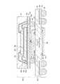
図6は、本発明の第5実施形態に係る半導体装置の構成を示す断面図である。なお、この第5実施形態は、半導体チップ103a、103bが両面にフリップチップ実装されたキャリア基板101上に、スタックド構造の半導体チップ113a〜113cを3次元実装するようにしたものである。
【0057】
図6において、半導体パッケージPK41にはキャリア基板101が設けられ、キャリア基板101の両面にはランド102a、102cがそれぞれ形成されるとともに、キャリア基板101内には内部配線102bが形成されている。そして、キャリア基板101の両面には、半導体チップ103a、103bがそれぞれフリップチップ実装され、半導体チップ103a、103bには、フリップチップ実装するための突出電極104a、104bがそれぞれ設けられている。そして、半導体チップ103a、103bにそれぞれ設けられた突出電極104a、104bは、異方性導電シート105a、105bをそれぞれ介してランド102c、102a上にそれぞれACF接合されている。なお、半導体チップ103a、103bをキャリア基板101上に実装する場合、ACF接合を用いる方法以外にも、例えば、NCF接合などのその他の接着剤接合を用いるようにしてもよく、半田接合や合金接合などの金属接合を用いるようにしてもよい。また、キャリア基板101の裏面に設けられたランド102a上には、キャリア基板101をマザー基板上に実装するための突出電極106が設けられている。ここで、キャリア基板101の表裏に半導体チップ103a、103bをそれぞれ搭載することにより、キャリア基板101の表裏における線膨張係数の差異を低減することが可能となり、キャリア基板101の反りを低減することが可能となる。
【0058】
一方、半導体パッケージPK42にはキャリア基板111が設けられ、キャリア基板111の両面にはランド112a、112cがそれぞれ形成されるとともに、キャリア基板111内には内部配線112bが形成されている。
また、半導体チップ113a〜113cには、電極パッド114a〜114cがそれぞれ設けられるとともに、各電極パッド114a〜114cが露出するようにして、絶縁膜115a〜115cがそれぞれ設けられている。そして、半導体チップ113a〜113cには、例えば、各電極パッド114a〜114cの位置に対応して、貫通孔116a〜116cがそれぞれ形成され、貫通孔116a〜116c内には、絶縁膜117a〜117cおよび導電膜118a〜118cをそれぞれ介して、貫通電極119a〜119cがそれぞれ形成されている。そして、貫通電極119a〜119cが形成された半導体チップ113a〜113cは、貫通電極119a〜119cをそれぞれ介して積層され、半導体チップ113a〜113c間の隙間には樹脂120a、120bがそれぞれ注入されている。
【0059】
また、半導体チップ113aに形成された貫通電極119a上には、半導体チップ113a〜113cの積層構造をフリップチップ実装するための突出電極121が設けられている。そして、キャリア基板111上に設けられたランド112c上に突出電極121が接合されるとともに、キャリア基板111上に実装された半導体チップ113aの表面が封止樹脂122で封止され、半導体チップ113a〜113cの積層構造がキャリア基板111上に実装されている。
【0060】
また、キャリア基板111の裏面に設けられたランド112a上には、キャリア基板111が半導体チップ103a上に保持されるように、キャリア基板111をキャリア基板101上に実装するための突出電極123が設けられている。
ここで、突出電極123は、半導体チップ103aの搭載領域を避けるようにして配置され、例えば、キャリア基板111の周囲に突出電極123を配置することができる。そして、キャリア基板101上に設けられたランド102c上に突出電極123を接合させることにより、キャリア基板111をキャリア基板101上に実装することができる。
【0061】
これにより、キャリア基板101の反りを抑制しつつ、半導体チップ111a〜111cの積層構造を半導体チップ103a上に実装することが可能となる。このため、キャリア基板101、111間の接続信頼性を確保しつつ、異種パッケージPK41、PK42を積層することが可能となり、積層時の高さの増大を抑制しつつ、異種の半導体チップ103a、103b、113a〜113cの3次元実装構造を実現することが可能となる。
【0062】
なお、突出電極104a104b、106、121、123としては、例えば、Auバンプ、半田材などで被覆されたCuバンプやNiバンプ、あるいは半田ボールなどを用いることができる。また、上述した実施形態では、半導体チップ113a〜113cの3層構造をキャリア基板111上に実装する方法について説明したが、キャリア基板111上に実装される半導体チップの積層構造は、2層または4層以上であってもよい。
【0063】
図7は、本発明の第6実施形態に係る半導体装置の構成を示す断面図である。なお、この第6実施形態は、半導体チップ203a、203bが両面にフリップチップ実装されたキャリア基板201上に、W−CSP(ウエハレベル−チップサイズパッケージ)を3次元実装するようにしたものである。
図7において、半導体パッケージPK51にはキャリア基板201が設けられ、キャリア基板201の両面にはランド202a、202cがそれぞれ形成されるとともに、キャリア基板201内には内部配線202bが形成されている。そして、キャリア基板201の両面には、半導体チップ203a、203bがそれぞれフリップチップ実装され、半導体チップ203a、203bには、フリップチップ実装するための突出電極204a、204bがそれぞれ設けられている。そして、半導体チップ203a、203bにそれぞれ設けられた突出電極204a、204bは、異方性導電シート205a、205bをそれぞれ介してランド202c、202a上にそれぞれACF接合されている。また、キャリア基板201の裏面に設けられたランド202a上には、キャリア基板201をマザー基板上に実装するための突出電極206が設けられている。ここで、キャリア基板201の表裏に半導体チップ203a、203bをそれぞれ搭載することにより、キャリア基板201の表裏における線膨張係数の差異を低減することが可能となり、キャリア基板201の反りを低減することが可能となる。
【0064】
一方、半導体パッケージPK52には半導体チップ211が設けられ、半導体チップ211には、電極パッド212が設けられるとともに、電極パッド212が露出するようにして、絶縁膜213が設けられている。そして、半導体チップ211上には、電極パッド212が露出するようにして応力緩和層214が形成され、電極パッド212上には、応力緩和層214上に延伸された再配置配線215が形成されている。そして、再配置配線215上にはソルダレジスト膜216が形成され、ソルダレジスト膜216には、応力緩和層214上において再配置配線215を露出させる開口部217が形成されている。そして、開口部217を介して露出された再配置配線215上には、半導体パッケージPK52が半導体チップ203a上に保持されるように、半導体チップ211をキャリア基板201上にフェースダウン実装するための突出電極218が設けられている。
【0065】
ここで、突出電極218は、半導体チップ203aの搭載領域を避けるようにして配置され、例えば、半導体チップ211の周囲に突出電極218を配置することができる。そして、キャリア基板201上に設けられたランド202c上に突出電極218を接合することにより、半導体パッケージPK52をキャリア基板201上に実装することができる。
【0066】
これにより、キャリア基板201の反りを抑制しつつ、半導体チップ203a、203bが両面にフリップチップ実装されたキャリア基板201上にW−CSPを積層することができる。このため、半導体チップ203a、203b、211の種類またはサイズが異なる場合においても、半導体チップ203、211間にキャリア基板を介在させることなく、半導体チップ203上に半導体チップ211を3次元実装することが可能となるとともに、キャリア基板201、211間の接続信頼性を向上させることが可能となり、3次元実装された半導体チップ203a、203b、211の信頼性の劣化を抑制しつつ、半導体チップ203a、203b、211実装時の省スペース化を図ることが可能となる。
【0067】
なお、半導体パッケージPK52をキャリア基板201上に実装する場合、例えば、ACF接合やNCF接合などの接着剤接合を用いるようにしてもよく、半田接合や合金接合などの金属接合を用いるようにしてもよい。また、突出電極204a、204b、206、218としては、例えば、Auバンプ、半田材などで被覆されたCuバンプやNiバンプ、あるいは半田ボールなどを用いることができる。また、上述した実施形態では、キャリア基板201上にフリップチップ実装された1個の半導体チップ203a上に半導体パッケージPK52を実装する方法を例にとって説明したが、キャリア基板201上にフリップチップ実装された複数の半導体チップ上に半導体パッケージPK52を実装するようにしてもよい。
【0068】
図8は、本発明の第7実施形態に係る半導体装置の構成を示す断面図である。なお、この第7実施形態は、半導体チップ323がACF接合により実装された半導体パッケージPK61上に、スタックド構造の半導体チップ333a、333bが表面に実装されるとともに、半導体チップ333cが裏面に実装された半導体パッケージPK62を積層したものである。
【0069】
図8において、半導体パッケージPK61にはキャリア基板321が設けられ、キャリア基板321の両面にはランド322a、322cがそれぞれ形成されるとともに、キャリア基板321内には内部配線322bが形成されている。そして、キャリア基板321の裏面には、半導体チップ323がフリップチップ実装され、半導体チップ323には、フリップチップ実装するための突出電極324が設けられている。そして、半導体チップ323に設けられた突出電極324は、異方性導電シート325を介してランド322a上にACF接合されている。また、キャリア基板321の裏面に設けられたランド322a上には、キャリア基板321をマザー基板上に実装するための突出電極326が設けられている。
【0070】
ここで、ACF接合により半導体チップ323をキャリア基板321に実装することにより、ワイヤボンドやモールド封止するためのスペースが不要となり、3次元実装時の省スペース化を図ることが可能となるとともに、半導体チップ323をキャリア基板321上に接合する際の低温化を図ることが可能となり、実際の使用時のキャリア基板321の反りを低減することが可能となる。
【0071】
一方、半導体パッケージPK62にはキャリア基板331が設けられ、キャリア基板331の両面にはランド332a、332cがそれぞれ形成されるとともに、キャリア基板331内には内部配線332bが形成されている。そして、キャリア基板331上には、接着層334aを介し半導体チップ333aがフェースアップ実装され、半導体チップ333は、導電性ワイヤ335aを介してランド332cにワイヤボンド接続されている。さらに、半導体チップ333a上には、導電性ワイヤ335aを避けるようにして、半導体チップ333bがフェースアップ実装され、半導体チップ333bは、接着層334bを介して半導体チップ333a上に固定されるとともに、導電性ワイヤ335bを介してランド332cにワイヤボンド接続されている。
【0072】
また、キャリア基板331の裏面には、半導体チップ333cがフリップチップ実装され、半導体チップ333cには、フリップチップ実装するための突出電極334cが設けられている。そして、半導体チップ333cに設けられた突出電極334cは、異方性導電シート335cを介してランド332a上にACF接合されている。さらに、キャリア基板331の裏面に設けられたランド332a上には、キャリア基板331をキャリア基板321上に実装するための突出電極336が設けられている。そして、キャリア基板321上に設けられたランド322cに突出電極336を接合させることにより、キャリア基板31をキャリア基板321上に実装することができる。
【0073】
ここで、キャリア基板331の表面に半導体チップ333a、333bを搭載するとともに、キャリア基板331の裏面に半導体チップ333cを搭載することにより、キャリア基板331の表裏における線膨張係数の差異を低減することが可能となり、キャリア基板331の反りを低減することが可能となる。
このため、キャリア基板331の反りを抑制しつつ、パッケージングの異なる半導体チップ333a〜333cを半導体チップ323上に積層することが可能となる。この結果、キャリア基板321、331間の接続信頼性を確保しつつ、異種パッケージPK61、PK62を積層することが可能となり、異種の半導体チップ323、333a〜333cの3次元実装構造を実現することが可能となる。
【0074】
また、半導体チップ333a、333bは封止樹脂337により封止され、封止樹脂337は、例えば、エポキシ樹脂などの熱硬化性樹脂を用いたモールド成形などにより形成することができる。
なお、上述した実施形態では、キャリア基板の両面に半導体チップを搭載する方法について説明したが、キャリア基板の一方の面に半導体チップを搭載し、キャリア基板の他方の面にダミーチップを搭載するようにしてもよい。これにより、ダミーチップとして、半導体系材料のほか、金属系材料、セラミック系材料または樹脂系材料などを使用することができ、キャリア基板に搭載可能な材料に制約をなくすことが可能となることから、キャリア基板の反りの状態を精密に制御することが可能となる。
【0075】
また、上述した半導体装置および電子デバイスは、例えば、液晶表示装置、携帯電話、携帯情報端末、ビデオカメラ、デジタルカメラ、MD(Mini Disc)プレーヤなどの電子機器に適用することができ、電子機器の小型・軽量化を可能としつつ、電子機器の信頼性を向上させることができる。
また、上述した実施形態では、半導体チップまたは半導体パッケージを実装する方法を例にとって説明したが、本発明は、必ずしも半導体チップまたは半導体パッケージを実装する方法に限定されることなく、例えば、弾性表面波(SAW)素子などのセラミック素子、光変調器や光スイッチなどの光学素子、磁気センサやバイオセンサなどの各種センサ類などを実装するようにしてもよい。
【図面の簡単な説明】
【図1】 第1実施形態に係る半導体装置の構成を示す断面図。
【図2】 第2実施形態に係る半導体装置の構成を示す断面図。
【図3】 第3実施形態に係る半導体装置の構成を示す断面図。
【図4】 第4実施形態に係る半導体装置の製造方法を示す断面図。
【図5】 第4実施形態に係る半導体装置の製造方法を示す断面図。
【図6】 第5実施形態に係る半導体装置の製造方法を示す断面図。
【図7】 第6実施形態に係る半導体装置の構成を示す断面図。
【図8】 第7実施形態に係る半導体装置の構成を示す断面図。
【符号の説明】
21、31、41、51、61、61a〜61c、71、81、101、111、201、321、331 キャリア基板、22a、22c、32a、32c、42a、42c、52a、52c、72a、72b、82、102a、102c、112a、112c、202a、202c、322a、322c、332a、332c ランド、22b、32b、42b、52b、102b、112b、202b、322b、332b 内部配線、23a、23b、33a、33b、43a、43b、53a、53b、62a〜62c、73a、73b、103a、103b、113a〜113c、203a、203b、211、323、333a〜333c 半導体チップ、24a、24b、26、36、44a、44b、46、55a、56、65a〜65c、74a、74b、77、83、104a、104b、121、123、204a、204b、206、218、324、326、334c、336 突出電極、25a、25b、45a、45b、54a、75a、75b、105a、105b、205a、205b、325、335c 異方性導電シート、34a、34b、54b、334a、334b 接着層、35a、35b、55b、63a〜63c、335a、335b 導電性ワイヤ、37、57、64、64a〜64c、84、120a、120b、122、337 封止樹脂、76 フラックス、78 セパレータ、114a〜114c、212 電極パッド、115a〜115c、117a〜117c、213絶縁膜、116a〜116c 貫通孔、118a〜118c 導電膜、119a〜119c 貫通電極、214 応力緩和層、215 再配置配線、216 ソルダレジスト層、217 開口部、PK11、PK12、PK21、PK22、PK31、PK32、PK41、PK42、PK51、PK52、PK61、PK62 半導体パッケージ[0001]
BACKGROUND OF THE INVENTION
The present invention relates to a semiconductor device, an electronic device, an electronic device, a method for manufacturing a semiconductor device, and a method for manufacturing an electronic device, and is particularly suitable for application to a laminated structure such as a semiconductor package.
[0002]
[Prior art]
In a conventional semiconductor device, there is a method of three-dimensionally mounting a semiconductor chip via a carrier substrate, for example, as disclosed in Patent Document 1 in order to save space when mounting a semiconductor chip.
[0003]
[Patent Document 1]
Japanese Patent Laid-Open No. 10-284683
[0004]
[Problems to be solved by the invention]
However, the method of three-dimensionally mounting a semiconductor chip via a carrier substrate has a problem that the warpage of the carrier substrate increases because the linear expansion coefficient differs between the front and back surfaces of the carrier substrate.
SUMMARY OF THE INVENTION An object of the present invention is to provide a semiconductor device and a method for manufacturing the semiconductor device that can realize a three-dimensional mounting structure of different types of chips while suppressing warping of a carrier substrate.
[0005]
[Means for Solving the Problems]
In order to solve the above-described problem, according to a semiconductor device of one embodiment of the present invention, a first carrier substrate, a first semiconductor chip mounted face-down on the first carrier substrate, and the first carrier A second semiconductor chip face-down mounted on the back surface of the substrate, a second carrier substrate, a third semiconductor chip mounted on the second carrier substrate, and the second carrier substrate on the first semiconductor chip The second carrier substrate, comprising: a protruding electrode that connects the second carrier substrate and the first carrier substrate and a sealing material made of a mold resin that seals the third semiconductor chip so as to be held. Is fixed on the first carrier substrate so as to straddle the first semiconductor chip, and the side wall of the sealing material coincides with the position of the side wall of the second carrier substrate. .
[0006]
As a result, semiconductor chips having the same material properties can be provided on the front and back sides of the first carrier substrate, and the difference in coefficient of linear expansion between the front and back sides of the first carrier substrate can be reduced. For this reason, it becomes possible to laminate | stack a 2nd carrier board | substrate on a 1st carrier board | substrate, suppressing the curvature of a 1st carrier board | substrate, ensuring the connection reliability of a 1st carrier board | substrate and a 2nd carrier board | substrate. It becomes possible to realize a three-dimensional mounting structure of different types of chips.
In addition, by matching the side wall of the sealing material with the position of the side wall of the second carrier substrate, the third semiconductor chip is suppressed while suppressing an increase in height when the second carrier substrate is stacked on the first carrier substrate. The entire surface of the second carrier substrate can be reinforced with the sealing material that seals the third semiconductor chip, and the third semiconductor chip can be sealed without dividing the sealing material into cells. It becomes possible to increase the mounting area of the third semiconductor chip mounted on the two-carrier substrate.
[0011]
The semiconductor device according to one aspect of the present invention is characterized in that the first semiconductor chip and the second semiconductor chip are connected to the first carrier substrate by pressure welding.
Accordingly, it is possible to reduce the temperature when the first semiconductor chip and the second semiconductor chip are connected to the first carrier substrate, and it is possible to reduce the warp of the first carrier substrate during actual use. Become.
[0012]
Further, according to the semiconductor device of one embodiment of the present invention, the semiconductor device including the first carrier substrate and the semiconductor device including the second carrier substrate have different elastic moduli at the same temperature.
Accordingly, it is possible to suppress warpage generated in one carrier substrate with the other carrier substrate, and it is possible to improve connection reliability between the first carrier substrate and the second carrier substrate.
[0013]
Also, according to the semiconductor device of one aspect of the present invention, the first carrier substrate on which the first semiconductor chip and the second semiconductor chip are mounted is a flip-chip mounted ball grid array, and the third semiconductor chip is The mounted second carrier substrate is a ball grid array or chip size package that is sealed with a mold.
[0014]
This makes it possible to stack different types of packages while suppressing an increase in the height of the three-dimensional mounting structure, and it is possible to save space when mounting semiconductor chips even when the types of semiconductor chips are different It becomes.
In the semiconductor device according to one aspect of the present invention, the third semiconductor chip includes a structure in which a plurality of chips are stacked.
[0015]
As a result, a plurality of third semiconductor chips of different types or sizes can be stacked on the first semiconductor chip, and various functions can be provided while saving space when mounting the semiconductor chip. Is possible.
In the semiconductor device according to one aspect of the present invention, the third semiconductor chip includes a structure in which a plurality of chips are arranged in parallel on the second carrier substrate.
[0016]
As a result, it is possible to stack a plurality of third semiconductor chips on the first semiconductor chip while suppressing an increase in height when the third semiconductor chip is stacked, and deterioration in connection reliability during three-dimensional mounting. Thus, it is possible to save space when mounting the semiconductor chip.
[0022]
In addition, according to the method for manufacturing a semiconductor device of one embodiment of the present invention, the step of mounting the first semiconductor chip on the first carrier substrate face down, and the second semiconductor chip on the back surface of the first carrier substrate. A step of down-mounting, a step of mounting a third semiconductor chip on the second carrier substrate, a step of forming a protruding electrode on the second carrier substrate, and a third semiconductor chip mounted on the second carrier substrate And connecting the second carrier substrate and the first carrier substrate via the protruding electrode so that the second carrier substrate is held on the first semiconductor chip. A step of sealing the third semiconductor chip with the sealing resin, wherein the plurality of third semiconductor chips mounted on the second carrier substrate are integrally molded with the sealing resin. A step of shape, characterized in that it comprises a step of cutting the second carrier substrate is molded by the sealing resin for each of the third semiconductor chip.
[0023]
Thus, the second carrier substrate can be stacked on the first carrier substrate with the first and second semiconductor chips provided on the front and back surfaces of the first carrier substrate. Therefore, it is possible to stack the third semiconductor chips with different packaging on the first semiconductor chip while suppressing the warp of the first carrier substrate. It is possible to realize the three-dimensional mounting structure.
Further, the third semiconductor chip can be sealed with the sealing resin without dividing the sealing resin into cells for each third semiconductor chip, and the entire surface of the second carrier substrate can be sealed with the sealing resin. It becomes possible to reinforce with.
For this reason, even when the type or size of the third semiconductor chip is different, it is possible to share a mold at the time of molding, to improve the efficiency of the sealing resin process, and to divide the cells. Therefore, it is possible to increase the mounting area of the third semiconductor chip mounted on the second carrier substrate.
[0028]
DETAILED DESCRIPTION OF THE INVENTION
Hereinafter, semiconductor devices, electronic devices, and manufacturing methods thereof according to embodiments of the present invention will be described with reference to the drawings.
FIG. 1 is a cross-sectional view showing the configuration of the semiconductor device according to the first embodiment of the present invention. In the first embodiment, the semiconductor chips (or semiconductor dies) 33a and 33b having a stacked structure are connected by wire bonding on the semiconductor package PK11 in which the semiconductor chips (or semiconductor dies) 23a and 23b are mounted on both sides by ACF bonding. The stacked semiconductor packages PK12 are stacked.
[0029]
In FIG. 1, a semiconductor substrate PK11 is provided with a
[0030]
Here, by mounting the semiconductor chips 23 a and 23 b on the front and back of the
[0031]
The thickness and size of the
On the other hand, a
[0032]
On the
[0033]
Thereby, it is possible to stack the
[0034]
Further, the
Here, various types of
[0035]
As the
[0036]
In the above-described embodiment, the method of mounting the semiconductor chip 23 on the
[0037]
FIG. 2 is a cross-sectional view showing a configuration of a semiconductor device according to the second embodiment of the present invention. In the second embodiment, a semiconductor package PK22 in which
[0038]
In FIG. 2, a
[0039]
Here, by mounting the
[0040]
On the other hand, a
[0041]
Here, by mounting the
[0042]
On the
[0043]
This makes it possible to stack the semiconductor chips 53 a and 53 b with different packaging on the semiconductor chip 43 while suppressing the warp of the
[0044]
As the protruding
Further, the
[0045]
Here, various types of
[0046]
FIG. 3 is a cross-sectional view illustrating a method for manufacturing a semiconductor device according to a third embodiment of the present invention. In the third embodiment, after the plurality of
[0047]
In FIG. 3A, the
[0048]
Next, as shown in FIG. 3B, the plurality of
[0049]
Next, as shown in FIG. 3C, protruding
[0050]
Here, by cutting the
[0051]
4 and 5 are cross-sectional views illustrating a method of manufacturing a semiconductor device according to the fourth embodiment of the present invention. In the fourth embodiment, a semiconductor package PK32 sealed with a sealing
4A, a
[0052]
Next, as shown in FIG. 4B, the
[0053]
When the
[0054]
Next, in FIG. 5A, a semiconductor substrate PK32 is provided with a
[0055]
When the semiconductor package PK32 is stacked on the semiconductor package PK31, the
Next, as shown in FIG. 5B, the semiconductor package PK32 is mounted on the semiconductor package PK31, and a reflow process is performed to bond the protruding
[0056]
Next, as shown in FIG. 5C, the protruding
FIG. 6 is a cross-sectional view showing a configuration of a semiconductor device according to the fifth embodiment of the present invention. In the fifth embodiment,
[0057]
In FIG. 6, a
[0058]
On the other hand, a
The
[0059]
Further, on the through
[0060]
A protruding
Here, the protruding
[0061]
As a result, the stacked structure of the semiconductor chips 111a to 111c can be mounted on the
[0062]
As the protruding electrodes 104a104b, 106, 121, 123, for example, Au bumps, Cu bumps coated with a solder material, Ni bumps, solder balls, or the like can be used. In the above-described embodiment, the method of mounting the three-layer structure of the
[0063]
FIG. 7 is a sectional view showing a configuration of a semiconductor device according to the sixth embodiment of the present invention. In the sixth embodiment, W-CSP (wafer level-chip size package) is three-dimensionally mounted on a
In FIG. 7, a
[0064]
On the other hand, the semiconductor package PK52 is provided with a
[0065]
Here, the protruding
[0066]
Thereby, W-CSP can be laminated | stacked on the
[0067]
When the semiconductor package PK52 is mounted on the
[0068]
FIG. 8 is a cross-sectional view showing a configuration of a semiconductor device according to the seventh embodiment of the present invention. In the seventh embodiment, stacked
[0069]
In FIG. 8, a semiconductor substrate PK61 is provided with a
[0070]
Here, by mounting the
[0071]
On the other hand, a
[0072]
A
[0073]
Here, by mounting the
For this reason, it is possible to stack the
[0074]
The
In the above-described embodiment, the method of mounting the semiconductor chip on both surfaces of the carrier substrate has been described. However, the semiconductor chip is mounted on one surface of the carrier substrate and the dummy chip is mounted on the other surface of the carrier substrate. It may be. As a result, in addition to semiconductor materials, metal materials, ceramic materials, or resin materials can be used as dummy chips, and it is possible to eliminate restrictions on materials that can be mounted on the carrier substrate. It becomes possible to precisely control the state of warping of the carrier substrate.
[0075]
The above-described semiconductor device and electronic device can be applied to electronic devices such as a liquid crystal display device, a mobile phone, a portable information terminal, a video camera, a digital camera, and an MD (Mini Disc) player. The reliability of the electronic device can be improved while enabling reduction in size and weight.
In the above-described embodiments, the method for mounting the semiconductor chip or the semiconductor package has been described as an example. However, the present invention is not necessarily limited to the method for mounting the semiconductor chip or the semiconductor package. Ceramic elements such as (SAW) elements, optical elements such as light modulators and optical switches, various sensors such as magnetic sensors and biosensors, and the like may be mounted.
[Brief description of the drawings]
FIG. 1 is a cross-sectional view showing a configuration of a semiconductor device according to a first embodiment.
FIG. 2 is a cross-sectional view showing a configuration of a semiconductor device according to a second embodiment.
FIG. 3 is a cross-sectional view showing a configuration of a semiconductor device according to a third embodiment.
FIG. 4 is a cross-sectional view showing a method for manufacturing a semiconductor device according to a fourth embodiment.
FIG. 5 is a cross-sectional view showing a method for manufacturing a semiconductor device according to a fourth embodiment.
FIG. 6 is a cross-sectional view showing a method for manufacturing a semiconductor device according to a fifth embodiment.
FIG. 7 is a cross-sectional view showing a configuration of a semiconductor device according to a sixth embodiment.
FIG. 8 is a cross-sectional view showing a configuration of a semiconductor device according to a seventh embodiment.
[Explanation of symbols]
21, 31, 41, 51, 61, 61a-61c, 71, 81, 101, 111, 201, 321, 331 Carrier substrate, 22a, 22c, 32a, 32c, 42a, 42c, 52a, 52c, 72a, 72b, 82, 102a, 102c, 112a, 112c, 202a, 202c, 322a, 322c, 332a, 332c Land, 22b, 32b, 42b, 52b, 102b, 112b, 202b, 322b, 332b Internal wiring, 23a, 23b, 33a, 33b 43a, 43b, 53a, 53b, 62a-62c, 73a, 73b, 103a, 103b, 113a-113c, 203a, 203b, 211, 323, 333a-333c Semiconductor chip, 24a, 24b, 26, 36, 44a, 44b 46, 55a, 56, 65 a to 65c, 74a, 74b, 77, 83, 104a, 104b, 121, 123, 204a, 204b, 206, 218, 324, 326, 334c, 336 Projecting electrode, 25a, 25b, 45a, 45b, 54a, 75a, 75b, 105a, 105b, 205a, 205b, 325, 335c Anisotropic conductive sheet, 34a, 34b, 54b, 334a, 334b Adhesive layer, 35a, 35b, 55b, 63a-63c, 335a, 335b Conductive wire, 37, 57, 64, 64a to 64c, 84, 120a, 120b, 122, 337 Sealing resin, 76 flux, 78 separator, 114a to 114c, 212 electrode pad, 115a to 115c, 117a to 117c, 213 insulating film, 116a to 116c Through hole, 118a-118c Electrode film, 119a to 119c through electrode, 214 stress relaxation layer, 215 rearrangement wiring, 216 solder resist layer, 217 opening, PK11, PK12, PK21, PK22, PK31, PK32, PK41, PK42, PK51, PK52, PK61, PK62 semiconductor package
Claims (7)
Translated fromJapanese前記第1キャリア基板上にフェースダウン実装された第1半導体チップと、
前記第1キャリア基板の裏面にフェースダウン実装された第2半導体チップと、
第2キャリア基板と、
前記第2キャリア基板上に搭載された第3半導体チップと、
前記第2キャリア基板が前記第1半導体チップ上に保持されるように、前記第2キャリア基板と前記第1キャリア基板とを接続する突出電極と、
前記第3半導体チップを封止するモールド樹脂からなる封止材とを備え、
前記第2キャリア基板は前記第1半導体チップ上に跨るように、第1キャリア基板上に固定され、
前記封止材の側壁は前記第2キャリア基板の側壁の位置に一致していることを特徴とする半導体装置。A first carrier substrate;
A first semiconductor chip facedown mounted on the first carrier substrate;
A second semiconductor chip facedown mounted on the back surface of the first carrier substrate;
A second carrier substrate;
A third semiconductor chip mounted on the second carrier substrate;
A protruding electrode connecting the second carrier substrate and the first carrier substrate so that the second carrier substrate is held on the first semiconductor chip;
And a sealing material made of mold resin for sealing the third semiconductor chip,
The second carrier substrate is fixed on the first carrier substrate so as to straddle the first semiconductor chip,
The semiconductor device according to claim 1, wherein a side wall of the sealing material coincides with a position of a side wall of the second carrier substrate.
第2半導体チップを前記第1キャリア基板の裏面にフェースダウン実装する工程と、
第3半導体チップを第2キャリア基板上に実装する工程と、
前記第2キャリア基板に突出電極を形成する工程と、
前記第2キャリア基板上に実装された第3半導体チップを封止樹脂で封止する工程と、
前記第2キャリア基板が前記第1半導体チップ上に保持されるように、前記突出電極を介して前記第2キャリア基板と前記第1キャリア基板とを接続する工程とを備え、
前記第3半導体チップを前記封止樹脂で封止する工程は、
前記第2キャリア基板に実装された複数の第3半導体チップを封止樹脂で一体的にモールド成形する工程と、
前記封止樹脂によりモールド成形された前記第2キャリア基板を前記第3半導体チップごとに切断する工程とを備えることを特徴とする半導体装置の製造方法。Mounting a first semiconductor chip face down on a first carrier substrate;
Mounting a second semiconductor chip facedown on the back surface of the first carrier substrate;
Mounting the third semiconductor chip on the second carrier substrate;
Forming a protruding electrode on the second carrier substrate;
Sealing a third semiconductor chip mounted on the second carrier substrate with a sealing resin;
Connecting the second carrier substrate and the first carrier substrate via the protruding electrode so that the second carrier substrate is held on the first semiconductor chip,
Sealing the third semiconductor chip with the sealing resin,
A step of integrally molding a plurality of third semiconductor chips mounted on the second carrier substrate with a sealing resin;
And a step of cutting the second carrier substrate molded by the sealing resin for each third semiconductor chip.
Priority Applications (3)
| Application Number | Priority Date | Filing Date | Title |
|---|---|---|---|
| JP2003074220AJP3680839B2 (en) | 2003-03-18 | 2003-03-18 | Semiconductor device and manufacturing method of semiconductor device |
| US10/801,933US20040222508A1 (en) | 2003-03-18 | 2004-03-16 | Semiconductor device, electronic device, electronic apparatus, method of manufacturing semiconductor device, and method of manufacturing electronic device |
| CNB2004100397309ACN100342538C (en) | 2003-03-18 | 2004-03-16 | Semiconductor device, electronic apparatus and their manufacturing methods, electronic equipment |
Applications Claiming Priority (1)
| Application Number | Priority Date | Filing Date | Title |
|---|---|---|---|
| JP2003074220AJP3680839B2 (en) | 2003-03-18 | 2003-03-18 | Semiconductor device and manufacturing method of semiconductor device |
Publications (2)
| Publication Number | Publication Date |
|---|---|
| JP2004281921A JP2004281921A (en) | 2004-10-07 |
| JP3680839B2true JP3680839B2 (en) | 2005-08-10 |
Family
ID=33289924
Family Applications (1)
| Application Number | Title | Priority Date | Filing Date |
|---|---|---|---|
| JP2003074220AExpired - Fee RelatedJP3680839B2 (en) | 2003-03-18 | 2003-03-18 | Semiconductor device and manufacturing method of semiconductor device |
Country Status (3)
| Country | Link |
|---|---|
| US (1) | US20040222508A1 (en) |
| JP (1) | JP3680839B2 (en) |
| CN (1) | CN100342538C (en) |
Cited By (1)
| Publication number | Priority date | Publication date | Assignee | Title |
|---|---|---|---|---|
| KR101784354B1 (en) | 2016-03-11 | 2017-10-12 | 서울과학기술대학교 산학협력단 | Mesh-type stretchable packaging apparatus |
Families Citing this family (50)
| Publication number | Priority date | Publication date | Assignee | Title |
|---|---|---|---|---|
| TW200504895A (en)* | 2003-06-04 | 2005-02-01 | Renesas Tech Corp | Semiconductor device |
| JP4269806B2 (en)* | 2003-06-30 | 2009-05-27 | カシオ計算機株式会社 | Semiconductor device and manufacturing method thereof |
| TWI283467B (en)* | 2003-12-31 | 2007-07-01 | Advanced Semiconductor Eng | Multi-chip package structure |
| JP4353845B2 (en)* | 2004-03-31 | 2009-10-28 | 富士通株式会社 | Manufacturing method of semiconductor device |
| CN100373614C (en)* | 2004-11-08 | 2008-03-05 | 日月光半导体制造股份有限公司 | Multi-chip packaging structure |
| JP2007123501A (en)* | 2005-10-27 | 2007-05-17 | Alps Electric Co Ltd | Forming method of solder terminal |
| JP4512545B2 (en) | 2005-10-27 | 2010-07-28 | パナソニック株式会社 | Multilayer semiconductor module |
| US7462509B2 (en)* | 2006-05-16 | 2008-12-09 | International Business Machines Corporation | Dual-sided chip attached modules |
| US7829438B2 (en) | 2006-10-10 | 2010-11-09 | Tessera, Inc. | Edge connect wafer level stacking |
| US7901989B2 (en) | 2006-10-10 | 2011-03-08 | Tessera, Inc. | Reconstituted wafer level stacking |
| US8513789B2 (en) | 2006-10-10 | 2013-08-20 | Tessera, Inc. | Edge connect wafer level stacking with leads extending along edges |
| US8569876B2 (en) | 2006-11-22 | 2013-10-29 | Tessera, Inc. | Packaged semiconductor chips with array |
| US7791199B2 (en)* | 2006-11-22 | 2010-09-07 | Tessera, Inc. | Packaged semiconductor chips |
| US7952195B2 (en)* | 2006-12-28 | 2011-05-31 | Tessera, Inc. | Stacked packages with bridging traces |
| US8405196B2 (en)* | 2007-03-05 | 2013-03-26 | DigitalOptics Corporation Europe Limited | Chips having rear contacts connected by through vias to front contacts |
| US7994643B2 (en)* | 2007-04-04 | 2011-08-09 | Samsung Electronics Co., Ltd. | Stack package, a method of manufacturing the stack package, and a digital device having the stack package |
| JP4864810B2 (en)* | 2007-05-21 | 2012-02-01 | 新光電気工業株式会社 | Manufacturing method of chip embedded substrate |
| JP5572089B2 (en) | 2007-07-27 | 2014-08-13 | テッセラ,インコーポレイテッド | Reconfigured wafer stack packaging with pad extension after application |
| WO2009017835A2 (en)* | 2007-07-31 | 2009-02-05 | Tessera, Inc. | Semiconductor packaging process using through silicon vias |
| US8551815B2 (en)* | 2007-08-03 | 2013-10-08 | Tessera, Inc. | Stack packages using reconstituted wafers |
| US8043895B2 (en)* | 2007-08-09 | 2011-10-25 | Tessera, Inc. | Method of fabricating stacked assembly including plurality of stacked microelectronic elements |
| US20100053407A1 (en)* | 2008-02-26 | 2010-03-04 | Tessera, Inc. | Wafer level compliant packages for rear-face illuminated solid state image sensors |
| US20090212381A1 (en)* | 2008-02-26 | 2009-08-27 | Tessera, Inc. | Wafer level packages for rear-face illuminated solid state image sensors |
| JP5639052B2 (en) | 2008-06-16 | 2014-12-10 | テッセラ,インコーポレイテッド | Edge stacking at wafer level |
| US20170117214A1 (en) | 2009-01-05 | 2017-04-27 | Amkor Technology, Inc. | Semiconductor device with through-mold via |
| WO2010104610A2 (en) | 2009-03-13 | 2010-09-16 | Tessera Technologies Hungary Kft. | Stacked microelectronic assemblies having vias extending through bond pads |
| US8791575B2 (en) | 2010-07-23 | 2014-07-29 | Tessera, Inc. | Microelectronic elements having metallic pads overlying vias |
| US9640437B2 (en) | 2010-07-23 | 2017-05-02 | Tessera, Inc. | Methods of forming semiconductor elements using micro-abrasive particle stream |
| US8796135B2 (en) | 2010-07-23 | 2014-08-05 | Tessera, Inc. | Microelectronic elements with rear contacts connected with via first or via middle structures |
| US8847376B2 (en)* | 2010-07-23 | 2014-09-30 | Tessera, Inc. | Microelectronic elements with post-assembly planarization |
| US8847380B2 (en) | 2010-09-17 | 2014-09-30 | Tessera, Inc. | Staged via formation from both sides of chip |
| US8610259B2 (en) | 2010-09-17 | 2013-12-17 | Tessera, Inc. | Multi-function and shielded 3D interconnects |
| KR101059490B1 (en) | 2010-11-15 | 2011-08-25 | 테세라 리써치 엘엘씨 | Conductive pads constructed by embedded traces |
| US8587126B2 (en) | 2010-12-02 | 2013-11-19 | Tessera, Inc. | Stacked microelectronic assembly with TSVs formed in stages with plural active chips |
| US8736066B2 (en) | 2010-12-02 | 2014-05-27 | Tessera, Inc. | Stacked microelectronic assemby with TSVS formed in stages and carrier above chip |
| US8637968B2 (en) | 2010-12-02 | 2014-01-28 | Tessera, Inc. | Stacked microelectronic assembly having interposer connecting active chips |
| US8610264B2 (en) | 2010-12-08 | 2013-12-17 | Tessera, Inc. | Compliant interconnects in wafers |
| US8810025B2 (en)* | 2011-03-17 | 2014-08-19 | Taiwan Semiconductor Manufacturing Company, Ltd. | Reinforcement structure for flip-chip packaging |
| US9543269B2 (en)* | 2011-03-22 | 2017-01-10 | Nantong Fujitsu Microelectronics Co., Ltd. | System-level packaging methods and structures |
| WO2012126377A1 (en) | 2011-03-22 | 2012-09-27 | Nantong Fujitsu Microelectronics Co., Ltd. | System-level packaging methods and structures |
| US9414484B2 (en) | 2011-11-09 | 2016-08-09 | Intel Corporation | Thermal expansion compensators for controlling microelectronic package warpage |
| JP5865220B2 (en)* | 2012-09-24 | 2016-02-17 | ルネサスエレクトロニクス株式会社 | Semiconductor device |
| JP6252241B2 (en)* | 2014-02-27 | 2017-12-27 | セイコーエプソン株式会社 | Force detection device and robot |
| TWI552304B (en)* | 2014-04-22 | 2016-10-01 | 矽品精密工業股份有限公司 | Package on package and manufacturing method thereof |
| BR112015028568A2 (en)* | 2014-12-15 | 2017-07-25 | Intel Corp | package apparatus in inverted suspension mold package. |
| KR102495916B1 (en) | 2015-08-13 | 2023-02-03 | 삼성전자 주식회사 | Semiconductor package |
| US10460957B2 (en) | 2017-01-31 | 2019-10-29 | Skyworks Solutions, Inc. | Control of under-fill using an encapsulant for a dual-sided ball grid array package |
| KR102592327B1 (en)* | 2018-10-16 | 2023-10-20 | 삼성전자주식회사 | Semiconductor package |
| KR102739235B1 (en) | 2019-09-24 | 2024-12-05 | 삼성전자주식회사 | Semiconductor package |
| US11362027B2 (en) | 2020-02-28 | 2022-06-14 | Amkor Technology Singapore Holding Pte. Ltd. | Semiconductor devices and methods of manufacturing semiconductor devices |
Family Cites Families (19)
| Publication number | Priority date | Publication date | Assignee | Title |
|---|---|---|---|---|
| JPH08115989A (en)* | 1994-08-24 | 1996-05-07 | Fujitsu Ltd | Semiconductor device and manufacturing method thereof |
| US5994166A (en)* | 1997-03-10 | 1999-11-30 | Micron Technology, Inc. | Method of constructing stacked packages |
| JP2964983B2 (en)* | 1997-04-02 | 1999-10-18 | 日本電気株式会社 | Three-dimensional memory module and semiconductor device using the same |
| JP2000208698A (en)* | 1999-01-18 | 2000-07-28 | Toshiba Corp | Semiconductor device |
| JP3201353B2 (en)* | 1998-08-04 | 2001-08-20 | 日本電気株式会社 | Semiconductor device and manufacturing method thereof |
| US6133634A (en)* | 1998-08-05 | 2000-10-17 | Fairchild Semiconductor Corporation | High performance flip chip package |
| WO2000049656A1 (en)* | 1999-02-17 | 2000-08-24 | Hitachi, Ltd. | Semiconductor device and method of manufacture thereof |
| US6034425A (en)* | 1999-03-17 | 2000-03-07 | Chipmos Technologies Inc. | Flat multiple-chip module micro ball grid array packaging |
| US6023097A (en)* | 1999-03-17 | 2000-02-08 | Chipmos Technologies, Inc. | Stacked multiple-chip module micro ball grid array packaging |
| JP2001156212A (en)* | 1999-09-16 | 2001-06-08 | Nec Corp | Resin sealed semiconductor device and producing method therefor |
| JP3798597B2 (en)* | 1999-11-30 | 2006-07-19 | 富士通株式会社 | Semiconductor device |
| US6731009B1 (en)* | 2000-03-20 | 2004-05-04 | Cypress Semiconductor Corporation | Multi-die assembly |
| JP2001352035A (en)* | 2000-06-07 | 2001-12-21 | Sony Corp | Assembling jig for multilayer semiconductor device and manufacturing method therefor |
| US6734539B2 (en)* | 2000-12-27 | 2004-05-11 | Lucent Technologies Inc. | Stacked module package |
| JP2003218150A (en)* | 2002-01-23 | 2003-07-31 | Fujitsu Media Device Kk | Module parts |
| JP2003318361A (en)* | 2002-04-19 | 2003-11-07 | Fujitsu Ltd | Semiconductor device and method of manufacturing the same |
| US6903458B1 (en)* | 2002-06-20 | 2005-06-07 | Richard J. Nathan | Embedded carrier for an integrated circuit chip |
| JP2004179232A (en)* | 2002-11-25 | 2004-06-24 | Seiko Epson Corp | Semiconductor device, method of manufacturing the same, and electronic device |
| JP4096774B2 (en)* | 2003-03-24 | 2008-06-04 | セイコーエプソン株式会社 | SEMICONDUCTOR DEVICE, ELECTRONIC DEVICE, ELECTRONIC DEVICE, SEMICONDUCTOR DEVICE MANUFACTURING METHOD, AND ELECTRONIC DEVICE MANUFACTURING METHOD |
- 2003
- 2003-03-18JPJP2003074220Apatent/JP3680839B2/ennot_activeExpired - Fee Related
- 2004
- 2004-03-16CNCNB2004100397309Apatent/CN100342538C/ennot_activeExpired - Fee Related
- 2004-03-16USUS10/801,933patent/US20040222508A1/ennot_activeAbandoned
Cited By (1)
| Publication number | Priority date | Publication date | Assignee | Title |
|---|---|---|---|---|
| KR101784354B1 (en) | 2016-03-11 | 2017-10-12 | 서울과학기술대학교 산학협력단 | Mesh-type stretchable packaging apparatus |
Also Published As
| Publication number | Publication date |
|---|---|
| JP2004281921A (en) | 2004-10-07 |
| CN100342538C (en) | 2007-10-10 |
| CN1531090A (en) | 2004-09-22 |
| US20040222508A1 (en) | 2004-11-11 |
Similar Documents
| Publication | Publication Date | Title |
|---|---|---|
| JP3680839B2 (en) | Semiconductor device and manufacturing method of semiconductor device | |
| JP4110992B2 (en) | Semiconductor device, electronic device, electronic apparatus, semiconductor device manufacturing method, and electronic device manufacturing method | |
| US8786102B2 (en) | Semiconductor device and method of manufacturing the same | |
| JP3892259B2 (en) | Manufacturing method of semiconductor device | |
| US7309648B2 (en) | Low profile, chip-scale package and method of fabrication | |
| JP2004363126A (en) | Semiconductor device, electronic device, electronic apparatus, and method of manufacturing semiconductor device | |
| US20090127688A1 (en) | Package-on-package with improved joint reliability | |
| JP2003273317A (en) | Semiconductor device and its manufacturing method | |
| JP2004349495A (en) | Semiconductor device, electronic device, electronic apparatus, and method of manufacturing semiconductor device | |
| JP2011101044A (en) | Stacked package and method of manufacturing the same | |
| JP2003031760A (en) | Semiconductor device | |
| KR20090039411A (en) | Semiconductor package, module, system having a structure in which solder balls and chip pads are bonded, and a method of manufacturing the same | |
| JP2013045863A (en) | Semiconductor device and manufacturing method of the same | |
| JP2003078105A (en) | Stacked chip module | |
| CN101872757B (en) | Recess chip packaging structure and laminated packaging structure using same | |
| WO2013106973A1 (en) | Package-on-package semiconductor chip packaging structure and technology | |
| JP3891123B2 (en) | SEMICONDUCTOR DEVICE, ELECTRONIC DEVICE, ELECTRONIC DEVICE, AND SEMICONDUCTOR DEVICE MANUFACTURING METHOD | |
| CN100442502C (en) | Semiconductor device, electronic equipment and their manufacturing method, and electronic instrument | |
| JP3786103B2 (en) | SEMICONDUCTOR DEVICE, ELECTRONIC DEVICE, ELECTRONIC DEVICE, AND SEMICONDUCTOR DEVICE MANUFACTURING METHOD | |
| JP2004281919A (en) | Semiconductor device, electronic device, electronic equipment, method of manufacturing semiconductor device, and method of manufacturing electronic device | |
| JP4069771B2 (en) | SEMICONDUCTOR DEVICE, ELECTRONIC DEVICE, AND SEMICONDUCTOR DEVICE MANUFACTURING METHOD | |
| US8072069B2 (en) | Semiconductor device and method of manufacturing a semiconductor device | |
| KR101123799B1 (en) | Semiconductor package and method for fabricating thereof | |
| TWI442522B (en) | Cavity chip package structure and package-on-package using the same | |
| TWI387068B (en) | Cavity chip package structure and package-on-package using the same |
Legal Events
| Date | Code | Title | Description |
|---|---|---|---|
| A621 | Written request for application examination | Free format text:JAPANESE INTERMEDIATE CODE: A621 Effective date:20050105 | |
| A871 | Explanation of circumstances concerning accelerated examination | Free format text:JAPANESE INTERMEDIATE CODE: A871 Effective date:20050105 | |
| A975 | Report on accelerated examination | Free format text:JAPANESE INTERMEDIATE CODE: A971005 Effective date:20050128 | |
| A131 | Notification of reasons for refusal | Free format text:JAPANESE INTERMEDIATE CODE: A131 Effective date:20050201 | |
| A521 | Written amendment | Free format text:JAPANESE INTERMEDIATE CODE: A523 Effective date:20050404 | |
| TRDD | Decision of grant or rejection written | ||
| A01 | Written decision to grant a patent or to grant a registration (utility model) | Free format text:JAPANESE INTERMEDIATE CODE: A01 Effective date:20050426 | |
| A61 | First payment of annual fees (during grant procedure) | Free format text:JAPANESE INTERMEDIATE CODE: A61 Effective date:20050509 | |
| R150 | Certificate of patent or registration of utility model | Free format text:JAPANESE INTERMEDIATE CODE: R150 | |
| FPAY | Renewal fee payment (event date is renewal date of database) | Free format text:PAYMENT UNTIL: 20090527 Year of fee payment:4 | |
| FPAY | Renewal fee payment (event date is renewal date of database) | Free format text:PAYMENT UNTIL: 20100527 Year of fee payment:5 | |
| FPAY | Renewal fee payment (event date is renewal date of database) | Free format text:PAYMENT UNTIL: 20110527 Year of fee payment:6 | |
| FPAY | Renewal fee payment (event date is renewal date of database) | Free format text:PAYMENT UNTIL: 20120527 Year of fee payment:7 | |
| FPAY | Renewal fee payment (event date is renewal date of database) | Free format text:PAYMENT UNTIL: 20130527 Year of fee payment:8 | |
| FPAY | Renewal fee payment (event date is renewal date of database) | Free format text:PAYMENT UNTIL: 20140527 Year of fee payment:9 | |
| S531 | Written request for registration of change of domicile | Free format text:JAPANESE INTERMEDIATE CODE: R313531 | |
| R350 | Written notification of registration of transfer | Free format text:JAPANESE INTERMEDIATE CODE: R350 | |
| LAPS | Cancellation because of no payment of annual fees |