JP3672586B2 - Correction system and operation method thereof - Google Patents
Correction system and operation method thereofDownload PDFInfo
- Publication number
- JP3672586B2 JP3672586B2JP07953394AJP7953394AJP3672586B2JP 3672586 B2JP3672586 B2JP 3672586B2JP 07953394 AJP07953394 AJP 07953394AJP 7953394 AJP7953394 AJP 7953394AJP 3672586 B2JP3672586 B2JP 3672586B2
- Authority
- JP
- Japan
- Prior art keywords
- correction information
- storage device
- correction
- video signal
- display device
- Prior art date
- Legal status (The legal status is an assumption and is not a legal conclusion. Google has not performed a legal analysis and makes no representation as to the accuracy of the status listed.)
- Expired - Fee Related
Links
Images


Classifications
- G—PHYSICS
- G09—EDUCATION; CRYPTOGRAPHY; DISPLAY; ADVERTISING; SEALS
- G09G—ARRANGEMENTS OR CIRCUITS FOR CONTROL OF INDICATING DEVICES USING STATIC MEANS TO PRESENT VARIABLE INFORMATION
- G09G3/00—Control arrangements or circuits, of interest only in connection with visual indicators other than cathode-ray tubes
- G09G3/006—Electronic inspection or testing of displays and display drivers, e.g. of LED or LCD displays
- G—PHYSICS
- G09—EDUCATION; CRYPTOGRAPHY; DISPLAY; ADVERTISING; SEALS
- G09G—ARRANGEMENTS OR CIRCUITS FOR CONTROL OF INDICATING DEVICES USING STATIC MEANS TO PRESENT VARIABLE INFORMATION
- G09G3/00—Control arrangements or circuits, of interest only in connection with visual indicators other than cathode-ray tubes
- G09G3/20—Control arrangements or circuits, of interest only in connection with visual indicators other than cathode-ray tubes for presentation of an assembly of a number of characters, e.g. a page, by composing the assembly by combination of individual elements arranged in a matrix no fixed position being assigned to or needed to be assigned to the individual characters or partial characters
- G09G3/34—Control arrangements or circuits, of interest only in connection with visual indicators other than cathode-ray tubes for presentation of an assembly of a number of characters, e.g. a page, by composing the assembly by combination of individual elements arranged in a matrix no fixed position being assigned to or needed to be assigned to the individual characters or partial characters by control of light from an independent source
- G09G3/36—Control arrangements or circuits, of interest only in connection with visual indicators other than cathode-ray tubes for presentation of an assembly of a number of characters, e.g. a page, by composing the assembly by combination of individual elements arranged in a matrix no fixed position being assigned to or needed to be assigned to the individual characters or partial characters by control of light from an independent source using liquid crystals
- G09G3/3611—Control of matrices with row and column drivers
- G09G3/3648—Control of matrices with row and column drivers using an active matrix
- H—ELECTRICITY
- H04—ELECTRIC COMMUNICATION TECHNIQUE
- H04N—PICTORIAL COMMUNICATION, e.g. TELEVISION
- H04N17/00—Diagnosis, testing or measuring for television systems or their details
- H04N17/04—Diagnosis, testing or measuring for television systems or their details for receivers
- H—ELECTRICITY
- H04—ELECTRIC COMMUNICATION TECHNIQUE
- H04N—PICTORIAL COMMUNICATION, e.g. TELEVISION
- H04N5/00—Details of television systems
- H04N5/66—Transforming electric information into light information
- G—PHYSICS
- G09—EDUCATION; CRYPTOGRAPHY; DISPLAY; ADVERTISING; SEALS
- G09G—ARRANGEMENTS OR CIRCUITS FOR CONTROL OF INDICATING DEVICES USING STATIC MEANS TO PRESENT VARIABLE INFORMATION
- G09G2320/00—Control of display operating conditions
- G09G2320/02—Improving the quality of display appearance
- G—PHYSICS
- G09—EDUCATION; CRYPTOGRAPHY; DISPLAY; ADVERTISING; SEALS
- G09G—ARRANGEMENTS OR CIRCUITS FOR CONTROL OF INDICATING DEVICES USING STATIC MEANS TO PRESENT VARIABLE INFORMATION
- G09G2320/00—Control of display operating conditions
- G09G2320/02—Improving the quality of display appearance
- G09G2320/0233—Improving the luminance or brightness uniformity across the screen
- G—PHYSICS
- G09—EDUCATION; CRYPTOGRAPHY; DISPLAY; ADVERTISING; SEALS
- G09G—ARRANGEMENTS OR CIRCUITS FOR CONTROL OF INDICATING DEVICES USING STATIC MEANS TO PRESENT VARIABLE INFORMATION
- G09G2320/00—Control of display operating conditions
- G09G2320/02—Improving the quality of display appearance
- G09G2320/0285—Improving the quality of display appearance using tables for spatial correction of display data
- G—PHYSICS
- G09—EDUCATION; CRYPTOGRAPHY; DISPLAY; ADVERTISING; SEALS
- G09G—ARRANGEMENTS OR CIRCUITS FOR CONTROL OF INDICATING DEVICES USING STATIC MEANS TO PRESENT VARIABLE INFORMATION
- G09G2320/00—Control of display operating conditions
- G09G2320/06—Adjustment of display parameters
- G09G2320/0693—Calibration of display systems
- G—PHYSICS
- G09—EDUCATION; CRYPTOGRAPHY; DISPLAY; ADVERTISING; SEALS
- G09G—ARRANGEMENTS OR CIRCUITS FOR CONTROL OF INDICATING DEVICES USING STATIC MEANS TO PRESENT VARIABLE INFORMATION
- G09G2330/00—Aspects of power supply; Aspects of display protection and defect management
- G09G2330/08—Fault-tolerant or redundant circuits, or circuits in which repair of defects is prepared
- G—PHYSICS
- G09—EDUCATION; CRYPTOGRAPHY; DISPLAY; ADVERTISING; SEALS
- G09G—ARRANGEMENTS OR CIRCUITS FOR CONTROL OF INDICATING DEVICES USING STATIC MEANS TO PRESENT VARIABLE INFORMATION
- G09G2330/00—Aspects of power supply; Aspects of display protection and defect management
- G09G2330/10—Dealing with defective pixels
- G—PHYSICS
- G09—EDUCATION; CRYPTOGRAPHY; DISPLAY; ADVERTISING; SEALS
- G09G—ARRANGEMENTS OR CIRCUITS FOR CONTROL OF INDICATING DEVICES USING STATIC MEANS TO PRESENT VARIABLE INFORMATION
- G09G2360/00—Aspects of the architecture of display systems
- G09G2360/14—Detecting light within display terminals, e.g. using a single or a plurality of photosensors
- G09G2360/145—Detecting light within display terminals, e.g. using a single or a plurality of photosensors the light originating from the display screen
- G09G2360/147—Detecting light within display terminals, e.g. using a single or a plurality of photosensors the light originating from the display screen the originated light output being determined for each pixel
- H—ELECTRICITY
- H04—ELECTRIC COMMUNICATION TECHNIQUE
- H04N—PICTORIAL COMMUNICATION, e.g. TELEVISION
- H04N5/00—Details of television systems
- H04N5/14—Picture signal circuitry for video frequency region
- H04N5/21—Circuitry for suppressing or minimising disturbance, e.g. moiré or halo
- Y—GENERAL TAGGING OF NEW TECHNOLOGICAL DEVELOPMENTS; GENERAL TAGGING OF CROSS-SECTIONAL TECHNOLOGIES SPANNING OVER SEVERAL SECTIONS OF THE IPC; TECHNICAL SUBJECTS COVERED BY FORMER USPC CROSS-REFERENCE ART COLLECTIONS [XRACs] AND DIGESTS
- Y10—TECHNICAL SUBJECTS COVERED BY FORMER USPC
- Y10S—TECHNICAL SUBJECTS COVERED BY FORMER USPC CROSS-REFERENCE ART COLLECTIONS [XRACs] AND DIGESTS
- Y10S345/00—Computer graphics processing and selective visual display systems
- Y10S345/904—Display with fail/safe testing feature
Landscapes
- Engineering & Computer Science (AREA)
- Physics & Mathematics (AREA)
- Theoretical Computer Science (AREA)
- General Physics & Mathematics (AREA)
- Computer Hardware Design (AREA)
- Multimedia (AREA)
- Signal Processing (AREA)
- Chemical & Material Sciences (AREA)
- Crystallography & Structural Chemistry (AREA)
- Health & Medical Sciences (AREA)
- General Health & Medical Sciences (AREA)
- Biomedical Technology (AREA)
- Liquid Crystal Display Device Control (AREA)
- Control Of Indicators Other Than Cathode Ray Tubes (AREA)
- Liquid Crystal (AREA)
- Devices For Indicating Variable Information By Combining Individual Elements (AREA)
Abstract
Description
Translated fromJapanese【0001】
【産業上の利用分野】
本発明は表示装置、とくに不揮発性の記憶装置を有する表示装置の表示補正システムとその補正方法に関する。
【0002】
【従来の技術】
従来の表示装置としては、CRT、プラズマディスプレイ、液晶表示装置等の種類があり、近年、液晶表示装置、特にアクティブマトリクス型液晶表示装置の開発が盛んである。
【0003】
液晶表示装置は液晶物質が分子軸に対して平行方向と垂直方向で誘電率が異なることを利用し、光の透過光量または散乱量を制御することでON/OFFすなわち明暗を表示している。液晶材料としてはTN液晶、STN液晶、強誘電性液晶等が一般的である。
【0004】
液晶を使用した表示装置のうちでは、アクティブマトリクス型の液晶表示装置が表示特性が優れているといわれている。図2に示す様に、従来のアクティブマトリクス型液晶表示装置ではソース線203〜205とゲイト線206〜208をマトリクス状に組み合わせ、その交点部に薄膜トランジスタ(以下TFT)209〜212を配置し、TFTのゲイト電極をゲイト線に、ソース電極をソース線に、ドレイン電極を一方の画素電極及び保持容量(213〜216で示される)に接続したものである。また画素電極に挟まれて液晶217〜220が存在している。図3にその動作波形を示す。TFTのゲイトおよびソースに信号電圧が印加されるとTFTはオン状態になり、画素電極はソース電位とほぼ等電位になる。TFTのゲイトに信号電圧がかからなくなるとTFTはオフとなり、画素電極の電位は次にTFTがオンになるまで保持される。
このような方法で画素電極より液晶に電圧を印加するため、隣接の画素に関してクロストークの少ない、コントラストの大きな液晶表示装置を実現する事が可能である。
【0005】
以上に述べたアクティブマトリクス型の液晶表示装置は画素の数だけ、TFTを必要とするため、基板面内のTFT素子に欠陥が生じ、TFTがオープンまたはショートになると、その点の画素は特定の電位に固定されたり、電位が不安定になるため、その画素はパネル上で点欠陥となって現れていた。またTFTのしきい値や移動度のばらつきによって、画素電極に印加される電圧値がばらつき、それによって画素の輝度にばらつきを生じていた。
【0006】
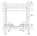
この問題点を解決するために、図4に示すように、ひとつの画素電極407に対して複数のTFT405、406を配置し、冗長性を確保することによって、対策をおこなっていた。すなわち図4のTFT406が不良素子であった場合、レーザーなどを使用してドレイン端子を408のレーザー部分で切断し、欠陥を対策していた。なお、図4において、401、402がゲイト線であり、403、404がソース線である。
【0007】
また、不良素子の判別には図5に示すような、方法で検査が行われていた。図5には、ゲイト線501、502と、ソース線503、504と、共通電極線505と、TFT506〜509と、保持容量510、511と、スイッチ512〜515と、アンプ516、517と、測定端子518、519と、電源520、521とが示されている。この場合、調べようする素子のつながるゲイト線501、502にスイッチ512、513によって、十分TFTがオンになる電圧を印加し、同時に調べようとする素子につながるソース線503、504にスイッチ514、515によって特定の電圧を印加する。つぎに、ゲイト線の電位をGNDに落とし、TFTをオフさせる。
ここでソース線に電圧印加をやめ、特定時間の間放置する、その後再度ゲイト線に電圧を印加し、ソース線の電位を測定する。TFTが正常であれば、最初のソース電位が保持容量によって保持されるため、その電圧が測定される。また、TFTのドレイン・ソースがショートであった場合、ソース線につながる抵抗を介して、放置中に放電し、測定時には電圧は変動している。またTFTがオープンの場合にはゲイト線に電圧印加されても、保持容量には電圧印加がされない。さらに、TFTの移動度やしきい値のばらつきで保持容量の充電が不十分である場合にも電圧測定を高精度で行うことによって判別が可能である。
【0008】
【発明が解決しようとする問題点】
以上にて説明した従来の液晶表示装置およびその補正方法には以下のような問題点があった。画素TFTの欠陥にたいしては補正が可能であるが、液晶材料のばらつきによる表示ムラやラビング時に発生する帯状のムラ等に関しては補正を行うことができず、液晶表示装置を不良品にしてしまうことが多かった。
【0009】
一般に、人間が表示装置を目視した場合、距離が十分離れた画素では10%以上の輝度差があっても、認識できないが、近接の画素においては、2%程度の輝度差であっても、認識される。そのため、近接画素間における輝度のばらつきをおさえることは、重要である。
また、液晶表示装置の画面サイズは近年より大きくなる方向にあり、サイズが大きくなればなるほど、画面の均一性を保つのは困難であるため、液晶表示装置の歩留まりを悪化させていた。さらに、パーソナルコンピュータやワークステーションにおいては、オペレータが長時間にわたり、至近距離で画面を見続けるため、画面むらは気になりやすく、オペレータの効率を低下させ、ユーザークレームになっていた。
【0010】
【問題を解決するための手段】
(1)本発明は、第1の記憶装置を有する表示装置と、
前記表示装置と切り離し可能な接続端子を介して接続された補正情報作成装置とを有する補正システムであって、
前記補正情報作成装置は、
前記第1の記憶装置を有する表示装置に映像を表示するための映像信号発生器と、
前記第1の記憶装置を有する表示装置に表示された映像を撮像して映像信号とする撮像装置と、
前記撮像装置から出力された前記映像信号を加工して補正情報とする信号処理装置と、
前記信号処理装置から出力された補正情報を記憶する第2の記憶装置と、
前記第2の記憶装置に記憶された補正情報と、前記信号処理装置から出力された補正情報を加算する第1の加算回路と、
前記第1の加算回路から出力された補正情報を記憶する第3の記憶装置と、
前記第3の記憶装置に記憶された補正情報と、前記信号処理装置から出力された補正情報を加算する第2の加算回路と、
前記信号処理装置から出力された補正情報、前記第1の加算回路から出力された補正情報、または前記第2の加算回路から出力された補正情報を前記第1の記憶装置に書き込む書き込み装置を含み、
前記第1の記憶装置を有する表示装置は、前記補正情報作成装置に設けられた前記映像信号発生器から出力された映像信号と前記第1の記憶装置に書き込まれた補正情報とを演算する補正演算回路を含むことを特徴とする。
(2)また本発明は、第1の記憶装置を有するアクティブマトリクス型液晶表示装置と、
前記アクティブマトリクス型液晶表示装置と切り離し可能な接続端子を介して接続された補正情報作成装置とを有する補正システムであって、
前記補正情報作成装置は、
前記第1の記憶装置を有するアクティブマトリクス型液晶表示装置に映像を表示するための映像信号発生器と、
前記第1の記憶装置を有するアクティブマトリクス型液晶表示装置に表示された映像を撮像して映像信号とする撮像装置と、
前記撮像装置から出力された前記映像信号を加工して補正情報とする信号処理装置と、
前記信号処理装置から出力された補正情報を記憶する第2の記憶装置と、
前記第2の記憶装置に記憶された補正情報と、前記信号処理装置から出力された補正情報を加算する第1の加算回路と、
前記第1の加算回路から出力された補正情報を記憶する第3の記憶装置と、
前記第3の記憶装置に記憶された補正情報と、前記信号処理装置から出力された補正情報を加算する第2の加算回路と、
前記信号処理装置から出力された補正情報、前記第1の加算回路から出力された補正情報、または前記第2の加算回路から出力された補正情報を前記第1の記憶装置に書き込む書き込み装置を含み、
前記第1の記憶装置を有するアクティブマトリクス型液晶表示装置は、前記補正情報作成装置に設けられた前記映像信号発生器から出力された映像信号と前記第1の記憶装置に書き込まれた補正情報とを演算する補正演算回路を含むことを特徴とする。
(3)また本発明は、補正情報作成装置に設けられた映像信号発生器により第1の映像信号を作成し、
切り離し可能な第1の接続端子を介して前記補正情報作成装置から第1の記憶装置を有する表示装置に前記第1の映像信号を入力し、
前記第1の映像信号をもとに前記第1の記憶装置を有する表示装置に表示された第1の映像を前記補正情報作成装置に設けられた撮像装置により撮像して第2の映像信号とし、
前記撮像装置から出力された第2の映像信号を前記補正情報作成装置に設けられた信号処理装置により加工して第1の補正情報とし、
前記信号処理装置から出力された前記第1の補正情報を切り離し可能な第2の接続端子を介して前記第1の記憶装置と、前記補正情報作成装置に設けられた第2の記憶装置とに書き込み、
前記第1の記憶装置に書き込まれた前記第1の補正情報と、前記第1の映像信号をもとに前記表示装置において映像を表示し、
前記撮像装置を用いてこの映像を撮像して第3の映像信号とし、
前記第2の記憶装置に書き込まれた前記第1の補正情報と、前記信号処理装置から出力された補正情報とを加算して第2の補正情報とし、
切り離し可能な第2の接続端子を介して前記第1の記憶装置と、前記補正情報作成装置に設けられた第3の記憶装置とに前記第2の補正情報を書き込み、
前記第1の記憶装置に書き込まれた前記第2の補正情報と、前記第1の映像信号をもとに前記表示装置において映像を表示し、
前記撮像装置を用いてこの映像を撮像して第4の映像信号とし、
前記第3の記憶装置に書き込まれた前記第2の補正情報と、前記信号処理装置から出力された補正情報とを加算して第3の補正情報とし、
前記第3の補正情報を切り離し可能な第2の接続端子を介して前記第1の記憶装置に書き込むことを特徴とする。
本発明では液晶表示装置に画素の補正内容を記憶する記憶装置を有し、その記憶装置に外部の撮像装置より得られた補正内容を記憶することによって補正を行い良好な表示をえることができる。
【0011】
【実施例】
〔参考例1〕
参考例を図1に示す。以下図面をもちいて詳細な説明をおこなう。
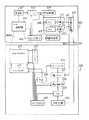
この参考例の補正システムは記憶装置(ここでは補正メモリ115)を有する液晶表示装置110とその表示装置の補正のための補正情報を作成し、記憶装置に書き込む補正情報作成装置100によって構成される。その両者は接続端子108、109を介して接続されている。
一つの液晶表示装置にたいして補正をおこない、それが終了すると、接続を切り放し、他の液晶表示装置を接続し、つぎの補正を行う。
【0012】
補正情報作成装置100内部の映像信号発生器107より出力された映像信号は液晶表示装置110の内部の同期分離回路118を介してA/Dコンバータ
117に入力され、そこでデジタル変換される。デジタル変換された映像信号は補正演算回路116に入力されるが、初期段階では補正は行わず、そのままD/Aコンバータ120に入力され、アナログ変換される。その後、ソースドライバー113を介して、アクティブマトリクス111に入力され、表示をおこなう。この段階では従来の液晶表示装置となんら変わるものではない。
【0013】
補正情報の作成は以下の様に行う。液晶表示装置110の光学表示内容は補正情報作成装置内のCCDカメラなどを備えた撮像装置101によって撮像される、撮像装置101の出力映像信号は一般的には微弱な信号であるため増幅器102で増幅されたのち、A/Dコンバータ103によってデジタル変換され、信号処理装置104に入力される。
【0014】
信号処理装置104では映像信号中に含まれるノイズ成分やモアレ成分を除去して液晶表示装置110の画素の欠陥やむらの情報のみを検出する。欠陥やむらの検出が行いやすいようにアクティブマトリクス111に表示する表示内容は単一色かつ同一輝度であることが望ましい。
欠陥やむらを検出するための方法としては、信号処理装置104において、ある一定基準レベルと信号処理装置の入力信号の差をとり、その値を補正値とする方法やメディアンフィルタを使用し入力信号のゆるやかな変化を抽出し、もとの信号から抽出結果を減算して、特異点を検出する方法や、ラプラシアンフィルタを使用し入力信号の急峻な変化を抽出し、特異点を検出する方法をもちいても良い。 ただし、メディアンフィルタやラプラシアンフィルタを使用して特異点を検出する場合には、言うまでもなく補正情報は特異点のみの情報となるため、表示装置の輝度の緩やかな変化については対応しない。しかし、これは前述した様に人間の目の感覚が緩やかな変化に関しては鈍感であることより、実用上の不具合にはならない。
【0015】
信号処理装置104の出力は書き込み装置105によって、液晶表示装置110内の補正メモリ115に書き込まれる。書き込み方法はメモリコントローラ114で制御される補正メモリ115の種類に応じて必要な方法で実行される。
【0016】
補正メモリ115への書き込みが終了した段階で補正作業は終了する。
補正作業終了後、液晶表示装置110に映像信号が入力され、表示を行う場合においては、映像信号は同期分離装置118を経てA/Dコンバータ117でデジタル変換されたのち、補正演算回路116で補正メモリ115の出力信号と演算され、補正を受けた後、D/Aコンバータ120を介してソースドラーバー113に入力される。ゲイトドライバーは、クロックジェネレータ119で制御される。ここで、アクティブマトリクスは補正された映像を光学表示する。なお各構成要素は、クロックジェネレータ106と119とによって制御される。
【0017】
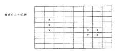
本発明による表示情報を記載した例を図7〜図15に示す
図7は補正を行う前の表示装置111の表示結果である。ここでは8×8のマトリクスを例にしているが、値は任意で問題ない。Xの印がムラの箇所である。この例では輝度を0から100まで区分し、表示すべき輝度は一律に50であるものとしている。
【0018】
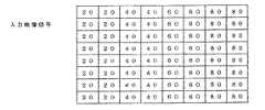
図8は図7の表示結果を撮像し、デジタル化した表示の情報の例である。ムラの発生している場所は周囲とくらべて数値が離れている。また、表示画面全体としては、左上から右下にむけて緩やかに数値が変化しているが、前述したように人間の視覚上は変化が緩やかであれば問題ない。
【0019】
図9は表示すべき輝度すなわち50と図8の差分をとったものである。この差分検出は信号処理装置106でおこなわれる。この場合は図9が補正情報となる。
【0020】
図10は補正情報作成後に、新たに表示を行うべき映像信号をデジタル化したものでA/Dコンバータ117の出力情報である。
【0021】
図11は図10と図9の情報を補正演算回路116で加算したもので補正演算装置116の出力情報である。この値を表示装置111に入力すると表示装置111の表示ムラが相殺され、本来表示すべき映像信号の情報図10が表示される。
【0022】
また、信号処理装置104において、単なる減算処理ではなく、図8をメディアンフィルタを通過させたものが図12であり、図12と図8を減算処理したものが図13である。この場合は図13が補正情報となる。メディアンフィルタはここでは緩やかな変化のみを通過させ、ムラの情報を除去している。このムラ除去後の情報ともとの情報を減算する事により、ムラの情報がひきだせる。
【0023】
また、ラプラシアンフィルタをもちいれば、急激な変化点の情報をひきだせる。図13の情報を補正演算回路116で図10と加算したものが、図14であり補正演算装置116の出力情報である。図14を表示装置111に入力した結果、得られる表示情報は図15となり、緩やかな変化はあるものの、急峻な変化はなくなり、ムラをめだたなくする事が可能である。
【0024】
この参考例ではアナログ諧調のドライバーを想定しているが、これはデジタル諧調のドライバーを使用してもよい、ただし、この場合には、D/Aコンバータ120は不要である。また映像信号発生器107がデジタル出力であり、且つ液晶表示装置110への映像信号入力がデジタルの場合はA/Dコンバータ117も不要である。
【0025】
ここに使用する補正メモリはEPROM、EEPROM、フラッシュメモリなど不揮発性メモリであればよい、これらのメモリは液晶表示用装置110のガラス上にCOG技術によって装着しても良いし、ガラスとは別に基板実装しても良い。また、画素TFTを駆動する駆動回路はTFTをもちいてガラス基板上にアクティブマトリクスと同時形成して製作しても良いし、メモリと同様に単結晶チップをCOGで実装しても良いし、TABを用いても良い。
【0026】
〔実施例1〕
図6は発明の実施例である。この実施例では参考例とは異なり撮像と補正を複数回行っている。以下図6の説明を行う。この実施例に示す補正システムは、記憶装置(ここでは補正メモリ625)を有する液晶表示装置620とその表示装置の補正のための補正情報を作成し、記憶装置に書き込む補正情報作成装置600によって構成される。その両者は接続端子613、614を介して接続されている。
一つの液晶表示装置に対して補正をおこない、それが終了すると、接続を切り放し、他の液晶表示装置を接続し、つぎの補正を行う。
【0027】
補正情報作成装置600内部の映像信号発生器607より出力された映像信号は液晶表示装置620の内部の同期分離回路628を介してA/Dコンバータ
627に入力され、そこでデジタル変換される。デジタル変換された映像信号は補正演算回路626に入力されるが、初期段階では補正は行わず、そのままD/Aコンバータ630に入力され、アナログ変換される。その後、ソースドライバー623を介して、アクティブマトリクス621に入力され、表示をおこなう。この段階では従来の液晶表示装置となんら変わるものではない。
【0028】
補正情報の作成は以下の様に行う。液晶表示装置620の光学表示内容は補正情報作成装置内のCCDカメラなどを備えた撮像装置601によって撮像される、撮像装置601の出力映像信号は一般的には微弱な信号であるため増幅器602で増幅されたのち、A/Dコンバータ603によってデジタル変換され、信号処理装置604に入力される。
【0029】
以下の動作方法を示す。第一回目の撮像において、信号処理装置604で得られた補正情報はスイッチ612と信号書き込み装置605を介して補正メモリ625に記憶されるだけでなく、メモリ608に記憶される。参考例と同様にして画面の補正をおこなった後、再度、表示を行い、第二回目の撮像を行う、ここで信号処理装置604でえられた情報はメモリ608に記憶された第一回目の補正情報と加算してメモリ609に記憶されるとともに再度補正メモリ625に記憶され、液晶表示装置は再補正される。さらに、表示を行い、第三回目の撮像を行う。信号処理装置604の出力情報はメモリ609に記憶された第二回目の補正情報と加算され、信号書き込み装置605を介して補正メモリ625に記憶される。
【0030】
このようにして、撮像と補正を複数回繰り返すことにより、より高精度な補正が可能となる。この例では3回の補正を行っているが、4回以上補正をおこなってもかまわない。また、補正メモリやアクティブマトリクスの駆動については、参考例と同じである。
【0031】
本発明は従来の画素TFTに冗長性をもたせることによって補正を行う従来の補正方法と背反するものでは無く、従来の補正方法と組み合わせることによって、よりいっそう効果を得ることができるものである。
【0032】
【発明の効果】
以上述べたように、本発明では液晶表示装置に内蔵した記憶装置にその液晶表示装置の欠陥やムラの情報を記憶し、その情報と液晶表示装置に入力される映像信号とを演算し、欠陥やムラを補正することによってより、高品質な表示を行うことが可能であるという効果がある。
【図面の簡単な説明】
【図1】 本発明の第一の実施例
【図2】 アクティブマトリクスLCDの従来例
【図3】 TFTの動作波形
【図4】 従来の画素領域の平面図
【図5】 従来のアクティブマトリクスの検査回路
【図6】 本発明の第二の実施例
【図7】 表示情報を記載した例
【図8】 表示情報を記載した例
【図9】 表示情報を記載した例
【図10】 表示情報を記載した例
【図11】 表示情報を記載した例
【図12】 表示情報を記載した例
【図13】 表示情報を記載した例
【図14】 表示情報を記載した例
【図15】 表示情報を記載した例
【符号の説明】
ソースドライバー 201
ゲイトドライバー 202
ソース線 203〜205
ゲイト線 206〜208
TFT 209〜212
保持容量 213〜216
液晶 217〜220
アクティブマトリクス 221
a)ソース端子電位波形
b)ゲイト端子電位波形
c)ドレイン端子電位波形
ゲイト線 401、402
ソース線 403、404
TFT 405、406
画素電極 407
レーザー切断部 408
ゲイト線 501、502
ソース線 503、504
共通電極線 505
TFT 506〜509
保持容量 510、511
スイッチ 512〜515
アンプ 516、517
測定端子 518、519
電源 520、521
メモリ 115
液晶表示装置 110
情報作成装置 100
接続端子 108、109
映像信号発生器 107
同期分離回路 118
A/Dコンバータ 117
補正演算回路 116
D/Aコンバータ 120
アクティブマトリクス 111
撮像装置 101
増幅器 102
A/Dコンバータ 103
信号処理装置 104
補正メモリ 115
メモリコントローラ 114
クロックジェネレーター 106、119[0001]
[Industrial application fields]
The present invention relates to a display correction system for a display device, particularly a display device having a nonvolatile storage device, and a correction method thereof.
[0002]
[Prior art]
Conventional display devices include CRTs, plasma displays, liquid crystal display devices, and the like. In recent years, development of liquid crystal display devices, particularly active matrix liquid crystal display devices, has been actively conducted.
[0003]
The liquid crystal display device uses the fact that the liquid crystal substance has different dielectric constants in the direction parallel to and perpendicular to the molecular axis, and displays ON / OFF, that is, light and dark by controlling the amount of light transmitted or scattered. As the liquid crystal material, TN liquid crystal, STN liquid crystal, ferroelectric liquid crystal and the like are common.
[0004]
Among display devices using liquid crystal, an active matrix liquid crystal display device is said to have excellent display characteristics. As shown in FIG. 2, in a conventional active matrix type liquid crystal display device,
Since a voltage is applied from the pixel electrode to the liquid crystal by such a method, it is possible to realize a liquid crystal display device having a small contrast and a high contrast with respect to adjacent pixels.
[0005]
Since the active matrix liquid crystal display device described above requires as many TFTs as the number of pixels, when a TFT element in the substrate surface is defective and the TFT becomes open or short-circuited, the pixel at that point is a specific pixel. Since the potential is fixed or the potential becomes unstable, the pixel appears as a point defect on the panel. In addition, the voltage value applied to the pixel electrode varies due to variations in the threshold value and mobility of the TFT, resulting in variations in pixel luminance.
[0006]
In order to solve this problem, as shown in FIG. 4, a plurality of
[0007]
Further, in order to determine a defective element, an inspection is performed by a method as shown in FIG. FIG. 5 shows
Here, the voltage application to the source line is stopped and left for a specific time, and then the voltage is applied to the gate line again to measure the potential of the source line. If the TFT is normal, the initial source potential is held by the holding capacitor, and the voltage is measured. Further, when the drain / source of the TFT is short-circuited, it is discharged while being left through a resistor connected to the source line, and the voltage fluctuates during measurement. When the TFT is open, no voltage is applied to the storage capacitor even if a voltage is applied to the gate line. Further, even when the storage capacitor is insufficiently charged due to variations in TFT mobility or threshold, it is possible to make a determination by performing voltage measurement with high accuracy.
[0008]
[Problems to be solved by the invention]
The conventional liquid crystal display device described above and its correction method have the following problems. Although it is possible to correct the defect of the pixel TFT, it is not possible to correct the display unevenness due to the variation of the liquid crystal material or the strip-like unevenness generated at the time of rubbing, and the liquid crystal display device may be defective. There were many.
[0009]
In general, when a human visually observes a display device, even if there is a luminance difference of 10% or more in a pixel that is sufficiently far away, it cannot be recognized, but in a neighboring pixel, even if the luminance difference is about 2%, Be recognized. For this reason, it is important to suppress variation in luminance between adjacent pixels.
In addition, the screen size of the liquid crystal display device has been increasing in recent years, and the larger the size, the more difficult it is to maintain the uniformity of the screen, so the yield of the liquid crystal display device has been deteriorated. Furthermore, in personal computers and workstations, since the operator continues to look at the screen at a close distance for a long time, the screen unevenness tends to be anxious, reducing the efficiency of the operator and causing user complaints.
[0010]
[Means for solving problems]
(1) The present invention provides a display device having a first storage device;
A correction system having a correction information creation device connected via a connection terminal that can be separated from the display device,
The correction information creation device includes:
A video signal generator for displaying video on a display device having the first storage device;
An imaging device that captures an image displayed on a display device having the first storage device to obtain a video signal;
A signal processing device that processes the video signal output from the imaging device to obtain correction information;
A second storage device for storing correction information output from the signal processing device;
A first addition circuit for adding the correction information stored in the second storage device and the correction information output from the signal processing device;
A third storage device for storing correction information output from the first addition circuit;
A second addition circuit for adding the correction information stored in the third storage device and the correction information output from the signal processing device;
A writing device that writes the correction information output from the signal processing device, the correction information output from the first addition circuit, or the correction information output from the second addition circuit to the first storage device; ,
The display device having the first storage device corrects the video signal output from the video signal generator provided in the correction information generation device and the correction information written in the first storage device. An arithmetic circuit is included.
(2) The present invention also provides an active matrix liquid crystal display device having a first storage device;
A correction system having a correction information generating device connected to the active matrix liquid crystal display device through a detachable connection terminal,
The correction information creation device includes:
A video signal generator for displaying video on an active matrix liquid crystal display device having the first storage device;
An imaging device that captures an image displayed on an active matrix liquid crystal display device having the first storage device to generate an image signal;
A signal processing device that processes the video signal output from the imaging device to obtain correction information;
A second storage device for storing correction information output from the signal processing device;
A first addition circuit for adding the correction information stored in the second storage device and the correction information output from the signal processing device;
A third storage device for storing correction information output from the first addition circuit;
A second addition circuit for adding the correction information stored in the third storage device and the correction information output from the signal processing device;
A writing device that writes the correction information output from the signal processing device, the correction information output from the first addition circuit, or the correction information output from the second addition circuit to the first storage device; ,
An active matrix liquid crystal display device having the first storage device includes a video signal output from the video signal generator provided in the correction information generation device, and correction information written in the first storage device. It includes a correction arithmetic circuit for calculating.
(3) In the present invention, the first video signal is created by the video signal generator provided in the correction information creation device,
The first video signal is input from the correction information creation device to the display device having the first storage device via the detachable first connection terminal,
Based on the first video signal, the first video displayed on the display device having the first storage device is picked up by the imaging device provided in the correction information creating device to be a second video signal. ,
The second video signal output from the imaging device is processed by the signal processing device provided in the correction information creation device to be the first correction information,
The first storage device and the second storage device provided in the correction information generation device via a second connection terminal capable of separating the first correction information output from the signal processing device. writing,
Displaying video on the display device based on the first correction information written in the first storage device and the first video signal;
This image is imaged using the imaging device as a third image signal,
The first correction information written in the second storage device and the correction information output from the signal processing device are added to obtain second correction information,
Write the second correction information to the first storage device and the third storage device provided in the correction information creation device via a detachable second connection terminal,
Displaying a video on the display device based on the second correction information written in the first storage device and the first video signal;
This image is imaged using the imaging device to form a fourth image signal,
The second correction information written in the third storage device and the correction information output from the signal processing device are added to obtain third correction information,
The third correction information is written to the first storage device via a second connection terminal that can be separated.
In the present invention, the liquid crystal display device has a storage device that stores pixel correction contents, and the storage device stores correction contents obtained from an external imaging device to perform correction and obtain a good display. .
[0011]
【Example】
[Reference Example 1]
A reference example is shown in FIG. A detailed description will be given below with reference to the drawings.
The correction system of thisreference example includes a liquid
Correction is performed on one liquid crystal display device. When the correction is completed, the connection is disconnected, another liquid crystal display device is connected, and the next correction is performed.
[0012]
The video signal output from the
[0013]
The correction information is created as follows. The optical display content of the liquid
[0014]
The
As a method for detecting defects and unevenness, in the
[0015]
The output of the
[0016]
The correction work ends when the writing to the correction memory 115 is completed.
When the video signal is input to the liquid
[0017]
Examples showing display information according to the present invention shown in FIGS. 7 to 15 are display results of the display device 111 before correction. Here, an 8 × 8 matrix is taken as an example, but the value is arbitrary and does not cause any problem. The mark of X is a spot of unevenness. In this example, the luminance is divided from 0 to 100, and the luminance to be displayed is uniformly 50.
[0018]
FIG. 8 is an example of display information obtained by imaging and digitizing the display result of FIG. The place where unevenness occurs is far from the surroundings. The numerical value of the display screen as a whole gradually changes from the upper left to the lower right. However, as described above, there is no problem if the change is gentle on human vision.
[0019]
FIG. 9 shows the luminance to be displayed, that is, the difference between 50 and FIG. This difference detection is performed by the
[0020]
FIG. 10 shows the output information of the A / D converter 117, which is a digitized video signal to be displayed after the correction information is created.
[0021]
FIG. 11 shows the output information of the correction arithmetic unit 116 obtained by adding the information of FIGS. 10 and 9 by the correction arithmetic circuit 116. When this value is input to the display device 111, the display unevenness of the display device 111 is canceled, and the information diagram 10 of the video signal to be originally displayed is displayed.
[0022]
Further, in the
[0023]
In addition, if a Laplacian filter is used, information on sudden change points can be extracted. The information of FIG. 13 added to that of FIG. 10 by the correction arithmetic circuit 116 is FIG. 14 and is output information of the correction arithmetic device 116. As a result of inputting FIG. 14 to the display device 111, the obtained display information is as shown in FIG. 15, and although there is a gradual change, there is no steep change and it is possible to make the unevenness unnoticeable.
[0024]
In thisreference example, an analog gradation driver is assumed, but a digital gradation driver may be used. However, in this case, the D / A converter 120 is unnecessary. Further, when the
[0025]
The correction memory used here may be a non-volatile memory such as an EPROM, an EEPROM, a flash memory, etc. These memories may be mounted on the glass of the liquid
[0026]
[Example1 ]
FIG. 6 showsan embodiment of the invention. In this embodiment, unlike thereference example, imaging and correction are performed a plurality of times. The description of FIG. 6 will be given below.The correction system shown inthis embodiment includes a liquid
Correction is performed on one liquid crystal display device. When the correction is completed, the connection is disconnected, another liquid crystal display device is connected, and the next correction is performed.
[0027]
The video signal output from the video signal generator 607 in the correction
[0028]
The correction information is created as follows. The optical display content of the liquid
[0029]
The following operation method is shown. In the first imaging, correction information obtained by the
[0030]
In this way, it is possible to perform more accurate correction by repeating imaging and correction a plurality of times. Is performed three times of correction in thisexample, it may be subjected to correction more than4 times. Further, the correction memory and the active matrix are driven in the samemanner as in thereference example.
[0031]
The present invention is not contrary to the conventional correction method in which correction is performed by providing redundancy to the conventional pixel TFT, and further effects can be obtained by combining with the conventional correction method.
[0032]
【The invention's effect】
As described above, according to the present invention, information on defects and unevenness of the liquid crystal display device is stored in the storage device built in the liquid crystal display device, and the information and the video signal input to the liquid crystal display device are calculated. In addition, there is an effect that higher quality display can be performed by correcting the unevenness.
[Brief description of the drawings]
FIG. 1 First Embodiment of the Invention FIG. 2 Conventional Example of Active Matrix LCD FIG. 3 TFT Operation Waveform FIG. 4 Plan View of Conventional Pixel Region FIG. 5 Conventional Active Matrix Inspection circuit [FIG. 6] Second embodiment of the present invention [FIG. 7] Example in which display information is described [FIG. 8] Example in which display information is described [FIG. 9] Example in which display information is described [FIG. 10] Display information [Fig. 11] Example of display information [Fig. 12] Example of display information [Fig. 13] Example of display information [Fig. 14] Example of display information [Fig. 15] Display information Example of description [Explanation of symbols]
Source line 203-205
Gate line 206-208
TFT 209-212
Retention capacity 213-216
Liquid crystal 217-220
Active matrix 221
a) Source terminal potential waveform b) Gate terminal potential waveform c) Drain terminal potential
TFT 506-509
Holding capacity 510,511
Switch 512-515
Amplifier 516,517
Memory 115
Liquid
Sync separation circuit 118
A / D converter 117
Correction arithmetic circuit 116
D / A converter 120
Active matrix 111
Imaging device 101
A /
Correction memory 115
Claims (3)
Translated fromJapanese前記表示装置と切り離し可能な接続端子を介して接続された補正情報作成装置とを有する補正システムであって、
前記補正情報作成装置は、
前記第1の記憶装置を有する表示装置に映像を表示するための映像信号発生器と、
前記第1の記憶装置を有する表示装置に表示された映像を撮像して映像信号とする撮像装置と、
前記撮像装置から出力された前記映像信号を加工して補正情報とする信号処理装置と、
前記信号処理装置から出力された補正情報を記憶する第2の記憶装置と、
前記第2の記憶装置に記憶された補正情報と、前記信号処理装置から出力された補正情報を加算する第1の加算回路と、
前記第1の加算回路から出力された補正情報を記憶する第3の記憶装置と、
前記第3の記憶装置に記憶された補正情報と、前記信号処理装置から出力された補正情報を加算する第2の加算回路と、
前記信号処理装置から出力された補正情報、前記第1の加算回路から出力された補正情報、または前記第2の加算回路から出力された補正情報を前記第1の記憶装置に書き込む書き込み装置を含み、
前記第1の記憶装置を有する表示装置は、前記補正情報作成装置に設けられた前記映像信号発生器から出力された映像信号と前記第1の記憶装置に書き込まれた補正情報とを演算する補正演算回路を含むことを特徴とする補正システム。A display device having a first storage device;
A correction system having a correction information creation device connected via a connection terminal that can be separated from the display device,
The correction information creation device includes:
A video signal generator for displaying video on a display device having the first storage device;
An imaging device that captures an image displayed on a display device having the first storage device to obtain a video signal;
A signal processing device that processes the video signal output from the imaging device to obtain correction information;
A second storage device for storing correction information output from the signal processing device;
A first addition circuit for adding the correction information stored in the second storage device and the correction information output from the signal processing device;
A third storage device for storing correction information output from the first addition circuit;
A second addition circuit for adding the correction information stored in the third storage device and the correction information output from the signal processing device;
A writing device that writes the correction information output from the signal processing device, the correction information output from the first addition circuit, or the correction information output from the second addition circuit to the first storage device; ,
The display device having the first storage device corrects the video signal output from the video signal generator provided in the correction information generation device and the correction information written in the first storage device. A correction system including an arithmetic circuit.
前記アクティブマトリクス型液晶表示装置と切り離し可能な接続端子を介して接続された補正情報作成装置とを有する補正システムであって、
前記補正情報作成装置は、
前記第1の記憶装置を有するアクティブマトリクス型液晶表示装置に映像を表示するための映像信号発生器と、
前記第1の記憶装置を有するアクティブマトリクス型液晶表示装置に表示された映像を撮像して映像信号とする撮像装置と、
前記撮像装置から出力された前記映像信号を加工して補正情報とする信号処理装置と、
前記信号処理装置から出力された補正情報を記憶する第2の記憶装置と、
前記第2の記憶装置に記憶された補正情報と、前記信号処理装置から出力された補正情報を加算する第1の加算回路と、
前記第1の加算回路から出力された補正情報を記憶する第3の記憶装置と、
前記第3の記憶装置に記憶された補正情報と、前記信号処理装置から出力された補正情報を加算する第2の加算回路と、
前記信号処理装置から出力された補正情報、前記第1の加算回路から出力された補正情報、または前記第2の加算回路から出力された補正情報を前記第1の記憶装置に書き込む書き込み装置を含み、
前記第1の記憶装置を有するアクティブマトリクス型液晶表示装置は、前記補正情報作成装置に設けられた前記映像信号発生器から出力された映像信号と前記第1の記憶装置に書き込まれた補正情報とを演算する補正演算回路を含むことを特徴とする補正システム。An active matrix liquid crystal display device having a first storage device;
A correction system having a correction information generating device connected to the active matrix liquid crystal display device through a detachable connection terminal,
The correction information creation device includes:
A video signal generator for displaying video on an active matrix liquid crystal display device having the first storage device;
An imaging device that captures an image displayed on an active matrix liquid crystal display device having the first storage device to generate an image signal;
A signal processing device that processes the video signal output from the imaging device to obtain correction information;
A second storage device for storing correction information output from the signal processing device;
A first addition circuit for adding the correction information stored in the second storage device and the correction information output from the signal processing device;
A third storage device for storing correction information output from the first addition circuit;
A second addition circuit for adding the correction information stored in the third storage device and the correction information output from the signal processing device;
A writing device that writes the correction information output from the signal processing device, the correction information output from the first addition circuit, or the correction information output from the second addition circuit to the first storage device; ,
An active matrix liquid crystal display device having the first storage device includes a video signal output from the video signal generator provided in the correction information generation device, and correction information written in the first storage device. A correction system comprising a correction arithmetic circuit for calculating
切り離し可能な第1の接続端子を介して前記補正情報作成装置から第1の記憶装置を有する表示装置に前記第1の映像信号を入力し、
前記第1の映像信号をもとに前記第1の記憶装置を有する表示装置に表示された第1の映像を前記補正情報作成装置に設けられた撮像装置により撮像して第2の映像信号とし、
前記撮像装置から出力された第2の映像信号を前記補正情報作成装置に設けられた信号処理装置により加工して第1の補正情報とし、
前記信号処理装置から出力された前記第1の補正情報を切り離し可能な第2の接続端子を介して前記第1の記憶装置と、前記補正情報作成装置に設けられた第2の記憶装置とに書き込み、
前記第1の記憶装置に書き込まれた前記第1の補正情報と、前記第1の映像信号をもとに前記表示装置において映像を表示し、
前記撮像装置を用いてこの映像を撮像して第3の映像信号とし、
前記第2の記憶装置に書き込まれた前記第1の補正情報と、前記信号処理装置から出力された補正情報とを加算して第2の補正情報とし、
切り離し可能な第2の接続端子を介して前記第1の記憶装置と、前記補正情報作成装置に設けられた第3の記憶装置とに前記第2の補正情報を書き込み、
前記第1の記憶装置に書き込まれた前記第2の補正情報と、前記第1の映像信号をもとに前記表示装置において映像を表示し、
前記撮像装置を用いてこの映像を撮像して第4の映像信号とし、
前記第3の記憶装置に書き込まれた前記第2の補正情報と、前記信号処理装置から出力された補正情報とを加算して第3の補正情報とし、
前記第3の補正情報を切り離し可能な第2の接続端子を介して前記第1の記憶装置に書き込むことを特徴とした補正システムの動作方法。A first video signal is created by a video signal generator provided in the correction information creation device,
The first video signal is input from the correction information creation device to the display device having the first storage device via the detachable first connection terminal,
Based on the first video signal, the first video displayed on the display device having the first storage device is picked up by the imaging device provided in the correction information creating device to be a second video signal. ,
The second video signal output from the imaging device is processed by the signal processing device provided in the correction information creation device to be the first correction information,
The first storage device and the second storage device provided in the correction information generation device via a second connection terminal capable of separating the first correction information output from the signal processing device. writing,
Displayingvideo on the display device based on the first correction information written in the first storage device and the first video signal;
This image is imaged using the imaging device as a third image signal,
Apre-SL and the first correction information written in the second storage device,the second correction information by adding thecorrection information output from the signal processing unit,
Writethe second correction information to thefirst storage device and the third storage device provided in the correction information creation device via a detachable second connection terminal,
Displaying avideo on the display device based onthe second correction information written in the first storage device and the first video signal;
This image is imaged using the imaging device to form a fourth image signal,
Saidsecond correction informationpreviously written Symbol third storage device, adds thecorrection information output from said signal processing device and athird correction information,
An operation method of a correction system, whereinthe third correction information is written to the first storage device through a second connection terminal that can be separated.
Priority Applications (12)
| Application Number | Priority Date | Filing Date | Title |
|---|---|---|---|
| JP07953394AJP3672586B2 (en) | 1994-03-24 | 1994-03-24 | Correction system and operation method thereof |
| US08/407,685US5793344A (en) | 1994-03-24 | 1995-03-21 | System for correcting display device and method for correcting the same |
| TW084102783ATW269033B (en) | 1994-03-24 | 1995-03-22 | |
| KR1019950006290AKR100272821B1 (en) | 1994-03-24 | 1995-03-24 | Display system correction system and its correction method |
| CN95104532ACN1089522C (en) | 1994-03-24 | 1995-03-24 | Apparatus and method for calibrating a display device |
| CNB2004100322069ACN100381921C (en) | 1994-03-24 | 1995-03-24 | Method for correcting video signal by active matrix display device |
| CNB2006101014098ACN100520900C (en) | 1994-03-24 | 1995-03-24 | Method for operating active-matrix display |
| US09/104,978US6549183B1 (en) | 1994-03-24 | 1998-06-26 | System for correcting display device method for correcting the same and method of manufacturing the system |
| KR1020000031595AKR100305276B1 (en) | 1994-03-24 | 2000-06-09 | A correction system and a method for operating the system |
| CNB011394374ACN1149528C (en) | 1994-03-24 | 2001-11-20 | Method for operating a correction system |
| US10/406,318US6987497B2 (en) | 1994-03-24 | 2003-04-04 | System for correcting display device and method for correcting the same |
| US11/322,342US20060109231A1 (en) | 1994-03-24 | 2006-01-03 | System for correcting display device and method for correcting the same |
Applications Claiming Priority (1)
| Application Number | Priority Date | Filing Date | Title |
|---|---|---|---|
| JP07953394AJP3672586B2 (en) | 1994-03-24 | 1994-03-24 | Correction system and operation method thereof |
Related Child Applications (2)
| Application Number | Title | Priority Date | Filing Date |
|---|---|---|---|
| JP2000209018ADivisionJP2001075542A (en) | 2000-07-10 | 2000-07-10 | Correction system and its operating method |
| JP2000209020ADivisionJP2001075523A (en) | 2000-07-10 | 2000-07-10 | Correction system and its operating method |
Publications (2)
| Publication Number | Publication Date |
|---|---|
| JPH07261719A JPH07261719A (en) | 1995-10-13 |
| JP3672586B2true JP3672586B2 (en) | 2005-07-20 |
Family
ID=13692637
Family Applications (1)
| Application Number | Title | Priority Date | Filing Date |
|---|---|---|---|
| JP07953394AExpired - Fee RelatedJP3672586B2 (en) | 1994-03-24 | 1994-03-24 | Correction system and operation method thereof |
Country Status (5)
| Country | Link |
|---|---|
| US (4) | US5793344A (en) |
| JP (1) | JP3672586B2 (en) |
| KR (2) | KR100272821B1 (en) |
| CN (4) | CN100520900C (en) |
| TW (1) | TW269033B (en) |
Families Citing this family (104)
| Publication number | Priority date | Publication date | Assignee | Title |
|---|---|---|---|---|
| JP3672586B2 (en)* | 1994-03-24 | 2005-07-20 | 株式会社半導体エネルギー研究所 | Correction system and operation method thereof |
| TW290678B (en) | 1994-12-22 | 1996-11-11 | Handotai Energy Kenkyusho Kk | |
| US6069600A (en)* | 1996-03-28 | 2000-05-30 | Kabushiki Kaisha Toshiba | Active matrix type liquid crystal display |
| US6697037B1 (en)* | 1996-04-29 | 2004-02-24 | International Business Machines Corporation | TFT LCD active data line repair |
| JPH09318929A (en)* | 1996-05-29 | 1997-12-12 | Toshiba Corp | Liquid crystal display device and display unevenness correction method |
| JP2937130B2 (en)* | 1996-08-30 | 1999-08-23 | 日本電気株式会社 | Active matrix type liquid crystal display |
| US6166782A (en)* | 1997-01-29 | 2000-12-26 | Apple Computer, Inc. | Method and apparatus for reducing visibility of damping wires in aperture grill display tubes |
| US6667494B1 (en)* | 1997-08-19 | 2003-12-23 | Semiconductor Energy Laboratory Co., Ltd. | Semiconductor device and semiconductor display device |
| US6717179B1 (en)* | 1997-08-19 | 2004-04-06 | Semiconductor Energy Laboratory Co., Ltd. | Semiconductor device and semiconductor display device |
| JP3980178B2 (en)* | 1997-08-29 | 2007-09-26 | 株式会社半導体エネルギー研究所 | Nonvolatile memory and semiconductor device |
| JPH11143379A (en)* | 1997-09-03 | 1999-05-28 | Semiconductor Energy Lab Co Ltd | Semiconductor display device correction system and semiconductor display device correction method |
| US6476779B1 (en)* | 1998-03-31 | 2002-11-05 | Sony Corporation | Video display device |
| JP3632505B2 (en)* | 1999-06-18 | 2005-03-23 | セイコーエプソン株式会社 | Image display device |
| US6909411B1 (en)* | 1999-07-23 | 2005-06-21 | Semiconductor Energy Laboratory Co., Ltd. | Display device and method for operating the same |
| JP4754682B2 (en)* | 1999-11-19 | 2011-08-24 | 株式会社半導体エネルギー研究所 | Display device |
| US6618115B1 (en)* | 1999-11-19 | 2003-09-09 | Semiconductor Energy Laboratory Co., Ltd. | Defective pixel compensation system and display device using the system |
| JP2001209358A (en)* | 2000-01-26 | 2001-08-03 | Seiko Epson Corp | Unevenness correction of display image |
| US20020113268A1 (en)* | 2000-02-01 | 2002-08-22 | Jun Koyama | Nonvolatile memory, semiconductor device and method of manufacturing the same |
| US6414661B1 (en) | 2000-02-22 | 2002-07-02 | Sarnoff Corporation | Method and apparatus for calibrating display devices and automatically compensating for loss in their efficiency over time |
| US6577531B2 (en) | 2000-04-27 | 2003-06-10 | Semiconductor Energy Laboratory Co., Ltd. | Nonvolatile memory and semiconductor device |
| US7088322B2 (en) | 2000-05-12 | 2006-08-08 | Semiconductor Energy Laboratory Co., Ltd. | Semiconductor device |
| US6992652B2 (en)* | 2000-08-08 | 2006-01-31 | Semiconductor Energy Laboratory Co., Ltd. | Liquid crystal display device and driving method thereof |
| TW522374B (en)* | 2000-08-08 | 2003-03-01 | Semiconductor Energy Lab | Electro-optical device and driving method of the same |
| TW518552B (en)* | 2000-08-18 | 2003-01-21 | Semiconductor Energy Lab | Liquid crystal display device, method of driving the same, and method of driving a portable information device having the liquid crystal display device |
| US7180496B2 (en)* | 2000-08-18 | 2007-02-20 | Semiconductor Energy Laboratory Co., Ltd. | Liquid crystal display device and method of driving the same |
| US6987496B2 (en)* | 2000-08-18 | 2006-01-17 | Semiconductor Energy Laboratory Co., Ltd. | Electronic device and method of driving the same |
| TW514854B (en)* | 2000-08-23 | 2002-12-21 | Semiconductor Energy Lab | Portable information apparatus and method of driving the same |
| US7184014B2 (en)* | 2000-10-05 | 2007-02-27 | Semiconductor Energy Laboratory Co., Ltd. | Liquid crystal display device |
| US6950109B2 (en)* | 2000-10-23 | 2005-09-27 | Sun Microsystems, Inc. | Multi-spectral color correction |
| JP3899817B2 (en)* | 2000-12-28 | 2007-03-28 | セイコーエプソン株式会社 | Liquid crystal display device and electronic device |
| US6747623B2 (en) | 2001-02-09 | 2004-06-08 | Semiconductor Energy Laboratory Co., Ltd. | Liquid crystal display device and method of driving the same |
| JP3614792B2 (en)* | 2001-04-23 | 2005-01-26 | ウインテスト株式会社 | Pixel inspection apparatus and pixel inspection method for active matrix display |
| JP3606270B2 (en)* | 2001-07-09 | 2005-01-05 | セイコーエプソン株式会社 | Electro-optical device driving method, image processing circuit, electronic apparatus, and correction data generation method |
| TWI221268B (en)* | 2001-09-07 | 2004-09-21 | Semiconductor Energy Lab | Light emitting device and method of driving the same |
| TWI273539B (en) | 2001-11-29 | 2007-02-11 | Semiconductor Energy Lab | Display device and display system using the same |
| JP3913534B2 (en)* | 2001-11-30 | 2007-05-09 | 株式会社半導体エネルギー研究所 | Display device and display system using the same |
| KR100462600B1 (en)* | 2002-04-02 | 2004-12-20 | 삼성전자주식회사 | Apparatus and method for controlling automatically adjustment of power supply in a plasma display panel drive system |
| US6911781B2 (en) | 2002-04-23 | 2005-06-28 | Semiconductor Energy Laboratory Co., Ltd. | Light emitting device and production system of the same |
| KR100859514B1 (en)* | 2002-05-30 | 2008-09-22 | 삼성전자주식회사 | Liquid crystal display and its driving device |
| JP4067878B2 (en)* | 2002-06-06 | 2008-03-26 | 株式会社半導体エネルギー研究所 | Light emitting device and electric appliance using the same |
| US6982727B2 (en)* | 2002-07-23 | 2006-01-03 | Broadcom Corporation | System and method for providing graphics using graphical engine |
| TW559756B (en)* | 2002-08-26 | 2003-11-01 | Chi Mei Optoelectronics Corp | Defective pixel remedy device and method of LCD panel |
| US6933967B2 (en)* | 2002-09-10 | 2005-08-23 | Sony Corporation | Color reference system for display monitor |
| US7298355B2 (en)* | 2002-12-27 | 2007-11-20 | Semiconductor Energy Laboratory Co., Ltd. | Display device |
| US20040246280A1 (en)* | 2003-06-06 | 2004-12-09 | Credelle Thomas Lloyd | Image degradation correction in novel liquid crystal displays |
| GB2410143A (en)* | 2004-01-13 | 2005-07-20 | Hassan Paddy Abdel Salam | Display calibration cradle for portable device |
| KR20050109223A (en)* | 2004-05-14 | 2005-11-17 | 삼성전자주식회사 | Apparatus and method for generating reference data for image signal modification |
| JP4549762B2 (en)* | 2004-07-13 | 2010-09-22 | シャープ株式会社 | Image signal processing apparatus and method |
| US20060044299A1 (en)* | 2004-08-31 | 2006-03-02 | Jian Wang | System and method for compensating for a fabrication artifact in an electronic device |
| DK1650730T3 (en) | 2004-10-25 | 2010-05-03 | Barco Nv | Optical correction for high uniformity light panels |
| US7639849B2 (en) | 2005-05-17 | 2009-12-29 | Barco N.V. | Methods, apparatus, and devices for noise reduction |
| JP2006345436A (en)* | 2005-06-10 | 2006-12-21 | Fuji Xerox Co Ltd | Image processor and image processing system |
| JP2007025635A (en)* | 2005-06-17 | 2007-02-01 | Fujitsu Hitachi Plasma Display Ltd | Plasma display device and method of treating the same |
| TWI485681B (en)* | 2005-08-12 | 2015-05-21 | Semiconductor Energy Lab | Display device |
| GB2431276B (en)* | 2005-10-14 | 2008-11-12 | Cambridge Display Tech Ltd | Display monitoring systems |
| KR101136286B1 (en)* | 2005-10-17 | 2012-04-19 | 엘지디스플레이 주식회사 | Flat Display Apparatus And Picture Quality Controling Method Thereof |
| KR101137856B1 (en)* | 2005-10-25 | 2012-04-20 | 엘지디스플레이 주식회사 | Flat Display Apparatus And Picture Quality Controling Method Thereof |
| KR101127843B1 (en) | 2005-10-25 | 2012-03-21 | 엘지디스플레이 주식회사 | Flat Display Apparatus And Picture Quality Controling Method Thereof |
| KR101201314B1 (en)* | 2005-11-16 | 2012-11-14 | 엘지디스플레이 주식회사 | Method of Fabricating Flat Display Panel |
| TWI273312B (en)* | 2005-11-30 | 2007-02-11 | Au Optronics Corp | Display device and panel module |
| US7911498B2 (en) | 2005-12-12 | 2011-03-22 | Novatek Microelectronics Corp. | Compensation device for non-uniform regions in flat panel display and method thereof |
| US20070132790A1 (en)* | 2005-12-14 | 2007-06-14 | Syntax Brillian Corp. | Method and apparatus for calibrating a color display panel and related manufacturing and service method |
| KR100769193B1 (en)* | 2006-02-06 | 2007-10-23 | 엘지.필립스 엘시디 주식회사 | Flat panel display and image quality control method and device |
| TW200732739A (en)* | 2006-02-21 | 2007-09-01 | Chi Mei Optoelectronics Corp | Liquid crystal display utilizing redundancy line as repair line and method of repairing the same |
| JP2007264088A (en) | 2006-03-27 | 2007-10-11 | Funai Electric Co Ltd | Display device, image persistence correction system, and image persistence correction method |
| US7460133B2 (en)* | 2006-04-04 | 2008-12-02 | Sharp Laboratories Of America, Inc. | Optimal hiding for defective subpixels |
| US7596024B2 (en)* | 2006-07-14 | 2009-09-29 | Semiconductor Energy Laboratory Co., Ltd. | Nonvolatile memory |
| KR20080020454A (en)* | 2006-08-29 | 2008-03-05 | 노바텍 마이크로일렉트로닉스 코포레이션 | Non-uniform Area Compensation Device and Flat Compensation Method in Flat Panel Display |
| US20080117231A1 (en)* | 2006-11-19 | 2008-05-22 | Tom Kimpe | Display assemblies and computer programs and methods for defect compensation |
| CN101192362B (en)* | 2006-12-01 | 2010-09-22 | 康佳集团股份有限公司 | On-site single-point adjustment device and adjustment method for LED display screen |
| KR101332134B1 (en) | 2006-12-29 | 2013-11-21 | 엘지디스플레이 주식회사 | Liquid crystal display device |
| TWI375198B (en)* | 2007-05-17 | 2012-10-21 | Tpo Displays Corp | A system for displaying images |
| CN101315745B (en)* | 2007-05-28 | 2012-11-28 | 统宝光电股份有限公司 | Image Display System and Its Elimination Method of Moiré Defects |
| US10810918B2 (en)* | 2007-06-14 | 2020-10-20 | Lg Display Co., Ltd. | Video display device capable of compensating for display defects |
| EP2048642A1 (en) | 2007-10-10 | 2009-04-15 | Barco NV | Reducing visibility of display errors |
| JP4681033B2 (en)* | 2008-07-31 | 2011-05-11 | 株式会社イクス | Image correction data generation system, image data generation method, and image correction circuit |
| JP5362753B2 (en)* | 2008-07-31 | 2013-12-11 | 株式会社イクス | Image quality adjustment apparatus and image correction data generation program |
| CN100587781C (en)* | 2008-08-13 | 2010-02-03 | 大连达明科技有限公司 | Method for on-line brightness correction and color gamut optimization of full-color LED display screen |
| CN101377918B (en)* | 2008-09-19 | 2013-02-27 | 李鑫 | Electronic display screen system, method and system for correcting electronic display screen brightness |
| CN101377450B (en)* | 2008-09-19 | 2012-10-03 | 李鑫 | System and method for extracting lightness data of display screen dot matrix |
| WO2010146733A1 (en)* | 2009-06-18 | 2010-12-23 | シャープ株式会社 | Defect inspection method and defect inspection device for display panel |
| WO2012005284A1 (en)* | 2010-07-07 | 2012-01-12 | シャープ株式会社 | Liquid-crystal display device |
| KR101830679B1 (en)* | 2010-07-29 | 2018-02-22 | 삼성디스플레이 주식회사 | Apparatus for testing a display panel and method thereof |
| CN101916539B (en)* | 2010-08-20 | 2012-10-03 | 西安诺瓦电子科技有限公司 | System and method for correcting brightness and chromaticity of LED display screen point by point |
| JP4777472B1 (en)* | 2010-08-24 | 2011-09-21 | 株式会社イクス | Image correction data generation system, display correction data generation method, and image correction data generation program for display panel using non-polished glass |
| US9183811B2 (en) | 2011-04-01 | 2015-11-10 | Sharp Kabushiki Kaisha | Method of correcting unevenness of display panel and correction system |
| WO2013157627A1 (en)* | 2012-04-20 | 2013-10-24 | 株式会社ニコン | Electronic apparatus and correction method |
| CN103559863B (en)* | 2013-11-11 | 2015-06-17 | 西安诺瓦电子科技有限公司 | LED lamp panel and LED display screen |
| US20160027354A1 (en)* | 2013-12-20 | 2016-01-28 | Panasonic Intellectual Property Management Co., Ltd. | Display unevenness correction apparatus, display apparatus, method for correcting display unevenness, an method for manufacturing the display apparatus |
| CN105096815A (en)* | 2014-05-06 | 2015-11-25 | 西安诺瓦电子科技有限公司 | Method for correcting brightness and chrominance of LED display screen, and LED display screen system |
| KR20170093832A (en) | 2014-11-28 | 2017-08-16 | 가부시키가이샤 한도오따이 에네루기 켄큐쇼 | Image processing device, display system, and electronic device |
| KR102287907B1 (en)* | 2015-06-22 | 2021-08-10 | 삼성디스플레이 주식회사 | Degradation compensator of organic light emitting diode display device |
| US10152812B2 (en)* | 2015-10-23 | 2018-12-11 | Sharp Kabushiki Kaisha | Odd-even veil view for FFS |
| US20190130811A1 (en)* | 2016-04-13 | 2019-05-02 | Sakai Display Products Corporation | Correction data generation device, computer program, and method for generating correction data |
| WO2018078753A1 (en)* | 2016-10-26 | 2018-05-03 | 堺ディスプレイプロダクト株式会社 | Correction system |
| WO2018116381A1 (en)* | 2016-12-20 | 2018-06-28 | 堺ディスプレイプロダクト株式会社 | Control circuit, display device, correction system, control method and correction method |
| WO2018116380A1 (en)* | 2016-12-20 | 2018-06-28 | 堺ディスプレイプロダクト株式会社 | Correction system, display panel, display device, correction method, and program |
| CN107179123B (en)* | 2017-04-21 | 2019-01-29 | 华南理工大学 | The brightness calibration and measurement method that camera is merged with LED light |
| CN108831374B (en)* | 2018-06-22 | 2020-06-30 | 京东方科技集团股份有限公司 | Pixel luminance compensation method and device |
| JP2020086419A (en)* | 2018-11-28 | 2020-06-04 | 雄二 橋本 | Adjustment method and adjustment system for obtaining uniformity of plural control objects and conveyer device and adjusted equipment |
| US11200656B2 (en)* | 2019-01-11 | 2021-12-14 | Universal City Studios Llc | Drop detection systems and methods |
| US11030944B1 (en) | 2019-12-04 | 2021-06-08 | Capital One Services, Llc | Systems and methods for correcting ambient-light illuminance differences of ambient light directed onto regions of a display |
| US11776503B2 (en)* | 2020-05-28 | 2023-10-03 | Apple Inc. | Generating display data based on modified ambient light luminance values |
| US11763758B2 (en) | 2021-05-27 | 2023-09-19 | Sharp Kabushiki Kaisha | Luminance unevenness correction system and luminance unevenness correction method |
Family Cites Families (44)
| Publication number | Priority date | Publication date | Assignee | Title |
|---|---|---|---|---|
| US4224615A (en)* | 1978-09-14 | 1980-09-23 | Texas Instruments Incorporated | Method of using a liquid crystal display device as a data input device |
| JPS61137194A (en) | 1984-12-10 | 1986-06-24 | キヤノン株式会社 | Correction/driving of liquid crystal display panel |
| JPS61243495A (en) | 1985-04-20 | 1986-10-29 | 三洋電機株式会社 | Compensation of uneven display for liquid crystal display unit |
| JPH0766251B2 (en) | 1985-05-10 | 1995-07-19 | ソニー株式会社 | Liquid crystal display |
| JPS6337785A (en) | 1986-07-31 | 1988-02-18 | Toshiba Electric Equip Corp | Video display device |
| JPS63148781A (en) | 1986-12-12 | 1988-06-21 | Nec Corp | Liquid crystal display device |
| JPS63199323A (en) | 1987-02-16 | 1988-08-17 | Matsushita Electric Ind Co Ltd | Video signal correction circuit |
| JP2653099B2 (en)* | 1988-05-17 | 1997-09-10 | セイコーエプソン株式会社 | Active matrix panel, projection display and viewfinder |
| JPH02131287A (en) | 1988-11-11 | 1990-05-21 | Nec Corp | Display device |
| JPH0311390A (en)* | 1989-06-08 | 1991-01-18 | Matsushita Electric Ind Co Ltd | Projection type picture display device |
| DE69022891T2 (en)* | 1989-06-15 | 1996-05-15 | Matsushita Electric Ind Co Ltd | Device for compensating video signals. |
| IL91303A0 (en) | 1989-08-14 | 1990-03-19 | Ibm Israel | System for displaying images on a cathode ray tube |
| JPH03164793A (en) | 1989-11-24 | 1991-07-16 | Sharp Corp | liquid crystal display device |
| JP2566044B2 (en) | 1990-05-25 | 1996-12-25 | 日産自動車株式会社 | Heater unit structure of vehicle air conditioner |
| JPH04142591A (en) | 1990-10-04 | 1992-05-15 | Seiko Epson Corp | Liquid crystal display device |
| JPH04165395A (en) | 1990-10-29 | 1992-06-11 | Nec Corp | Correcting method of distortion in image magnification |
| JPH04184485A (en) | 1990-11-20 | 1992-07-01 | Seiko Epson Corp | Driving circuit for liquid crystal display device |
| JP3033912B2 (en) | 1990-12-28 | 2000-04-17 | 日本電気ホームエレクトロニクス株式会社 | Video signal correction circuit for liquid crystal display |
| JPH04233514A (en)* | 1990-12-28 | 1992-08-21 | Sharp Corp | active matrix substrate |
| US5751261A (en)* | 1990-12-31 | 1998-05-12 | Kopin Corporation | Control system for display panels |
| US5150238A (en)* | 1991-03-04 | 1992-09-22 | Nview Corporation | Active matrix lcd projection system with anti-reflective characteristics |
| JP3123095B2 (en)* | 1991-03-29 | 2001-01-09 | 株式会社日立製作所 | Screen defect detection method for display |
| US5426526A (en)* | 1991-04-05 | 1995-06-20 | Sharp Kabushiki Kaisha | Reflection type single crystal silicon substrate liquid crystal display device and system |
| JPH0511725A (en) | 1991-07-04 | 1993-01-22 | Fujitsu Ltd | Gradation control deivce for display |
| JPH0667620A (en)* | 1991-07-27 | 1994-03-11 | Semiconductor Energy Lab Co Ltd | Image display device |
| US5245326A (en)* | 1991-08-19 | 1993-09-14 | International Business Machines Corp. | Calibration apparatus for brightness controls of digitally operated liquid crystal display system |
| JP3116457B2 (en)* | 1991-09-13 | 2000-12-11 | 株式会社村田製作所 | Convergence measurement device |
| JPH0583659A (en) | 1991-09-24 | 1993-04-02 | Toshiba Corp | Electronic circuit automatic adjustment device |
| US5216504A (en)* | 1991-09-25 | 1993-06-01 | Display Laboratories, Inc. | Automatic precision video monitor alignment system |
| JPH05154728A (en) | 1991-12-06 | 1993-06-22 | Hitachi Ltd | Product having storage device and mixed production apparatus thereof |
| JPH05169356A (en) | 1991-12-17 | 1993-07-09 | Hitachi Ltd | Adjustment / inspection method for adjustment / inspection target in production line, production line and adjustment / inspection target positioning mounting base plate |
| JPH0618839A (en) | 1992-06-29 | 1994-01-28 | Victor Co Of Japan Ltd | Liquid crystal projector device |
| JPH0624182A (en)* | 1992-07-07 | 1994-02-01 | Japan Servo Co Ltd | Greeting card |
| JPH06138849A (en)* | 1992-10-30 | 1994-05-20 | Sharp Corp | Liquid crystal video display device |
| US5608422A (en)* | 1992-11-27 | 1997-03-04 | Sanyo Electric Co., Ltd. | Automatic contrast adjusting device |
| GB2274922B (en)* | 1993-01-21 | 1996-10-23 | Sharp Kk | Liquid crystal projector |
| JP2988815B2 (en) | 1993-11-12 | 1999-12-13 | シャープ株式会社 | Liquid crystal drive |
| CA2138363C (en)* | 1993-12-22 | 1999-06-22 | Yasuyuki Todokoro | Electron beam generating apparatus, image display apparatus, and method of driving the apparatuses |
| JP3672586B2 (en)* | 1994-03-24 | 2005-07-20 | 株式会社半導体エネルギー研究所 | Correction system and operation method thereof |
| KR970010101B1 (en)* | 1994-06-30 | 1997-06-21 | Daewoo Electronics Co Ltd | Post-processing method of digital transmission pictures |
| US5874988A (en)* | 1996-07-08 | 1999-02-23 | Da Vinci Systems, Inc. | System and methods for automated color correction |
| JP3164793B2 (en) | 1998-04-28 | 2001-05-08 | 鹿島建設株式会社 | Support structure for various equipment in tunnel machine |
| JP2001075523A (en) | 2000-07-10 | 2001-03-23 | Semiconductor Energy Lab Co Ltd | Correction system and its operating method |
| JP2001075542A (en) | 2000-07-10 | 2001-03-23 | Semiconductor Energy Lab Co Ltd | Correction system and its operating method |
- 1994
- 1994-03-24JPJP07953394Apatent/JP3672586B2/ennot_activeExpired - Fee Related
- 1995
- 1995-03-21USUS08/407,685patent/US5793344A/ennot_activeExpired - Lifetime
- 1995-03-22TWTW084102783Apatent/TW269033B/zhnot_activeIP Right Cessation
- 1995-03-24KRKR1019950006290Apatent/KR100272821B1/ennot_activeExpired - Fee Related
- 1995-03-24CNCNB2006101014098Apatent/CN100520900C/ennot_activeExpired - Lifetime
- 1995-03-24CNCNB2004100322069Apatent/CN100381921C/ennot_activeExpired - Lifetime
- 1995-03-24CNCN95104532Apatent/CN1089522C/ennot_activeExpired - Lifetime
- 1998
- 1998-06-26USUS09/104,978patent/US6549183B1/ennot_activeExpired - Fee Related
- 2000
- 2000-06-09KRKR1020000031595Apatent/KR100305276B1/ennot_activeExpired - Fee Related
- 2001
- 2001-11-20CNCNB011394374Apatent/CN1149528C/ennot_activeExpired - Lifetime
- 2003
- 2003-04-04USUS10/406,318patent/US6987497B2/ennot_activeExpired - Fee Related
- 2006
- 2006-01-03USUS11/322,342patent/US20060109231A1/ennot_activeAbandoned
Also Published As
| Publication number | Publication date |
|---|---|
| CN1932954A (en) | 2007-03-21 |
| US6549183B1 (en) | 2003-04-15 |
| KR100305276B1 (en) | 2001-11-07 |
| JPH07261719A (en) | 1995-10-13 |
| US6987497B2 (en) | 2006-01-17 |
| CN100520900C (en) | 2009-07-29 |
| CN1126919A (en) | 1996-07-17 |
| TW269033B (en) | 1996-01-21 |
| CN100381921C (en) | 2008-04-16 |
| KR950034027A (en) | 1995-12-26 |
| CN1149528C (en) | 2004-05-12 |
| KR100272821B1 (en) | 2000-11-15 |
| US20060109231A1 (en) | 2006-05-25 |
| US20030193489A1 (en) | 2003-10-16 |
| CN1352447A (en) | 2002-06-05 |
| US5793344A (en) | 1998-08-11 |
| CN1089522C (en) | 2002-08-21 |
| CN1538374A (en) | 2004-10-20 |
Similar Documents
| Publication | Publication Date | Title |
|---|---|---|
| JP3672586B2 (en) | Correction system and operation method thereof | |
| KR100417181B1 (en) | Liquid crystal display device and method of driving the same | |
| US10089950B2 (en) | Electro-optical device, method of controlling electro-optical device, and electronic instrument | |
| US8344977B2 (en) | Liquid crystal display and driving method thereof | |
| US10553181B2 (en) | Compensation method and compensation device for display module | |
| KR20140135603A (en) | Liquid crystal display device, method of controlling liquid crystal display device, control program of liquid crystal display device, and storage medium for the control program | |
| CN104460076A (en) | Voltage compensation method and device and display device | |
| JP2001075523A (en) | Correction system and its operating method | |
| JP2001075542A (en) | Correction system and its operating method | |
| JP2007271781A (en) | Display device with image capturing function | |
| US8786305B2 (en) | Test circuit and test method for detecting electrical defect in TFT-LCD | |
| JP2002318551A (en) | Device and method for inspecting pixel of active matrix type display | |
| US6815976B2 (en) | Apparatus and method for inspecting array substrate | |
| JP2001504953A (en) | Display device | |
| JPH07199872A (en) | Liquid crystal display | |
| WO2010058630A1 (en) | Liquid crystal display device and electronic device | |
| CN110111753A (en) | The driving method and device of display panel | |
| JP2000056292A (en) | Liquid crystal display device and driving method thereof | |
| KR20110066483A (en) | Scanner integrated LCD and scan mode driving method | |
| JP3990268B2 (en) | Liquid crystal display | |
| JPH1114556A (en) | Inspection method and device for TFT liquid crystal panel | |
| JPS63123093A (en) | Defect inspection method for liquid crystal display devices | |
| JP2002244097A (en) | Inspection method of liquid crystal display panel by lighting display and inspection system thereby | |
| JPH1048092A (en) | Inspection method and inspection device for liquid crystal display panel | |
| JP2007248989A (en) | Inspecting method for array substrate |
Legal Events
| Date | Code | Title | Description |
|---|---|---|---|
| A521 | Written amendment | Free format text:JAPANESE INTERMEDIATE CODE: A523 Effective date:20040927 | |
| A521 | Written amendment | Free format text:JAPANESE INTERMEDIATE CODE: A523 Effective date:20050315 | |
| A61 | First payment of annual fees (during grant procedure) | Free format text:JAPANESE INTERMEDIATE CODE: A61 Effective date:20050420 | |
| R150 | Certificate of patent or registration of utility model | Free format text:JAPANESE INTERMEDIATE CODE: R150 | |
| FPAY | Renewal fee payment (event date is renewal date of database) | Free format text:PAYMENT UNTIL: 20080428 Year of fee payment:3 | |
| FPAY | Renewal fee payment (event date is renewal date of database) | Free format text:PAYMENT UNTIL: 20090428 Year of fee payment:4 | |
| FPAY | Renewal fee payment (event date is renewal date of database) | Free format text:PAYMENT UNTIL: 20100428 Year of fee payment:5 | |
| FPAY | Renewal fee payment (event date is renewal date of database) | Free format text:PAYMENT UNTIL: 20100428 Year of fee payment:5 | |
| FPAY | Renewal fee payment (event date is renewal date of database) | Free format text:PAYMENT UNTIL: 20100428 Year of fee payment:5 | |
| FPAY | Renewal fee payment (event date is renewal date of database) | Free format text:PAYMENT UNTIL: 20110428 Year of fee payment:6 | |
| FPAY | Renewal fee payment (event date is renewal date of database) | Free format text:PAYMENT UNTIL: 20110428 Year of fee payment:6 | |
| FPAY | Renewal fee payment (event date is renewal date of database) | Free format text:PAYMENT UNTIL: 20120428 Year of fee payment:7 | |
| FPAY | Renewal fee payment (event date is renewal date of database) | Free format text:PAYMENT UNTIL: 20120428 Year of fee payment:7 | |
| FPAY | Renewal fee payment (event date is renewal date of database) | Free format text:PAYMENT UNTIL: 20130428 Year of fee payment:8 | |
| FPAY | Renewal fee payment (event date is renewal date of database) | Free format text:PAYMENT UNTIL: 20130428 Year of fee payment:8 | |
| LAPS | Cancellation because of no payment of annual fees |