JP3672332B2 - Solid-state memory disk and method and apparatus for controlling the same - Google Patents
Solid-state memory disk and method and apparatus for controlling the sameDownload PDFInfo
- Publication number
- JP3672332B2 JP3672332B2JP29152993AJP29152993AJP3672332B2JP 3672332 B2JP3672332 B2JP 3672332B2JP 29152993 AJP29152993 AJP 29152993AJP 29152993 AJP29152993 AJP 29152993AJP 3672332 B2JP3672332 B2JP 3672332B2
- Authority
- JP
- Japan
- Prior art keywords
- sector
- block
- data
- microprocessor
- cleanup
- Prior art date
- Legal status (The legal status is an assumption and is not a legal conclusion. Google has not performed a legal analysis and makes no representation as to the accuracy of the status listed.)
- Expired - Lifetime
Links
Images


Classifications
- G—PHYSICS
- G06—COMPUTING OR CALCULATING; COUNTING
- G06F—ELECTRIC DIGITAL DATA PROCESSING
- G06F3/00—Input arrangements for transferring data to be processed into a form capable of being handled by the computer; Output arrangements for transferring data from processing unit to output unit, e.g. interface arrangements
- G06F3/06—Digital input from, or digital output to, record carriers, e.g. RAID, emulated record carriers or networked record carriers
- G06F3/0601—Interfaces specially adapted for storage systems
- G06F3/0668—Interfaces specially adapted for storage systems adopting a particular infrastructure
- G06F3/0671—In-line storage system
- G06F3/0683—Plurality of storage devices
- G06F3/0688—Non-volatile semiconductor memory arrays
- G—PHYSICS
- G06—COMPUTING OR CALCULATING; COUNTING
- G06F—ELECTRIC DIGITAL DATA PROCESSING
- G06F12/00—Accessing, addressing or allocating within memory systems or architectures
- G06F12/02—Addressing or allocation; Relocation
- G06F12/0223—User address space allocation, e.g. contiguous or non contiguous base addressing
- G06F12/023—Free address space management
- G06F12/0238—Memory management in non-volatile memory, e.g. resistive RAM or ferroelectric memory
- G06F12/0246—Memory management in non-volatile memory, e.g. resistive RAM or ferroelectric memory in block erasable memory, e.g. flash memory
- G—PHYSICS
- G06—COMPUTING OR CALCULATING; COUNTING
- G06F—ELECTRIC DIGITAL DATA PROCESSING
- G06F3/00—Input arrangements for transferring data to be processed into a form capable of being handled by the computer; Output arrangements for transferring data from processing unit to output unit, e.g. interface arrangements
- G06F3/06—Digital input from, or digital output to, record carriers, e.g. RAID, emulated record carriers or networked record carriers
- G06F3/0601—Interfaces specially adapted for storage systems
- G06F3/0602—Interfaces specially adapted for storage systems specifically adapted to achieve a particular effect
- G06F3/0625—Power saving in storage systems
- G—PHYSICS
- G06—COMPUTING OR CALCULATING; COUNTING
- G06F—ELECTRIC DIGITAL DATA PROCESSING
- G06F3/00—Input arrangements for transferring data to be processed into a form capable of being handled by the computer; Output arrangements for transferring data from processing unit to output unit, e.g. interface arrangements
- G06F3/06—Digital input from, or digital output to, record carriers, e.g. RAID, emulated record carriers or networked record carriers
- G06F3/0601—Interfaces specially adapted for storage systems
- G06F3/0602—Interfaces specially adapted for storage systems specifically adapted to achieve a particular effect
- G06F3/0626—Reducing size or complexity of storage systems
- G—PHYSICS
- G06—COMPUTING OR CALCULATING; COUNTING
- G06F—ELECTRIC DIGITAL DATA PROCESSING
- G06F3/00—Input arrangements for transferring data to be processed into a form capable of being handled by the computer; Output arrangements for transferring data from processing unit to output unit, e.g. interface arrangements
- G06F3/06—Digital input from, or digital output to, record carriers, e.g. RAID, emulated record carriers or networked record carriers
- G06F3/0601—Interfaces specially adapted for storage systems
- G06F3/0628—Interfaces specially adapted for storage systems making use of a particular technique
- G06F3/0638—Organizing or formatting or addressing of data
- G06F3/064—Management of blocks
- Y—GENERAL TAGGING OF NEW TECHNOLOGICAL DEVELOPMENTS; GENERAL TAGGING OF CROSS-SECTIONAL TECHNOLOGIES SPANNING OVER SEVERAL SECTIONS OF THE IPC; TECHNICAL SUBJECTS COVERED BY FORMER USPC CROSS-REFERENCE ART COLLECTIONS [XRACs] AND DIGESTS
- Y02—TECHNOLOGIES OR APPLICATIONS FOR MITIGATION OR ADAPTATION AGAINST CLIMATE CHANGE
- Y02D—CLIMATE CHANGE MITIGATION TECHNOLOGIES IN INFORMATION AND COMMUNICATION TECHNOLOGIES [ICT], I.E. INFORMATION AND COMMUNICATION TECHNOLOGIES AIMING AT THE REDUCTION OF THEIR OWN ENERGY USE
- Y02D10/00—Energy efficient computing, e.g. low power processors, power management or thermal management
Landscapes
- Engineering & Computer Science (AREA)
- Theoretical Computer Science (AREA)
- Physics & Mathematics (AREA)
- General Engineering & Computer Science (AREA)
- General Physics & Mathematics (AREA)
- Human Computer Interaction (AREA)
- Information Retrieval, Db Structures And Fs Structures Therefor (AREA)
- Read Only Memory (AREA)
- Memory System (AREA)
Description
Translated fromJapanese【0001】
【産業上の利用分野】
本発明はコンピュータ記憶システムの分野に関する。特に、本発明は固体メモリディスクに関する。
【0002】
【従来の技術】
従来の多くのパーソナルコンピュータは数多くの種類のメモリ記憶デバイスを含んでいる。ハード磁気ディスクドライブは通常は大量記憶のために使用され、他の目的のためには様々に異なる種類の半導体メモリが使用される。
【0003】
ハード磁気ディスクドライブの不揮発性はそれらが使用する主な理由の1つである。ハードドライブはデータを失うことなくターンオン、オフ可能である。ハードドライブは複数の同心のトラックにデータを記憶する。各々のトラックはいくつかのセクタを含み、各セクタの長さは通常は512バイトである。磁気ディスクドライブへの読取りと書込みは一度に1ビットずる起こる。
磁気ディスクドライブに記憶される典型的なユーザーファイルは、ディスクドライブの表面に無作為に位置する多数のセクタを占めている。ファイル割当てテーブル(FAT)にファイルに関わるポインタの連鎖を記憶することにより、ファイルの各セクタを位置指定できる。各々のポインタはファイルの次のセクタを指示する。
【0004】
ハードドライブにはいくつかの欠点がある。ハードドライブの大きさ、特にその高さは、ポータブルコンピュータやラップトップコンピュータに使用するのにハードドライブを興味少ないものとしてしまうことが多い。ハードディスクドライブの高さは、多くの場合、コンピュータの可搬性を高めるためにコンピュータのサイズを縮小しようとする試みの中でそれを制限する要因の1つであった。また、ハードドライブは相対的に大量の電力を消費するので、バッテリー給電式のコンピュータには一層不適切である。
ハードドライブは、戸外で使用されるコンピュータで使用するには理想的であるとはいいがたい。磁気ディスクドライブは振動や衝撃の影響をきわめて受けやすい。加えて、磁気ドライブは広い戸外の多くと関連して生じる塵や湿気を十分には許容しない。
【0005】
固体メモリとも呼ばれる半導体メモリには、磁気ディスクドライブの欠点の多くが見られない。半導体メモリは小型で頑丈であり、消費する電力は磁気ドライブと比べて著しく少ない。
不揮発性半導体メモリの1つの型がFLASH電気的消去可能プログラム可能読取り専用メモリ(FLASHメモリ)である。FLASHメモリはユーザー側でプログラム可能であり、一度プログラムされたならば、消去されるまでそのデータを保持する。FLASHメモリは、一度に1ブロック分のメモリを消去することにより消去される。1つのブロックは64Kバイト、すなわち、65535バイトという相対的に大量のデータである。
【0006】
フローティングゲートの正味電荷が中立であるとき、FLASHメモリセルは消去される。消去されたFLASHビットを「1」という。逆に、フローティングゲートの正味電荷が負であるときには、FLASHメモリセルはプログラムされる。プログラムされたFLASHビットを「0」という。1つの例外はあるが、あらかじめ消去せずにFLASHメモリセルを再プログラムすることは不可能である。どのFLASHビットもいつでも0にプログラムできる。
【0007】
従来のFLASHメモリの中には、プログラミングと消去を書込み状態機械又は指令レジスタにより内部制御するものがある。プログラミングと消去の内部制御は、FLASHメモリをプログラムし、消去するために要求される知識と時間を少なくする。ところが、内部制御にもかかわらず、FLASH消去時間は相対的に遅いままである。消去サイクル時間は1から2秒程度である。1つのデータのセクタの書込み又は再書込みのたびに、それに先立って消去が起こらなければならない場合、FLASHメモリを使用して磁気ディスクドライブの書込み時間に近づけることは不可能である。
【0008】
【発明が解決しようとする課題】
本発明の目的の1つは、ラップトップコンピュータやポータブルコンピュータで使用するのに適する固体メモリディスクを提供することである。
本発明の別の目的は、頑丈であり且つ衝撃及び振動の影響を相対的に受けにくい固体メモリディスクを提供することである。
本発明の別の目的は、電力消費を最小限に抑える固体メモリディスクを提供することである。
本発明の別の目的は、戸外の塵と、湿度を許容する固体メモリディスクを提供することである。
本発明の別の目的は、軽量である固体メモリディスクを提供することである。
本発明のさらに別の目的は、ハードディスクドライブの少なくとも2倍の速度を動作する固体メモリディスクを提供することである。
【0009】
【課題を解決するための手段】
セクタごとにデータを記憶する固体メモリディスクを説明する。固体ディスクは、複数のデータのセクタを記憶するFLASHメモリ半導体デバイスのアレイを含む。FLASHアレイ中の各々のメモリのブロックは、数多くのデータのセクタを記憶するデータスペースと、ブロックセクタ変換テーブルとを含む。ブロックセクタ変換テーブルは、そのブロックのデータスペースに記憶されている各々のデータのセクタを見出しにより識別する。見出しはセクタデータと関連するセクタ番号と等しい論理セクタ番号を含む。固体ディスクは、アレイを制御する制御装置をさらに含む。制御装置の責務は数多くあるのであるが、その中でも、制御装置はアレイへのセクタデータの書込みと、アレイからのデータのセクタの読取りとを管理する。制御装置が与えられたセクタ番号と関連するデータのセクタを書込むための指令を受信するたびに、制御装置はそのセクタの以前のバージョンをシークする。与えられたセクタ番号と等しい論理セクタ番号を含む見出しを有する以前のバージョンが位置指定されれば、それをダーティとマークする。その後、書込むべきデータのセクタに対して異なる記憶場所にあるメモリスペースを割当てる。最後に、割当てられたメモリスペースにそのデータのセクタを書込む。その結果、1つのセクタ番号と関連するセクタデータは1つの固定記憶場所にとどまるのではなく、FLASHアレイを巡って「浮動」することになる。制御装置は、セクタ番号を物理アドレスに変換するためにセクタ見出し変換テーブルをシークすることにより、データのセクタを読取る。
【0010】
本発明のその他の目的、特徴及び利点は、添付の図面と以下の詳細な説明とから明白になるであろう。
【0011】
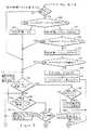
【実施例】
I.固体ディスクの概要
図1は、パーソナルコンピュータ50をブロック線図の形で示す。パーソナルコンピュータ50は中央処理装置(CPU)52と、コンピュータのユーザーに対して情報を視覚表示するモニタ54とを含む。ユーザーはキーボード56によってCPU52にデータを入力することができる。モニタ54に表示されたポインタを移動させるときには、ユーザーはマウス58を動かす。パーソナルコンピュータ50は大容量記憶のためにハード磁気ディスクではなく、本発明の固体メモリディスク60を使用する。固体ディスク60は、不揮発性半導体メモリアレイ62を制御するための固体ディスク制御装置を含む。不揮発性半導体メモリアレイ62をFLASHアレイ62ともいう。
【0012】
固体ディスク60はパーソナルコンピュータ50にいくつかの利点を与える。媒体は半導体チップであるので、大容量メモリの高さはパーソナルコンピュータ50のサイズを縮小する上でそれを制限する要因にはならなくなっている。さらに、フラッシュメモリアレイ62を形成する半導体チップは振動や衝撃の影響を相対的に受けにくく且つ電力消費も少ないので、バッテリと組合わせて使用するのに適している。従って、固体ディスク60はラップトップコンピュータ及びポータブルコンピュータで使用するのに十分に適合する。
【0013】
簡単に説明すると、本発明の固体ディスクは不揮発性半導体アレイ62の中でセクタデータを「浮動」させることによりセクタデータを記憶する。制御装置は、1つのデータのセクタを書込むための指令を受信するたびに、そのセクタの以前のバージョンをシークする。以前のバージョンを位置指定したならば、それをダーティとマークする。その後、書込むべきデータのセクタに対して、異なる記憶場所にあるメモリスペースを割当てる。最後に、割当てられたメモリにセクタデータを書込む。この方法の結果、1つの論理セクタ番号と関連するデータは固体ディスク60中の1つの固定物理記憶場所に対応しない。
【0014】
A.FLASHアレイとブロックファイル構造
固体ディスク制御装置64の制御の対象であるFLASHアレイ62を理解することは、固体ディスク制御装置64をさらに良く理解するうえで助けとなる。FLASHアレイ62のプログラム特性と消去特性は固体ディスク制御装置64に大きな影響を及ぼす。FLASHアレイ62内部のFLASHデバイスは一度に1ブロックずつ消去されなければならないが、一度に1バイトずつプログラム可能である。一旦0にプログラムされたならば、まず初めに1ブロック全体を消去しないとFLASHメモリの1ビットを1にプログラムできない。メモリの消去済バイトは書込み可能な状態となっているので、それらのバイトを「空き」という。
【0015】
FLASHメモリの消去は低速のプロセスである。データの1つのセクタを書込むたびに1回の消去を実行するのは実用的ではない。512バイトである1つのセクタを書込むだけのために128Kバイトの一対のブロックの全体を消去しなければならないので、書込みは遅くなり、また、電力消費の効率は悪くなってしまうであろう。迅速なセクタ書込みを可能にするために、1つのセクタを書込むたびに、固体ディスク制御装置64はデータの各セクタを新たな空き記憶場所に書込む。この書込み方法の結果は、1つのセクタ番号と関連してセクタデータのいくつかのバージョンが現れるということになる。セクタデータの最新のバージョンを「グッドセクタ」、「有効セクタ」又は「ユーザーセクタ」という。これに対し、セクタのそれ以前のバージョンは無効であり、「ダーティ」とマークされる。
【0016】
FLASHメモリは相対的に高価であるため、FLASHアレイ62内部のFLASHメモリの実際の量はユーザーに対して利用可能であるとして挙げられた量を大きく越えることができない。言いかえれば、FLASHアレイ62内部の予約メモリの量が不足している場合、書込みに際してのメモリの可用性を確保するために、ダーティなセクタを空きメモリに変換しなければならない。
【0017】
図2は、FLASHアレイ62と、固体ディスク制御装置64とをブロック線図の形で示す。一実施例では、FLASHアレイ62は30個の1メガバイト×8FLASHメモリチップを使用する。それらのFLASHメモリは、消去とプログラミングを自動的に制御する書込み状態機械を含む。データ圧縮を使用した場合、それらの30個のFLASHメモリデバイスは40メガバイトのメモリディスクとして機能する。各FLASHチップは一度に8ビットずつデータを入出力する。語ごとの入出力を可能にするために、FLASHアレイ62は複数対のFLASHデバイスとして編成されているのであるが、そのうち一対のチップ66のみが示されている。一対のチップ66の上位チップ68は1つの語の上位バイトを記憶し、下位チップ70は1つの語の下位バイトを記憶する。このように、固体ディスク制御装置64は各対のチップを単一の16ビット幅メモリデバイスとして扱うことができる。語ごとの入出力によって、固体ディスクドライブ60は直列ビットストリームの入出力を使用する磁気ドライブと比較して高速という利点を得ている。
【0018】
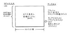
各チップ対は、それぞれが128Kバイトのメモリを含む16個のブロックとして編成されている。メモリの各ブロックは多数のデータのセクタを記憶できるので、各ブロックはデータの各セクタを識別し且つ位置指定するためのブロックセクタ変換テーブル(BSTT)84を含む。
【0019】
図3は、ブロック80と、そのブロック及び他の全てのブロックが使用するファイル構造とを示す。ブロック80は1語幅の構造として表わされているが、実際には2つのFLASHチップに記憶されている。各語の上位バイトは上位チップ68に記憶され、また、各語の下位バイトは下位チップ70に記憶されている。
ブロック80のデータ構造はブロックセクタ変換テーブル84と、データスペース86とを含む。ブロックセクタ変換テーブル84は複数の見出しを記憶している。見出しは1つの論理セクタ番号に関する情報と、その関連データとから成るブロックである。ここでいう論理セクタ番号(LSN)はBSTTの中に記憶されているセクタ番号を指す。セクタ番号はCPU52から受信したセクタ識別子であり、CPUはそのセクタ識別子が1つの固定物理記憶場所に対応するものと考える。ところが、固体ディスク60が使用する書込み方式のために、LSNは1つの固定物理記憶場所に対応しない。同様に、固体ディスクで使用する書込み方式のために、いくつかの見出しとLSNが単一のセクタ番号に対応することもあるだろう。
一実施例では、各々の論理セクタ番号は24ビットの長さである。
【0020】
ディスクをフォーマットする間、セクタ番号ごとに1つの見出しを作成する。これにより、読取り指令及び書込み指令の実行中にデータのセクタの損失を検出できる。特定の1つのセクタ番号と関連する見出しを見出せないとき、それに関連するデータのセクタが失われてしまったことがわかる。ここでいう「損失」は、FLASHアレイ62の欠陥のために消滅するデータのセクタ、又は汚れてしまったために信頼性を失ったデータのセクタを表わす。
【0021】
各々の見出し85は周期冗長検査(CRC)を含み、それにより、固体ディスク60は見出し85の信頼性を判定できる。
見出し85は、その見出しと関連するセクタデータに関する大量の情報を含む属性語を含んでいる。属性語の中の1つのビットは、セクタ番号が不良トラックの一部としてマークされているか否かを指示する。別のビットは、セクタデータが圧縮されているか否かを指示する。属性語は信頼性に関わる2つのダーティビットを含む。その双方のダーティビットがセットされていれば、見出しと関連するセクタデータは有効であると考え、いずれかのダーティビットがリセットされていれば、ダーティであると考える。属性語はデータ付加ビットをさらに含む。見出しにセクタデータが付加されていない場合、データ付加ビットはリセットされる。これは、フォーマットした後のあらゆる見出しに当てはまる。セクタ番号に関してデータが書込まれたならば、データ付加ビットはセットされる。属性語に含まれている最後の情報は改訂番号である。この改訂番号によって、固体ディスク制御装置64は、同一のLSNをもつ複数の有効見出しが存在しているときに有効見出しを識別できるのである。
【0022】
見出し85に記憶されている最後の情報はブロックセクタオフセット(BSO)である。BSOは見出しと関連するFLASHメモリスペースの始めに対するブロックの最上部からのオフセットである。メモリスペースにデータが記憶されていても、いなくても、そのメモリスペースは1つの見出しに割当てられる。データが見出しに付加されていなければ、割当てられるメモリの量はデータスペース86のサイズをBSTT84における見出しの最大数で除算したものである。
【0023】
メモリスペースは、セクタデータが付加されていない見出しに割り当てられなければならない。これは、フォーマットする間にBSTT84の全てがデータ付加のない見出しで充填されているためである。それらのBSTT84と関連するデータスペース86の全体が空いているとしても、データスペース86に書込むことは不可能である。これは、単に、それらのブロックのBSTTに余地がないためである。割当てのために空きメモリを利用できないキャッチ22状況を回避するために、それらのBSTT84と関連するデータスペース86の全てはユーザーデータとして分類される。言いかえれば、セクタはダーティビットにより指示されるようにダーティでもなく、空きでもないということになる。データが付加されていない見出しにメモリデータスペース86を割当て且つそのメモリの量を適切なブロック、適切なチップ及びアレイにある空きメモリの量から減じることにより、データスペース86の一部がユーザーデータとして指定される。フォーマットした後にデータのセクタを書込んでゆく間に、データが付加されていない見出しはその割当てられたデータスペースと共にダーティとマークされる。最終的に、フォーマットした間に充填されたブロックはクリーンアップされて、そのデータスペースは空きメモリとして利用可能になる。
【0024】
データ圧縮を使用しない場合、データを付加せずに見出しを書込みできることは重大である。データ圧縮を使用しないときには、クリーンアップのために利用可能である予約はほとんどなく、起こりうるデータのセクタごとに全て固体ディスク60に書込むことになる。この状況ではクリーンアップ効率はひどく損なわれてしまい、データの断片化が生じるおそれがある。このデータ断片化は今度は数多くのフォアグラウンドクリーンアップをもたらし、固体ディスク全体の性能を劣化させる。
【0025】
データスペース86で1つのセクタに関わるデータが別のセクタに関わるデータとぶつかり合うので、各々のBSOは1つのセクタに関わるデータの最上位部分と、別のセクタに関わるデータの最下位部分とを指示する。たとえば、セクタ1のブロックオフセットであるBSO1 はLSN1 と関連するデータの始まりを指示する。BSO1 はLSN2 と関連するデータの最下位部分をも指示する。ブロックセクタ変換テーブル84を見る別の方法は、各々のLSNが2つのブロックセクタオフセットの間にはさまれており、その一方のブロックセクタオフセットはセクタデータの最上位部分を指示し、他方はセクタデータの最下位部分を指示するというものである。ブロックの最下位部分に記憶されているセクタLSN1 と関連するデータの最下位部分は、ブロックの最下位部分の場所がわかっているために、BSOにより指示されなくとも良い。
【0026】
ブロックセクタ変換テーブル84はデータスペース86に向かって下方へ成長してゆく。第1の見出しBSTT84はブロック80の最上位部分に書込まれる。ブロック80に書込まれる後続する各セクタに関わる見出しは、先の見出しの下方に記憶される。
【0027】
BSTT84とは対照的に、データスペース86は上方へ成長する。ブロック80に書込まれるデータの第1のセクタはデータスペース86の最下位部分に書込まれる。データスペース86に書込まれるデータの次のセクタは先のセクタのすぐ上方に書込まれる。たとえば、LSN2 と関連するデータはLSN1 と関連するデータより低いアドレス範囲の中に位置している。
【0028】
データスペース86に記憶しうるセクタの数は、BSTT84に入り込む前に変動する。この可変性は、セクタデータが圧縮されているときにセクタのサイズが変動するために起こる。データ圧縮を伴うとき、セクタのサイズは256語からわずか数語まで変わると思われる。固体ディスク60がシーク戦略を使用するとすれば、最大限2047個のセクタをデータスペース86に記憶できるであろう。
【0029】
固体ディスク制御装置64はBSTT84とデータスペース86が成長してゆく間に互いにぶつかり合うのを防止する。実際には、固体ディスク制御装置64はBSTT84とデータスペース86との間に幾分かのスラック88が維持されるように保証する。スラック88は、まだプログラムされていない空きFLASHメモリである。FLASHメモリの規約に従えば、空いた記憶場所はFFFF(16進数)を記憶する。ブロックセクタ変換テーブル84のシーク中、スラック88はBSTT84の終わりに到達したことを指示する。
【0030】
ブロック80はブロック属性データ90をさらに記憶している。そのブロックに特有の情報が記憶される属性データ90である。たとえば、ブロック属性データ90は、ブロックが消去されて、そのブロックに書込んだ回数を指示するサイクルカウントを含む。ブロック属性データ90はブロック欠陥情報を含んでいても良い。
【0031】
B.固体ディスク制御装置ハードウェアの概念
再び図2を参照して説明すると、FLASHアレイ62の読取り、書込み及びクリーンアップは固体ディスク制御装置64により制御される。マイクロプロセッサ92はデータベース93と、セクタ見出し変換テーブル(SHTT)94と、FLASHメモリ95に記憶されている本発明のアルゴリズムとを使用してそれらのタスクを管理する。データベース93、SHTT94及びアルゴリズムについては以下にさらに詳細に説明する。アプリケーション特定集積回路であるウィンドウASIC96は、マイクロプロセッサ92の外界に対するウィンドウ並びにFLASHアレイ62に対するウィンドウとして機能する。ウィンドウASIC96を介してマイクロプロセッサ92はCPU52から指令を受信すると共に、FLASHアレイ62に対する読取りと書込みを実行する。言いかえれば、ウィンドウASIC96はマイクロプロセッサ92のアドレス可能メモリスペースを増加させる。ウィンドウASIC96は4つのウィンドウを含むので、マイクロプロセッサ92はいくつかのFLASH記憶場所を繰り返し、急速にアクセスできる。データは、CPU52との間で、ウィンドウASIC96を介して流れて、セクタバッファ98に至る。セクタバッファ98があるために、CPU52に向かうデータの転送はセクタバッファがない場合に可能であるよりも急速に起こりうる。固体ディスク制御装置64は電荷ポンプ100を含む。電荷ポンプ100は5ボルトをプログラミングと消去に必要とされる12ボルトレベルに変換する。固体ディスク60に供給される電圧レベルがFLASHアレイ62の中のFLASHデバイスをプログラムするために必要な12ボルト電圧レベルより全て低くならない限り、電荷ポンプ100は必要ではない。
【0032】
C.FLASHアレイデータベースとセクタ見出し変換テーブル
繰り返し使用される情報をランダムアクセスメモリ(RAM)に記憶することにより、固体ディスク60の性能は向上する。この情報は、一般に、FLASHアレイ62の現在特性に関連しているので、これをFLASHアレイデータベース93という。FLASHアレイデータベース93の中の情報は、
1.FLASHアレイ62内部のダーティな語の総数(TDFA);
2.各ブロック内部のダーティな語の総数(TDFBN);
3.FLASHアレイ62内部の空きの語の総数(TFFA);
4.各チップ対の中の空きの語の数(TFFCM) ;
5.各ブロック内部の空きの語の総数(TFFBN)
を含む。
【0033】
固体ディスク制御装置64がFLASHアレイデータベース93をどう使用するかを以下にアルゴリズムごとに説明する。
セクタ見出し変換テーブル(SHTT)94はセクタ番号を関連するデータのセクタに対するポインタに変換する。SHTT94を頻繁且つ容易に変更できるように、SHTT94をRAMに記憶しておくのが好ましい。セクタ見出し変換テーブル94は、与えられたセクタ番号と関連するデータを直接には指示しない。そうではなく、SHTT94により供給されるポインタはBSTT84の中、そのセクタ番号と関連する見出しの付近の記憶場所を指示する。
【0034】
SHTT94がセクタ番号と関連する見出しを直接には指示しない理由を理解するには、BSTT84に現れうる見出しをそれぞれ一意性をもってアドレス指定するために必要なビットの数を考えてみれば良い。BSTT84には、最大限2047個の見出しを記憶できる。チップが15対あり、一対のチップにそれぞれ16のブロックが含まれているものとすれば、FLASHアレイ62は491,280個の見出しを記憶することができるであろう。それほど多くの見出しを一意性をもって識別するには19ビットが必要である。19ビットを記憶するには、3×8個のRAMチップを使用しなければならない。従って、3つのビットを記憶するために、1つのRAMにおける8ビットのうち5つが浪費されるであろう。これは、競合しうる価格の固体メモリディスクを製造しようとする努力の中では高価で、受け入れられない解決方法である。
【0035】
この19ビットのジレンマを解決するSHTTのデザインはいくつかある。図4に示す一実施例では、工業規格の40MBディスクドライブのデータの数の現れうる83300個のセクタの各々に対して1つずつのポインタを記憶する。SHTT94の各エントリには16ビットしか記憶されていない。それらのビットのうち4つは、シーク中のセクタデータを記憶しているチップ対を指示する。もう4つのビットはそのセクタを記憶している特定のブロックを指示する。残る8つのビットは、所望の見出しの付近にある見出しに対するブロックの最上位部分からのオフセットを表わす。このオフセットを見出しポインタと呼ぶ。見出しポインタを表わすために8ビットを使用するということは、最大限2047個の見出しを位置指定するために256個の見出しポインタを利用できることを意味している。そこで、所望の見出しを位置指定するためには、BSTT84において最大で8個の見出しを走査しなければならない。言いかえれば、SHTT94aは1つの特定のセクタ番号と関連するデータを位置指定するために2段の探索を要求するということがある。まず、特定のチップ、ブロック及び見出しポインタを位置指定するためにSHTT94aを探索する。第2に、セクタ番号と関連する見出しを見出すために、BSTT84の指示領域を探索する。
【0036】
図4のSHTT94は固体ディスク60に記憶されているセクタごとに1つの物理アドレスを記憶する。最新のキャッシュメモリを使用することにより、SHTT94のエントリの数を減少できる。
【0037】
FLASHアレイデータベース93とSHTT94は不揮発性メモリであるRAMに記憶されること、及び読取りと書込みがデータベース93とSHTT94に縦続して実行されることを理由として、パワーアップ中にFLASHアレイデータベース93とSHTT94の双方を生成しなければならない。図5は、FLASHアレイデータベース93とSHTT94の双方を作成するためのアルゴリズムを示す。このアルゴリズムを使用すると、SHTT94とFLASHアレイデータベース93は、共に、各々のBSTT84を走査することにより生成される。各セクタ番号と関連する見出しの記憶場所と、ブロック中の空きメモリとダーティメモリの量とに注目する。
【0038】
作成はステップ110においてSHTT94の初期設定と共に始まる。セクタ番号ごとの各ポインタを同じ初期値に設定する。一実施例では、その値はFFFF(16進数)である。そのため、SHTT94を作成した後に初期値と等しいポインタを検索すると、フォーマットする間にセクタ番号ごとに1つの見出しが作成されていることから、そのセクタ番号と関連するデータのセクタが失われてしまっていることがわかる。マイクロプロセッサ92はステップ110からステップ111へ分岐する。
【0039】
ステップ111では、FLASHアレイ中の空きメモリの総量であるTFFAと、チップごとの空きメモリの総量であるTFFCM とをその最大値に初期設定する。チップごとの最大空きFLASHは64Kバイト/ブロック* 16ブロック、すなわち、チップ対ごとに2048バイトから各ブロックに記憶されているブロック属性データを減じたものである。同様に、TTFAmax はチップ対ごとに2048Kバイト* 15チップ対、すなわち、約30Mバイトである。これを実行したならば、マイクロプロセッサ92はステップ112へ分岐して、BSTT84を走査し始める。
【0040】
ステップ112では、マイクロプロセッサ92はFLASHアレイ62に今後に走査すべきブロックが残っているか否かを判定する。残っていれば、マイクロプロセッサ92はステップ114へ進み、走査すべきブロックBC を選択する。マイクロプロセッサ92はステップ114からステップ115へ分岐する。そこで、現在ブロックの空きメモリの総量TFFBC をその最大値に初期設定する。マイクロプロセッサ92は、次に、ステップ116に進む。
ステップ116では、マイクロプロセッサ92は選択したブロックのブロックセクタ変換テーブル84から次の見出しを読取る。その後、マイクロプロセッサ92はステップ118へ分岐する。
【0041】
マイクロプロセッサ92はステップ118で現在見出しを分類し始める。マイクロプロセッサ92は、現在見出しの属性語に含まれているダーティビットを読取ることにより、見出しがダーティとマークされているか否かを判定する。いずれかのダーティビットが論理値0であれば、LSNと関連するデータはダーティであると考える。データのセクタがダーティであれば、マイクロプロセッサ92はステップ120へ分岐して、FLASHアレイデータベース93を更新する。
【0042】
ステップ120では、マイクロプロセッサ92はダーティセクタのサイズを確定するのであるが、そのサイズはデータ圧縮の結果として変わることもある。セクタのサイズは現在LSNの両側のブロックセクタオフセットを比較することにより確定される。ダーティセクタのサイズを確定した後、マイクロプロセッサ92はTDFAとTDFBC を更新する。ダーティな語の総数であるTDFAと、現在ブロックの中のダーティな語の総数であるTDFBC とをセクタとその見出しのサイズだけ増加させるのである。その後、マイクロプロセッサ92はステップ121へ進む。
マイクロプロセッサ92はそのFLASH空き変数を適切に改訂する。現在セクタとその見出しのサイズをTFFA、TFFBC 及びTFFCC から減じる。その後、マイクロプロセッサはステップ116に戻ることにより、FLASHアレイデータベース93とSHTT94の作成を再開する。
【0043】
これに対し、セクタがダーティでない場合には、マイクロプロセッサ92はステップ118からステップ122へ分岐する。そこで、マイクロプロセッサ92は、BSTT84の終わりに達したか否かを判定するために、現在見出しの中の属性語を検査する。次の見出しに関わる属性語がFFFF(16進数)であるならば、終わりに達している。この場合、マイクロプロセッサ92はステップ112に戻って、BSTT84の走査を継続すべきか否かを判定する。他のあらゆるケースにおいては、マイクロプロセッサ92はステップ122からステップ124に進む。
【0044】
ステップ124に入るということは、現在見出しがユーザーデータの有効セクタと関連していることを意味している。従って、マイクロプロセッサ92は空き変数TFFA、TFFBC 及びTFFCC を現在セクタのサイズだけ減少させる。(添字「C」は「現在」を指示している。)これを実行したならば、マイクロプロセッサ92はステップ126へ進む。
【0045】
ステップ126では、現在見出しに含まれているLSNと等しいセクタ番号を求めてSHTT94のエントリをシークすることにより、現在見出しに関わるSHTTエントリの改訂を開始する。SHTTの現在エントリがFFFF(16進数)であれば、そのセクタ番号に関わる情報は存在していない。マイクロプロセッサ92はステップ128へ分岐することによりこれに対応する。セクタ番号に関わるエントリがFFFF以外であれば、いずれの場合にも、そのセクタ番号に関してデータの2つの有効バージョンがあるということになる。物事を分類するために、マイクロプロセッサ92はステップ130へ進む。
【0046】
まず、より単純な状況、すなわち、現在LSNに対応するセクタ番号に関わるデータがSHTT94に記憶されていない場合を考える。ステップ128では、マイクロプロセッサ92は現在見出しに関わるチップ、ブロック及び見出しポインタをSHTT94に書込む。これを実行したならば、マイクロプロセッサ92はステップ116に戻って、別の見出しを検査する。
【0047】
SHTT94が現在LSNと関連するセクタ番号に関わるエントリを既に含んでいる場合には、状況はさらに複雑になる。ステップ130では、マイクロプロセッサは改訂番号を比較することによりどの見出しが、従って、どのデータのセクタが最も新しいかを判定する。次のステップ132では、マイクロプロセッサ92は先のダーティビットを論理値0にプログラムすることにより、そのデータの先の無効セクタをダーティとマークする。
【0048】
ステップ133では、直前にダーティであるとマークされたセクタを含むブロックと、FLASHアレイ62とに関わる総ダーティを反映するために、マイクロプロセッサはデータベース93を更新する。その更新は、セクタのサイズをTDFBC 及びTDFAに加算することにより実行される。
【0049】
ステップ134では、必要に応じて、SHTT94を最終的に更新する。見出しとステップ116で選択したLSNがステップ132でダーティとマークされていれば、更新は不要である。そうでなければ、ステップ116で選択したLSNに関わるチップ、ブロック及び見出しポインタをSHTT94に書込む。
【0050】
マイクロプロセッサ92はステップ134からステップ116に戻る。そこで、別の見出しを選択する。
FLASHアレイ62内部の見出しを走査し終わるたびに、SHTT94の作成は完了する。1つのセクタ番号に対応する見出しが位置指定されていなければ、SHTT94の中のポインタは初期値にとどまる。すなわち、ポインタはデータのセクタが失われたことを指示し、SHTT94はどのデータのセクタをも考慮に入れているのである。
【0051】
II.固体ディスク制御装置
固体ディスク制御装置64の心臓部は、FLASHメモリ95の中に記憶されている1組のアルゴリズムである。それらのアルゴリズムはFLASHアレイ62の読取り、書込み及びクリーンアップを制御する。それらのアルゴリズムは、CPU52が工業規格のハード磁気ディスクドライブを取り扱っているかのような錯覚を作り出すのを助ける。
【0052】
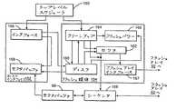
図6のオブジェクト線図は、固体ディスク制御装置64が使用するアルゴリズムの総体的な編成と相互関係を示す。固体ディスク制御装置64のアルゴリズムはトップレベルスケジューラ150、ホストインタフェース152、そして、FLASH媒体154という3つのクラスに編成されている。トップレベルスケジューラ150は他の2つのクラス152及び154の間でのCPU92の処理時間の割当てを処理する。ホストインタフェース152はCPU52からの工業規格ディスクドライブ指令を解釈し、それらをFLASH媒体154が反応しうる指令に変換する。FLASH媒体154はFLASHアレイ62と直接にインタフェースし、ホストインタフェース152からの読取りと書込みの要求に応答する。FLASH媒体154はFLASHアレイ62のクリーンアップをも管理する。
【0053】
ホストインタフェース152とFLASH媒体154のスケジューリングは相対的に単純なタスクである。固体ディスク60のパワーアップはトップレベルスケジューラ150を始動する。スケジューラは固体ディスク60を初期設定し、次に、ホストインタフェース152を呼び出す。これはCPU52に固体ディスク60のあらゆる資源を割当てる。ホストインタフェース152がトップレベルスケジューラ150に制御を戻したとき、クリーンアップオブジェクト164が呼び出される。クリーンアップが進行中である場合、クリーンアップにはCPU実行時間の1スライス、一実施例では500μ秒が割当てられる。クリーンアップがトップレベルスケジューラ150に制御を戻すと、ホストインタフェース152が再び呼び出される。固体ディスク60がパワーアップされている間は、トップレベルスケジューラ150はそのプロセスを何度も繰り返す。
【0054】
ホストインタフェース152はインタフェース156及びセクタバッファ158という2つのクラスのアルゴリズムを含む。インタフェース156はAT−IDEハードディスクインタフェースをエミュレートする。インタフェース156はATA指令割込みを処理し、ATA指令をFLASH媒体154により理解可能な指令に変換する。別の実施例においては、ホストインタフェース156はSCSIディスクインタフェース又は他の規格によるディスクドライブインタフェースをシミュレートしても良い。セクタバッファ158はセクタバッファ98の使用を管理する。
【0055】
簡単に説明すれば、FLASH媒体154は5種類のアルゴリズム、すなわち、ディスク160、セクタ162、クリーンアップ164、FLASHパワー166及びFLASHアレイインタフェース167という5つのサービスを含んでいることになる。ディスク160はインタフェース156からの読取り要求と書込み要求をサービスする。また、ディスク160はディスク160からの他の指令を変換し、それらを他のクラス162、164、166及び167に移して実行させる。セクタ162はFLASHアレイ62内部に記憶されているセクタに関連する大部分のタスクを実行する。セクタ162はディスク160とクリーンアップ164の双方により使用されるFLASHアレイデータベース93を維持すると共に、FLASHアレイ62の中の空きメモリスペースを割当てる。さらに、セクタ162はFLASHアレイ62からのデータの読取りをFLASHアレイインタフェース167と、シーケンサ168とを介して制御する。FLASHパワー166は本質的にはデバイスドライバである。すなわち、FLASHパワーはFLASHアレイ62に対する読取り又は書込みに必要な電圧レベルを発生するのである。FLASHアレイインタフェース167は、FLASH62の読取りと書込みを直接に制御する低レベルルーチンを処理する。シーケンサ168はセクタバッファ98と、FLASHアレイ62との間のデータの移動を処理する。クリーンアップ164は、その名が示す通り、FLASHアレイ62のクリーンアップを管理する。FLASHパワー166は固体ディスク60の限定された予定電流を管理するのであるが、一実施例では、この電流はわずか120mAである。一対のチップで1つのブロックを消去するのに60mAまでが必要であるとすれば、電流の効率の良い管理は重要である。
【0056】
A.FLASHアレイからのセクタの読取り
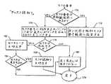
簡単に説明すれば、1つのセクタの読取りは3段階のプロセスである。まず初めに、セクタ番号と関連する見出しに対するポインタを求めてSHTT94を探索する。第2に、見出しを位置指定し、その属性語を検査して、付加データが有効であるか否かを知る。第3に、見出しと関連するセクタデータが有効であれば、その記憶場所を確定し、CPU52に戻す。
ディスク160により実現される読取りアルゴリズムを図7の流れ図に示す。全ての呼び出し側はセクタ番号を入力する。
【0057】
ステップ170におけるマイクロプロセッサ92の最初のタスクは、有効性に関わる入力セクタ番号の検査である。工業規格によるディスクドライブの中にあるセクタの最大数で、セクタ番号が有効であるか否かを判定する。たとえば、規格の40MBドライブは83300個のセクタを含む。従って、40MBドライブの場合、83300を越えるセクタ番号はいずれも無効になるであろう。
【0058】
呼び出し側プログラムが無効セクタ番号を与えていた場合、マイクロプロセッサ92はステップ170からステップ172へ分岐する。マイクロプロセッサ92は、状態語を無効セクタ番号範囲に設定することにより、セクタ番号の無効性を呼び出し側に指示する。次に、マイクロプロセッサ92はステップ174に戻り、制御を呼び出し側に戻す。
【0059】
これに対し、呼び出し側が有効セクタ番号をもつセクタを読取ることを要求した場合には、マイクロプロセッサ92はステップ170からステップ176へ進む。ステップ176では、マイクロプロセッサ92はセクタ番号を取り上げ、セクタ番号と関連するチップ、ブロック及び見出しポインタを求めてSHTT94を探索する。
【0060】
ステップ178では、マイクロプロセッサ92は要求されたセクタ番号に関わるデータが存在するか否かを判定する。マイクロプロセッサ92は、SHTT94から検索した見出しポインタを検査することにより、特定のセクタ番号について見出しが存在するか否かを報知することができても良い。見出しポインタがFFFF(16進数)である場合、フォーマットする間にセクタ番号ごとに1つの見出しを作成していても、セクタ番号に対して有効見出しを見出すのは不可能である。
マイクロプロセッサ92は、ステップ178からステップ180へ分岐することにより損失セクタに応答する。そこで、マイクロプロセッサ92は見出しを見出せなかったことを指示する。次に、マイクロプロセッサ92はステップ174へ分岐して、読取りは完了する。
【0061】
これに対し、セクタ番号に対する見出しが存在しているのであれば、マイクロプロセッサ92はステップ182へ分岐する。そこで、セクタ162は入力されたセクタ番号と関連する見出しをシークする。所望の見出しを位置指定したならば、セクタ162はチップ、ブロック及びその見出しに対するオフセットを指示する。セクタ162は、所望の見出しを見出せない場合にも指示する。
【0062】
セクタ162がそのシークから復帰したならば、マイクロプロセッサ92はステップ184へ分岐して、シークの成否を判定する。シークアルゴリズムがセクタ番号と関連する見出しを位置指定しなかった場合には、マイクロプロセッサ92はステップ180へ分岐して、そのことを呼び出し側に報知する。これに対し、適切な見出しが位置指定されたならば、マイクロプロセッサ92はステップ186へ分岐する。そこで、ステップ182で検索した情報をセクタオブジェクト162の読取りサービスにパスする。セクタ番号と関連するデータをセクタバッファ98にコピーし且つホストCPU52に供給する。その後、読取りが完了して、マイクロプロセッサ92はステップ174へ分岐することにより制御を呼び出し側に戻す。
【0063】
図8は、セクタ番号が与えられたときにセクタデータをシークする方法を示す。このアルゴリズムもセクタ162により実現される。
簡単に説明すれば、図8のシークアルゴリズムはセクタ番号と関連するデータを位置指定する2つの方式を有する。第1の方式は、シーク時間を短縮するためにデータのコヒーレンシーに依存する。すなわち、現在シーク中であるデータのセクタは最前に位置指定されたデータのセクタに関連しており且つその付近に位置しているものと仮定する。この方式が、所望のデータのセクタを位置指定しそこなえば、次に2段階方式が使われる。まず、セクタ番号入力SNi に関わるチップ、ブロック及び見出しオフセットを位置指定するために、SHTT94を探索する。次に、その情報を使用して、呼び出し側により入力されたセクタ番号と等しいLSNをもつ見出しを求めてBSTT84を探索する。
【0064】
データのセクタの位置指定はステップ190で始まる。そこで、マイクロプロセッサ92は、探索した最前のBSTT84に別の見出しが記憶されているか否かを判定する。記憶されていれば、入力セクタ番号と関連する見出しが同じBSTT84の中にある可能性がある。その場合、マイクロプロセッサ92はステップ192へ進む。しかしながら、最前に位置指定した見出しがそのBSTT84の中で最後に位置指定した見出しであった場合には、入力セクタ番号と関連するデータのセクタを急速に位置指定することは可能ではない。二段階探索を使用しなければならない。その場合には、マイクロプロセッサ92はステップ206へ進み、その二段階探索を開始する。
【0065】
まず、ステップ192に入るときのマイクロプロセッサ92のアクションについて考える。マイクロプロセッサ92は、最前に位置指定した見出しのすぐ次に続く見出しを読取る。この見出しの中のLSNを「LSNL+1」 と指定する。LSNL+1 をステップ194のSNi と比較して、現在見出しが所望の見出しであるか否かを判定する。LSNL+1 がSNi と等しくなければ、別の方法でデータのセクタを位置指定しなければならない。その場合には、マイクロプロセッサ92はステップ206へ進む。これに対し、LSNL+1 がSNi と等しい場合には、マイクロプロセッサ92はステップ196へ分岐する。
【0066】
現在見出しの信頼性を確定するプロセスはステップ196をもって始まる。ステップ196の間、マイクロプロセッサは現在見出しに関わる周期冗長検査(CRC)を生成する。このCRCを「CRCG」 と呼ぶ。ステップ198では、CRCG を見出し自体に記憶されているCRCであるCRCstoredと比較する。CRCG =CRCstoredであるとき、現在見出しの中の情報を信頼しうるものと考える。マイクロプロセッサ92はステップ202へ分岐することによりこの状態に応答する。これに対して、CRCstoredと等しくないために現在見出しが信頼できない場合には、マイクロプロセッサ92はステップ206へ進む。
【0067】
まず、所望の見出しを位置指定したときのマイクロプロセッサ92のアクションを考える。マイクロプロセッサ92は、第1に、ステップ200で見出しと関連するデータのセクタのサイズを確定する。これは、先に説明した通り、適切なブロックセクタオフセットを使用して実行される。ステップ202では、セクタのサイズ、チップ、ブロック及び所望の見出しに対するオフセットを呼び出し側に戻す。
これが成功すれば、ステップ190〜202から成る方法は1つのデータのセクタを位置指定するために要する時間を、ステップ206〜222から成る二段階探索と比べて四分の一に短縮する。
【0068】
二段階探索は、より迅速な方式が失敗に終わった後にステップ206から始まる。マイクロプロセッサ92は、セクタ番号入力SNi と関連するチップ、ブロック及び見出しポインタを求めてSHTT94をシークすることにより第1レベルの探索を実行する。ステップ206で検索したチップ、ブロック及び見出しポインタの値をステップ208で検査して、SNi について見出しを位置指定することが可能であるか否かを判定する。それらの値が初期値と等しいならば、SNi と関連する見出しは失われていることになる。一実施例では、初期無効値はFFFF(16進数)である。マイクロプロセッサ92は、ステップ224へ分岐することにより、無効のチップ、ブロック及び見出しポインタの値に応答する。そこで、入力セクタ番号と関連する見出しが見出されなかったことを呼び出し側に報知する。これに対し、SHTT94から検索した値が有効である場合には、マイクロプロセッサ92はステップ210へ進む。
【0069】
シークの第2の段階は、ステップ210で、走査カウントを零に初期設定することによって始まる。走査カウントはシーク中に検査される見出しの番号を追跡する。そこで、マイクロプロセッサ92は見出しポインタの付近の見出しを読取る。
マイクロプロセッサ92はステップ210からステップ208へ進んで、現在走査カウントを最大走査がカウントと比較する。
【0070】
走査しなければならない見出しの最大数は、BSTT84中の見出しの最大数を見出しポインタの最大数で除算することにより設定される。たとえば、固定ディスク60の一実施例では、BSTT84に記憶される見出しの最大数は2047であり、使用する見出しポインタの数は256のみである。従って、この実施例では8つまでの見出しを走査しなければならない。走査カウントが最大値より小さいならば、マイクロプロセッサ92はステップ212へ分岐して、所望の見出しの探索を継続する。これに対し、走査カウントが最大値を越えたならば、マイクロプロセッサ92はステップ200からステップ224へ進む。
【0071】
まず、走査カウントが最大値より小さいときの状況を考える。マイクロプロセッサ92はステップ214に入り、現在見出しの中に記憶されているLSNを入力セクタ番号と比較する。それら2つが等しいならば、所望の見出しは位置指定されていることになるであろう。そうでなければ、所望のセクタを求める探索を継続しなければならない。
ステップ222では、走査カウンタを増分し且つ最前の見出しの下方に位置する別の見出しを読取ることにより、所望のセクタの探索を継続する。そこで、マイクロプロセッサ92はステップ212に戻り、この新たな見出しが所望の見出しであるか否かを判定する。
【0072】
LSNが入力セクタ番号と等しいとき、マイクロプロセッサ92はステップ214からステップ216へ進む。ステップ216では、現在見出しについて周期冗長検査CRCG を生成する。ステップ218では、CRCG を使用して、見出しに含まれている情報の信頼性をアクセスする。
そこで、マイクロプロセッサ92は、セクタ番号SNi をブロックに記憶されているLSNと比較することにより、現在見出しがシーク中の見出しであるか否かを判定する。LSN=SNi であれば、マイクロプロセッサ92はステップ216へ進む。
ステップ218では、CRCG を選択した見出しに記憶されているCRCと比較することにより見出しの信頼性を確定する。2つのCRCが等しくない限り、見出しの中の情報を信頼することはできない。
【0073】
現在見出しが信頼できるものではないならば、マイクロプロセッサ92はステップ218からステップ220へ分岐する。現在見出しの中のブロックセクタオフセットを信頼することができないので、2つのデータのセクタは失われる。たとえば、図3に示すように、走査中の見出しがLSN1 に関わる見出しであったと仮定する。BSO1 を信頼できないので、LSN1 に関わるデータの始まりも、LSN2 に関わるデータの終わりも共に確定することができない。従って、ステップ220では、マイクロプロセッサ92は選択した見出しと、そのすぐ下方にある見出しの双方をダーティにすることにより、2つのデータのセクタを放棄する。次に、マイクロプロセッサ92はステップ222へ進む。
【0074】
現在見出しを信頼できる場合には、マイクロプロセッサ92はステップ218からステップ220へ進む。ステップ206に達したならば、マイクロプロセッサ92はセクタデータを読取るために必要とされる情報を収集し始める。まず、適切なBSOを読取ることによりセクタのサイズを確定する。最後に、ステップ202では、セクタのサイズ及び属性語をチップ、ブロック及び見出しに対するオフセットと共に呼び出し側に戻す。次に、マイクロプロセッサ92はステップ204で制御を呼び出し側に戻す。
【0075】
B.FLASHアレイ62へのセクタの書込み
1つのデータのセクタの書込みは3つの主要なタスクを含む。第1に、そのセクタデータを書込むのに十分な空きメモリを位置指定し且つ予約しなければならない。第2に、同じLSNの中にセクタデータの先のバージョンがあれば、それをダーティとマークし、セクタ見出し変換テーブル94を更新する。第3に、セクタデータとその見出しを適切なブロックに書込む。
【0076】
図9は、1つのデータのセクタをFLASHアレイ62に書込むプロセスの概要を提示している。書込みは、ディスク160がCPU52から入力セクタ番号SNi を伴う書込み指令を受信したときに始まる。この時点で、FLASHアレイ62に書込むべきデータはセクタバッファ98の中にある。LSNi 及びSHTT94に記憶されているデータに従って図10のアルゴリズムを使用すると、いくつかの結果が起こりうる。
【0077】
まず初めに、SNi が無効であるときの結果を考える。書込み指令を受信したときのマイクロプロセッサ92の第1のアクションは、SNi を検査することである。これはステップ230で実行される。83300より大きいSNi 又は1より小さいSNi は、いずれも、40MBドライブには書込まれない。
【0078】
SNiが無効であるとすれば、マイクロプロセッサ92はステップ230からステップ232へ分岐する。そこで、受信したセクタ番号が無効であったことをインタフェース156に報知するために、マイクロプロセッサ92は状態語をセットする。これを実行した後、マイクロプロセッサ92はステップ234へ進む。次に、マイクロプロセッサ92の制御は呼び出し側プログラムに戻る。
今度は、SNi が有効であり且つその属性語はSNi と関連するトラックが不良とマークされたことを指示しているものと仮定する。SNi は有効であるので、マイクロプロセッサ92はステップ230からステップ236へ分岐する。
【0079】
セクタを書込むための準備はステップ236で本格的に始まる。マイクロプロセッサ92は電荷ポンプ100をイネーブルし、電荷ポンプ100にFLASHメモリをプログラムするために必要な12ボルトのレベルを発生させることができる。そこで、マイクロプロセッサ92は電荷ポンプ100が12ボルトに達するまで他のタスクを実行する。
【0080】
ステップ238では、マイクロプロセッサ92は、セクタデータのより以前のバージョンを求めて、チップ、ブロック及び見出しポインタを位置指定するためのシークアルゴリズムを呼び出す。セクタ番号と関連する情報を位置指定した後、マイクロプロセッサ92はステップ240へ分岐する。
ステップ240では、マイクロプロセッサ92は不良トラックビットがセットされているか否かを判定する。マイクロプロセッサ92はセクタ属性語を検査することによりこれを実行する。不良トラックビットが表明されていたならば、マイクロプロセッサ92はステップ240からステップ242へ進む。
【0081】
SNi と関連するトラックが不良であるとマークされているので、マイクロプロセッサ92はセクタデータをFLASHアレイ62に書込まない。ステップ242では、マイクロプロセッサ92はトラックが不良であることをインタフェース156に報知する。その後、マイクロプロセッサ92はステップ234へ分岐することにより制御をインタフェース156に戻す。
先の説明からわかるように、SNi が無効であるか又はそれに関連するトラックが不良であるとマークされていたかのいずれかの場合には、データのセクタはFLASHアレイ62に書込まれない。逆にいえば、セクタデータが良いトラック及び有効なSNi と関連しているならば、そのセクタデータはFLASHアレイ62に書込まれることになる。次に、そのような状況について考えてみる。マイクロプロセッサ92はステップ238からステップ244へ分岐することにより応答する。
【0082】
ステップ244では、マイクロプロセッサ92は電荷ポンプ100が12ボルトに達したか否かを判定するために、電荷ポンプ100に絶えず問合わせる。電荷ポンプ100が12ボルトに達するのに要する時間の量は、電荷ポンプ100が最後にイネーブルされてからどれほどの時間が経過しているかによって異なるので、予測不可能である。電荷ポンプ100が始動して以来の時間が長いほど、12ボルトに再び達するために要する時間は短くなる。電荷ポンプ100が12ボルトで安定したならば、マイクロプロセッサ92はステップ246へ分岐する。
【0083】
ステップ246では、マイクロプロセッサ92は同じLSNをもつ以前の見出しをダーティとマークすべきか否かを判定する。マイクロプロセッサ92は、ステップ238のシークによって検索した情報に基づいてこの判定を実行する。見出しが位置指定されていた場合、マイクロプロセッサ92はステップ247へ進み、その見出しをダーティとマークする。その後、マイクロプロセッサ92はステップ248へ進み、以前の見出しがダーティとマークされていたか否か又はタスクがキャッシュされていたか否かを判定する。タスクがキャッシュされていなければ、マイクロプロセッサ92はステップ250へ進む。キャッシュされていれば、マイクロプロセッサ92はステップ249へ分岐する。ダーティとマークすることがキャッシュされていたため、現在書込みの終わりに同じLSNをもつ2つの見出しが現れるであろう。パワー損失後に有効データを区別するために、ステップ249では、最も新しいバージョンと関連するLSNに関わる改訂番号を増分する。次に、マイクロプロセッサ92はステップ250へ進む。
【0084】
マイクロプロセッサ92は、FLASHアレイ62の中のセクタデータの新たなバージョンを書込むプロセスをステップ250をもって開始する。マイクロプロセッサ92はデータのセクタ及び見出しを記憶するのに十分な空きメモリをFLASHアレイ62の内部で割当てる。これは、以下に詳細に説明する複雑なプロセスである。ここでは、メモリの割当てには、1ブロックのデータスペース86の中に十分なメモリを位置指定し且つそのメモリスペースを予約済としてマークすることが必要であると述べるだけで十分である。次に、マイクロプロセッサ92はステップ252へ進む。
【0085】
マイクロプロセッサ92はステップ252及び254で見出しの書込みを完了する。まず、ステップ252では、見出しについてCRCを生成するのであるが、ダーティビットと改訂番号は事象の経過の中で変化することがあるので、それらは除外される。その後、ステップ254では、属性語とLSNをBSTT84に書込む。LSNをSNi と等しくなるように設定する。
マイクロプロセッサ92は最終的にはステップ256で予約したデータスペースにセクタデータを書込む。データと共に、誤り訂正コードECCをも書込む。
【0086】
セクタデータの新たなバージョンを確実に書込んだならば、ステップ258では、セクタ見出し変換テーブル94がセクタ番号と関連するセクタデータの最も新しいバージョンを指示するように、マイクロプロセッサ92はセクタ見出し変換テーブル94を更新する。
【0087】
ステップ260では、マイクロプロセッサ92は電荷ポンプ100をディスエーブルする。電荷ポンプ100が必要でないときに電荷ポンプをオフすることにより、電力消費は減少する。その結果、固体ディスク60はポータブルコンピュータやラップトップコンピュータに使用するのに一層適するようになる。これを実行したならば、マイクロプロセッサ92はステップ262へ分岐する。
ステップ262の間に、マイクロプロセッサ92は書込みの結果としてクリーンアップが必要であるか否かの評価を強制する。マイクロプロセッサ92は、以下に詳細に説明する「Enable CSM」と名付けられたサービスを呼び出すことによりこれを実行する。これを実行したならば、マイクロプロセッサ92はステップ234へ進んで、制御を呼び出し側に戻す。
【0088】
C.書込み時のメモリスペースの割当て
FLASHアレイ62の内部でのメモリスペースの割当ては複雑で重大なタスクである。メモリスペースを割当てなければならないだけでなく、性能劣化を阻止するために適切な記憶場所を選択しなければならない。セクタ書込みについて1つのブロックを選択することは、潜在的に、4つの主要な決定を含む。第1に、書込みを可能にするのに十分なFLASHメモリ予約があるか?第2に、現在セクタを記憶するために現在プロセスが最前に割当てられたブロックの中に十分な空きメモリがあるか?その第2の質問に対する返答がノーであれば、第3と第4の質問を尋ねなければならない。セクタデータを記憶するのに十分な空きFLASHメモリをもつブロックは存在しているか?そのブロックはこのセクタを記憶すべき適切なブロックであるか?
【0089】
ブロックが適切なブロックであるか否かはいくつかの要因によって決まるので、第4の決定は難しい決定である。第1に、選択されるブロックは使用中のチップの対に含まれることができない。使用中のチップ対で待機することは、CPU52からの指令が従っている速度を遅くしてしまうので、それを回避する。第2に、選択されるブロックはクリーンアップの目標となっているブロックの中にあってはならない。クリーンアップの目標となっているブロックに書込むデータは全く別の場所に位置指定されなければならないであろう。第3に、選択されるブロックは別のプロセスに割当てられたのと同じチップ対の中にあってはならない。これはデータ断片化を回避する。データ断片化は最終的にはフォアグラウンド消去と、電力効率の減少という結果をもたらす。データ断片化は、FLASHアレイ62の全体にわたるクリーンセクタ、ダーティセクタ及び空きセクタの無作為な分布を表わす。メモリスペースの予約が少ない場合、データ断片化は固体ディスクの性能には重大な危険である。CPU52により開始された書込みをクリーンアップにより開始された書込みとは異なるチップ対に割当てることにより、ダーティセクタは1つのグループにまとまるようになるであろう。これで、クリーンアップ中にブロックからコピーしなければならないセクタの数は減少するので、電力効率とクリーンアップ性能は向上する。
【0090】
図10、11は、ホスト書込み又はクリーンアップのために使用しうるメモリを割当てるアルゴリズムの流れ図である。図示されているアルゴリズムはセクタ162に属する。書込むべきセクタのサイズと、呼び出し側の型とが与えられれば、割当てアルゴリズムは十分なメモリを位置指定し且つ予約する。予約した記憶場所は将来のアルゴリズムによる参照に備えてRAMに記憶される。
【0091】
図10、11の割当てアルゴリズムを使用すると、いくつかの結果が起こりうる。まず、最大の関心をもたらす結果、すなわち、メモリを割当てる場合について考える。その他の結果については後に考慮する。
メモリの割当ては、メモリがクリーンアップのために要求されたのか又はホスト書込みのために要求されたのかを判定することによって始める。クリーンアップが空き物理メモリを要求する場合、マイクロプロセッサ92はステップ282へ進む。これに対し、ホストCPU52がメモリを要求した場合には、マイクロプロセッサ92は利用可能なメモリ予約を考慮して書込みを許可すべきか否かを決定しなければならない。この判定はステップ272から280で起こる。
【0092】
マイクロプロセッサ92は、ステップ272で、所望のサイズのセクタを書込んだ後に利用可能な予約はどのようなものになるかを計算することにより、その判定を開示する。ここでいう「予約」はFLASHアレイ62の中の空きメモリとダーティメモリの双方を指し、また、「セクタのサイズ」はデータと見出しの双方のサイズを含む。次に、利用可能な予約を第1の警告レベルFLASH Warn 1と比較する。一実施例では、FLASH Warnは19ブロック分の予約を表わす。利用可能な予約がFLASH Warn 1を越えると、マイクロプロセッサ92はステップ273へ進む。そこで、マイクロプロセッサ92は予約状態が受け入れ可能であることを指示する。その後、マイクロプロセッサ92はステップ282へ進む。これに対し、利用可能な予約がFLASH Warn 1を越えない場合には、マイクロプロセッサ92はそれらの予約をさらに詳細に検査するように進んでゆく。しかしながら、まず、マイクロプロセッサ92は、ステップ274で予約状態をFLASH Warn 1に設定することにより、予約が第1の警告レベル以下に落ちたことを報知する。
【0093】
ステップ275では、書込み後に残留している利用可能な予約を第2の警告レベルFLASH Warn 2と比較する。一実施例では、FLASH Warn 2は11ブロック分の予約を表わす。書込み後の利用可能な予約がこの第2の警告レベルを越えているならば、マイクロプロセッサ92はステップ282へ分岐する。そうでない場合には、マイクロプロセッサ92はステップ276へ進む。そこで、予約が第2の警告レベル以下に落ちたことを指示するために予約状態をリセットする。
【0094】
マイクロプロセッサ92は、ステップ278で、利用可能な予約を第3の警告レベルstandbyと比較することにより、利用可能な予約を再評価する。一実施例ではstandbyは2ブロック分の予約を表わす。書込みの後に利用可能な予約がstandbyを越えるならば、マイクロプロセッサ92はステップ282へ分岐することにより書込みを実行させる。利用可能な予約がstandbyを越えない場合には、マイクロプロセッサ92はステップ279へ進む。そこで、予約状態をstandbyに設定される。その結果、ホストCPU52によりセクタが解放されるまで、CPU52によるそれ以上の書込みは許可されなくなる。次に、ステップ304で、制御を呼び出し側に戻す。
【0095】
マイクロプロセッサ92は、データスペース86の中に書込むべきセクタデータを記憶するのに十分な空きメモリをもつブロックを探索することをステップ282をもって開始する。マイクロプロセッサ92は1組のブロックチェーンを使用して1つのブロックを探索する。図12には、そのうち2つのブロックチェーンを示す。象徴的にいうならば、ブロックチェーン320は固体ディスク60中の各チップ対(CPM) のブロック1を一体に連鎖する。同様に、ブロックチェーン322は各チップ対(CPM) のブロック15を一体に連係している。図示してはいないが、ブロック2から14も同様のチェーンとして連係されている。図示したようにブロックを連鎖させることは必要であるが、データのセクタをチップ対境界にまたがって分布させる。これは受動的な摩耗均等化を実現し、能動的な摩耗均等化をほぼ不要にする。
【0096】
マイクロプロセッサ92はRAMに記憶されているポインタと関連してブロックチェーンを使用する。マイクロプロセッサ92は最前に各呼び出し側に割当てられたチップとブロックを記憶する。次に同一のプロセスがセクタを書込もうとしたときには、割当てアルゴリズムは、まず、そのプロセスに最前に割当てられたブロックを検査する。これは関連するデータ「ファイル」を隣接メモリスペースに保持するのを助けると共に、データ断片化のおそれを減少させるのを助ける。マイクロプロセッサ92が呼び出し側ごとにブロックを探索するにつれて、呼び出し側のポインタはブロックチェーンを循環してゆく。呼び出し側ごとに、RAMに記憶されている開始ポインタは異なるので、データ断片化の回避を助ける。各ポインタは独自の速度でブロックチェーンを巡って動く。加えて、各ポインタは、空きメモリの可用度に従って、異なる速度でブロックチェーンからブロックチェーンへと移行する。2つのポインタがチェーン中の同一のブロックを指示することは決してない。
【0097】
このようにブロックチェーンを理解した上で、図10、11の割当てアルゴリズムに従った十分なメモリをもつブロックの位置指定に戻って再び論じる。ステップ282では、マイクロプロセッサ92は利用可能スペースを求めてどのブロックチェーンをも検査したか否かを判定する。まだ、2つ以上のブロックチェーンを検査していないときは、マイクロプロセッサ92はステップ282からステップ284へ分岐する。
【0098】
ステップ284では、マイクロプロセッサ92は利用可能スペースを求めて現在ブロックチェーン中のどのチップをも探索したか否かを判定する。探索していなければ、現在ブロックチェーンからチップを選択する。ブロックチェーンで選択される第1のチップは、同一のプロセスにより最前に割当てられたチップである。従って、CPU52が最前にCP3、ブロック5にセクタを書込んだ場合、次の書込みで検査される第1のブロックはCP3、ブロック5になるであろう。ブロックを選択したならば、マイクロプロセッサ92はステップ286へ分岐する。
【0099】
ステップ286では、現在チップ対が使用中であるか否かを知るために、マイクロプロセッサ92は現在チップ対の状態レジスタを問い合わせる。そのチップが使用中であれば、マイクロプロセッサ92はステップ288へ分岐する。
ステップ2888では、マイクロプロセッサ92は現在ブロックチェーンにおける次のチップを選択する。たとえば、ステップ284でチップ対3、ブロック5が選択された場合には、チップ対4、ブロック5を選択することになる。これを実行したならば、マイクロプロセッサ92はステップ284に戻る。
【0100】
ステップ284では、マイクロプロセッサ92は現在ブロックチェーンにおけるどのブロックをも探索したか否かを知るために再び検査を実行する。これは検査すべきチェーンの第2のブロックであるので、マイクロプロセッサ92は再びステップ286へ進む。
ここで、マイクロプロセッサ92は、現在チップ対が使用中であるか否かを判定する。使用中であるならば、マイクロプロセッサ92は先に説明したようにステップ288及び284を通って進む。これに対し、現在チップ対が使用中でない場合には、マイクロプロセッサ92はステップ289へ進む。
【0101】
マイクロプロセッサ92は、現在選択されたチップ対が別の呼び出し側に割当てられているか否かを判定する。マイクロプロセッサ92は、他の呼び出し側に関してRAMに記憶されているチップ及びブロックを現在選択されたチップ及びブロックと比較することにより、ステップ289でこれを実行する。たとえば、呼び出し側はCPU52であり且つそれにチップ対4、ブロック4が割り当てられていると仮定する。クリーンアップ状態機械1にチップ対4の1つのブロックが割当てられた場合、マイクロプロセッサ92はチップ対4の中のメモリスペースをCPU52に割当てない。この状況で、マイクロプロセッサ92はステップ290へ進む。
ステップ290では、現在ブロックチェーンにおける別のブロックを選択する。マイクロプロセッサ92はステップ292からステップ284に戻る。
【0102】
以前にそのメモリが割当てられるであろうということを仮定しているので、マイクロプロセッサ92はステップ284、286及び289を通過することにより、最終的にはステップ291に至る。ステップ291では、マイクロプロセッサ92は現在ブロック選択が別のブロックをクリーンアップの目標としているチップの一部であるか否かを判定する。一部であるならば、プログラムのために消去を延期できない限り、現在ブロック選択は望ましくない。そうでない場合には、消去によりセクタの書込みは遅延されるであろう。これを回避するために、マイクロプロセッサ92はステップ292で現在ブロックチェーン中の別のチップを選択する。次に、ステップ284〜291を再び分岐することにより、そのブロックの適否を判定する。
【0103】
クリーンアップに含まれないブロックを位置指定したとき、マイクロプロセッサ92はステップ293に到達する。ここで、マイクロプロセッサ92は、シーク方式と一致した現在ブロックのBSTT84に別の見出しを書込むことができるか否かを判定する。たとえば、一実施例では、シークごとに最大限8つの見出しを検査し且つ使用する見出しポインタはわずか256であるものとすれば、どのBSTTにも2047個の見出しのみを書込めるであろう。最大数の見出しを既にBSTT84に書込んだならば、別のブロックを選択しなければならない。マイクロプロセッサ92はステップ294へ分岐することによりそれを実行する。そうでない場合には、マイクロプロセッサ92はステップ295へ分岐することにより現在ブロックの評価を継続する。
【0104】
ステップ295では、マイクロプロセッサ92は、現在ブロックのデータスペース86の中にセクタを記憶するのに十分なメモリが存在しているか否かを判定する。圧縮によってセクタのサイズは変化するため、この検査が必要なのである。その結果、データスペース86に記憶できるセクタの数が変化する。データスペース86が書込むべきセクタを記憶するのに十分なメモリを含んでいない場合、マイクロプロセッサ92は別のブロックを選択しなければならない。マイクロプロセッサ92はステップ296でこれを実行する。
【0105】
セクタを記憶するのに十分な余地をもつブロックを位置指定したならば、マイクロプロセッサ92はセクタデータを現在ブロックに割当てる前に1つの最後の検査を実行する。ステップ297では、ブロックの良否を判定するために、マイクロプロセッサ92はブロックのブロック属性データ90を検査する。ブロックが不良であれば、マイクロプロセッサ92はステップ298へ進んで、現在ブロックチェーンにある別のチップを選択する。これに対し、ブロックが合格である場合には、適切なブロックが最終的に見出されたことになる。マイクロプロセッサ92はステップ299へ分岐することにより応答する。
【0106】
ステップ299では、将来の参照に備えて、マイクロプロセッサ92は選択したばかりのチップとブロックをRAMに記憶する。
ステップ300へ分岐することにより、マイクロプロセッサ92は最終的には書込むべきセクタのためのメモリを割当てる。マイクロプロセッサ92は、選択したブロックのBSTT84にブロックセクタオフセットを書込むことによりこれを実行する。
マイクロプロセッサ92はステップ301でFLASHアレイデータベース93を更新する。FLASHアレイ62と、チップ及びブロックにおける空きメモリの総量(TFFA,TFFC(CM)及びTFFB(BN))をセクタのサイズだけ減少させる。データベースの更新が完了すると、マイクロプロセッサ92はステップ302へ分岐する。
【0107】
最後に、ステップ302で、チップ、ブロック及び見出しに対するオフセットを呼び出し側に戻る。ここでいう「見出しに対するオフセット」又は「見出しオフセット」は、ブロックの最上位部分から見出しの最上位部分までのオフセットを表わす。割当てが完了すると、ステップ304で制御は呼び出し側に戻る。
【0108】
図10、11のアルゴリズムを使用してメモリスペースを割当てることができないいくつかの状況がある。おそらくは、固体ディスク60が待機モードにあるためか又は適切なブロックを位置指定できないために、メモリを割当てられないのであろう。どこで、どのように、メモリの割当てが不可能であるという決定が下されようとも、マイクロプロセッサ92はステップ306へ向かう。
【0109】
ステップ306では、マイクロプロセッサ92はメモリの割当てが不可能であることを矯正できるか否かを判定する。それは、メモリスペースを要求した呼び出し側によって決まる。呼び出し側がCPU52である場合、マイクロプロセッサ92はステップ308へ進む。これに対し、メモリスペースを要求している呼び出し側が2つのクリーンアップ状態機械の一方である場合には、マイクロプロセッサはステップ310へ分岐する。
呼び出し側がCPU52である場合、メモリの割当てが不可能であることをフォアグラウンドクリーンアップにより矯正できる。そこで、ステップ308では、マイクロプロセッサ92はフォアグラウンドクリーンアップを開始させる。その結果、CPU52の書込み指令のいずれかに従って動作を実行することになるので、CPU52は相対的に長い時間にわたって待機しなければならない。
【0110】
メモリを割当てることができず且つ呼び出し側がクリーンアップ状態機械の一方である場合には、実行すべきことはほとんどない。以下に詳細に説明するように、フォアグラウンドクリーンアップは2つ以上のクリーンアップ状態機械を使用する。一実施例では、フォアグラウンドクリーンアップは2つのクリーンアップ状態機械を使用する。第1のクリーンアップ状態機械はブロックを消去し始めるまで中断なく動作する。消去を開始した時点で、第2のクリーンアップ状態機械が始動する。しかしながら、第1のクリーンアップ状態機械による消去のために余りに多くの数のブロックが利用不可能であるので、第2のクリーンアップ状態機械にメモリを割当てることは不可能であろう。第1のクリーンアップ状態機械によるクリーンアップが完了したときには、大量の空きメモリが形成されているので、これは重大な危険ではない。マイクロプロセッサ92は、ステップ310で、呼び出し側のクリーンアップ状態機械の状態をアイドル状態に変化させることにより、その事象を待機するよう準備する。次に、ステップ304で、マイクロプロセッサ92は制御を呼び出し側に戻す。
【0111】
図13、14は、ホスト書込みに際して空き物理メモリを割当てる別の方法を流れ図の形で示す。図10、11の方法と同様に、書込みを割当てるべきブロックの選択は4つまでの決定を含むと思われる。メモリを割当てるための決定のうち2つは図10、11の方法に従って実行されるのとほぼ同じ方式で実行される。それらの決定は、
1.書込みを許可するのに十分な予約メモリが存在しているか?
2.ブロックは書込みを割当てるのに適切なブロックであるか?
の2つである。図13、14の方法は、図10、11の方法で行われていたように、書込むべきデータのセクタを記憶するのに十分なメモリを有する第1のブロックを選択するのではなく、最も多くの量の空きメモリを有する新たなブロックをホスト書込みの割当てのために選択することにより、ホスト書込みに対するデータのコヒーレンシーを増大させる。最も多くの量の空きメモリをもつブロックを選択する結果として、別のデータのセクタを記憶するのに空きメモリが不十分になるまで書込みは選択したブロックに割当てられるようになるので、より多くの量のホストデータが同じブロックに存在するのである。この割当ての方法はデータのコヒーレンシーを増大させる。
【0112】
ステップ1202では、要求されたセクタを書込んだ後にフラッシュアレイ62内部の最小限のメモリ予約が維持されるであろうか否かを判定することにより、空き物理メモリの割当てが始まる。維持されないのであれば、ステップ1204で、固体ディスク60はFLASH STANDBYにあることをホストCPU52に報知する。ホストCPU52が最小限のメモリ予約に達するのに十分なメモリを解放するまで、それ以上のホスト書込みは許可されない。これに対し、最小限のメモリ予約が利用可能である場合には、マイクロプロセッサ92はステップ1205へ進む。
【0113】
データのコヒーレンシーを増大させ且つデータ断片化の可能性を減少させるために、ステップ1205で、マイクロプロセッサ92はホストデータが最前に書込まれたブロックにセクタを割当てようと試みる。簡略にするため、このブロックを「前のブロック」と呼ぶ。まず、マイクロプロセッサ92はどのブロックが前のブロックであるかを確定し、データベース93を参照することにより、先のブロックに残っている空きメモリの量を確認する。前のブロックにある空きメモリの量がセクタのサイズ以上である場合、セクタを前のブロックに書込む。その場合、マイクロプロセッサ92は先のステップ1262へ分岐して、前のブロックのメモリを予約する。これに対して、前のブロックの空きメモリが不十分である場合には、マイクロプロセッサ92はステップ1206へ分岐する。
【0114】
ステップ1206、1208及び1210では、マイクロプロセッサ92は1つのブロックの選択で使用される変数を初期設定する。それらのステップの間に、Most Free Block,Most Free Chip,Greatest Score及びMost Freeを初期設定することになる。Most FreeはMost Free Blockの中の空きフラッシュメモリの量を表わす。その後、マイクロプロセッサ92はステップ1212へ進む。
【0115】
ステップ1212はFLASHアレイ62中の各ブロックのブロックごとの評価を開始する。まず、ステップ1214〜1230で、各ブロックの適否を判定するために各ブロックを検査する。ブロックが適切であるとわかれば、ステップ1232〜1240で、そのブロックに関わるスコアを生成することにより、そのブロックにセクタ書込みを割当てる所望度を確定する。次に、ブロックごとのスコアをGreatest Scoreと比較する。そのスコアがMost Freeを越えれば、ステップ1244〜1248において、現在ブロックの値を反映するために、Most Free,Most Free Block及びGreatest Scoreを全て改訂する。
【0116】
ブロックの選択は、ステップ1212で、全てのブロックを検査したか否か、従って、割当てのために1つのブロックを選択したか否かを判定することにより始まる。マイクロプロセッサ92は、全てのチップ対を探索したか否かを判定することによりこれを実行する。まず最初にステップ1212を通過して、マイクロプロセッサ92は検査のために1つのブロックを選択し、一対だけではないチップが検査されているために、ステップ1214へ分岐する。
【0117】
ステップ1214では、マイクロプロセッサ92は、チップ対が使用中であるか否かを知るために、現在を含めた現在チップ対の状態レジスタを問合わせる。そのチップ対が使用中であれば、相対的に長い期間にわたりそのチップ対は利用不可能になる。このため、マイクロプロセッサ92はステップ1212へ分岐して、現在ブロックが使用中のチップ対の一部であるときに別のブロックを選択する。そうでない場合には、マイクロプロセッサ92はステップ1216へ進む。
【0118】
ステップ1216では、マイクロプロセッサ92は、現在ブロックがクリーンアップの目標となっている別のブロックを含むチップ対の一部であるか否かを判定する。一部であれば、プログラムのために消去を延期できない限り、現在ブロックを選択することは望ましくない。そうでない場合には、セクタの書込みは消去により遅延されてしまうであろう。これを回避するために、マイクロプロセッサ92はステップ1212に戻って、別のブロックを選択する。クリーンアップの目標となっているチップ対に含まれない現在ブロックが選択されたときには、マイクロプロセッサ92はステップ1218へ進む。
【0119】
ステップ1218の間、マイクロプロセッサ92は、現在選択されたブロックチップ対のメモリが最近にクリーンアップ状態機械に割当てられていたか否かを判定する。そのようなブロックの選択はデータ断片化のおそれを大きくするために、ホスト書込みに対しては不適切である。マイクロプロセッサ92は、クリーンアップ状態機械についてRAMに記憶されているチップ及びブロックを現在選択されたチップ及びブロックと比較することにより、この決定を実行する。たとえば、現在ブロック選択がチップ対4、ブロック4であると仮定する。チップ対4の1つのブロックがクリーンアップ状態機械1に割当てられると、マイクロプロセッサ92はチップ対4の中のメモリスペースをCPU52に割当てない。これらの状況においては、マイクロプロセッサ92はステップ1212へ戻り、別のブロックを選択する。
【0120】
ステップ1220では、マイクロプロセッサ92は、ブロックの良否を判定するために、現在ブロックに関わるブロック属性データ90を検査する。不良であれば、マイクロプロセッサ92はステップ1212へ進み、別のブロックを選択する。これに対し、ブロックが適切なブロックである場合には、マイクロプロセッサ92は現在ブロックの適否の評価を継続することにより応答する。
ステップ1230は、現在ブロックのBSTT84にスペースが残っているか否かをアクセスして、現在ブロックが適切なブロックであるか否かを判定する際の最終ステップである。BSTT84に最大数の見出しが既に書込まれているならば、別のブロックを選択しなければならない。
【0121】
ステップ1230からステップ1232へ出ることは、現在ブロックがホスト書込みの割当てについて適切であることを意味している。そこで、マイクロプロセッサ92はいくつかの係数する包含する総スコアにより表わされている現在ブロックの所望度を評価し始める。考慮される第1の係数は、現在ブロックの中の空き語の総数TFFBC である。このTFFBC に第1の重みを乗算するのであるが、第1の重みの値は他の重みの値より相当に大きくすべきである。これはブロックの選択を最大量の空き物理メモリをもつブロックへ向かわせる。
【0122】
マイクロプロセッサ92は、ステップ1234へ分岐することにより所望度の評価を継続する。マイクロプロセッサ92は、TDFCとして表わされる現在チップ対の中のダーティメモリの量をTPDFCとして表わされる現在チップ対の中のダーティメモリの可能総量から減算することにより、現在ブロックが将来のクリーンアップによる影響を受ける確率を検査する。次に、この演算の剰余に重み2を乗算して、Rule 2を生成する。TDFCが小さいほど、Rule 2は大きくなり、現在チップ対がクリーンアップのために直ちに選択される確率は低くなる。
現在ブロックの所望度は現在ブロック中のダーティメモリの量TDFBによっても評価される。ステップ1235では、TDFBに重み3を乗算して、Rule 3を生成する。
【0123】
現在ブロックの所望度をアクセスするに際して評価されるもう1つの係数は、アレイ62中の最大サイクルカウントと比較される現在ブロックの番号サイクルカウントである。「Δサイクルカウント」と表わされるこの係数にステップ1236において重み4を乗算する。この係数はブロックの選択をサイクルカウントの少ないブロックへ向かわせ、その結果、受動的摩耗均等化が実現する。
マイクロプロセッサは現在ブロックの所望度の第5の、そして、最後の係数をステップ1238でアクセスする。この係数は、現在チップ中の他のいずれかのブロックが割当てられていないかどうかというものである。これも、セクタデータをチップ境界にまたがって拡散させることにより幾分かの摩耗均等化を実現する。この係数に重み5を乗算して、Rule 5を生成する。
【0124】
ステップ1240では、マイクロプロセッサはRule 1、Rule 2、Rule 3、Rule 4及びRule 5を加算することにより現在ブロックの総スコアを生成する。次に、マイクロプロセッサ92はこの総スコアをGreatest Scoreと比較する。総スコアがGreatest Scoreを越えていれば、現在ブロックはそれまでに評価したブロックの中で最も望ましいブロックである。従って、ステップ1244、1246及び1248で、現在ブロックの値を反映するために改訂する。その後、マイクロプロセッサ92はステップ1212に戻り、FLASHアレイ62の別のブロックを評価する。
【0125】
全てのブロックを評価し終わった後、マイクロプロセッサ92はステップ1250へ分岐する。そこで、最も空きの多いブロックの中にCPU52が書込みを希望するデータのセクタを記憶するのに十分な空きメモリが存在しているか否かを判定する。存在しているならば、ステップ1262へ分岐することにより割当ては進行する。そうでない場合には、マイクロプロセッサ92はステップ1260へ分岐する。
【0126】
ステップ1260に入るということは、現在セクタを記憶するのに十分な空きメモリをもつブロックを位置指定できるようになる前にFLASHアレイ62をクリーンアップしなければならないことを意味している。そこで、マイクロプロセッサ92はフォアグラウンドクリーンアップを開始する。ブロックをクリーンアップしたならば、マイクロプロセッサ92はステップ1212に戻り、割当てのために別のブロックを選択する。
【0127】
最終的には、データのセクタを記憶するのに十分なスペースをもつブロックを識別し、マイクロプロセッサ92はステップ1262に到達する。データのセクタに対するメモリスペースの割当ては、本格的には、Most Free BlockのBSTT84の中の次に利用可能な見出しを識別することにより始まる。次に、ステップ1264で、そのセクタに関わる適切なブロックセクタオフセットをその見出しに書込む。その後、アレイ、Most Free Chip及びMost Free Blockにある空きフラッシュの総量をセクタのサイズだけ減少させる。最後に、ステップ1266では、マイクロプロセッサは書込むべきデータのセクタと現在関連しているチップ、ブロック及び見出しに対するオフセットを指示する。
【0128】
D.セクタのバージョンをダーティとマークする動作
図15は、セクタ162により実現される、セクタをダーティとマークする動作のアルゴリズムを流れ図の形で示す。このアルゴリズムは書込みの間、クリーンアップ中及びセクタ見出し変換テーブル94の作成中に有用である。
【0129】
ダーティとマークするアルゴリズムは、ダーティとマークすべきセクタデータに関わるチップ、ブロック及び見出しに対するオフセットという3種類の情報を要求する。この情報を与えられたときのステップ320におけるマイクロプロセッサ92の第1のタスクは、そのバージョンのセクタデータを記憶するチップ対の利用度を確定することである。従って、ステップ320では、マイクロプロセッサ92は適切なチップ対と関連する状態レジスタを読取る。チップ対が使用中であれば、マイクロプロセッサ92はステップ322へ分岐する。これに対して、チップ対が使用中でない場合には、マイクロプロセッサ92はステップ324へ分岐する。
【0130】
ステップ322に入るということは、所望のセクタが利用不可能であることを表わしている。クリーンアップはチップ対の不利用度についての唯一可能な説明である。クリーンアップを終了するのを待つのではなく、マイクロプロセッサ92はセクタの前のコピーをダーティとマークするための注釈を象徴的に残す。マイクロプロセッサ92は、ダーティとマークすべきセクタデータのチップ、ブロック及び見出しに対するオフセットをキャッシュすることにより、これを実行する。クリーンアップが完了したとき、キャッシュを検査し、セクタをダーティとマークする。その後、マイクロプロセッサ92はステップ326へ分岐して、その呼び出し側に制御を戻す。
【0131】
セクタデータの前のコピーを記憶しているチップ対が使用中でない場合には、マイクロプロセッサ92はステップ320からステップ324へ進む。そこで、マイクロプロセッサ92はチップブロック及びオフセットにより指示されるセクタのコピーをダーティとマークする。データのセクタは、セクタの見出しの属性語の中のダーティビットを0にセットすることにより、ダーティとマークされる。これを実行したならば、マイクロプロセッサ92はステップ326へ進み、制御を呼び出し側に戻す。
【0132】
III.固体ディスクのクリーンアップ
固体ディスクドライブ60は、データのセクタが改訂されるたびに、前の記憶場所を消去し且つ改訂したデータをその同じ物理記憶場所に書込むのではなく、そのデータのセクタを新たな記憶場所に書込むことにより、従来の磁気ディスクドライブに近い書込み速度を達成する。これを実行した結果、固体ディスク60にダーティセクタがまき散らされることになる。ダーティセクタが占めているメモリスペースを回復することはクリーンアップを指定する。若干異なる言いかたをすれば、固体ディスク制御装置64の書込み慣例によれば、ダーティセクタを空きメモリに変換する必要がある。
【0133】
簡単に説明すると、クリーンアップは3つの主要タスクを含む。第1に、クリーンアップの焦点としてブロックを選択する。第2に、有効ユーザーデータのセクタを焦点ブロックから宛先ブロックと呼ばれる他のブロックにコピーする。第3に、全ての有効セクタを焦点ブロックからコピーした後、焦点ブロックを消去し、ダーティセクタを空きメモリに変換する。
クリーンアップは、一般にバックグラウンドプロセスである。FLASHアレイ62に対する読取りと書込みは、通常は、バースト単位で起こるので、クリーンアップはバックグラウンドプロセスとしてランすることができる。その結果、マイクロプロセッサ92が自在にクリーンアップするときの期間は相対的に長い。
【0134】
クリーンアップは、クリーンアップ状態機械と呼ばれる有限状態機械により管理される。すなわち、クリーンアップは互いに連鎖する限られた数の状態、すなわち、アルゴリズムを使用して実行される。各々のクリーンアップ状態は次の状態を指示し、各状態を実際には別の状態に連鎖してゆく。各状態はCPU92の実行時間として500μ秒以上を要さない。
バックグラウンドクリーンアップは単一のクリーンアップ状態機械を使用し、ホストインタフェース152が不作動状態であるときに限って実行時間を許可される。これとは対照的に、固体ディスク60のフォアグラウンドクリーンアップの間には、2つのクリーンアップ状態機械が同時にランする。書込み要求に対して空きメモリが不足しているためにCPU52からの書込み指令を実行できないとき、クリーンアップはフォアグラウンドタスクになる。
【0135】
バックグラウンドクリーンアップとフォアグラウンドクリーンアップは共に固体ディスク制御装置114のクリーンアップオブジェクト164により処理される。図15は、クリーンアップオブジェクト164の高レベルアルゴリズムをブロック線図の形で示す。アルゴリズムはCSMイネーブル340と、クリーンアップ強制342と、マルチクリーンアップ強制344と、1状態実行346と、条件調整までマルチCSM実行348とを含む。
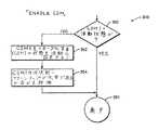
バックグラウンドクリーンアップは、CSMイネーブルアルゴリズム340が呼び出されたときに始まる。CSMイネーブル340は、固体メモリディスク60にホストが書込むたびに呼び出される。たとえば、CSMイネーブル340は図10、11の書込みアルゴリズムステップ260で呼び出される。CSMイネーブル340はCSM次状態ポインタをクリーンアップ状態に設定することによりクリーンアップ状態機械を起動する。
【0136】
その第1のクリーンアップ状態の実行は、トップレベルスケジューラ150がクリーンアップにCPU92の時間を割当てるたびに起こる。トップレベルスケジューラ150は1状態実行アルゴリズム346を呼び出すことによりこれを実行する。1状態実行346はCSM次状態ポインタにより指示される状態を呼び出す。その状態は、どちらの状態であれ、CPU92の状態を引き渡すのに先立って、次状態ポインタを変更する。従って、トップレベルスケジューラ150がクリーンアップに実行時間を割当てるたびに、1状態実行を呼び出すことにより別のステップが実行されるのである。
【0137】
フォアグラウンドクリーンアップはクリーンアップ164のサービス348を呼び出すことによって始まる。条件調整までマルチCSM実行348は、書込み要求に対して空きメモリを割当てることができないときに呼び出される。これは、それ以上の書込みを実行する前に空きメモリを生成する必要があるという決定を表わしている。条件調整までマルチCSM実行348は、2つのクリーンアップ状態機械をイネーブルすることによりこれを実行する。
フォアグラウンドクリーンアップ及びバックグラウンドクリーンアップとは対照的に、クリーンアップ強制342とマルチクリーンアップ強制344の双方はCPU52により呼び出される。クリーンアップ強制342は一方のクリーンアップ状態機械をイネーブルし、また、マルチクリーンアップ強制344は2つのクリーンアップ状態機械をイネーブルする。
【0138】
A.バックグラウンドクリーンアップ
1.バックグラウンドクリーンアップの開始とクリーンアップ状態の連係
バックグラウンドクリーンアップはCSMイネーブル340に対する呼び出しによって開始される。CSMイネーブル340の流れ図を図17に示す。
ステップ360におけるマイクロプロセッサ92の第1のタスクは、クリーンアップ状態機械1が既に活動状態であるか否かを判定することである。活動状態であれば、実行すべきことは何もない。その場合には、マイクロプロセッサ92は何もせずにステップ361へ分岐する。クリーンアップ状態機械1が活動状態でない場合、マイクロプロセッサ92はステップ362へ分岐する。
【0139】
ステップ362では、マイクロプロセッサ92はバックグラウンドクリーンアップを開始するために必要な2つの小さなタスクのうち第1のタスクを実行する。そこで、マイクロプロセッサ92は変数CSM1.statusを活動に設定することによりクリーンアップ状態機械1(CSM1)を活動状態にする。これを実行したならば、マイクロプロセッサ92はステップ364へ進む。
次に、マイクロプロセッサ92はバックグラウンドクリーンアップをセットアップするために要求される第2のタスクを実行する。これは、CSM1の次状態ポインタをクリーンアップが必要か否か評価状態380に設定することにより実行される。次に、トップレベルスケジューラ150が1状態実行346を呼び出したときに、バックグラウンドクリーンアップは始まる。そのジョブを実行したならば、マイクロプロセッサ92はステップ361へ分岐する。
【0140】
図18は、クリーンアップ状態機械の状態を互いに連鎖するアルゴリズムである1状態実行346の流れ図である。単一のアルゴリズムによって多数の状態を連鎖させるメカニズムは、CSM次状態ポインタである。各々のクリーンアップ状態機械は独自の次状態ポインタを有しており、そのポインタはそれぞれの状態の終了時に更新される。
1状態実行346に入ると、マイクロプロセッサ92は、CSM2.statusを検査することにより、第2のクリーンアップ状態機械CSM2が活動状態であるか否かを判定する。CSM2が活動状態でない場合、マイクロプロセッサ92はステップ370へ直接に分岐する。これに対し、フォアグラウンドクリーンアップがちょうど終了しようとしているときには、その結果、CSM2は活動状態になるであろう。この場合、マイクロプロセッサ92はステップ368でCSM2の別の状態を実行する。次に、ステップ374で制御を呼び出し側に戻す。
【0141】
CSM2がアイドル状態になると、CSM1が活動状態であれば、マイクロプロセッサ92はCSM1に注意を集中する。マイクロプロセッサ92はステップ370でこの決定を実行する。CSM1が非活動状態であれば、実行すべきことは何もないが、ステップ374で制御を呼び出し側に戻す。そうでない場合には、CSM1の次状態ポインタが指示している状態を実行する。その後、ステップ374で制御を呼び出し側に戻す。
【0142】
2.クリーンアップ状態機械の状態の概要
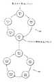
クリーンアップ中の事象の連鎖はどのようなものであろうか?簡単にいえば、クリーンアップはその種類にかかわらず3つの主要タスクを含む。第1に、クリーンアップの焦点として1つのブロックを選択する。第2に、良セクタごとに、ユーザーデータを焦点ブロックから宛先ブロックへ置き換える。ユーザーデータの置き換え自体は複数のステップから成るプロセスであって、メモリの割当てと、宛先ブロックへのセクタのコピーと、FLASHデータベース93の更新とを要求する。第3に、全てのユーザーデータを焦点ブロックからコピーし終わった後に、焦点ブロックを消去し、ダーティセクタを空きメモリに変換する。
【0143】
図19は、クリーンアップ状態機械の各々の状態を示すことにより、クリーンアップの概要を表わしている。図19の中の丸印はクリーンアップ状態機械の1つの状態、すなわち、1つのアルゴリズムを表わす。状態間の矢印は、1つの状態の終了時にCSM次状態ポインタにより指示される次状態を表わす。
バックグラウンドクリーンアップは、状態380で、クリーンアップが必要であるか否かを評価することによって始まる。フォアグラウンドクリーンアップと、強制クリーンアップの間には、クリーンアップが必要であるか否かの評価を飛び越す。クリーンアップが必要でなければ、マイクロプロセッサ92は状態396へ分岐する。これはマイクロプロセッサ92の制御をトップレベルスケジューラ150に戻す。これに対し、クリーンアップが必要であると考えられる場合には、いくつかのブロックをクリーンアップする。カウンタにより、選択された数のブロックを指示する。その後、CSM次状態ポインタによりマイクロプロセッサ92は次状態382へ指示される。
クリーンアップは、状態382で、クリーンアップのために焦点ブロックを選択することによって本格的に始まる。次に、次状態ポインタはマイクロプロセッサ92を状態383へと指示する。
【0144】
焦点ブロック中のダーティセクタをクリーンアップするのに先立って、ユーザーデータの有効セクタを安全に再配置しなければならない。このタスクは、焦点ブロック中のユーザーデータのあらゆるセクタが新たな記憶場所へ安全にコピーされ終わるまで、状態383、384、385、386及び388を通って繰り返し分岐することを要求する。ユーザーデータの再配置は、状態384で、ユーザーデータの1つの良セクタに対して新たな物理記憶場所を位置指定することによって始まる。新たな記憶場所として選択されるブロックを宛先ブロックという。この用語に従えば、クリーンアップは1つの焦点ブロックを有するが、宛先ブロックは数多くある。次に、CSM次状態ポインタはマイクロプロセッサ92に状態385を指示する。
【0145】
状態385では、焦点ブロックからセクタバッファ98へセクタをコピーする。
状態386では、マイクロプロセッサ92は有効セクタの一部をセクタバッファから現在宛先ブロックにコピーする。バックグラウンドクリーンアップがCPU52からの読取り指令及び書込み指令への応答に影響を及ぼすのを阻止するという希望に従って、書込み速度が与えられたならば、一度に有効セクタの一部のみをコピーすることになる。従って、1つの有効セクタが宛先ブロックに完全にコピーされる前に、マイクロプロセッサ92は何度か状態386を通過することになるかもしれない。有効セクタが完全にコピーされ終わったならば、CSM次状態ポインタはマイクロプロセッサ92を状態388に指示する。
【0146】
状態388の間、セクタ番号に関わるデータの以前のバージョンがダーティとマークされていなかった場合にセクタ見出し変換テーブル94が焦点ブロックからコピーしたばかりのセクタの新たな記憶場所を指示するように、マイクロプロセッサ92はセクタ見出し変換テーブル94を更新する。マークされていたならば、マイクロプロセッサ92はコピーしたばかりのセクタのバージョンをダーティとマークする。最終的には、マイクロプロセッサ92はそのセクタ番号に関わるセクタデータの新たなバージョンと関連する見出しの書込みを終了する。その後、マイクロプロセッサ92は状態384に戻る。
【0147】
状態383に再び入ると、マイクロプロセッサ92は焦点ブロック中のあらゆる良セクタを再配置し終わったか否かを判定する。再配置していなければ、再配置のために別の良セクタを選択し、焦点ブロック中の全ての良セクタを再配置し終わるまで、マイクロプロセッサ92は状態384、385、386、388及び383を通って分岐する。それが起こったとき、CSM次状態ポインタはマイクロプロセッサ92を状態390に指示する。
【0148】
マイクロプロセッサ92は、状態390で、焦点ブロックの消去を開始する。マイクロプロセッサ92は、チップ対に消去指令を発し且つ消去すべきブロックを指示することにより、消去を開始する。これを実行したならば、マイクロプロセッサ92は状態392へ進んで、消去が完了するのを待つ。焦点ブロックを含むチップ対が消去の完了を指示するまで、CSMは状態392にとどまる。
【0149】
焦点ブロックを消去したならば、マイクロプロセッサ92はブロック属性データ90を更新して、焦点ブロックに戻し、コピーする。これを実行した後、CSM次状態ポインタによりマイクロプロセッサ92に再び状態380を指示する。
状態380に再び入ると、マイクロプロセッサ92は、別の焦点ブロックを選択すべきか否かを判定するためにブロックカウンタを検査する。選択すべきであれば、先に説明した通りマイクロプロセッサ92は状態382、386、388、390、392及び394を通って分岐する。そうでない場合には、マイクロプロセッサ92はステップ396へ分岐して、クリーンアップを完了する。
【0150】
3.クリーンアップが必要であるか否かの評価
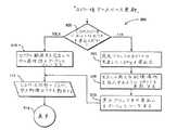
図20は、FLASHアレイ62をクリーンアップすべきか否かを評価するために状態380で使用するアルゴリズムを流れ図の形で示す。このアルゴリズムを使用した場合、総ダーティメモリが総メモリ予約の設定されたパーセンテージを越えたときに、バックグラウンドクリーンアップをトリガすることになる。総メモリ予約は総空きメモリ(TFFA)と、総ダーティメモリ(TDFA)との和として定義されている。総予約に対する総ダーティメモリのパーセンテージは固体ディスク60の性能と電力効率を左右する。
【0151】
マイクロプロセッサ92は、ステップ400で、評価が必要であるか否かを判定することにより動作を開始する。これは、以後にクリーンアップすべきブロックの数を確定するためにカウンタを検査することによって実行される。零より大きい数は、いずれも、クリーンアップが既にトリガされており、それ以上の評価は不要であることを指示する。マイクロプロセッサ92が初めて状態380に入ったとき、カウンタは零より小さいので、マイクロプロセッサ92は必然的にステップ402へ分岐することになる。
ステップ402では、マイクロプロセッサ92はFLASHアレイ62の中のダーティメモリの総量を総メモリ予約のパーセンテージとして計算する。
【0152】
ステップ404では、ステップ402で計算したパーセンテージをクリーンアップトリガポイントと比較する。クリーンアップトリガポイントは総メモリ予約の何らかのパーセンテージに固定されていても良いが、あるいは、CPU52の要求に基づいて適応変化されても良い。クリーンアップトリガポイントを適応変化させるためのアルゴリズムについては、後に詳細に説明する。総ダーティメモリがトリガポイントで等しいか又はそれを越える場合にはマイクロプロセッサ92はステップ406へ分岐することによりバックグラウンドクリーンアップを起動する。これに対し、総ダーティメモリのパーセンテージがトリガポイントを越えない場合には、マイクロプロセッサ92はステップ409へ分岐する。クリーンアップは不要であるので、CSM1の状態をアイドルに設定する。状態410へ分岐することにより、クリーンアップを開始することなく制御をトップレベルスケジューラ150に戻す。
【0153】
ステップ406では、マイクロプロセッサ92はブロックカウンタをクリーンアップすべきブロックの最大数に設定する。一実施例では、その最大数は3に設定される。これを実行したならば、マイクロプロセッサ92はステップ408へ進む。
ステップ408では、マイクロプロセッサ92はCSM次状態ポインタをクリーンアッププロセスにおける次の状態である状態382へ進める。これを実行したならば、マイクロプロセッサ92はステップ410へ分岐することにより制御をトップレベルスケジューラ150に戻す。
【0154】
クリーンアップが必要であるか否かを評価するための後続する呼び出しの間に、状態380において、マイクロプロセッサ92はステップ400でブロックカウンタを検査することによって動作を開始する。ブロックカウンタが零を越えれば、クリーンアップの必要は評価されない。その代わりに、マイクロプロセッサ92はブロックカウンタを減分し、ステップ401へ分岐する。
ステップ401では、マイクロプロセッサ92はCSM次状態ポインタを状態382に指示し、クリーンアップすべきブロックを選択する。次に、マイクロプロセッサ92は戻りステップ410を経て状態380から出る。
【0155】
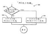
図21は、クリーンアップが必要であるか否かを評価するためにステップ404で使用されるトリガポイントを適応変化させるアルゴリズムを流れ図の形で示す。図示したアルゴリズムはセクタ162に属している。
ステップ412では、マイクロプロセッサ92はトリガポイントが余りに低く設定されていないかどうか、即ち、FLASHアレイ62がダーティになりすぎるようにされていないかどうかを判定する。Mを大きな数とするとき、マイクロプロセッサ92は、最前のM回の書込みの中で何回かのフォアグラウンドクリーンアップが起こったか否かを判定することによりこれを実行する。起こっていれば、マイクロプロセッサ92はステップ414へ進む。起こっていなければ、マイクロプロセッサ92はステップ416へ分岐する。
【0156】
ステップ414では、FLASHアレイ62がダーティになりすぎるようにされていたため、マイクロプロセッサ92はトリガポイントを少量だけ減少させる。これは、FLASHアレイ62が将来ダーティになるのを阻止するという効果をもつ。ステップ414から、マイクロプロセッサ92は制御を呼び出し側プログラムに戻す。
【0157】
ステップ416は、マイクロプロセッサ92は、FLASHアレイ62が余りにクリーンに保持されていないかどうかを考慮する。Nを大きな数とするとき、マイクロプロセッサ92は最前のN回の書込みの中のフォアグラウンド消去の回数を評価することによりこれを確定する。非常に長い時間にわたりフォアグラウンド消去が起こっていなければ、マイクロプロセッサ92はステップ418へ分岐する。起こっていたならば、マイクロプロセッサ92はトリガポイントを変更することなくステップ420へ進む。
【0158】
ステップ418では、マイクロプロセッサ92はトリガポイントをわずかに増加させる。これにより、バックグラウンドクリーンアップをトリガする前と比べてFLASHアレイ62はわずかにダーティになり、その結果、クリーンアップ効率は向上する。トリガポイントを調整したならば、ステップ420へ分岐することにより、マイクロプロセッサ92は呼び出し側プログラムに制御を戻す。
【0159】
4.クリーンアップすべきブロックの選択
クリーンアップをトリガしたならば、状態382では焦点ブロックを選択する。焦点ブロックを選択するときの目標は、最も費用有効性を高くクリーンできるブロックを選択することである。費用有効性のあるクリーンアップは、電力消費が過剰になるほどFLASHアレイ62をクリーンに保持することと、フォアグラウンドクリーンアップが頻繁に起こるほどFLASHアレイ62をダーティに保持することである。1つのブロックがクリーンアップに関して費用有効性のある焦点であるか否かを判定するときに、いくつかの係数を考慮すべきである。第1に、そのブロックがどれほどダーティであるかということである。ブロックがダーティになるほど、そのブロックを消去する費用有効性は高い。焦点を選択する場合、決定をフォアグラウンドクリーンアップを最小限に抑える方向に向かわせるために、この係数に最も大きな重みを付ける。第2に、焦点が一部を成しているチップ対にどれほどのメモリがあるかということである。この係数は、プログラムのために消去を延期する能力をもたないFLASHメモリデバイスについてのみ考慮される。消去を延期する能力をもたないFLASHデバイスの場合、単一のブロックの消去中、そのチップ対の中のどのブロックも利用不可能である。このため、同じチップ対の中に大量の空きメモリがある場合に1つの特定のブロックをクリーンアップする所望度は低下する。第3に、焦点ブロックの中にどれほどの有効ユーザーデータ、すなわち、良データが存在しているかということである。これにより、焦点からコピーしなければならないセクタの数は増加するので、焦点として特定の1ブロックを選択する所望度も低下する。逆に言えば、コピーしなければならない良セクタが少ないほど、ブロックをクリーンアップする所望度は高くなる。焦点ブロックを選択するときには、他の係数を考慮しても良い。
【0160】
図22は、先に論じた係数を使用して状態382でクリーンアップすべきブロックを選択するためのアルゴリズムを示す。簡単に説明すれば、FLASHアレイ62の中のブロックごとに1つのスコアを生成することにより、クリーンアップの焦点として1つのブロックを選択する。このスコアは、各々の係数を適切に重みづけし且つ重みづけした係数を加算することにより生成される。最も高い総スコアを有するブロックをクリーンアップの焦点として選択する。
【0161】
ステップ440では、全てのブロックを検査し終わったか否か、従って、焦点ブロックを選択したか否かを判定することにより、焦点ブロックの選択が始まる。マイクロプロセッサ92は、全てのチップ対を探索したか否かを判定することによりこれを実行する。ステップ440を始めて通過した後、検査されたチップ対は1つではないため、マイクロプロセッサ92はステップ442へ分岐する。
ステップ444では、マイクロプロセッサ92は選択したチップ対の中で検査すべき1つのブロックを選択する。あらゆるブロックを検査したわけではない場合には、次に、マイクロプロセッサ92はステップ448へ進む。
【0162】
ステップ445では、マイクロプロセッサ92は、ブロックが現在は別のクリーンアップ状態機械によるクリーンアップの焦点であるチップ対の一部であるか否かを判定する。これにより、クリーンアップの目標となっているチップの中の全てのブロックはいずれかの時点で長期間にわたり利用不可能となるので、現在ブロックは所望度の低い焦点ブロックになる。マイクロプロセッサ92は、RAMに記憶されているチップとブロックの情報を検査することにより、チップが別のクリーンアップ状態機械のクリーンアップの目標となっているか否かを判定することができる。この係数に重み1を乗算してRule 1を生成した後、マイクロプロセッサ92はステップ446へ進む。この第1のスコアは、現在ブロック中のダーティな語の総数TDFBC に第1の重みを乗算することにより生成される。この重みの値は後続する重みの値より相当に大きくなければならない。次に、マイクロプロセッサ92はステップ446からステップ448へ分岐する。
【0163】
マイクロプロセッサ92は、ステップ448で、現在ブロックに関わる第2のスコアを計算する。そこで、選択したチップ対の中の空きFLASHの総量TFFCC に第2の重みを乗算する。その後、マイクロプロセッサ92はステップ449へ分岐する。
第3のスコアはステップ449で計算される。そこで、現在ブロックが最前に消去されたチップ対の中にあるか否かによって、ブロックの所望度を評価する。その後、マイクロプロセッサ92はステップ450へ分岐する。
【0164】
ステップ450では、マイクロプロセッサ92は現在ブロックに関わる第4のスコアを計算する。マイクロプロセッサ92は、現在ブロック中の良バイトの総数をそのブロックの中のバイトの総数から減算することにより、このスコアを計算し始める。次に、マイクロプロセッサ92はこの数に第4の重みを乗算する。第4の重みは、焦点ブロックの選択を良さという点では劣るセクタデータを有するブロックを選択することにわずかに偏向させようとするものである。次に、マイクロプロセッサ92はステップ451へ分岐する。第4の重みは第1の重みと比較して相対的に小さい。
【0165】
現在ブロックに関わる第5の、そして、最後のスコアはステップ451の間に生成される。考慮される第5の係数は選択をサイクルカウントの低いブロック向かわせ、それにより、受動摩耗均等化を行うのである。アレイ62中の最大サイクルカウントと比較して現在ブロックのサイクルカウントが少ないほど、ブロックの所望度は高くなる。そこで、「Δサイクルカウント」により表わされるこの係数に第5の重みを乗算する。
【0166】
ステップ452では、マイクロプロセッサ92は現在ブロックの所望の特性を反映するRule 1、Rule 4及びRule 5を加算することにより、ブロックに関わる総スコアを生成する。Rule 0、Rule 2及びRule 3は焦点ブロックの望ましくない特性を指示しているので、この和からそれらを減算する。
ステップ454へ進むと、マイクロプロセッサ92は現在ブロックに関わる総スコアを最大総スコアと比較する。現在ブロックに関わる総スコアが最大総スコアを越えていれば、最大総スコアを上向きに改訂し、マイクロプロセッサ92はステップ456へ進む。これに対し、現在ブロックに関わる総スコアが最大総スコア以下である場合には、マイクロプロセッサ92はステップ444に戻る。
【0167】
ステップ456では、マイクロプロセッサ92は現在最大総スコアを有するブロックのチップ、ブロック及びスコアを記憶する。次に、マイクロプロセッサ92はステップ444に戻る。
ステップ444に再び入ると、マイクロプロセッサは現在選択したチップ対の中のあらゆるブロックを評価したか否かを決定する。全てのブロックを評価し終わっていなければ、選択したチップ対の中の全ブロックを評価し終わるまで、マイクロプロセッサ92はステップ446、448、450、452、454、456及び444を経て分岐する。選択したチップ対の中のブロックが評価されるたびに、マイクロプロセッサ92はステップ440に戻る。
ステップ440は、どのチップ対の中のブロックも検査されたか否かを判定する。検査されていなければ、FLASHアレイ62の中の全てのチップ対の全てのブロックを評価し終わるまで、マイクロプロセッサ92はステップ442、444、446、450、452、454、456及び440を経て分岐する。次に、マイクロプロセッサ92はステップ458へ進む。
【0168】
マイクロプロセッサ92はクリーンアップの焦点として選択したチップとブロックを焦点ウィンドウに書込む。マイクロプロセッサ92はステップ456で記憶したブロックとチップのアドレスを使用して、これを実行する。その後、マイクロプロセッサはステップ460へ進む。
現在の目標に到達したならば、ステップ460で、マイクロプロセッサ92は空き物理セクタを割当てるためにCSM次状態ポインタを設定する(状態384)。
ステップ460から、マイクロプロセッサ92はステップ462へ分岐することにより制御をトップレベルスケジューラ150に戻る。
【0169】
5.クリーンアップのための空き物理セクタの割当て
焦点ブロックを消去するのに先立って、焦点ブロックからユーザーデータの全ての有効セクタをコピーし、宛先ブロックへ再配置しなければならない。再配置プロセスにおける第1のステップは、焦点ブロックに現在入っているユーザーデータのセクタに対してメモリスペースを割当てることである。図23は、クリーンアップ中、メモリの割込みを管理する状態384に関わるアルゴリズムを示す。
【0170】
マイクロプロセッサ92は、ステップ472で、焦点ブロック中のあらゆる良セクタを再配置したか否かを判定することにより割当てを開始する。マイクロプロセッサ92は、次の見出しに到達するまで焦点ブロックのBSTT84を走査してゆくことによってその決定を実行する。見出しの中の属性語がFFFF(16進数)である場合、ユーザーデータのどのセクタも焦点ブロックからコピーされ終わっている。その場合、マイクロプロセッサ92は状態480へ分岐する。全ての有効セクタがコピーされたわけではない場合には、マイクロプロセッサ92はそのセクタが有効であるか又はダーティであるかを知るために属性語を検査する。ダーティセクタはマイクロプロセッサ92にBSTT84を次の見出しまで走査させる。マイクロプロセッサ92は、セクタのサイズを確定し且つステップ474へ進むことにより、良セクタに応答する。
【0171】
ステップ474では、マイクロプロセッサ92は、図10、11の割当てアルゴリズム又は後に説明する別のアルゴリズムを呼び出すことにより、ステップ472で識別したセクタに対してメモリを割当てる。
マイクロプロセッサ92は、ステップ476で、CSM次状態ポインタを状態385にリセットすることにより、状態384から出るべく準備する。すなわち、バックグラウンドクリーンアップが実行を再開するとき、焦点ブロックからセクタバッファ98へのセクタのコピーが始まる。これを実行したならば、マイクロプロセッサ92はステップ478へ分岐することにより制御をトップレベルスケジューラ150に戻す。
【0172】
焦点ブロックからあらゆる有効セクタがコピーされ終わるまで、マイクロプロセッサ92は何度も状態476に戻る。全セクタをコピーしたならば、マイクロプロセッサ92はステップ472からステップ480へ分岐する。ステップ480では、マイクロプロセッサ92は、消去を開始するためにCSM次状態ポインタを適切に設定することにより、焦点ブロックの消去を開始する。制御を呼び出しプログラムに戻す。
【0173】
6.クリーンアップのための空き物理メモリの割当て
図24は、クリーンアップのために空き物理メモリを割当てる別の方法を流れ図の形で示す。クリーンアップの宛先ブロックとして選択されるブロックは適切であると共に、所望のブロックでもなければならない。ブロックの適否をアクセスするときは、図10、11及び図13、14に示した割当て方法に関して先に論じたのと本質的に同じ方式を使用する。ただし、所望の宛先ブロックの評価と定義は異なる。最も所望度の高い宛先ブロックは、焦点ブロックからコピーすべきユーザーデータのセクタに最も厳密に適合するブロックである。このように宛先ブロックの所望度を定義すると、ホスト書込みのために大量の空きデータを保存することにより、ユーザーデータのコヒーレンシーは増大する。
【0174】
クリーンアップ中のメモリの割当ては、宛先ブロックの選択に際して使用する変数の初期設定をもって始まる。ステップ2202及び2204では、BestFit BlockとBest Fit Chipを共に0に設定する。
ステップ2206では、マイクロプロセッサ92は焦点ブロックの中に残っているユーザーデータのセクタを記憶するために必要な空きメモリの量を計算する。従って、一度に1つのセクタに関するメモリのみを割当てるのではあるが、焦点ブロックの中に残っているユーザーデータの全てのセクタを記憶できるブロックに関して所望度を評価することになる(ここでいう「ユーザーデータのセクタ」及び「ユーザーデータ」は空きでもなく、ダーティでもないメモリとして定義されている。)
【0175】
ステップ2207では、マイクロプロセッサ92は、考えうる宛先ブロックの評価を開始するのに先立って、もう1つの変数を初期設定する。Scoreをいずれかのブロックにおける空きメモリの最大量を表わす最大値に設定する。評価中、所望度が最も高い宛先ブロック、すなわち、利用可能な空きメモリが必要な総空きメモリに最も近いブロックのスコアを指示するために、Scoreを改訂する。これを実行したならば、マイクロプロセッサ92はステップ2208へ進む。
各ブロックの宛先ブロックとしての適否は図13、14に関して論じたのと同じ方式でステップ2208〜2216において評価される。従って、それらのステップについては詳細には説明しない。
【0176】
最終的には適切なブロックを識別し、マイクロプロセッサ92はステップ2218に至る。そこで、現在ブロックの宛先ブロックとしての所望度を確定する。宛先ブロックとしての所望度を図24のサービスに従って規定する係数が1つある。それは、現在の空きメモリの量が焦点ブロック中に残っているユーザーデータの全てのセクタを記憶するために必要とされる空きメモリの量とどれほど密接に一致するかということである。変数Totalは、焦点ブロックの中のユーザーデータを記憶した後に残っている空きメモリに関して現在ブロックの所望度を測定する。現在ブロック中の空きメモリが多すぎるか又は少なすぎるかに従って、Totalは正の数又は負の数になるであろう。次に、マイクロプロセッサ92はステップ2220へ分岐する。
【0177】
ステップ2220では、マイクロプロセッサ92は現在ブロックが最も良く適合するとして現在選択されているブロックよりも良く適合するか否かを判定する。言いかえれば、TotalCurrent Block の絶対値をScoreの絶対値と比較する。比較に際して絶対値を使用することにより、厳密に必要であるより空きメモリの少なすぎるブロックと、厳密に必要であるより多くの空きメモリを有するブロックの双方が確実に考慮されるのである。TotalCurrent Block の絶対値がScoreの絶対値より小さくない場合、マイクロプロセッサ92はステップ2208に戻って、別のブロックを評価する。これに対して、現在ブロックが以前のブロックより良く適合しているならば、マイクロプロセッサ92はステップ2222へ分岐して、最良適合値を改訂する。
【0178】
ステップ2222では、ScoreをTotalCurrent Block にリセットする。その後ステップ2224及び2226において、Best Fit ChipとBest Fit Blockをそれらが現在ブロックを指示するように改訂する。これを実行したならば、マイクロプロセッサ92はステップ2208に戻って、別のブロックを評価する。
FLASHアレイ62中の各ブロックを評価した後、マイクロプロセッサ92はステップ2208からステップ2228へ出る。次に、マイクロプロセッサ92は、Best Fit Blockに焦点ブロックから現在移動中であるデータのセクタを記憶するのに十分なメモリがあるか否かを判定する。十分なメモリがなければ、ステップ2230で、マイクロプロセッサ92は現在のクリーンアップ状態機械をアイドル状態とする。十分なメモリがある場合には、マイクロプロセッサ92はステップ2232へ進み、Best Fit Blockのメモリを実際に予約するプロセスを開始するのであるが、これは図10、11及び図13、14に関して先に説明したのと同じ方式で実行される。
【0179】
7.良セクタのコピー
焦点ブロックから宛先ブロックへのセクタのコピーは2つのステップから成るプロセスである。まず、焦点ブロックからセクタバッファ98へ有効なユーザーデータの選択されたセクタをコピーする。第2に、セクタバッファ98から宛先ブロックへ有効セクタをコピーする。この2ステッププロセスは不要なのであるが、シーケンサ168の経路中にある誤り検出回路の誤り検出能力を利用することによって、ユーザーデータの信頼性を改善する。
図25のアルゴリズムは、焦点ブロックからセクタバッファ98へのユーザーデータの1セクタのコピーを処理する。まず、ステップ480では、セクタをセクタバッファ98へ移動する。第2に、マイクロプロセッサ92はセクタの一部をコピーするように次状態ポインタを設定する。次に、ステップ484で、制御を呼び出し側に戻す。
【0180】
セクタバッファ98の一時保護から宛先ブロックへのセクタのコピーは、Copy Part of Sectorと呼ばれる状態386で実行される。状態386の実行時間が選択された最大実行時間より短くなるように保証するために、状態386が実行されるたびに、セクタの一部のみをコピーする。一実施例では、各々の状態の最大実行時間は500μ秒に限定されている。
【0181】
図26は、セクタバッファ98から1つのセクタの一部をコピーするためのアルゴリズムを示す。マイクロプロセッサ92は、ステップ490で、セクタの残り部分を最大実行時間の中で宛先ブロックにコピーできるか否かを決定することにより動作を開始する。一実施例では、セクタバッファ98から以後にコピーすべきバイトの数を20と比較することにより、マイクロプロセッサ92はこれを実行する。コピーできる語の最大数は、選択された最大実行時間によって異なる。セクタの残り部分を最大実行時間の中でコピーできないのであれば、マイクロプロセッサ92はステップ492へ分岐する。
ステップ492では、マイクロプロセッサ92はセクタバッファ98からクリーンアップ状態機械の宛先ウィンドウにより指示される宛先ブロックへ20バイトをコピーする。その後、マイクロプロセッサ92はステップ494へ分岐する。
【0182】
ステップ494では、マイクロプロセッサ92はCSM次状態ポインタを状態386に戻すように指示し、最終的にはセクタの全体がセクタバッファ98からコピーされるように保証する。マイクロプロセッサ92がステップ500へ分岐するとき、制御はトップレベルスケジューラ150に戻る。
最後に状態386を通過すると、残っている全ての語を最大実行時間の中で宛先ブロックへコピーすることができる。この通過の間に、マイクロプロセッサ92は状態490から状態496へ分岐する。
【0183】
ステップ496では、マイクロプロセッサ92はセクタバッファ98に残っている全ての語を宛先ブロックへコピーする。その後、マイクロプロセッサ92はステップ498へ進む。
有効セクタの宛先ブロックへの再配置を完了したならば、マイクロプロセッサ92はセクタの新たな物理記憶場所を反映するためにセクタ見出し変換テーブル94を更新すべく準備する。この時点で、マイクロプロセッサ92は新たなデータのセクタに関わる見出しの書込みをも終了する。これは、ステップ498で、CSM次状態ポインタを状態388にリセットすることにより実行される。セクタのコピーを終了したならば、マイクロプロセッサ92はステップ500を経て状態386から出る。
【0184】
8.セクタをコピーした後のデータベースの更新
ユーザーデータの1セクタが焦点ブロックから宛先ブロックへ完全に再配置されるまで、BSTT84とSHTT94の更新は遅延される。これにより、セクタが再配置中であっても、CPU52は常に確実にセクタの有効コピーをアクセスできるようになる。従って、セクタの移動中にCPU52は自在にそのセクタを再書込みできる。その結果FLASHアレイ62の中に同じデータのセクタの3つ以上のバージョンが存在しうるが、その中で、有効であるのは1つのバージョンのみである。これが起こったときには、マイクロプロセッサ92は状態386の間にダーティセクタを有効にコピーし終わっている。状態388のPostCopy Database Update(コピー後データベース更新)アルゴリズムは、どのデータベースを更新すべきか及びどのようにしてそれらのデータベースを更新すべきかを確定することにより、この問題を予想する。
【0185】
図27は、状態388の間のデータベースの更新を示す流れ図である。マイクロプロセッサ92は、ステップ502で、CSMがセクタをコピーしている間にホストがセクタを書込んだか否かを判定することにより、このタスクを開始する。マイクロプロセッサ92は、再配置したばかりのセクタに関わる見出しがダーティとマークされたか否かを検査することにより、これを判定することができる。この見出しを見出し(FOCUS)と呼ぶ。これがわかれば、マイクロプロセッサ92はどの変換テーブルを更新すべきか及びそれらのテーブルをどのように更新すべきをか知る。それには2つの可能性がある。
【0186】
まず初めに、見出し(FOCUS)がダーティとマークされないときの事象の列を考える。この状況においては、宛先ブロックと焦点ブロックの双方に関わるセクタ見出し変換テーブル94及びブロックセクタ変換テーブル84を更新しなければならない。これを実行し始めるために、マイクロプロセッサ92はステップ502からステップ506へ分岐する。
データベースの更新は宛先ブロックと共に始まる。ステップ506では、マイクロプロセッサ92はLSNは宛先ブロックのBSTT84に書込む。その後、マイクロプロセッサ92はステップ508へ分岐する。
マイクロプロセッサ92は、SHTT94の中のセクタのアドレスが焦点ブロックの見出しではなく、宛先ブロックの見出しを指示するように、そのアドレスを変更する。次に、マイクロプロセッサ92はステップ510へ進む。
【0187】
ステップ510では、マイクロプロセッサ92は3つの変換テーブル全ての更新を完了する。そこで、マイクロプロセッサ92は焦点ブロック中の見出しをダーティとマークする。マイクロプロセッサ92は、図15のダーティとマークするアルゴリズムを呼び出すことにより、これを実行する。データベースの更新を完了したならば、マイクロプロセッサ92はステップ512へ分岐する。
ステップ512に入ることは、1セクタのコピーが完了したことを指示している。マイクロプロセッサ92は、ステップ512で、空き物理セクタを割当てる状態384にCSM次状態ポインタを設定することにより、コピーすべき別の良セクタについて焦点ブロックを走査すべき準備する。
その後、ステップ514へ分岐することにより、マイクロプロセッサ92の制御はトップレベルスケジューラ150に戻る。
【0188】
セクタが宛先ブロックに再配置されている間にセクタが改訂されると何が起こるか?このセクタは既にダーティとマークされているので、見出し(FOCUS)を改訂する必要はない。また、SHTT94は既に改訂されたセクタと関連する見出しを指示しているので、SHTT94も改訂を要求しない。焦点ブロックの見出しが無効であることを表わすために、宛先ブロックのBSTT84のみを改訂すれば良い。マイクロプロセッサ92はステップ502からステップ516へ分岐することにより、このタスクを開始する。
マイクロプロセッサ92は、図15のダーティとマークするアルゴリズムを呼び出すことにより、ステップ516で宛先ブロックのBSTT84を更新する。先の場合と同様に、マイクロプロセッサ92はブロック514へ分岐することにより制御をトップレベルスケジューラ150に戻す。
【0189】
9.焦点ブロックの消去
消去を経たダーティセクタから空きメモリへの変換は、焦点ブロックから全ての良セクタをコピーした後に始まる。焦点ブロックの消去は消去を開始することと、次に、消去が終了するのを待つこととを含む。
図28は、状態390において消去を開始するためのアルゴリズムを示す。消去指令を発行するのに先立って、ステップ520では、マイクロプロセッサ92はブロック属性データ90をセクタバッファ98にコピーすることにより、ブロック属性データ90を保存する。
最後に、ステップ522では、マイクロプロセッサ92は焦点ブロックを含むチップ対へ消去指令を発行する。その時点では、待機することを除いて何も実行することは残っていない。
マイクロプロセッサ92は、ステップ524で、CSM次状態ポインタを消去完了を待機する状態392に設定することにより、長期間の待機を準備する。
【0190】
図29は、消去の完了を待機し且つ検出するために使用されるアルゴリズムを示す。ステップ530では、マイクロプロセッサ92は、チップ対の状態レジスタに問い合わせることにより消去が依然として進行中であるか否かを判定する。状態レジスタが消去は完了していないことを指示している限り、マイクロプロセッサ92はステップ532へ分岐する。そこで、マイクロプロセッサ92は、CSM次状態ポインタを消去完了を待機する状態392に設定することにより、その待機を継続すべく準備する。消去が完了したならば、マイクロプロセッサ92は状態534へ分岐し、そこで、CSM次状態ポインタを消去後更新状態394に設定する。
【0191】
10.消去後データベース更新
焦点ブロックを消去した後、いくつかのタスクが注意を要する。それらのタスクは、図30に示す消去後データベース更新状態394により管理される。
マイクロプロセッサ92が取り組む第1のタスクは、先の消去によって起こったサイクルカウントの数の増加を反映するために、FLASHアレイデータベースを更新することである。
マイクロプロセッサ92が実行する第2のタスクは、消去中にセクタバッファ98に記憶されていた新たなサイクルカウントをもつブロック属性データ90を焦点ブロックに復元することである。マイクロプロセッサ92はこれをステップ538で実行する。
【0192】
マイクロプロセッサ92はその最後の更新タスクをステップ540で実行する。そこで、ブロックがクリーンアップの焦点であることを指示するために、マイクロプロセッサ92はRAMに記憶されているセマフォーをクリアする。その結果、図12の割当てアルゴリズムは、可能であれば、先の焦点ブロックを含むチップ対に再び自在にセクタを割当てできる。
状態394から出る前に、マイクロプロセッサ92はCSM次状態ポインタを状態380、Evaluate IF Clean−Up is Necessaryにリセットする。
B.フォアグラウンドクリーンアップ
フォアグラウンドクリーンアップの目標は、FLASHアレイ62の中に大量の空きメモリを迅速に生成することである。フォアグラウンドクリーンアップは、2つのクリーンアップ状態機械を同時に動作させると共に、CPU52に空きメモリを強制的に待機させることにより、その目標を達成する。従って、フォアグラウンドクリーンアップはコンピュータのユーザーに影響を及ぼすことによりバックグラウンドクリーンアップとは異なる。フォアグラウンドクリーンアップは、バックグラウンドクリーンアップと比較してトリガされる方式についても異なっている。活動状態であるとき、バックグラウンドクリーンアップは、CPU52が1つのセクタを書込むたびに、それに続いて開始される。空き物理メモリの割当て中、フォアグラウンドクリーンアップはトリガされる。1つのセクタを書込むのに十分な空きFLASHメモリを割当てることができない場合、条件調整までマルチCSM実行348への呼び出しがフォアグラウンドクリーンアップを実行する。加えて、フォアグラウンドクリーンアップはクリーンアップが必要であるか否かの前述の評価によってバックグラウンドクリーンアップとは異なり、その決定は空きメモリの割当て中に有効に実行される。従って、フォアグラウンドクリーンアップは、クリーンアップすべきブロックを選択することにより開始する。
【0193】
図31は、フォアグラウンドクリーンアップを管理するために使用されるアルゴリズム、条件調整までマルチCSM実行348を示す。このアルゴリズムを使用すると、第1のクリーンアップ状態機械が起動され、消去完了待機状態392に到達するまで連続して動作することができる。その時点で、第2のクリーンアップ状態機械が動作され、消去完了待機状態392に到達するまで連続して動作することができる。そこで、第1のクリーンアップ状態機械は中断なく焦点ブロックのクリーンアップを完了する。1つのブロックがクリーンになり且つ別のブロックを間もなくクリーンにすべき場合、マイクロプロセッサ92はCPU52からの指令に再び応答する。
【0194】
フォアグラウンドクリーンアップはステップ550で始まり、そこでは、マイクロプロセッサ92は第1のクリーンアップ状態機械と、第2のクリーンアップ状態機械の双方について1のブロックカウントに設定する。先の図19の説明からわかる通り、ブロックカウントはどれほどの数のブロックをクリーンアップするか、従って、クリーンアップがどれほど長く続くかを確定する。双方のブロックカウントを1に設定することにより、フォアグラウンドクリーンアップの実行時間は最短に抑えられる。次に、マイクロプロセッサはステップ552へ進む。
【0195】
ステップ552と共に、マイクロプロセッサ92は双方のクリーンアップ状態機械を起動するプロセスを開始し、これはステップ562まで続く。マイクロプロセッサ92は、第1のクリーンアップ状態機械CSM1の状態を検査することにより、ステップ552で、CSM1が活動状態であるか否かを判定する。CSM1が活動状態でなければ、マイクロプロセッサ92は状態554へ分岐して、CSM1を起動する。これに対し、CSM1が既に活動状態である場合には、マイクロプロセッサ92はステップ558へ分岐して、第2のクリーンアップ状態機械CSM2を起動する。
ステップ554では、マイクロプロセッサ92はCSM1の状態をアイドルから活動へ変化させる。マイクロプロセッサ92はステップ554から556へ進む。
【0196】
マイクロプロセッサ92は、CSM1の次状態ポインタをクリーンアップすべきブロックを選択する状態382に設定することにより、CSM1にクリーンアップを開始させるべく準備する。これを実行したならば、マイクロプロセッサ92はステップ558へ分岐することにより、その注意をCSM2へ向ける。
ステップ558では、マイクロプロセッサ92はCSM2が活動状態であるか否かを判定する。活動状態であれば、マイクロプロセッサ92はステップ564へ進み、CSM1をランさせ始める。そうでない場合には、マイクロプロセッサ92はステップ560へ分岐する。
ステップ560では、マイクロプロセッサ92はCSM2を活動状態に設定する。その後、ステップ562で、マイクロプロセッサ92は、CSM2の次状態ポインタをクリーンアップすべきブロックを選択する状態382に設定することにより、CSM2にクリーンアップを開始させるべき準備する。
【0197】
2つのクリーンアップ状態機械のセットアップが完了したとき、マイクロプロセッサ92は最終的には一方を始動することができる。ステップ564では、マイクロプロセッサ94はどちらのクリーンアップ状態機械に実行時間を与えるべきかを判定する。マイクロプロセッサ92は、CSM1がブロックの消去を開始したか否かを判定することによりこれを実行する。CSM1が消去を開始していなければ、マイクロプロセッサ92はステップ566へ進む。
ステップ566では、マイクロプロセッサ92はCSM1の1つの状態を実行する。マイクロプロセッサは、消去完了待機状態392までのCSM1の状態を実行する。マイクロプロセッサ92はステップ566及び564を繰り返しループしてゆくことにより状態392に到達する。CSM1が消去完了待機状態392に到達すると、マイクロプロセッサ92は状態568へ分岐することにより、より効果の多い分野に注意を集中する。
【0198】
マイクロプロセッサ92は、ステップ568で、CSM2がその焦点ブロックのクリーンアップを終了するのにさらに実行時間を要求するか否かを判定する。要求するならば、マイクロプロセッサ92はステップ570へ分岐し、そこで、CSM2の単一の状態を実行する。マイクロプロセッサは、消去完了待機状態392までのCSM2の状態を実行する。この時点で、マイクロプロセッサはステップ570からステップ572へ分岐することにより、再びCSM1に注意を集中する。
ステップ572では、CSM1がその焦点ブロックのクリーンアップを完了したか否かを判定する。マイクロプロセッサ92は、CSM1と関連する状態語を検査することによりこれを実行する。CSM1がアイドル状態でない場合、マイクロプロセッサ92はステップ574へ分岐して、別のCSM1状態を実行する。ステップ572とステップ574の間を往復することにより、マイクロプロセッサ92はCSM1により管理されるクリーンアップを最終的に完了する。この時点で、1つのブロックは完全にクリーンアップされ終わっており、別のブロックが間もなくクリーンアップされることになる。既に大量の空きメモリの予約があるので、マイクロプロセッサ92はステップ576へ分岐することにより制御をトップレベルスケジューラ150に戻す。これにより、フォアグラウンドクリーンアップは終わる。
【0199】
C.強制クリーンアップ
強制クリーンアップは、クリーンアップ状態機械を起動し且つ制御するさらに別の方法である。強制クリーンアップは、コンピュータのユーザーからの指令により開始されるという点で、フォアグラウンドクリーンアップ及びバックグラウンドクリーンアップの双方とは異なっている。この種のクリーンアップでは、ユーザーは状態380におけるように空きメモリの総量を評価することなくクリーンアップが必要であると決定する。
固体ディスク制御装置64は2種類の強制クリーンアップを認識する。一方の型の強制クリーンアップは一方のクリーンアップ状態機械のみを起動する。この型のクリーンアップはForce Cleanup(強制クリーンアップ)と名付けられたサービス342により管理される。他方の型のクリーンアップは2つのクリーンアップ状態機械を起動し、ForceMulti Cleanup(強制マルチクリーンアップ)と呼ばれるサービス344により管理される。
【0200】
図32は、強制クリーンアップ342のアルゴリズムを示す。強制クリーンアップのタスクは相対的に単純である。すなわち、必要に応じて、CSM1を起動し且つ始動するのである。
ステップ580では、CSM1が活動状態であるか否かを知るためにCSM1の状態を検査することにより、マイクロプロセッサ92はそのタスクを開始する。活動状態であれば、マイクロプロセッサ92はステップ586へ分岐する。CSM1がアイドル状態である場合には、マイクロプロセッサ92はステップ587へ分岐する。
ステップ582では、マイクロプロセッサ92は、CSM1の状態を活動に変化させることによりCSM1をイネーブルする。次に、クリーンアップが必要であるか否かを評価する状態380をバイパスし且つCSM1の次状態ポインタをクリーンアップすべきブロックを選択する状態382に設定することにより、マイクロプロセッサ92は強制的にクリーンアップを開始させる。それが確実に実行されたならば、マイクロプロセッサ92はステップ584からステップ586へ分岐する。
【0201】
ステップ587では、CSM1が既にクリーンアップを開始していなかった場合に、マイクロプロセッサ92はCSM1に確実にクリーンアップを開始させる。マイクロプロセッサ92は、CSM1の次状態ポインタを検査し、それがクリーンアップは必要であると評価するのに等しい場合にはステップ584へ分岐することにより、これを実行する。これは、クリーンアップが不要であるという評価を全て回避する。
【0202】
図33は、強制マルチクリーンアップ344のアルゴリズムを示す。このアルゴリズムのタスクは、必要に応じて双方のクリーンアップ状態機械を起動することである。
強制マルチクリーンアップ344の初めと2つのステップは、強制クリーンアップ342のステップと全く同じである。ステップ590では、マイクロプロセッサ92はCSM1が活動状態であるか否かを判定する。活動状態でなければ、ステップ592でCSM1をイネーブルし、CSM1の次の状態としてコピーすべきブロックを選択する状態382を選択する。これに対し、CSM1が既に活動状態である場合には、マイクロプロセッサ92はステップ591へ分岐する。
【0203】
ステップ591では、マイクロプロセッサ92はCSM1がクリーンアップを開始したか否かを判定する。先に説明した通り、CSM1を起動するたびにブロックのクリーンアップが開始されるわけではない。次状態ポインタがクリーンアップは必要であるか否かを評価する状態以外の状態を指示する場合、クリーンアップは始まっている。この場合、マイクロプロセッサ92はステップ594へ直接に分岐する。そうでない場合、マイクロプロセッサ92はステップ592へ進む。
マイクロプロセッサ92は、そこで、CSM1の次状態ポインタをクリーンアップすべきブロックを選択する状態にリセットすることにより、CSM1に強制的に1つのブロックをクリーンアップさせる。その後、ステップ592からステップ594への分岐により注意はCSM2に向かう。
【0204】
ステップ594では、マイクロプロセッサ92は第2のクリーンアップ状態機械CSM2をイネーブルする。次に、マイクロプロセッサ92はクリーンアップが必要であるか否かを評価する状態380をバイパスし、CSM2の次状態ポインタをコピーすべきブロックを選択する状態382に設定する。マイクロプロセッサ92はステップ594からステップ596へ分岐して、制御をトップレベルスケジューラ150に戻す。
【0205】
IV.概 要
以上、固体メモリディスクを説明した。固体メモリディスクは、セクタごとにデータを記憶するFLASHメモリデバイスのアレイを含む。各々のメモリデバイスの中の各ブロックは、そのブロックに記憶されているセクタと、各セクタがブロック内のどこに位置しているかとを識別するブロックセクタ変換テーブルを維持している。固体ディスク制御装置はセクタデータのFLASHアレイからの読取り及びセクタデータのFLASHアレイへの書込みを管理する。制御装置は、1つのデータのセクタを書込むための指令を受信するたびに、セクタ番号を使用してそのセクタの以前のバージョンをシークする。与えられたセクタ番号と等しい論理セクタ番号を有するデータのセクタを見出すことによりセクタの以前のバージョンを位置指定したならば、それをダーティとマークする。その後、書込むべきデータのセクタに対して、異なる記憶場所にあるメモリスペースを割当てる。その結果、特定のセクタ番号と関連するセクタデータは1つの固定物理記憶場所にとどまるのではなく、FLASHアレイを巡って「浮動」する。
【0206】
以上の明細書の中では、本発明の特定の実施例を参照して本発明を説明した。しかしながら、特許請求の範囲に記載されるような本発明のより広範囲の趣旨から逸脱せずに本発明に対して様々な変形及び変更を実施しうることは明白であろう。従って、明細書及び図面は限定的な意味ではなく、例示としてみなされるべきである。
【図面の簡単な説明】
【図1】固体メモリディスクを含むパーソナルコンピュータのブロック線図。
【図2】固体メモリディスクのブロック線図。
【図3】ブロックファイル構造のブロック線図。
【図4】セクタ見出し変換テーブルの第1の実施例のブロック線図。
【図5】パワーアップ時にセクタ見出し変換テーブルを作成するためのアルゴリズムの流れ図。
【図6】固体ディスク制御装置のアルゴリズムのオブジェクト図。
【図7】ディスク読取りの流れ図。
【図8】ブロックセクタ変換テーブルを使用してデータの1セクタをシークするための流れ図。
【図9】1セクタを書込むための流れ図。
【図10】FLASHアレイ中でメモリスペースを割当てる第1の方法の流れ図。
【図11】FLASHアレイ中でメモリスペースを割当てる第1の方法の流れ図。
【図12】ブロックチェーンの図。
【図13】書込み指令に応答してメモリスペースを割当てる方法の流れ図。
【図14】書込み指令に応答してメモリスペースを割当てる方法の流れ図。
【図15】ダーティとマークするアルゴリズムの流れ図。
【図16】クリーンアップ中の様々なサービスのブロック線図。
【図17】クリーンアップ状態機械をイネーブルするための流れ図。
【図18】クリーンアップ状態機械の1つの状態を実行するための流れ図。
【図19】クリーンアップ状態機械の状態の流れ図。
【図20】クリーンアップをトリガすべきか否かを評価するためのアルゴリズムの流れ図。
【図21】クリーンアップを適応トリガするためのアルゴリズムの流れ図。
【図22】クリーンアップすべきブロックを選択するためのアルゴリズムの流れ図。
【図23】クリーンアップのためにメモリを割当てのための流れ図。
【図24】クリーンアップのための空き物理メモリを割当てる方法の流れ図。
【図25】セクタバッファに1セクタをコピーするための流れ図。
【図26】セクタバッファから宛先ブロックへ1セクタの一部をコピーするための流れ図。
【図27】1セクタをコピーした後にデータベースを更新するための流れ図。
【図28】ブロックの消去を開始するための流れ図。
【図29】ブロックの消去が完了したか否かを判定するための流れ図。
【図30】ブロック消去後にデータベースを更新するための流れ図。
【図31】フォアグラウンドクリーンアップに関わる流れ図。
【図32】強制クリーンアップに関わる流れ図。
【図33】クリーンアップを強制する別の方法の流れ図。
【符号の説明】
50 パーソナルコンピュータ
52 中央処理装置
54 モニタ
56 キーボード
58 マウス
60 固体ディスク
62 FLASHアレイ
64 固体ディスク制御装置
66 チップ対
68 上位チップ
70 下位チップ
80a、80b ブロック
84 BSTT
85 見出し
86 データスペース
90 ブロック属性データ
92 マイクロプロセッサ
93 データベース
94 SHTT
95 FLASHメモリ
96 ウィンドウASIC
98 セクタバッファ
100 電荷ポンプ
150 トップレベルスケジューラ
152 ホストインタフェース
154 FLASH媒体
156 ホストインタフェース
158 セクタバッファ
160 ディスク
162 セクタ
167 FLASHアレイインタフェース[0001]
[Industrial application fields]
The present invention relates to the field of computer storage systems. In particular, the present invention relates to solid state memory disks.
[0002]
[Prior art]
Many conventional personal computers include many types of memory storage devices. Hard magnetic disk drives are usually used for mass storage, and different types of semiconductor memory are used for other purposes.
[0003]
The non-volatility of hard magnetic disk drives is one of the main reasons they use. The hard drive can be turned on and off without losing data. A hard drive stores data in a plurality of concentric tracks. Each track contains several sectors, and each sector is typically 512 bytes long. Reading and writing to the magnetic disk drive occur one bit at a time.
A typical user file stored on a magnetic disk drive occupies a number of sectors randomly located on the surface of the disk drive. By storing a chain of pointers related to a file in a file allocation table (FAT), each sector of the file can be specified. Each pointer points to the next sector of the file.
[0004]
There are several drawbacks to hard drives. The size of a hard drive, especially its height, often makes the hard drive less interesting for use in portable computers and laptop computers. The height of the hard disk drive has often been one of the limiting factors in attempts to reduce the size of the computer to increase the portability of the computer. Also, hard drives consume a relatively large amount of power, making them more inappropriate for battery-powered computers.
Hard drives are not ideal for use in computers used outdoors. Magnetic disk drives are extremely susceptible to vibrations and shocks. In addition, magnetic drives do not fully tolerate the dust and moisture that is associated with much of the large outdoors.
[0005]
Many of the disadvantages of magnetic disk drives are not found in semiconductor memories, also called solid-state memories. Semiconductor memory is small and rugged and consumes significantly less power than a magnetic drive.
One type of non-volatile semiconductor memory is a FLASH electrically erasable programmable read only memory (FLASH memory). The FLASH memory is programmable by the user, and once programmed, it retains that data until it is erased. The FLASH memory is erased by erasing one block of memory at a time. One block is a relatively large amount of data of 64 Kbytes, that is, 65535 bytes.
[0006]
When the net charge on the floating gate is neutral, the FLASH memory cell is erased. The erased FLASH bit is referred to as “1”. Conversely, when the net charge on the floating gate is negative, the FLASH memory cell is programmed. The programmed FLASH bit is referred to as “0”. With one exception, it is impossible to reprogram a FLASH memory cell without first erasing it. Any FLASH bit can be programmed to 0 at any time.
[0007]
Some conventional FLASH memories internally control programming and erasing by means of a write state machine or command register. Internal programming and erasure control reduces the knowledge and time required to program and erase the FLASH memory. However, despite the internal control, the FLASH erase time remains relatively slow. The erase cycle time is about 1 to 2 seconds. If erasure must occur prior to each writing or rewriting of a sector of data, it is impossible to approximate the writing time of a magnetic disk drive using FLASH memory.
[0008]
[Problems to be solved by the invention]
One object of the present invention is to provide a solid state memory disk suitable for use in laptop computers and portable computers.
Another object of the present invention is to provide a solid state memory disk that is robust and relatively insensitive to shock and vibration.
Another object of the present invention is to provide a solid state memory disk that minimizes power consumption.
Another object of the present invention is to provide a solid state memory disk that allows outdoor dust and humidity.
Another object of the present invention is to provide a solid state memory disk that is lightweight.
It is yet another object of the present invention to provide a solid state memory disk that operates at least twice as fast as a hard disk drive.
[0009]
[Means for Solving the Problems]
A solid-state memory disk that stores data for each sector will be described. A solid state disk includes an array of FLASH memory semiconductor devices that store a plurality of sectors of data. Each block of memory in the FLASH array includes a data space for storing a number of sectors of data and a block sector conversion table. The block sector conversion table identifies each data sector stored in the data space of the block by a heading. The header includes a logical sector number equal to the sector number associated with the sector data. The solid state disk further includes a controller that controls the array. The controller has many responsibilities, among which the controller manages writing sector data to the array and reading sectors of data from the array. Each time the controller receives a command to write a sector of data associated with a given sector number, the controller seeks a previous version of that sector. If a previous version with a heading containing a logical sector number equal to the given sector number is located, mark it as dirty. Thereafter, memory spaces in different storage locations are allocated for sectors of data to be written. Finally, the sector of data is written into the allocated memory space. As a result, sector data associated with one sector number will not "float" around the FLASH array, rather than stay in one fixed storage location. The controller reads the sector of data by seeking the sector header conversion table to convert the sector number into a physical address.
[0010]
Other objects, features and advantages of the present invention will become apparent from the accompanying drawings and the following detailed description.
[0011]
【Example】
I.Overview of solid disks
FIG. 1 shows a personal computer 50 in the form of a block diagram. The personal computer 50 includes a central processing unit (CPU) 52 and a
[0012]
[0013]
Briefly described, the solid state disk of the present invention stores sector data by “floating” the sector data in the
[0014]
A.FLASH array and block file structure
Understanding the
[0015]
Erasing FLASH memory is a slow process. It is not practical to perform one erase every time one sector of data is written. Since the entire 128 Kbyte pair of blocks must be erased to write only one sector that is 512 bytes, the writing will be slow and the power consumption will be inefficient. In order to allow rapid sector writing, each time a sector is written, the solid
[0016]
Since FLASH memory is relatively expensive, the actual amount of FLASH memory within
[0017]
FIG. 2 shows the
[0018]
Each chip pair is organized as 16 blocks, each containing 128K bytes of memory. Since each block of memory can store multiple sectors of data, each block includes a block sector conversion table (BSTT) 84 for identifying and locating each sector of data.
[0019]
FIG. 3 shows a block 80 and the file structure used by that block and all other blocks. Although block 80 is represented as a one word wide structure, it is actually stored in two FLASH chips. The upper byte of each word is stored in the
The data structure of the block 80 includes a block sector conversion table 84 and a data space 86. Block sectorconversionThe table 84 stores a plurality of headings. The heading is a block composed of information on one logical sector number and its related data. The logical sector number (LSN) here refers to the sector number stored in the BSTT. The sector number is a sector identifier received from the
In one embodiment, each logical sector number is 24 bits long.
[0020]
Sector number while formatting diskEveryCreate one headline. Thereby, it is possible to detect the loss of the sector of data during the execution of the read command and the write command. Look at the heading associated with a specific sector number.OutWhen not, the sector of data associated with it is lostOopsI understand that. The term “loss” used herein refers to a sector of data that disappears due to a defect in the
[0021]
Each heading 85 includes a cyclic redundancy check (CRC) so that the
The heading 85 includes an attribute word that contains a large amount of information regarding the sector data associated with the heading. One bit in the attribute word indicates whether the sector number is marked as part of the bad track. Another bit indicates whether the sector data is compressed. The attribute word includes two dirty bits related to reliability. If both dirty bits are set, the sector data associated with the header is considered valid, and if either dirty bit is reset, it is considered dirty. The attribute word further includes data addition bits. If no sector data is added to the header, the data addition bit is reset. This is true for any heading after formatting. If data has been written for the sector number, the data append bit is set. The last information contained in the attribute word is the revision number. By this revision number, the solid-state
[0022]
The last information stored in the
[0023]
Memory space must be allocated to headings that do not have sector data attached. This is because during formatting, all of the BSTT 84 are filled with headings without data addition. Even if the entire data space 86 associated with those BSTTs 84 is free, writing to the data space 86 is impossible. This is simply because there is no room in the BSTT of those blocks. In order to avoid the catch 22 situation where free memory is not available for allocation, all of the data space 86 associated with those BSTTs 84 is classified as user data. In other words, the sector is neither dirty nor free as indicated by the dirty bit. Allocating a portion of the data space 86 as user data by allocating memory data space 86 to headings with no data attached and subtracting that amount of memory from the amount of free memory in the appropriate block, appropriate chip and array It is specified. While writing sectors of data after formatting, headers with no data attached are marked dirty along with their assigned data space. Eventually, the blocks filled during formatting are cleaned up and the data space becomes available as free memory.
[0024]
If data compression is not used, it is critical to be able to write headings without appending data. When data compression is not used, there are few reservations available for cleanup, and every possible sector of data will be written to
[0025]
In the data space 86, data related to one sector collides with data related to another sector.BecauseEach BSO indicates the most significant part of the data related to one sector and the least significant part of the data related to another sector. For example, BSO which is the block offset of
[0026]
The block sector conversion table 84 grows downward toward the data space 86. The first heading BSTT 84 is written in the uppermost part of block 80. The heading for each subsequent sector written in block 80 is stored below the previous heading.
[0027]
In contrast to BSTT 84, data space 86 grows upward. The first sector of data written to block 80 is written to the lowest portion of data space 86. The next sector of data to be written to the data space 86 is written immediately above the previous sector. For example, LSN2 Data related to LSN1 Located in a lower address range than the associated data.
[0028]
The number of sectors that can be stored in the data space 86 varies before entering the BSTT 84. This variability occurs because the sector size varies when the sector data is compressed. When accompanied by data compression, the size of the sector will vary from 256 words to just a few words. If the
[0029]
The
[0030]
The block 80 further stores block
[0031]
B.Solid disk controller hardware concept
Referring again to FIG. 2, reading, writing and cleanup of the
[0032]
C.FLASH array database and sector header conversion table
By storing information used repeatedly in a random access memory (RAM), the performance of the
1. The total number of dirty words in the FLASH array 62 (TDFA);
2. Total number of dirty words in each block (TDFBN);
3. The total number of free words (TFFA) in the
4). Number of empty words in each chip pair (TFFCM;
5. Total number of empty words in each block (TFFBN)
including.
[0033]
How the
A sector header conversion table (SHTT) 94 converts a sector number into a pointer to a sector of related data. It is preferable to store the
[0034]
To understand why
[0035]
There are several SHTT designs that solve this 19-bit dilemma. In one embodiment shown in FIG. 4, one pointer is stored for each of the 83300 sectors in which the number of data in an industry standard 40 MB disk drive may appear. Each entry of SHTT 94 stores only 16 bits. Four of those bits indicate the chip pair storing the sector data being sought. The other four bits indicate the specific block storing that sector. The remaining 8 bits represent the offset from the most significant portion of the block for the heading near the desired heading. This offset is called a heading pointer. Using 8 bits to represent a heading pointer means that 256 heading pointers can be used to locate up to 2047 headings. Thus, in order to locate the desired heading, a maximum of 8 headings must be scanned in BSTT 84. In other words, the SHTT 94a may require a two-step search to locate data associated with one specific sector number. First, the SHTT 94a is searched for specifying a specific chip, block, and header pointer. Second, the BSTT 84 indicated area is searched to find the headline associated with the sector number.
[0036]
The
[0037]
The
[0038]
Creation begins at
[0039]
In
[0040]
In
In
[0041]
[0042]
In
[0043]
On the other hand, if the sector is not dirty, the
[0044]
Entering
[0045]
In
[0046]
First, consider a simpler situation, that is, a case where data related to the sector number corresponding to the current LSN is not stored in the
[0047]
The situation is further complicated if
[0048]
In
[0049]
In
[0050]
Each time the heading within the
[0051]
II.Solid disk controller
The heart of the solid
[0052]
The object diagram of FIG. 6 shows the overall organization and interrelationship of the algorithms used by the solid
[0053]
Scheduling the host interface 152 and FLASH medium 154 is a relatively simple task. The power up of the
[0054]
Host interface 152 includes two classes of algorithms:
[0055]
Briefly, the FLASH medium 154 includes five services: five services:
[0056]
A.Read sector from FLASH array
Briefly, reading one sector is a three stage process. First, the
The read algorithm implemented by the
[0057]
The first task of
[0058]
If the calling program has given an invalid sector number, the
[0059]
On the other hand, if the caller requests to read a sector having a valid sector number, the
[0060]
In
[0061]
On the other hand, if there is a heading for the sector number, the
[0062]
If
[0063]
FIG. 8 shows a method of seeking sector data when a sector number is given. This algorithm is also realized by the
In brief, the seek algorithm of FIG. 8 has two schemes for locating data associated with sector numbers. The first scheme relies on data coherency to reduce seek time. That is, it is assumed that the sector of data currently being sought is related to and located in the vicinity of the sector of data that was previously positioned. If this scheme fails to locate the sector of the desired data, then a two-stage scheme is used. First, the sector number input SNi Search SHTT 94 to locate the chip, block and heading offsets associated with. The information is then used to search BSTT 84 for a heading with an LSN equal to the sector number entered by the caller.
[0064]
Data sector position designation begins at
[0065]
First, consider the action of the
[0066]
The process of determining the reliability of the current heading begins with
[0067]
First, consider the action of the
If this is successful, the method comprising steps 190-202 reduces the time required to locate a sector of data by a quarter compared to the two-step search comprising steps 206-222.
[0068]
The two-stage search begins at
[0069]
The second phase of seeking begins at
[0070]
The maximum number of headings that must be scanned is set by dividing the maximum number of headings in BSTT 84 by the maximum number of heading pointers. For example, in one embodiment of fixed
[0071]
First, consider the situation when the scan count is less than the maximum value.
In
[0072]
When the LSN is equal to the input sector number, the
Therefore, the
In
[0073]
If the current heading is not reliable, the
[0074]
If the current heading can be trusted, the
[0075]
B.Write sector to FLASH
Writing a sector of data includes three main tasks. First, enough free memory must be located and reserved to write the sector data. Second, if there is a previous version of sector data in the same LSN, it is marked as dirty and the sector header conversion table 94 is updated. Third, write the sector data and its header into the appropriate block.
[0076]
FIG. 9 shows a sector of one dataTheFLASH array 62InProvides an overview of the writing process. For writing, the
[0077]
First of all, SNi Consider the result when is invalid. The first action of the
[0078]
If SNi is invalid, the
This time, SNi Is valid and its attribute word is SNi Suppose that it indicates that the track associated with is marked as bad. SNi Is valid, the
[0079]
Preparation for writing a sector begins in earnest at
[0080]
In
In
[0081]
SNi The
As you can see from the previous explanation, SNi Is invalid or the associated track has been marked bad, the sector of data is not written to the
[0082]
In
[0083]
In
[0084]
[0085]
The
[0086]
If the new version of the sector data has been written reliably, in
[0087]
In
During step 262, the
[0088]
C.Allocating memory space when writing
Allocation of memory space within the
[0089]
The fourth decision is a difficult decision because whether a block is an appropriate block depends on several factors. First, the selected block cannot be included in the chip pair in use. Waiting on a pair of chips in use avoids this because it slows down the speed followed by the command from the
[0090]
10 and 11 are flowcharts of algorithms for allocating memory that can be used for host writes or cleanup. The illustrated algorithm belongs to
[0091]
Several results can occur when using the allocation algorithms of FIGS. First, consider the result that gives the greatest interest, ie, the case of allocating memory. Other results will be considered later.
Memory allocation begins by determining whether memory is requested for cleanup or for host writes. If cleanup requires free physical memory,
[0092]
At
[0093]
In
[0094]
[0095]
[0096]
[0097]
With this understanding of the blockchain, we return to the location of the block with sufficient memory according to the allocation algorithm of FIGS. In
[0098]
In
[0099]
In step 286, the
In step 2888, the
[0100]
In
Here, the
[0101]
In
[0102]
Assuming that the memory will be allocated previously, the
[0103]
[0104]
In
[0105]
If a block with enough room to store a sector is located, the
[0106]
In
By branching to step 300, the
[0107]
Finally, in
[0108]
There are several situations where memory space cannot be allocated using the algorithms of FIGS. Perhaps memory cannot be allocated because the
[0109]
In step 306, the
If the caller is the
[0110]
If memory cannot be allocated and the caller is one of the cleanup state machines, there is little to do. As described in detail below, foreground cleanup uses two or more cleanup state machines. In one embodiment, foreground cleanup uses two cleanup state machines. The first cleanup state machine operates without interruption until it begins to erase the block. At the start of erasure, the second cleanup state machine is started. However, it may not be possible to allocate memory for the second cleanup state machine because too many blocks are not available for erasure by the first cleanup state machine. When cleanup by the first cleanup state machine is complete, this is not a significant danger since a large amount of free memory has been formed. At
[0111]
FIGS. 13 and 14 illustrate, in flowchart form, another method of allocating free physical memory for host writes. Similar to the method of FIGS. 10 and 11, the selection of a block to which a write is to be assigned would include up to four decisions. Two of the decisions for allocating memory are performed in much the same manner as performed according to the method of FIGS. Those decisions are
1. Is there enough reserved memory to allow writing?
2. Is the block appropriate for allocating writes?
These are two. The method of FIGS. 13 and 14 does not select the first block with sufficient memory to store the sector of data to be written, as was done in the method of FIGS. Selecting a new block with a large amount of free memory for host write allocation increases data coherency for host writes. As a result of selecting the block with the most amount of free memory, more writes will be assigned to the selected block until there is insufficient free memory to store another sector of data. An amount of host data exists in the same block. This allocation method increases data coherency.
[0112]
In
[0113]
In order to increase data coherency and reduce the possibility of data fragmentation, at
[0114]
In
[0115]
[0116]
Block selection begins at
[0117]
Step1214Then, the
[0118]
In
[0119]
During
[0120]
In
[0121]
Exiting from
[0122]
The desirability of the current block is also evaluated by the amount of dirty memory TDFB in the current block. In
[0123]
Another factor evaluated in accessing the desired degree of the current block is the number cycle count of the current block compared to the maximum cycle count in the
The microprocessor accesses the fifth and last coefficient of the desired degree of the current block at
[0124]
In
[0125]
After all the blocks have been evaluated, the
[0126]
Entering step 1260 means that the
[0127]
Eventually, a block having enough space to store a sector of data is identified, and
[0128]
D.Marking a sector version as dirty
FIG. 15 shows, in flowchart form, an algorithm for the operation of marking a sector dirty, implemented by
[0129]
The algorithm for marking dirty requires three types of information: chip, block, and header offsets related to the sector data to be marked dirty. Given this information, the first task of
[0130]
Entering
[0131]
If the chip pair storing the previous copy of the sector data is not in use, the
[0132]
III.Solid disk cleanup
Each time a sector of data is revised, the solid
[0133]
Briefly, cleanup includes three main tasks. First, select a block as the focus of cleanup. Second, the sector of valid user data is copied from the focal block to another block called the destination block. Third, after all the valid sectors are copied from the focal block, the focal block is erased and the dirty sector is converted to free memory.
Cleanup is generally a background process. Since reads and writes to the
[0134]
Cleanup is managed by a finite state machine called a cleanup state machine. That is, cleanup is performed using a limited number of states that are chained together, ie, an algorithm. Each cleanup state indicates the next state, and each state is actually chained to another state. Each state does not require 500 μs or more as the execution time of the
Background cleanup uses a single cleanup state machine and is allowed execution time only when the host interface 152 is inactive. In contrast, during the foreground cleanup of the
[0135]
Both background cleanup and foreground cleanup are handled by the
Background cleanup begins when the CSM enable
[0136]
The execution of the first cleanup state occurs each time the
[0137]
Foreground cleanup begins by calling
In contrast to foreground and background cleanup, both
[0138]
A.Background cleanup
1.Linking the start of background cleanup and cleanup status
Background cleanup is initiated by a call to CSM enable 340. A flowchart of the CSM enable 340 is shown in FIG.
The first task of the
[0139]
In
[0140]
FIG. 18 is a flow diagram of a one-
Upon entering the one
[0141]
When CSM2 goes idle,
[0142]
2.Cleanup state machine status overview
What is the chain of events during cleanup? Simply put, cleanup involves three main tasks, regardless of type. First, select one block as the focus for cleanup. Second, the user data is replaced from the focal block to the destination block for each good sector. The user data replacement itself is a multi-step process that requires memory allocation, sector copying to the destination block, and
[0143]
FIG. 19 represents an overview of cleanup by showing the state of each of the cleanup state machines. The circles in FIG. 19 represent one state of the cleanup state machine, i.e. one algorithm. The arrow between states represents the next state indicated by the CSM next state pointer at the end of one state.
Background cleanup begins at
Cleanup begins in earnest at
[0144]
Prior to cleaning up dirty sectors in the focal block, valid sectors of user data must be safely relocated. This task requires repeated branching through
[0145]
In
In
[0146]
During
[0147]
State 383Once again, the
[0148]
[0149]
If the focal block is erased, the
Upon reentering
[0150]
3.Assessing whether cleanup is necessary
FIG. 20 illustrates in flowchart form the algorithm used in
[0151]
In step 402, the
[0152]
In
[0153]
In
In
[0154]
During subsequent calls to evaluate whether cleanup is necessary,
In
[0155]
FIG. 21 shows, in flowchart form, an algorithm for adaptively changing the trigger point used in
In
[0156]
At
[0157]
Step 416 causes the
[0158]
In
[0159]
4).Selecting blocks to clean up
If cleanup has been triggered,
[0160]
FIG. 22 shows an algorithm for selecting blocks to be cleaned up in
[0161]
In
In
[0162]
In
[0163]
A third score is calculated at
[0164]
In
[0165]
A fifth and final score for the current block is generated during
[0166]
In
Proceeding to step 454, the
[0167]
In
Upon reentering
Step 440 determines whether a block in any chip pair has been examined. If not,
[0168]
If the current goal has been reached, at
From
[0169]
5.Free physical sector allocation for cleanup
Prior to erasing the focal block, all valid sectors of user data must be copied from the focal block and relocated to the destination block. The first step in the relocation process is to allocate memory space for sectors of user data currently in the focus block. FIG. 23 shows the algorithm involved in
[0170]
[0171]
In
[0172]
The
[0173]
6).Allocating free physical memory for cleanup
FIG. 24 illustrates in flowchart form another way of allocating free physical memory for cleanup. The block chosen as the destination block for cleanup must be appropriate and must also be the desired block. When accessing block adequacy, we use essentially the same scheme discussed above with respect to the allocation methods shown in FIGS. However, the evaluation and definition of the desired destination block are different. The most desired destination block is the block that most closely matches the sector of user data to be copied from the focus block. Defining the desirability of the destination block in this way increases the coherency of user data by storing a large amount of free data for host writing.
[0174]
Memory allocation during cleanup begins with the initial setting of variables used in selecting the destination block. In
In
[0175]
In
The suitability of each block as a destination block is evaluated in steps 2208-2216 in the same manner as discussed with respect to FIGS. Therefore, those steps will not be described in detail.
[0176]
Eventually, the appropriate block is identified and
[0177]
[0178]
In
After evaluating each block in the
[0179]
7).Good sector copy
Copying sectors from the focus block to the destination block is a two step process. First, a selected sector of valid user data is copied from the focus block to the
The algorithm of FIG. 25 processes one sector of user data from the focus block to the
[0180]
The copying of the sector from the temporary protection of the
[0181]
FIG. 26 shows an algorithm for copying a part of one sector from the
In
[0182]
In
Finally, after passing through
[0183]
In step 496, the
Once the relocation of the valid sector to the destination block is complete, the
[0184]
8).Updating the database after copying sectors
The update of BSTT 84 and
[0185]
FIG. 27 is a flow diagram illustrating database updates during
[0186]
First, consider the sequence of events when the heading (FOCUS) is not marked dirty. In this situation, the sector header conversion table 94 and the block sector conversion table 84 relating to both the destination block and the focal block must be updated. To start doing this, the
The database update begins with the destination block. In
[0187]
In
Entering
Thereafter, by branching to step 514, the control of the
[0188]
What happens if a sector is revised while the sector is being relocated to the destination block? Since this sector is already marked dirty, there is no need to revise the heading (FOCUS). Also, since
[0189]
9.Clear focus block
The conversion from dirty sectors that have been erased to free memory begins after all good sectors have been copied from the focal block. Erasing the focal block includes starting the erase and then waiting for the erase to finish.
FIG. 28 shows an algorithm for initiating erasure in
Finally, in
In
[0190]
FIG. 29 shows the algorithm used to wait and detect the completion of erasure. In
[0191]
10.Update database after erasure
After erasing the focus block, some tasks require attention. These tasks are managed by the post-erase
The first task addressed by the
The second task performed by the
[0192]
Prior to exiting
B.Foreground cleanup
The goal of foreground cleanup is to quickly generate a large amount of free memory in the
[0193]
FIG. 31 shows the algorithm used to manage foreground cleanup,
[0194]
Foreground cleanup begins at step 550, where
[0195]
Along with
In
[0196]
In
In step 560, the
[0197]
When the setup of the two cleanup state machines is complete, the
In
[0198]
In
[0199]
C.Forced cleanup
Forced cleanup is yet another way to activate and control a cleanup state machine. Forced cleanup is different from both foreground cleanup and background cleanup in that it is initiated by a command from a computer user. With this type of cleanup, the user determines that cleanup is necessary without evaluating the total amount of free memory as in
The
[0200]
FIG. 32 shows the forced
In
In
[0201]
In
[0202]
FIG. 33 illustrates the forced
The beginning and two steps of the forced
[0203]
In
[0204]
In
[0205]
IV.Overview
The solid memory disk has been described above. A solid state memory disk includes an array of FLASH memory devices that store data by sector. Each block in each memory device maintains a block sector conversion table that identifies the sectors stored in that block and where each sector is located in the block. The solid state disk controller manages reading of sector data from the FLASH array and writing of sector data to the FLASH array. Each time the controller receives a command to write a sector of data, it uses the sector number to seek the previous version of that sector. If you located a previous version of a sector by finding a sector of data with a logical sector number equal to the given sector number, mark it dirty. Thereafter, memory spaces in different storage locations are allocated to sectors of data to be written. As a result, sector data associated with a particular sector number does not stay in one fixed physical storage location, but “floats” around the FLASH array.
[0206]
In the foregoing specification, the invention has been described with reference to specific embodiments of the invention. However, it will be apparent that various modifications and changes may be made thereto without departing from the broader scope of the invention as set forth in the claims. The specification and drawings are accordingly to be regarded in an illustrative rather than restrictive sense.
[Brief description of the drawings]
FIG. 1 is a block diagram of a personal computer including a solid-state memory disk.
FIG. 2 is a block diagram of a solid-state memory disk.
FIG. 3 is a block diagram of a block file structure.
FIG. 4 is a block diagram of a first embodiment of a sector header conversion table.
FIG. 5 is a flowchart of an algorithm for creating a sector header conversion table at power-up.
FIG. 6 is an object diagram of an algorithm of a solid disk control device.
FIG. 7 is a flowchart of disk reading.
FIG. 8 is a flowchart for seeking one sector of data using a block sector conversion table;
FIG. 9 is a flowchart for writing one sector.
FIG. 10 is a flow diagram of a first method for allocating memory space in a FLASH array.
FIG. 11 is a flow diagram of a first method for allocating memory space in a FLASH array.
FIG. 12 is a diagram of a block chain.
FIG. 13 is a flowchart of a method for allocating memory space in response to a write command.
FIG. 14 is a flowchart of a method for allocating memory space in response to a write command.
FIG. 15 is a flowchart of an algorithm for marking as dirty.
FIG. 16 is a block diagram of various services during cleanup.
FIG. 17 is a flow diagram for enabling a cleanup state machine.
FIG. 18 is a flow diagram for performing one state of a cleanup state machine.
FIG. 19 is a flow diagram of the state of the cleanup state machine.
FIG. 20 is a flowchart of an algorithm for evaluating whether cleanup should be triggered.
FIG. 21 is a flowchart of an algorithm for adaptively triggering cleanup.
FIG. 22 is a flowchart of an algorithm for selecting a block to be cleaned up.
FIG. 23 is a flow diagram for allocating memory for cleanup.
FIG. 24 is a flowchart of a method for allocating free physical memory for cleanup.
FIG. 25 is a flowchart for copying one sector to the sector buffer.
FIG. 26 is a flowchart for copying a part of one sector from a sector buffer to a destination block;
FIG. 27 is a flowchart for updating a database after copying one sector;
FIG. 28 is a flowchart for starting block erasure.
FIG. 29 is a flowchart for determining whether or not block erasure has been completed;
FIG. 30 is a flowchart for updating a database after block erasure.
FIG. 31 is a flowchart related to foreground cleanup.
FIG. 32 is a flowchart related to forced cleanup.
FIG. 33 is a flow diagram of another method for forcing cleanup.
[Explanation of symbols]
50 Personal computer
52 Central processing unit
54 Monitor
56 keyboard
58 mouse
60 solid disc
62 FLASH array
64 Solid disk controller
66 chip pairs
68 Upper chip
70 Lower chip
80a, 80b block
84 BSTT
85 headings
86 Dataspace
90 Block attribute data
92 Microprocessor
93 Database
94 SHTT
95 FLASH memory
96 window ASIC
98 sector buffer
100 charge pump
150 Top Level Scheduler
152 Host interface
154 FLASH media
156 Host interface
158 sector buffer
160 discs
162 sectors
167 FLASH array interface
Claims (4)
Translated fromJapanesea)入力セクタ番号を伴う、データのセクタの書込み要求を受信し、
b)このセクタ番号と同じ番号を持つ見出しがすでに存在しないか否かを調べ、
c)存在する場合は、その見出しをダーティとマークし、
d)データのセクタの書込み要求に応答して上記のセクタ番号を有するデータのセクタと見出しとを書込む第1の量の空きメモリを割当て、
e)上記ステップd)で用意された空きメモリの、データスペースにはデータのセクタを、ブロックセクタ変換テーブルにはデータのセクタに関連したセクタ番号に等しい論理セクタ番号とセクタオフセットをそれぞれ書込むことを特徴とするセクタデータを書込む方法。It has a plurality of memory blocks and can be erased only in units of blocks .Each block has a data space for storing a plurality of data sectors and a block sector conversion table . The block sector conversion table is a block. Amethod of writing sector data to a solid-state memory disk including a sector number for each sector stored in the sector and a sector offset indicating an offset to thesector data ,
a)receiving a write request for a sector of data with an input sector number ;
b)Check if there is already a heading with the same number as this sector number ,
c) if present, mark the header as dirty ,
d) allocating afirst amount of free memory to write the data sector and heading having the sector number in response to a data sector write request ;
e) Write the data sector in the data space of the free memory prepared in step d) above, and write thelogical sector number and sector offset equal to the sector number associated with the data sector in the block sector conversion table. A method of writing sector data characterized by
a)第1のデータのセクタを書込むための指令と、その第1のデータのセクタと関連する第1のセクタ番号とを受信し、
b)上記第1のセクタ番号と関連しているデータのセクタの以前のバージョンをダーティとマークし、
c)第1のブロックセクタ変換テーブルを有する第1のブロック内の第1の量の空きメモリを割当て、
d)第1のデータのセクタに関わる第1の見出しを第1のブロックセクタ変換テーブルに書込み、
e)第1のデータのセクタを第1のブロックに書込むことを特徴とする固体メモリディスクの制御方法。It contains a plurality of blocks and can be erased only in units of blocks . Each block stores a plurality of data sectors and a block sector conversion table. The block sector conversion table stores the data stored in the block. A solid-state memory disk containing one heading per sector, each heading including a logical sector number equal to the sector number with which the heading is associated, and a sector offset indicating an offset to the sector data associated with the heading. A control method ,
a) receiving a command for writing a sector of the first data and a first sector number associated with the sector of the first data;
b) marking the previous version of the sector of data associated with the first sector number as dirty;
c) allocates a first amount of free memory in the firstblock having a first block sector translation table,
d) Write the first heading relating to the sector of the first data to the first block sector conversion table;
e) Amethod for controlling a solid-state memory disk, wherein a sector of first data is written to a first block.
a)データのセクタを記憶するFLASHメモリデバイスのアレイと、
b)第1のデータのセクタと関連する第1のセクタ番号を使用して、セクタデータに関わる物理アドレスを生成するセクタヘッダ変換テーブルを具備し、書込み指令に応答してアレイに第1のデータのセクタを書込み且つ読取り指令に応答してアレイから第1のデータのセクタを読取り、アレイを制御する制御装置とからなり、
上記FLASHメモリデバイスのアレイは、FLASHアレイ内の各メモリブロックはブロック単位でのみ消去可能であり、各ブロックは複数のデータのセクタを記憶するデータスペースと、ブロックセクタ変換テーブルと有しており、ブロックセクタ変換テーブルはブロックのデータスペースに記憶されている各セクタのデータをセクタ番号によって識別し、
上記制御装置は、書込み指令に応答して上記セクタ番号と等しい論理セクタ番号を有するデータのセクタの以前のバージョンをダーティとマークし、データのセクタを記憶するデータスペースのために空きメモリを割当ててそこにデータのセクタを書き込み、セクタヘッダ変換テーブルをシークしてセクタ番号を物理アドレスに変換してデータのセクタを読み出すことを特徴とする固体メモリディスク。A solid-state memory disk storing a plurality of sectors of data each having a sector number,
a) an array of FLASH memory devices that store sectors of data;
b)using afirst sector numberassociated with the sectors of thefirstdata,comprising a sector header conversion table for generating the physical address related to the sector data, the first data into the array in response to a write command A controller for controlling the array by reading a sector of the first data from the array in response to a write and read command of the array;
In the FLASH memory device array, each memory block in the FLASH array can be erased only in units of blocks, and each block has a data space for storing a plurality of data sectors, and a block sector conversion table. The block sector conversion table identifies the data of each sector stored in the block data space by the sector number,
In response to the write command, the controller marks the previous version of the sector of data having a logical sector number equal to the sector number as dirty and allocates free memory for the data space storing the sector of data. A solid-state memory disk, wherein a sector of data is written therein, a sector header conversion table is sought, a sector number is converted into a physical address, and a sector of data is read out .
a)書込み指令に応答して第1のブロック内の第1の複数の記憶場所を割当てる割当て手段と、
b)セクタオフセットを第1のブロックのブロックセクタ変換テーブルに書込み、データのセクタを第1の複数の記憶場所に書込み、且つセクタ番号と等しい論理セクタ番号を第1のブロックのブロックセクタ変換テーブルに書込む書込み手段とを具備する制御装置。A plurality of blocks,can only be erased in blocks, each blockincludes a plurality of memory locationsand block sector translationtablefor storing sectors of data, the the block sector conversion table block and the sector number of each sector is stored, and a sector offset, sector offseta control device for controlling the solid-state memory disks to indicate the offset to the sector data,
a) allocating means for allocating the first plurality of storage locations in the first blockin response to the write command;
b) Write the sector offset to the block sector conversion table of the first block, write the sector of data to the first plurality of storage locations, and write the logical sector number equal to the sector number to the block sector conversion table of the first block A control device comprising writing means for writing.
Applications Claiming Priority (2)
| Application Number | Priority Date | Filing Date | Title |
|---|---|---|---|
| US07/969,131US5822781A (en) | 1992-10-30 | 1992-10-30 | Sector-based storage device emulator having variable-sized sector |
| US969,131 | 1992-10-30 |
Publications (2)
| Publication Number | Publication Date |
|---|---|
| JPH06202821A JPH06202821A (en) | 1994-07-22 |
| JP3672332B2true JP3672332B2 (en) | 2005-07-20 |
Family
ID=25515225
Family Applications (1)
| Application Number | Title | Priority Date | Filing Date |
|---|---|---|---|
| JP29152993AExpired - LifetimeJP3672332B2 (en) | 1992-10-30 | 1993-10-28 | Solid-state memory disk and method and apparatus for controlling the same |
Country Status (2)
| Country | Link |
|---|---|
| US (1) | US5822781A (en) |
| JP (1) | JP3672332B2 (en) |
Families Citing this family (76)
| Publication number | Priority date | Publication date | Assignee | Title |
|---|---|---|---|---|
| US5907700A (en)* | 1994-10-24 | 1999-05-25 | Intel Corporation | Controlling flash memory program and erase pulses |
| US6978342B1 (en) | 1995-07-31 | 2005-12-20 | Lexar Media, Inc. | Moving sectors within a block of information in a flash memory mass storage architecture |
| US6728851B1 (en) | 1995-07-31 | 2004-04-27 | Lexar Media, Inc. | Increasing the memory performance of flash memory devices by writing sectors simultaneously to multiple flash memory devices |
| US5845313A (en) | 1995-07-31 | 1998-12-01 | Lexar | Direct logical block addressing flash memory mass storage architecture |
| US8171203B2 (en)* | 1995-07-31 | 2012-05-01 | Micron Technology, Inc. | Faster write operations to nonvolatile memory using FSInfo sector manipulation |
| GB9606928D0 (en)* | 1996-04-02 | 1996-06-05 | Memory Corp Plc | Memory devices |
| US6115799A (en)* | 1996-07-19 | 2000-09-05 | Canon Kabushiki Kaisha | Information processing apparatus and associated method for managing a memory using a next fit and for reducing a memory fragmentation problem |
| US5873113A (en)* | 1996-09-24 | 1999-02-16 | Altera Corporation | System and method for programming eprom cells using shorter duration pulse(s) in repeating the programming process of a particular cell |
| US6279069B1 (en)* | 1996-12-26 | 2001-08-21 | Intel Corporation | Interface for flash EEPROM memory arrays |
| JP3766188B2 (en)* | 1997-08-22 | 2006-04-12 | 沖電気工業株式会社 | Logical format conversion method and data storage medium |
| JPH11203191A (en)* | 1997-11-13 | 1999-07-30 | Seiko Epson Corp | Nonvolatile storage device, method of controlling nonvolatile storage device, and information recording medium recording program for controlling nonvolatile storage device |
| US6624761B2 (en) | 1998-12-11 | 2003-09-23 | Realtime Data, Llc | Content independent data compression method and system |
| US6601104B1 (en) | 1999-03-11 | 2003-07-29 | Realtime Data Llc | System and methods for accelerated data storage and retrieval |
| US6604158B1 (en) | 1999-03-11 | 2003-08-05 | Realtime Data, Llc | System and methods for accelerated data storage and retrieval |
| US6490597B1 (en) | 1999-07-14 | 2002-12-03 | Ericsson Inc. | Stored data object management and archive control |
| US6748457B2 (en) | 2000-02-03 | 2004-06-08 | Realtime Data, Llc | Data storewidth accelerator |
| US7102671B1 (en) | 2000-02-08 | 2006-09-05 | Lexar Media, Inc. | Enhanced compact flash memory card |
| US6662263B1 (en) | 2000-03-03 | 2003-12-09 | Multi Level Memory Technology | Sectorless flash memory architecture |
| US7167944B1 (en) | 2000-07-21 | 2007-01-23 | Lexar Media, Inc. | Block management for mass storage |
| US9143546B2 (en) | 2000-10-03 | 2015-09-22 | Realtime Data Llc | System and method for data feed acceleration and encryption |
| US7417568B2 (en) | 2000-10-03 | 2008-08-26 | Realtime Data Llc | System and method for data feed acceleration and encryption |
| US8692695B2 (en) | 2000-10-03 | 2014-04-08 | Realtime Data, Llc | Methods for encoding and decoding data |
| US6684289B1 (en)* | 2000-11-22 | 2004-01-27 | Sandisk Corporation | Techniques for operating non-volatile memory systems with data sectors having different sizes than the sizes of the pages and/or blocks of the memory |
| JP2002175211A (en) | 2000-12-07 | 2002-06-21 | Sharp Corp | Data management system and data management method |
| DE10064649A1 (en)* | 2000-12-22 | 2002-07-04 | Bosch Gmbh Robert | Interface for a memory and method for variably configuring a memory device |
| KR100365725B1 (en)* | 2000-12-27 | 2002-12-26 | 한국전자통신연구원 | Ranked Cleaning Policy and Error Recovery Method for File Systems Using Flash Memory |
| US6466476B1 (en) | 2001-01-18 | 2002-10-15 | Multi Level Memory Technology | Data coding for multi-bit-per-cell memories having variable numbers of bits per memory cell |
| US6763424B2 (en) | 2001-01-19 | 2004-07-13 | Sandisk Corporation | Partial block data programming and reading operations in a non-volatile memory |
| US7386046B2 (en) | 2001-02-13 | 2008-06-10 | Realtime Data Llc | Bandwidth sensitive data compression and decompression |
| US6571326B2 (en)* | 2001-03-08 | 2003-05-27 | Intel Corporation | Space allocation for data in a nonvolatile memory |
| GB0123410D0 (en) | 2001-09-28 | 2001-11-21 | Memquest Ltd | Memory system for data storage and retrieval |
| GB0123419D0 (en) | 2001-09-28 | 2001-11-21 | Memquest Ltd | Data handling system |
| GB0123415D0 (en) | 2001-09-28 | 2001-11-21 | Memquest Ltd | Method of writing data to non-volatile memory |
| GB0123416D0 (en) | 2001-09-28 | 2001-11-21 | Memquest Ltd | Non-volatile memory control |
| GB0123417D0 (en) | 2001-09-28 | 2001-11-21 | Memquest Ltd | Improved data processing |
| GB0123421D0 (en) | 2001-09-28 | 2001-11-21 | Memquest Ltd | Power management system |
| US6957295B1 (en) | 2002-01-18 | 2005-10-18 | Lexar Media, Inc. | File management of one-time-programmable nonvolatile memory devices |
| US6950918B1 (en) | 2002-01-18 | 2005-09-27 | Lexar Media, Inc. | File management of one-time-programmable nonvolatile memory devices |
| US7231643B1 (en) | 2002-02-22 | 2007-06-12 | Lexar Media, Inc. | Image rescue system including direct communication between an application program and a device driver |
| US7010662B2 (en)* | 2002-02-27 | 2006-03-07 | Microsoft Corporation | Dynamic data structures for tracking file system free space in a flash memory device |
| US7533214B2 (en)* | 2002-02-27 | 2009-05-12 | Microsoft Corporation | Open architecture flash driver |
| US20030163633A1 (en)* | 2002-02-27 | 2003-08-28 | Aasheim Jered Donald | System and method for achieving uniform wear levels in a flash memory device |
| US7085879B2 (en)* | 2002-02-27 | 2006-08-01 | Microsoft Corporation | Dynamic data structures for tracking data stored in a flash memory device |
| US6901499B2 (en) | 2002-02-27 | 2005-05-31 | Microsoft Corp. | System and method for tracking data stored in a flash memory device |
| US7093101B2 (en)* | 2002-11-21 | 2006-08-15 | Microsoft Corporation | Dynamic data structures for tracking file system free space in a flash memory device |
| US20040117787A1 (en)* | 2002-12-12 | 2004-06-17 | Sowa Kurt E. | Reorganized storing of applications to improve execution |
| US7032090B2 (en)* | 2003-04-08 | 2006-04-18 | International Business Machines Corporation | Method, system, and apparatus for releasing storage in a fast replication environment |
| GB2401237A (en)* | 2003-04-28 | 2004-11-03 | Hewlett Packard Development Co | Data transfer arrangement for disaster recovery |
| US7069402B2 (en)* | 2003-06-02 | 2006-06-27 | International Business Machines Corporation | Host-independent incremental backup method, apparatus, and system |
| US6973519B1 (en) | 2003-06-03 | 2005-12-06 | Lexar Media, Inc. | Card identification compatibility |
| US7275686B2 (en) | 2003-12-17 | 2007-10-02 | Lexar Media, Inc. | Electronic equipment point-of-sale activation to avoid theft |
| US7725628B1 (en) | 2004-04-20 | 2010-05-25 | Lexar Media, Inc. | Direct secondary device interface by a host |
| US7370166B1 (en) | 2004-04-30 | 2008-05-06 | Lexar Media, Inc. | Secure portable storage device |
| US7594063B1 (en) | 2004-08-27 | 2009-09-22 | Lexar Media, Inc. | Storage capacity status |
| US7464306B1 (en) | 2004-08-27 | 2008-12-09 | Lexar Media, Inc. | Status of overall health of nonvolatile memory |
| TWI257044B (en)* | 2004-11-26 | 2006-06-21 | Hon Hai Prec Ind Co Ltd | Apparatus and method for prolonging useful life of non-volatile memory |
| KR100621631B1 (en)* | 2005-01-11 | 2006-09-13 | 삼성전자주식회사 | Semiconductor disk controller |
| US7389397B2 (en)* | 2005-06-01 | 2008-06-17 | Sandisk Il Ltd | Method of storing control information in a large-page flash memory device |
| DE102006013760A1 (en)* | 2006-03-24 | 2007-09-27 | Robert Bosch Gmbh | Memory device e.g. flash memory, operating method for storing changeable data in embedded system and controller of motor vehicle, involves storing data and associated data management information in respective areas of logical segment |
| DE102006013759B4 (en)* | 2006-03-24 | 2023-03-16 | Robert Bosch Gmbh | Method and computing unit for operating a memory device |
| US8843691B2 (en)* | 2008-06-25 | 2014-09-23 | Stec, Inc. | Prioritized erasure of data blocks in a flash storage device |
| US8510497B2 (en)* | 2009-07-29 | 2013-08-13 | Stec, Inc. | Flash storage device with flexible data format |
| US9396104B1 (en) | 2010-03-22 | 2016-07-19 | Seagate Technology, Llc | Accessing compressed data of varying-sized quanta in non-volatile memory |
| US8417876B2 (en)* | 2010-06-23 | 2013-04-09 | Sandisk Technologies Inc. | Use of guard bands and phased maintenance operations to avoid exceeding maximum latency requirements in non-volatile memory systems |
| US8850114B2 (en) | 2010-09-07 | 2014-09-30 | Daniel L Rosenband | Storage array controller for flash-based storage devices |
| JP5614337B2 (en) | 2011-03-08 | 2014-10-29 | 富士通セミコンダクター株式会社 | MEMORY CONTROL METHOD, MEMORY CONTROL CIRCUIT, STORAGE DEVICE, AND ELECTRONIC DEVICE |
| US20130268726A1 (en)* | 2011-07-01 | 2013-10-10 | Xin Guo | Dual Mode Write Non-Volatile Memory System |
| US8914570B2 (en) | 2012-05-04 | 2014-12-16 | International Business Machines Corporation | Selective write-once-memory encoding in a flash based disk cache memory |
| CN103577240B (en)* | 2012-07-25 | 2018-12-11 | 腾讯科技(深圳)有限公司 | System automatic cleaning method, device and storage medium |
| CN103064632B (en)* | 2012-12-04 | 2016-03-23 | 记忆科技(深圳)有限公司 | Solid state hard disc and virtual method, system |
| US8812744B1 (en) | 2013-03-14 | 2014-08-19 | Microsoft Corporation | Assigning priorities to data for hybrid drives |
| US9626126B2 (en) | 2013-04-24 | 2017-04-18 | Microsoft Technology Licensing, Llc | Power saving mode hybrid drive access management |
| US9946495B2 (en) | 2013-04-25 | 2018-04-17 | Microsoft Technology Licensing, Llc | Dirty data management for hybrid drives |
| US10361853B2 (en) | 2016-10-12 | 2019-07-23 | Bank Of America Corporation | Automated data authentication and service authorization via cryptographic keys in a private blockchain |
| US11146535B2 (en) | 2016-10-12 | 2021-10-12 | Bank Of America Corporation | System for managing a virtual private ledger and distributing workflow of authenticated transactions within a blockchain distributed network |
| US11061598B2 (en)* | 2019-03-25 | 2021-07-13 | Western Digital Technologies, Inc. | Optimized handling of multiple copies in storage management |
Family Cites Families (37)
| Publication number | Priority date | Publication date | Assignee | Title |
|---|---|---|---|---|
| BE759562A (en)* | 1969-12-31 | 1971-04-30 | Ibm | AUXILIARY STORAGE DEVICE AND IMPLEMENTATION METHOD |
| US4430727A (en)* | 1981-11-10 | 1984-02-07 | International Business Machines Corp. | Storage element reconfiguration |
| US4644494A (en)* | 1984-02-06 | 1987-02-17 | Sundstrand Data Control, Inc. | Solid state memory for aircraft flight data recorder systems |
| US4896262A (en)* | 1984-02-24 | 1990-01-23 | Kabushiki Kaisha Meidensha | Emulation device for converting magnetic disc memory mode signal from computer into semiconductor memory access mode signal for semiconductor memory |
| US4642759A (en)* | 1984-04-02 | 1987-02-10 | Targa Electronics Systems Inc. | Bubble memory disk emulation system |
| AU575182B2 (en)* | 1984-06-28 | 1988-07-21 | Wang Laboratories, Inc. | Self extending memory file |
| US4660130A (en)* | 1984-07-24 | 1987-04-21 | Texas Instruments Incorporated | Method for managing virtual memory to separate active and stable memory blocks |
| US4758944A (en)* | 1984-08-24 | 1988-07-19 | Texas Instruments Incorporated | Method for managing virtual memory to separate active and stable memory blocks |
| US4958315A (en)* | 1985-07-02 | 1990-09-18 | The United States Of America As Represented By The Secretary Of The Navy | Solid state electronic emulator of a multiple track motor driven rotating magnetic memory |
| US4763305A (en)* | 1985-11-27 | 1988-08-09 | Motorola, Inc. | Intelligent write in an EEPROM with data and erase check |
| US4802117A (en)* | 1985-12-16 | 1989-01-31 | Pitney Bowes Inc. | Method of preserving data storage in a postal meter |
| JPS6359618A (en)* | 1986-07-31 | 1988-03-15 | Pfu Ltd | How to copy |
| JPS63113623A (en)* | 1986-10-30 | 1988-05-18 | Nec Corp | Sector buffer control system |
| US4864497A (en)* | 1988-04-13 | 1989-09-05 | Digital Equipment Corporation | Method of integrating software application programs using an attributive data model database |
| JP2818415B2 (en)* | 1988-05-18 | 1998-10-30 | 日本電気株式会社 | Buffer storage device |
| US5070474A (en)* | 1988-07-26 | 1991-12-03 | Disk Emulation Systems, Inc. | Disk emulation system |
| JP2554719B2 (en)* | 1988-09-30 | 1996-11-13 | 株式会社東芝 | Recorded data reading method |
| US5012425A (en)* | 1988-12-30 | 1991-04-30 | Pitney Bowes Inc. | EPM having an improvement in non-volatile storage of accounting data |
| EP0935255A2 (en)* | 1989-04-13 | 1999-08-11 | SanDisk Corporation | Flash EEPROM system |
| US5131089A (en)* | 1989-06-12 | 1992-07-14 | Grid Systems Corporation | Solid state disk drive emulation |
| US5210854A (en)* | 1989-06-14 | 1993-05-11 | Digital Equipment Corporation | System for updating program stored in eeprom by storing new version into new location and updating second transfer vector to contain starting address of new version |
| US5077737A (en)* | 1989-08-18 | 1991-12-31 | Micron Technology, Inc. | Method and apparatus for storing digital data in off-specification dynamic random access memory devices |
| JPH0484216A (en)* | 1990-07-26 | 1992-03-17 | Toshiba Corp | Data erasing method for semiconductor disk device |
| JP2584120B2 (en)* | 1990-09-28 | 1997-02-19 | 富士写真フイルム株式会社 | Data recording method in memory card and memory card system |
| US5237460A (en)* | 1990-12-14 | 1993-08-17 | Ceram, Inc. | Storage of compressed data on random access storage devices |
| GB2251323B (en)* | 1990-12-31 | 1994-10-12 | Intel Corp | Disk emulation for a non-volatile semiconductor memory |
| GB2251324B (en)* | 1990-12-31 | 1995-05-10 | Intel Corp | File structure for a non-volatile semiconductor memory |
| JP2582487B2 (en)* | 1991-07-12 | 1997-02-19 | インターナショナル・ビジネス・マシーンズ・コーポレイション | External storage system using semiconductor memory and control method thereof |
| US5291584A (en)* | 1991-07-23 | 1994-03-01 | Nexcom Technology, Inc. | Methods and apparatus for hard disk emulation |
| US5359205A (en)* | 1991-11-07 | 1994-10-25 | Energy Conversion Devices, Inc. | Electrically erasable memory elements characterized by reduced current and improved thermal stability |
| US5280611A (en)* | 1991-11-08 | 1994-01-18 | International Business Machines Corporation | Method for managing database recovery from failure of a shared store in a system including a plurality of transaction-based systems of the write-ahead logging type |
| JP3407317B2 (en)* | 1991-11-28 | 2003-05-19 | 株式会社日立製作所 | Storage device using flash memory |
| US6256642B1 (en)* | 1992-01-29 | 2001-07-03 | Microsoft Corporation | Method and system for file system management using a flash-erasable, programmable, read-only memory |
| US5313429A (en)* | 1992-02-14 | 1994-05-17 | Catalyst Semiconductor, Inc. | Memory circuit with pumped voltage for erase and program operations |
| US5305295A (en)* | 1992-06-29 | 1994-04-19 | Apple Computer, Inc. | Efficient method and apparatus for access and storage of compressed data |
| JPH0695955A (en)* | 1992-09-09 | 1994-04-08 | Ricoh Co Ltd | Flash file system |
| US5493574A (en)* | 1992-09-24 | 1996-02-20 | Zilog, Inc. | Power efficient RAM disk and a method of emulating a rotating memory disk |
- 1992
- 1992-10-30USUS07/969,131patent/US5822781A/ennot_activeExpired - Lifetime
- 1993
- 1993-10-28JPJP29152993Apatent/JP3672332B2/ennot_activeExpired - Lifetime
Also Published As
| Publication number | Publication date |
|---|---|
| JPH06202821A (en) | 1994-07-22 |
| US5822781A (en) | 1998-10-13 |
Similar Documents
| Publication | Publication Date | Title |
|---|---|---|
| JP3672332B2 (en) | Solid-state memory disk and method and apparatus for controlling the same | |
| JP3672331B2 (en) | How to clean up a solid-state memory disk that stores floating sector data | |
| US5535369A (en) | Method for allocating memory in a solid state memory disk | |
| US5479633A (en) | Method of controlling clean-up of a solid state memory disk storing floating sector data | |
| US5471604A (en) | Method for locating sector data in a memory disk by examining a plurality of headers near an initial pointer | |
| US5586285A (en) | Method and circuitry for increasing reserve memory in a solid state memory disk | |
| US5437020A (en) | Method and circuitry for detecting lost sectors of data in a solid state memory disk | |
| US6295619B1 (en) | Method and apparatus for error management in a solid state disk drive | |
| US5640529A (en) | Method and system for performing clean-up of a solid state disk during host command execution | |
| JP4588431B2 (en) | Faster write operations to non-volatile memory due to the operation of frequently accessed sectors | |
| US5553261A (en) | Method of performing clean-up of a solid state disk while executing a read command | |
| US5544312A (en) | Method of detecting loss of power during block erasure and while writing sector data to a solid state disk | |
| US5983312A (en) | Simultaneously writing to and erasing two commonly numbered sectors | |
| US9785564B2 (en) | Hybrid memory with associative cache | |
| KR100914089B1 (en) | Maintaining erase counts in non-volatile storage systems | |
| US5530827A (en) | Data management system for programming-limited type semiconductor memory and IC memory card employing data save/erase process with flag assignment | |
| JP4005142B2 (en) | Flash memory mass storage system | |
| US6327639B1 (en) | Method and apparatus for storing location identification information within non-volatile memory devices | |
| JP6266019B2 (en) | Priority-based garbage collection for data storage systems | |
| US7962687B2 (en) | Flash memory allocation for improved performance and endurance | |
| US7529879B2 (en) | Incremental merge methods and memory systems using the same | |
| US8200904B2 (en) | System and method for clearing data from a cache | |
| JP2856621B2 (en) | Batch erase nonvolatile memory and semiconductor disk device using the same | |
| US20120239851A1 (en) | Prioritized erasure of data blocks in a flash storage device | |
| US20070094445A1 (en) | Method to enable fast disk caching and efficient operations on solid state disks |
Legal Events
| Date | Code | Title | Description |
|---|---|---|---|
| A601 | Written request for extension of time | Free format text:JAPANESE INTERMEDIATE CODE: A601 Effective date:20031126 | |
| A602 | Written permission of extension of time | Free format text:JAPANESE INTERMEDIATE CODE: A602 Effective date:20031201 | |
| A521 | Written amendment | Free format text:JAPANESE INTERMEDIATE CODE: A523 Effective date:20040226 | |
| TRDD | Decision of grant or rejection written | ||
| A01 | Written decision to grant a patent or to grant a registration (utility model) | Free format text:JAPANESE INTERMEDIATE CODE: A01 Effective date:20050405 | |
| A61 | First payment of annual fees (during grant procedure) | Free format text:JAPANESE INTERMEDIATE CODE: A61 Effective date:20050419 | |
| R150 | Certificate of patent or registration of utility model | Free format text:JAPANESE INTERMEDIATE CODE: R150 | |
| FPAY | Renewal fee payment (event date is renewal date of database) | Free format text:PAYMENT UNTIL: 20090428 Year of fee payment:4 | |
| FPAY | Renewal fee payment (event date is renewal date of database) | Free format text:PAYMENT UNTIL: 20090428 Year of fee payment:4 | |
| FPAY | Renewal fee payment (event date is renewal date of database) | Free format text:PAYMENT UNTIL: 20100428 Year of fee payment:5 | |
| FPAY | Renewal fee payment (event date is renewal date of database) | Free format text:PAYMENT UNTIL: 20100428 Year of fee payment:5 | |
| FPAY | Renewal fee payment (event date is renewal date of database) | Free format text:PAYMENT UNTIL: 20110428 Year of fee payment:6 | |
| FPAY | Renewal fee payment (event date is renewal date of database) | Free format text:PAYMENT UNTIL: 20120428 Year of fee payment:7 | |
| FPAY | Renewal fee payment (event date is renewal date of database) | Free format text:PAYMENT UNTIL: 20120428 Year of fee payment:7 | |
| FPAY | Renewal fee payment (event date is renewal date of database) | Free format text:PAYMENT UNTIL: 20130428 Year of fee payment:8 | |
| FPAY | Renewal fee payment (event date is renewal date of database) | Free format text:PAYMENT UNTIL: 20130428 Year of fee payment:8 | |
| FPAY | Renewal fee payment (event date is renewal date of database) | Free format text:PAYMENT UNTIL: 20140428 Year of fee payment:9 | |
| EXPY | Cancellation because of completion of term |