JP3670941B2 - Active matrix self-luminous display device and active matrix organic EL display device - Google Patents
Active matrix self-luminous display device and active matrix organic EL display deviceDownload PDFInfo
- Publication number
- JP3670941B2 JP3670941B2JP2000231854AJP2000231854AJP3670941B2JP 3670941 B2JP3670941 B2JP 3670941B2JP 2000231854 AJP2000231854 AJP 2000231854AJP 2000231854 AJP2000231854 AJP 2000231854AJP 3670941 B2JP3670941 B2JP 3670941B2
- Authority
- JP
- Japan
- Prior art keywords
- light emitting
- emitting element
- selection
- display device
- voltage
- Prior art date
- Legal status (The legal status is an assumption and is not a legal conclusion. Google has not performed a legal analysis and makes no representation as to the accuracy of the status listed.)
- Expired - Lifetime
Links
- 239000011159matrix materialSubstances0.000titleclaimsdescription16
- 238000010586diagramMethods0.000description15
- 239000010410layerSubstances0.000description11
- 239000003990capacitorSubstances0.000description8
- 238000004519manufacturing processMethods0.000description5
- 239000010408filmSubstances0.000description4
- 230000005525hole transportEffects0.000description3
- 238000000034methodMethods0.000description3
- 238000009125cardiac resynchronization therapyMethods0.000description2
- 239000011521glassSubstances0.000description2
- 239000011229interlayerSubstances0.000description2
- 239000000758substrateSubstances0.000description2
- 229910052782aluminiumInorganic materials0.000description1
- XAGFODPZIPBFFR-UHFFFAOYSA-NaluminiumChemical compound[Al]XAGFODPZIPBFFR-UHFFFAOYSA-N0.000description1
- 230000000694effectsEffects0.000description1
- 238000005401electroluminescenceMethods0.000description1
- AMGQUBHHOARCQH-UHFFFAOYSA-Nindium;oxotinChemical compound[In].[Sn]=OAMGQUBHHOARCQH-UHFFFAOYSA-N0.000description1
- 238000010030laminatingMethods0.000description1
- 238000004020luminiscence typeMethods0.000description1
- 229910052751metalInorganic materials0.000description1
- 239000002184metalSubstances0.000description1
- 239000010409thin filmSubstances0.000description1
Images


Classifications
- H—ELECTRICITY
- H05—ELECTRIC TECHNIQUES NOT OTHERWISE PROVIDED FOR
- H05B—ELECTRIC HEATING; ELECTRIC LIGHT SOURCES NOT OTHERWISE PROVIDED FOR; CIRCUIT ARRANGEMENTS FOR ELECTRIC LIGHT SOURCES, IN GENERAL
- H05B33/00—Electroluminescent light sources
- G—PHYSICS
- G09—EDUCATION; CRYPTOGRAPHY; DISPLAY; ADVERTISING; SEALS
- G09G—ARRANGEMENTS OR CIRCUITS FOR CONTROL OF INDICATING DEVICES USING STATIC MEANS TO PRESENT VARIABLE INFORMATION
- G09G3/00—Control arrangements or circuits, of interest only in connection with visual indicators other than cathode-ray tubes
- G09G3/20—Control arrangements or circuits, of interest only in connection with visual indicators other than cathode-ray tubes for presentation of an assembly of a number of characters, e.g. a page, by composing the assembly by combination of individual elements arranged in a matrix no fixed position being assigned to or needed to be assigned to the individual characters or partial characters
- G09G3/22—Control arrangements or circuits, of interest only in connection with visual indicators other than cathode-ray tubes for presentation of an assembly of a number of characters, e.g. a page, by composing the assembly by combination of individual elements arranged in a matrix no fixed position being assigned to or needed to be assigned to the individual characters or partial characters using controlled light sources
- G09G3/30—Control arrangements or circuits, of interest only in connection with visual indicators other than cathode-ray tubes for presentation of an assembly of a number of characters, e.g. a page, by composing the assembly by combination of individual elements arranged in a matrix no fixed position being assigned to or needed to be assigned to the individual characters or partial characters using controlled light sources using electroluminescent panels
- G09G3/32—Control arrangements or circuits, of interest only in connection with visual indicators other than cathode-ray tubes for presentation of an assembly of a number of characters, e.g. a page, by composing the assembly by combination of individual elements arranged in a matrix no fixed position being assigned to or needed to be assigned to the individual characters or partial characters using controlled light sources using electroluminescent panels semiconductive, e.g. using light-emitting diodes [LED]
- G09G3/3208—Control arrangements or circuits, of interest only in connection with visual indicators other than cathode-ray tubes for presentation of an assembly of a number of characters, e.g. a page, by composing the assembly by combination of individual elements arranged in a matrix no fixed position being assigned to or needed to be assigned to the individual characters or partial characters using controlled light sources using electroluminescent panels semiconductive, e.g. using light-emitting diodes [LED] organic, e.g. using organic light-emitting diodes [OLED]
- G09G3/3225—Control arrangements or circuits, of interest only in connection with visual indicators other than cathode-ray tubes for presentation of an assembly of a number of characters, e.g. a page, by composing the assembly by combination of individual elements arranged in a matrix no fixed position being assigned to or needed to be assigned to the individual characters or partial characters using controlled light sources using electroluminescent panels semiconductive, e.g. using light-emitting diodes [LED] organic, e.g. using organic light-emitting diodes [OLED] using an active matrix
- G09G3/3233—Control arrangements or circuits, of interest only in connection with visual indicators other than cathode-ray tubes for presentation of an assembly of a number of characters, e.g. a page, by composing the assembly by combination of individual elements arranged in a matrix no fixed position being assigned to or needed to be assigned to the individual characters or partial characters using controlled light sources using electroluminescent panels semiconductive, e.g. using light-emitting diodes [LED] organic, e.g. using organic light-emitting diodes [OLED] using an active matrix with pixel circuitry controlling the current through the light-emitting element
- G—PHYSICS
- G09—EDUCATION; CRYPTOGRAPHY; DISPLAY; ADVERTISING; SEALS
- G09G—ARRANGEMENTS OR CIRCUITS FOR CONTROL OF INDICATING DEVICES USING STATIC MEANS TO PRESENT VARIABLE INFORMATION
- G09G2300/00—Aspects of the constitution of display devices
- G09G2300/08—Active matrix structure, i.e. with use of active elements, inclusive of non-linear two terminal elements, in the pixels together with light emitting or modulating elements
- G09G2300/0809—Several active elements per pixel in active matrix panels
- G09G2300/0842—Several active elements per pixel in active matrix panels forming a memory circuit, e.g. a dynamic memory with one capacitor
- G—PHYSICS
- G09—EDUCATION; CRYPTOGRAPHY; DISPLAY; ADVERTISING; SEALS
- G09G—ARRANGEMENTS OR CIRCUITS FOR CONTROL OF INDICATING DEVICES USING STATIC MEANS TO PRESENT VARIABLE INFORMATION
- G09G2310/00—Command of the display device
- G09G2310/06—Details of flat display driving waveforms
- G—PHYSICS
- G09—EDUCATION; CRYPTOGRAPHY; DISPLAY; ADVERTISING; SEALS
- G09G—ARRANGEMENTS OR CIRCUITS FOR CONTROL OF INDICATING DEVICES USING STATIC MEANS TO PRESENT VARIABLE INFORMATION
- G09G2320/00—Control of display operating conditions
- G09G2320/04—Maintaining the quality of display appearance
- G09G2320/043—Preventing or counteracting the effects of ageing
- G—PHYSICS
- G09—EDUCATION; CRYPTOGRAPHY; DISPLAY; ADVERTISING; SEALS
- G09G—ARRANGEMENTS OR CIRCUITS FOR CONTROL OF INDICATING DEVICES USING STATIC MEANS TO PRESENT VARIABLE INFORMATION
- G09G2330/00—Aspects of power supply; Aspects of display protection and defect management
- G09G2330/02—Details of power systems and of start or stop of display operation
- G09G2330/021—Power management, e.g. power saving
- H—ELECTRICITY
- H10—SEMICONDUCTOR DEVICES; ELECTRIC SOLID-STATE DEVICES NOT OTHERWISE PROVIDED FOR
- H10D—INORGANIC ELECTRIC SEMICONDUCTOR DEVICES
- H10D86/00—Integrated devices formed in or on insulating or conducting substrates, e.g. formed in silicon-on-insulator [SOI] substrates or on stainless steel or glass substrates
- H—ELECTRICITY
- H10—SEMICONDUCTOR DEVICES; ELECTRIC SOLID-STATE DEVICES NOT OTHERWISE PROVIDED FOR
- H10K—ORGANIC ELECTRIC SOLID-STATE DEVICES
- H10K59/00—Integrated devices, or assemblies of multiple devices, comprising at least one organic light-emitting element covered by group H10K50/00
- H10K59/10—OLED displays
- H10K59/12—Active-matrix OLED [AMOLED] displays
Landscapes
- Engineering & Computer Science (AREA)
- Physics & Mathematics (AREA)
- Computer Hardware Design (AREA)
- General Physics & Mathematics (AREA)
- Theoretical Computer Science (AREA)
- Control Of Indicators Other Than Cathode Ray Tubes (AREA)
- Control Of El Displays (AREA)
- Electroluminescent Light Sources (AREA)
- Devices For Indicating Variable Information By Combining Individual Elements (AREA)
Description
Translated fromJapanese【0001】
【発明の属する技術分野】
本発明は、薄膜トランジスタ(Thin Film Transistor;TFT)等から構成された選択駆動回路によって画素毎に独立して配置された自発光素子を有するアクティブマトリクス型自発光表示装置に関し、特にアクティブマトリクス型有機エレクトロルミネッセンス(Electro Luminescence;EL)表示装置に関する。
【0002】
【従来の技術】
自発光表示装置はCRTに比較すると低消費電力で、小型であり、その上LCDのような視野角依存性がないため、近年、EL素子を用いたEL表示装置が、CRTやLCDに代わる表示装置として注目されている。また、例えば、そのEL素子を駆動させるスイッチング素子としてTFTを備えたEL表示装置の開発が進められている。
【0003】
図5に有機EL表示装置の等価回路図を示す。行方向に延びる複数のゲート線1が配置され、これに交差するように列方向に複数のデータ線2及び駆動線3が配置されている。駆動線3は、電源PVに接続されている。電源PVは正の定電圧を出力する電源であり、その電圧は、例えば接地電圧を基準として10Vの正電圧である。ゲート線1とデータ線2とのそれぞれの交点には選択TFT4が接続されている。選択TFT4は二つのTFT4a、4bを直列に接続したダブルゲート構造であり、選択TFT4のそれぞれのTFT4a、4bのゲートはゲート線1に接続され、選択TFT4aのドレインがデータ線2に接続されている。選択TFT4bのソースは保持コンデンサ5と駆動TFT6のゲートに接続されている。駆動TFT6のドレインは、駆動線3に接続され、ソースは有機EL発光素子7の陽極に接続されている。有機EL発光素子7の陰極は接地されている。保持コンデンサ5の対極には、列方向に延在する容量線9が接続されている。
【0004】
ゲート線1は図示しないゲート線ドライバに接続され、ゲート線1には、ゲート線ドライバによって順次ゲート信号が印加される。ゲート信号はオンもしくはオフの2値の信号で、オンの時は正の所定電圧、オフの時は0Vとなる。ゲート線ドライバは、複数接続されるゲート線1のうち、選択された所定のゲート線のゲート信号をオンとする。ゲート信号がオンとなると、そのゲート線1に接続された全ての選択トランジスタ4のTFTがオンとなり、選択トランジスタ4を介してデータ線2と駆動トランジスタ6のゲートが接続される。データ線2にはデータ線ドライバ8から表示する映像に応じて決定されるデータ信号が出力されており、データ信号は駆動トランジスタ6のゲートに入力されるとともに、保持コンデンサ5に充電される。駆動トランジスタ6は、データ信号の大きさに応じた導電率で駆動線3と有機EL発光素子7とを接続する。この結果、データ信号に応じた電流が駆動トランジスタ6を介して駆動線3から有機EL発光素子7に供給され、データ信号に応じた輝度で有機EL発光素子7が発光する。保持コンデンサ5は、専用の容量線9もしくは駆動線3など他の電極との間で静電容量を形成しており、一定時間データ信号を蓄積することができる。データ信号は、ゲート線ドライバが他のゲート線1を選択し、そのゲート線1が非選択となって選択トランジスタ4がオフした後も、保持コンデンサ5によって1垂直走査期間の間保持され、その間、駆動トランジスタ6は前記導電率を保持し、有機EL発光素子7はその輝度で発光を続けることができる。
【0005】
以上が、アクティブマトリクス型有機EL表示装置の動作原理であるが、本明細書において、上述した選択トランジスタ4、駆動トランジスタ6等を有し、ゲート信号のような表示素子の1つもしくは複数を同時に選択する信号と、表示する映像によって決定されるデータ信号とによって、所定の表示素子にデータ信号に応じた電流を供給する回路を総称して選択駆動回路と称する。選択駆動回路は、上述した以外にも様々なパターンが考えられ、また、既に提案されている。
【0006】
図6にアクティブマトリクス型有機EL表示装置の断面図を示す。ガラス基板11上に複数の駆動TFT6が配置されている。駆動TFT6は、ゲート電極6Gが、層間絶縁膜12を介してソース6S、チャネル6C、ドレイン6Dと対向する構造であり、ここに示す例では、チャネル6Cよりもゲート電極6Gが下にあるボトムゲート構造である。駆動TFT6上に層間絶縁膜13が形成され、その上にデータ線2及び駆動線3が配置されている。駆動線3は、駆動TFT6のドレイン6Dにコンタクトを介して接続されている。それらの上に、平坦化絶縁膜14が形成されており、平坦化絶縁膜14の上には画素毎に有機EL発光素子7が配置されている。有機EL発光素子7は、ITO(indium tin oxide)等の透明電極よりなる陽極15、ホール輸送層16、発光層17、電子輸送層18、アルミニウムなどの金属よりなる陰極19が順に積層されて形成されている。陽極15からホール輸送層16に注入されたホールと、陰極19から電子輸送層18に注入された電子とが発光層17の内部で再結合することにより光が放たれ、この光が図中矢印で示したように、透明な陽極15側からガラス基板11を透過して外部に放射される。陽極15、発光層17は各画素毎に独立して形成され、ホール輸送層16、電子輸送層18、陰極19は、各画素共通に形成される。
【0007】
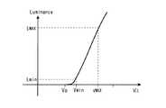
図7に、有機EL発光素子7にかける電圧VELとそのときの発光輝度の相関曲線を示す。電圧VELが一定値I0以下の間は電圧値にかかわらず全く発光しない。そして、電圧VELが一定値V0を越えると発光し、それ以降は、電圧VELが増加するに従って輝度が大きくなる。表示装置の発光素子として有機ELを用いる場合、EL発光素子が所定の輝度Lminで弱く発光するときの電流を最低電圧Vminとし、その輝度に対して例えば一定のコントラスト、例えばコントラスト100となるような輝度LMAXを最大輝度とし、この輝度に対応する電流を最大電圧VMAXとして、この電圧の間でEL発光素子にかかる電圧VELを制御して表示を行う。電圧VELを更に高く設定すれば、より強く発光させ、更にコントラストを大きく取ることも可能であるが、有機ELは、強く発光させると寿命が短くなるという特性があり、また、強く発光させるためには、より大きな電流を流す必要がある。従って、寿命、消費電流両方の観点から、その表示装置の使用環境によって求められる程度の最大輝度及びコントラストに設定される。
【0008】
図8は、図5に示したの回路図から1画素分の電源PV、駆動TFT6、EL発光素子7を抽出して示した回路図である。図から判るように、駆動TFT6と有機EL発光素子7とは、電源PVとグランドとの間に直列に接続されている。有機EL発光素子7に流れる電流IELは、電源PVから駆動トランジスタ6を介して有機EL発光素子7に供給され、そして、この電流IELは駆動トランジスタ6のゲート電圧VGを変化させることによって制御することができる。上述したように、ゲート電極にはデータ信号が入力されており、ゲート電圧VGはデータ信号に応じた値となる。図9に駆動トランジスタ6のゲート電圧VGに対するEL発光素子7の発光輝度の相関を示す。駆動トランジスタ6がp型TFTである場合が図9(a)、n型TFTである場合が図9(b)である。駆動トランジスタ6がp型TFTである場合、ゲート電圧VG=4.5Vで最大輝度LMAXとなり、ゲート電圧VGの上昇に伴って輝度が低下し、VG=6.5Vで最小輝度Lminとなる。そして、VG=8V近傍で発光がなくなる。駆動トランジスタ6がn型TFTである場合、ゲート電圧VG=3V近傍から発光し始め、ゲート電圧VGの上昇に伴って輝度が増加し、VG=4.5Vで最小輝度Lminとなり、VG=6.5Vで最大輝度LMAXとなる。
【0009】
上述のことから、有機EL発光素子7の発光輝度を制御するために、駆動トランジスタ6のゲート電圧、即ちデータ信号は、VGmin=4.5VからVGMAX=6.5Vの間の表示する階調に応じた値で出力されるように調整すればよい、ということになる。図10に有機EL表示装置に用いるデータ信号の時間変化の一例を示す。
【0010】
【発明が解決しようとする課題】
しかし、そのようなデータ信号を出力するためには、データ信号の最大値に応じて、大きな電源を設置する必要がある。データ信号は、図示しない外付けのデータ信号処理回路によって外部より入力される映像信号をゲート電圧に最適になるように信号処理して生成するが、出力すべきデータ信号の電圧が高いと、このデータ信号処理回路の駆動電圧を高くする必要があり、消費電力の増大につながっていた。
【0011】
特に、VGMAXが5Vを越えると、データ信号処理回路の耐圧を高く設計する必要があり、通常のCMOSプロセスで製造することが困難になる。従って、従来のアクティブマトリクス型自発光表示装置は、消費電力が高く、かつ、製造コストが高いという課題があった。
【0012】
そこで、本発明は、より低消費電力で動作し、かつ製造コストの低いアクティブマトリクス型自発光表示装置を得ることを目的とする。
【0013】
【課題を解決するための手段】
本発明は、上記課題を解決するために成されたものであり、行方向に延在する複数のゲート線と、列方向に延在する複数のデータ線と、前記ゲート線及び前記データ線の交点それぞれに対応して配置される選択駆動回路と、前記選択駆動回路に接続される発光素子とを有し、前記ゲート線に入力される選択信号によって前記選択駆動回路がオンし、前記データ線に入力されるデータ信号に応じた電流が前記発光素子に供給され、データ信号に応じた輝度で前記発光素子が発光するアクティブマトリクス型有機EL表示装置において、
前記選択信号のオフ電位は接地電位よりも低く、かつ前記発光素子の陰極の電位は選択信号のオフ電位よりも低い負極性の電源に接続され、前記発光素子の陽極の電位は正極性の電源に接続されているアクティブマトリクス型有機EL表示装置である。
【0014】
また、個々の画素毎に選択トランジスタ、駆動トランジスタ、発光素子を有し、前記選択トランジスタに選択信号を入力することによって、選択トランジスタをオンし、前記選択トランジスタを介してデータ信号を前記駆動トランジスタに入力し、前記駆動トランジスタを介して前記データ信号に応じた電流を前記発光素子に流し、前記データ信号に応じて前記発光素子を発光させて表示を行うアクティブマトリクス型有機EL表示装置において、前記選択信号のオフ電位は接地電位よりも低く、かつ前記発光素子の陰極の電位は選択信号のオフ電位よりも低い負極性の電源に接続され、前記発光素子の陽極の電位は正極性の電源に接続されているアクティブマトリクス型有機EL表示装置である。
【0018】
【発明の実施の形態】
図1は本発明の実施形態にかかるEL表示装置の等価回路図である。行方向に延びる複数のゲート線1が配置され、これに交差するように列方向に複数のデータ線2及び駆動線3が配置されている。ゲート線1とデータ線2とのそれぞれの交点には選択TFT4が接続されている。選択TFT4は二つのTFT4a、4bを直列に接続したダブルゲート構造であり、選択TFT4のそれぞれのTFT4a、4bのゲートはゲート線1に接続され、選択TFT4aのドレインがデータ線2に接続されている。選択TFT4bのソースは保持コンデンサ5と駆動TFT6のゲートに接続されている。駆動TFT6のドレインは、駆動線3に接続され、ソースは有機EL発光素子7の陽極に接続されている。以上は、従来のEL表示装置と同様であり、その断面図についても従来と同様である。
【0019】
本実施形態の特徴とするところは、有機EL発光素子7の陰極が接地されず、負の電圧であるシフト電圧VSHIFTを印加する電源CVに接続されている点である。図2は、図1の回路図から1画素分の陽極側電源PV、駆動TFT6、EL発光素子7及び陰極側電源CVを抽出して示した回路図である。接地電圧を基準として正の電圧を印加する電源PVと負の電圧を印加する電源CVとの間に駆動TFT6と有機EL発光素子7とが直列に接続されている。
【0020】
上述したように、適切な輝度で有機EL発光素子7を発行させるためには、従来、VGminからVGMAXの間で駆動する必要があったが、VGmin未満の電圧は、単に電圧を底上げするのみであり、階調表示にはなんら寄与していなかった。そこで、本実施形態においては、図9に示した底上げ分の電圧を極性反転し、シフト電圧VSHIFTとして負電源CVに印加している。本実施形態に置いて、電源CVの電圧、即ちシフト電圧VSHIFTは-4Vである。
【0021】
有機EL発光素子7の発光輝度は、その陽極と陰極の間の電位差によって決まる。従来のように、正電源PVと接地との間でこの電位差を与えるのではなく、正電源PVと負電源CVを併用することによって、有機EL発光素子7の駆動トランジスタ6のゲート電圧に対する発光輝度は、図9に示した相関から図3に示した相関にシフトさせることができる。これは、図9に示した電圧の底上げ分が階調表示に全く寄与していないことに着目し、その分を反転して負電圧に印加するという逆転の発想によって成されたものである。
【0022】
本実施形態の駆動トランジスタ6のゲート電圧VGと有機EL発光素子7の発光輝度の相関を図3に示す。駆動トランジスタ6がp型TFTである場合が図3(a)、n型TFTである場合が図3(b)である。駆動トランジスタ6がp型TFTである場合、ゲート電圧VG=0.5Vで最大輝度LMAXとなり、ゲート電圧VGの上昇に伴って輝度が低下し、VG=2.5Vで最小輝度Lminとなる。そして、VG=3V近傍で発光がなくなる。そして駆動トランジスタ6がn型TFTである場合は、VG=0.5Vで最小輝度Lminとなり、VG=2.5Vで最大輝度LMAXとなる。即ち、本実施形態のデータ電圧は、VGmin=0.5VからVGMAX=2. 5Vの間となるように設定すれば良く、従来に比較して、低いデータ電圧で駆動できる。従って、本実施形態は、従来よりも低消費電力で駆動することができる。また、シフト電圧VSHIFT=-4V、データ電圧の最大値VGMAX=2.5Vと、いずれの電圧も絶対値が5Vよりも小さいため、本実施形態に用いるデータ信号処理回路は、CMOSプロセスで作成することができ、製造コストを低減することができる。
【0023】
そして、シフト電圧VSHIFTは電圧の底上げ分で任意の値に設定することができ、シフト電圧VSHIFTに応じた分だけデータ信号をシフトさせることができる。本実施形態のようにVSHIFT=-4Vとしても良いし、これより小さい値としてももちろんよい。VSHIFT=-4Vを大きく取れば、それだけデータ信号をシフトさせることができ、それだけ消費電力を低減することができる。少なくとも、シフトさせた後のデータ信号の最大値が5V以下になるようにするのがよい。さらに、シフトさせた後のデータ信号の最小値VGminを0Vとできるように、本実施形態に用いたパネルであればVSHIFT=-4.5Vに設定しても良い。
【0024】
ところで、選択トランジスタ4のゲート電圧は通常オンとオフの2値で制御され、オフは、0V、オンは所定の正電圧に設定される。ところが、VGの下限VGminを0Vとなるようにシフト電圧を設定すると、データ信号がVGminとなったときに問題が生じる。即ち、データ信号が0Vであったとき、ゲート線1の選択期間が終了し、選択トランジスタ4のゲート信号がオフ、即ち0Vとなると、選択トランジスタ4において、活性層とゲート電極がともに0Vとなって電位差がなくなる。一般的にトランジスタの活性層とゲート電極との間の電位差がなくなると、チャネルにリーク電流が生じる。この問題を解決するためには、選択トランジスタ4のゲート信号は、VSHIFTに応じた負電圧と、所定の正電圧との間で変化させるようにする。そうすることによって、VGmin=0Vの時でもリーク電流が流れない。
【0025】
本実施形態において、陰極19は、図6に示したとおり、複数の画素に跨って共通で形成されている。従って、陰極19のいずれかの部分に負電源を接続すれば、本実施形態は容易に実施することができ、負電源CVを接続するにあたっては、特段のマスク変更等の大幅なコストを要するものではない。
【0026】
また、上記実施形態では、選択駆動回路として、図1に示した選択TFT4、駆動TFT6を有する回路を例示して説明したが、例えば選択TFT4をダブルゲート構造でない通常のTFT構造としたり、その他特性改善のための更なるTFTを追加するなど、任意の形態とすることができる。要は、画素毎に配置された自発光素子それぞれに対して、所定の電流を供給する回路であれば、一極性の電源と逆極性の電源との間に自発光素子を配置し、同様に実施することができる。
【0027】
【発明の効果】
以上に詳述したように、本発明によれば、発光素子が、第1の極性電圧を出力する第1の電源と、第1の極性とは逆極性の電圧を出力する第2の電源との間に接続されているので、第2の電源電圧分だけデータ信号をシフトして、低電圧化することができるので、表示装置を低消費電力化できる。
【0028】
そして、データ信号処理回路に高耐圧トランジスタを用いる必要がなく、通常のCMOSプロセスで製造でき、表示装置の製造コストを低減することができる。
【図面の簡単な説明】
【図1】本発明の一実施形態にかかる有機EL表示装置を示す回路図である。
【図2】本発明の一実施形態にかかる有機EL表示装置の一部を示す回路図である。
【図3】本発明の一実施形態における駆動TFTゲート電圧に対する有機EL素子の発光輝度を示す図である。
【図4】本発明の一実施形態におけるデータ信号の一例を示す図である。
【図5】従来の有機EL表示装置を示す回路図である。
【図6】有機EL表示装置の断面図である。
【図7】有機EL発光素子の電圧に対する発光輝度を示す図である。
【図8】従来の有機EL表示装置の一部を示す回路図である。
【図9】従来の有機EL表示装置における駆動TFTゲート電圧に対する有機EL素子の発光輝度を示す図である。
【図10】従来の有機EL表示装置のデータ信号の一例を示す図である。
【符号の説明】
1:ゲート線
2:データ線
3:駆動線
4:選択トランジスタ
5:保持コンデンサ
6:駆動トランジスタ
7:有機EL発光素子
PV:正電源
CV:負電源[0001]
BACKGROUND OF THE INVENTION
The present invention relates to an active matrix self-luminous display device having self-luminous elements arranged independently for each pixel by a selective driving circuit composed of a thin film transistor (TFT) or the like, and more particularly to an active matrix organic electroluminescent display device. The present invention relates to a luminescence (Electro Luminescence; EL) display device.
[0002]
[Prior art]
Since self-luminous display devices have lower power consumption and smaller size than CRTs and do not have a viewing angle dependency like LCDs, EL display devices using EL elements have recently been replaced with CRTs and LCDs. It is attracting attention as a device. For example, an EL display device including a TFT as a switching element for driving the EL element is being developed.
[0003]
FIG. 5 shows an equivalent circuit diagram of the organic EL display device. A plurality of gate lines 1 extending in the row direction are arranged, and a plurality of
[0004]
The gate line 1 is connected to a gate line driver (not shown), and gate signals are sequentially applied to the gate line 1 by the gate line driver. The gate signal is a binary signal that is turned on or off, and is a positive predetermined voltage when turned on and 0 V when turned off. The gate line driver turns on the gate signal of a predetermined gate line selected from among the plurality of gate lines 1 connected. When the gate signal is turned on, the TFTs of all the
[0005]
The above is the operation principle of the active matrix organic EL display device. In this specification, the
[0006]
FIG. 6 is a sectional view of an active matrix organic EL display device. A plurality of driving
[0007]
FIG. 7 shows a correlation curve between the voltage VEL applied to the organic EL light emitting element 7 and the light emission luminance at that time. While the voltage VEL is lower than the constant value I0, no light is emitted regardless of the voltage value. When the voltage VEL exceeds a certain value V0, light is emitted, and thereafter, the luminance increases as the voltage VEL increases. When an organic EL is used as the light emitting element of the display device, the current when the EL light emitting element emits light weakly at a predetermined luminance Lmin is set to the minimum voltage Vmin, and for example, a constant contrast with respect to the luminance, for example, contrast 100 The luminance LMAX is set to the maximum luminance, and the current corresponding to the luminance is set to the maximum voltage VMAX , and the voltage VEL applied to the EL light emitting element is controlled between the voltages to perform display. If the voltage VEL is set higher, it is possible to emit light more strongly and increase the contrast. However, organic EL has the characteristic that the lifetime is shortened if it emits strongly, and it also emits strongly. Requires a larger current to flow. Therefore, the maximum brightness and contrast are set to the extent required by the usage environment of the display device from the viewpoint of both life and current consumption.
[0008]
FIG. 8 is a circuit diagram in which the power source PV, the driving
[0009]
From the above, in order to control the light emission luminance of the organic EL light emitting element 7, the gate voltage of the
[0010]
[Problems to be solved by the invention]
However, in order to output such a data signal, it is necessary to install a large power source according to the maximum value of the data signal. The data signal is generated by performing signal processing on the video signal input from the outside by an external data signal processing circuit (not shown) so as to be optimal for the gate voltage. When the voltage of the data signal to be output is high, The drive voltage of the data signal processing circuit needs to be increased, leading to an increase in power consumption.
[0011]
In particular, when VGMAX exceeds 5V, it is necessary to design the data signal processing circuit with a high withstand voltage, which makes it difficult to manufacture with a normal CMOS process. Therefore, the conventional active matrix self-luminous display device has the problems of high power consumption and high manufacturing cost.
[0012]
Therefore, an object of the present invention is to obtain an active matrix self-luminous display device that operates with lower power consumption and has a low manufacturing cost.
[0013]
[Means for Solving the Problems]
The present invention has been made to solve the above problems, and includes a plurality of gate lines extending in a row direction, a plurality of data lines extending in a column direction, the gate lines and the data lines. A selection drive circuit disposed corresponding to each of the intersections; and a light emitting element connected to the selection drive circuit. The selection drive circuit is turned on by a selection signal input to the gate line, and the data line In an active matrix organic EL display device in which a current corresponding to a data signal input to the light emitting element is supplied to the light emitting element, and the light emitting element emits light with a luminance corresponding to the data signal.
The off potential of the selection signal is lower than the ground potential, and the cathode potential of the light emitting element is connected to a negative power source that is lower than the off potential of the selection signal, and the anode potential of the light emitting element is a positive power source. It is an active matrix type organic EL display device connected to.
[0014]
Each pixel has a selection transistor, a driving transistor, and a light emitting element. By inputting a selection signal to the selection transistor, the selection transistor is turned on, and a data signal is transmitted to the driving transistor through the selection transistor. In the active matrix organic EL display device that performs display by causing a current corresponding to the data signal to flow through the light emitting element through the driving transistor and causing the light emitting element to emit light according to the data signal. The signal off potential is lower than the ground potential, and the cathode potential of the light emitting element is connected to a negative power source that is lower than the off potential of the selection signal, and the anode potential of the light emitting element is connected to a positive power source. This is an active matrix organic EL display device.
[0018]
DETAILED DESCRIPTION OF THE INVENTION
FIG. 1 is an equivalent circuit diagram of an EL display device according to an embodiment of the present invention. A plurality of gate lines 1 extending in the row direction are arranged, and a plurality of
[0019]
The feature of this embodiment is that the cathode of the organic EL light-emitting element 7 is not grounded and is connected to a power source CV that applies a shift voltage VSHIFT which is a negative voltage. FIG. 2 is a circuit diagram in which the anode side power source PV, the driving
[0020]
As described above, in order to issue the organic EL light emitting element 7 with appropriate luminance, it has been conventionally necessary to drive between VGmin and VGMAX , but a voltagelower than VGmin simplyraises the voltage. It did not contribute to the gradation display. Therefore, in the present embodiment, the polarity of the raised voltage shown in FIG. 9 is inverted and applied to the negative power source CV as the shift voltage VSHIFT . In this embodiment, the voltage of the power source CV, that is, the shift voltage VSHIFT is −4V.
[0021]
The light emission luminance of the organic EL light emitting element 7 is determined by the potential difference between the anode and the cathode. Instead of giving this potential difference between the positive power source PV and the ground as in the prior art, the light emission luminance with respect to the gate voltage of the
[0022]
FIG. 3 shows the correlation between the gate voltage VG of the driving
[0023]
The shift voltage VSHIFT can be set to an arbitrary value by increasing the voltage, and the data signal can be shifted by an amount corresponding to the shift voltage VSHIFT . As in this embodiment, VSHIFT = −4 V may be used, or a value smaller than this may be used. If VSHIFT = -4V is set large, the data signal can be shifted by that amount, and the power consumption can be reduced accordingly. It is preferable that at least the maximum value of the data signal after the shift is 5 V or less. Furthermore, VSHIFT = −4.5V may be set in the panel used in this embodiment so that the minimum value VGmin of the data signal after the shift can be set to 0V.
[0024]
By the way, the gate voltage of the
[0025]
In the present embodiment, the
[0026]
In the above-described embodiment, the circuit having the
[0027]
【The invention's effect】
As described in detail above, according to the present invention, the light-emitting element includes a first power source that outputs a first polarity voltage, and a second power source that outputs a voltage having a polarity opposite to the first polarity. Since the data signal can be shifted by the amount corresponding to the second power supply voltage to reduce the voltage, the display device can reduce power consumption.
[0028]
Further, it is not necessary to use a high voltage transistor in the data signal processing circuit, and the data signal processing circuit can be manufactured by a normal CMOS process, and the manufacturing cost of the display device can be reduced.
[Brief description of the drawings]
FIG. 1 is a circuit diagram showing an organic EL display device according to an embodiment of the present invention.
FIG. 2 is a circuit diagram showing a part of an organic EL display device according to an embodiment of the present invention.
FIG. 3 is a diagram showing light emission luminance of an organic EL element with respect to a driving TFT gate voltage in an embodiment of the present invention.
FIG. 4 is a diagram showing an example of a data signal in an embodiment of the present invention.
FIG. 5 is a circuit diagram showing a conventional organic EL display device.
FIG. 6 is a cross-sectional view of an organic EL display device.
FIG. 7 is a diagram showing light emission luminance with respect to voltage of an organic EL light emitting device.
FIG. 8 is a circuit diagram showing a part of a conventional organic EL display device.
FIG. 9 is a diagram showing light emission luminance of an organic EL element with respect to a driving TFT gate voltage in a conventional organic EL display device.
FIG. 10 is a diagram illustrating an example of a data signal of a conventional organic EL display device.
[Explanation of symbols]
1: Gate line 2: Data line 3: Drive line 4: Select transistor 5: Holding capacitor 6: Drive transistor 7: Organic EL light emitting element
PV: Positive power supply
CV: Negative power supply
Claims (2)
Translated fromJapanese前記選択信号のオフ電位は接地電位よりも低く、かつ前記発光素子の陰極の電位は選択信号のオフ電位よりも低い負極性の電源に接続され、前記発光素子の陽極の電位は正極性の電源に接続されていることを特徴とするアクティブマトリクス型有機EL表示装置。A plurality of gate lines extending in a row direction; a plurality of data lines extending in a column direction; a selection drive circuit disposed corresponding to each intersection of the gate lines and the data lines; and the selection drive circuit The selection driving circuit is turned on by a selection signal input to the gate line, and a current corresponding to the data signal input to the data line is supplied to the light emitting element. In the active matrix organic EL display device in which the light emitting element emits light with luminance according to a data signal,
The off potential of the selection signal is lower than a ground potential, and the cathode potential of the light emitting element is connected to a negative power source lower than the off potential of the selection signal, and the anode potential of the light emitting element is a positive power source. An active matrix organic EL display device characterized by being connected to.
前記選択トランジスタに選択信号を入力することによって、選択トランジスタをオンし、前記選択トランジスタを介してデータ信号を前記駆動トランジスタに入力し、前記駆動トランジスタを介して前記データ信号に応じた電流を前記発光素子に流し、前記データ信号に応じて前記発光素子を発光させて表示を行うアクティブマトリクス型有機EL表示装置において、
前記選択信号のオフ電位は接地電位よりも低く、かつ前記発光素子の陰極の電位は選択信号のオフ電位よりも低い負極性の電源に接続され、前記発光素子の陽極の電位は正極性の電源に接続されていることを特徴とするアクティブマトリクス型有機EL表示装置。Each pixel has a selection transistor, a drive transistor, and a light emitting element.
By inputting a selection signal to the selection transistor, the selection transistor is turned on, a data signal is input to the driving transistor through the selection transistor, and a current corresponding to the data signal is emitted through the driving transistor. In an active matrix organic EL display device that displays an image by causing the light emitting element to emit light according to the data signal,
The off potential of the selection signal is lower than a ground potential, and the cathode potential of the light emitting element is connected to a negative power source lower than the off potential of the selection signal, and the anode potential of the light emitting element is a positive power source. An active matrix organic EL display device characterized by being connected to.
Priority Applications (7)
| Application Number | Priority Date | Filing Date | Title |
|---|---|---|---|
| JP2000231854AJP3670941B2 (en) | 2000-07-31 | 2000-07-31 | Active matrix self-luminous display device and active matrix organic EL display device |
| TW090118397ATW514864B (en) | 2000-07-31 | 2001-07-27 | Active matrix type self-luminous display device and active matrix type organic EL display device |
| KR10-2001-0045936AKR100461482B1 (en) | 2000-07-31 | 2001-07-30 | Active matrix type self-luminescent display device and active matrix type organic el display device |
| US09/918,960US6509692B2 (en) | 2000-07-31 | 2001-07-31 | Self-emissive display device of active matrix type and organic EL display device of active matrix type |
| EP01306584AEP1178463B1 (en) | 2000-07-31 | 2001-07-31 | Self-emissive display device of active matrix type and organic EL display device of active matrix type |
| CNB01124755XACN1244085C (en) | 2000-07-31 | 2001-07-31 | Active matrix type self-luminous display device and active matrix type organic EL display device |
| DE60123344TDE60123344T2 (en) | 2000-07-31 | 2001-07-31 | Active matrix self-emitting display and active matrix organic electroluminescent display |
Applications Claiming Priority (1)
| Application Number | Priority Date | Filing Date | Title |
|---|---|---|---|
| JP2000231854AJP3670941B2 (en) | 2000-07-31 | 2000-07-31 | Active matrix self-luminous display device and active matrix organic EL display device |
Publications (2)
| Publication Number | Publication Date |
|---|---|
| JP2002040963A JP2002040963A (en) | 2002-02-08 |
| JP3670941B2true JP3670941B2 (en) | 2005-07-13 |
Family
ID=18724627
Family Applications (1)
| Application Number | Title | Priority Date | Filing Date |
|---|---|---|---|
| JP2000231854AExpired - LifetimeJP3670941B2 (en) | 2000-07-31 | 2000-07-31 | Active matrix self-luminous display device and active matrix organic EL display device |
Country Status (7)
| Country | Link |
|---|---|
| US (1) | US6509692B2 (en) |
| EP (1) | EP1178463B1 (en) |
| JP (1) | JP3670941B2 (en) |
| KR (1) | KR100461482B1 (en) |
| CN (1) | CN1244085C (en) |
| DE (1) | DE60123344T2 (en) |
| TW (1) | TW514864B (en) |
Families Citing this family (45)
| Publication number | Priority date | Publication date | Assignee | Title |
|---|---|---|---|---|
| JP2000163014A (en)* | 1998-11-27 | 2000-06-16 | Sanyo Electric Co Ltd | Electroluminescence display device |
| EP3716257B1 (en) | 2001-09-07 | 2021-01-20 | Joled Inc. | El display panel, method of driving the same, and el display device |
| US11302253B2 (en) | 2001-09-07 | 2022-04-12 | Joled Inc. | El display apparatus |
| KR20030038522A (en)* | 2001-11-09 | 2003-05-16 | 산요 덴키 가부시키가이샤 | Display apparatus with function for initializing luminance data of optical element |
| JP3800404B2 (en)* | 2001-12-19 | 2006-07-26 | 株式会社日立製作所 | Image display device |
| GB0130411D0 (en)* | 2001-12-20 | 2002-02-06 | Koninkl Philips Electronics Nv | Active matrix electroluminescent display device |
| JP2003255899A (en)* | 2001-12-28 | 2003-09-10 | Sanyo Electric Co Ltd | Display device |
| JP3953330B2 (en) | 2002-01-25 | 2007-08-08 | 三洋電機株式会社 | Display device |
| JP3723507B2 (en) | 2002-01-29 | 2005-12-07 | 三洋電機株式会社 | Driving circuit |
| JP2003308030A (en) | 2002-02-18 | 2003-10-31 | Sanyo Electric Co Ltd | Display device |
| JP2003332058A (en) | 2002-03-05 | 2003-11-21 | Sanyo Electric Co Ltd | Electroluminescent panel and method of manufacturing the same |
| JP3671012B2 (en)* | 2002-03-07 | 2005-07-13 | 三洋電機株式会社 | Display device |
| CN100517422C (en) | 2002-03-07 | 2009-07-22 | 三洋电机株式会社 | Wiring structure, manufacturing method thereof, and optical device |
| JP3837344B2 (en) | 2002-03-11 | 2006-10-25 | 三洋電機株式会社 | Optical element and manufacturing method thereof |
| TW594617B (en)* | 2002-03-13 | 2004-06-21 | Sanyo Electric Co | Organic EL display panel and method for making the same |
| KR100432651B1 (en)* | 2002-06-18 | 2004-05-22 | 삼성에스디아이 주식회사 | An image display apparatus |
| JP4120326B2 (en)* | 2002-09-13 | 2008-07-16 | ソニー株式会社 | Current output type driving circuit and display device |
| TW564390B (en)* | 2002-09-16 | 2003-12-01 | Au Optronics Corp | Driving circuit and method for light emitting device |
| JP3949040B2 (en)* | 2002-09-25 | 2007-07-25 | 東北パイオニア株式会社 | Driving device for light emitting display panel |
| KR100911205B1 (en)* | 2002-12-31 | 2009-08-06 | 엘지디스플레이 주식회사 | Active matrix display |
| CN1310204C (en)* | 2003-01-09 | 2007-04-11 | 友达光电股份有限公司 | organic light emitting display |
| US7253812B2 (en) | 2003-02-12 | 2007-08-07 | Sanyo Electric Co., Ltd. | El display driver and El display |
| CN1312650C (en)* | 2003-04-03 | 2007-04-25 | 胜华科技股份有限公司 | Method and device for image uniformity of active organic light emitting diode display |
| TWI464730B (en)* | 2003-04-29 | 2014-12-11 | Samsung Electronics Co Ltd | Gate driving circuit and display apparatus having the same |
| US7369111B2 (en) | 2003-04-29 | 2008-05-06 | Samsung Electronics Co., Ltd. | Gate driving circuit and display apparatus having the same |
| US7256758B2 (en)* | 2003-06-02 | 2007-08-14 | Au Optronics Corporation | Apparatus and method of AC driving OLED |
| KR100520827B1 (en)* | 2003-06-21 | 2005-10-12 | 엘지.필립스 엘시디 주식회사 | Apparatus and method for driving of electro luminescence display panel and method for fabrication of electro luminescence display device |
| KR100552968B1 (en)* | 2003-09-23 | 2006-02-15 | 삼성에스디아이 주식회사 | Active Matrix Organic Light Emitting Display |
| US7683860B2 (en)* | 2003-12-02 | 2010-03-23 | Semiconductor Energy Laboratory Co., Ltd. | Display device, driving method thereof, and element substrate |
| US20050184407A1 (en)* | 2004-02-20 | 2005-08-25 | Takahiro Korenari | Transistor circuit, thin film transistor circuit and display device |
| EP1591992A1 (en)* | 2004-04-27 | 2005-11-02 | Thomson Licensing, S.A. | Method for grayscale rendition in an AM-OLED |
| TWI243625B (en)* | 2004-05-04 | 2005-11-11 | Toppoly Optoelectronics Corp | Organic light-emitting display structure |
| US7391394B2 (en)* | 2004-05-21 | 2008-06-24 | Au Optronics Corporation | Electroluminescent display |
| JP4941911B2 (en)* | 2004-11-29 | 2012-05-30 | ローム株式会社 | Organic EL drive circuit and organic EL display device using the same |
| JP5084111B2 (en)* | 2005-03-31 | 2012-11-28 | 三洋電機株式会社 | Display device and driving method of display device |
| KR100712293B1 (en) | 2005-05-24 | 2007-04-27 | 삼성에스디아이 주식회사 | Panel of organic light emitting display device and organic light emitting display device comprising same |
| KR100665943B1 (en)* | 2005-06-30 | 2007-01-09 | 엘지.필립스 엘시디 주식회사 | Organic electroluminescent display device and driving method |
| KR100635502B1 (en) | 2005-08-12 | 2006-10-17 | 삼성에스디아이 주식회사 | Organic light emitting display device |
| TWI271115B (en)* | 2005-08-30 | 2007-01-11 | Au Optronics Corp | Active display and driving circuit of a pixel thereof |
| JP2009014796A (en)* | 2007-06-30 | 2009-01-22 | Sony Corp | El display panel, power supply line driving device and electronic equipment |
| US9111483B2 (en)* | 2011-12-23 | 2015-08-18 | Semiconductor Energy Laboratory Co., Ltd. | Display device |
| JP5770236B2 (en)* | 2013-09-18 | 2015-08-26 | 株式会社ジャパンディスプレイ | Display device |
| US9953570B2 (en) | 2014-02-05 | 2018-04-24 | Joled Inc. | Display device |
| CN103971636A (en) | 2014-04-22 | 2014-08-06 | 上海和辉光电有限公司 | Active Matrix Organic Light Emitting Diode Driving Circuit |
| JP6715312B2 (en)* | 2018-12-04 | 2020-07-01 | 三星ディスプレイ株式會社Samsung Display Co.,Ltd. | Display device |
Family Cites Families (13)
| Publication number | Priority date | Publication date | Assignee | Title |
|---|---|---|---|---|
| US5598180A (en) | 1992-03-05 | 1997-01-28 | Kabushiki Kaisha Toshiba | Active matrix type display apparatus |
| US5684365A (en)* | 1994-12-14 | 1997-11-04 | Eastman Kodak Company | TFT-el display panel using organic electroluminescent media |
| US6462722B1 (en) | 1997-02-17 | 2002-10-08 | Seiko Epson Corporation | Current-driven light-emitting display apparatus and method of producing the same |
| US6023259A (en)* | 1997-07-11 | 2000-02-08 | Fed Corporation | OLED active matrix using a single transistor current mode pixel design |
| US5933066A (en) | 1997-11-13 | 1999-08-03 | Eaton Corporation | Circuit interrupter with terminal shield and wire trough |
| EP1055218A1 (en) | 1998-01-23 | 2000-11-29 | Fed Corporation | High resolution active matrix display system on a chip with high duty cycle for full brightness |
| TW439387B (en)* | 1998-12-01 | 2001-06-07 | Sanyo Electric Co | Display device |
| US6366025B1 (en)* | 1999-02-26 | 2002-04-02 | Sanyo Electric Co., Ltd. | Electroluminescence display apparatus |
| JP2000259124A (en)* | 1999-03-05 | 2000-09-22 | Sanyo Electric Co Ltd | Electroluminescence display device |
| US6421033B1 (en)* | 1999-09-30 | 2002-07-16 | Innovative Technology Licensing, Llc | Current-driven emissive display addressing and fabrication scheme |
| US6587086B1 (en) | 1999-10-26 | 2003-07-01 | Semiconductor Energy Laboratory Co., Ltd. | Electro-optical device |
| US6278242B1 (en)* | 2000-03-20 | 2001-08-21 | Eastman Kodak Company | Solid state emissive display with on-demand refresh |
| US6396217B1 (en)* | 2000-12-22 | 2002-05-28 | Visteon Global Technologies, Inc. | Brightness offset error reduction system and method for a display device |
- 2000
- 2000-07-31JPJP2000231854Apatent/JP3670941B2/ennot_activeExpired - Lifetime
- 2001
- 2001-07-27TWTW090118397Apatent/TW514864B/ennot_activeIP Right Cessation
- 2001-07-30KRKR10-2001-0045936Apatent/KR100461482B1/ennot_activeCeased
- 2001-07-31CNCNB01124755XApatent/CN1244085C/ennot_activeExpired - Lifetime
- 2001-07-31EPEP01306584Apatent/EP1178463B1/ennot_activeExpired - Lifetime
- 2001-07-31DEDE60123344Tpatent/DE60123344T2/ennot_activeExpired - Lifetime
- 2001-07-31USUS09/918,960patent/US6509692B2/ennot_activeExpired - Lifetime
Also Published As
| Publication number | Publication date |
|---|---|
| EP1178463B1 (en) | 2006-09-27 |
| EP1178463A2 (en) | 2002-02-06 |
| EP1178463A3 (en) | 2002-04-24 |
| KR20020010869A (en) | 2002-02-06 |
| US6509692B2 (en) | 2003-01-21 |
| DE60123344T2 (en) | 2007-08-02 |
| CN1244085C (en) | 2006-03-01 |
| CN1341915A (en) | 2002-03-27 |
| KR100461482B1 (en) | 2004-12-14 |
| US20020021096A1 (en) | 2002-02-21 |
| TW514864B (en) | 2002-12-21 |
| JP2002040963A (en) | 2002-02-08 |
| DE60123344D1 (en) | 2006-11-09 |
Similar Documents
| Publication | Publication Date | Title |
|---|---|---|
| JP3670941B2 (en) | Active matrix self-luminous display device and active matrix organic EL display device | |
| US20210280131A1 (en) | Display apparatus | |
| US10453387B2 (en) | Display panel, display device, pixel driving circuit, and control method for the same | |
| KR100489272B1 (en) | Organic electroluminescence device and method for driving the same | |
| TWI395169B (en) | Display device | |
| US11935467B2 (en) | OLED display panel and display device | |
| CN110600486B (en) | Display device, method of manufacturing the same, and electronic apparatus | |
| CN101800025B (en) | Driving method of organic electroluminescent light-emitting part | |
| JP2000267628A (en) | Active el display device | |
| KR102786557B1 (en) | Pixel and display device including the same | |
| JP2000259098A (en) | Active el display device | |
| JP7253796B2 (en) | Pixel circuit and display device | |
| JP7316655B2 (en) | Pixel circuit and display device | |
| CN112753064B (en) | display device | |
| JP2012118381A (en) | Organic el display divice and driving method thereof | |
| CN115472126A (en) | Pixel circuit, driving method thereof, display substrate and display device | |
| JP2004126106A (en) | Electroluminescence display device | |
| KR100543838B1 (en) | Electroluminesence display device | |
| JP2012237931A (en) | Active matrix type organic light-emitting display device | |
| JP3671012B2 (en) | Display device | |
| TWI514351B (en) | Pixel driving circuit and display device | |
| JP2003280576A (en) | Active matrix type organic el display | |
| CN100590905C (en) | Organic light emitting diode device including brightness compensation plate | |
| KR20080054189A (en) | Organic light emitting display device | |
| CN100397461C (en) | Driving method of display |
Legal Events
| Date | Code | Title | Description |
|---|---|---|---|
| A02 | Decision of refusal | Free format text:JAPANESE INTERMEDIATE CODE: A02 Effective date:20031202 | |
| A521 | Request for written amendment filed | Free format text:JAPANESE INTERMEDIATE CODE: A523 Effective date:20050224 | |
| A61 | First payment of annual fees (during grant procedure) | Free format text:JAPANESE INTERMEDIATE CODE: A61 Effective date:20050415 | |
| R151 | Written notification of patent or utility model registration | Ref document number:3670941 Country of ref document:JP Free format text:JAPANESE INTERMEDIATE CODE: R151 | |
| FPAY | Renewal fee payment (event date is renewal date of database) | Free format text:PAYMENT UNTIL: 20090422 Year of fee payment:4 | |
| FPAY | Renewal fee payment (event date is renewal date of database) | Free format text:PAYMENT UNTIL: 20090422 Year of fee payment:4 | |
| FPAY | Renewal fee payment (event date is renewal date of database) | Free format text:PAYMENT UNTIL: 20100422 Year of fee payment:5 | |
| FPAY | Renewal fee payment (event date is renewal date of database) | Free format text:PAYMENT UNTIL: 20110422 Year of fee payment:6 | |
| FPAY | Renewal fee payment (event date is renewal date of database) | Free format text:PAYMENT UNTIL: 20120422 Year of fee payment:7 | |
| FPAY | Renewal fee payment (event date is renewal date of database) | Free format text:PAYMENT UNTIL: 20130422 Year of fee payment:8 | |
| FPAY | Renewal fee payment (event date is renewal date of database) | Free format text:PAYMENT UNTIL: 20140422 Year of fee payment:9 | |
| R250 | Receipt of annual fees | Free format text:JAPANESE INTERMEDIATE CODE: R250 | |
| EXPY | Cancellation because of completion of term |