JP3670918B2 - Image processing device - Google Patents
Image processing deviceDownload PDFInfo
- Publication number
- JP3670918B2 JP3670918B2JP35989099AJP35989099AJP3670918B2JP 3670918 B2JP3670918 B2JP 3670918B2JP 35989099 AJP35989099 AJP 35989099AJP 35989099 AJP35989099 AJP 35989099AJP 3670918 B2JP3670918 B2JP 3670918B2
- Authority
- JP
- Japan
- Prior art keywords
- image data
- image
- processing
- unit
- control unit
- Prior art date
- Legal status (The legal status is an assumption and is not a legal conclusion. Google has not performed a legal analysis and makes no representation as to the accuracy of the status listed.)
- Expired - Fee Related
Links
Images


Landscapes
- Facsimiles In General (AREA)
Description
Translated fromJapanese【0001】
【発明の属する技術分野】
この発明は、ディジタル画像データに対する画像処理、特に、複写機、ファクシミリ、プリンター、スキャナー等の機能を複合したディジタル複合機における画像データに対する画像処理をおこなう画像処理装置に関する。
【0002】
【従来の技術】
従来、アナログ複写機からディジタル化された画像データの処理をおこなうディジタル複写機が登場し、さらに、ディジタル複写機が複写機としての機能だけでなく、複写機の機能に加えて、ファクシミリの機能、プリンターの機能、スキャナーの機能等の各機能を複合したディジタル複合機が存在する。
【0003】
図12は、従来技術にかかるディジタル複合機のハードウエア構成を示すブロック図である。図12に示すように、ディジタル複合機は、読み取りユニット1201、画像処理ユニット1202、ビデオ制御部1203、書き込みユニット1204の一連の各構成部、さらにはメモリー制御ユニット1205およびメモリー・モジュール1206によって形成される複写機を構成する部分(複写機部分)と、バス制御等をおこなうマザーボード1211を介して、追加的にファクシミリ制御ユニット1212、プリンター制御ユニット1213、スキャナー制御ユニット1214等のユニットが接続されることによって、ディジタル複合機としての各機能を実現していた。
【0004】
したがって、複写機としての機能を実現する複写機部分は、読み取りユニット1201、画像処理ユニット1202、ビデオ制御部1203、書き込みユニット1204の各構成部は、システム・コントローラー1207、RAM1208、ROM1209によって各構成部の一連の動作が制御されているのに対し、ファクシミリ制御ユニット1212、プリンター制御ユニット1213、スキャナー制御ユニット1214等の各ユニットは、複写機における確立された一連の動作の一部を利用することにより各ユニットの機能を実現するものであった。
【0005】
換言すると、上記一連の構成部による一つのシステムとして確立している複写機部分にファクシミリ制御ユニット1212、プリンター制御ユニット1213、スキャナー制御ユニット1214をアドオンすることにより、ディジタル複合機の機能を実現するものであった。これは、上記一連の構成部をASIC(Application Specific Integrated Circuit)等のハードウエアにより構成することにより、処理速度を重視する(処理の高速化を図る)という背景によるものであった。
【0006】
また、読み取り信号の画像処理、メモリーへの画像蓄積、複数機能の並行動作およびそれぞれの画像処理を最適化する『画像処理装置』(たとえば、特開平8−274986号公報)等が開示されており、各種の画像処理を一つの画像処理構成で実行できるものがあった。
【0007】
【発明が解決しようとする課題】
しかしながら、上記従来技術におけるディジタル複合機においては、上述のとおり複写機部分が一つのシステムとして確立していることから、ファクシミリ制御ユニット1212、プリンター制御ユニット1213、スキャナー制御ユニット1214等、上記複写機部分に接続されたユニットについては、各機能を実現するために複写機部分とは別個に、それぞれ独立してシステムを構築しなければならないという問題点があった。
【0008】
したがって、各制御ユニットの機能を実現するために必要なメモリー・モジュールは各ユニットがそれぞれ備えるように構成しなければならない。そのため、各ユニットが複写機部分の備えているメモリー・モジュール1206を有効に活用できないばかりか、各ユニットごとに重複したメモリー・モジュールを備えることによる装置全体としてのサイズの増大化、コストの増大化を招いてしまうという問題点があった。
【0009】
また同様に、上記複写機部分が一つのシステムとして確立していることから、周辺ユニットの性能向上にともなう機能向上が効率よく図れないという問題点があった。読み取りユニット1201や書き込みユニット1204のみを変更したい場合、より具体的には、400dpiであった読取ユニット1201あるいは書込ユニット1204を600dpiのものに変更したい場合に、単にユニットの交換のみの作業では装置全体の機能向上を容易におこなうことができないという問題点があった。
【0010】
すなわち、上記複写機部分全体としてすでに400dpiによって読み取り/書き込みされるように一連のシステムが確立されてしまっているため、上記のようなユニットを変換する場合は、中間処理のためのマトリクスサイズやしきい値等を変更する必要がある。また、他のユニットについても、600dpiによる読み取り/書き込みができるようにその設定内容を変更しなければならない場合がある。
【0011】
したがって、ASIC等のハードウエアで構成されている場合は、ハードウエア(カスタム化したICやLSI等)そのものを交換しなければならない。それゆえに、周辺ユニットの性能の向上にともない、周辺ユニットを交換するだけでは、装置全体の機能を容易に向上させることができないのである。
【0012】
また、マザーボード1211を介して各機能ユニットをアドオンするような従来のディジタル複合機や、各機能ユニットを必要に応じて組み合わせるようなモジュール化されたディジタル複合機については、画像データの送受信の制御をうまくおこなうことができない場合があるという問題点があった。
【0013】
すなわち、各機能ユニット間で画像データの送受信をおこなうためには、各ユニット間で共通に使用されるバス(画像データバス)を設ける必要が生じる。ここで、各機能ユニットにおいては、デバイスが動作を開始すると、画像データの送受信を中止することができない場合が多い。特にメモリー資源の有効活用を目的として、画像データを保存するメモリー・モジュールを別途設けるユニット構成とする場合は、各ユニットにおいて画像データの送受信を中止することができなくなる。
【0014】
したがって、画像データの送受信に使用されるバスを構築する際には、予め想定される複数デバイスの最大同時動作からバスの速度やバス幅を決定し、画像処理装置全体として効率的な画像データの送受信をおこなうことが必要となる。しかしながら、ディジタル複合機を各機能ごとにモジュール化する場合にあっては、各機能モジュールのバージョンアップにより、当初想定していた最大同時動作をこえてしまい、画像データの送受信をうまくおこなえなくなる場合があるという問題点があった。
【0015】
さらに、複写機を構成する部分が一つのシステムとして確立していることから、ディジタル複合機を単体スキャナーあるいは単体プリンターとして活用する場合の機能分割を容易におこなうことができないという問題点があった。
【0016】
以上のように、従来のディジタル複合機にあっては、モジュール等の共有化、ユニットごとの交換による機能向上、複数機能の分割等、システムにおける各資源の有効活用を図るという点で最適な制御構成が構築されていないという問題点があった。
【0017】
この発明は、上述した従来技術による問題点を解消するため、多機能を実現する際のシステムにおける各資源の有効活用を図り、システム全体として最適な画像データの送受信の制御が可能な画像処理装置を提供することを目的とする。
【0018】
【課題を解決するための手段】
上述した課題を解決し、目的を達成するため、この発明にかかる画像処理装置は、画像データを読み取る画像読取ユニットおよび/または画像データに対し加工編集等の画像処理を施す画像処理ユニットおよび/または画像データを転写紙等に書き込む画像書込ユニット、および、画像メモリーを制御して画像データの書込み/読出しをおこなう画像メモリー制御ユニットに接続し、接続された各ユニットとの間で画像データの送受信の制御をおこなう送受信制御手段を有する画像データ制御ユニットを備えた画像処理装置において、前記画像データ制御ユニットから画像データを送信する送信先ユニットにおいて当該画像データを処理できるか否かを判断する判断手段と、画像データを前記画像データ制御ユニットから前記送信先ユニットへ直接送信する第1の送信手段と、画像データを前記画像データ制御ユニットから前記画像メモリー制御ユニットへ順序付けをおこなって送信する第2の送信手段と、前記第1の送信手段と第2の送信手段とを切り替える切替手段と、を備え、前記送受信制御手段が、前記切替手段を制御して、前記判断手段により画像データが処理可能であると判断された場合には前記第1の送信手段に当該画像データを送信し、前記判断手段により画像データが処理不可能であると判断された場合には前記第2の送信手段に当該画像データを送信することを特徴とする。
【0019】
この発明によれば、画像データの処理待ちが必要な場合は当該画像データを画像メモリーへ送信し、処理待ちが必要でない場合は当該画像データを送信先の機能ユニットに直接送信することができる。
【0020】
また、この発明にかかる画像処理装置は、上記発明において、前記画像データ制御ユニットが、当該画像データ制御ユニットにより受信される画像データを一時格納する受信バッファーと、当該画像データ制御ユニットにより送信される画像データを一時格納する送信バッファーと、を備え、前記送受信制御手段が、前記送信バッファーおよび受信バッファーを制御して、前記送信バッファーから出力される画像データを前記受信バッファーに入力し、前記受信バッファーから出力される当該画像データを前記送信バッファーに入力することを特徴とする。
【0021】
この発明によれば、処理待ちが必要な画像データを画像メモリーに送信することなく、画像データ制御部で保持することができる。
【0022】
また、この発明にかかる画像処理装置は、上記発明において、前記送受信制御手段の制御内容を記録する記録手段と、前記記録手段を書き換える書換手段と、を備えたことを特徴とする。
【0023】
この発明によれば、画像処理装置の装置規模に応じて画像データの転送制御の内容を変更することができる。
【0024】
【発明の実施の形態】
以下に添付図面を参照して、この発明にかかる画像処理装置の好適な実施の形態を詳細に説明する。
【0025】
〔実施の形態1〕
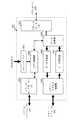
まず、本実施の形態にかかる画像処理装置の原理について説明する。図1は、この発明の本実施の形態にかかる画像処理装置の構成を機能的に示すブロック図である。図1において、画像処理装置は、以下に示す5つのユニットを含む構成である。
【0026】
上記5つのユニットとは、画像データ制御ユニット100と、画像データを読み取る画像読取ユニット101と、画像を蓄積する画像メモリーを制御して画像データの書込み/読出しをおこなう画像メモリー制御ユニット102と、画像データに対し加工編集等の画像処理を施す画像処理ユニット103と、画像データを転写紙等に書き込む画像書込ユニット104と、である。
【0027】
上記各ユニットは、画像データ制御ユニット100を中心に、画像読取ユニット101と、画像メモリー制御ユニット102と、画像処理ユニット103と、画像書込ユニット104とがそれぞれ画像データ制御ユニット100に接続されている。
【0028】
(画像データ制御ユニット100)
画像データ制御ユニット100によりおこなわれる処理としては以下のようなものがある。
【0029】
たとえば、
(1)データのバス転送効率を向上させるためのデータ圧縮処理(一次圧縮)、
(2)一次圧縮データの画像データへの転送処理、
(3)画像合成処理(複数ユニットからの画像データを合成することが可能である。また、データバス上での合成も含む。)、
(4)画像シフト処理(主走査および副走査方向の画像のシフト)、
(5)画像領域拡張処理(画像領域を周辺へ任意量だけ拡大することが可能)、
(6)画像変倍処理(たとえば、50%または200%の固定変倍)、
(7)パラレルバス・インターフェース処理、
(8)シリアルバス・インターフェース処理(後述するプロセス・コントローラー211とのインターフェース)、
(9)パラレルデータとシリアルデータのフォーマット変換処理、
(10)画像読取ユニット101とのインターフェース処理、
(11)画像処理ユニット103とのインターフェース処理、
等である。
【0030】
(画像読取ユニット101)
画像読取ユニット101によりおこなわれる処理としては以下のようなものがある。
【0031】
たとえば、
(1)光学系による原稿反射光の読み取り処理、
(2)CCD(Charge Coupled Device:電荷結合素子)での電気信号への変換処理、
(3)A/D変換器でのディジタル化処理、
(4)シェーディング補正処理(光源の照度分布ムラを補正する処理)、
(5)スキャナーγ補正処理(読み取り系の濃度特性を補正する処理)、
等である。
【0032】
(画像メモリー制御ユニット102)
画像メモリー制御ユニット102によりおこなわれる処理としては以下のようなものがある。
【0033】
たとえば、
(1)システム・コントローラーとのインターフェース制御処理、
(2)パラレルバス制御処理(パラレルバスとのインターフェース制御処理)、
(3)ネットワーク制御処理、
(4)シリアルバス制御処理(複数の外部シリアルポートの制御処理)、
(5)内部バスインターフェース制御処理(操作部とのコマンド制御処理)、
(6)ローカルバス制御処理(システム・コントローラーを起動させるためのROM、RAM、フォントデータのアクセス制御処理)、
(7)メモリー・モジュールの動作制御処理(メモリー・モジュールの書き込み/読み出し制御処理等)、
(8)メモリー・モジュールへのアクセス制御処理(複数のユニットからのメモリー・アクセス要求の調停をおこなう処理)、
(9)データの圧縮/伸張処理(メモリー有効活用のためのデータ量の削減するための処理)、
(10)画像編集処理(メモリー領域のデータクリア、画像データの回転処理、メモリー上での画像合成処理等)、
等である。
【0034】
(画像処理ユニット103)
画像処理ユニット103によりおこなわれる処理としては以下のようなものがある。
【0035】
たとえば、
(1)シェーディング補正処理(光源の照度分布ムラを補正する処理)、
(2)スキャナーγ補正処理(読み取り経の濃度特性を補正する処理)、
(3)MTF補正処理、
(4)平滑処理、
(5)主走査方向の任意変倍処理、
(6)濃度変換(γ変換処理:濃度ノッチに対応)、
(7)単純多値化処理、
(8)単純二値化処理、
(9)誤差拡散処理、
(10)ディザ処理、
(11)ドット配置位相制御処理(右寄りドット、左寄りドット)、
(12)孤立点除去処理、
(13)像域分離処理(色判定、属性判定、適応処理)、
(14)密度変換処理、
等である。
【0036】
(画像書込ユニット104)
画像書込ユニット104によりおこなわれる処理としては以下のようなものがある。
【0037】
たとえば、
(1)エッジ平滑処理(ジャギー補正処理)、
(2)ドット再配置のための補正処理、
(3)画像信号のパルス制御処理、
(4)パラレルデータとシリアルデータのフォーマット変換処理、
等である。
【0038】
(ディジタル複合機のハードウエア構成)
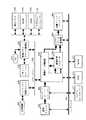
つぎに、本実施の形態にかかる画像処理装置がディジタル複合機を構成する場合のハードウエア構成について説明する。図2は本実施の形態にかかる画像処理装置のハードウエア構成の一例を示すブロック図である。
【0039】
図2のブロック図において、本実施の形態にかかる画像処理装置は、読取ユニット201と、センサー・ボード・ユニット202と、画像データ制御部203と、画像処理プロセッサー204と、ビデオ・データ制御部205と、作像ユニット(エンジン)206とを備える。また、本実施の形態にかかる画像処理装置は、シリアルバス210を介して、プロセス・コントローラー211と、RAM212と、ROM213とを備える。
【0040】
また、本実施の形態にかかる画像処理装置は、パラレルバス220を介して、画像メモリー・アクセス制御部221とファクシミリ制御ユニット224とを備え、さらに、画像メモリー・アクセス制御部221に接続されるメモリー・モジュール222と、システム・コントローラー231と、RAM232と、ROM233と、操作パネル234とを備える。
【0041】
ここで、上記各構成部と、図1に示した各ユニット100〜104との関係について説明する。すなわち、読取ユニット201およびセンサー・ボード・ユニット202により、図1に示した画像読取ユニット101の機能を実現する。また同様に、画像データ制御部203により、画像データ制御ユニット100の機能を実現する。また同様に、画像処理プロセッサー204により画像処理ユニット103の機能を実現する。
【0042】
また同様に、ビデオ・データ制御部205および作像ユニット(エンジン)206により画像書込ユニット104を実現する。また同様に、画像メモリー・アクセス制御部221およびメモリー・モジュール222により画像メモリー制御ユニット102を実現する。
【0043】
つぎに、各構成部の内容について説明する。原稿を光学的に読み取る読取ユニット201は、ランプとミラーとレンズから構成され、原稿に対するランプ照射の反射光をミラーおよびレンズにより受光素子に集光する。
【0044】
受光素子、たとえばCCDは、センサー・ボード・ユニット202に搭載され、CCDにおいて電気信号に変換された画像データはディジタル信号に変換された後、センサー・ボード・ユニット202から出力(送信)される。
【0045】
センサー・ボード・ユニット202から出力(送信)された画像データは画像データ制御部203に入力(受信)される。機能デバイス(処理ユニット)およびデータバス間における画像データの伝送は画像データ制御部203が全て制御する。
【0046】
画像データ制御部203は、画像データに関し、センサー・ボード・ユニット202、パラレルバス220、画像処理プロセッサー204間のデータ転送、画像データに対するプロセス・コントローラー211と画像処理装置の全体制御を司るシステム・コントローラー231との間の通信をおこなう。また、RAM212はプロセス・コントローラー211のワークエリアとして使用され、ROM213はプロセス・コントローラー211のブートプログラム等を記憶している。
【0047】
センサー・ボード・ユニット202から出力(送信)された画像データは画像データ制御部203を経由して画像処理プロセッサー204に転送(送信)され、光学系およびディジタル信号への量子化にともなう信号劣化(スキャナー系の信号劣化とする)を補正し、再度、画像データ制御部203へ出力(送信)される。
【0048】
画像メモリー・アクセス制御部221は、メモリー・モジュール222に対する画像データの書き込み/読み出しを制御する。また、パラレルバス220に接続される各構成部の動作を制御する。また、RAM232はシステム・コントローラー231のワークエリアとして使用され、ROM233はシステム・コントローラー231のブートプログラム等を記憶している。
【0049】
操作パネル234は、画像処理装置がおこなうべき処理を入力する。たとえば、処理の種類(複写、ファクシミリ送信、画像読込、プリント等)および処理の枚数等を入力する。これにより、画像データ制御情報の入力をおこなうことができる。なお、ファクシミリ制御ユニット224の内容については後述する。
【0050】
つぎに、読み取った画像データにはメモリー・モジュール222に蓄積して再利用するジョブと、メモリー・モジュール222に蓄積しないジョブとがあり、それぞれの場合について説明する。メモリー・モジュール222に蓄積する例としては、1枚の原稿について複数枚を複写する場合に、読取ユニット201を1回だけ動作させ、読取ユニット201により読み取った画像データをメモリー・モジュール222に蓄積し、蓄積された画像データを複数回読み出すという方法がある。
【0051】
メモリー・モジュール222を使わない例としては、1枚の原稿を1枚だけ複写する場合に、読み取り画像データをそのまま再生すればよいので、画像メモリー・アクセス制御部221によるメモリー・モジュール222へのアクセスをおこなう必要はない。
【0052】
まず、メモリー・モジュール222を使わない場合、画像処理プロセッサー204から画像データ制御部203へ転送されたデータは、再度画像データ制御部203から画像処理プロセッサー204へ戻される。画像処理プロセッサー204においては、センサー・ボード・ユニット202におけるCCDによる輝度データを面積階調に変換するための画質処理をおこなう。
【0053】
画質処理後の画像データは画像処理プロセッサー204からビデオ・データ制御部205に転送される。面積階調に変化された信号に対し、ドット配置に関する後処理およびドットを再現するためのパルス制御をおこない、その後、作像ユニット206において転写紙上に再生画像を形成する。
【0054】
つぎに、メモリー・モジュール222に蓄積し画像読み出し時に付加的な処理、たとえば画像方向の回転、画像の合成等をおこなう場合の画像データの流れについて説明する。画像処理プロセッサー204から画像データ制御部203へ転送された画像データは、画像データ制御部203からパラレルバス220を経由して画像メモリー・アクセス制御部221に送られる。
【0055】
ここでは、システム・コントローラー231の制御に基づいて画像データとメモリー・モジュール222のアクセス制御、外部PC(パーソナル・コンピューター)223のプリント用データの展開、メモリー・モジュール222の有効活用のための画像データの圧縮/伸張をおこなう。
【0056】
画像メモリー・アクセス制御部221へ送られた画像データは、データ圧縮後メモリー・モジュール222へ蓄積され、蓄積された画像データは必要に応じて読み出される。読み出された画像データは伸張され、本来の画像データに戻し画像メモリー・アクセス制御部221からパラレルバス220を経由して画像データ制御部203へ戻される。
【0057】
画像データ制御部203から画像処理プロセッサー204への転送後は画質処理、およびビデオ・データ制御部205でのパルス制御をおこない、作像ユニット206において転写紙上に再生画像を形成する。
【0058】
画像データの流れにおいて、パラレルバス220および画像データ制御部203でのバス制御により、ディジタル複合機の機能を実現する。ファクシミリ送信機能は読み取られた画像データを画像処理プロセッサー204にて画像処理を実施し、画像データ制御部203およびパラレルバス220を経由してファクシミリ制御ユニット224へ転送する。ファクシミリ制御ユニット224にて通信網へのデータ変換をおこない、公衆回線(PN)225へファクシミリデータとして送信する。
【0059】
一方、受信されたファクシミリデータは、公衆回線(PN)225からの回線データをファクシミリ制御ユニット224にて画像データへ変換され、パラレルバス220および画像データ制御部203を経由して画像処理プロセッサー204へ転送される。この場合、特別な画質処理はおこなわず、ビデオ・データ制御部205においてドット再配置およびパルス制御をおこない、作像ユニット206において転写紙上に再生画像を形成する。
【0060】
複数ジョブ、たとえば、コピー機能、ファクシミリ送受信機能、プリンター出力機能が並行に動作する状況において、読取ユニット201、作像ユニット206およびパラレルバス220の使用権のジョブへの割り振りをシステム・コントローラー231およびプロセス・コントローラー211において制御する。
【0061】
プロセス・コントローラー211は画像データの流れを制御し、システム・コントローラー231はシステム全体を制御し、各リソースの起動を管理する。また、ディジタル複合機の機能選択は操作パネル(操作部)234において選択入力し、コピー機能、ファクシミリ機能等の処理内容を設定する。
【0062】
システム・コントローラー231とプロセス・コントローラー211は、パラレルバス220、画像データ制御部203およびシリアルバス210を介して相互に通信をおこなう。具体的には、画像データ制御部203内においてパラレルバス220とシリアルバス210とのデータ・インターフェースのためのデータフォーマット変換をおこなうことにより、システム・コントローラー231とプロセス・コントローラー211間の通信をおこなう。
【0063】
(単体スキャナーのハードウエア構成)
つぎに、本実施の形態にかかる画像処理装置が単体スキャナーを構成する場合のハードウエア構成について説明する。図3は本実施の形態にかかる画像処理装置のハードウエア構成の別の一例を示すブロック図である。なお、図2に示したハードウエア構成のブロック図において、同一の構成部については同一の符号を付してその説明を省略する。
【0064】
ハードウエアのシステム構成において図3に示す単体スキャナーと図2に示したディジタル複合機と大きく異なる点は、作像ユニット206がない点である。作像ユニットが不要なのでビデオ・データ制御部205も装着されない。
【0065】
読取ユニット201において読み込まれた画像データは、センサー・ボード・ユニット202においてディジタル変換され、画像データ制御部203を介して画像処理プロセッサー204に転送された後、画像処理プロセッサー204において単体スキャナーとして要求される画像処理をおこなう。
【0066】
単体スキャナーとして要求される主な画像処理は、読み取られた画像の劣化補正であるが、画面を使った表示装置に適する階調処理もおこなうことができる。したがって、転写紙を対象とした画質処理とは異なる処理が多い。
【0067】
ここで、画像処理プロセッサー204をプログラマブルな演算処理装置により構成することで、転写紙への画質処理、画面への階調処理に関して必要な処理手順のみを設定すればよく、画質処理の手順と階調処理の手順を常に両方持ち合わせる必要はないことになる。
【0068】
階調処理後の画像データは画像データ制御部203へ転送され、パラレルバス220を経由して画像メモリー・アクセス制御部221に送信される。ここで、バッファー・メモリーとしてメモリー・モジュール222を使用し、PC223に付属するドライバーに対して画像データを転送することにより、スキャナー機能を実現する。
【0069】
ディジタル複合機と同様に、システム・コントローラー231とプロセス・コントローラー211により画像データおよびシステムのリソース管理をおこなう。
【0070】
(画像処理ユニット103/画像処理プロセッサー204)
つぎに、画像処理ユニット103を構成する画像処理プロセッサー204における処理の概要について説明する。図4は本実施の形態にかかる画像処理装置の画像処理プロセッサー204の処理の概要を示すブロック図である。
【0071】
図4のブロック図において、画像処理プロセッサー204は、第1入力I/F401と、スキャナー画像処理部402と、第1出力I/F403と、第2入力I/F404と、画質処理部405と、第2出力I/F406とを含む構成となっている。
【0072】
上記構成において、読み取られた画像データはセンサー・ボード・ユニット202、画像データ制御部203を介して画像処理プロセッサー204の第1入力インターフェース(I/F)401からスキャナー画像処理部402へ伝達される。
【0073】
スキャナー画像処理部402は読み取られた画像データの劣化を補正することを目的とし、具体的には、シェーディング補正、スキャナーγ補正、MTF補正等をおこなう。補正処理ではないが、拡大/縮小の変倍処理もおこなうことができる。読み取り画像データの補正処理が終了すると、第1出力インターフェース(I/F)403を介して画像データ制御部203へ画像データを転送する。
【0074】
転写紙への出力の際は、画像データ制御部203からの画像データを第2入力I/F404より受信し、画質処理部405において面積階調処理をおこなう。画質処理後の画像データは第2出力I/F406を介してビデオ・データ制御部205または画像データ制御部203へ出力される。
【0075】
画質処理部405における面積階調処理は、濃度変換処理、ディザ処理、誤差拡散処理等があり、階調情報の面積近似を主な処理とする。一旦、スキャナー画像処理部402により処理された画像データをメモリー・モジュール222に蓄積しておけば、画質処理部405により画質処理を変えることによって種々の再生画像を確認することができる。
【0076】
たとえば、再生画像の濃度を振って(変更して)みたり、ディザマトリクスの線数を変更してみたりすることにより、再生画像の雰囲気を容易に変更することができる。この際、処理を変更するごとに画像を読取ユニット201からの読み込みをやり直す必要はなく、メモリー・モジュール222から蓄積された画像データを読み出すことにより、同一画像データに対して、何度でも異なる処理を迅速に実施することができる。
【0077】
また、単体スキャナーの場合、スキャナー画像処理と階調処理を合せて実施し、画像データ制御部203へ出力する。処理内容はプログラマブルに変更することができる。処理の切り替え、処理手順の変更等はシリアルI/F408を介してコマンド制御部407において管理する。
【0078】
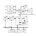
(画像データ制御ユニット100/画像データ制御部203)
つぎに、画像データ制御ユニット100を構成する画像データ制御部203における処理の概要について説明する。図5は本実施の形態にかかる画像処理装置の画像データ制御部203の処理の概要を示すブロック図である。
【0079】
図5のブロック図において、画像データ入出力制御部501は、センサー・ボード・ユニット202からの画像データを入力(受信)し、画像処理プロセッサー204に対して画像データを出力(送信)する。すなわち、画像データ入出力制御部501は、画像読取ユニット101と画像処理ユニット103(画像処理プロセッサー204)とを、接続するための構成部であり、画像読取ユニット101により読み取られた画像データを画像処理ユニット103へ送信するためだけの専用の入出力部であるといえる。
【0080】
また、画像データ入力制御部502は、画像処理プロセッサー204でスキャナー画像補正された画像データを入力(受信)する。入力された画像データはパラレルバス220における転送効率を高めるために、データ圧縮部503においてデータ圧縮処理をおこなう。その後、データ変換部504を経由し、パラレルデータI/F505を介してパラレルバス220へ送出される。
【0081】
パラレルバス220からパラレルデータI/F505を介して入力される画像データは、バス転送のために圧縮されているため、データ変換部504を経由してデータ伸張部506へ送られ、そこでデータ伸張処理をおこなう。伸張された画像データは画像データ出力制御部507において画像処理プロセッサー204へ転送される。
【0082】
また、画像データ制御部203は、パラレルデータとシリアルデータの変換機能も備えている。システム・コントローラー231はパラレルバス220にデータを転送し、プロセス・コントローラー211はシリアルバス210にデータを転送する。画像データ制御部203は2つのコントローラーの通信のためにデータ変換をおこなう。
【0083】
また、シリアルデータI/Fは、シリアルバス210を介してプロセス・コントローラーとのデータのやりとりをする第1シリアルデータI/F508と、画像処理プロセッサー204とのデータのやりとりに用いる第2シリアルデータI/F509を備える。画像処理プロセッサー204との間に独立に1系統持つことにより、画像処理プロセッサー204とのインターフェースを円滑化することができる。
【0084】
コマンド制御部510は、入力された命令にしたがって、上述した画像データ制御部203内の各構成部および各インターフェースの動作を制御する。なお、コマンド制御部510等による画像データの送受信の制御については、後で詳述する。
【0085】
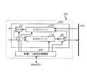
つぎに、画像データ制御部203の内部構成について説明する。図6は、画像データ制御部203の内部構成を示すブロック図である。ここでは、画像データ制御部203に入力した画像データを画像処理プロセッサー204に送信する場合について説明するが、他の機能ユニットと接続する場合についても同様な画像データの送受信制御がおこなわれる。
【0086】
図6において、画像データ送受信制御部601は、画像データの送受信を制御する。具体的には、画像データ送受信制御部601は、画像データの出力経路を切り替える切替部602や、パラレルバス220およびシリアルバス210と画像データおよび制御信号を入出力するバスI/F603等を制御する。また、ラインバッファー604は、パラレルバス220等に画像データを送信する際に送信タイミングなどを調整する際に使用される。
【0087】
なお、図6において、画像データ送受信制御部601は、図5におけるコマンド制御部510および画像データ入出力制御部501、画像データ入力制御部502、画像データ出力制御部507を機能的に示したものであり、また、バスI/F603は、図5における第1シリアルデータI/F508、第2シリアルデータI/F509およびパラレルデータI/F505を機能的に示したものである。
【0088】
つぎに、画像データ送受信制御部601と、切替部602の動作について説明する。図7は、画像データ制御部203における画像データの処理の流れを示すフローチャートである。
【0089】
画像データ制御部203は、画像処理プロセッサー204における稼働情報を入力する(ステップS701)。この稼働情報は、画像処理プロセッサー204の動作タイミングや動作クロック、もしくは、他の画像データの処理待ちの有無に関する情報などから構成され、画像処理プロセッサー204に画像データの入力があった場合に、当該画像データを直ちに滞りなく処理可能であるか否かを判断する際の判断情報である。稼働情報は、画像処理プロセッサー204の稼働状況やシステム・コントローラー231の制御状況をもとに作成される。
【0090】
画像データ送受信制御部601は、稼働情報をもとに、画像データ制御部203内の画像データを、出力先である画像処理プロセッサー204に送信可能であるか否かを判断する(ステップS702)。
【0091】
画像処理プロセッサー204が画像データを処理可能である場合は(ステップS702肯定)、画像データ送受信制御部601は、切替部602を制御して、当該画像データをそのまま直接画像処理プロセッサー204に送出する(ステップS703)。すなわち、この場合は、パラレルバス220を介することなく画像データを画像処理プロセッサー204に直接送出する。
【0092】
一方、稼働情報から、画像処理プロセッサー204が画像データを直ちに処理できず、処理が開始できるまでには時間がかかると判断した場合は(ステップS702否定)、画像データ送受信制御部601は、バスI/F603を制御して、画像メモリー・アクセス制御部221に画像データを送出し、画像メモリー・アクセス制御部221の制御の下、当該画像データをメモリー・モジュール222に格納する(ステップS704)。
【0093】
すなわち、ステップS704では、パラレルバス220を介して画像データをメモリー・モジュール222に一旦格納する。メモリー・モジュール222では、複数の機能ユニットとの間で、様々な画像データが頻繁に入出力される。したがって、各画像データは秩序だてて送受信される必要があり、このため、パラレルバス220およびラインバッファー604が必要となる。
【0094】
その後、画像処理プロセッサー204で画像データの処理が可能となったか否かが判断され(ステップS705)、処理可能であれば(ステップS705肯定)、メモリー・モジュール222に格納された画像データは、パラレルバス220を介して画像処理プロセッサー204に送出される(ステップS706)。
【0095】
一般的に、各機能ユニットごとに作り分けされたディジタル複合機は、バスを介して相互に接続することとなり、バスの制御が重要となる。特にメモリーの重複を避けて、メモリー・モジュール222で一括して画像データを保存する場合においては、使用率が非常に高くなる。上述のような切替制御により、入力した画像データ全てを一旦画像メモリー・アクセス制御部221に格納する必要はなくなる。
【0096】
すなわち、送信先の機能ユニットに送信可能な場合は、ラインバッファー604やパラレルバス220を介さず直接送信するので、これにより、バスの使用頻度を低減させ、画像処理装置全体として効率的な画像データの送受信をおこなうことが可能となる。
【0097】
(画像書込ユニット104/ビデオ・データ制御部205)
つぎに、画像書込ユニット104の一部を構成するビデオ・データ制御部205における処理の概要について説明する。図8は本実施の形態にかかる画像処理装置のビデオ・データ制御部205の処理の概要を示すブロック図である。
【0098】
図8のブロック図において、ビデオ・データ制御部205は、入力される画像データに対して、作像ユニット206の特性に応じて、追加の処理をおこなう。すなわち、エッジ平滑処理部801がエッジ平滑処理によるドットの再配置処理をおこない、パルス制御部802がドット形成のための画像信号のパルス制御をおこない、上記の処理がおこなわれた画像データを作像ユニット206へ出力する。
【0099】
ビデオ・データ制御部205は、画像データの変換とは別に、パラレルデータとシリアルデータのフォーマット変換機能を備え、ビデオ・データ制御部205単体でもシステム・コントローラー231とプロセス・コントローラー211の通信に対応することができる。すなわち、パラレルデータを送受信するパラレルデータI/F803と、シリアルデータを送受信するシリアルデータI/F804と、パラレルデータI/F803およびシリアルデータI/F804により受信されたデータを相互に変換するデータ変換部805とを備えることにより、両データのフォーマットを変換する。
【0100】
(画像メモリー制御ユニット102/画像メモリー・アクセス制御部221)
つぎに、画像メモリー制御ユニット102の一部を構成する画像メモリー・アクセス制御部221における処理の概要について説明する。図9は本実施の形態にかかる画像処理装置の画像メモリー・アクセス制御部221の処理の概要を示すブロック図である。
【0101】
図9のブロック図において、画像メモリー・アクセス制御部221は、パラレルバス220との画像データのインターフェースを管理し、また、メモリー・モジュール222への画像データのアクセス、すなわち格納(書込み)/読出しを制御し、また、主に外部のPC223から入力されるコードデータの画像データへの展開を制御する。
【0102】
そのために、画像メモリー・アクセス制御部221は、パラレルデータI/F901と、システム・コントローラーI/F902と、メモリー・アクセス制御部903と、ラインバッファー904と、ビデオ制御部905と、データ圧縮部906と、データ伸張部907と、データ変換部908と、を含む構成である。
【0103】
ここで、パラレルデータI/F901は、パラレルバス220との画像データのインターフェースを管理する。また、メモリー・アクセス制御部903は、メモリー・モジュール222への画像データのアクセス、すなわち格納(書込み)/読出しを制御する。
【0104】
また、入力されたコードデータは、ラインバッファー904において、ローカル領域でのデータの格納をおこなう。ラインバッファー904に格納されたコードデータは、システム・コントローラーI/F902を介して入力されたシステム・コントローラー231からの展開処理命令に基づき、ビデオ制御部905において画像データに展開される。
【0105】
展開された画像データもしくはパラレルデータI/F901を介してパラレルバス220から入力された画像データは、メモリー・モジュール222に格納される。この場合、データ変換部908において格納対象となる画像データを選択し、データ圧縮部906においてメモリー使用効率を上げるためにデータ圧縮をおこない、メモリー・アクセス制御部903にてメモリー・モジュール222のアドレスを管理しながらメモリー・モジュール222に画像データを格納(書込)する。
【0106】
メモリー・モジュール222に格納(蓄積)された画像データの読み出しは、メモリー・アクセス制御部903において読み出し先アドレスを制御し、読み出された画像データをデータ伸張部907において伸張する。伸張された画像データをパラレルバス220へ転送する場合、パラレルデータI/F901を介してデータ転送をおこなう。
【0107】
(ファクシミリ制御ユニット224の構成)
つぎに、ファクシミリ制御ユニット224の機能的な構成について説明する。図10は、本実施の形態における画像処理装置のファクシミリ制御ユニット224の構成を示すブロック図である。
【0108】
図10のブロック図において、ファクシミリ制御ユニット224は、ファクシミリ送受信部1001と外部I/F1002とから構成される。ここで、ファクシミリ送受信部1001は、画像データを通信形式に変換して外部回線に送信し、また、外部からのデータを画像データに戻して外部I/F1002およびパラレルバス220を介して作像ユニットにおいて記録出力する。
【0109】
ファクシミリ送受信部1001は、ファクシミリ画像処理部1003、画像メモリー1004、メモリー制御部1005、データ制御部1006、画像圧縮伸張部1007、モデム1008および網制御装置1009を含む構成である。
【0110】
このうち、ファクシミリ画像処理に関し、受信画像に対する二値スムージング処理は、図8に示したビデオ・データ制御部205内のエッジ平滑処理部801においておこなう。また、画像メモリー1004に関しても、出力バッファー機能に関しては画像メモリー・アクセス制御部221およびメモリー・モジュール222にその機能の一部を移行する。
【0111】
このように構成されたファクシミリ送受信部1001では、画像データの伝送を開始するとき、データ制御部1006がメモリー制御部1005に指令し、画像メモリー1004から蓄積している画像データを順次読み出させる。読み出された画像データは、ファクシミリ画像処理部1003によって元の信号に復元されるとともに、密度変換処理および変倍処理がなされ、データ制御部1006に加えられる。
【0112】
データ制御部1006に加えられた画像データは、画像圧縮伸張部1007によって符号圧縮され、モデム1008によって変調された後、網制御装置1009を介して宛先へと送出される。そして、送信が完了した画像情報は、画像メモリー1004から削除される。
【0113】
受信時には、受信画像は一旦画像メモリー1004に蓄積され、そのときに受信画像を記録出力可能であれば、1枚分の画像の受信を完了した時点で記録出力する。また、複写動作時に発呼されて受信を開始したときは、画像メモリー1004の使用率が所定値、たとえば80%に達するまでは画像メモリー1004に蓄積し、画像メモリー1004の使用率が80%に達した場合には、そのときに実行している書き込み動作を強制的に中断し、受信画像を画像メモリー1004から読み出し記録出力する。
【0114】
このとき画像メモリー1004から読み出した受信画像は画像メモリー1004から削除し、画像メモリー1004の使用率が所定値、たとえば10%まで低下した時点で中断していた書き込み動作を再開し、その書き込み動作を全て終了した時点で、残りの受信画像を記録出力する。また、書き込み動作を中断した後に、再開できるように中断時における書き込み動作のための各種パラメーターを内部的に退避し、再開時に、パラメーターを内部的に復帰する。
【0115】
実施の形態1の画像処理装置は、画像データ制御部203が、他の機能ユニットに画像データを送信する際に、パラレルバス220を介さずに直接当該機能ユニットに画像データを送信するか、パラレルバス220を介して画像データをメモリー・モジュール222に一時保管しておき、後に当該機能ユニットに画像データを送信するかを切り替えるので、バスの混雑を低減し、これにより、多機能を実現する際のシステムにおける各資源の有効活用を図り、システム全体として最適な画像データの送受信の制御が可能となる。
【0116】
また、画像読取ユニットおよび/または画像データ制御ユニットおよび/または画像メモリー制御ユニットおよび/または画像処理ユニットおよび/または画像書込ユニットおよび/またはファクシミリ制御ユニットをそれぞれ独立のユニットとして構成するので、MFP、単体スキャナー、単体プリンター等、データ処理系が似ている機器の作り分けを容易におこなうことができ、各資源の重複を低減し、低コストで多機能なシステムを構築できる。
【0117】
〔実施の形態2〕
実施の形態2では、画像データ制御部203内で、入力した画像データを一時保持し、バスの混雑を低減する画像処理装置について説明する。なお、実施の形態2では、実施の形態1に示した構成と同一の部分については同一の符合を付してその説明を省略する。
【0118】
図11は、実施の形態2における画像処理装置の画像データ制御部の内部構成を示すブロック図である。本実施の形態における画像処理装置は、画像データ制御部203内のバスI/F603(図6参照)に、画像データの入力用の入力ラインバッファー1101と、画像データの出力用の出力ラインバッファー1102とを備える。
【0119】
入力ラインバッファー1101および出力ラインバッファー1102はパラレルバス220における秩序だったデータの入出力を確保するために設けられるものである。ここでラインバッファーの動作について説明する。一般的に、画像データ制御部203からパラレルバス220経由で出力される画像データは、出力ラインバッファー1102への書き込みが終わることにより出力が可能となる。このとき、出力ラインバッファー1102への書き込みが終了したときにフラグを立て(制御信号を発し)、画像データをパラレルバス220への転送可能となった旨を知らせる。
【0120】
反対に、パラレルバス220から入力してくる画像データも、入力ラインバッファー1101への書き込みが終了したときにフラグを立て、画像データ制御部203内に画像データを転送可能となった旨を知らせる。
【0121】
バスI/F603は、さらに、入力ラインバッファー1101の出力先にスイッチS1を、出力ラインバッファー1102の出力先にスイッチS2を備え、それぞれ入力ラインバッファー1101から出力される画像データを出力ラインバッファー1102に入力させ、出力ラインバッファー1102から出力される画像データを入力ラインバッファー1101に入力させることができる構成となっている。
【0122】
画像データ送受信制御部601は、前述したフラグをもとに、スイッチS1およびスイッチS2の切替制御をおこなって、出力ラインバッファー1102に格納された画像データを、可能な限り入力ラインバッファー1101と出力ラインバッファー1102との間で入出力させる。これにより、いわば時間稼ぎをおこなって、画像データを画像処理プロセッサー204に送信可能となるまで、画像データ制御部203内に保持することが可能となる。
【0123】
画像データ送受信制御部601の切替制御により、画像データをパラレルバス220に送出せずにすむので、バスの使用頻度を低減させ、画像処理装置全体として効率的な画像データの送受信をおこなうことが可能となる。なお、操作パネル234(図2参照)を介して、画像データを画像データ制御部203内に保持する態様であってもよい。
【0124】
また、スイッチS1およびスイッチS2の制御タイミングや、画像データの処理の優先度を変更して、画像処理装置全体としてもっとも効率的な画像データの送受信制御をおこなわせることもできる。これは、操作パネル234を介して新たな制御アルゴリズム(プログラム)をRAM232に格納することにより実現できる。すなわち、プログラムを変更することにより、システム仕様変更、機能追加に容易に対応することができる。
【0125】
【発明の効果】
以上説明したように、この発明によれば、画像データ制御ユニットが、画像データを読み取る画像読取ユニットおよび/または画像データに対し加工編集等の画像処理を施す画像処理ユニットおよび/または画像データを転写紙等に書き込む画像書込ユニット、および、画像メモリーを制御して画像データの書込み/読出しをおこなう画像メモリー制御ユニットに接続し、判断手段が前記画像データ制御ユニットから画像データを送信する送信先ユニットにおいて当該画像データを処理できるか否かを判断し、第1の送信手段が画像データを前記画像データ制御ユニットから前記送信先ユニットへ直接送信し、第2の送信手段が画像データを前記画像データ制御ユニットから前記画像メモリー制御ユニットへ順序付けをおこなって送信し、切替手段が前記第1の送信手段と第2の送信手段とを切り替え、前記画像データ制御ユニットに備わり当該画像データ制御ユニットに接続された各ユニットの間で画像データの送受信の制御をおこなう送受信制御手段が、前記切替手段を制御して、前記判断手段により画像データが処理可能であると判断された場合には前記第1の送信手段に当該画像データを送信し、前記判断手段により画像データが処理不可能であると判断された場合には前記第2の送信手段に当該画像データを送信するので、画像データの処理待ちが必要な場合は当該画像データを画像メモリーへ送信し、処理待ちが必要でない場合は当該画像データを送信先の機能ユニットに直接送信することができ、これにより、多機能を実現する際のシステムにおける各資源の有効活用を図り、システム全体として最適な画像データの送受信の制御が可能な画像処理装置が得られるという効果を奏する。
【0126】
また、この発明によれば、上記発明において、前記画像データ制御ユニットが、受信バッファーと送信バッファーとを備え、受信バッファーが当該画像データ制御ユニットにより受信される画像データを一時格納し、送信バッファーが当該画像データ制御ユニットにより送信される画像データを一時格納し、前記送受信制御手段が、前記送信バッファーおよび受信バッファーを制御して、前記送信バッファーから出力される画像データを前記受信バッファーに入力し、前記受信バッファーから出力される当該画像データを前記送信バッファーに入力するので、処理待ちが必要な画像データを画像メモリーに送信することなく、画像データ制御部で保持することができ、これにより、多機能を実現する際のシステムにおける各資源の有効活用を図り、システム全体として最適な画像データの送受信の制御が可能な画像処理装置が得られるという効果を奏する。
【0127】
また、この発明によれば、上記発明において、記録手段が前記送受信制御手段の制御内容を記録し、書換手段が前記記録手段を書き換えるので、画像処理装置の装置規模に応じて画像データの転送制御の内容を変更することができ、これにより、多機能を実現する際のシステムにおける各資源の有効活用を図り、システム全体として最適な画像データの送受信の制御が可能な画像処理装置が得られるという効果を奏する。
【図面の簡単な説明】
【図1】 この発明の本実施の形態にかかる画像処理装置の構成を機能的に示すブロック図である。
【図2】 実施の形態1にかかる画像処理装置のハードウエア構成の一例を示すブロック図である。
【図3】 実施の形態1にかかる画像処理装置のハードウエア構成の別の一例を示すブロック図である。
【図4】 実施の形態1にかかる画像処理装置の画像処理プロセッサーの処理の概要を示すブロック図である。
【図5】 実施の形態1にかかる画像処理装置の画像データ制御部の処理の概要を示すブロック図である。
【図6】 実施の形態1にかかる画像処理装置の画像データ制御部の内部構成を示すブロック図である。
【図7】 実施の形態1にかかる画像処理装置の画像データ制御部における画像データの処理の流れを示すフローチャートである。
【図8】 実施の形態1にかかる画像処理装置のビデオ・データ制御部の処理の概要を示すブロック図である。
【図9】 実施の形態1にかかる画像処理装置の画像メモリー・アクセス制御部の処理の概要を示すブロック図である。
【図10】 実施の形態1における画像処理装置のファクシミリ制御ユニットの構成を示すブロック図である。
【図11】 実施の形態2における画像処理装置の画像データ制御部の内部構成を示すブロック図である。
【図12】 従来技術にかかるディジタル複合機のハードウエア構成を示すブロック図である。
【符号の説明】
100 画像データ制御ユニット
101 画像読取ユニット
102 画像メモリー制御ユニット
103 画像処理ユニット
104 画像書込ユニット
201 読取ユニット
202 センサー・ボード・ユニット
203 画像データ制御部
204 画像処理プロセッサー
205 ビデオ・データ制御部
206 作像ユニット
210 シリアルバス
211 プロセス・コントローラー
220 パラレルバス
221 画像メモリー・アクセス制御部
222 メモリー・モジュール
224 ファクシミリ制御ユニット
231 システム・コントローラー
234 操作パネル
408 シリアルI/F
501 画像データ入出力制御部
502 画像データ入力制御部
503 データ圧縮部
504 データ変換部
505 パラレルデータI/F
506 データ伸張部
507 画像データ出力制御部
508 第1シリアルデータI/F
509 第2シリアルデータI/F
510 コマンド制御部
601 画像データ送受信制御部
602 切替部
603 バスI/F
604 ラインバッファー
803 パラレルデータI/F
804 シリアルデータI/F
901 パラレルデータI/F
902 システム・コントローラーI/F
903 メモリー・アクセス制御部
904 ラインバッファー
905 ビデオ制御部
906 データ圧縮部
907 データ伸張部
908 データ変換部
1001 ファクシミリ送受信部
1003 ファクシミリ画像処理部
1004 画像メモリー
1005 メモリー制御部
1006 データ制御部
1101 入力ラインバッファー
1102 出力ラインバッファー
S1、S2 スイッチ[0001]
BACKGROUND OF THE INVENTION
The present invention relates to an image processing apparatus that performs image processing on digital image data, and in particular, performs image processing on image data in a digital multi-function peripheral that combines functions of a copying machine, a facsimile, a printer, a scanner, and the like.
[0002]
[Prior art]
Conventionally, digital copiers that process image data digitized from analog copiers have appeared. Furthermore, digital copiers not only function as copiers, but also function of facsimile, There are digital multifunction peripherals that combine functions such as printer functions and scanner functions.
[0003]
FIG. 12 is a block diagram showing a hardware configuration of a digital multifunction peripheral according to the prior art. As shown in FIG. 12, the digital multi-function peripheral is formed by a series of components of a
[0004]
Therefore, the copying machine part that realizes the function as a copying machine is configured by the
[0005]
In other words, the functions of the digital multi-function peripheral are realized by adding on the
[0006]
Also disclosed is an “image processing apparatus” (for example, Japanese Patent Laid-Open No. 8-274986) that optimizes image processing of read signals, image storage in a memory, parallel operation of a plurality of functions, and respective image processing. Some image processing can be executed with a single image processing configuration.
[0007]
[Problems to be solved by the invention]
However, in the above-described digital multi-function peripheral, since the copying machine portion is established as one system as described above, the copying machine portion such as the
[0008]
Therefore, the memory modules necessary for realizing the function of each control unit must be configured so that each unit has each. Therefore, each unit cannot effectively utilize the
[0009]
Similarly, since the copier portion is established as one system, there is a problem that the function improvement accompanying the performance improvement of the peripheral unit cannot be efficiently achieved. When it is desired to change only the
[0010]
That is, since a series of systems has already been established so that the entire copying machine portion can be read / written at 400 dpi, when converting the above units, the matrix size for intermediate processing is reduced. It is necessary to change the threshold value. Also, the setting contents of other units may need to be changed so that reading / writing can be performed at 600 dpi.
[0011]
Therefore, when it is configured by hardware such as ASIC, the hardware (customized IC, LSI, etc.) itself must be replaced. Therefore, as the performance of the peripheral unit is improved, the function of the entire apparatus cannot be easily improved by simply replacing the peripheral unit.
[0012]
In addition, with respect to a conventional digital multifunction peripheral in which each functional unit is added on via the
[0013]
That is, in order to transmit and receive image data between the functional units, it is necessary to provide a bus (image data bus) that is commonly used among the units. Here, in each functional unit, when the device starts operation, it is often impossible to stop transmission / reception of image data. Particularly in the case of a unit configuration in which a memory module for storing image data is separately provided for the purpose of effective use of memory resources, it becomes impossible to stop transmission / reception of image data in each unit.
[0014]
Therefore, when constructing a bus used for transmission / reception of image data, the bus speed and bus width are determined from the maximum simultaneous operation of a plurality of devices, which is assumed in advance, so that the image processing apparatus as a whole can efficiently process image data. It is necessary to send and receive. However, when a digital multifunction peripheral is modularized for each function, the upgrade of each functional module may exceed the initially assumed maximum simultaneous operation, and image data may not be transmitted or received successfully. There was a problem that there was.
[0015]
Furthermore, since the parts constituting the copying machine are established as one system, there is a problem that the function division cannot be easily performed when the digital multifunction peripheral is used as a single scanner or single printer.
[0016]
As described above, the conventional digital multifunction peripherals are optimally controlled in terms of effective use of each resource in the system, such as sharing modules, improving functions by replacing each unit, and dividing multiple functions. There was a problem that the configuration was not built.
[0017]
In order to solve the above-described problems caused by the prior art, the present invention aims to effectively utilize each resource in a system for realizing a multi-function, and can control transmission / reception of optimal image data as a whole system. The purpose is to provide.
[0018]
[Means for Solving the Problems]
In order to solve the above-described problems and achieve the object, an image processing apparatus according to the present invention includes an image reading unit that reads image data and / or an image processing unit that performs image processing such as processing and editing on image data, and / or Connects to an image writing unit that writes image data on transfer paper, etc., and an image memory control unit that controls image memory to write / read image data, and send / receive image data to / from each connected unit In the image processing apparatus provided with the image data control unit having the transmission / reception control means for performing the above control, the determination means for determining whether or not the image data can be processed in the transmission destination unit that transmits the image data from the image data control unit Image data from the image data control unit to the destination unit First transmission means for direct transmission, second transmission means for ordering and transmitting image data from the image data control unit to the image memory control unit, the first transmission means and the second transmission means Switching means for switching between, and when the transmission / reception control means controls the switching means and the determination means determines that the image data can be processed, the transmission means controls the first transmission means. The image data is transmitted, and when the determination unit determines that the image data cannot be processed, the image data is transmitted to the second transmission unit.
[0019]
According to the present invention, when waiting for processing of image data is required, the image data can be transmitted to the image memory, and when waiting for processing is not required, the image data can be directly transmitted to the functional unit of the transmission destination.
[0020]
In the image processing apparatus according to the present invention as set forth in the invention described above, the image data control unit is transmitted by the image data control unit and a reception buffer that temporarily stores image data received by the image data control unit. A transmission buffer for temporarily storing image data, wherein the transmission / reception control unit controls the transmission buffer and the reception buffer, and inputs the image data output from the transmission buffer to the reception buffer; The image data output from is input to the transmission buffer.
[0021]
According to the present invention, the image data that needs to be processed can be held in the image data control unit without being transmitted to the image memory.
[0022]
The image processing apparatus according to the present invention is characterized in that, in the above invention, the image processing apparatus comprises recording means for recording the control contents of the transmission / reception control means and rewriting means for rewriting the recording means.
[0023]
According to the present invention, the content of image data transfer control can be changed according to the scale of the image processing apparatus.
[0024]
DETAILED DESCRIPTION OF THE INVENTION
Exemplary embodiments of an image processing apparatus according to the present invention will be explained below in detail with reference to the accompanying drawings.
[0025]
[Embodiment 1]
First, the principle of the image processing apparatus according to this embodiment will be described. FIG. 1 is a block diagram functionally showing the configuration of the image processing apparatus according to this embodiment of the present invention. In FIG. 1, the image processing apparatus includes the following five units.
[0026]
The five units are an image
[0027]
Each of the above units has an
[0028]
(Image data control unit 100)
The processes performed by the image
[0029]
For example,
(1) Data compression processing (primary compression) for improving data bus transfer efficiency,
(2) Transfer processing of primary compressed data to image data,
(3) Image composition processing (image data from a plurality of units can be composed. In addition, composition on a data bus is also included),
(4) Image shift processing (image shift in the main scanning and sub-scanning directions),
(5) Image area expansion processing (it is possible to enlarge the image area to the periphery by an arbitrary amount),
(6) Image scaling processing (for example, 50% or 200% fixed scaling),
(7) Parallel bus interface processing,
(8) Serial bus interface processing (interface with
(9) Parallel data and serial data format conversion processing,
(10) Interface processing with the
(11) Interface processing with the
Etc.
[0030]
(Image reading unit 101)
The processes performed by the
[0031]
For example,
(1) Document reflected light reading process by optical system,
(2) Conversion processing into an electric signal in a CCD (Charge Coupled Device).
(3) Digitization processing by A / D converter,
(4) Shading correction processing (processing for correcting illuminance distribution unevenness of the light source),
(5) Scanner γ correction processing (processing for correcting the density characteristics of the reading system),
Etc.
[0032]
(Image memory control unit 102)
The processing performed by the image
[0033]
For example,
(1) Interface control processing with the system controller,
(2) Parallel bus control processing (interface control processing with parallel bus),
(3) Network control processing,
(4) Serial bus control processing (control processing of multiple external serial ports),
(5) Internal bus interface control processing (command control processing with the operation unit),
(6) Local bus control processing (ROM, RAM, font data access control processing for starting the system controller),
(7) Memory module operation control processing (memory module write / read control processing, etc.)
(8) Memory module access control processing (processing to arbitrate memory access requests from multiple units),
(9) Data compression / decompression processing (processing to reduce the amount of data for effective use of memory),
(10) Image editing processing (memory area data clear, image data rotation processing, image composition processing in memory, etc.),
Etc.
[0034]
(Image processing unit 103)
The processing performed by the
[0035]
For example,
(1) Shading correction processing (processing for correcting illuminance distribution unevenness of the light source),
(2) Scanner γ correction processing (processing for correcting the density characteristics of the reading process),
(3) MTF correction processing,
(4) Smoothing process
(5) Arbitrary scaling processing in the main scanning direction,
(6) Density conversion (γ conversion processing: corresponding to density notch),
(7) Simple multi-value processing
(8) Simple binarization processing,
(9) error diffusion processing,
(10) Dither processing,
(11) Dot arrangement phase control processing (right dot, left dot),
(12) Isolated point removal processing,
(13) Image area separation processing (color determination, attribute determination, adaptive processing),
(14) Density conversion processing,
Etc.
[0036]
(Image writing unit 104)
The processes performed by the
[0037]
For example,
(1) Edge smoothing process (jaggy correction process),
(2) Correction processing for dot rearrangement,
(3) Image signal pulse control processing,
(4) Parallel data and serial data format conversion processing,
Etc.
[0038]
(Hardware configuration of digital multifunction device)
Next, a hardware configuration when the image processing apparatus according to the present embodiment constitutes a digital multi-function peripheral will be described. FIG. 2 is a block diagram showing an example of a hardware configuration of the image processing apparatus according to the present embodiment.
[0039]
In the block diagram of FIG. 2, the image processing apparatus according to the present embodiment includes a
[0040]
Further, the image processing apparatus according to the present embodiment includes an image memory /
[0041]
Here, the relationship between each component described above and each
[0042]
Similarly, the
[0043]
Next, the contents of each component will be described. A
[0044]
A light receiving element, for example, a CCD is mounted on the
[0045]
Image data output (transmitted) from the
[0046]
The image
[0047]
The image data output (transmitted) from the
[0048]
The image memory
[0049]
The
[0050]
Next, the read image data includes a job that is stored in the
[0051]
As an example of not using the
[0052]
First, when the
[0053]
The image data after the image quality processing is transferred from the
[0054]
Next, a description will be given of the flow of image data in the case where additional processing such as rotation of the image direction, image synthesis, and the like is performed at the time of image reading stored in the
[0055]
Here, based on the control of the
[0056]
The image data sent to the image memory
[0057]
After transfer from the image
[0058]
In the flow of image data, the functions of the digital multifunction peripheral are realized by the bus control in the
[0059]
On the other hand, the received facsimile data is converted from the line data from the public line (PN) 225 to image data by the
[0060]
In a situation where a plurality of jobs, for example, a copy function, a facsimile transmission / reception function, and a printer output function operate in parallel, the
[0061]
The
[0062]
The
[0063]
(Hardware configuration of a single scanner)
Next, a hardware configuration when the image processing apparatus according to the present embodiment forms a single scanner will be described. FIG. 3 is a block diagram showing another example of the hardware configuration of the image processing apparatus according to the present embodiment. In the block diagram of the hardware configuration shown in FIG. 2, the same components are denoted by the same reference numerals, and description thereof is omitted.
[0064]
The hardware system configuration differs greatly from the single scanner shown in FIG. 3 and the digital multifunction machine shown in FIG. 2 in that there is no
[0065]
The image data read by the
[0066]
The main image processing required as a single scanner is correction of deterioration of a read image, but gradation processing suitable for a display device using a screen can also be performed. Therefore, there are many processes different from the image quality process for transfer paper.
[0067]
Here, by configuring the
[0068]
The image data after gradation processing is transferred to the image
[0069]
As with the digital multi-function peripheral, image data and system resources are managed by the
[0070]
(
Next, an outline of processing in the
[0071]
In the block diagram of FIG. 4, the
[0072]
In the above configuration, the read image data is transmitted from the first input interface (I / F) 401 of the
[0073]
The scanner
[0074]
When outputting to the transfer sheet, the image data from the image
[0075]
Area gradation processing in the image
[0076]
For example, the atmosphere of the reproduced image can be easily changed by changing (changing) the density of the reproduced image or by changing the number of lines of the dither matrix. At this time, it is not necessary to read the image again from the
[0077]
In the case of a single scanner, scanner image processing and gradation processing are performed together and output to the image
[0078]
(Image
Next, an outline of processing in the image
[0079]
In the block diagram of FIG. 5, the image data input /
[0080]
The image data
[0081]
Since the image data input from the
[0082]
The image
[0083]
The serial data I / F includes a first serial data I /
[0084]
The command control unit 510 controls the operation of each component unit and each interface in the image
[0085]
Next, the internal configuration of the image
[0086]
In FIG. 6, an image data transmission /
[0087]
In FIG. 6, the image data transmission /
[0088]
Next, operations of the image data transmission /
[0089]
The image
[0090]
Based on the operation information, the image data transmission /
[0091]
If the
[0092]
On the other hand, when it is determined from the operation information that the
[0093]
That is, in step S 704, the image data is temporarily stored in the
[0094]
Thereafter, it is determined whether the
[0095]
In general, digital multifunction peripherals created for each functional unit are connected to each other via a bus, and control of the bus is important. In particular, in the case where image data is collectively stored in the
[0096]
That is, when transmission to the functional unit of the transmission destination is possible, the transmission is performed directly without using the
[0097]
(
Next, an outline of processing in the video /
[0098]
In the block diagram of FIG. 8, the video
[0099]
The video
[0100]
(Image
Next, an outline of processing in the image memory /
[0101]
In the block diagram of FIG. 9, the image memory
[0102]
For this purpose, the image memory
[0103]
Here, the parallel data I /
[0104]
The input code data is stored in the local area in the
[0105]
The expanded image data or the image data input from the
[0106]
When reading out the image data stored (accumulated) in the
[0107]
(Configuration of facsimile control unit 224)
Next, a functional configuration of the
[0108]
In the block diagram of FIG. 10, the
[0109]
The facsimile transmission /
[0110]
Among them, regarding the facsimile image processing, the binary smoothing processing for the received image is performed in the edge smoothing
[0111]
In the facsimile transmission /
[0112]
Image data added to the
[0113]
At the time of reception, the received image is temporarily stored in the
[0114]
At this time, the received image read from the
[0115]
In the image processing apparatus according to the first embodiment, when the image
[0116]
Further, since the image reading unit and / or the image data control unit and / or the image memory control unit and / or the image processing unit and / or the image writing unit and / or the facsimile control unit are configured as independent units, the MFP, Devices with similar data processing systems, such as single scanners and single printers, can be easily created, reducing the duplication of resources and building a multifunctional system at low cost.
[0117]
[Embodiment 2]
In the second embodiment, an image processing apparatus that temporarily stores input image data and reduces bus congestion in the image
[0118]
FIG. 11 is a block diagram illustrating an internal configuration of the image data control unit of the image processing apparatus according to the second embodiment. The image processing apparatus according to the present embodiment has an
[0119]
The
[0120]
On the other hand, the image data input from the
[0121]
The bus I /
[0122]
The image data transmission /
[0123]
By switching control of the image data transmission /
[0124]
Further, the control timing of the switch S1 and the switch S2 and the priority of image data processing can be changed to perform the most efficient image data transmission / reception control as the entire image processing apparatus. This can be realized by storing a new control algorithm (program) in the
[0125]
【The invention's effect】
As described above, according to the present invention, the image data control unit transfers the image reading unit that reads the image data and / or the image processing unit that performs image processing such as processing editing on the image data and / or the image data. An image writing unit for writing on paper or the like, and an image memory control unit for controlling the image memory to write / read image data, and a destination unit for transmitting the image data from the image data control unit The first transmission unit directly transmits the image data from the image data control unit to the transmission destination unit, and the second transmission unit transmits the image data to the image data. The control unit performs ordering and transmission to the image memory control unit. Transmission / reception control means for controlling transmission / reception of image data between the units connected to the image data control unit provided in the image data control unit by switching means between the first transmission means and the second transmission means However, when the switching means is controlled and the determination means determines that the image data can be processed, the image data is transmitted to the first transmission means, and the image data is processed by the determination means. If it is determined that the image data is impossible, the image data is transmitted to the second transmission means. Therefore, if it is necessary to wait for the processing of the image data, the image data is transmitted to the image memory and the processing needs to be waited for. If not, the image data can be directly transmitted to the functional unit of the transmission destination, which makes it possible to effectively use each resource in the system when realizing multiple functions. The aim, an effect that the control is capable of image processing apparatus of the transmission and reception of the optimum image data in the entire system is obtained.
[0126]
According to the invention, in the above invention, the image data control unit includes a reception buffer and a transmission buffer. The reception buffer temporarily stores image data received by the image data control unit. Temporarily storing the image data transmitted by the image data control unit, the transmission / reception control unit controls the transmission buffer and the reception buffer, and inputs the image data output from the transmission buffer to the reception buffer, Since the image data output from the reception buffer is input to the transmission buffer, the image data that needs to be processed can be held in the image data control unit without being transmitted to the image memory. Effective use of each resource in the system when realizing the function Ri is an effect that the control is capable of image processing apparatus of the transmission and reception of the optimum image data in the entire system is obtained.
[0127]
According to this invention, in the above invention, the recording means records the control contents of the transmission / reception control means, and the rewriting means rewrites the recording means. Therefore, transfer control of image data according to the device scale of the image processing apparatus. It is possible to change the contents of the image processing device, thereby effectively using each resource in the system when realizing a multi-function, and obtaining an image processing apparatus capable of controlling transmission / reception of optimal image data as a whole system. There is an effect.
[Brief description of the drawings]
FIG. 1 is a block diagram functionally showing the configuration of an image processing apparatus according to an embodiment of the present invention.
FIG. 2 is a block diagram illustrating an example of a hardware configuration of the image processing apparatus according to the first embodiment.
FIG. 3 is a block diagram illustrating another example of the hardware configuration of the image processing apparatus according to the first embodiment;
FIG. 4 is a block diagram showing an outline of processing of an image processing processor of the image processing apparatus according to the first embodiment;
FIG. 5 is a block diagram illustrating an outline of processing of an image data control unit of the image processing apparatus according to the first embodiment;
FIG. 6 is a block diagram showing an internal configuration of an image data control unit of the image processing apparatus according to the first embodiment;
FIG. 7 is a flowchart showing a flow of processing of image data in an image data control unit of the image processing apparatus according to the first embodiment;
FIG. 8 is a block diagram illustrating an outline of processing of a video data control unit of the image processing apparatus according to the first embodiment;
FIG. 9 is a block diagram showing an outline of processing of an image memory / access control unit of the image processing apparatus according to the first embodiment;
10 is a block diagram showing a configuration of a facsimile control unit of the image processing apparatus according to
11 is a block diagram illustrating an internal configuration of an image data control unit of an image processing apparatus according to Embodiment 2. FIG.
FIG. 12 is a block diagram showing a hardware configuration of a digital multifunction peripheral according to a conventional technique.
[Explanation of symbols]
100 Image data control unit
101 Image reading unit
102 Image memory control unit
103 Image processing unit
104 Image writing unit
201 Reading unit
202 Sensor board unit
203 Image data control unit
204 Image processor
205 Video data controller
206 Imaging unit
210 Serial bus
211 Process controller
220 Parallel bus
221 Image memory access controller
222 Memory module
224 Facsimile control unit
231 System Controller
234 Operation panel
408 Serial I / F
501 Image data input / output control unit
502 Image data input control unit
503 Data compression unit
504 Data converter
505 Parallel data I / F
506 Data decompression unit
507 Image data output control unit
508 First serial data I / F
509 Second serial data I / F
510 Command control unit
601 Image data transmission / reception control unit
602 switching unit
603 Bus I / F
604 line buffer
803 Parallel data I / F
804 Serial data I / F
901 Parallel data I / F
902 System controller I / F
903 Memory access control unit
904 line buffer
905 Video control unit
906 Data compression unit
907 Data decompression unit
908 Data converter
1001 Facsimile transceiver
1003 Facsimile image processing unit
1004 Image memory
1005 Memory control unit
1006 Data control unit
1101 Input line buffer
1102 Output line buffer
S1, S2 switch
Claims (6)
Translated fromJapanese前記制御手段は、
前記処理手段または前記記憶手段に送信する画像データを格納するための送信データ格納手段と、
前記送信データ格納手段との間で画像データの出入力が可能であり、前記処理手段または前記記憶手段から受信した画像データを格納するための受信データ格納手段と、
前記送信データ格納手段から前記処理手段に画像データを送信した場合、前記処理手段において、前記送信された画像データに対する処理が実行可能な期間であるか否かを判断する判断手段と、
を備え、
前記制御手段は、前記判断手段により前記画像データに対する処理が実行不可能な期間と判断された場合、前記画像データを前記送信データ格納手段と前記受信データ格納手段との間で画像データの出入力をさせることを特徴とする画像処理装置。One or more processing means for performing predetermined processing on the image data, storage means for storing the image data processed by the processing means, connected to the processing means and the storage means, the processing means and the Control means for controlling transmission / reception of image data to / from storage means,
The control means includes
Transmission data storage means for storing image data to be transmitted to the processing means or the storage means;
Received data storage means for storing image data received from the processing means or the storage means, capable of inputting / outputting image data to / from the transmission data storage means;
A determination unit that determines whether or not it is a period in which processing for the transmitted image data can be performed in the processing unit when the image data is transmitted from the transmission data storage unit to the processing unit;
With
The control means outputs and inputs the image data between the transmission data storage means and the reception data storage means when the determination means determines that the process for the image data cannot be performed. An image processing apparatus characterized in that
前記判断手段は、前記稼動情報作成手段により作成された稼動情報に基づいて、前記画像データに対する処理が実行不可能な期間であるか否かの判断をおこなうことを特徴とする請求項1または2に記載の画像処理装置。Furthermore, an operation information creation unit indicating an operation status of the processing unit is provided,
3. The determination unit according to claim 1, wherein the determination unit determines whether or not it is a period during which processing for the image data cannot be performed, based on the operation information created by the operation information creation unit. An image processing apparatus according to 1.
前記制御手段は、前記優先度に基づいて、データの送信先を切り替えることを特徴とする請求項1〜5のいずれか一つに記載の画像処理装置。In place of the determination means, a priority determination means for determining the priority of processing by the processing means,
The image processing apparatus according to claim 1, wherein the control unit switches a data transmission destination based on the priority.
Priority Applications (1)
| Application Number | Priority Date | Filing Date | Title |
|---|---|---|---|
| JP35989099AJP3670918B2 (en) | 1999-12-17 | 1999-12-17 | Image processing device |
Applications Claiming Priority (1)
| Application Number | Priority Date | Filing Date | Title |
|---|---|---|---|
| JP35989099AJP3670918B2 (en) | 1999-12-17 | 1999-12-17 | Image processing device |
Publications (2)
| Publication Number | Publication Date |
|---|---|
| JP2001177682A JP2001177682A (en) | 2001-06-29 |
| JP3670918B2true JP3670918B2 (en) | 2005-07-13 |
Family
ID=18466824
Family Applications (1)
| Application Number | Title | Priority Date | Filing Date |
|---|---|---|---|
| JP35989099AExpired - Fee RelatedJP3670918B2 (en) | 1999-12-17 | 1999-12-17 | Image processing device |
Country Status (1)
| Country | Link |
|---|---|
| JP (1) | JP3670918B2 (en) |
Cited By (1)
| Publication number | Priority date | Publication date | Assignee | Title |
|---|---|---|---|---|
| JP2008017231A (en)* | 2006-07-06 | 2008-01-24 | Ricoh Co Ltd | Communication device |
- 1999
- 1999-12-17JPJP35989099Apatent/JP3670918B2/ennot_activeExpired - Fee Related
Cited By (1)
| Publication number | Priority date | Publication date | Assignee | Title |
|---|---|---|---|---|
| JP2008017231A (en)* | 2006-07-06 | 2008-01-24 | Ricoh Co Ltd | Communication device |
Also Published As
| Publication number | Publication date |
|---|---|
| JP2001177682A (en) | 2001-06-29 |
Similar Documents
| Publication | Publication Date | Title |
|---|---|---|
| JP3660182B2 (en) | Image processing device | |
| JP3789711B2 (en) | Image processing device | |
| JP3732702B2 (en) | Image processing device | |
| US7673165B2 (en) | Image processing device, method for saving power consumption of the image processing device, and a computer product | |
| US20010054126A1 (en) | SIMD type processor, method and apparatus for parallel processing, devices that use the SIMD type processor or the parallel processing apparatus, method and apparatus for image processing, computer product | |
| JP3974730B2 (en) | Image processing apparatus, image processing procedure in image processing apparatus, method for adding and updating data for image processing, and computer-readable recording medium recording program for causing computer to execute the method | |
| US6930793B1 (en) | Image processing apparatus, image processing method and computer readable recording medium for recording program for computer to execute the method | |
| JP3657156B2 (en) | Image processing device | |
| JP4378197B2 (en) | Image information device | |
| JP2001144920A (en) | IMAGE PROCESSING DEVICE, IMAGE PROCESSING METHOD, AND COMPUTER-READABLE RECORDING MEDIUM RECORDING PROGRAM FOR CAUSING COMPUTER TO EXECUTE THE METHOD | |
| JP3670918B2 (en) | Image processing device | |
| JP2001126057A (en) | Image processing device | |
| JP3825796B2 (en) | Image processing device | |
| JP4063840B2 (en) | Image processing device | |
| JP2018118477A (en) | Image processing device, control method and program of the same | |
| JP2001186355A (en) | Image processing device | |
| JP2004112692A (en) | Image processing device | |
| JP3785295B2 (en) | Image processing device | |
| JP2004343624A (en) | Image processing apparatus, image forming apparatus, image processing method, computer program, and recording medium | |
| JP3730070B2 (en) | Image processing apparatus, image processing method, and computer-readable recording medium storing program for causing computer to execute the method | |
| JP2005323406A (en) | Image processing apparatus, image processing method, program for causing computer to execute the method, and computer-readable recording medium storing the program | |
| JP2002042124A (en) | Image processing device | |
| JP2004179692A (en) | Image processing apparatus, image processing method, and program for causing computer to execute this method | |
| JP2004048113A (en) | Image processing device | |
| JP2001177721A (en) | IMAGE PROCESSING DEVICE, IMAGE PROCESSING METHOD, AND COMPUTER-READABLE RECORDING MEDIUM RECORDING PROGRAM FOR CAUSING COMPUTER TO EXECUTE THE METHOD |
Legal Events
| Date | Code | Title | Description |
|---|---|---|---|
| A977 | Report on retrieval | Free format text:JAPANESE INTERMEDIATE CODE: A971007 Effective date:20041208 | |
| A131 | Notification of reasons for refusal | Free format text:JAPANESE INTERMEDIATE CODE: A131 Effective date:20041214 | |
| A521 | Written amendment | Free format text:JAPANESE INTERMEDIATE CODE: A523 Effective date:20050209 | |
| TRDD | Decision of grant or rejection written | ||
| A01 | Written decision to grant a patent or to grant a registration (utility model) | Free format text:JAPANESE INTERMEDIATE CODE: A01 Effective date:20050412 | |
| A61 | First payment of annual fees (during grant procedure) | Free format text:JAPANESE INTERMEDIATE CODE: A61 Effective date:20050415 | |
| R150 | Certificate of patent or registration of utility model | Free format text:JAPANESE INTERMEDIATE CODE: R150 | |
| FPAY | Renewal fee payment (event date is renewal date of database) | Free format text:PAYMENT UNTIL: 20080422 Year of fee payment:3 | |
| FPAY | Renewal fee payment (event date is renewal date of database) | Free format text:PAYMENT UNTIL: 20090422 Year of fee payment:4 | |
| FPAY | Renewal fee payment (event date is renewal date of database) | Free format text:PAYMENT UNTIL: 20100422 Year of fee payment:5 | |
| FPAY | Renewal fee payment (event date is renewal date of database) | Free format text:PAYMENT UNTIL: 20100422 Year of fee payment:5 | |
| FPAY | Renewal fee payment (event date is renewal date of database) | Free format text:PAYMENT UNTIL: 20110422 Year of fee payment:6 | |
| FPAY | Renewal fee payment (event date is renewal date of database) | Free format text:PAYMENT UNTIL: 20120422 Year of fee payment:7 | |
| FPAY | Renewal fee payment (event date is renewal date of database) | Free format text:PAYMENT UNTIL: 20130422 Year of fee payment:8 | |
| FPAY | Renewal fee payment (event date is renewal date of database) | Free format text:PAYMENT UNTIL: 20140422 Year of fee payment:9 | |
| LAPS | Cancellation because of no payment of annual fees |