JP3669836B2 - IDDQ test cycle selective extraction device - Google Patents
IDDQ test cycle selective extraction deviceDownload PDFInfo
- Publication number
- JP3669836B2 JP3669836B2JP07025498AJP7025498AJP3669836B2JP 3669836 B2JP3669836 B2JP 3669836B2JP 07025498 AJP07025498 AJP 07025498AJP 7025498 AJP7025498 AJP 7025498AJP 3669836 B2JP3669836 B2JP 3669836B2
- Authority
- JP
- Japan
- Prior art keywords
- bit data
- cycle
- data
- bit
- test
- Prior art date
- Legal status (The legal status is an assumption and is not a legal conclusion. Google has not performed a legal analysis and makes no representation as to the accuracy of the status listed.)
- Expired - Fee Related
Links
Images


Classifications
- G—PHYSICS
- G01—MEASURING; TESTING
- G01R—MEASURING ELECTRIC VARIABLES; MEASURING MAGNETIC VARIABLES
- G01R31/00—Arrangements for testing electric properties; Arrangements for locating electric faults; Arrangements for electrical testing characterised by what is being tested not provided for elsewhere
- G01R31/28—Testing of electronic circuits, e.g. by signal tracer
- G01R31/30—Marginal testing, e.g. by varying supply voltage
- G01R31/3004—Current or voltage test
- G01R31/3008—Quiescent current [IDDQ] test or leakage current test
- G—PHYSICS
- G01—MEASURING; TESTING
- G01R—MEASURING ELECTRIC VARIABLES; MEASURING MAGNETIC VARIABLES
- G01R31/00—Arrangements for testing electric properties; Arrangements for locating electric faults; Arrangements for electrical testing characterised by what is being tested not provided for elsewhere
- G01R31/28—Testing of electronic circuits, e.g. by signal tracer
- G01R31/317—Testing of digital circuits
- G01R31/3181—Functional testing
- G01R31/3183—Generation of test inputs, e.g. test vectors, patterns or sequences
- G01R31/318342—Generation of test inputs, e.g. test vectors, patterns or sequences by preliminary fault modelling, e.g. analysis, simulation
Landscapes
- Engineering & Computer Science (AREA)
- General Engineering & Computer Science (AREA)
- Physics & Mathematics (AREA)
- General Physics & Mathematics (AREA)
- Tests Of Electronic Circuits (AREA)
Description
Translated fromJapanese【0001】
【発明の属する技術分野】
本発明は、論理シミュレーションを利用して、半導体集積回路のIDDQテスト用のサイクルを選択抽出する装置及び選択抽出の方法に関する。
【0002】
【従来の技術】
CMOS集積回路の微細化、高集積化が進むにつれて、テスト工程の負担が急激に増加している。実際、テストパターンの数は年々増加している。厄介なことに、現在主流のファンクションテストでは発見しにくいタイプの新たな故障が増加する傾向にある。この新たな故障は、例えば、開放故障やスイッチング動作時の過渡状態でしか発生しない故障等である。
このため、上記ファンクションテストのみを実施した場合、上記新たな故障を含んでいるものが良品として出荷されてしまい、機器に組み込まれてしまうケースが増加しつつある。
【0003】
上記のファンクションテストでは検出できない新たな故障を検出するための新たなテスト方法としてIDDQテストが着目されている。IDDQテストは、スタンバイ状態にあるCMOS集積回路に流れる微少な電源電流を測定し、その電流値の大小によって故障を検出するものである。これは、正常なCMOS回路では、そのスタンバイ状態において、電源電流は僅かしか流れないことを利用するものである。即ち、スタンバイ状態においてCMOS回路に多量の電流が流れる場合には、回路内に何らかの欠陥(故障)を含んでいることを意味する。通常の集積回路の動作時、その内部状態は時々刻々変化するが、動作中の各サイクルの内、スタンバイ状態を実現しているサイクルを検出し、検出したサイクルにおけるスタンバイ電流を測定することでIDDQテストを実行することができる。
【0004】
ところで、論理シミュレーションを使って、あるサイクルにおいてスタンバイ状態が実現されているかどうかを知る技術については周知である。例えば、特開平4−44172号公報では、以下の4つの条件が満たされている時が電源電流を測定するべきスタンバイ状態であるとしている。
(1)複数のゲートの出力信号が競合する(バスコンフリクトの)状態でないこと。
(2)バスに接続されている全てのゲート出力がハイインピーダンス”Z”の状態ではないこと。
(3)プルアップ付きのノードの論理値が”H”であること。
(4)プルダウン付きのノードの論理値が”L”であること。
【0005】
【発明が解決しようとする課題】
テストの品質(=そのテストによる故障検出能力)だけを考慮するならば、できるだけ多様な内部状態でのテストを行った方がよい。従って、スタンバイ状態が実現されている全てのサイクルについてテストを行うことが最も望ましい。しかし、実際には、テスト時間がそのまま製造コストに影響してくるため、テストの品質を一定のレベルに維持しつつ、できるだけテスト時間を短くすることが要求される。
【0006】
また、IDDQテストは、電流を測定するものである。一般に電流測定は電圧測定よりも時間がかかるため、テスト時間を短くするには、電流の測定回数を減らすことが望まれる。それには、全スタンバイサイクルでテストするのではなく、テストの品質を維持するのに必要にして十分なスタンバイサイクルを選択抽出することが要求される。
【0007】
既に述べたように、実際に製造された半導体集積回路に対して、その機能動作をテストするいわゆるファンクションテストは必ず実施される。ところが、このファンクションテストでは、検出される故障の一部は、当該ファンクションテストを補うために実施するIDDQテストにおいても検出される場合がある。
【0008】
しかし、従来のテスト装置は、このことについて何等考慮しておらず、IDDQテストにおいては、全ての故障をターゲットとしてテストサイクル(若しくはテストパターン)を選択・抽出する。このため、以下のような問題が生じる。
【0009】
第1に半導体集積回路のテスト時間が不必要に長くなる。これは、そのまま半導体集積回路のコストアップにつながる。
第2にIDDQテスト装置が1つの半導体集積回路に占有される時間が不必要に長くなる。これは半導体集積回路の開発期間、開発効率を悪化させ、結果的に半導体集積回路のコストアップにつながる。
【0010】
本発明は、上記従来の装置の有する課題を解決すべくなされたものであり、ファンクションテストで検出されない故障のみをターゲットとする必要にして十分な数のIDDQテスト用サイクルを迅速に選択・抽出する装置を提供することを目的とする。
【0011】
【課題を解決するための手段】
本発明の請求項1記載のIDDQテスト用サイクル選択抽出装置は、CMOS集積回路の論理シミュレーション中に現れたn個のスタンバイ状態のサイクルにおける各m個のネットの状態を表すmビットデータの中から、mビットデータを構成する全てのビットの値が少なくとも1回は“1”及び“0”となる組み合わせとなるmビットデータの組み合わせを、IDDQテスト用のサイクルとして選択抽出するIDDQテスト用サイクル選択抽出装置であって、n個のスタンバイ状態のサイクルにおけるmビットデータを保存するデータ保存手段と、所定のテストパターンを用いて実行したCMOS集積回路の故障シミュレーションの結果に基づいて、テストパターンにより故障が検出されたネットを特定する故障シミュレーション手段と、n個のスタンバイ状態のサイクルにおける各mビットデータの内、故障シミュレーション手段により特定される、故障が検出されたネットに対応する位置のビットデータを、IDDQテスト用サイクル選択抽出の処理対象外とする制御手段とを備えることを特徴とする。
【0012】
本発明の請求項2記載のIDDQテスト用サイクル選択抽出装置は、上記請求項1記載のIDDQテスト用サイクル選択抽出装置において、更に、mビットデータを構成する各ビットに一対一に対応する、m個のトグル済みフラグを記憶する記憶手段と、mビットデータが順次与えられ、与えられたmビットデータに基づいてトグル済みフラグを更新する更新手段であって、新たに与えられたmビットデータと、その前に与えられたmビットデータとに関し、未だトグル済みフラグのセットされていない位置のビットデータ同士の比較を行い、一方が“1”で他方が“0”のデータ値を持つビットデータについてはトグル済みフラグをセットするフラグ更新手段と、データ保存手段に記憶するn個のmビットデータの内、トグル済みフラグのセットされていない位置のビットデータ同士に着目し、互いのハミング距離の最も遠い2つのmビットデータを選択し、選択した2つのmビットデータを、第1及び第2のIDDQテスト用のサイクルのmビットデータとして、順にフラグ更新手段に与える第1データ選択手段と、フラグ更新手段によるトグル済みフラグの更新後、mビットデータの内、未だトグル済みフラグがセットされていないビットデータの位置を認識する認識手段と、認識手段により未だトグル済みフラグがセットされていないと認識された位置のビットデータだけに着目して、既に選択抽出されたIDDQテスト用のサイクルのmビットデータとのハミング距離が最も遠く、かつ、未だ選択されていないIDDQテスト用のサイクルのmビットデータを、データ保存手段に保存されているmビットデータ内から選択し、選択したmビットデータを、新たなIDDQテスト用のサイクルのmビットデータとして、フラグ更新手段に与える第2データ選択手段とを備え、制御手段は、第1データ選択手段が2つのmビットデータを選択する前に、故障シミュレーション手段により故障が検出されたネットに対応するビット位置のトグル済みフラグをセットしてIDDQテスト用サイクル選択抽出の処理対象外とすることを特徴とする。
【0013】
請求項3記載のIDDQテスト用サイクル選択抽出装置は、請求項1記載のIDDQテスト用サイクル選択抽出装置において、更に、CMOS集積回路の論理シミュレーションを実行する論理シミュレーション手段と、論理シミュレーション手段によるシミュレーション実行時における動作サイクル毎に、当該サイクルに前記集積回路がスタンバイ状態にあるか否かを判断する判断手段と、判断手段により最初にスタンバイ状態であると判断されたサイクルを第1のIDDQテスト用サイクルとして選択する第1サイクル選択手段と、mビットのデータを構成する各ビットに一対一に対応するトグル済みフラグの記憶手段と、第1サイクル選択手段による選択の後に、判断手段によりスタンバイ状態にあると判断されるサイクルの中から、上記選択された第1のIDDQテスト用のサイクルにおける上記CMOS集積回路内のm個のネットの状態を表すmビットのデータの内、トグル済みフラグのセットされていないビットの位置のみに着目した場合に、ハミング距離が上記着目するビットの数に応じて決まるしきい値よりも大きなmビットのデータを有する最初のサイクルを、第2のIDDQテスト用のサイクルとして選択する第2サイクル選択手段と、第1及び第2サイクル選択手段により第1及び第2のIDDQテスト用として選択された2つのサイクルにおける回路内のm個のネットの状態を表す2つのmビットデータを保存するデータ保存手段と、mビットデータが順次与えられ、与えられたmビットデータに基づいて、トグル済みフラグを更新する更新手段であって、新たに与えられたmビットデータ及びその前に与えられたmビットデータのトグル済みフラグのセットされていないビットのデータについて、ビット単位の比較を行い、一方が“1”で他方が“0”のデータ値を持つビットに対応するトグル済みフラグをセットするフラグ更新手段と、データ保存手段に保存する2つのmビットデータを第1及び第2の選択抽出データとして選択し、順にフラグ更新手段に与える第1データ選択手段と、フラグ更新手段によるトグル済みフラグの更新後、未だトグル済みフラグがセットされていないビットデータの位置を認識する認識手段と、既に選択したmビットデータの内、認識手段により未だトグル済みフラグがセットされていないと認識されたビット位置のみに着目し、判断手段によりスタンバイ状態であると判断されたサイクルであって、上記着目するビット位置でのハミング距離が上記しきい値よりも大きいmビットデータを示すサイクルを選択し、選択したサイクルのmビットデータを、フラグ更新手段に与える第2データ選択手段とを備え、制御手段は、第1データ選択手段による選択の前に、故障シミュレーション手段により故障が検出されたネットに対応するビット位置のトグル済みフラグをセットしてIDDQテスト用サイクル選択抽出の処理対象外とすることを特徴とする。
【0014】
請求項4記載のIDDQテスト用サイクル選択抽出装置は、請求項2又は請求項3に記載のIDDQテスト用サイクル選択抽出装置において、第2データ選択手段は、トグル認識レジスタ内におけるトグル済みフラグが立ったビットの個数が所定値以上になった場合に、新たな選択抽出データとして選択したmビットデータの上記フラグ更新手段への出力を停止することを特徴とする。
【0015】
請求項5記載のIDDQテスト用サイクル選択抽出装置は、請求項2又は請求項3に記載のIDDQテスト用サイクル抽出装置において、第2データ選択手段は、予め決めた数のIDDQテスト用のサイクルが選択抽出された場合に、新たな選択抽出データとして選択したmビットデータの上記フラグ更新手段への出力を停止することを特徴とする。
【0016】
なお、上記課題を解決するため、コンピュータを請求項1記載のIDDQテスト用サイクル選択抽出装置として機能させるプログラム、を記録した記録媒体を提供してもよい。
【0017】
【発明の実施の形態】
本発明のIDDQテスト用サイクルの選択装置は、ファンクションテストでは検出できない故障のみをターゲットとしてIDDQテストを実行することを特徴とする。
以下、上記特徴を具備するIDDQテスト用サイクル選択抽出装置の実施の形態について、添付の図面を用いて説明する。
【0018】
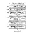
(1)実施の形態1
(1-1)機能ブロック
図1は、実施の形態1にかかるIDDQテスト用サイクル選択抽出装置150のブロック構成図である。
外部装置として設けられている論理シミュレーション装置100は、所定のハードウェア記述言語を用いて記述されたCMOS集積回路の論理シミュレーションを実行し、論理シミュレーションの結果より得られるスタンバイサイクルについての情報、及び、当該論理回路の内部ネットに関する情報をIDDQテスト用サイクル選択抽出装置150へと出力する。
【0019】
また、同様に外部装置として設けられている故障シミュレーション装置110は、所定のテストパターンを用いて故障シミュレーションを実行し、どこのネットにおいてどのような故障(”0”縮退故障又は”1”縮退故障)が検出されるのか、又は、どのネットではどのような故障を検出できないのかといった情報を未検出故障データ格納部157に出力する。なお、所定のテストパターンを用いて実行した故障シミュレーションの結果に基づいて特定される故障は、同じテストパターンを用いて行うファンクションテストにより検出される故障と同じである。
【0020】
IDDQテスト用サイクル選択抽出装置150内部において、データ編集部151は、論理シミュレーション装置100より送られてくる論理シミュレーションの結果、及び、スタンバイサイクルについての情報から、回路内に全部でM個ある内部ネットの内、IDDQテスト用サイクルの選択抽出処理の対象として取り扱うm個の内部ネットを特定し、特定した各ネットの信号状態を表すmビットデータを出力する。論理シミュレーション中にスタンバイサイクルがn回現れる場合、上記mビットデータはn個出力される。
【0021】
ここで、データ編集部151では上記M個全ての内部ネットを、IDDQテスト用サイクルの選択抽出処理の対象として取り扱うこととしてもよいし、インバータやバッファ等、入力と出力が一対一に対応している素子については、その入出力ネットの何れか一方だけを、IDDQテスト用サイクルの選択抽出処理の対象として取り扱うこととしてもよい。
【0022】
また、IDDQテスト用サイクルの選択抽出処理の対象として取り扱う内部ネットは、操作者の設定に基づいて直接指定してもよいし、所定の規則に基づき区画される単位(機能ブロック、階層構造、電源系統)で指定してもよい。論理回路内に存在するM個の内部ネットは、論理シミュレーション装置100内部に備える当該論理回路の記述データに基づいて特定することができる。なお、データ編集部151は、論理シミュレーション装置100内部に設けられていてもよい。
【0023】
mビットデータ格納部152は、データ編集部151より出力されるmビットのデータを格納する。
【0024】
処理終了条件入力部153は、IDDQテスト用サイクル選択抽出部154において実行するIDDQテスト用サイクルの選択抽出条件、及び、処理終了条件を外部より設定するためのマン・マシンインターフェースである。
【0025】
未検出故障認識及びトグル認識レジスタ設定部156は、未検出故障データ格納部157に格納されている各ネットにおける故障についての情報に基づいて、トグル認識レジスタの設定を行う。後に詳しく説明するが、このトグル認識レジスタは、上記データ編集部151で処理対象として取り扱うとしたm個の内部ネットの状態を表すmビットデータの各ビットが”1”及び”0”となったか否かを示すトグル済みフラグ及び未だ”1”及び”0”となっていないデータの値を記憶しておくものである。未検出故障認識及びトグル認識レジスタ設定部156は、未検出故障データ格納部157に格納されているデータに基づいてファンクションテストで故障の検出できるネットの対応するビットのトグル済みフラグを予め”1”にセットする。
【0026】
mビットデータ格納部152には、テスト対象の回路におけるm個のネットの状態を表すmビットデータが、スタンバイサイクルの個数(n個)分格納されている。これらn個のmビットデータの中から、mビットデータを構成する各ビットの値が少なくとも1回は”1”及び”0”となる最小の組み合わせを選択抽出する。なお、上記選択抽出処理を行う際、上記データ編集部151において特定したm個のネットの内、後に実行するファンクションテストで故障の検出されるネットをテストサイクル選択抽出処理の対象外とする。このように同一のネットに対して2重に故障検出が行われるのを排除してIDDQテストに要する時間を短縮する。
【0027】
印刷・表示部155は、上記IDDQテスト用サイクル選択抽出部154により選択抽出された各サイクルについて、論理シミュレーションの開始より何番目のサイクルであるのかを表す情報を印刷または表示する。
【0028】
(1-2)ハードウェア構成
図2は、IDDQテスト用サイクルの選択抽出装置150のハードウェア構成を示す図である。本装置150は、キーボード200、マウス201、記憶装置202、データ処理装置203、ディスプレイ204、及び、プリンタ205より構成される。
【0029】
キーボード200及びマウス201は、図1に示した処理終了条件入力部153として機能する。
記憶装置202は、図1に示したmビットデータ格納部152及び未検出故障データ格納部157として機能する。
データ処理装置203は、中央演算処理装置(CPU)、及び、IDDQテスト用サイクル選択抽出処理プログラムや必要なデータを格納するメモリより構成される。データ処理装置203を構成する中央演算処理部は、IDDQテスト用サイクル選択抽出処理プログラムを実行することにより、図1に示したデータ編集部151、IDDQテスト用サイクルの選択抽出部154、及び、未検出故障認識及びトグル認識レジスタ設定部156として機能する。
ディスプレイ204及びプリンタ205は、図1に示した印刷・表示部155として機能する。
【0030】
(1-3)IDDQテスト用サイクルの選択抽出処理
図3は、データ処理装置203の実行するIDDQテスト用サイクルの選択抽出処理のフローチャートである。以下、このフローチャートを参照しつつIDDQテスト用サイクルの選択抽出処理について説明する。
【0031】
まず、論理シミュレーション装置100より送られてくる処理対象のCMOS集積回路の内部ネットについての情報に基づいて、IDDQテスト用サイクルの選択抽出処理の対象として取り扱うm個のネットを特定する(ステップS1)。ここで、上記M個全ての内部ネットを、IDDQテスト用サイクルの選択抽出処理の対象として取り扱うこととしてもよいし、インバータやバッファ等、入力と出力が一対一に対応している素子については、その入出力ネットの何れか一方だけを、IDDQテスト用サイクルの選択抽出処理の対象として取り扱うこととしてもよい。また、IDDQテスト用サイクルの選択抽出処理の対象として取り扱う内部ネットは、操作者の設定に基づいて直接指定してもよいし、所定の規則に基づき区画される単位(機能ブロック、階層構造、電源系統)で指定してもよい。
【0032】
処理対象のCMOS集積回路に対する論理シミュレーションの結果より、上記ステップS1において特定されたm個の内部ネットについて、動作サイクル(その数は回路の規模などにより変動する)中に存在したn個のスタンバイ状態の全サイクルを検出し、検出したサイクルにおける各ネットの論理値を所定の順序で並べてmビットのデータとした後に、記憶装置202に保存する(ステップS2)。
【0033】
なお、上記n個のmビットのデータは、論理シミュレーションの開始から何番目の動作サイクルであるのかを特定するデータと共に、以下の処理の便宜のため、出現タイミングの早いものから順に第1〜第nの識別番号を付して記憶装置202に保存しておく。
なお、ある動作サイクルにおいてスタンバイ状態が実現されているか否かを判断する技術については、周知であるため(例えば、特開平4−44172号公報)、ここでの説明は省略する。
【0034】
次に、トグル認識レジスタの設定を行う(ステップS3)。トグル認識レジスタは、図4に示すように各々mビット(最大でMビットである)のトグル済みフラグ記憶部250と未トグルデータ記憶部251を並べてなる合計で2×mビットのレジスタであり、データ処理装置203内に備えるメモリを用いて実現される。上記トグル済みフラグ記憶部250に記憶するトグル済みフラグは、ビットデータが”0”及び”1”の値をとり、トグル済みであると判断された場合に”1”にセットされるフラグである。また、上記未トグルデータ記憶部251は、トグルが未だ済んでいないビット位置のデータ値を記憶する。
上記ステップS3では、後に実行するファンクションテストにより検出される故障がIDDQテストの対象外になるように、トグル済みフラグ記憶部250及び未トグルデータ記憶部251の各値を設定する。例えば、所定のテストパターンを用いて行った故障シミュレーションの結果より”0”縮退故障及び”1”縮退故障の両方の故障が検出されたネットについて、対応するトグル済みフラグの値を”1”にセットする。
なお、当該処理の内容については、後に詳しく説明する。
【0035】
既に選択したmビットデータの内、トグル認識レジスタ内のトグル済みフラグ記憶部250に記憶されているフラグの値が”0”であって、かつ、未トグルデータ記憶部251に記憶されているデータの値が”0”又は”1”のデータ(以下、未トグルデータという)に着目する。
この未トグルデータと、未だ選択抽出されていない複数の各mビットデータの中から上記未トグルデータに対応するビット位置のデータを並べて構成されるデータについて、ハミング距離の最も大きなmビットデータを選択抽出する(ステップS4)。
【0036】
上記ステップS4における処理の内容について補足説明する。例えば、上記トグル認識レジスタの設定(ステップS3)において設定されたトグル済みフラグ記憶部250の内容が”1111…000”であり、未トグルデータ記憶部251の内容が”XXXX…001”(但し、Xは未確定なデータを表す)である場合を想定する。なお、該当するビットが未確定データXであるといった情報は、データ処理装置203内に備えるメモリに記録しておく。
ここで、説明の便宜のため、”…”の部分のデータについては全てトグル済みフラグが”1”であると仮定すると、未トグルデータは3ビットのデータ”001”となる。
上記ステップS4においては、上記未トグルデータ”001”について、同じく対応するビット位置のデータを並べて構成される3ビットのデータとのハミング距離が最も大きくなるmビットデータを、未だ選択抽出されていない複数のmビットデータの中から選択抽出する。例えば、”△△△△…110”(但し、△は任意のデータ)のようなmビットデータが存在する場合には、このmビットデータを選択抽出する。
【0037】
上記ステップS4において選択抽出したmビットデータとの比較を行い、上記残りのビットに関してトグル認識レジスタ内のトグル済みフラグ記憶部250の対応するビットのフラグの値を更新する(ステップS5)。なお、この更新時に未確定データXであったビットの値を、ステップS4において選択抽出したmビットデータの該当するビットの値とする。トグル認識レジスタ内のトグル済みフラグ記憶部250に記憶するトグル済みフラグの内、未だ1にセットされていないビットが存在するか、n個のmビットデータの内、未だ選択抽出されていないmビットデータが存在する場合であって(ステップS6でYES)、更に操作者により指定された処理終了条件が満足されていない場合には(ステップS7でNO)、ステップS4に戻り処理を継続する。
【0038】
他方、トグル認識レジスタ内のトグル済みフラグ250に記憶するトグル済みフラグの全ての値が1にセットされている場合、又は、n個あるmビットデータの全てが選択抽出された場合(ステップS6でNO)、処理を終了して、処理結果の出力処理を実行するステップS8へと進む。
また、上記ステップS6でYESの場合であっても、キーボード100又はマウス101の入力部を介して操作者により指定された所定の処理終了条件が満足された場合には(ステップS7でYES)、処理結果の出力を実行するステップS8へと進む。ステップS8では、選択抽出したサイクルを全てIDDQテスト用サイクルとして、これらのサイクルが論理シミュレーションの開始から何番目の動作サイクルであるのかを特定する情報(データ)をディスプレイ104に表示出力すると共に、プリンタ105により印刷出力を行う。
【0039】
(1-4)トグル認識レジスタの設定処理
図5は、トグル認識レジスタの設定処理(図3、ステップS3)のフローチャートである。また図6は、トグル認識レジスタの設定の一例について示す図である。以下、図6を参照しつつ当該処理内容についてフローに従って説明する。
【0040】
まず、トグル認識レジスタの初期化を行う(ステップS31)。この初期化では、トグル済みフラグ記憶部250及び未トグルデータ記憶部251の各mビットデータの全てを未確定データXに設定する(図6の(a)を参照)。なお、データ処理装置203に備えるメモリには、各ビット毎に未確定データXであるか否かの情報を記憶しておく。
【0041】
次に、所定のテストパターンを用いて実行した故障シミュレーションの結果を未検出故障データ格納部157より読み出す(ステップS32)。上記読み出したデータより、”0”縮退故障(stuck-at-0 fault)及び”1”縮退故障(stuck-at-1 fault)の両方が検出されているネットについては、IDDQテストで再度故障検出を行う必要がないため、トグル済みフラグの値を”1”にセットする(ステップS33)。例えば、図6の(a)に示す状態において、mビットデータの上位第1及び第2ビットがこれに該当する場合、トグル済みフラグ記憶部250の中のこれらに対応するビットの値を”1”にセットする(図6の(b)を参照)。なお、上記未トグルデータ記憶部251の第1及び第2ビットの値については未確定Xのままとする。
【0042】
上記ステップS32において読み出したデータより、”0”縮退故障及び”1”縮退故障の何れも検出されていないネットについては、該ネットを”0”及び”1”にした状態でのIDDQテストを行う必要があるため、対応する未トグルデータの値を未確定データXにした状態で、対応するビットのトグル済みフラグの値を”0”にセットする(ステップS34)。例えば、図6の(b)に示す状態において、mビットデータの上位第3及び第4ビットがこれに該当する場合、これらのビットのトグル済みフラグの値を”0”にセットする(図6の(c)を参照)。
【0043】
上記ステップS32において読み出したデータより、”0”縮退故障のみが検出されるネットについては、”1”縮退故障を検出するために該ネットを”0”にセットした状態でのIDDQテストが必要であり、対応するビットのデータの値を”1”にセットすると共に、対応するビットのトグル済みフラグの値を”0”にセットする(ステップS35)。例えば、図6の(c)に示す状態において、mビットデータの下位第3ビット目のデータがこれに該当する場合において、これらのビットのデータを”1”にセットすると共に、トグル済みフラグの値”0”にセットする(図6の(d)を参照)。
【0044】
上記ステップS32において読み出したデータより、”1”縮退故障のみが検出されたネットについては、”0”縮退故障を検出するために該ネットを”1”にセットした状態でのIDDQテストが必要であり、対応するビットのデータの値を”0”にセットすると共に、対応するビットのトグル済みフラグの値を”0”にセットする(ステップS36)。例えば、図6の(d)に示す状態において、mビットデータの下位第1及び第2ビット目のデータがこれに該当する場合において、これらのビットのデータを”0”にセットすると共に、トグル済みフラグの値”0”にセットする(図6の(e)を参照)。
【0045】
以上の処理を実行することで、故障シミュレーションの結果より特定される故障以外の故障をターゲットとするトグル認識レジスタが設定される。
【0046】
(1-5)具体例
図7は、ネット数がmのCMOS集積回路に対して論理シミュレーションを実行し、合計で10個のスタンバイ状態が検出された場合に記憶装置202に保存される10個のmビットデータに対して、上記図3を用いて説明したIDDQテスト用のサイクルの選択抽出処理を実行した場合の処理内容を説明するための図である。
【0047】
上記図3に示したフローチャートのステップS3において設定されたトグル認識レジスタが(a)に示す状態である場合を想定する。この場合、次に実行するステップS4の処理においては、トグル済みフラグが”0”であって、データが”0”又は”1”のビットを並べてなる未トグルデータ”01…100”と、該当するビットを並べてなるデータとのハミング距離が最も大きくなるmビットデータを選択する。本例の場合、識別番号n=5のmビットデータを選択する。ステップS5におけるトグル認識フラグの更新により、更新後のトグル認識フラグは(b)に示す状態になる。なお、この場合において、未確定データXであったビットの値は、識別番号n=5のmビットデータの該当するビットの値に置き換える。
【0048】
(b)に示す状態では、未だ、トグル済みフラグの”0”の未トグルデータが残っている(ステップS6でYES)。この場合において、ユーザ指定の終了条件が満たされていない場合には(ステップS7でNO)、引き続き、mビットデータの選択処理(ステップS4)及びトグル認識レジスタの更新処理(ステップS5)を繰り返し実行する。(b)に示す状態において、トグル済みフラグが”0”であって、未トグルデータが”0”又は”1”のビットを並べてなるデータ”10”と、該当するビットを並べてなるデータとのハミング距離が最も大きくなるmビットデータは、識別番号n=6のmビットデータである。ステップS4では、識別番号n=6のmビットデータを選択する。このデータを選択抽出することにより(c)に示すように、トグル認識レジスタ内のトグル済みフラグ記憶部250の全てのビットの値が”1”にセットされる。
【0049】
このようにトグル認識レジスタ内のトグル済みフラグ記憶部250のmビット全ての値が”1”にセットされた場合に、これら2つのmビットデータに対応するサイクルをIDDQテスト用のサイクルとして選択抽出し、論理シミュレーションの開始から何番目のサイクルであるのかを示す情報(データ)をディスプレイ204に表示すると共に、プリンタ205により印刷出力を行う。
【0050】
以上に説明したように、実施の形態1にかかるIDDQテスト用サイクル選択抽出装置によれば、論理シミュレーション装置100によるシミュレーションの実行により得られるn個のスタンバイサイクルにおける回路内のm個のネットの内、ファンクションテストで故障の検出されるα個のネットのデータを処理対象外とし、残りのm−α個のネットの状態を表すビットデータを構成する各ビットの値が少なくとも1回は1及び0となる最小の組み合わせを正確かつ迅速に選択抽出し、当該選択抽出したmビットデータに対応するサイクルをIDDQテスト用のサイクルとして選択抽出することができる。
【0051】
(2)実施の形態2
上記本発明の実施の形態1にかかる装置では、まず、論理シミュレーション装置100によるCMOS集積回路の論理シミュレーションを実行した後にIDDQテスト用のサイクルの検出処理を実行した。これに対して実施の形態2にかかる装置では、CMOS集積回路に対する論理シミュレーションの実行に連動して、IDDQテスト用のサイクルを検出することを特徴とする。
【0052】
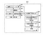
(2-1)機能ブロック
図8は、実施の形態2にかかるIDDQテスト用サイクル選択抽出装置300のブロック構成図である。論理シミュレーション部301は、以下に説明するテスト用サイクル選択抽出部303によるタイミング制御に基づいて、所定のハードウェア記述言語で記述されたCMOS集積回路の論理シミュレーションを実行し、1サイクル毎のシミュレーション結果を出力する。
【0053】
データ編集部302は、論理シミュレーション部301より送られてくる論理シミュレーションの結果及びCMOS集積回路の情報から、スタンバイサイクルにおいて、全部でM個ある内部ネットの内、有効に取り扱うm個の内部ネットを特定し、特定した各ネットの信号状態を表すmビットデータを出力する。なお、このデータ編集部302は、上記実施の形態1のIDDQテスト用サイクル選択抽出装置150内に備えられるデータ編集部151と同じ処理を実行するものであり、ここでの重複した説明は省略する。
【0054】
テスト用サイクル選択抽出部303は、データ編集部302を介して送られてくるスタンバイサイクルのmビットデータが、直前に選択抽出したサイクルのmビットデータと、ハミング距離に関して所定の条件を満足する場合にのみ、当該サイクルをIDDQテスト用のサイクルとして選択する。テスト用サイクル選択抽出部303は、この判断を行った後に、論理シミュレーション部301に対して、次のサイクルのシミュレーションを実行させる。
【0055】
処理終了条件入力部304は、上記テスト用サイクル選択抽出部303において実行するIDDQテスト用サイクルの選択抽出条件、及び、処理終了条件を外部より設定するためのマン・マシンインターフェースである。
【0056】
故障シミュレーション部307は、所定のテストパターンを用いて実行した故障シミュレーションの結果に基づいて、上記所定のテストパターンによりどこのネットにおいてどのような故障(”0”縮退故障又は”1”縮退故障)が検出されるのか、又は、どのネットではどのような故障を検出できないのかといった情報を未検出故障データ格納部306に出力する。
なお、故障シミュレーション部307は、図1に示した故障シミュレーション装置110と同じである。また、未検出故障データ格納部306は、上記実施の形態1のIDDQテスト用サイクル選択抽出装置150内の未検出故障データ格納部157と同じである。
【0057】
テスト用サイクル選択抽出部303において上記選択抽出処理を行う際には、ファンクションテストで検出される故障をテストサイクル選択抽出処理の対象外とする。このように、同一の故障に対して2重に故障検出が行われるのを排除してIDDQテストに要する時間を短縮する。
【0058】
未検出故障認識及びトグル認識レジスタ設定部305は、未検出故障データ格納部306に格納されている各ネットにおける故障についての情報に基づいて、トグル認識レジスタの設定を行う。トグル認識レジスタの設定処理の内容は、上記実施の形態1のIDDQテスト用サイクル選択抽出装置150内の備えられる未検出故障認識及びトグル認識レジスタ設定部156と同じ処理を実行するものであり、ここでの重複した説明は省略する。
【0059】
印刷・表示部308は、上記テスト用サイクル選択抽出部303により選択抽出された各サイクルについて、論理シミュレーションの開始より何番目のサイクルであるのかを表す情報を印刷又は表示する。
【0060】
(2-2)ハードウェア構成
図9は、IDDQテスト用サイクル選択抽出装置300のハードウェア構成を示す図である。本装置300は、キーボード400、マウス401、記憶装置402、データ処理装置403、ディスプレイ404、及び、プリンタ405より構成される。
【0061】
キーボード400及びマウス401は、図8に示した処理終了条件入力部304として機能する。記憶装置402は、図8に示した未検出故障データ格納部306として機能する。データ処理装置403は、中央演算処理装置(CPU)及びプログラムを格納するメモリより構成され、中央演算処理部がメモリに書き込まれているIDDQテスト用サイクル選択抽出処理プログラムを実行することで、図8に示したデータ編集部302、IDDQテスト用サイクルの選択抽出部303、及び、未検出故障認識及びトグル認識レジスタ設定部305として機能する。ディスプレイ404及びプリンタ405は、図8に示した印刷・表示部155として機能する。
【0062】
また、データ処理装置403の備えるメモリには、論理シミュレーションプログラム及び故障シミュレーションのプログラムが格納されている。データ処理装置403の備えるCPUは、必要に応じてこれらのプログラムを実行する。
【0063】
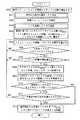
(2-3)IDDQテスト用サイクルの選択抽出処理
図10は、データ処理装置403の実行するIDDQテスト用サイクル選択抽出処理のフローチャートである。以下、本フローチャートに従ってIDDQテスト用のサイクルの選択抽出処理について説明する。
【0064】
まず、論理シミュレーション部301によるCMOS集積回路の論理シミュレーションを開始し、各動作サイクルにおける各ネットの状態より最初のスタンバイ状態を検出する(ステップS60)。論理シミュレーション部301から送られてくるCMOS集積回路の内部ネットについての情報に基づいて、有効に取り扱うm個のネットを特定し、各ネットの論理値を所定の順序で並べてmビットのデータとして出力する(ステップS61)。なお、この処理内容は、上記実施の形態1のデータ処理装置203の実行するステップS1の処理と同じであり、ここでの重複した説明は省く。
【0065】
所定のテストパターンを用いて故障シミュレーションを実行し、どのネットにおいてどんな故障(”0”縮退故障又は”1”縮退故障)が検出されたのか、又は、どのネットではどんな故障を検出することができなかったのかといった情報を取得する(ステップS62)。
【0066】
故障シミュレーションの実行後、トグル認識レジスタの設定を行う(ステップS63)。ここでは、ファンクションテストにより検出される故障をIDDQテストの対象外とするため、トグル済みフラグ記憶部及び未トグルデータ記憶部の各値を設定する。例えば、所定のテストパターンを用いた故障シミュレーションの結果より”0”縮退故障及び”1”縮退故障の両方の故障が検出されたネットについては、対応するトグル済みフラグの値を”1”にセットする。
なお、このトグル認識レジスタの構成は、実施の形態1のIDDQテスト用サイクル選択抽出装置150が用いるものと同じであり、図4に示すようにトグル済みフラグ記憶部250及び未トグルデータ記憶部251よりなり、データ処理装置403内に備えるメモリを用いて実現される。上記ステップS63において実行するトグル認識レジスタの設定処理は、図5及び図6を用いて説明したトグル認識レジスタの設定(図3、ステップS3)と同じであるため、ここでの重複した説明は省く。
【0067】
最初に検出されたスタンバイ状態におけるサイクルを第1のIDDQテスト用のサイクルとし、論理シミュレーションの開始より何番目のサイクルであるのかを特定する情報、第1番目にIDDQテスト用のサイクルとして選択抽出されたことを表すデータ、及び、このサイクルにおける各ネットの論理値を所定の順序で並べて表したmビットのデータを記憶装置402に保存すると共に、トグル認識レジスタ内に記憶するトグル済みフラグ及び未トグルデータの値を更新する(ステップS64)。
【0068】
この後、論理シミュレーションを続行して1サイクル分時計を進め(ステップS65)、次のサイクルがスタンバイ状態であるか否かについての判断を行う(ステップS66)。ここで、論理シミュレーションを実行したサイクルがスタンバイサイクルでない場合(ステップS66でNO)、上記ステップS65に戻り、次のサイクルについての論理シミュレーションを実行する。
【0069】
論理シミュレーションを実行したサイクルがスタンバイサイクルの場合(ステップS66でYES)、当該サイクルにおけるmビットデータと、1つ前のタイミングでIDDQテスト用のサイクルであるとして選択抽出されたサイクルのmビットデータについて、トグル済みフラグの値が”0”のビット位置のデータに着目した場合のハミング距離が所定の基準値以上であるか否かについての判断を行う(ステップS67)。
【0070】
ここで、ハミング距離が所定値以上でない場合(ステップS67でNO)、上記ステップS65に戻り、次のサイクルについての論理シミュレーションを実行する。なお、上記所定の基準値は、mビットデータの内、トグル済みフラグが”0”のビットの数に応じて、所定の規則に従い変更する。例えば、トグル済みフラグが”0”のビット数がp(但し、m≧p)である場合、上記所定の基準値をp−2(但し、p≦2の場合には1)に設定する。
【0071】
一方、当該サイクルがスタンバイ状態にあると判断された場合であって(ステップS66でYES)、ハミング距離が上記所定の基準値以上の場合には(ステップS67でYES)、当該サイクルを次のIDDQテスト用のサイクルとして選択抽出し、当該サイクルが論理シミュレーションの開始より何番目のサイクルであるのかを特定するデータ、第1番目にIDDQテスト用のサイクルとして選択抽出されたことを表すデータ、及び、このサイクルにおける各ネットの論理値を所定の順序で並べて表したmビットのデータを記憶装置202に保存する(ステップS68)。
【0072】
トグル済みフラグの値が”0”のビット位置のデータに着目し、上記ステップS68で選択したIDDQテスト用のサイクルにおけるmビットデータと、その直前に選択したmビットデータとの比較を行い、トグル済みフラグの更新を行う(ステップS69)。
未処理のサイクルが存在する場合、又は、トグル済みフラグに”0”にセットされているビットが未だ存在している場合であって(ステップS70でYES)、操作者により設定された終了条件を未だ満足していない場合(ステップS71でNO)、上記ステップS65に戻り、次のサイクルについての処理を行う。
【0073】
一方、全てのサイクルに対する処理が終了した場合、又は、トグル済みフラグの全てが”1”にセットされた場合には(ステップS70でNO)、処理を終了し、ディスプレイ204及びプリンタ205等へ処理結果を出力するステップS72へと進む。また、未処理サイクルが残っている場合、又は、トグル済みフラグに”0”にセットされているビットが残存している場合であっても(ステップS70でYES)、操作者が指定した終了条件を満足した場合には(ステップS71でYES)、処理を終了し、ディスプレイ204及びプリンタ205等へ処理結果を出力するステップS72へと進む。ステップS72では、記憶装置202に保存したIDDQテスト用の各サイクルについて、論理シミュレーションの開始から何番目の動作サイクルであるのかを特定する情報(データ)をディスプレイ204に表示出力すると共に、プリンタ205により印刷出力する。
【0074】
以上に説明したように、実施の形態2にかかるIDDQテスト用サイクルの選択抽出装置300は、上記実施の形態1のIDDQテスト用サイクルの選択抽出装置150と同様にファンクションテストで検出される故障を処理対象外とすることで、短時間で必要十分な数のIDDQテスト用サイクルを選択抽出することができる。
また、実施の形態2にかかるIDDQテスト用サイクルの選択抽出装置300は、論理シミュレーション部301における論理シミュレーションの実行に連動してIDDQテスト用のサイクルを選択抽出するため、論理シミュレーションの終了と共に、IDDQテスト用サイクルの選択処理を終了する。これにより、実施の形態1にかかるIDDQテスト用サイクルの選択抽出装置150に比べて処理に要する時間を短くすることができる。
【0075】
【発明の効果】
請求項1記載のIDDQテスト用サイクル選択抽出装置、及び、請求項6記載の記録媒体に記録得してあるプログラムを実行することによりコンピュータ上に実現されるIDDQテスト用サイクル選択抽出装置では、所定のテストパターンを用いた故障シミュレーションの結果より、n個のスタンバイ状態のサイクルにおける各mビットデータの内、故障シミュレーション手段により特定される、故障が検出されたネットに対応する位置のビットデータを、IDDQテスト用サイクル選択抽出の処理対象外とすることで、効果的にIDDQテスト用サイクルの選択を行い、使用するmビットデータの数を低減し、テストに要する時間を短縮することができる。
【0076】
請求項2記載のIDDQテスト用サイクル選択抽出装置は、請求項1記載のIDDQテスト用サイクル選択抽出装置において、更に、n個のmビットデータの内、最もハミング距離の遠い2つのmビットデータを、最初に必ず選択することができ、最も効果的にIDDQテスト用サイクルの選択を行い、使用するmビットデータの数を低減し、テストに要する時間を短縮することができる。
【0077】
請求項3記載のIDDQテスト用サイクル選択抽出装置は、請求項1記載のIDDQテスト用サイクル選択抽出装置において、論理シミュレータによる論理シミュレーションの実行と連動して動作するため、論理シミュレーションの終了と同時にIDDQテスト用のサイクル選択抽出処理を終了することができる。このように、迅速に処理結果が得られるので、テストに要する時間を短縮することができる。
【0078】
請求項4又は請求項5に記載のIDDQテスト用サイクル選択抽出装置は、処理終了条件としてトグル済みフラグの数や選択したサイクルの数を定めておくことで、処理の迅速化を図ることができる。
【図面の簡単な説明】
【図1】 本発明の実施の形態1にかかるIDDQテスト用サイクル選択装置の機能ブロック図である。
【図2】 本発明の実施の形態1にかかるIDDQテスト用サイクル選択装置のハードウェア構成図である。
【図3】 データ処理装置の実行する処理を示すフローチャートである。
【図4】 トグル認識レジスタのデータ構成を示す図である。
【図5】 トグル認識レジスタの設定処理のフローチャートである。
【図6】 トグル認識レジスタの設定処理を具体的に説明するための図である。
【図7】 10個のmビットデータに対するデータ処理装置による処理例を示す図である。
【図8】 実施の形態2にかかるIDDQテスト用サイクル選択抽出装置の機能ブロックを示す図である。
【図9】 実施の形態2にかかるIDDQテスト用サイクル選択抽出装置のハードウェア構成図である。
【図10】 実施の形態2にかかるIDDQテスト用サイクル選択抽出装置の処理のフローチャートである。
【符号の説明】
100…論理シミュレーション装置
110…故障シミュレーション装置
150,300…IDDQテスト用サイクル選択抽出装置
151,302…データ編集部
152…スタンバイサイクルのmビットデータ格納部
153,304…処理終了条件入力部
154,303…IDDQテスト用サイクル選択抽出部
155,308…選択抽出済みサイクル印刷・表示部
156,305…未検出故障認識及びトグル認識レジスタ設定部
157,306…未検出故障データ格納部
200,400…キーボード
201,401…マウス
202,402…記憶装置
203,403…データ処理装置
204,404…ディスプレイ
205,405…プリンタ
250…トグル済みフラグ記憶部
251…未トグルデータ記憶部
301…論理シミュレーション部
307…故障シミュレーション部[0001]
BACKGROUND OF THE INVENTION
The present invention uses logic simulation to make the I of a semiconductor integrated circuit.DDQ The present invention relates to an apparatus for selectively extracting a test cycle and a method of selective extraction.
[0002]
[Prior art]
As the miniaturization and high integration of CMOS integrated circuits progress, the burden on the test process is rapidly increasing. In fact, the number of test patterns is increasing year by year. To complicate matters, new types of failures that are difficult to find in current mainstream function tests tend to increase. This new failure is, for example, an open failure or a failure that occurs only in a transient state during a switching operation.
For this reason, when only the function test is carried out, cases in which the new failure is included are shipped as non-defective products and are increasingly incorporated into devices.
[0003]
As a new test method for detecting a new failure that cannot be detected by the above function test, IDDQ Attention is focused on testing. IDDQ In the test, a minute power supply current flowing through a CMOS integrated circuit in a standby state is measured, and a failure is detected based on the magnitude of the current value. This utilizes the fact that in a normal CMOS circuit, only a small amount of power supply current flows in the standby state. That is, when a large amount of current flows through the CMOS circuit in the standby state, it means that the circuit includes some defect (failure). During the operation of a normal integrated circuit, its internal state changes from moment to moment. Of each cycle during operation, the cycle realizing the standby state is detected, and the standby current in the detected cycle is measured.DDQ A test can be performed.
[0004]
By the way, a technique for knowing whether or not a standby state is realized in a certain cycle by using logic simulation is well known. For example, in Japanese Patent Laid-Open No. 4-44172, it is assumed that the standby state in which the power supply current is to be measured is when the following four conditions are satisfied.
(1) The output signals of a plurality of gates are not in a conflicting state (bus conflict).
(2) All gate outputs connected to the bus are not in a high impedance “Z” state.
(3) The logical value of the node with pull-up is “H”.
(4) The logical value of the node with a pull-down is “L”.
[0005]
[Problems to be solved by the invention]
If only the quality of the test (= failure detection capability by that test) is taken into consideration, it is better to perform the test in various internal conditions as much as possible. Therefore, it is most desirable to perform a test for every cycle in which the standby state is realized. However, in practice, since the test time directly affects the manufacturing cost, it is required to shorten the test time as much as possible while maintaining the test quality at a certain level.
[0006]
IDDQ The test measures current. Since current measurement generally takes longer than voltage measurement, it is desirable to reduce the number of current measurements in order to shorten the test time. This requires selecting and extracting enough standby cycles as necessary to maintain test quality, rather than testing in all standby cycles.
[0007]
As already described, a so-called function test for testing a functional operation of a semiconductor integrated circuit actually manufactured is always performed. However, in this function test, a part of the detected fault is an I to be performed to supplement the function test.DDQ It may also be detected in tests.
[0008]
However, the conventional test apparatus does not consider anything about this, and IDDQ In the test, a test cycle (or test pattern) is selected and extracted with all failures as targets. For this reason, the following problems arise.
[0009]
First, the test time of the semiconductor integrated circuit becomes unnecessarily long. This directly increases the cost of the semiconductor integrated circuit.
Second, IDDQ The time for which the test apparatus is occupied by one semiconductor integrated circuit becomes unnecessarily long. This deteriorates the development efficiency of the semiconductor integrated circuit during development, resulting in an increase in the cost of the semiconductor integrated circuit.
[0010]
The present invention has been made to solve the above-described problems of the conventional apparatus, and it is necessary to target only a failure that is not detected by the function test.DDQ An object of the present invention is to provide an apparatus for quickly selecting and extracting a test cycle.
[0011]
[Means for Solving the Problems]
I according to
[0012]
I of claim 2 of the present inventionDDQ A test cycle selective extraction apparatus according to
[0013]
I according to claim 3DDQ A test cycle selective extraction apparatus according to
[0014]
I according to claim 4DDQ The cycle selective extraction device for test is the I or 2 according to claim 2 or
[0015]
I according to
[0016]
In order to solve the above-mentioned problems, a computer according to
[0017]
DETAILED DESCRIPTION OF THE INVENTION
I of the present inventionDDQ The test cycle selection device targets only faults that cannot be detected by the function test.DDQ It is characterized by executing a test.
Hereinafter, I having the above characteristicsDDQ An embodiment of a test cycle selective extraction apparatus will be described with reference to the accompanying drawings.
[0018]
(1)
(1-1) Function block
FIG. 1 shows I according to the first embodiment.DDQ 3 is a block configuration diagram of a test cycle selection and
The
[0019]
Similarly, the failure simulation device 110 provided as an external device executes a failure simulation using a predetermined test pattern, and what kind of failure (“0” stuck-at fault or “1” stuck-at failure) occurs in any net. ) Is detected, or information indicating what kind of failure cannot be detected in which net is output to the undetected failure
[0020]
IDDQ In the test cycle selection /
[0021]
Here, the
[0022]
IDDQ The internal net to be handled as the target of the test cycle selection / extraction process may be specified directly based on the operator's settings, or in units (functional blocks, hierarchical structures, power supply systems) partitioned based on predetermined rules. May be specified. The M internal nets existing in the logic circuit can be specified based on the description data of the logic circuit provided in the
[0023]
The m-bit
[0024]
The process end
[0025]
The undetected failure recognition and toggle recognition
[0026]
The m-bit
[0027]
The print /
[0028]
(1-2) Hardware configuration
FIG.DDQ It is a figure which shows the hardware constitutions of the
[0029]
The
The
The
The
[0030]
(1-3) IDDQ Selective extraction process for test cycle
FIG. 3 shows I executed by the
[0031]
First, based on the information about the internal net of the CMOS integrated circuit to be processed sent from the
[0032]
From the result of the logic simulation for the CMOS integrated circuit to be processed, n standby states existed during the operation cycle (the number varies depending on the scale of the circuit, etc.) for the m internal nets identified in step S1. And the logical values of the nets in the detected cycle are arranged in a predetermined order to form m-bit data, and then stored in the storage device 202 (step S2).
[0033]
The n number of m-bit data includes the data specifying the number of operation cycles from the start of the logic simulation and the first to first in order of appearance timing for convenience of the following processing. The identification number of n is assigned and stored in the
Since a technique for determining whether or not a standby state is realized in a certain operation cycle is well known (for example, Japanese Patent Laid-Open No. 4-44172), description thereof is omitted here.
[0034]
Next, the toggle recognition register is set (step S3). As shown in FIG. 4, the toggle recognition register is a register of 2 × m bits in total, in which m-bit (up to M bits) toggled flag storage unit 250 and non-toggle data storage unit 251 are arranged. This is realized using a memory provided in the
In step S3, a failure detected by a function test executed later is IDDQ Each value of the toggled flag storage unit 250 and the non-toggle data storage unit 251 is set so as not to be tested. For example, the value of the corresponding toggled flag is set to “1” for a net in which both “0” stuck-at fault and “1” stuck-at fault are detected from the result of the fault simulation performed using a predetermined test pattern. set.
The contents of the process will be described in detail later.
[0035]
Of the already selected m-bit data, the value of the flag stored in the toggled flag storage unit 250 in the toggle recognition register is “0”, and the data stored in the untoggled data storage unit 251 Focus on data whose value is “0” or “1” (hereinafter referred to as untoggling data).
Select the m-bit data with the longest Hamming distance for the untoggled data and the data configured by arranging the data at the bit positions corresponding to the untoggled data from the plurality of m-bit data that have not yet been selected and extracted. Extract (step S4).
[0036]
The contents of the process in step S4 will be supplementarily described. For example, the content of the toggled flag storage unit 250 set in the setting of the toggle recognition register (step S3) is “1111... 000”, and the content of the non-toggle data storage unit 251 is “XXXX. X represents undefined data). Information that the corresponding bit is unconfirmed data X is recorded in a memory provided in the
Here, for convenience of explanation, assuming that the toggled flag is “1” for all the data of “...”, The non-toggled data becomes 3-bit data “001”.
In step S4, the m-bit data having the largest hamming distance with respect to the 3-bit data configured by arranging the data at the corresponding bit positions of the untoggled data “001” has not yet been selected and extracted. Select and extract from a plurality of m-bit data. For example, when m-bit data such as “ΔΔΔΔ... 110” (where Δ is arbitrary data) exists, this m-bit data is selectively extracted.
[0037]
The comparison with the m-bit data selected and extracted in step S4 is performed, and the flag value of the corresponding bit in the toggled flag storage unit 250 in the toggle recognition register is updated for the remaining bits (step S5). Note that the value of the bit that was the indeterminate data X at the time of updating is set as the value of the corresponding bit of the m-bit data selected and extracted in step S4. Among the toggled flags stored in the toggled flag storage unit 250 in the toggle recognition register, there are bits that are not yet set to 1 or m bits of n m-bit data that have not yet been selected and extracted. If data exists (YES in step S6), and if the processing end condition specified by the operator is not satisfied (NO in step S7), the process returns to step S4 and the process is continued.
[0038]
On the other hand, when all the values of the toggled flag stored in the toggled flag 250 in the toggle recognition register are set to 1, or when all the n m-bit data are selected and extracted (in step S6). NO), the process ends, and the process proceeds to step S8 for executing the process result output process.
Even in the case of YES in step S6, when a predetermined processing end condition designated by the operator via the input unit of the
[0039]
(1-4) Toggle recognition register setting processing
FIG. 5 is a flowchart of the toggle recognition register setting process (FIG. 3, step S3). FIG. 6 is a diagram illustrating an example of setting of the toggle recognition register. Hereinafter, the processing contents will be described according to the flow with reference to FIG.
[0040]
First, the toggle recognition register is initialized (step S31). In this initialization, all the m-bit data in the toggled flag storage unit 250 and the untoggled data storage unit 251 are set as unconfirmed data X (see (a) of FIG. 6). Note that the memory included in the
[0041]
Next, the result of the fault simulation executed using a predetermined test pattern is read from the undetected fault data storage unit 157 (step S32). For a net in which both “0” stuck-at fault (stuck-at-0 fault) and “1” stuck-at fault (stuck-at-1 fault) are detected from the read data, IDDQ Since it is not necessary to detect the failure again in the test, the value of the toggled flag is set to “1” (step S33). For example, in the state shown in FIG. 6A, when the upper first and second bits of the m-bit data correspond to this, the value of the bit corresponding to these in the toggled flag storage unit 250 is set to “1”. (See FIG. 6B). Note that the values of the first and second bits of the untoggling data storage unit 251 remain undefined X.
[0042]
For a net in which neither “0” stuck-at fault nor “1” stuck-at fault has been detected from the data read in step S32, the I in the state where the net is set to “0” and “1”.DDQ Since it is necessary to perform a test, the value of the toggled flag of the corresponding bit is set to “0” in a state where the value of the corresponding untoggled data is set to the undetermined data X (step S34). For example, in the state shown in FIG. 6B, when the upper third and fourth bits of m-bit data correspond to this, the value of the toggled flag of these bits is set to “0” (FIG. 6). (See (c)).
[0043]
For a net in which only “0” stuck-at fault is detected from the data read in step S32, the I in the state where the net is set to “0” in order to detect “1” stuck-at fault.DDQ A test is necessary, and the value of the data of the corresponding bit is set to “1”, and the value of the toggled flag of the corresponding bit is set to “0” (step S35). For example, in the state shown in FIG. 6C, when the lower third bit data of the m-bit data corresponds to this, the data of these bits is set to “1” and the toggled flag is set. The value is set to “0” (see (d) of FIG. 6).
[0044]
For a net in which only a “1” stuck-at fault is detected from the data read in step S32, the I in the state where the net is set to “1” in order to detect a “0” stuck-at fault.DDQ A test is necessary, and the value of the data of the corresponding bit is set to “0”, and the value of the toggled flag of the corresponding bit is set to “0” (step S36). For example, in the state shown in FIG. 6D, when the lower first and second bits of m-bit data correspond to this, the data of these bits is set to “0” and toggled. The value of the completed flag is set to “0” (see (e) of FIG. 6).
[0045]
By executing the above processing, a toggle recognition register that targets a failure other than the failure specified from the result of the failure simulation is set.
[0046]
(1-5) Specific examples
FIG. 7 shows a case where 10 m-bit data stored in the
[0047]
Assume that the toggle recognition register set in step S3 of the flowchart shown in FIG. 3 is in the state shown in FIG. In this case, in the process of step S4 to be executed next, the toggled flag is “0”, the data is “0” or “1”, and the toggle data “01. M-bit data having the largest Hamming distance with the data in which the bits to be arranged are arranged is selected. In this example, m-bit data with an identification number n = 5 is selected. By updating the toggle recognition flag in step S5, the updated toggle recognition flag becomes the state shown in (b). In this case, the value of the bit that was the indeterminate data X is replaced with the value of the corresponding bit of the m-bit data with the identification number n = 5.
[0048]
In the state shown in (b), the toggled flag “0” still has not yet toggled data (YES in step S6). In this case, if the user-specified end condition is not satisfied (NO in step S7), the m-bit data selection process (step S4) and the toggle recognition register update process (step S5) are repeatedly executed. To do. In the state shown in (b), the toggled flag is “0” and the untoggled data is “0” or “1” in which data “10” is arranged, and the corresponding bit is arranged in data. The m-bit data with the largest Hamming distance is m-bit data with an identification number n = 6. In step S4, m-bit data with an identification number n = 6 is selected. By selectively extracting this data, as shown in (c), the values of all the bits in the toggled flag storage unit 250 in the toggle recognition register are set to “1”.
[0049]
As described above, when all the m-bit values of the toggled flag storage unit 250 in the toggle recognition register are set to “1”, a cycle corresponding to these two m-bit data is set as I.DDQ The information is selected and extracted as a test cycle, and information (data) indicating the cycle number from the start of the logic simulation is displayed on the
[0050]
As described above, the I according to the first embodimentDDQ According to the test cycle selection / extraction device, of the n nets in the circuit in the n standby cycles obtained by executing the simulation by the
[0051]
(2) Embodiment 2
In the apparatus according to the first embodiment of the present invention, first, after logic simulation of the CMOS integrated circuit is executed by the
[0052]
(2-1) Function block
FIG. 8 shows I according to the second embodiment.DDQ 3 is a block configuration diagram of a test cycle selection and
[0053]
Based on the result of the logic simulation and the information of the CMOS integrated circuit sent from the
[0054]
The test cycle selection /
[0055]
The process end
[0056]
Based on the result of the fault simulation executed using the predetermined test pattern, the
The
[0057]
When the test cycle selection /
[0058]
The undetected failure recognition and toggle recognition
[0059]
The print /
[0060]
(2-2) Hardware configuration
FIG. 9 shows IDDQ It is a figure which shows the hardware constitutions of the cycle
[0061]
The
[0062]
The memory provided in the
[0063]
(2-3) IDDQ Selective extraction process for test cycle
FIG. 10 shows I executed by the
[0064]
First, logic simulation of the CMOS integrated circuit by the
[0065]
Fault simulation is executed using a predetermined test pattern, and what fault ("0" stuck fault or "1" stuck fault) is detected in which net, or what fault is detected in which net. Information such as whether or not there has been is acquired (step S62).
[0066]
After executing the fault simulation, the toggle recognition register is set (step S63). Here, the failure detected by the function test is IDDQ Each value of the toggled flag storage unit and the non-toggle data storage unit is set so as not to be tested. For example, for a net where both “0” stuck-at fault and “1” stuck-at fault are detected from the result of fault simulation using a predetermined test pattern, the value of the corresponding toggled flag is set to “1”. To do.
The configuration of this toggle recognition register is the same as that of the first embodiment.DDQ This is the same as that used by the test cycle selection /
[0067]
The first detected cycle in the standby state is the first IDDQ Information for identifying the cycle number for the test cycle from the start of the logic simulation, first IDDQ Data indicating that the cycle has been selected and extracted as a test cycle, and m-bit data in which the logical values of the nets in this cycle are arranged in a predetermined order are stored in the
[0068]
Thereafter, the logic simulation is continued to advance the clock by one cycle (step S65), and it is determined whether or not the next cycle is in a standby state (step S66). If the cycle in which the logic simulation is executed is not a standby cycle (NO in step S66), the process returns to step S65, and the logic simulation for the next cycle is executed.
[0069]
When the cycle in which the logic simulation is executed is a standby cycle (YES in step S66), the m-bit data in the cycle and the I timing at the previous timingDDQ Whether or not the Hamming distance is greater than or equal to a predetermined reference value when focusing on the data of the bit position where the value of the toggled flag is “0” for the m-bit data of the cycle selected and extracted as the test cycle Is determined (step S67).
[0070]
If the Hamming distance is not greater than or equal to the predetermined value (NO in step S67), the process returns to step S65, and a logic simulation for the next cycle is executed. The predetermined reference value is changed according to a predetermined rule according to the number of bits whose toggled flag is “0” in the m-bit data. For example, when the number of bits whose toggled flag is “0” is p (where m ≧ p), the predetermined reference value is set to p−2 (where p ≦ 2 is 1).
[0071]
On the other hand, if it is determined that the cycle is in the standby state (YES in step S66) and the hamming distance is equal to or greater than the predetermined reference value (YES in step S67), the cycle is changed to the next IDDQ Data that is selected and extracted as a test cycle and specifies the cycle number from the start of the logic simulation. First, IDDQ Data indicating that the test cycle has been selected and extracted and m-bit data in which the logical values of the nets in this cycle are arranged in a predetermined order are stored in the storage device 202 (step S68).
[0072]
Paying attention to the data at the bit position where the value of the toggled flag is “0”, the I selected in the above step S68.DDQ The m-bit data in the test cycle is compared with the m-bit data selected immediately before it, and the toggled flag is updated (step S69).
When there is an unprocessed cycle, or when a bit set to “0” in the toggled flag still exists (YES in step S70), the end condition set by the operator is set. If not satisfied yet (NO in step S71), the process returns to step S65 to perform processing for the next cycle.
[0073]
On the other hand, when the processing for all the cycles is completed, or when all the toggled flags are set to “1” (NO in step S70), the processing is terminated and processed to the
[0074]
As described above, the I according to the second embodimentDDQ The test cycle
In addition, I according to the second embodimentDDQ The test cycle selection /
[0075]
【The invention's effect】
I according to claim 1DDQ A cycle selection / extraction apparatus for testing, and an I implemented on a computer by executing a program recorded in the recording medium according to
[0076]
I according to claim 2DDQ A test cycle selective extraction apparatus according to
[0077]
I according to claim 3DDQ A test cycle selective extraction apparatus according to
[0078]
I according to claim 4 or
[Brief description of the drawings]
FIG. 1 is a diagram of an I according to a first embodiment of the present invention;DDQ It is a functional block diagram of the cycle selection apparatus for a test.
FIG. 2 is a diagram of I according to the first embodiment of the present invention;DDQ It is a hardware block diagram of the cycle selection apparatus for a test.
FIG. 3 is a flowchart showing processing executed by the data processing apparatus.
FIG. 4 is a diagram illustrating a data configuration of a toggle recognition register.
FIG. 5 is a flowchart of setting processing of a toggle recognition register.
FIG. 6 is a diagram for specifically explaining setting processing of a toggle recognition register.
FIG. 7 is a diagram illustrating an example of processing by a data processing apparatus for 10 m-bit data.
FIG. 8 is a diagram of an I according to the second embodiment.DDQ It is a figure which shows the functional block of the cycle selection extraction apparatus for a test.
FIG. 9 is a diagram illustrating an example I according to the second embodiment;DDQ It is a hardware block diagram of the cycle selection extraction device for a test.
FIG. 10 is a diagram of I according to the second embodiment;DDQ It is a flowchart of a process of the cycle selection extraction apparatus for a test.
[Explanation of symbols]
100: Logic simulation device
110 ... Failure simulation device
150, 300 ... IDDQ Test cycle extraction system
151, 302 ... Data editing section
152 ... m-bit data storage section for standby cycle
153, 304 ... Processing end condition input section
154,303 ... IDDQ Test cycle selection extraction unit
155, 308 ... Selected and extracted cycle print / display section
156, 305 ... Undetected fault recognition and toggle recognition register setting unit
157, 306 ... Undetected failure data storage unit
200,400 ... Keyboard
201, 401 ... mouse
202, 402 ... Storage device
203, 403 ... Data processing device
204, 404 ... display
205, 405 ... Printer
250: Toggle flag storage unit
251 ... Untoggling data storage unit
301 ... logic simulation section
307 ... Failure simulation section
Claims (6)
Translated fromJapanesen個のスタンバイ状態のサイクルにおけるmビットデータを保存するデータ保存手段と、
所定のテストパターンを用いて実行したCMOS集積回路の故障シミュレーションの結果に基づいて、テストパターンにより故障が検出されたネットを特定する故障シミュレーション手段と、
n個のスタンバイ状態のサイクルにおける各mビットデータの内、故障シミュレーション手段により特定される、故障が検出されたネットに対応する位置のビットデータを、IDDQテスト用サイクル選択抽出の処理対象外とする制御手段とを備えることを特徴とするIDDQテスト用サイクル選択抽出装置。Of the m-bit data representing the state of each of the m nets in the n standby cycles that appeared during the logic simulation of the CMOS integrated circuit, the values of all the bits constituting the m-bit data are at least once. "1" and the combination of m-bit data to be combined to be "0", a cycle selecting device for IDDQ test for selective extraction as cycle for IDDQ test,
data storage means for storing m-bit data in n standby cycles;
A failure simulation means for identifyinga netin which a failure is detected by the test pattern based on a result of the failure simulation of the CMOS integrated circuit executed using the predetermined test pattern;
Of the m-bit data in the n standby cycles, the bit data at the position corresponding to the net where the failure is detected, which is specified by the failure simulation means, is excluded from the processing target of cycle selection extraction for theIDDQ test. And a cycle selection and extraction device forIDDQ test.
mビットデータが順次与えられ、与えられたmビットデータに基づいてトグル済みフラグを更新する更新手段であって、新たに与えられたmビットデータと、その前に与えられたmビットデータとに関し、未だトグル済みフラグのセットされていない位置のビットデータ同士の比較を行い、一方が“1”で他方が“0”のデータ値を持つビットデータについてはトグル済みフラグをセットするフラグ更新手段と、
データ保存手段に記憶するn個のmビットデータの内、トグル済みフラグのセットされていない位置のビットデータ同士に着目し、互いのハミング距離の最も遠い2つのmビットデータを選択し、選択した2つのmビットデータを、第1及び第2のIDDQテスト用のサイクルのmビットデータとして、順にフラグ更新手段に与える第1データ選択手段と、
フラグ更新手段によるトグル済みフラグの更新後、mビットデータの内、未だトグル済みフラグがセットされていないビットデータの位置を認識する認識手段と、
認識手段により未だトグル済みフラグがセットされていないと認識された位置のビットデータだけに着目して、既に選択抽出されたIDDQテスト用のサイクルのmビットデータとのハミング距離が最も遠く、かつ、未だ選択されていないIDDQテスト用のサイクルのmビットデータを、データ保存手段に保存されているmビットデータ内から選択し、選択したmビットデータを、新たなIDDQテスト用のサイクルのmビットデータとして、フラグ更新手段に与える第2データ選択手段とを備え、
制御手段は、第1データ選択手段が2つのmビットデータを選択する前に、故障シミュレーション手段により故障が検出されたネットに対応するビット位置のトグル済みフラグをセットしてIDDQテスト用サイクル選択抽出の処理対象外とすることを特徴とする請求項1記載のIDDQテスト用サイクル選択抽出装置。Storage means for storing m toggled flags corresponding to each bit constituting m-bit data on a one-to-one basis;
m-bit dataare sequentially applied, an updating means for updating the toggle flag based on the given m-bit data,and the newly given m-bitdata,relates the m-bit data supplied to the front A flag updating means for comparingbit data at positions where the toggled flag has notyet been set, and forbit data having a data value of “1” on one side and “0” on the other side; ,
Of the n m-bit data stored in the data storagemeans,focusing on the bit data to each other at a position not set the toggle flagto select thefarthest two m-bit dataof the Hamming distance of eachother, selected First data selection means forsequentially givingtwo m-bit data to theflag update means as m-bit data ofthe first and secondIDQtest cycles ;
Recognizing means for recognizing the position of bit data in which the toggled flag has not been set among m-bit data after updating the toggled flag by the flag updating means;
Focusing only on the bit data at the position where the recognition means has not yet set the toggled flag, the Hamming distance from the m-bit data of the cycle for theIDDQ test that has been selected and extracted is the longest, and The m-bit data of the cycle for theIDDQ test not yet selected is selected from the m-bit data stored in the data storage means, and the selected m-bit data is selected for the cycle of the newIDDQ test. second data selection means to be provided to the flag update means as m-bit data,
The control meanssets the toggled flag of the bit position corresponding to the net where the failure is detected by the failure simulation means before the first data selection means selects thetwo m-bit data, and selects thecycle for theIDDQtest. 2. The cycle selection extraction apparatus forIDQQ test accordingto claim 1, wherein the extractiontarget is not subject to extraction processing.
論理シミュレーション手段によるシミュレーション実行時における動作サイクル毎に、当該サイクルに前記集積回路がスタンバイ状態にあるか否かを判断する判断手段と、
判断手段により最初にスタンバイ状態であると判断されたサイクルを第1のIDDQテスト用サイクルとして選択する第1サイクル選択手段と、
mビットのデータを構成する各ビットに一対一に対応するトグル済みフラグの記憶手段と、
第1サイクル選択手段による選択の後に、判断手段によりスタンバイ状態にあると判断されるサイクルの中から、上記選択された第1のIDDQテスト用のサイクルにおける上記CMOS集積回路内のm個のネットの状態を表すmビットのデータの内、トグル済みフラグのセットされていないビットの位置のみに着目した場合に、ハミング距離が上記着目するビットの数に応じて決まるしきい値よりも大きなmビットのデータを有する最初のサイクルを、第2のIDDQテスト用のサイクルとして選択する第2サイクル選択手段と、
第1及び第2サイクル選択手段により第1及び第2のIDDQテスト用として選択された2つのサイクルにおける回路内のm個のネットの状態を表す2つのmビットデータを保存するデータ保存手段と、
mビットデータが順次与えられ、与えられたmビットデータに基づいて、トグル済みフラグを更新する更新手段であって、新たに与えられたmビットデータ及びその前に与えられたmビットデータのトグル済みフラグのセットされていないビットのデータについて、ビット単位の比較を行い、一方が“1”で他方が“0”のデータ値を持つビットに対応するトグル済みフラグをセットするフラグ更新手段と、
データ保存手段に保存する2つのmビットデータを第1及び第2の選択抽出データとして選択し、順にフラグ更新手段に与える第1データ選択手段と、
フラグ更新手段によるトグル済みフラグの更新後、未だトグル済みフラグがセットされていないビットデータの位置を認識する認識手段と、
既に選択したmビットデータの内、認識手段により未だトグル済みフラグがセットされていないと認識されたビット位置のみに着目し、判断手段によりスタンバイ状態であると判断されたサイクルであって、上記着目するビット位置でのハミング距離が上記しきい値よりも大きいmビットデータを示すサイクルを選択し、選択したサイクルのmビットデータを、フラグ更新手段に与える第2データ選択手段とを備え、
制御手段は、第1データ選択手段による選択の前に、故障シミュレーション手段により故障が検出されたネットに対応するビット位置のトグル済みフラグをセットしてIDDQテスト用サイクル選択抽出の処理対象外とすることを特徴とする請求項1記載のIDDQテスト用サイクル選択抽出装置。A logic simulation means for executing a logic simulation of the CMOS integrated circuit;
For each operation cycle at the time of simulation execution by the logic simulation means, a determination means for determining whether or not the integrated circuit is in a standby state in the cycle;
First cycle selection means for selecting, as a firstIDQQ test cycle, a cycle first determined to be in a standby state by the determination means;
means for storing a toggled flag corresponding to each bit constituting m-bit data;
After the selection by the first cycle selection means,m nets in the CMOS integrated circuit in the selected cycle for the firstIDDQ test among the cycles determined by the determination means as being in the standby state. Of the m-bit data representing the state of, when focusing only on the position of the bit for which the toggled flag is not set, the m-bit is larger than the threshold value determined by the number of the focused bits. Second cycle selection means for selecting the first cycle having the following data as a cycle for the secondIDDQ test;
Data storage means for storing two m-bit data representing the states of m nets in the circuit in the two cycles selected for the first and secondIDQ tests by the first and second cycle selection means; ,
m-bit data is sequentially given, and updating means for updating a toggled flag based on the given m-bit data, wherein the newly given m-bit data and the toggle of the previously given m-bit data Flag updating means for performing bit-by-bit comparison on bit data for which a completed flag is not set, and setting a toggled flag corresponding to a bit having a data value of one being “1” and the other being “0”;
A first data selection unit that selects two m-bit data to be stored in the data storage unit as the first and second selection extraction data, andsequentially gives to the flag update unit;
Recognizing means for recognizing the position of bit data for which the toggled flag has not been set yet, after updating the toggled flag by the flag updating means;
Of the m-bit data that has already been selected, focus only on the bit position that has been recognized by the recognition means that the toggled flag has not yet been set, and the cycle determined by the determination means to be in the standby state, A second data selection unit that selects a cycle indicating m-bit data in which the Hamming distance at the bit position is larger than thethreshold value and supplies the m-bit data of the selected cycle to the flag update unit;
Before the selection by the first data selection means, the control meanssets a toggled flag at the bit position corresponding to the net where the failure is detected by the failure simulation means, so that thecycle selection extraction process for theIDDQtest is excluded. The cycle selective extraction apparatus forIDDQ testing accordingto claim 1, wherein:
コンピュータを
上記n個のスタンバイ状態のサイクルにおける各m個のネットの状態を表すmビットデータを保存するデータ保存手段と、
所定のテストパターンを用いて実行した上記CMOS集積回路の故障シミュレーションの結果に基づいて、テストパターンにより故障が検出されたネットを特定する故障シミュレーション手段と、
n個のスタンバイ状態のサイクルにおける各mビットデータの内、故障シミュレーション手段により特定される、故障が検出されたネットに対応する位置のビットデータを、IDDQテスト用サイクル選択抽出の処理対象外とする制御手段と、
して機能させるためのIDDQテスト用サイクル選択抽出処理プログラムを記録したコンピュータ読み取り可能な記録媒体。The computer has at least the values of all bits constituting m-bit data out of m-bit data representing the state of each of m nets in n standby cycles appearing during the logic simulation of the CMOS integrated circuit. once selected extracts a combination becomes "1" and "0", selected extracted m-bit data IDDQ test cycle selecting performs the selection extraction processing as the cycle for cycle IDDQ test corresponding to the extracted A recording medium on which anIDDQ test cycle selection extraction processing program for functioning as an apparatus is recorded,
Computer
Data storage means for storing m-bit data representing the state of each of m nets in the n standby state cycles;
A failure simulation means for identifyinga netin which a failure is detected by atest pattern based on a result of a failure simulation of the CMOS integrated circuit executed using a predetermined test pattern;
Of the m-bit data in the n standby cycles, the bit data at the position corresponding to the net where the failure is detected, which is specified by the failure simulation means, is excluded from the processing target of cycle selection extraction for theIDDQ test. Control means to
A computer-readable recording medium on which is recorded anIDDQ test cycle selective extraction processing program for functioning.
Priority Applications (2)
| Application Number | Priority Date | Filing Date | Title |
|---|---|---|---|
| JP07025498AJP3669836B2 (en) | 1998-03-19 | 1998-03-19 | IDDQ test cycle selective extraction device |
| US09/270,109US6098187A (en) | 1998-03-19 | 1999-03-16 | Method for selecting operation cycles of a semiconductor IC for performing an IDDQ test by using a logical simulation and a fault simulation |
Applications Claiming Priority (1)
| Application Number | Priority Date | Filing Date | Title |
|---|---|---|---|
| JP07025498AJP3669836B2 (en) | 1998-03-19 | 1998-03-19 | IDDQ test cycle selective extraction device |
Publications (2)
| Publication Number | Publication Date |
|---|---|
| JPH11271399A JPH11271399A (en) | 1999-10-08 |
| JP3669836B2true JP3669836B2 (en) | 2005-07-13 |
Family
ID=13426248
Family Applications (1)
| Application Number | Title | Priority Date | Filing Date |
|---|---|---|---|
| JP07025498AExpired - Fee RelatedJP3669836B2 (en) | 1998-03-19 | 1998-03-19 | IDDQ test cycle selective extraction device |
Country Status (2)
| Country | Link |
|---|---|
| US (1) | US6098187A (en) |
| JP (1) | JP3669836B2 (en) |
Families Citing this family (8)
| Publication number | Priority date | Publication date | Assignee | Title |
|---|---|---|---|---|
| SG135905A1 (en)* | 2000-05-22 | 2007-10-29 | Seagate Technology Llc | Method of overflow-based defect management representation |
| US6807647B2 (en)* | 2000-09-28 | 2004-10-19 | Ando Electric Co., Ltd. | IC test system and storage medium for the same |
| CA2399670A1 (en)* | 2001-10-29 | 2003-04-29 | Donald Shaw | Method and apparatus for modeling and simulating the effects of bridge defects in integrated circuits |
| CA2360291A1 (en) | 2001-10-30 | 2003-04-30 | Benoit Nadeau-Dostie | Method and program product for designing hierarchical circuit for quiescent current testing and circuit produced thereby |
| US6862717B2 (en)* | 2001-12-17 | 2005-03-01 | Logicvision, Inc. | Method and program product for designing hierarchical circuit for quiescent current testing |
| US7747926B2 (en)* | 2006-05-02 | 2010-06-29 | Everspin Technologies, Inc. | Methods and apparatus for a memory device with self-healing reference bits |
| US8159255B2 (en)* | 2008-02-15 | 2012-04-17 | Qualcomm, Incorporated | Methodologies and tool set for IDDQ verification, debugging and failure diagnosis |
| US20110270548A1 (en)* | 2010-04-29 | 2011-11-03 | Qualcomm Incorporated | Automated verification and estimation of quiescent power supply current |
Family Cites Families (5)
| Publication number | Priority date | Publication date | Assignee | Title |
|---|---|---|---|---|
| US4763289A (en)* | 1985-12-31 | 1988-08-09 | International Business Machines Corporation | Method for the modeling and fault simulation of complementary metal oxide semiconductor circuits |
| JPH07159496A (en)* | 1993-10-12 | 1995-06-23 | At & T Global Inf Solutions Internatl Inc | Device and method for inspecting integrated circuit |
| KR100212608B1 (en)* | 1996-01-12 | 1999-08-02 | 가네꼬 히사시 | CMOS integrated circuit fault diagnosis device and diagnostic method |
| JP3018996B2 (en)* | 1996-07-29 | 2000-03-13 | 日本電気株式会社 | Failure location identification method |
| US5983381A (en)* | 1997-12-31 | 1999-11-09 | Nec Usa Inc. | Partitioning and reordering methods for static test sequence compaction of sequential circuits |
- 1998
- 1998-03-19JPJP07025498Apatent/JP3669836B2/ennot_activeExpired - Fee Related
- 1999
- 1999-03-16USUS09/270,109patent/US6098187A/ennot_activeExpired - Lifetime
Also Published As
| Publication number | Publication date |
|---|---|
| JPH11271399A (en) | 1999-10-08 |
| US6098187A (en) | 2000-08-01 |
Similar Documents
| Publication | Publication Date | Title |
|---|---|---|
| JP3094448B2 (en) | Semiconductor device inspection method, device and manufacturing method | |
| JP4174167B2 (en) | Failure analysis method and failure analysis apparatus for semiconductor integrated circuit | |
| US5546408A (en) | Hierarchical pattern faults for describing logic circuit failure mechanisms | |
| US7308660B2 (en) | Calculation system of fault coverage and calculation method of the same | |
| JP4881332B2 (en) | Semiconductor integrated circuit test quality evaluation apparatus and semiconductor integrated circuit test quality evaluation method | |
| JP3018996B2 (en) | Failure location identification method | |
| US7266741B2 (en) | Generation of test vectors for testing electronic circuits taking into account of defect probability | |
| JP3669836B2 (en) | IDDQ test cycle selective extraction device | |
| JPH10283394A (en) | Fault simulation method | |
| US6449751B1 (en) | Method of analyzing static current test vectors with reduced file sizes for semiconductor integrated circuits | |
| JP2715956B2 (en) | Method for narrowing down a failure portion of CMOS logic circuit using Iddq | |
| US7202688B2 (en) | Output buffer circuit having signal path used for testing and integrated circuit and test method including the same | |
| US20040205436A1 (en) | Generalized fault model for defects and circuit marginalities | |
| JP3689537B2 (en) | IDDQ test cycle selective extraction device | |
| US6694495B1 (en) | Method of analyzing static current test vectors for semiconductor integrated circuits | |
| US5898705A (en) | Method for detecting bus shorts in semiconductor devices | |
| JP2008268062A (en) | Test pattern creation and failure detection rate calculation apparatus, test pattern creation and failure detection rate calculation method | |
| JPH1019986A (en) | Failure diagnosing equipment of cmos integrated circuit and failure diagnosing method | |
| JP2003107138A (en) | Test pattern selection device and test pattern selection method | |
| US7036063B2 (en) | Generalized fault model for defects and circuit marginalities | |
| JP2837703B2 (en) | Fault diagnosis device | |
| Chen et al. | Improving Efficiency of Cell-Aware Fault Modeling By Utilizing Defect-Free Analog Simulation | |
| JP2800755B2 (en) | Fault diagnosis device and diagnosis method for CMOS integrated circuit | |
| JPH10247208A (en) | Test method and test apparatus for integrated circuit | |
| JP2778556B2 (en) | Test pattern selection system |
Legal Events
| Date | Code | Title | Description |
|---|---|---|---|
| A977 | Report on retrieval | Free format text:JAPANESE INTERMEDIATE CODE: A971007 Effective date:20040423 | |
| A131 | Notification of reasons for refusal | Free format text:JAPANESE INTERMEDIATE CODE: A131 Effective date:20040928 | |
| A521 | Request for written amendment filed | Free format text:JAPANESE INTERMEDIATE CODE: A523 Effective date:20041129 | |
| TRDD | Decision of grant or rejection written | ||
| A01 | Written decision to grant a patent or to grant a registration (utility model) | Free format text:JAPANESE INTERMEDIATE CODE: A01 Effective date:20050405 | |
| A61 | First payment of annual fees (during grant procedure) | Free format text:JAPANESE INTERMEDIATE CODE: A61 Effective date:20050412 | |
| R150 | Certificate of patent or registration of utility model | Free format text:JAPANESE INTERMEDIATE CODE: R150 | |
| FPAY | Renewal fee payment (event date is renewal date of database) | Free format text:PAYMENT UNTIL: 20080422 Year of fee payment:3 | |
| FPAY | Renewal fee payment (event date is renewal date of database) | Free format text:PAYMENT UNTIL: 20090422 Year of fee payment:4 | |
| FPAY | Renewal fee payment (event date is renewal date of database) | Free format text:PAYMENT UNTIL: 20100422 Year of fee payment:5 | |
| FPAY | Renewal fee payment (event date is renewal date of database) | Free format text:PAYMENT UNTIL: 20100422 Year of fee payment:5 | |
| FPAY | Renewal fee payment (event date is renewal date of database) | Free format text:PAYMENT UNTIL: 20110422 Year of fee payment:6 | |
| FPAY | Renewal fee payment (event date is renewal date of database) | Free format text:PAYMENT UNTIL: 20120422 Year of fee payment:7 | |
| FPAY | Renewal fee payment (event date is renewal date of database) | Free format text:PAYMENT UNTIL: 20130422 Year of fee payment:8 | |
| FPAY | Renewal fee payment (event date is renewal date of database) | Free format text:PAYMENT UNTIL: 20140422 Year of fee payment:9 | |
| LAPS | Cancellation because of no payment of annual fees |