JP3669138B2 - Plasma CVD method, plasma CVD apparatus and electrode - Google Patents
Plasma CVD method, plasma CVD apparatus and electrodeDownload PDFInfo
- Publication number
- JP3669138B2 JP3669138B2JP05365998AJP5365998AJP3669138B2JP 3669138 B2JP3669138 B2JP 3669138B2JP 05365998 AJP05365998 AJP 05365998AJP 5365998 AJP5365998 AJP 5365998AJP 3669138 B2JP3669138 B2JP 3669138B2
- Authority
- JP
- Japan
- Prior art keywords
- article
- electrode
- plasma
- shape
- film
- Prior art date
- Legal status (The legal status is an assumption and is not a legal conclusion. Google has not performed a legal analysis and makes no representation as to the accuracy of the status listed.)
- Expired - Fee Related
Links
- 238000005268plasma chemical vapour depositionMethods0.000titleclaimsdescription96
- 239000012530fluidSubstances0.000claimsdescription55
- 230000015572biosynthetic processEffects0.000claimsdescription40
- 239000002994raw materialSubstances0.000claimsdescription25
- -1fluorocarbon compoundChemical class0.000claimsdescription18
- OKTJSMMVPCPJKN-UHFFFAOYSA-NCarbonChemical compound[C]OKTJSMMVPCPJKN-UHFFFAOYSA-N0.000claimsdescription14
- 229910052799carbonInorganic materials0.000claimsdescription13
- 229910001285shape-memory alloyInorganic materials0.000claimsdescription12
- 238000006243chemical reactionMethods0.000claimsdescription10
- 150000002430hydrocarbonsChemical class0.000claimsdescription9
- 238000004804windingMethods0.000claimsdescription9
- 239000007772electrode materialSubstances0.000claimsdescription6
- 239000004020conductorSubstances0.000claimsdescription3
- 238000002425crystallisationMethods0.000claims1
- 230000008025crystallizationEffects0.000claims1
- 238000007599dischargingMethods0.000claims1
- 239000010408filmSubstances0.000description175
- 239000007789gasSubstances0.000description109
- 238000000034methodMethods0.000description17
- 239000007788liquidSubstances0.000description15
- 238000000151depositionMethods0.000description14
- 230000008021depositionEffects0.000description14
- 239000000463materialSubstances0.000description13
- 239000002245particleSubstances0.000description13
- 229920005989resinPolymers0.000description13
- 239000011347resinSubstances0.000description13
- WMIYKQLTONQJES-UHFFFAOYSA-NhexafluoroethaneChemical compoundFC(F)(F)C(F)(F)FWMIYKQLTONQJES-UHFFFAOYSA-N0.000description12
- VNWKTOKETHGBQD-UHFFFAOYSA-NmethaneChemical compoundCVNWKTOKETHGBQD-UHFFFAOYSA-N0.000description12
- 239000000843powderSubstances0.000description11
- 230000004888barrier functionEffects0.000description10
- 229920001971elastomerPolymers0.000description10
- 239000005060rubberSubstances0.000description10
- 229910045601alloyInorganic materials0.000description9
- 239000000956alloySubstances0.000description9
- 238000010586diagramMethods0.000description9
- 230000000694effectsEffects0.000description9
- 238000002156mixingMethods0.000description9
- 239000010935stainless steelSubstances0.000description8
- 229910001220stainless steelInorganic materials0.000description8
- 229910052782aluminiumInorganic materials0.000description6
- XAGFODPZIPBFFR-UHFFFAOYSA-NaluminiumChemical compound[Al]XAGFODPZIPBFFR-UHFFFAOYSA-N0.000description6
- QVGXLLKOCUKJST-UHFFFAOYSA-Natomic oxygenChemical compound[O]QVGXLLKOCUKJST-UHFFFAOYSA-N0.000description5
- 239000001301oxygenSubstances0.000description5
- 229910052760oxygenInorganic materials0.000description5
- XEEYBQQBJWHFJM-UHFFFAOYSA-NIronChemical compound[Fe]XEEYBQQBJWHFJM-UHFFFAOYSA-N0.000description4
- 230000003247decreasing effectEffects0.000description4
- NBVXSUQYWXRMNV-UHFFFAOYSA-NfluoromethaneChemical compoundFCNBVXSUQYWXRMNV-UHFFFAOYSA-N0.000description4
- QSHDDOUJBYECFT-UHFFFAOYSA-NmercuryChemical compound[Hg]QSHDDOUJBYECFT-UHFFFAOYSA-N0.000description4
- 229910052753mercuryInorganic materials0.000description4
- 239000007787solidSubstances0.000description4
- UHOVQNZJYSORNB-UHFFFAOYSA-NBenzeneChemical compoundC1=CC=CC=C1UHOVQNZJYSORNB-UHFFFAOYSA-N0.000description3
- 229920002943EPDM rubberPolymers0.000description3
- WSFSSNUMVMOOMR-UHFFFAOYSA-NFormaldehydeChemical compoundO=CWSFSSNUMVMOOMR-UHFFFAOYSA-N0.000description3
- HSFWRNGVRCDJHI-UHFFFAOYSA-Nalpha-acetyleneNatural productsC#CHSFWRNGVRCDJHI-UHFFFAOYSA-N0.000description3
- 230000000052comparative effectEffects0.000description3
- 238000001816coolingMethods0.000description3
- 230000007423decreaseEffects0.000description3
- 229910021385hard carbonInorganic materials0.000description3
- 230000006872improvementEffects0.000description3
- 229910000734martensiteInorganic materials0.000description3
- 229910052751metalInorganic materials0.000description3
- 239000002184metalSubstances0.000description3
- 229920002379silicone rubberPolymers0.000description3
- 229920002554vinyl polymerPolymers0.000description3
- FERIUCNNQQJTOY-UHFFFAOYSA-MButyrateChemical compoundCCCC([O-])=OFERIUCNNQQJTOY-UHFFFAOYSA-M0.000description2
- FERIUCNNQQJTOY-UHFFFAOYSA-NButyric acidNatural productsCCCC(O)=OFERIUCNNQQJTOY-UHFFFAOYSA-N0.000description2
- CURLTUGMZLYLDI-UHFFFAOYSA-NCarbon dioxideChemical compoundO=C=OCURLTUGMZLYLDI-UHFFFAOYSA-N0.000description2
- 229910017535Cu-Al-NiInorganic materials0.000description2
- 229910017773Cu-Zn-AlInorganic materials0.000description2
- YCKRFDGAMUMZLT-UHFFFAOYSA-NFluorine atomChemical compound[F]YCKRFDGAMUMZLT-UHFFFAOYSA-N0.000description2
- UFHFLCQGNIYNRP-UHFFFAOYSA-NHydrogenChemical compound[H][H]UFHFLCQGNIYNRP-UHFFFAOYSA-N0.000description2
- 239000005062PolybutadieneSubstances0.000description2
- 229920001328Polyvinylidene chloridePolymers0.000description2
- ATUOYWHBWRKTHZ-UHFFFAOYSA-NPropaneChemical compoundCCCATUOYWHBWRKTHZ-UHFFFAOYSA-N0.000description2
- PPBRXRYQALVLMV-UHFFFAOYSA-NStyreneChemical compoundC=CC1=CC=CC=C1PPBRXRYQALVLMV-UHFFFAOYSA-N0.000description2
- 229910004337Ti-NiInorganic materials0.000description2
- 229910011209Ti—NiInorganic materials0.000description2
- 239000006229carbon blackSubstances0.000description2
- 229920002301cellulose acetatePolymers0.000description2
- 230000008859changeEffects0.000description2
- 229910003460diamondInorganic materials0.000description2
- 239000010432diamondSubstances0.000description2
- 239000012777electrically insulating materialSubstances0.000description2
- 239000011737fluorineSubstances0.000description2
- 229910052731fluorineInorganic materials0.000description2
- 238000010438heat treatmentMethods0.000description2
- KHYBPSFKEHXSLX-UHFFFAOYSA-NiminotitaniumChemical compound[Ti]=NKHYBPSFKEHXSLX-UHFFFAOYSA-N0.000description2
- 239000000203mixtureSubstances0.000description2
- 230000035699permeabilityEffects0.000description2
- 229920000139polyethylene terephthalatePolymers0.000description2
- 239000005020polyethylene terephthalateSubstances0.000description2
- 239000002861polymer materialSubstances0.000description2
- 239000002244precipitateSubstances0.000description2
- 230000009467reductionEffects0.000description2
- 239000004945silicone rubberSubstances0.000description2
- 239000000126substanceSubstances0.000description2
- 229920003002synthetic resinPolymers0.000description2
- 239000000057synthetic resinSubstances0.000description2
- BFKJFAAPBSQJPD-UHFFFAOYSA-NtetrafluoroetheneChemical groupFC(F)=C(F)FBFKJFAAPBSQJPD-UHFFFAOYSA-N0.000description2
- MIZLGWKEZAPEFJ-UHFFFAOYSA-N1,1,2-trifluoroetheneChemical compoundFC=C(F)FMIZLGWKEZAPEFJ-UHFFFAOYSA-N0.000description1
- 229920000178Acrylic resinPolymers0.000description1
- 239000004925Acrylic resinSubstances0.000description1
- 239000004215Carbon black (E152)Substances0.000description1
- 229910017518Cu ZnInorganic materials0.000description1
- 229910017752Cu-ZnInorganic materials0.000description1
- 229910017943Cu—ZnInorganic materials0.000description1
- 239000004641Diallyl-phthalateSubstances0.000description1
- OTMSDBZUPAUEDD-UHFFFAOYSA-NEthaneChemical compoundCCOTMSDBZUPAUEDD-UHFFFAOYSA-N0.000description1
- 239000001856Ethyl celluloseSubstances0.000description1
- ZZSNKZQZMQGXPY-UHFFFAOYSA-NEthyl celluloseChemical compoundCCOCC1OC(OC)C(OCC)C(OCC)C1OC1C(O)C(O)C(OC)C(CO)O1ZZSNKZQZMQGXPY-UHFFFAOYSA-N0.000description1
- 229920000181Ethylene propylene rubberPolymers0.000description1
- KRHYYFGTRYWZRS-UHFFFAOYSA-MFluoride anionChemical compound[F-]KRHYYFGTRYWZRS-UHFFFAOYSA-M0.000description1
- 244000043261Hevea brasiliensisSpecies0.000description1
- 229910003310Ni-AlInorganic materials0.000description1
- 229920000459Nitrile rubberPolymers0.000description1
- 239000000020NitrocelluloseSubstances0.000description1
- 229920002292Nylon 6Polymers0.000description1
- CTQNGGLPUBDAKN-UHFFFAOYSA-NO-XyleneChemical compoundCC1=CC=CC=C1CCTQNGGLPUBDAKN-UHFFFAOYSA-N0.000description1
- 239000004341OctafluorocyclobutaneSubstances0.000description1
- 229910001252Pd alloyInorganic materials0.000description1
- ISWSIDIOOBJBQZ-UHFFFAOYSA-NPhenolChemical compoundOC1=CC=CC=C1ISWSIDIOOBJBQZ-UHFFFAOYSA-N0.000description1
- 229930182556PolyacetalNatural products0.000description1
- 239000004698PolyethyleneSubstances0.000description1
- 239000004721Polyphenylene oxideSubstances0.000description1
- 239000004743PolypropyleneSubstances0.000description1
- 239000004793PolystyreneSubstances0.000description1
- 239000004372Polyvinyl alcoholSubstances0.000description1
- XUIMIQQOPSSXEZ-UHFFFAOYSA-NSiliconChemical compound[Si]XUIMIQQOPSSXEZ-UHFFFAOYSA-N0.000description1
- 229910001007Tl alloyInorganic materials0.000description1
- 229920001807Urea-formaldehydePolymers0.000description1
- 229920006311Urethane elastomerPolymers0.000description1
- FJWGYAHXMCUOOM-QHOUIDNNSA-N[(2s,3r,4s,5r,6r)-2-[(2r,3r,4s,5r,6s)-4,5-dinitrooxy-2-(nitrooxymethyl)-6-[(2r,3r,4s,5r,6s)-4,5,6-trinitrooxy-2-(nitrooxymethyl)oxan-3-yl]oxyoxan-3-yl]oxy-3,5-dinitrooxy-6-(nitrooxymethyl)oxan-4-yl] nitrateChemical compoundO([C@@H]1O[C@@H]([C@H]([C@H](O[N+]([O-])=O)[C@H]1O[N+]([O-])=O)O[C@H]1[C@@H]([C@@H](O[N+]([O-])=O)[C@H](O[N+]([O-])=O)[C@@H](CO[N+]([O-])=O)O1)O[N+]([O-])=O)CO[N+](=O)[O-])[C@@H]1[C@@H](CO[N+]([O-])=O)O[C@@H](O[N+]([O-])=O)[C@H](O[N+]([O-])=O)[C@H]1O[N+]([O-])=OFJWGYAHXMCUOOM-QHOUIDNNSA-N0.000description1
- 229920000800acrylic rubberPolymers0.000description1
- 229920000122acrylonitrile butadiene styrenePolymers0.000description1
- 239000004676acrylonitrile butadiene styreneSubstances0.000description1
- QUDWYFHPNIMBFC-UHFFFAOYSA-Nbis(prop-2-enyl) benzene-1,2-dicarboxylateChemical compoundC=CCOC(=O)C1=CC=CC=C1C(=O)OCC=CQUDWYFHPNIMBFC-UHFFFAOYSA-N0.000description1
- 210000000988bone and boneAnatomy0.000description1
- 239000001273butaneSubstances0.000description1
- 229920005549butyl rubberPolymers0.000description1
- 150000001722carbon compoundsChemical class0.000description1
- 239000001569carbon dioxideSubstances0.000description1
- 229910002092carbon dioxideInorganic materials0.000description1
- 239000012159carrier gasSubstances0.000description1
- 229920001727cellulose butyratePolymers0.000description1
- 239000012461cellulose resinSubstances0.000description1
- 239000000919ceramicSubstances0.000description1
- 229920006235chlorinated polyethylene elastomerPolymers0.000description1
- 239000011248coating agentSubstances0.000description1
- 238000000576coating methodMethods0.000description1
- 239000011231conductive fillerSubstances0.000description1
- 229920001577copolymerPolymers0.000description1
- 229910052802copperInorganic materials0.000description1
- TVZPLCNGKSPOJA-UHFFFAOYSA-Ncopper zincChemical compound[Cu].[Zn]TVZPLCNGKSPOJA-UHFFFAOYSA-N0.000description1
- 239000006185dispersionSubstances0.000description1
- 238000006073displacement reactionMethods0.000description1
- 229920005558epichlorohydrin rubberPolymers0.000description1
- 239000003822epoxy resinSubstances0.000description1
- 229920001249ethyl cellulosePolymers0.000description1
- 235000019325ethyl celluloseNutrition0.000description1
- 125000002534ethynyl groupChemical group[H]C#C*0.000description1
- 239000000835fiberSubstances0.000description1
- 239000007888film coatingSubstances0.000description1
- 238000009501film coatingMethods0.000description1
- 229920001973fluoroelastomerPolymers0.000description1
- 239000007849furan resinSubstances0.000description1
- 239000011521glassSubstances0.000description1
- 239000008187granular materialSubstances0.000description1
- HCDGVLDPFQMKDK-UHFFFAOYSA-NhexafluoropropyleneChemical groupFC(F)=C(F)C(F)(F)FHCDGVLDPFQMKDK-UHFFFAOYSA-N0.000description1
- 229930195733hydrocarbonNatural products0.000description1
- 239000001257hydrogenSubstances0.000description1
- 229910052739hydrogenInorganic materials0.000description1
- 230000001771impaired effectEffects0.000description1
- 239000011261inert gasSubstances0.000description1
- 238000009434installationMethods0.000description1
- 150000002500ionsChemical class0.000description1
- 229910052742ironInorganic materials0.000description1
- 238000005461lubricationMethods0.000description1
- 239000011159matrix materialSubstances0.000description1
- 239000012528membraneSubstances0.000description1
- IJDNQMDRQITEOD-UHFFFAOYSA-Nn-butaneChemical compoundCCCCIJDNQMDRQITEOD-UHFFFAOYSA-N0.000description1
- OFBQJSOFQDEBGM-UHFFFAOYSA-Nn-pentaneNatural productsCCCCCOFBQJSOFQDEBGM-UHFFFAOYSA-N0.000description1
- 229920003052natural elastomerPolymers0.000description1
- 229920001194natural rubberPolymers0.000description1
- 229910052759nickelInorganic materials0.000description1
- 229920001220nitrocellulosPolymers0.000description1
- BCCOBQSFUDVTJQ-UHFFFAOYSA-NoctafluorocyclobutaneChemical compoundFC1(F)C(F)(F)C(F)(F)C1(F)FBCCOBQSFUDVTJQ-UHFFFAOYSA-N0.000description1
- 235000019407octafluorocyclobutaneNutrition0.000description1
- 239000013034phenoxy resinSubstances0.000description1
- 229920006287phenoxy resinPolymers0.000description1
- 229920001084poly(chloroprene)Polymers0.000description1
- 229920003229poly(methyl methacrylate)Polymers0.000description1
- 229920001197polyacetylenePolymers0.000description1
- 229920000058polyacrylatePolymers0.000description1
- 229920002239polyacrylonitrilePolymers0.000description1
- 229920006122polyamide resinPolymers0.000description1
- 229920002857polybutadienePolymers0.000description1
- 239000004417polycarbonateSubstances0.000description1
- 229920000515polycarbonatePolymers0.000description1
- 229920000647polyepoxidePolymers0.000description1
- 229920001225polyester resinPolymers0.000description1
- 239000004645polyester resinSubstances0.000description1
- 229920000570polyetherPolymers0.000description1
- 229920000573polyethylenePolymers0.000description1
- 239000004926polymethyl methacrylateSubstances0.000description1
- 229920006324polyoxymethylenePolymers0.000description1
- 229920001155polypropylenePolymers0.000description1
- 229920002223polystyrenePolymers0.000description1
- 229920002635polyurethanePolymers0.000description1
- 239000004814polyurethaneSubstances0.000description1
- 229920002689polyvinyl acetatePolymers0.000description1
- 239000011118polyvinyl acetateSubstances0.000description1
- 229920002451polyvinyl alcoholPolymers0.000description1
- 229920000915polyvinyl chloridePolymers0.000description1
- 239000004800polyvinyl chlorideSubstances0.000description1
- 239000005033polyvinylidene chlorideSubstances0.000description1
- 239000000047productSubstances0.000description1
- 239000001294propaneSubstances0.000description1
- 229910052710siliconInorganic materials0.000description1
- 239000010703siliconSubstances0.000description1
- 229920002050silicone resinPolymers0.000description1
- JMHCCAYJTTWMCX-QWPJCUCISA-Msodium;(2s)-2-amino-3-[4-(4-hydroxy-3,5-diiodophenoxy)-3,5-diiodophenyl]propanoate;pentahydrateChemical compoundO.O.O.O.O.[Na+].IC1=CC(C[C@H](N)C([O-])=O)=CC(I)=C1OC1=CC(I)=C(O)C(I)=C1JMHCCAYJTTWMCX-QWPJCUCISA-M0.000description1
- 239000012798spherical particleSubstances0.000description1
- ISXSCDLOGDJUNJ-UHFFFAOYSA-Ntert-butyl prop-2-enoateChemical classCC(C)(C)OC(=O)C=CISXSCDLOGDJUNJ-UHFFFAOYSA-N0.000description1
- TXEYQDLBPFQVAA-UHFFFAOYSA-NtetrafluoromethaneChemical compoundFC(F)(F)FTXEYQDLBPFQVAA-UHFFFAOYSA-N0.000description1
- 229920005992thermoplastic resinPolymers0.000description1
- 229920001187thermosetting polymerPolymers0.000description1
- 239000010409thin filmSubstances0.000description1
- 229920006337unsaturated polyester resinPolymers0.000description1
- 125000000391vinyl groupChemical group[H]C([*])=C([H])[H]0.000description1
- 239000008096xyleneSubstances0.000description1
Images


Classifications
- H—ELECTRICITY
- H01—ELECTRIC ELEMENTS
- H01J—ELECTRIC DISCHARGE TUBES OR DISCHARGE LAMPS
- H01J37/00—Discharge tubes with provision for introducing objects or material to be exposed to the discharge, e.g. for the purpose of examination or processing thereof
- H01J37/32—Gas-filled discharge tubes
- H01J37/32431—Constructional details of the reactor
- H01J37/32532—Electrodes
- C—CHEMISTRY; METALLURGY
- C23—COATING METALLIC MATERIAL; COATING MATERIAL WITH METALLIC MATERIAL; CHEMICAL SURFACE TREATMENT; DIFFUSION TREATMENT OF METALLIC MATERIAL; COATING BY VACUUM EVAPORATION, BY SPUTTERING, BY ION IMPLANTATION OR BY CHEMICAL VAPOUR DEPOSITION, IN GENERAL; INHIBITING CORROSION OF METALLIC MATERIAL OR INCRUSTATION IN GENERAL
- C23C—COATING METALLIC MATERIAL; COATING MATERIAL WITH METALLIC MATERIAL; SURFACE TREATMENT OF METALLIC MATERIAL BY DIFFUSION INTO THE SURFACE, BY CHEMICAL CONVERSION OR SUBSTITUTION; COATING BY VACUUM EVAPORATION, BY SPUTTERING, BY ION IMPLANTATION OR BY CHEMICAL VAPOUR DEPOSITION, IN GENERAL
- C23C16/00—Chemical coating by decomposition of gaseous compounds, without leaving reaction products of surface material in the coating, i.e. chemical vapour deposition [CVD] processes
- C23C16/44—Chemical coating by decomposition of gaseous compounds, without leaving reaction products of surface material in the coating, i.e. chemical vapour deposition [CVD] processes characterised by the method of coating
- C23C16/50—Chemical coating by decomposition of gaseous compounds, without leaving reaction products of surface material in the coating, i.e. chemical vapour deposition [CVD] processes characterised by the method of coating using electric discharges
- C—CHEMISTRY; METALLURGY
- C23—COATING METALLIC MATERIAL; COATING MATERIAL WITH METALLIC MATERIAL; CHEMICAL SURFACE TREATMENT; DIFFUSION TREATMENT OF METALLIC MATERIAL; COATING BY VACUUM EVAPORATION, BY SPUTTERING, BY ION IMPLANTATION OR BY CHEMICAL VAPOUR DEPOSITION, IN GENERAL; INHIBITING CORROSION OF METALLIC MATERIAL OR INCRUSTATION IN GENERAL
- C23C—COATING METALLIC MATERIAL; COATING MATERIAL WITH METALLIC MATERIAL; SURFACE TREATMENT OF METALLIC MATERIAL BY DIFFUSION INTO THE SURFACE, BY CHEMICAL CONVERSION OR SUBSTITUTION; COATING BY VACUUM EVAPORATION, BY SPUTTERING, BY ION IMPLANTATION OR BY CHEMICAL VAPOUR DEPOSITION, IN GENERAL
- C23C16/00—Chemical coating by decomposition of gaseous compounds, without leaving reaction products of surface material in the coating, i.e. chemical vapour deposition [CVD] processes
- C23C16/22—Chemical coating by decomposition of gaseous compounds, without leaving reaction products of surface material in the coating, i.e. chemical vapour deposition [CVD] processes characterised by the deposition of inorganic material, other than metallic material
- C23C16/26—Deposition of carbon only
- C—CHEMISTRY; METALLURGY
- C23—COATING METALLIC MATERIAL; COATING MATERIAL WITH METALLIC MATERIAL; CHEMICAL SURFACE TREATMENT; DIFFUSION TREATMENT OF METALLIC MATERIAL; COATING BY VACUUM EVAPORATION, BY SPUTTERING, BY ION IMPLANTATION OR BY CHEMICAL VAPOUR DEPOSITION, IN GENERAL; INHIBITING CORROSION OF METALLIC MATERIAL OR INCRUSTATION IN GENERAL
- C23C—COATING METALLIC MATERIAL; COATING MATERIAL WITH METALLIC MATERIAL; SURFACE TREATMENT OF METALLIC MATERIAL BY DIFFUSION INTO THE SURFACE, BY CHEMICAL CONVERSION OR SUBSTITUTION; COATING BY VACUUM EVAPORATION, BY SPUTTERING, BY ION IMPLANTATION OR BY CHEMICAL VAPOUR DEPOSITION, IN GENERAL
- C23C16/00—Chemical coating by decomposition of gaseous compounds, without leaving reaction products of surface material in the coating, i.e. chemical vapour deposition [CVD] processes
- C23C16/44—Chemical coating by decomposition of gaseous compounds, without leaving reaction products of surface material in the coating, i.e. chemical vapour deposition [CVD] processes characterised by the method of coating
- C23C16/50—Chemical coating by decomposition of gaseous compounds, without leaving reaction products of surface material in the coating, i.e. chemical vapour deposition [CVD] processes characterised by the method of coating using electric discharges
- C23C16/505—Chemical coating by decomposition of gaseous compounds, without leaving reaction products of surface material in the coating, i.e. chemical vapour deposition [CVD] processes characterised by the method of coating using electric discharges using radio frequency discharges
- C23C16/509—Chemical coating by decomposition of gaseous compounds, without leaving reaction products of surface material in the coating, i.e. chemical vapour deposition [CVD] processes characterised by the method of coating using electric discharges using radio frequency discharges using internal electrodes
- H—ELECTRICITY
- H01—ELECTRIC ELEMENTS
- H01J—ELECTRIC DISCHARGE TUBES OR DISCHARGE LAMPS
- H01J37/00—Discharge tubes with provision for introducing objects or material to be exposed to the discharge, e.g. for the purpose of examination or processing thereof
- H01J37/32—Gas-filled discharge tubes
- H—ELECTRICITY
- H01—ELECTRIC ELEMENTS
- H01J—ELECTRIC DISCHARGE TUBES OR DISCHARGE LAMPS
- H01J37/00—Discharge tubes with provision for introducing objects or material to be exposed to the discharge, e.g. for the purpose of examination or processing thereof
- H01J37/32—Gas-filled discharge tubes
- H01J37/32009—Arrangements for generation of plasma specially adapted for examination or treatment of objects, e.g. plasma sources
Landscapes
- Chemical & Material Sciences (AREA)
- Engineering & Computer Science (AREA)
- Physics & Mathematics (AREA)
- Plasma & Fusion (AREA)
- Analytical Chemistry (AREA)
- Materials Engineering (AREA)
- Chemical Kinetics & Catalysis (AREA)
- Mechanical Engineering (AREA)
- Metallurgy (AREA)
- Organic Chemistry (AREA)
- General Chemical & Material Sciences (AREA)
- Inorganic Chemistry (AREA)
- Chemical Vapour Deposition (AREA)
Description
Translated fromJapanese【0001】
【発明の属する技術分野】
本発明は、開口部を有する中空物品の外表面に成膜するためのプラズマCVD法、この方法に用いることができるプラズマCVD装置及び電極に関する。
【0002】
【従来の技術】
食品分野や医薬品分野等で用いられる容器の材料として樹脂が多用されている。樹脂製品は軽量で耐衝撃性に優れ、さらに安価であること等の利点を有する。ところが、樹脂製の容器はガスバリア性が悪いために内容物が酸化したり、内容物に含まれる2酸化炭素ガス等のガスが外部に放出され易いという難点を有する。また、比較的軟質であることから他物品との接触により傷が付き易い。
【0003】
このため、近年DLC膜等の硬質な炭素膜の優れた耐摩耗性、ガスバリア性等の特性に着目して、樹脂容器の表面に硬質な炭素膜を形成することが試みられている。
例えば特開平8−53117号公報によると、容器の外形と略相似形で該容器より若干大きい空所を有する中空状の外部電極内に膜形成すべき容器を設置し、該容器内に該容器の口部から挿入可能な細いロッド状の内部電極を挿入、設置して、該内部電極をガスノズルとして用いて該容器内部に成膜原料ガスを導入するとともに該両電極間にガスプラズマ化用の高周波電力を供給することで、該容器内表面に炭素膜を形成する方法及び装置が開示されている。また、この方法及び装置を用いると、容器の外表面に沿った形の外部電極に負の自己バイアスが発生して該容器内表面に均一に成膜できるとしている。また、放電領域が狭いため効率良く排気を行えるとともに成膜原料ガスが少なくて済み、生産性が良好であるとしている。
【0004】
また、容器状の被成膜物品の外表面に炭素膜等の膜を形成するための装置としては、図9に示すようなプラズマCVD装置が用いられている。この装置は、排気装置11が接続された真空チャンバ1を有し、該チャンバ1は接地電位とされる。該チャンバ1内には複数のロッド状の内部電極21が導電性の支持部材21’上に立設されたものが設置されている。内部電極21及び導電性支持部材21’はチャンバ1と電気的に絶縁されている。内部電極21には支持部材21’を介してマッチングボックス22及び高周波電源23がこの順に接続されている。また、真空チャンバ1には成膜原料ガスのガス供給部3が接続されている。ガス供給部3には、マスフロ−コントロ−ラ、弁及びガス源が含まれるが、これらは図示を省略している。
【0005】
この装置を用いて、容器状の被成膜物品Sすなわち開口部を有する中空物品Sの外表面に成膜するにあたっては、被成膜物品Sをチャンバ1内に搬入し、内部電極21に被せてこれに支持させる。次いで、排気装置11の運転にてチャンバ1内を所定圧力に減圧し、ガス供給部3からチャンバ1内へ成膜原料ガスを導入するとともに、高周波電源23からマッチングボックス22を介して内部電極21にガスプラズマ化用の高周波電力を供給し、前記導入した原料ガスをプラズマ化する。このプラズマの下で容器状の被成膜物品Sの外表面に成膜が行われる。なお、1バッチで内部電極21の数に応じた数の被成膜物品Sの成膜処理を行える。
【0006】
【発明が解決しようとする課題】
しかしながら、前記特開平8−53117号公報が教えるプラズマCVD法及び装置によると、容器内表面に炭素膜を形成するため他物品との接触による損傷防止効果は得られない。
また、前記図9のプラズマCVD装置を用いた成膜では、高周波電力が供給される内部電極が被成膜物品の開口部の内径より細いロッド状のものであるため、物品壁を介して該内部電極の周囲に形成されるプラズマシ−スが、被成膜物品の形状によってはその外表面の形状に沿ったものにならず、該外表面に均一に成膜を行い難い場合がある。なお、真空チャンバ内全体に放電を生じさせるため、排気効率が悪いとともに成膜原料ガスを多量に必要とし、これらのことから生産性が悪いという難点もある。
【0007】
そこで、本発明は、開口部を有する中空物品の外表面に成膜するプラズマCVD法、プラズマCVD装置並びにかかる方法及び装置に用いることができる電極であって、該物品の形状にかかわらずその外表面に均一に又は略均一状に成膜できるプラズマCVD法、プラズマCVD装置並びにかかる方法及び装置に用いることができる電極をそれぞれ提供することを課題とする。
【0008】
また、本発明は、開口部を有する中空物品の外表面に成膜するプラズマCVD法、プラズマCVD装置並びにかかる方法及び装置に用いることができる電極であって、生産性良く成膜できるプラズマCVD法、プラズマCVD装置並びにかかる方法及び装置に用いることができる電極をそれぞれ提供することを課題とする。
【0009】
【課題を解決するための手段】
前記課題を解決するために本発明は、成膜原料ガスに電力を供給して該ガスをプラズマ化し、該プラズマの下で、開口部を有する中空物品の外表面に成膜するプラズマCVD法であり、前記ガスプラズマ化用電力を供給する電極として前記中空物品の内腔に配置する内部電極と外部に配置する外部電極とを用い、前記内部電極として、前記中空物品の開口部を通過させることができる縮小形状又は該物品の内腔の容積及び形状に応じて予め定めた拡大形状を選択的にとることができるものを用い、該物品外表面への成膜にあたり該内部電極を前記縮小形状として該物品の開口部を通して該物品内腔に挿入した後、該内部電極を前記拡大形状として該物品内に設置した状態で、該内部電極及び前記外部電極間に前記ガスプラズマ化用電力を供給して該物品の外表面に成膜するプラズマCVD法を提供する(本発明の第1のプラズマCVD法)。
【0010】
また、前記課題を解決するために本発明は、成膜原料ガスに電力を供給して該ガスをプラズマ化し、該プラズマの下で、開口部を有する中空物品の外表面に成膜するプラズマCVD装置であり、前記ガスプラズマ化用電力を供給する電極として前記中空物品の内腔に配置する内部電極と外部に配置する外部電極とを備えており、前記内部電極は、前記中空物品の開口部を通過させることができる縮小形状又は該物品の内腔の容積及び形状に応じて予め定めた拡大形状を選択的にとることができるプラズマCVD装置を提供する(本発明の第1のプラズマCVD装置)。
【0011】
また、前記課題を解決するために本発明は、成膜原料ガスに電力を供給して該ガスをプラズマ化し、該プラズマの下で、開口部を有する中空物品の外表面に成膜するプラズマCVDにおいて、前記中空物品の内腔に配置され、該中空物品の外部に配置される外部電極との間に前記ガスプラズマ化用電力を供給される内部電極であり、該物品の開口部を通過させることができる縮小形状又は該物品の内腔の容積及び形状に応じて予め定めた拡大形状を選択的にとることができる電極を提供する(本発明の第1の電極)。
【0012】
前記本発明の第1のプラズマCVD法、プラズマCVD装置及び電極によると、中空の被成膜物品の内腔に配置された電極を拡大形状として該物品内腔の容積や形状に応じたものに設定することで、該物品の外表面に沿った又は略沿った領域にプラズマシ−スを形成することができ、該表面に均一に又は略均一状に膜を形成することができる。
【0013】
またこれにより、開口部の内径に比して本体内腔の径が比較的大きい中空物品や、湾曲等した不規則な形状の中空物品に対しても、前記内部電極の縮小形状及び拡大形状を該物品の形状に合わせて設定できるようにしておくことにより、該物品の外表面に均一に又は略均一状に膜形成できる。
本発明における被成膜物品である中空物品は、少なくとも1の開口部を有する中空のものであればよいが、前記内部電極に沿って形成されるプラズマシ−ス内に該物品の外表面を入れることができる程度の肉厚の物品を対象にできる。
【0014】
前記本発明の第1の電極及び本発明の第1のプラズマCVD装置における内部電極は、例えば開閉操作可能なものであり、閉じ状態とすることで前記縮小形状に設定でき、開き状態とすることで前記拡大形状に設定できるものとすることができる。
また同様に、前記本発明の第1の方法において、例えば前記内部電極として開閉操作可能なものを用い、前記物品へ成膜にあたり、該内部電極を閉じ状態とすることで前記縮小形状として該物品の開口部から該物品内腔に挿入した後、開き状態とすることで前記拡大形状として該物品内に設置し、該内部電極と前記外部電極間に前記ガスプラズマ化用電力を供給して該物品の外表面に成膜することができる。
【0015】
前記開閉操作可能の内部電極としては、中心部材と、これに開閉可能に連結した開閉部材と、該開閉部材を開閉する駆動部とを備えており、該駆動部により前記縮小形状又は前記拡大形状に設定できるものを例示できる。
さらにこのような内部電極として、▲1▼傘骨状に開閉できるもの、▲2▼可撓性のシート状電極部材を物品内腔の内壁面に沿って繰り出すことで開き、巻き取ることで閉じるものなどを例示できる。
【0016】
▲1▼の傘状に開閉できる内部電極については、さらに具体例として、ロッド形状の中心部材の周囲に開閉部材を所定中心角度間隔で複数個配置し、各開閉部材の一端を該中心部材の所定部位に回動可能に連結するとともに他端を該中心部材に摺動可能に嵌めたリング部材に回動可能に連結し、該リング部材にそれを中心部材上で摺動させるための駆動部材を連結し、該駆動部材で該リング部材を摺動させることで前記開閉部材を閉じて前記縮小形状に設定でき、該開閉部材を開くことで前記拡大形状に設定できる内部電極を挙げることができる。この場合、該複数個の開閉部材群とこれが連結されるリング部材は中心部材上に複数段に設けられていてもよい。また、全体を縮小形状又は拡大形状に設定した状態で前記駆動部材を中心部材に動けないように連結するストッパ装置を備えていてもよい。
【0017】
▲2▼の可撓性のシート状電極部材を採用した内部電極のさらに具体例として、前記物品開口部を通過可能の外筒体と、該外筒体内に回転可能に支持された中心軸棒(中心部材)と、該軸棒に一端を接続され、該軸棒の回動操作により前記外筒体に形成したスリットを通って外筒体の内外に移動できる可撓性のシート状電極部材とを備え、該中心軸棒の巻き取り回動操作により該シート状電極部材を巻き取ることで前記縮小形状に設定でき、該中心軸棒の繰り出し回動操作により該シート状電極部材を前記物品内腔の内壁面に沿って繰り出すことで前記拡大形状に設定できる内部電極を挙げることができる。
【0018】
また、本発明の第1の電極及び本発明の第1の装置における内部電極は、形状記憶合金からなり、記憶形状をとる温度で前記拡大形状に設定され、それより低温の変形させることが可能な温度で変形させて前記縮小形状に設定できるものとすることができる。
また同様に、前記本発明の第1の方法において、前記内部電極として形状記憶合金からなり、記憶形状をとる温度で前記拡大形状に設定され、それより低温の変形させることが可能な温度で変形させて前記縮小形状に設定できるものを用い、前記被成膜物品への成膜にあたり、該内部電極を前記低温下に前記縮小形状に変形させて該物品の開口部を通して該物品内腔に挿入した後、該内部電極を前記記憶形状をとる温度にして前記拡大形状に戻し、該内部電極と前記外部電極との間に前記ガスプラズマ化用電力を供給して該物品の外表面に成膜することができる。
【0019】
このような形状記憶合金からなる電極としては、代表的には、該形状記憶合金の母相状態で前記拡大形状をとり、マルテンサイト相状態で前記縮小形状に変形できるものを挙げることができる。
いずれにしても、必要に応じ前記拡大形状や縮小形状に設定するために、成膜中及び(又は)成膜前、特に成膜中は該内部電極を温度制御してもよい。そしてそのために、前記拡大形状及び(又は)縮小形状に設定するための温度制御装置を内部電極に設けてもよい。このような温度制御装置として内部電極に組み合わせたヒータ及び(又は)クーラを含むもの、内部電極に形成した流体通路に温度制御されたガスや液体の流体を流通させるもの、内部電極内に封入した温度制御用のガス、液体の流体を含むもの、さらには該封入した流体の温度制御のためのヒータ及び(又は)クーラを組み合わせたもの、これらの適当な組み合わせ等を例示できる。
【0020】
形状記憶合金としては、これに限定されるものではないが、Ti−Ni系合金、Cu−Zn−Al系合金の他、Cu−Al−Ni系合金、Cu−Zn系合金、In−Tl系合金、Ni−Al系合金、Fe−Pd系合金等の中から適当なものを採用できる。例えば、プラズマCVDにおける成膜温度(25℃〜100℃程度)で母相状態をとる材料及び組成比を用いることができれば望ましい。
【0021】
なお、内部電極は、少なくとも外表面が導電性を有する袋状電極であって内部に流動物を入れることで膨らませて前記拡大形状に設定でき、内部から該流動物を出しておくことで前記縮小形状に設定できるものとすることも可能である。
かかる袋状電極を用いる場合、前記物品への成膜にあたり、該袋状電極を該物品開口部から該物品内腔へ挿入した後、該袋状電極内に流動物を入れて膨らませることで前記拡大形状として該物品内に設置し、該内部電極と前記外部電極間に前記ガスプラズマ化用電力を供給して該物品の外表面に成膜することができる。
【0022】
かかる袋状電極は伸縮自在の導電性シート(例えば導電性ゴムシート)や伸縮性はなくても折り畳むなどして圧縮できる導電性シートからなるものを例示できる。該袋状電極は全体が導電性を有するものでも、外表面のみが導電性を有するようなもの(例えば外表面に導電性膜を形成したり、導電性物質をコーティングしたもの)でもよく、いずれにしても少なくとも外表面は導電性を有するものとする。
【0023】
前記導電性ゴムとしては、これに限定されるものではないが、ブタジエン−スチレン共重合体(SBR)、ポリブタジエン(BR)、エチレン−プロピレン−ジエン三元共重合体(EPDM)、シリコ−ンゴム、フッ素ゴム等のゴムにカーボンブラック粉末、グラファイト粉末、金属粉末、金属繊維等の導電性フィラーを配合したものや、構造的に導電性をもたせたポリアセチレン等を例示できる。
【0024】
袋状電極内に入れる流動物は、液体、ガス等の流体でも、固体粒子(前記中空物品の開口部の内径より小さい粒子)からなるものでもよい。
袋状電極がその全体が導電性を有するような場合において、内腔へ入れた流動物を介して電力を供給しようとする場合は、該流動物は導電性流動物とすればよい。導電性流動物としては常温で液状の水銀の他、例えば鉄粉等の導電性粉体を懸濁した液体等を用いることができる。この場合、成膜中に該粉体が沈殿し難いように、なるべく高い粘度を有する液体に該粉体を懸濁することが望ましい。また、導電性粉体や導電性粒子等の導電性固体からなる流動物を用いることもできる。
【0025】
また、前記課題を解決するために本発明は、成膜原料ガスに電力を供給して該ガスをプラズマ化し、該プラズマの下で、開口部を有する中空物品の外表面に成膜するプラズマCVD法であり、前記ガスプラズマ化用電力を供給する電極として前記中空物品の内腔に配置する内部電極と外部に配置する外部電極とを用い、前記内部電極材として前記中空物品の開口部を通して該物品の内外に流動できる導電性流動物を採用し、該物品外表面への成膜にあたり、該導電性流動物を該物品開口部から該物品内腔に流入させて前記内部電極を形成し、該内部電極及び前記外部電極間に前記ガスプラズマ化用電力を供給して該物品の外表面に成膜することを特徴とするプラズマCVD法を提供する(本発明の第2のプラズマCVD法)。
【0026】
また、前記課題を解決するために本発明は、成膜原料ガスに電力を供給して該ガスをプラズマ化し、該プラズマの下で、開口部を有する中空物品の外表面に成膜するプラズマCVD装置であり、前記ガスプラズマ化用電力を供給する電極として前記中空物品の内腔に配置する内部電極と外部に配置する外部電極とを備えており、前記内部電極は、前記中空物品の開口部を通して該物品の内外に流動でき、該物品の内腔に流入させて前記内部電極に形成できる導電性流動物を含んでいることを特徴とするプラズマCVD装置を提供する(本発明の第2のプラズマCVD装置)。
【0027】
また、前記課題を解決するために本発明は、成膜原料ガスに電力を供給して該ガスをプラズマ化し、該プラズマの下で、開口部を有する中空物品の外表面に成膜するプラズマCVDにおいて、前記中空物品の内腔に配置され、該中空物品の外部に配置される外部電極との間に前記ガスプラズマ化用電力を供給される内部電極であり、該物品の開口部を通して該物品の内外に流動でき、該物品の内腔に流入させて前記内部電極に形成できる導電性流動物を含んでいることを特徴とする電極を提供する(本発明の第2の電極)。
【0028】
前記本発明の第2のプラズマCVD法及び装置によると、導電性流動物を中空物品の内腔に流入させて該内腔を満たした状態又は略満たした状態で内部電極を形成させることにより、該物品の外表面に沿った又は略沿った領域にプラズマシ−スを形成することができ、該表面に均一に又は略均一状に膜を形成することができる。
【0029】
このような導電性流動物としては、中空物品の開口部の内径より小さい径を有する鉄、ステンレススチール、アルミニウム等の導電性材料製の固体粒子(粒状、粉状、フレーク状等の粒子)、導電性の液体等の導電性流体及びこれらの組み合わせを例示できる。
前記導電性流体としては、前述した常温で液状の水銀、鉄粉等の導電性粉体を懸濁した液体等を用いることができる。この場合、成膜中に該粉体が沈殿し難いように、なるべく高い粘度を有する液体に該粉体を懸濁することが望ましい。
【0030】
いずれにしても中空物品の内腔壁面に導電性流動物が吸着しないように、該内壁面との間に合成樹脂等からなるシ−ト等を介在させて該物品内に該流動物を流入させてもよい。また、例えば合成樹脂フィルムからなる袋を先に物品内に挿入しておいて、この袋の中に導電性流動物を入れることで内部電極を構成するようにしてもよい。
【0031】
物品内腔に流入させた導電性流動物に電力を供給するにあたっては、物品開口部を通して該導電性流動物に電極部材を挿入し、該電極部材を介して電力を供給するようにしてもよい。
前記本発明の第1及び第2のプラズマCVD法及び装置における外部電極は、前記中空物品を設置し、前記プラズマを形成するプラズマ生成室それ自体を外部電極としてもよいし、プラズマ生成室内において該物品の外側に配置した電極でもよい。
【0032】
また、前記内部電極及び外部電極のいずれをガスプラズマ化用電力を供給するための電源に接続される側の電極としてもよいが、普通には該内部電極を該電源に接続される側の電極とし、該外部電極を接地電極とすればよい。
また、前記本発明の第1及び第2のプラズマCVD法及び装置において、ガスプラズマ化用電力としては、高周波電力及び直流電力のいずれも用いることができる。
【0033】
前記第1及び第2のプラズマCVD法において、ガスプラズマ化用電力として高周波電力を用いる場合、該電力を13.56MHz以上の所定周波数の基本高周波電力に該所定周波数の1万分の1以上10分の1以下の範囲の変調周波数で振幅変調を施した状態のものとすることができる。
また、前記第1及び第2のプラズマCVD装置において、前記内部電極と外部電極間にガスプラズマ化用電力を供給するための手段として、13.56MHz以上の所定周波数の基本高周波電力に該所定周波数の1万分の1以上10分の1以下の範囲の変調周波数で振幅変調を施した状態の電力を供給できるものを備えることができる。
【0034】
成膜原料ガスのプラズマ化のために供給する電力をこのような変調を施した高周波電力とすることにより、高密度のプラズマが得られ、これにより反応率が向上し、低温で成膜できる。また、このような変調を施すことにより、被成膜物品である中空物品の外表面での反応が進み、膜密着性を向上させることができるとともに成膜速度を向上させることができる。これにより、生産性を向上させることができる。さらに、後述するように炭素膜を形成する場合は、該膜の潤滑性を向上させることができる。
【0035】
変調前の基本高周波電力の波形は、サイン波、矩形波、のこぎり波、三角波等のいずれでもよい。また、前記振幅変調は電力供給のオン・オフによるパルス変調とすることができ、この他パルス状の変調でもよい。
基本高周波電力として13.56MHz以上のものを用いるのは、これより小さくなってくるとプラズマ密度が不足しがちになるからである。また、基本高周波電力の周波数は高周波電源コスト等からして例えば500MHz程度までとすればよい。
【0036】
また、変調周波数として前記範囲のものを用いるのは、変調周波数が基本高周波電力の周波数の1万分の1より小さくなってくると成膜速度が急激に低下するからであり、10分の1より大きくなってくるとマッチングがとり難くなり、膜厚均一性が低下するからである。
また、前記パルス変調のデューティ比(オン時間/オン時間+オフ時間)は10%〜90%程度とすればよい。これは、10%より小さくなってくると成膜速度が低下するからであり、90%より大きくなってくると電力供給時間が長くなりすぎ変調高周波電力によるプラズマ密度向上効果が少なくなるからである。
【0037】
前記第1及び第2のプラズマCVD法及び装置においては、成膜原料ガスとして、メタン(CH4)、エタン(C2H6)、プロパン(C3H8)、ブタン(C4H10)、アセチレン(C2H2)、ベンゼン(C6H6)等の炭化水素化合物のガス、及び必要に応じてこれらの炭化水素化合物ガスにキャリアガスとして水素ガス、不活性ガス等を混合したものを用い、中空物品の外表面に炭素膜を形成することができる。
【0038】
炭素膜形成の場合の成膜原料ガスとしては、前記炭化水素化合物のガスにフッ化炭素化合物のガスを混合したガスを用いることが望ましい。フッ化炭素化合物ガスとしてはテトラフルオロメタン(CF4)ガス、ヘキサフルオロエタン(C2F6)ガス、オクタフルオロシクロブタン(C4F8)ガス等を挙げることができる。炭素膜形成にあたり、炭化水素化合物のガスにフッ化炭素化合物のガスを混合して用いることにより、成膜速度を向上させることができる。これにより生産性を向上させることができる。また、膜応力の減少による膜密着性の向上、ガスバリア性の向上、潤滑性の向上等の効果も得られる。
【0039】
成膜原料ガスとして炭化水素化合物ガスとフッ化炭素化合物ガスとの混合ガスを用いる場合、成膜速度を向上させる上で、前記フッ化炭素化合物ガスの混合比率(フッ化炭素/(フッ化炭素+炭化水素))は重量比で全体の80%程度以下とすることが好ましい。フッ化炭素化合物ガスの混合比率が全体の80%を越えてくると成膜速度向上の効果が余り得られず、フッ化炭素化合物ガスのみでは被成膜物品の材質によってはそれがエッチングされてしまう。フッ化炭素化合物ガスの混合比率はより好ましくは重量比で20%〜70%程度である。
【0040】
前記炭素膜としては、代表例としてDLC(Diamond Like Carbon) (ダイヤモンド状炭素)膜を挙げることができる。DLC膜は、潤滑性良好であり、また、他物品との摩擦により摩耗し難く、且つ、その厚さを調整することにより、被成膜物品が柔軟性を有するものである場合にも該物品本来の柔軟性を損なわない程度にすることができる、適度な硬度を有する炭素膜である。また、ガスバリア性が良好である。また、その厚さを調整することにより光を透過できるため、中空物品表面に形成しても内容物が見えるものとすることができ、容器目的の中空物品に形成する膜として適している。さらに、比較的低温で形成できる等、成膜を容易に行うことができる。
【0041】
プラズマCVD法において成膜原料ガスとして炭素化合物ガスを用い、成膜圧力を100mTorr程度とし、成膜温度を100℃以下にするとDLC膜が形成される。成膜温度を高くするほど形成される膜の硬度が向上し、500℃以上では非常に耐摩耗性に優れる炭素膜が形成される。900℃以上ではダイヤモンド膜が形成される。
【0042】
また、前記第1及び第2のプラズマCVD法及び装置においては、複数の内部電極を用い、1バッチで複数個の中空物品への成膜を行うことができ、これにより生産性を向上させることができる。
本発明の第1及び第2のプラズマCVD法、装置及び電極による成膜の対象となる被成膜物品の材質は特に限定されないが、被成膜物品がセラミック、ガラス、高分子材料(樹脂、ゴム等)等の電気絶縁性材料からなる中空物品である場合にも、本発明の電極を用いることで該物品の外表面に沿って又は略沿ってプラズマシ−スを形成することができ、これにより該物品の外表面に均一に又は略均一状に成膜を行うことができる。
【0043】
また、DLC膜等の硬質の炭素膜を形成する場合には、比較的硬度が低く、潤滑性、ガスバリア性に劣る高分子材料からなる中空物品の外表面に膜形成することにより該物品の外表面の耐摩耗性、潤滑性及びガスバリア性等を向上させることができる。
樹脂としては例えば次のような熱可塑性樹脂を例示できる。すなわち、ビニル系樹脂(ポリ塩化ビニル、ポリ2塩化ビニル、ポリビニルブチラート、ポリビニルアルコール、ポリ酢酸ビニル、ポリビニルホルマール等)、ポリ塩化ビニリデン、塩素化ポリエーテル、ポリエステル系樹脂(ポリスチレン、スチレン・アクリロニトリル共重合体等)、ABS、ポリエチレン、ポリプロピレン、ポリアセタール、アクリル系樹脂(ポリメチルメタクリレート、変性アクリル等)、ポリアミド系樹脂(ナイロン6、66、610、11等)、セルロース系樹脂(エチルセルロース、酢酸セルロース、プロピルセルロース、酢酸・酪酸セルロース、硝酸セルロース等)、ポリカーボネート、フェノキシ樹脂、フッ素系樹脂(3フッ化塩化エチレン、4フッ化エチレン、4フッ化エチレン・6フッ化プロピレン、フッ化ビニリデン等)、ポリウレタン等である。
【0044】
また、樹脂として例えば次のような熱硬化性樹脂も例示できる。すなわち、フェノール・ホルムアルデヒド樹脂、尿素樹脂、メラミン・ホルムアルデヒド樹脂、エポキシ樹脂、フラン樹脂、キシレン樹脂、不飽和ポリエステル樹脂、シリコーン樹脂、ジアリルフタレート樹脂等である。
また、ゴムとしては、天然ゴム、ブチルゴム、エチレンプロピレンゴム、クロロプレンゴム、塩素化ポリエチレンゴム、エピクロルヒドリンゴム、アクリルゴム、ニトリルゴム、ウレタンゴム、シリコーンゴム、フッ素ゴム等を例示できる。
【0045】
【発明の実施の形態】
以下、本発明の実施の形態を図面を参照して説明する。
図1は本発明に係るプラズマCVD装置の1例の概略構成を示す図である。この装置は、前記図9の装置において、支持部材21’上に立設されたロッド状内部電極21に代えて、傘骨形状の内部電極4を備えたものである。傘骨形状の内部電極4は、ロッド形状の中心部材41を有し、中心部材41の、成膜時に被成膜中空物品Sの底部に位置する先端部及び中央部には、リング状の固定部材46及び46’が嵌められて固定されている。中心部材41上の固定部材46及び46’のそれぞれに対して物品S開口部S1寄りの部位にはリング部材43及び43’が摺動可能に嵌められている。固定部材46及び46’にはここでは複数本の棒状或いは帯状の開閉部材42及び42’の各一端が等中心角度間隔で回動可能に連結されている。また、開閉部材42及び42’の前記一端から離れた部位にはそれぞれ細い棒状の連結部材44及び44’の一端が回動可能に連結されている。さらに、連結部材44及び44’の他端はリング部材43及び43’に回動可能に連結されている。また、中心部材41に外嵌されたリング部材43及び43’は連結部材47により互いに連結されている。また、物品Sの開口部S1寄りのリング部材43’には駆動部材45が連結されており、該部材45を中心部材41に沿って動かすことでリング部材43及び43’を中心部材41に沿って摺動させることができるようになっている。駆動部材45を図中上方に動かすことで開閉部材42及び42’を開き状態とすることができる。また、駆動部材45を図中下方に動かすことで開閉部材42及び42’を閉じ状態とすることができる。この開き状態、閉じ状態のいずれにおいてもストッパ装置48にて駆動部材45を中心部材41に固定できる。ストッパ装置48は中心部材41上に設けられたクリップ式のものであるが、これに限定されない。電極4は閉じ状態で中空物品Sの開口部S1を通過させることができる形状となる。また、開き状態で中空物品Sの内腔の略全体にわたり拡がった形状となる。
【0046】
なお、マッチングボックス22及び高周波電源23は中心部材41に接続される。また、ここでは被成膜物品Sを内部電極4に支持させているが、別途設けた支持部材に物品Sを支持させることもできる。
その他の構成は前記図9の装置と同様であり、実質上同じ部品には同一符号を付してある。
【0047】
この装置を用いて中空物品Sの外表面に成膜するにあたっては、当初、内部電極4の開閉部材42及び42’を中心部材41に沿って畳んだ閉じ状態にし、中空物品Sをその開口部S1に電極4を挿入するようにして該電極4に被せ、これに支持させる。次いで、駆動部材45を図中上方に動かすことでリング部材43及び43’を中心部材41に沿って上方に摺動させ、これにより開閉部材42及び42’を、物品Sの内腔全体にわたり拡がった開き状態にする。また、排気装置11の運転にてチャンバ1内を所定圧力に減圧し、ガス供給部3からチャンバ1内へ成膜原料ガスを導入するとともに、高周波電源23からマッチングボックス22を介して内部電極4にガスプラズマ化用の高周波電力を供給し、前記導入した原料ガスをプラズマ化する。このプラズマの下で物品Sの外表面に成膜が行われる。
【0048】
前記成膜装置及び方法によると、前記中空物品Sの外表面に略沿った領域にプラズマシ−スを形成できるため、該表面に均一に又は略均一状に膜形成できる。また、図2は本発明に係る電極の他の例の概略構成を示す図である。この電極5は前記図1のプラズマCVD装置における内部電極4に代えて用いることができるもので、その直径が被成膜物品である中空物品Sの開口部S1の内径より小さい外筒体51及び外筒体51内に回転可能に支持された中心軸棒52を有している。また、可撓性を有するシ−ト状電極部材53がその一端を中心軸棒52に接続されている。シ−ト状電極部材53の幅(成膜時の設置状態での高さ)は中空物品Sの本体内に丁度収まる程度の高さである。また、外筒体51にはシ−ト状電極部材53を通過させることができるスリット51aが設けられている。シ−ト状電極部材53は中心軸棒52の巻き取り回動操作により該軸棒52に巻きとることができるとともに、中心軸棒52の繰り出し回動操作により外筒体51のスリット51aから物品Sの内腔に繰り出すことができる。
【0049】
この電極5を図1のプラズマCVD装置における内部電極4に代えて用いて中空物品Sの外表面に膜形成するにあたっては、当初、シ−ト状電極部材53を中心軸棒52に巻き取り外筒体51内部に収めた状態で、中空物品Sをその開口部S1から電極5を挿入するようにして該電極5に被せ、これに支持させる。次いで、シ−ト状電極部材53を外筒体51のスリット51aを通して物品S内腔の内壁面に沿って繰り出し、この状態で成膜を行う。なお、高周波電源は中心軸棒52に接続される。
【0050】
その他の動作は前記図1の装置を用いる場合と同様であり、中空物品Sの外表面に均一に又は略均一状に成膜できるという効果も同様である。
また、図3は本発明に係る電極のさらに他の例の概略構成を示す図である。この電極6は前記図1のプラズマCVD装置における内部電極4に代えて用いることができるもので、ロッド形状の中心部材61及びその周囲に等中心角度間隔で連結されたここでは4枚の板状の開閉部材62からなる。中心部材61は被成膜物品である中空物品Sの開口部S1の内径より細いものであり、開閉部材62の長さ方向(成膜時の設置状態での被成膜物品の深さ方向)の幅は物品Sの本体内に丁度収まる程度のものである。
【0051】
この電極6の開閉部材62は形状記憶合金からなり、記憶温度(高温)の母相状態で被成膜物品Sの内腔の略全体にわたり拡がった開き状態をとる。4枚の開閉部材62の中心部材61に接続された側の端とは異なる側の端部は中空物品S内に挿入されたときに該物品Sの内腔壁に沿うことができるように一方方向に若干折れ曲がっている。また、電極6は低温のマルテンサイト状態で、該開閉部材62を中心部材61の回りに巻き付けて閉じ状態に変形させることができる。電極6は閉じ状態で被成膜物品である中空物品Sの開口部S1を通すことができる縮小形状となる。
【0052】
また、ここでは電極6の全体にわたり冷却又は加熱用流体の通路63が形成されており、これに図示を省略した流体循環装置から冷却又は加熱用流体を循環させることで該電極6の温度を制御できるようになっている。なお、流体通路63の他、ヒ−タやク−ラを電極6の全体にわたり付設することで該電極の温度を制御することもできる。
【0053】
なお成膜装置においては、高周波電源は中心部材61に接続される。
この電極6を図1のプラズマCVD装置における内部電極4に代えて用いて物品Sの外表面に膜形成するにあたっては、当初、該電極6を冷却により又は所定温度(低温)に温度制御した流体の通路63への流通により冷却してマルテンサイト相状態で前記閉じ状態に変形させる。閉じ状態で被成膜中空物品Sをその開口部S1から電極6を挿入するようにして該電極6に被せ、これに支持させる。次いで、流体通路63に所定温度(高温)に温度制御した流体を流通させて開閉部材62を加熱して前記開き状態とした後、該開き状態を維持して成膜を行う。
【0054】
なお、流体を用いた温度制御を行わなくてもプラズマCVD時の温度で母相状態となる形状記憶合金を用いる場合には、成膜中の温度制御を行わなくてもよい。
その他の動作は前記図1の装置を用いる場合と同様であり、中空物品Sの外表面に均一に又は略均一状に成膜できるという効果も同様である。
【0055】
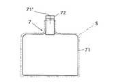
図4は電極の参考例の概略構成を示す図である。この電極7は前記図1のプラズマCVD装置における内部電極4に代えて用いることができるもので、ここでは導電性ゴムからなる袋状の電極71及び袋状電極71の開口部71’に挿入でき、開口部71’を塞ぐことができるだけの径を有するロッド形状の電極部材72からなる。成膜装置においては、電極部材72に電源が接続される。
【0056】
この電極7を図1のプラズマCVD装置における内部電極4に代えて用いて物品Sの外表面に膜形成するにあたっては、該袋状電極71を被成膜物品である中空物品S内に挿入した後、内部に空気を入れて該物品Sの内腔の略全体にわたり膨らませた状態で、電極部材72で栓をする。この状態で成膜を行う。なお、この場合被成膜物品Sは別途設けた支持部材により支持する。なお、電極部材72に空気等の導入管を接続するようにしてもよい。
【0057】
その他の動作は前記図1の装置を用いる場合と同様であり、中空物品Sの外表面に均一に又は略均一状に成膜できるという効果も同様である。
なお、ここでは導電性ゴムからなる袋状電極を用いたが、伸縮性を有しない導電性材料からなる袋状の電極であって折り畳んで物品S内部に挿入できるとともに、内部に空気等を入れることで物品Sの内腔の略全体にわたり膨らませることができるものを用いることもできる。また、袋状電極内部に入れる流動体は空気に限らず、気体、液体、物品Sの開口部S1を通すことができる大きさの固体粒子等のいずれであってもよい。また、袋状電極は導電性を有しないゴム等の袋の外表面に導電性膜を形成したもの又は導電性物質をコ−ティングしたものでも構わない。
【0058】
また、図5は本発明に係る電極のさらに他の例の概略構成を示す図である。この電極8は前記図1のプラズマCVD装置における内部電極4に代えて用いることができるもので、該物品Sの開口部S1を通すことができる大きさの導電性粒子81と物品Sの開口部S1から該物品S内部に挿入されるロッド形状の電極部材82からなる。
【0059】
この電極8を図1のプラズマCVD装置における内部電極4に代えて用いて物品Sの外表面に膜形成するにあたっては、袋状のシ−トsを物品S内へ挿入しておいてこの袋状シ−トs内に導電性粒子81を入れて物品Sの内腔に満たす。なお、シ−トsを用いず導電性粒子81を直接物品S内に入れてもよい。また、電極部材82を物品Sの開口部S1からその内部に挿入する。電源は電極部材82に接続される。この状態で成膜を行う。なお、この場合図1のプラズマCVD装置による場合と異なり、別途設けた支持部材上に中空物品Sを載置して成膜を行い、粒子81が物品Sからこぼれないようにする。
【0060】
その他の動作は前記図1の装置を用いる場合と同様であり、中空物品Sの外表面に均一に又は略均一状に成膜できるという効果も同様である。
なお、ここでは導電性粒子を用いているが、これに代えて水銀のような常温で液体の導電性金属又は粘度の高い液体に導電性の粉を懸濁したもの等の導電性流体を用いてもよい。
【0061】
また、図6は本発明にかかるプラズマCVD装置の他の例の概略構成を示す図である。この装置は、図1の装置において、高周波電源23に任意波形発生装置24が接続されたものである。その他の構成は図1の装置と同様であり、実質上同じ部品には同じ参照符号を付してある。
この装置を用いて被成膜物品Sの外表面に膜形成するにあたっては、高周波電源23及び任意波形発生装置24により形成したパルス変調高周波電力をマッチングボックス22を介して内部電極4に供給することにより成膜原料ガスをプラズマ化する。
【0062】
該パルス変調高周波電力は、13.56MHz以上の所定周波数の基本高周波電力に該所定周波数の1万分の1以上10分の1以下の範囲の変調周波数で変調を施した状態のものとする。また、デューティ比(オン時間/オン時間+オフ時間)は50%とする。その他の動作は、図1の装置を用いた成膜と同様である。
図6の装置及びこの装置を用いた成膜によると、成膜原料ガスのプラズマ化のために供給する電力をこのようなパルス変調を施した高周波電力とすることにより、高密度のプラズマが得られ、これにより反応率が向上し、低温で成膜できる。また、このような変調を施すことにより、物品表面での反応が進み、膜密着性を向上させることができるとともに成膜速度を向上させることができる。
【0063】
なお、このようにパルス変調高周波電力を用いるときも、図2〜図5に示す内部電極を利用できる。
次に、前記図1及び図6のプラズマCVD装置並びにこれらの装置の内部電極構造等に若干の変更を加えた装置を用いて、ポリエチレンテレフタレ−トからなる中空の被成膜物品の外表面にDLC膜を形成した実施例について説明する。
実施例1(図1の装置)
中空物品 材質 ポリエチレンテレフタレ−ト
形状 円筒状本体(直径100mm×高さ80mm、厚み0.1mm)
円筒状開口部(直径40mm×高さ20mm、厚み0.1mm)
電極 材質 ステンレススチ−ル
形状 中心部材(直径10mm×高さ120mm)
開き状態での最大径90mm
成膜条件
成膜用原料ガス 水素(H2) 20sccm
メタン(CH4) 20sccm
高周波電力 周波数13.56MHz、100W
成膜圧力 0.1Torr
成膜温度 室温
成膜時間 60min
実施例2(図1の装置において電極4に代えて図3の電極6を備えた装置)
中空物品 実施例1と同様
電極 材質 中心部材61 ステンレススチール SUS304
開閉部材62 Ti−Ni系合金、Cu−Zn−Al系合金
又はCu−Al−Ni系合金
形状 中心部材61(直径10mm×高さ120mm)
開閉部材62(高さ略80mm)
開き状態での最大径90mm
成膜条件
実施例1と同様
実施例3(図1の装置において電極4に代えて図5の電極8を備え、導電性粒子81に代 えて導電性流体を備えた装置)
中空物品 実施例1と同様
電極 材質 電極部材82 ステンレススチール SUS304
導電性流体 水銀
形状 電極部材82(直径5mm)
成膜条件
実施例1と同様
実施例4(図1の装置において電極4に代えて図5の電極8を備えた装置)
中空物品 実施例1と同様
電極 材質 電極部材82 ステンレススチール SUS304
導電性流動物81 ステンレススチール SUS304
形状 電極部材82(直径5mm)
導電性流動物81(直径5mmの球状粒子)
成膜条件
実施例1と同様
実施例5(参考例)(図1の装置において電極4に代えて図4の電極7を備えた装置)
中空物品 実施例1と同様
電極 材質 電極部材72 ステンレススチール SUS304
袋状電極71 カーボンブラックを配合した導電性ゴム又はシリコー ンゴム若しくはEPDMからなる袋表面にイオン蒸着 薄膜形成(IVD)法でCu、Ni若しくはAgから なる膜を形成したもの
電極部材72は、袋状電極内部へ空気を入れて袋を膨張させ、袋状電極71 の入口部分を内側へ折り返して導電性膜に接するように挿着した。
成膜条件
実施例1と同様
実施例6(図1の装置において電極4に代えて図5の電極8を備えた装置)
前記実施例4において、成膜原料ガスとしてメタン(CH4)(20sccm)及びヘキサフルオロエタン(C2F6)(20sccm)を用いた他は、実施例4と同様にして物品Sの外表面にDLC膜を形成した。
実施例7(図6の装置において電極4に代えて図5の電極8を備えた装置)
前記実施例4において、ガスプラズマ化用高周波電力として、周波数13.56MHz(100W)の基本高周波電力に変調周波数1kHz、デュ−ティ比50%でパルス変調を施した状態の高周波電力を用いた他は、実施例4と同様にして物品Sの外表面にDLC膜を形成した。
実施例8(図6の装置において電極4に代えて図5の電極8を備えた装置)
前記実施例4において、ガスプラズマ化用高周波電力として、周波数13.56MHz(100W)の基本高周波電力に変調周波数1kHz、デュ−ティ比50%でパルス変調を施した高周波電力を用い、また成膜原料ガスとしてメタン(CH4)(20sccm)及びヘキサフルオロエタン(C2F6)(20sccm)を用いた他は、実施例4と同様にして物品Sの外表面にDLC膜を形成した。
【0064】
すなわち、実施例8では、前記実施例6において、ガスプラズマ化用高周波電力として、周波数13.56MHz(100W)の基本高周波電力に変調周波数1kHz、デュ−ティ比50%でパルス変調を施した高周波電力を用いた他は、実施例6と同様にして物品Sの外表面にDLC膜を形成した。さらに換言すれば、前記実施例7において、成膜原料ガスとしてメタン(CH4)(20sccm)及びヘキサフルオロエタン(C2F6)(20sccm)を用いた他は、実施例7と同様にして物品Sの外表面にDLC膜を形成した。
比較例(図9の装置)
直径35mm、高さ120mmのステンレススチ−ルからなるロッド形状の内部電極21を備えた図9のプラズマCVD装置を用いて、前記実施例1と同じ成膜条件で同じ中空物品Sの外表面にDLC膜を形成しようとしたところ、膜形成は不可能であった。
【0065】
この結果、本発明の電極を備えたプラズマCVD装置を用いることにより、開口部の径に比して本体の径が大きい電気絶縁性材料からなる中空物品の外表面への成膜が可能になったことが分かる。
次に、前記実施例1〜6により得られた各DLC膜被覆物品及び前記比較例の操作を終えた物品について、それぞれ膜厚均一性、膜密着性、硬度、ガスバリア性を評価した。また、前記各例について成膜速度も算出した。また、前記実施例4、6、7及び8により得られた各DLC膜被覆物品について潤滑性を評価した。
【0066】
膜厚均一性は、被成膜物品の本体部分の高さ方向の両端から10mmづつ内側に入った各点の間を5等分した4点での膜厚を段差計を用いて測定し、そのばらつきを求めることで評価した。膜密着性は、前記各例と同条件で直径4インチのシリコンウエハに成膜したものについて成膜前後の撓みをレ−ザ変位計を用いて測定することで膜応力を測定し、膜応力が小さいほど密着性が良いとして評価した。硬度は0.5gヌ−プ硬度を測定することで評価した。ガスバリア性はMocon社製ガス透過測定装置を用い、25℃の温度下で、膜被覆中空物品の内側の酸素濃度を100%とし外側の酸素濃度を0%として酸素の透過速度を測定することで評価した。潤滑性は、膜又は物品表面に先端曲率R18mmのアルミニウムからなるピン状物品の先端部を当接させ、且つ、該ピン状物品に10gの荷重をかけた状態でこのピンを20mm/secの速度で移動させたときの値を測定した。結果を次の表1及び表2に示す。
【0067】
また表2の結果、実施例4において成膜原料ガスとして炭化水素化合物ガスに加えてフッ化炭素化合物ガスを用いた実施例6によるDLC膜被覆物品ではアルミニウム材との摩擦係数が減少し、潤滑性が向上したことが分かる。また、実施例4においてガスプラズマ化用高周波電力としてパルス変調高周波電力を用いた実施例7によるDLC膜被覆物品でも潤滑性が向上したことが分かる。さらに、実施例4において成膜原料ガスとして炭化水素化合物ガスに加えてフッ化炭素化合物ガスを用いるとともに、ガスプラズマ化用高周波電力としてパルス変調高周波電力を用いた実施例8によるDLC膜被覆物品では実施例6、7による物品よりさらに潤滑性が向上したことが分かる。
【0068】
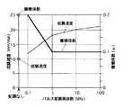
次に、図1の装置において電極4に代えて図5の電極8を備えた装置を用いたDLC膜形成において、ガスプラズマ化用電力として周波数13.56MHzの基本高周波電力に0.1kHz〜100kHz(基本高周波電力の周波数の約10万分の1〜100分の1)の範囲の変調周波数でパルス変調を施した状態の高周波電力を用い、変調周波数の変化に伴う成膜速度及びアルミニウム材との摩擦係数の変化を検討した。結果を図7に示す。
【0069】
この結果、前記変調周波数の範囲では変調周波数を高くするほど成膜速度が向上したことが分かる。なお、変調を施さない場合の成膜速度は10nm/minであり、変調周波数を1kHz(基本高周波電力の周波数の約1万分の1)程度以上とすることが好ましいことが分かる。
また、アルミニウム材との摩擦係数については、変調を施さない場合が0.2であるのに対して変調周波数1kHz〜100kHz(基本高周波電力の周波数の約1万分の1〜100分の1)で0.1となり、摩擦係数が低下し、潤滑性が向上したことが分かる。なお、変調周波数0.1kHz(基本高周波電力の周波数の約10万分の1)では摩擦係数は0.2であり、向上しなかったことが分かる。
【0070】
次に、実施例6において、成膜原料ガス中のヘキサフルオロエタンの混合比率(C2F6/CH4+C2F6)(重量比)を0〜1の範囲で変化させて成膜を行い、成膜速度を測定した。結果を図8に示す。この結果、メタンガスのみの場合に比べてヘキサフルオロエタンを混合することによりその混合比率が80%以下の範囲で成膜速度が向上したことが分かる。また、これ以上ヘキサフルオロエタンの混合比率を高くすると却って成膜速度が低下したことも分かる。
【0071】
【発明の効果】
以上のように本発明によると、開口部を有する中空物品の外表面に成膜するプラズマCVD法、プラズマCVD装置並びにかかる方法及び装置に用いることができる電極であって、該物品の形状にかかわらずその外表面に均一に又は略均一状に成膜できるプラズマCVD法、プラズマCVD装置並びにかかる方法及び装置に用いることができる電極をそれぞれ提供することができる。
【0072】
また、本発明によると、開口部を有する中空物品の外表面に成膜するプラズマCVD法、プラズマCVD装置並びにかかる方法及び装置に用いることができる電極であって、生産性良く成膜できるプラズマCVD法、プラズマCVD装置並びにかかる方法及び装置に用いることができる電極をそれぞれ提供することができる。
【図面の簡単な説明】
【図1】本発明に係るプラズマCVD装置の1例の概略構成を示す図である。
【図2】本発明に係る電極の他の例の概略構成を示す図である。
【図3】本発明に係る電極のさらに他の例の概略構成を示す図である。
【図4】電極の参考例の概略構成を示す図である。
【図5】本発明に係る電極のさらに他の例の概略構成を示す図である。
【図6】本発明に係るプラズマCVD装置の他の例の概略構成を示す図である。
【図7】本発明方法におけるガスプラズマ化用のパルス変調高周波電力の変調周波数と成膜速度の関係の1例及び該変調周波数とアルミニウム材との摩擦係数との関係の1例のそれぞれを示す図である。
【図8】本発明方法により炭素膜を形成する場合の成膜原料ガス中のフッ化炭素ガスの混合比率と成膜速度との関係の1例を示す図である。
【図9】中空物品の外表面に成膜できる従来のプラズマCVD装置の例の概略構成を示す図である。
【符号の説明】
1 真空チャンバ
11 排気装置
21 内部電極
21’ 支持部材
22 マッチングボックス
23 高周波電源
24 任意波形発生装置
3 成膜原料ガス供給部
4、5、6、7、8 内部電極
41 中心部材
42、42’ 開閉部材
43、43’ リング部材
44、44’、47 連結部材
45 駆動部材
46、46’ 固定部材
48 ストッパ装置
51 外筒体
51a スリット
52 中心軸棒
53 シ−ト状電極部材
61 中心部材
62 開閉部材
63 温度制御用流体通路
71 袋状電極
71’ 開口部
72 電極部材
81 導電性粒子
82 電極部材
s 袋状シ−ト
S 中空物品(被成膜物品)
S1 物品Sの外表面[0001]
BACKGROUND OF THE INVENTION
The present invention relates to a plasma CVD method for forming a film on the outer surface of a hollow article having an opening, a plasma CVD apparatus and an electrode that can be used in this method.
[0002]
[Prior art]
Resin is frequently used as a material for containers used in the food and pharmaceutical fields. Resin products have advantages such as light weight, excellent impact resistance, and low cost. However, since the resin container has poor gas barrier properties, the contents are oxidized, and a gas such as carbon dioxide gas contained in the contents is easily released to the outside. Moreover, since it is relatively soft, it is easily damaged by contact with other articles.
[0003]
Therefore, in recent years, attempts have been made to form a hard carbon film on the surface of a resin container, paying attention to the excellent wear resistance and gas barrier properties of a hard carbon film such as a DLC film.
For example, according to Japanese Patent Application Laid-Open No. 8-53117, a container to be formed with a film is installed in a hollow external electrode that is substantially similar to the outer shape of the container and has a space that is slightly larger than the container. A thin rod-like internal electrode that can be inserted from the mouth of the gas is inserted and installed, and the film forming raw material gas is introduced into the container using the internal electrode as a gas nozzle, and gas plasma is formed between the electrodes. A method and apparatus for forming a carbon film on the inner surface of the container by supplying high-frequency power is disclosed. In addition, when this method and apparatus are used, a negative self-bias is generated in the external electrode along the outer surface of the container, and a uniform film can be formed on the inner surface of the container. In addition, since the discharge region is narrow, exhaust can be efficiently performed and the film forming raw material gas can be reduced, so that the productivity is good.
[0004]
Further, as an apparatus for forming a film such as a carbon film on the outer surface of a container-shaped article to be deposited, a plasma CVD apparatus as shown in FIG. 9 is used. This apparatus has a
[0005]
When forming a film on the outer surface of a container-shaped film-formed article S, that is, a hollow article S having an opening using this apparatus, the film-formed article S is carried into the
[0006]
[Problems to be solved by the invention]
However, according to the plasma CVD method and apparatus taught by JP-A-8-53117, a carbon film is formed on the inner surface of the container, so that the effect of preventing damage due to contact with other articles cannot be obtained.
In addition, the figure9In the film formation using the plasma CVD apparatus, since the internal electrode to which high-frequency power is supplied is a rod-like one that is thinner than the inner diameter of the opening of the article to be deposited, the inner electrode is surrounded by the article wall. Depending on the shape of the article to be deposited, the formed plasma sheath does not follow the shape of the outer surface, and it may be difficult to form a film uniformly on the outer surface. In addition, since discharge is generated in the entire vacuum chamber, exhaust efficiency is poor and a large amount of film forming source gas is required, and thus, there is a problem that productivity is poor.
[0007]
Accordingly, the present invention provides a plasma CVD method, a plasma CVD apparatus, and an electrode that can be used in such a method and apparatus for forming a film on the outer surface of a hollow article having an opening, and the electrode can be used regardless of the shape of the article. It is an object of the present invention to provide a plasma CVD method, a plasma CVD apparatus, and an electrode that can be used in such a method and apparatus, which can form a film uniformly or substantially uniformly on the surface.
[0008]
The present invention also relates to a plasma CVD method for forming a film on the outer surface of a hollow article having an opening, a plasma CVD apparatus, and an electrode that can be used in such a method and apparatus. It is another object of the present invention to provide a plasma CVD apparatus and electrodes that can be used in such a method and apparatus.
[0009]
[Means for Solving the Problems]
In order to solve the above problems, the present invention is a plasma CVD method in which power is supplied to a film forming raw material gas to convert the gas into plasma, and a film is formed on the outer surface of a hollow article having an opening under the plasma. And using an internal electrode arranged in the lumen of the hollow article and an external electrode arranged outside as the electrode for supplying the gas plasma power, and passing the opening of the hollow article as the internal electrode Can be selectively used in accordance with the reduced shape or the volume and shape of the lumen of the article, and the inner electrode is formed in the reduced shape when forming the film on the outer surface of the article. The gas plasma power is supplied between the internal electrode and the external electrode in a state where the internal electrode is installed in the article as the enlarged shape after being inserted into the article lumen through the opening of the article. It is deposited on the outer surface of the article TeRupuA plasma CVD method is provided (first plasma CVD method of the present invention).
[0010]
In order to solve the above problems, the present invention provides a plasma CVD method in which power is supplied to a film forming source gas to turn the gas into plasma, and a film is formed on the outer surface of a hollow article having an opening under the plasma. The device includes an internal electrode disposed in a lumen of the hollow article and an external electrode disposed outside as an electrode for supplying the gas plasma power, and the internal electrode is an opening of the hollow article. Can be selectively taken in a reduced shape that can be passed through, or a predetermined enlarged shape depending on the volume and shape of the lumen of the articleRupuA plasma CVD apparatus is provided (first plasma CVD apparatus of the present invention).
[0011]
In order to solve the above problems, the present invention provides a plasma CVD method in which power is supplied to a film forming source gas to turn the gas into plasma, and a film is formed on the outer surface of a hollow article having an opening under the plasma. The internal electrode is disposed in the lumen of the hollow article and is supplied with the gas plasma power from an external electrode arranged outside the hollow article, and passes through the opening of the article. Can be selectively taken in a reduced shape or a predetermined enlarged shape according to the volume and shape of the lumen of the article.RudenA pole is provided (first electrode of the present invention).
[0012]
According to the first plasma CVD method, the plasma CVD apparatus, and the electrode of the present invention, the electrode disposed in the lumen of the hollow article to be deposited is enlarged so as to correspond to the volume and shape of the article lumen. By setting, a plasma sheath can be formed in a region along or substantially along the outer surface of the article, and a film can be formed uniformly or substantially uniformly on the surface.
[0013]
This also reduces the internal electrode's reduced and enlarged shapes for hollow articles having a relatively large body lumen diameter compared to the inner diameter of the opening, and irregularly shaped hollow articles having a curved shape. By making it possible to set according to the shape of the article, a film can be formed uniformly or substantially uniformly on the outer surface of the article.
The hollow article as the film-formed article in the present invention may be a hollow article having at least one opening, but the outer surface of the article is placed in a plasma sheath formed along the internal electrode. It is possible to target articles that are thick enough to be able to.
[0014]
The internal electrode in the first electrode of the present invention and the first plasma CVD apparatus of the present invention can be opened and closed, for example, and can be set to the reduced shape by being closed and opened. It can be set to the enlarged shape.
Similarly, in the first method of the present invention, for example, an internal electrode that can be opened and closed is used, and when the film is formed on the article, the internal electrode is closed to form the reduced shape. After being inserted into the article lumen from the opening of the article, it is set in the article as the enlarged shape by opening it, and the gas plasma power is supplied between the internal electrode and the external electrode. A film can be formed on the outer surface of the article.
[0015]
The openable / closable internal electrode includes a center member, an openable / closable member connected to the openable / closable member, and a drive unit for opening / closing the openable / closable member. The thing which can be set to can be illustrated.
Furthermore, as such an internal electrode, (1) an electrode that can be opened and closed like an umbrella bone, (2) a flexible sheet-like electrode member is opened by being drawn out along the inner wall surface of the article lumen, and is closed by being wound up. The thing etc. can be illustrated.
[0016]
Regarding the internal electrode that can be opened and closed in the shape of an umbrella in (1), as a more specific example, a plurality of opening and closing members are arranged around the rod-shaped center member at predetermined center angle intervals, and one end of each opening and closing member is connected to the center member. A drive member for pivotally connecting to a predetermined part and having the other end slidably connected to a ring member slidably fitted to the central member and sliding the ring member on the central member. And the opening member can be closed and set to the reduced shape by sliding the ring member with the driving member, and the internal electrode can be set to the enlarged shape by opening the opening and closing member. . In this case, the plurality of opening / closing member groups and the ring member connected thereto may be provided in a plurality of stages on the central member. Moreover, you may provide the stopper apparatus which connects the said drive member so that it cannot move to a center member in the state set to the reduction | decrease shape or the expansion shape as a whole.
[0017]
As a further specific example of the internal electrode employing the flexible sheet-like electrode member according to (2), an outer cylinder that can pass through the article opening, and a central shaft bar that is rotatably supported in the outer cylinder (Central member) and a flexible sheet-like electrode member that is connected to the shaft rod at one end and can move in and out of the outer cylinder body through a slit formed in the outer cylinder body by a rotation operation of the shaft rod The sheet-like electrode member can be set to the reduced shape by winding the central axis rod by winding and turning operation, and the sheet-like electrode member can be set to the article by rotating and rotating the central axis rod. The internal electrode which can be set to the said enlarged shape by extending | stretching along the inner wall face of a lumen can be mentioned.
[0018]
Further, the first electrode of the present invention and the internal electrode in the first apparatus of the present invention are made of a shape memory alloy, set to the enlarged shape at a temperature taking a memory shape, and can be deformed at a lower temperature than that. It can be set at the reduced shape by being deformed at a suitable temperature.
Similarly, in the first method of the present invention, the internal electrode is made of a shape memory alloy, is set to the enlarged shape at a temperature that takes a memory shape, and is deformed at a temperature that can be deformed at a lower temperature. When the film can be formed on the film-formed article, the internal electrode is transformed into the reduced shape at the low temperature and inserted into the article lumen through the opening of the article. After that, the internal electrode is returned to the enlarged shape at a temperature that takes the memorized shape, and the gas plasma power is supplied between the internal electrode and the external electrode to form a film on the outer surface of the article. can do.
[0019]
As an electrode made of such a shape memory alloy, typically, an electrode which can take the enlarged shape in the parent phase state of the shape memory alloy and can be transformed into the reduced shape in the martensite phase state can be exemplified.
In any case, the internal electrode may be temperature-controlled during film formation and / or before film formation, particularly during film formation, in order to set the enlarged shape or reduced shape as necessary. For this purpose, a temperature control device for setting the enlarged shape and / or the reduced shape may be provided in the internal electrode. Such a temperature control device includes a heater and / or a cooler combined with an internal electrode, a device for circulating a temperature-controlled gas or liquid fluid in a fluid passage formed in the internal electrode, and enclosed in the internal electrode Examples thereof include a gas for controlling temperature, a liquid containing a liquid fluid, a combination of a heater and / or a cooler for controlling the temperature of the enclosed fluid, and an appropriate combination thereof.
[0020]
The shape memory alloy is not limited to this, but other than Ti—Ni alloy, Cu—Zn—Al alloy, Cu—Al—Ni alloy, Cu—Zn alloy, In—Tl alloy. A suitable material can be employed from among alloys, Ni-Al alloys, Fe-Pd alloys and the like. For example, it is desirable to use a material and a composition ratio that take a parent phase state at a film formation temperature (about 25 ° C. to 100 ° C.) in plasma CVD.
[0021]
The internal electrode isAt least the outer surface is a conductive bag-like electrode that can be inflated by putting a fluid inside and set to the enlarged shape, and can be set to the reduced shape by taking out the fluid from the inside. To doIs possible.
When using such a bag-like electrode,In forming the film on the article, the bag-like electrode is inserted into the article lumen from the article opening, and then a fluid is put into the bag-like electrode to inflate it to form the enlarged shape in the article. It is possible to form a film on the outer surface of the article by installing and supplying the gas plasma power between the internal electrode and the external electrode.
[0022]
Examples of the bag-like electrode include a stretchable conductive sheet (for example, a conductive rubber sheet) and a conductive sheet that is not stretchable and can be compressed by folding. The bag-like electrode may be conductive as a whole, or may have conductivity only on the outer surface (for example, a conductive film formed on the outer surface or coated with a conductive substance). Even so, at least the outer surface shall have conductivity.
[0023]
Examples of the conductive rubber include, but are not limited to, butadiene-styrene copolymer (SBR), polybutadiene (BR), ethylene-propylene-diene terpolymer (EPDM), silicone rubber, Examples thereof include those obtained by blending a conductive filler such as carbon black powder, graphite powder, metal powder, and metal fiber with rubber such as fluoro rubber, and polyacetylene that is structurally conductive.
[0024]
The fluid contained in the bag-like electrode may be a fluid such as liquid or gas, or may be composed of solid particles (particles smaller than the inner diameter of the opening of the hollow article).
In the case where the bag-like electrode is entirely conductive, when the power is to be supplied via the fluid placed in the lumen, the fluid may be a conductive fluid. As the conductive fluid, in addition to mercury that is liquid at room temperature, for example, a liquid in which conductive powder such as iron powder is suspended can be used. In this case, it is desirable to suspend the powder in a liquid having a viscosity as high as possible so that the powder does not easily precipitate during film formation. Moreover, the fluid which consists of electroconductive solids, such as electroconductive powder and electroconductive particle, can also be used.
[0025]
In order to solve the above problems, the present invention provides a plasma CVD method in which power is supplied to a film forming source gas to turn the gas into plasma, and a film is formed on the outer surface of a hollow article having an opening under the plasma. Using an internal electrode arranged in the lumen of the hollow article and an external electrode arranged outside as the electrode for supplying the gas plasma power, and through the opening of the hollow article as the internal electrode material Adopting a conductive fluid that can flow in and out of the article, and forming the inner electrode by forming the film on the outer surface of the article by flowing the conductive fluid into the article lumen from the article opening, A plasma CVD method is provided in which the gas plasma power is supplied between the internal electrode and the external electrode to form a film on the outer surface of the article (second plasma CVD method of the present invention). .
[0026]
In order to solve the above problems, the present invention provides a plasma CVD method in which power is supplied to a film forming source gas to turn the gas into plasma, and a film is formed on the outer surface of a hollow article having an opening under the plasma. The device includes an internal electrode disposed in a lumen of the hollow article and an external electrode disposed outside as an electrode for supplying the gas plasma power, and the internal electrode is an opening of the hollow article. A plasma CVD apparatus comprising a conductive fluid that can flow into and out of the article through the interior of the article, and that can flow into the lumen of the article and form on the internal electrode (second embodiment of the present invention) Plasma CVD apparatus).
[0027]
In order to solve the above problems, the present invention provides a plasma CVD method in which power is supplied to a film forming source gas to turn the gas into plasma, and a film is formed on the outer surface of a hollow article having an opening under the plasma. The internal electrode is disposed in the inner cavity of the hollow article and is supplied with the gas plasma power from an external electrode disposed outside the hollow article, and the article is opened through the opening of the article. An electrode is provided that includes a conductive fluid that can flow into and out of the body and can flow into the lumen of the article to form the internal electrode (second electrode of the present invention).
[0028]
According to the second plasma CVD method and apparatus of the present invention, the conductive electrode is made to flow into the lumen of the hollow article to form the internal electrode in a state where the lumen is filled or substantially filled, A plasma sheath can be formed in a region along or substantially along the outer surface of the article, and a film can be formed uniformly or substantially uniformly on the surface.
[0029]
As such a conductive fluid, solid particles made of a conductive material such as iron, stainless steel, and aluminum (particles in the form of granules, powders, flakes, etc.) having a diameter smaller than the inner diameter of the opening of the hollow article, Examples include conductive fluids such as conductive liquids and combinations thereof.
As the conductive fluid, it is possible to use a liquid in which conductive powder such as mercury or iron powder that is liquid at room temperature is suspended. In this case, it is desirable to suspend the powder in a liquid having a viscosity as high as possible so that the powder does not easily precipitate during film formation.
[0030]
In any case, in order to prevent the conductive fluid from adsorbing to the inner wall surface of the hollow article, a sheet made of a synthetic resin or the like is interposed between the inner wall surface and the fluid flows into the article. You may let them. Further, for example, a bag made of a synthetic resin film may be inserted into the article first, and the conductive electrode may be put into the bag to constitute the internal electrode.
[0031]
In supplying power to the conductive fluid that has flowed into the article lumen, an electrode member may be inserted into the conductive fluid through the opening of the article, and power may be supplied through the electrode member. .
In the first and second plasma CVD methods and apparatuses of the present invention, the external electrode may be the plasma generation chamber itself in which the hollow article is installed and the plasma is formed as an external electrode. It may be an electrode arranged outside the article.
[0032]
Further, either the internal electrode or the external electrode may be an electrode on the side connected to a power source for supplying gas plasma power, but usually the internal electrode is an electrode on the side connected to the power source. And the external electrode may be a ground electrode.
In the first and second plasma CVD methods and apparatuses according to the present invention, either high frequency power or direct current power can be used as the gas plasma power.
[0033]
In the first and second plasma CVD methods, when high-frequency power is used as the power for gas plasma generation, the power is converted into basic high-frequency power with a predetermined frequency of 13.56 MHz or more and 1 / 10,000 or more and 10 minutes of the predetermined frequency. In other words, the amplitude modulation can be performed at a modulation frequency in the range of 1 or less.
Further, in the first and second plasma CVD apparatuses, as a means for supplying gas plasma power between the internal electrode and the external electrode, the predetermined high frequency power of 13.56 MHz or higher is applied to the predetermined high frequency power. Can supply power in a state where amplitude modulation is performed at a modulation frequency in the range of 1 / 10,000 to 1/10.
[0034]
By making the electric power supplied for the plasma formation of the film forming raw material gas into such a modulated high frequency electric power, a high density plasma can be obtained, thereby improving the reaction rate and forming a film at a low temperature. Further, by performing such modulation, reaction on the outer surface of the hollow article that is the article to be deposited proceeds, so that the film adhesion can be improved and the film forming speed can be improved. Thereby, productivity can be improved. Further, when a carbon film is formed as described later, the lubricity of the film can be improved.
[0035]
The waveform of the basic high frequency power before modulation may be a sine wave, a rectangular wave, a sawtooth wave, a triangular wave, or the like. The amplitude modulation may be pulse modulation by turning on / off the power supply, and may be pulse-like modulation.
The reason why the basic high frequency power of 13.56 MHz or more is used is that the plasma density tends to be insufficient when the power is lower than this. Further, the frequency of the basic high-frequency power may be set to, for example, about 500 MHz from the viewpoint of the high-frequency power supply cost.
[0036]
Further, the reason why the modulation frequency within the above range is used is that the film formation rate is drastically decreased when the modulation frequency becomes smaller than 1 / 10,000 of the frequency of the basic high frequency power. This is because matching becomes difficult and the film thickness uniformity decreases as the size increases.
The pulse modulation duty ratio (on time / on time + off time) may be about 10% to 90%. This is because the film formation rate decreases when the ratio is smaller than 10%, and the power supply time becomes too long when the ratio is larger than 90%, and the effect of improving the plasma density by the modulated high-frequency power is reduced. .
[0037]
In the first and second plasma CVD methods and apparatuses, methane (CHFour), Ethane (C2H6), Propane (CThreeH8), Butane (CFourHTen), Acetylene (C2H2), Benzene (C6H6), Etc., and if necessary, these hydrocarbon compound gases mixed with hydrogen gas, inert gas, etc. as a carrier gas to form a carbon film on the outer surface of the hollow article Can do.
[0038]
As a film forming raw material gas in the case of forming a carbon film, it is desirable to use a gas obtained by mixing a gas of a fluorocarbon compound with a gas of the hydrocarbon compound. Tetrafluoromethane (CFFour) Gas, hexafluoroethane (C2F6) Gas, octafluorocyclobutane (CFourF8) Gas etc. can be mentioned. In forming the carbon film, the deposition rate can be improved by mixing the hydrocarbon compound gas with the fluorocarbon compound gas. Thereby, productivity can be improved. In addition, effects such as improvement in film adhesion, improvement in gas barrier properties, and improvement in lubricity due to reduction in film stress can be obtained.
[0039]
When a mixed gas of a hydrocarbon compound gas and a fluorocarbon compound gas is used as a film forming raw material gas, the mixture ratio of the fluorocarbon compound gas (fluorocarbon / (fluorocarbon + Hydrocarbon))) is preferably about 80% or less by weight. When the mixing ratio of the fluorocarbon compound gas exceeds 80% of the whole, the effect of improving the film forming speed is not obtained so much, and only the fluorocarbon compound gas is etched depending on the material of the film to be deposited. End up. The mixing ratio of the fluorocarbon compound gas is more preferably about 20% to 70% by weight.
[0040]
A typical example of the carbon film is a DLC (Diamond Like Carbon) film. The DLC film has good lubricity, is not easily worn by friction with other articles, and the article to be deposited has flexibility by adjusting its thickness. It is a carbon film having an appropriate hardness that can be reduced to such an extent that the original flexibility is not impaired. Further, the gas barrier property is good. Further, since light can be transmitted by adjusting the thickness thereof, the contents can be seen even if formed on the surface of a hollow article, which is suitable as a film formed on a hollow article for container purposes. Furthermore, the film can be formed easily, such as being formed at a relatively low temperature.
[0041]
In the plasma CVD method, when a carbon compound gas is used as a film forming source gas, a film forming pressure is set to about 100 mTorr, and a film forming temperature is set to 100 ° C. or less, a DLC film is formed. The higher the film formation temperature, the higher the hardness of the formed film, and a carbon film having excellent wear resistance is formed at 500 ° C. or higher. Above 900 ° C., a diamond film is formed.
[0042]
In the first and second plasma CVD methods and apparatuses, a plurality of internal electrodes can be used to form a film on a plurality of hollow articles in one batch, thereby improving productivity. Can do.
There are no particular limitations on the material of the film-forming article to be deposited by the first and second plasma CVD methods, apparatuses, and electrodes of the present invention, but the article to be deposited is ceramic, glass, polymer material (resin, Even in the case of a hollow article made of an electrically insulating material such as rubber, a plasma sheath can be formed along or substantially along the outer surface of the article by using the electrode of the present invention. Thus, film formation can be performed uniformly or substantially uniformly on the outer surface of the article.
[0043]
When a hard carbon film such as a DLC film is formed, the film is formed on the outer surface of a hollow article made of a polymer material having a relatively low hardness and poor lubricity and gas barrier properties. Surface wear resistance, lubricity, gas barrier properties, and the like can be improved.
Examples of the resin include the following thermoplastic resins. That is, vinyl resins (polyvinyl chloride, polyvinyl dichloride, polyvinyl butyrate, polyvinyl alcohol, polyvinyl acetate, polyvinyl formal, etc.), polyvinylidene chloride, chlorinated polyether, polyester resins (both polystyrene, styrene / acrylonitrile) Polymers, etc.), ABS, polyethylene, polypropylene, polyacetal, acrylic resins (polymethyl methacrylate, modified acrylics, etc.), polyamide resins (
[0044]
Examples of the resin also include the following thermosetting resins. That is, phenol / formaldehyde resin, urea resin, melamine / formaldehyde resin, epoxy resin, furan resin, xylene resin, unsaturated polyester resin, silicone resin, diallyl phthalate resin and the like.
Examples of the rubber include natural rubber, butyl rubber, ethylene propylene rubber, chloroprene rubber, chlorinated polyethylene rubber, epichlorohydrin rubber, acrylic rubber, nitrile rubber, urethane rubber, silicone rubber, and fluorine rubber.
[0045]
DETAILED DESCRIPTION OF THE INVENTION
Hereinafter, embodiments of the present invention will be described with reference to the drawings.
FIG. 1 is a diagram showing a schematic configuration of an example of a plasma CVD apparatus according to the present invention. This apparatus is provided with an umbrella-shaped
[0046]
The
Other configurations are the same as those of the apparatus shown in FIG. 9, and substantially the same components are denoted by the same reference numerals.
[0047]
In forming a film on the outer surface of the hollow article S using this apparatus, initially, the open /
[0048]
According to the film forming apparatus and method, since a plasma sheath can be formed in a region substantially along the outer surface of the hollow article S, a film can be formed uniformly or substantially uniformly on the surface. Moreover, FIG. 2 is a figure which shows schematic structure of the other example of the electrode which concerns on this invention. This
[0049]
When the
[0050]
Other operations are the same as in the case of using the apparatus shown in FIG. 1, and the effect that the film can be formed uniformly or substantially uniformly on the outer surface of the hollow article S is also the same.
FIG. 3 is a diagram showing a schematic configuration of still another example of the electrode according to the present invention. This electrode 6 can be used in place of the
[0051]
The opening / closing
[0052]
Further, here, a cooling or
[0053]
In the film forming apparatus, the high frequency power source is connected to the
When the electrode 6 is used in place of the
[0054]
In the case of using a shape memory alloy that becomes a parent phase at the temperature during plasma CVD without performing temperature control using a fluid, it is not necessary to perform temperature control during film formation.
Other operations are the same as in the case of using the apparatus shown in FIG. 1, and the effect that the film can be formed uniformly or substantially uniformly on the outer surface of the hollow article S is also the same.
[0055]
Figure 4 shows a reference example of the electrode.It is a figure which shows schematic structure. This
[0056]
When the
[0057]
Other operations are the same as in the case of using the apparatus shown in FIG. 1, and the effect that the film can be formed uniformly or substantially uniformly on the outer surface of the hollow article S is also the same.
Although a bag-like electrode made of conductive rubber is used here, it is a bag-like electrode made of a non-stretchable conductive material that can be folded and inserted into the article S, and air or the like is put inside the bag. Thus, it is possible to use one that can be inflated over substantially the entire lumen of the article S. Moreover, the fluid put into the bag-shaped electrode is not limited to air, and may be any of gas, liquid, solid particles having a size that allows the opening S1 of the article S to pass through. Further, the bag-like electrode may be a non-conductive rubber or the like formed by forming a conductive film on the outer surface of a bag or by coating a conductive substance.
[0058]
FIG. 5 is a diagram showing a schematic configuration of still another example of the electrode according to the present invention. The
[0059]
When the
[0060]
Other operations are the same as in the case of using the apparatus shown in FIG. 1, and the effect that the film can be formed uniformly or substantially uniformly on the outer surface of the hollow article S is also the same.
In addition, although conductive particles are used here, instead of this, use is made of a conductive fluid such as a conductive metal that is liquid at room temperature such as mercury or a liquid in which conductive powder is suspended in a liquid with high viscosity. May be.
[0061]
Moreover, FIG. 6 is a figure which shows schematic structure of the other example of the plasma CVD apparatus concerning this invention. In this apparatus, an
When forming a film on the outer surface of the film-formed article S using this apparatus, pulse modulated high-frequency power formed by the high-
[0062]
The pulse-modulated high-frequency power is in a state where basic high-frequency power having a predetermined frequency of 13.56 MHz or higher is modulated at a modulation frequency in the range of 1 / 10,000 to 1/10 of the predetermined frequency. The duty ratio (on time / on time + off time) is 50%. Other operations are the same as the film formation using the apparatus of FIG.
According to the apparatus of FIG. 6 and film formation using this apparatus, high-density plasma can be obtained by using high-frequency power subjected to such pulse modulation as the power to be supplied for forming the film forming material gas into plasma. As a result, the reaction rate is improved and the film can be formed at a low temperature. Further, by performing such modulation, the reaction on the surface of the article proceeds, so that film adhesion can be improved and the film formation rate can be improved.
[0063]
Note that the internal electrodes shown in FIGS. 2 to 5 can also be used when pulse-modulated high-frequency power is used.
Next, the outer surface of a hollow film-formed article made of polyethylene terephthalate using the plasma CVD apparatus of FIGS. 1 and 6 and an apparatus in which the internal electrode structure of these apparatuses is slightly changed. An embodiment in which a DLC film is formed will be described.
Example 1 (apparatus of FIG. 1)
Hollow article Material Polyethylene terephthalate
Shape Cylindrical body (diameter 100mm x height 80mm, thickness 0.1mm)
Cylindrical opening (diameter 40mm x height 20mm, thickness 0.1mm)
Electrode material Stainless steel
Shape Central member (diameter 10mm x height 120mm)
Maximum diameter 90mm in open state
Deposition conditions
Deposition source gas Hydrogen (H220sccm
Methane (CHFour20sccm
High frequency power frequency 13.56MHz, 100W
Deposition pressure 0.1 Torr
Deposition temperature Room temperature
Deposition time 60min
Example 2 (device provided with the electrode 6 of FIG. 3 instead of the
Hollow article Same as Example 1
Electrode
Opening / closing
Or Cu-Al-Ni alloy
Shape Center member 61 (diameter 10mm x height 120mm)
Opening / closing member 62 (height approximately 80mm)
Maximum diameter 90mm in open state
Deposition conditions
Same as Example 1
Example 3 (the apparatus having the
Hollow article Same as Example 1
Electrode
Conductive fluid Mercury
Shape Electrode member 82 (diameter 5mm)
Deposition conditions
Same as Example 1
Example 4 (device provided with the
Hollow article Same as Example 1
Electrode
Shape Electrode member 82 (diameter 5mm)
Conductive fluid 81 (spherical particles with a diameter of 5 mm)
Deposition conditions
Same as Example 1
Example 5(Reference example)(Device provided with
Hollow article Same as Example 1
Electrode
Bag-shaped electrode 71 A film made of Cu, Ni, or Ag formed by ion deposition thin film formation (IVD) method on the bag surface made of conductive rubber, silicon rubber, or EPDM mixed with carbon black
The
Deposition conditions
Same as Example 1
Example 6 (device provided with
In Example 4, methane (CHFour) (20 sccm) and hexafluoroethane (C2F6) (20 sccm) was used, and a DLC film was formed on the outer surface of the article S in the same manner as in Example 4.
Example 7 (device provided with the
In the fourth embodiment, the high frequency power for gas plasma is obtained by using the high frequency power in a state where pulse modulation is performed with a modulation frequency of 1 kHz and a duty ratio of 50% on the basic high frequency power with a frequency of 13.56 MHz (100 W). In the same manner as in Example 4, a DLC film was formed on the outer surface of the article S.
Example 8 (device provided with
In Example 4, high-frequency power obtained by applying pulse modulation with a modulation frequency of 1 kHz and a duty ratio of 50% to basic high-frequency power with a frequency of 13.56 MHz (100 W) is used as the high-frequency power for gas plasma. Methane (CHFour) (20 sccm) and hexafluoroethane (C2F6) (20 sccm) was used, and a DLC film was formed on the outer surface of the article S in the same manner as in Example 4.
[0064]
That is,In Example 8,In Example 6, the high frequency power for gas plasma was used except that the basic high frequency power with a frequency of 13.56 MHz (100 W) was subjected to pulse modulation with a modulation frequency of 1 kHz and a duty ratio of 50%. A DLC film was formed on the outer surface of the article S in the same manner as in Example 6. In other words, in Example 7, methane (CHFour) (20 sccm) andHexafluoroethane (C2F6)A DLC film was formed on the outer surface of the article S in the same manner as in Example 7 except that (20 sccm) was used.
Comparative example (apparatus of FIG. 9)
On the outer surface of the same hollow article S under the same film forming conditions as in Example 1, using the plasma CVD apparatus of FIG. 9 provided with a rod-shaped
[0065]
As a result, by using the plasma CVD apparatus provided with the electrode of the present invention, it becomes possible to form a film on the outer surface of a hollow article made of an electrically insulating material having a main body diameter larger than the opening diameter. I understand that.
Next, the film thickness uniformity, film adhesion, hardness, and gas barrier property were evaluated for each DLC film-coated article obtained in Examples 1 to 6 and the article after the operation of the comparative example was completed. In addition, the film formation rate was also calculated for each of the above examples. Further, the lubricity of each DLC film-coated article obtained in Examples 4, 6, 7, and 8 was evaluated.
[0066]
The film thickness uniformity was measured using a step meter to measure the film thickness at four points, which were divided into five equal parts between each point that entered inside 10 mm from both ends in the height direction of the body part of the film-formed article, It evaluated by calculating | requiring the dispersion | variation. For film adhesion, film stress was measured by measuring deflection before and after film formation on a silicon wafer having a diameter of 4 inches under the same conditions as in the above examples using a laser displacement meter. The smaller the value, the better the adhesion. Hardness was evaluated by measuring 0.5 g Knoop hardness. The gas barrier property is measured by measuring the permeation rate of oxygen at a temperature of 25 ° C. by using a gas permeation measuring device manufactured by Mocon, with the inner oxygen concentration of the membrane-coated hollow article being 100% and the outer oxygen concentration being 0%. evaluated. The lubricity is such that the tip of a pin-shaped article made of aluminum having a tip curvature R of 18 mm is brought into contact with the surface of the film or article, and the pin is moved at a speed of 20 mm / sec with a load of 10 g applied to the pin-shaped article. The value when moved by was measured. The results are shown in the following Tables 1 and 2.
[0067]
Further, as a result of Table 2, in the DLC film-coated article according to Example 6 using the fluorocarbon compound gas in addition to the hydrocarbon compound gas as the film forming raw material gas in Example 4, the friction coefficient with the aluminum material is reduced and lubrication is performed. It can be seen that the property has improved. Moreover, it turns out that lubricity improved also in the DLC film coating article by Example 7 which used pulse modulation high frequency electric power as high frequency electric power for gas plasma formation in Example 4. FIG. Furthermore, in Example 4, the fluorocarbon compound gas is used as the film forming raw material gas in addition to the hydrocarbon compound gas, and the DLC film-coated article according to Example 8 that uses pulse-modulated high-frequency power as the high-frequency power for gas plasma conversion is used. It can be seen that the lubricity was further improved compared to the articles according to Examples 6 and 7.
[0068]
Next, in the DLC film formation using the apparatus provided with the
[0069]
As a result, it can be seen that in the range of the modulation frequency, the film formation rate is improved as the modulation frequency is increased. In addition, it turns out that the film-forming speed | rate in the case of not modulating is 10 nm / min, and it is preferable to make a modulation frequency about 1 kHz (about 1 / 10,000 of the frequency of fundamental high frequency electric power) or more.
The coefficient of friction with the aluminum material is 0.2 when no modulation is applied, whereas the modulation frequency is 1 kHz to 100 kHz (about 1 / 10,000 to 1/100 of the frequency of the basic high-frequency power). It becomes 0.1, and it turns out that a friction coefficient fell and lubricity improved. It can be seen that at a modulation frequency of 0.1 kHz (about 1 / 100,000 of the frequency of the basic high-frequency power), the friction coefficient was 0.2, which was not improved.
[0070]
Next, in Example 6, the film-forming source gas containsHexafluoroethaneMixing ratio (C2F6/ CHFour+ C2F6) (Weight ratio) was changed in the range of 0 to 1 to form a film, and the film formation rate was measured. The results are shown in FIG. As a result, compared to methane gas aloneHexafluoroethaneIt can be seen that the film formation rate was improved when the mixing ratio was 80% or less. Also no moreHexafluoroethaneIt can also be seen that when the mixing ratio is increased, the film forming speed is decreased.
[0071]
【The invention's effect】
As described above, according to the present invention, a plasma CVD method, a plasma CVD apparatus, and an electrode that can be used in such a method and apparatus for forming a film on the outer surface of a hollow article having an opening, are used regardless of the shape of the article. It is possible to provide a plasma CVD method, a plasma CVD apparatus, and an electrode that can be used in such a method and apparatus, respectively, which can form a film uniformly or substantially uniformly on the outer surface thereof.
[0072]
In addition, according to the present invention, a plasma CVD method for forming a film on the outer surface of a hollow article having an opening, a plasma CVD apparatus, and an electrode that can be used in such a method and apparatus, which can be formed with high productivity. And plasma CVD apparatus and electrodes that can be used in such a method and apparatus can be provided.
[Brief description of the drawings]
FIG. 1 is a diagram showing a schematic configuration of an example of a plasma CVD apparatus according to the present invention.
FIG. 2 is a diagram showing a schematic configuration of another example of an electrode according to the present invention.
FIG. 3 is a diagram showing a schematic configuration of still another example of an electrode according to the present invention.
[Fig. 4]Reference example of electrodeIt is a figure which shows schematic structure.
FIG. 5 is a diagram showing a schematic configuration of still another example of an electrode according to the present invention.
FIG. 6 is a diagram showing a schematic configuration of another example of a plasma CVD apparatus according to the present invention.
FIG. 7 shows an example of the relationship between the modulation frequency of the pulse-modulated high-frequency power for gas plasma generation and the film forming speed in the method of the present invention, and an example of the relationship between the modulation frequency and the friction coefficient of the aluminum material. FIG.
FIG. 8 is a graph showing an example of the relationship between the mixing ratio of the fluorocarbon gas in the film forming raw material gas and the film forming speed when forming a carbon film by the method of the present invention.
FIG. 9 is a diagram showing a schematic configuration of an example of a conventional plasma CVD apparatus capable of forming a film on the outer surface of a hollow article.
[Explanation of symbols]
1 Vacuum chamber
11 Exhaust device
21 Internal electrode
21 'support member
22 Matching box
23 High frequency power supply
24 Arbitrary waveform generator
3 Deposition source gas supply unit
4, 5, 6, 7, 8 Internal electrode
41 Center member
42, 42 'opening and closing member
43, 43 'ring member
44, 44 ', 47 Connecting member
45 Drive member
46, 46 'fixing member
48 Stopper device
51 outer cylinder
51a slit
52 Center axis rod
53 Sheet Electrode Member
61 Center member
62 Opening / closing member
63 Fluid path for temperature control
71 Bag-shaped electrode
71 'opening
72 Electrode member
81 conductive particles
82 Electrode member
s Bag-shaped sheet
S Hollow article (deposition article)
S1 External surface of article S
Claims (21)
Translated fromJapanese前記内部電極として、ロッド形状の中心部材と、該中心部材の周囲に所定中心角度間隔で配置された複数個の開閉部材と、該中心部材に摺動可能に嵌められたリング部材と、該リング部材を中心部材に沿って摺動させるための駆動部材とを含み、各開閉部材を、該リング部材の該中心部材に沿う摺動により傘状に開閉するように該中心部材と該リング部材に連結した電極を用い、前記物品外表面への成膜にあたっては、該駆動部材で該リング部材を摺動させることで該開閉部材を閉じて前記縮小形状として該物品の開口部を通して該物品内腔に挿入した後、該駆動部材で該開閉部材を開くことで前記拡大形状に設定して該物品内に設置することを特徴とするプラズマCVD法。This is a plasma CVD method in which power is supplied to a film forming raw material gas to convert the gas into plasma, and a film is formed on the outer surface of a hollow article having an opening under the plasma, and the power for gas plasma conversion is supplied. An internal electrode arranged in the lumen of the hollow article and an external electrode arranged outside are used as electrodes, and the internal electrode has a reduced shape capable of passing through the opening of the hollow article or the lumen of the article Using an article that can selectively take a predetermined enlarged shape according to the volume and shape, and forming the inner electrode as the reduced shape when forming the film on the outer surface of the article, the article lumen through the opening of the article After being inserted into the article, the internal electrode is installed in the article in the enlarged shape, and the gas plasma power is supplied between the internal electrode and the external electrode to form a film on the outer surface of the article. ,
As the internal electrode, a rod-shaped central member, a plurality of opening / closing members disposed at predetermined central angular intervals around the central member, a ring member slidably fitted to the central member, and the ring A drive member for sliding the member along the center member, and the center member and the ring member are opened and closed in an umbrella shape by sliding along the center member of the ring member. When forming a film on the outer surface of the article using a connected electrode, the opening and closing member is closed by sliding the ring member with the driving member to form the reduced shape through the opening of the article. The plasma CVD method is characterized in that, after being inserted into the article, the opening / closing member is opened by the driving member so as to be set in the enlarged shape and installed in the article.
前記内部電極として、前記物品開口部を通過可能の外筒体と、該外筒体内に回転可能に支持された中心軸棒と、該軸棒に一端が接続され、該軸棒の回動操作により前記外筒体に形成したスリットを通って該外筒体の内外に移動できる可撓性のシート状電極部材とを備えた電極を用い、前記物品外表面への成膜にあたっては、該中心軸棒の巻き取り回動操作により該シート状電極部材を巻き取ることで前記縮小形状として該物品の開口部を通して該物品内腔に挿入した後、該中心軸棒の繰り出し回動操作により該シート状電極部材を前記物品内腔の内壁面に沿って繰り出すことで前記拡大形状を設定して該物品内に設置することを特徴とするプラズマCVD法。This is a plasma CVD method in which power is supplied to a film forming raw material gas to convert the gas into plasma, and a film is formed on the outer surface of a hollow article having an opening under the plasma, and the power for gas plasma conversion is supplied. An internal electrode arranged in the lumen of the hollow article and an external electrode arranged outside are used as electrodes, and the internal electrode has a reduced shape capable of passing through the opening of the hollow article or the lumen of the article Using an article that can selectively take a predetermined enlarged shape according to the volume and shape, and forming the inner electrode as the reduced shape when forming the film on the outer surface of the article, the article lumen through the opening of the article After being inserted into the article, the internal electrode is installed in the article in the enlarged shape, and the gas plasma power is supplied between the internal electrode and the external electrode to form a film on the outer surface of the article. ,
As the internal electrode, an outer cylindrical body that can pass through the article opening, a central shaft rod that is rotatably supported in the outer cylindrical body, and one end connected to the shaft rod, the pivot operation of the shaft rod Using a flexible sheet-like electrode member that can move in and out of the outer cylindrical body through a slit formed in the outer cylindrical body, and in the film formation on the outer surface of the article, the center The sheet-like electrode member is wound up by a winding and turning operation of the shaft rod, and is inserted into the article lumen through the opening of the article as the reduced shape, and then the sheet is moved by a turning operation of the central shaft rod. A plasma CVD method characterized in that the enlarged shape is set by extending a shaped electrode member along the inner wall surface of the article lumen and installed in the article.
前記内部電極として形状記憶合金からなり、記憶形状をとる温度で前記拡大形状に設定され、それより低温の、変形させることが可能な温度で変形させて前記縮小形状に設定できるものを用い、前記物品外表面への成膜にあたっては、該内部電極を前記低温下に前記縮小形状に変形させて該物品の開口部を通して該物品内腔に挿入した後、該内部電極を前記記憶形状をとる温度にして前記拡大形状に戻して該物品内に設置することを特徴とするプラズマCVD法。This is a plasma CVD method in which power is supplied to a film forming raw material gas to convert the gas into plasma, and a film is formed on the outer surface of a hollow article having an opening under the plasma, and the power for gas plasma conversion is supplied. An internal electrode arranged in the lumen of the hollow article and an external electrode arranged outside are used as electrodes, and the internal electrode has a reduced shape capable of passing through the opening of the hollow article or the lumen of the article Using an article that can selectively take a predetermined enlarged shape according to the volume and shape, and forming the inner electrode as the reduced shape when forming the film on the outer surface of the article, the article lumen through the opening of the article After being inserted into the article, the internal electrode is installed in the article in the enlarged shape, and the gas plasma power is supplied between the internal electrode and the external electrode to form a film on the outer surface of the article. ,
The internal electrode is made of a shape memory alloy, is set to the enlarged shape at a temperature that takes a memory shape, and can be set to the reduced shape by being deformed at a temperature lower than that and capable of being deformed, When forming the film on the outer surface of the article, the internal electrode is deformed into the reduced shape at the low temperature and inserted into the article lumen through the opening of the article, and then the temperature at which the internal electrode takes the memory shape. The plasma CVD method is characterized in that it is returned to the enlarged shape and installed in the article.
前記内部電極として、全体が導電性を有する袋状電極と、該袋状電極に出し入れ可能の導電性流動物とを含み、該袋状電極の内部に該導電性流動物を入れて該袋状電極を膨らませて前記拡大形状に設定でき、該袋状電極の内部から該導電性流動物を出しておくことで前記縮小形状に設定できるものを用い、前記物品外表面への成膜にあたっては、該袋状電極を縮小形状にして該物品開口部から該物品内腔へ挿入した後、該袋状電極内に導電性流動物を入れて膨らませることで前記拡大形状として該物品内に設置することを特徴とするプラズマCVD法。This is a plasma CVD method in which power is supplied to a film forming raw material gas to convert the gas into plasma, and a film is formed on the outer surface of a hollow article having an opening under the plasma, and the power for gas plasma conversion is supplied. An internal electrode arranged in the lumen of the hollow article and an external electrode arranged outside are used as electrodes, and the internal electrode has a reduced shape capable of passing through the opening of the hollow article or the lumen of the article Using an article that can selectively take a predetermined enlarged shape according to the volume and shape, and forming the inner electrode as the reduced shape when forming the film on the outer surface of the article, the article lumen through the opening of the article After being inserted into the article, the internal electrode is installed in the article in the enlarged shape, and the gas plasma power is supplied between the internal electrode and the external electrode to form a film on the outer surface of the article. ,
The internal electrode includes a bag-like electrode having conductivity as a whole and a conductive fluid that can be taken in and out of the bag-like electrode, and the bag-like electrode is formed by putting the conductive fluid inside the bag-like electrode. The electrode can be inflated and set in the enlarged shape, and the conductive fluid can be set out in the reduced shape by taking out the conductive fluid from the inside of the bag-shaped electrode. After the bag-like electrode is reduced in size and inserted into the article lumen from the article opening, the conductive fluid is placed in the bag-like electrode and inflated to be installed in the article as the enlarged shape. A plasma CVD method characterized by the above.
前記内部電極は形状記憶合金からなり、記憶形状をとる温度で前記物品の内腔の容積及び形状に応じて予め定めた拡大形状に設定でき、それより低温の、変形させることが可能な温度で変形させて前記中空物品の開口部を通過させることができる縮小形状に設定できること特徴とするプラズマCVD装置。A plasma CVD apparatus for supplying power to a film forming raw material gas to convert the gas into plasma, and forming a film on the outer surface of a hollow article having an opening under the plasma, supplying the gas plasma power An internal electrode disposed in the lumen of the hollow article as an electrode and an external electrode disposed externally;
The internal electrode is made of a shape memory alloy, can be set to a predetermined enlarged shape according to the volume and shape of the lumen of the article at a temperature that takes the memory shape, and at a lower temperature that can be deformed. A plasma CVD apparatus characterized in that it can be set to a reduced shape that can be deformed and pass through the opening of the hollow article.
Priority Applications (8)
| Application Number | Priority Date | Filing Date | Title |
|---|---|---|---|
| JP05365998AJP3669138B2 (en) | 1998-03-05 | 1998-03-05 | Plasma CVD method, plasma CVD apparatus and electrode |
| US09/403,772US6503579B1 (en) | 1998-03-05 | 1999-03-02 | Plasma CVD method, plasma CVD apparatus, and electrode |
| EP99906551AEP0997554B1 (en) | 1998-03-05 | 1999-03-02 | Plasma cvd method, plasma cvd apparatus, and electrode |
| EP07109514AEP1867751A1 (en) | 1998-03-05 | 1999-03-02 | Plasma CVD method, plasma CVD device and electrode |
| PCT/JP1999/000998WO1999045168A1 (en) | 1998-03-05 | 1999-03-02 | Plasma cvd method, plasma cvd apparatus, and electrode |
| DE69938165TDE69938165T2 (en) | 1998-03-05 | 1999-03-02 | PLASMA CVD PROCESS, DEVICE AND ELECTRODE |
| KR10-1999-7010179AKR100414476B1 (en) | 1998-03-05 | 1999-03-02 | Plasma cvd method, plasma cvd apparatus, and electrode |
| TW088103330ATW406134B (en) | 1998-03-05 | 1999-03-04 | Plasma CVD method, plasma CVD device and electrode |
Applications Claiming Priority (1)
| Application Number | Priority Date | Filing Date | Title |
|---|---|---|---|
| JP05365998AJP3669138B2 (en) | 1998-03-05 | 1998-03-05 | Plasma CVD method, plasma CVD apparatus and electrode |
Publications (2)
| Publication Number | Publication Date |
|---|---|
| JPH11246974A JPH11246974A (en) | 1999-09-14 |
| JP3669138B2true JP3669138B2 (en) | 2005-07-06 |
Family
ID=12948994
Family Applications (1)
| Application Number | Title | Priority Date | Filing Date |
|---|---|---|---|
| JP05365998AExpired - Fee RelatedJP3669138B2 (en) | 1998-03-05 | 1998-03-05 | Plasma CVD method, plasma CVD apparatus and electrode |
Country Status (7)
| Country | Link |
|---|---|
| US (1) | US6503579B1 (en) |
| EP (2) | EP0997554B1 (en) |
| JP (1) | JP3669138B2 (en) |
| KR (1) | KR100414476B1 (en) |
| DE (1) | DE69938165T2 (en) |
| TW (1) | TW406134B (en) |
| WO (1) | WO1999045168A1 (en) |
Families Citing this family (35)
| Publication number | Priority date | Publication date | Assignee | Title |
|---|---|---|---|---|
| JP3669138B2 (en) | 1998-03-05 | 2005-07-06 | 日新電機株式会社 | Plasma CVD method, plasma CVD apparatus and electrode |
| ATE343661T1 (en)* | 1999-05-19 | 2006-11-15 | Mitsubishi Shoji Plastics Corp | DLC FILM, DLC COATED PLASTIC CONTAINER AND METHOD AND APPARATUS FOR PRODUCING SUCH CONTAINERS |
| JP2001288572A (en)* | 2000-01-31 | 2001-10-19 | Canon Inc | Apparatus and method for forming deposited film |
| BR0204833B1 (en)* | 2001-04-19 | 2012-05-02 | machine making a gas barrier synthetic resin container, and gas barrier synthetic resin container. | |
| DE10119571C1 (en)* | 2001-04-21 | 2002-11-28 | Schott Glas | Process for the uniform coating of hollow bodies and their use |
| WO2003000558A1 (en)* | 2001-06-20 | 2003-01-03 | Mitsubishi Shoji Plastics Corporation | Moisture and gas barrier plastic container with partition plates, and device and method for manufacturing the plastic container |
| JPWO2003000559A1 (en)* | 2001-06-26 | 2004-10-07 | 三菱商事プラスチック株式会社 | DLC film-coated plastic container manufacturing apparatus, DLC film-coated plastic container and method for manufacturing the same |
| WO2003016149A1 (en)* | 2001-08-16 | 2003-02-27 | Mitsubishi Shoji Plastics Corporation | System for producing dlc film coated plastic container and method for producing the same |
| JP4188315B2 (en)* | 2002-05-28 | 2008-11-26 | 麒麟麦酒株式会社 | DLC film coated plastic container and manufacturing apparatus thereof |
| EP2251454B1 (en) | 2009-05-13 | 2014-07-23 | SiO2 Medical Products, Inc. | Vessel coating and inspection |
| US7985188B2 (en) | 2009-05-13 | 2011-07-26 | Cv Holdings Llc | Vessel, coating, inspection and processing apparatus |
| WO2013170052A1 (en) | 2012-05-09 | 2013-11-14 | Sio2 Medical Products, Inc. | Saccharide protective coating for pharmaceutical package |
| US20110001103A1 (en)* | 2009-07-01 | 2011-01-06 | Chi-Kuang Chen | Elevating mechanism for measuring concentrations of medicines |
| US9458536B2 (en) | 2009-07-02 | 2016-10-04 | Sio2 Medical Products, Inc. | PECVD coating methods for capped syringes, cartridges and other articles |
| US11624115B2 (en) | 2010-05-12 | 2023-04-11 | Sio2 Medical Products, Inc. | Syringe with PECVD lubrication |
| US9878101B2 (en) | 2010-11-12 | 2018-01-30 | Sio2 Medical Products, Inc. | Cyclic olefin polymer vessels and vessel coating methods |
| US9272095B2 (en) | 2011-04-01 | 2016-03-01 | Sio2 Medical Products, Inc. | Vessels, contact surfaces, and coating and inspection apparatus and methods |
| RU2456373C1 (en)* | 2011-04-05 | 2012-07-20 | Федеральное государственное образовательное учреждение высшего профессионального образования "Тверская государственная сельскохозяйственная академия" (ФГОУ ВПО "Тверская государственная сельскохозяйственная академия") | Device for application of metallic coatings on internal surfaces of friction type bearings by cvd-method of organometallic compounds |
| US11116695B2 (en) | 2011-11-11 | 2021-09-14 | Sio2 Medical Products, Inc. | Blood sample collection tube |
| CA2855353C (en) | 2011-11-11 | 2021-01-19 | Sio2 Medical Products, Inc. | Passivation, ph protective or lubricity coating for pharmaceutical package, coating process and apparatus |
| US20150297800A1 (en) | 2012-07-03 | 2015-10-22 | Sio2 Medical Products, Inc. | SiOx BARRIER FOR PHARMACEUTICAL PACKAGE AND COATING PROCESS |
| US9664626B2 (en) | 2012-11-01 | 2017-05-30 | Sio2 Medical Products, Inc. | Coating inspection method |
| US9903782B2 (en) | 2012-11-16 | 2018-02-27 | Sio2 Medical Products, Inc. | Method and apparatus for detecting rapid barrier coating integrity characteristics |
| AU2013352436B2 (en) | 2012-11-30 | 2018-10-25 | Sio2 Medical Products, Inc. | Controlling the uniformity of PECVD deposition on medical syringes, cartridges, and the like |
| US9764093B2 (en) | 2012-11-30 | 2017-09-19 | Sio2 Medical Products, Inc. | Controlling the uniformity of PECVD deposition |
| US20160015898A1 (en) | 2013-03-01 | 2016-01-21 | Sio2 Medical Products, Inc. | Plasma or cvd pre-treatment for lubricated pharmaceutical package, coating process and apparatus |
| JP6453841B2 (en) | 2013-03-11 | 2019-01-16 | エスアイオーツー・メディカル・プロダクツ・インコーポレイテッド | Coated packaging |
| US9937099B2 (en) | 2013-03-11 | 2018-04-10 | Sio2 Medical Products, Inc. | Trilayer coated pharmaceutical packaging with low oxygen transmission rate |
| US20160017490A1 (en) | 2013-03-15 | 2016-01-21 | Sio2 Medical Products, Inc. | Coating method |
| TWI489517B (en)* | 2013-05-07 | 2015-06-21 | Univ Nat Taiwan | Apparatus of surface finishing and the method thereof |
| EP3122917B1 (en) | 2014-03-28 | 2020-05-06 | SiO2 Medical Products, Inc. | Antistatic coatings for plastic vessels |
| KR102786617B1 (en) | 2015-08-18 | 2025-03-26 | 에스아이오2 메디컬 프로덕츠, 엘엘씨 | Packaging containers for pharmaceuticals and other products with low oxygen permeability |
| US20220127721A1 (en)* | 2020-10-23 | 2022-04-28 | Applied Materials, Inc. | Depositing Low Roughness Diamond Films |
| CN113405682B (en)* | 2021-06-16 | 2022-11-01 | 中国原子能科学研究院 | Tube inner wall temperature measuring device |
| WO2023203472A2 (en)* | 2022-04-18 | 2023-10-26 | Brilliant Light Power, Inc. | Infrared plasma light recycling thermophotovoltaic hydrogen electrical power generator |
Family Cites Families (13)
| Publication number | Priority date | Publication date | Assignee | Title |
|---|---|---|---|---|
| FR2592874B1 (en)* | 1986-01-14 | 1990-08-03 | Centre Nat Rech Scient | PROCESS FOR DIPPING A GLASS OR VITREOUS OBJECT AND OBJECT THUS DIPPED |
| EP0300196A1 (en)* | 1987-07-22 | 1989-01-25 | Siemens Aktiengesellschaft | Transducer for length or distance variations, especially for the contactless measurement of torque in rotating axes |
| JP2736421B2 (en) | 1988-09-16 | 1998-04-02 | 株式会社半導体エネルギー研究所 | Member covered with carbon film and method of manufacturing the same |
| US5041201A (en) | 1988-09-16 | 1991-08-20 | Semiconductor Energy Laboratory Co., Ltd. | Plasma processing method and apparatus |
| US5073785A (en) | 1990-04-30 | 1991-12-17 | Xerox Corporation | Coating processes for an ink jet printhead |
| US5120175A (en)* | 1991-07-15 | 1992-06-09 | Arbegast William J | Shape memory alloy fastener |
| US5308649A (en)* | 1992-06-26 | 1994-05-03 | Polar Materials, Inc. | Methods for externally treating a container with application of internal bias gas |
| DE69408405T2 (en) | 1993-11-11 | 1998-08-20 | Nissin Electric Co Ltd | Plasma CVD method and device |
| JP3147695B2 (en) | 1994-02-21 | 2001-03-19 | 日新電機株式会社 | Plasma CVD method and apparatus for forming diamond-like carbon film |
| JP2788412B2 (en) | 1994-08-11 | 1998-08-20 | 麒麟麦酒株式会社 | Apparatus and method for producing carbon film-coated plastic container |
| US5669991A (en)* | 1995-03-01 | 1997-09-23 | United Technologies Corporation | Electrical discharge machining of complex holes using shape memory alloy electrodes |
| JP3119172B2 (en) | 1995-09-13 | 2000-12-18 | 日新電機株式会社 | Plasma CVD method and apparatus |
| JP3669138B2 (en) | 1998-03-05 | 2005-07-06 | 日新電機株式会社 | Plasma CVD method, plasma CVD apparatus and electrode |
- 1998
- 1998-03-05JPJP05365998Apatent/JP3669138B2/ennot_activeExpired - Fee Related
- 1999
- 1999-03-02KRKR10-1999-7010179Apatent/KR100414476B1/ennot_activeExpired - Fee Related
- 1999-03-02USUS09/403,772patent/US6503579B1/ennot_activeExpired - Fee Related
- 1999-03-02DEDE69938165Tpatent/DE69938165T2/ennot_activeExpired - Fee Related
- 1999-03-02EPEP99906551Apatent/EP0997554B1/ennot_activeExpired - Lifetime
- 1999-03-02EPEP07109514Apatent/EP1867751A1/ennot_activeWithdrawn
- 1999-03-02WOPCT/JP1999/000998patent/WO1999045168A1/enactiveIP Right Grant
- 1999-03-04TWTW088103330Apatent/TW406134B/enactive
Also Published As
| Publication number | Publication date |
|---|---|
| EP0997554B1 (en) | 2008-02-20 |
| TW406134B (en) | 2000-09-21 |
| EP0997554A4 (en) | 2006-08-02 |
| EP1867751A1 (en) | 2007-12-19 |
| KR100414476B1 (en) | 2004-01-13 |
| KR20010012230A (en) | 2001-02-15 |
| JPH11246974A (en) | 1999-09-14 |
| DE69938165T2 (en) | 2009-02-26 |
| WO1999045168A1 (en) | 1999-09-10 |
| EP0997554A1 (en) | 2000-05-03 |
| US6503579B1 (en) | 2003-01-07 |
| DE69938165D1 (en) | 2008-04-03 |
Similar Documents
| Publication | Publication Date | Title |
|---|---|---|
| JP3669138B2 (en) | Plasma CVD method, plasma CVD apparatus and electrode | |
| JP2023171729A (en) | How to protect electrical equipment with nano coatings | |
| KR102025365B1 (en) | Apparatus and method for manufacturing graphene | |
| JP2803017B2 (en) | Antithrombotic medical material and medical device, and their manufacturing method, manufacturing apparatus, and plasma processing apparatus | |
| US5514276A (en) | Permselective hollow fiber fluid separation membranes having plasma-polymerized lumen-side coatings | |
| US8623144B2 (en) | Apparatus for manufacturing large-area carbon nanotube films | |
| Bait et al. | Influence of substrate bias voltage on the properties of TiO2 deposited by radio-frequency magnetron sputtering on 304L for biomaterials applications | |
| US6060129A (en) | Method for bulk coating using a plasma process | |
| US6428861B2 (en) | Apparatus and process for plasma treatment of particulate matter | |
| Wertheimer et al. | Plasmas and polymers: From laboratory to large scale commercialization | |
| US20200385860A1 (en) | Metal oxide thin film formation apparatus and metal oxide thin film formation method | |
| CN109863566A (en) | (meth) acrylic conductive material | |
| US6746721B1 (en) | Polar polymeric coating | |
| CN1948141A (en) | Device and method of preparing spiral carbon nano-tube | |
| JPH03153864A (en) | Method and device for surface coating of particle | |
| Orazbayev et al. | Obtaining of superhydrophobic surface in RF capacitively coupled discharge in AR/CH4 medium | |
| MATSUZAWA et al. | Semicontinuous plasma polymerization coating onto the inside surface of plastic tubing | |
| JP2004323593A (en) | Fluororesin powder and modification method therefor | |
| JP4812404B2 (en) | Plasma surface treatment apparatus and surface treatment cylindrical substrate manufacturing method | |
| JP2005036275A (en) | DLC fine particles and method for producing the same | |
| JP7095276B2 (en) | Fluororesin coating and its manufacturing method | |
| JP2004503615A (en) | Apparatus and method for plasma treatment of particulate matter | |
| JP4380185B2 (en) | Chemical plasma treatment method for inner surface of plastic bottle | |
| JPS59145038A (en) | Apparatus for surface modification of powder | |
| CN210026291U (en) | Equipment for generating micro-nano porous structure on film |
Legal Events
| Date | Code | Title | Description |
|---|---|---|---|
| A131 | Notification of reasons for refusal | Free format text:JAPANESE INTERMEDIATE CODE: A131 Effective date:20041221 | |
| A521 | Written amendment | Free format text:JAPANESE INTERMEDIATE CODE: A523 Effective date:20050209 | |
| TRDD | Decision of grant or rejection written | ||
| A01 | Written decision to grant a patent or to grant a registration (utility model) | Free format text:JAPANESE INTERMEDIATE CODE: A01 Effective date:20050322 | |
| A61 | First payment of annual fees (during grant procedure) | Free format text:JAPANESE INTERMEDIATE CODE: A61 Effective date:20050404 | |
| R150 | Certificate of patent or registration of utility model | Free format text:JAPANESE INTERMEDIATE CODE: R150 | |
| FPAY | Renewal fee payment (event date is renewal date of database) | Free format text:PAYMENT UNTIL: 20080422 Year of fee payment:3 | |
| FPAY | Renewal fee payment (event date is renewal date of database) | Free format text:PAYMENT UNTIL: 20090422 Year of fee payment:4 | |
| FPAY | Renewal fee payment (event date is renewal date of database) | Free format text:PAYMENT UNTIL: 20100422 Year of fee payment:5 | |
| LAPS | Cancellation because of no payment of annual fees |