JP3663223B2 - Optical coupling device and light distribution device for electrodeless discharge lamp - Google Patents
Optical coupling device and light distribution device for electrodeless discharge lampDownload PDFInfo
- Publication number
- JP3663223B2 JP3663223B2JP30254594AJP30254594AJP3663223B2JP 3663223 B2JP3663223 B2JP 3663223B2JP 30254594 AJP30254594 AJP 30254594AJP 30254594 AJP30254594 AJP 30254594AJP 3663223 B2JP3663223 B2JP 3663223B2
- Authority
- JP
- Japan
- Prior art keywords
- coupling device
- light
- lamp
- arc tube
- light guide
- Prior art date
- Legal status (The legal status is an assumption and is not a legal conclusion. Google has not performed a legal analysis and makes no representation as to the accuracy of the status listed.)
- Expired - Fee Related
Links
- 230000008878couplingEffects0.000titleclaimsdescription113
- 238000010168coupling processMethods0.000titleclaimsdescription113
- 238000005859coupling reactionMethods0.000titleclaimsdescription113
- 230000003287optical effectEffects0.000titleclaimsdescription16
- 238000010891electric arcMethods0.000claimsdescription15
- 239000007787solidSubstances0.000claimsdescription11
- 230000005284excitationEffects0.000claimsdescription7
- 239000003989dielectric materialSubstances0.000claimsdescription6
- 150000001875compoundsChemical class0.000claimsdescription3
- 230000009471actionEffects0.000claimsdescription2
- 238000001228spectrumMethods0.000claimsdescription2
- 230000005540biological transmissionEffects0.000claims4
- 238000000576coating methodMethods0.000description28
- 239000011248coating agentSubstances0.000description27
- 239000000523sampleSubstances0.000description9
- 230000005684electric fieldEffects0.000description5
- 230000005855radiationEffects0.000description5
- -1sodium halideChemical class0.000description5
- VYPSYNLAJGMNEJ-UHFFFAOYSA-NSilicium dioxideChemical compoundO=[Si]=OVYPSYNLAJGMNEJ-UHFFFAOYSA-N0.000description3
- 239000000284extractSubstances0.000description3
- 238000000605extractionMethods0.000description3
- 238000010438heat treatmentMethods0.000description3
- 238000000034methodMethods0.000description3
- 238000000926separation methodMethods0.000description3
- 229910052684CeriumInorganic materials0.000description2
- CPLXHLVBOLITMK-UHFFFAOYSA-NMagnesium oxideChemical compound[Mg]=OCPLXHLVBOLITMK-UHFFFAOYSA-N0.000description2
- GWEVSGVZZGPLCZ-UHFFFAOYSA-NTitan oxideChemical compoundO=[Ti]=OGWEVSGVZZGPLCZ-UHFFFAOYSA-N0.000description2
- 238000006243chemical reactionMethods0.000description2
- 230000006378damageEffects0.000description2
- 239000005350fused silica glassSubstances0.000description2
- 229910052743kryptonInorganic materials0.000description2
- DNNSSWSSYDEUBZ-UHFFFAOYSA-Nkrypton atomChemical compound[Kr]DNNSSWSSYDEUBZ-UHFFFAOYSA-N0.000description2
- 239000000463materialSubstances0.000description2
- 238000012986modificationMethods0.000description2
- 230000004048modificationEffects0.000description2
- 230000008569processEffects0.000description2
- 229910052708sodiumInorganic materials0.000description2
- 239000011734sodiumSubstances0.000description2
- 238000004804windingMethods0.000description2
- 229910052724xenonInorganic materials0.000description2
- FHNFHKCVQCLJFQ-UHFFFAOYSA-Nxenon atomChemical compound[Xe]FHNFHKCVQCLJFQ-UHFFFAOYSA-N0.000description2
- 229910052782aluminiumInorganic materials0.000description1
- XAGFODPZIPBFFR-UHFFFAOYSA-NaluminiumChemical compound[Al]XAGFODPZIPBFFR-UHFFFAOYSA-N0.000description1
- PNEYBMLMFCGWSK-UHFFFAOYSA-Naluminium oxideInorganic materials[O-2].[O-2].[O-2].[Al+3].[Al+3]PNEYBMLMFCGWSK-UHFFFAOYSA-N0.000description1
- 239000003086colorantSubstances0.000description1
- 230000000694effectsEffects0.000description1
- 230000009970fire resistant effectEffects0.000description1
- 239000011521glassSubstances0.000description1
- 230000012447hatchingEffects0.000description1
- 230000001939inductive effectEffects0.000description1
- 230000002452interceptive effectEffects0.000description1
- 238000002955isolationMethods0.000description1
- 229910052746lanthanumInorganic materials0.000description1
- 239000000395magnesium oxideSubstances0.000description1
- 229910052751metalInorganic materials0.000description1
- 239000002184metalSubstances0.000description1
- 239000010453quartzSubstances0.000description1
- 238000009877renderingMethods0.000description1
- 229910052709silverInorganic materials0.000description1
- 239000004332silverSubstances0.000description1
- 230000003685thermal hair damageEffects0.000description1
- 230000009466transformationEffects0.000description1
- 238000000844transformationMethods0.000description1
Images


Classifications
- G—PHYSICS
- G02—OPTICS
- G02B—OPTICAL ELEMENTS, SYSTEMS OR APPARATUS
- G02B6/00—Light guides; Structural details of arrangements comprising light guides and other optical elements, e.g. couplings
- G02B6/24—Coupling light guides
- G02B6/42—Coupling light guides with opto-electronic elements
- G02B6/4296—Coupling light guides with opto-electronic elements coupling with sources of high radiant energy, e.g. high power lasers, high temperature light sources
- G—PHYSICS
- G02—OPTICS
- G02B—OPTICAL ELEMENTS, SYSTEMS OR APPARATUS
- G02B6/00—Light guides; Structural details of arrangements comprising light guides and other optical elements, e.g. couplings
- G02B6/24—Coupling light guides
- G02B6/36—Mechanical coupling means
- G02B6/40—Mechanical coupling means having fibre bundle mating means
- G—PHYSICS
- G02—OPTICS
- G02B—OPTICAL ELEMENTS, SYSTEMS OR APPARATUS
- G02B6/00—Light guides; Structural details of arrangements comprising light guides and other optical elements, e.g. couplings
- G02B6/24—Coupling light guides
- G02B6/42—Coupling light guides with opto-electronic elements
- G02B6/4298—Coupling light guides with opto-electronic elements coupling with non-coherent light sources and/or radiation detectors, e.g. lamps, incandescent bulbs, scintillation chambers
- Y—GENERAL TAGGING OF NEW TECHNOLOGICAL DEVELOPMENTS; GENERAL TAGGING OF CROSS-SECTIONAL TECHNOLOGIES SPANNING OVER SEVERAL SECTIONS OF THE IPC; TECHNICAL SUBJECTS COVERED BY FORMER USPC CROSS-REFERENCE ART COLLECTIONS [XRACs] AND DIGESTS
- Y10—TECHNICAL SUBJECTS COVERED BY FORMER USPC
- Y10S—TECHNICAL SUBJECTS COVERED BY FORMER USPC CROSS-REFERENCE ART COLLECTIONS [XRACs] AND DIGESTS
- Y10S385/00—Optical waveguides
- Y10S385/901—Illuminating or display apparatus
Landscapes
- Physics & Mathematics (AREA)
- General Physics & Mathematics (AREA)
- Optics & Photonics (AREA)
- Light Guides In General And Applications Therefor (AREA)
- Optical Couplings Of Light Guides (AREA)
- Non-Portable Lighting Devices Or Systems Thereof (AREA)
Description
Translated fromJapanese【0001】
【産業上の利用分野】
この発明は、1か所以上の遠隔位置へ光を配給するために、ランプから光を受け取り、その光を光ガイドに送る結合装置に関する。特に、この発明は、無電極高輝度放電ランプとともに用いるのに適当なランプ−光ガイド間結合装置に関する。
【0002】
【従来の技術】
種々の形式のランプから光を受け取り、その光を光ガイドに送る結合装置は周知である。このような結合装置の1例が米国特許第5,199,091号に記載されている。別の例が、米国特許出願第07/859,180号(特願平5−064907号)に見られる。しかし、ランプ−光ガイド間結合装置を無電極高輝度放電(HID=high intensity discharge)ランプとともに用いる場合、このようなランプの性質から特別な問題がもち上がる。
【0003】
無電極HIDランプは、アーク室に電離(イオン化)可能な封入物を収容した構成である。電離可能な封入物をアーク室の外から電気的に励起して、封入物内にアーク放電を誘起する。このことは、たとえば、発光管(アーク管)を包囲する励起コイルで達成することができ、励起コイルにより無線周波(RF)磁界を発生し、これにより電離可能な封入物内にソレノイド状電界を誘起する。このようなソレノイド状電界の結果として封入物に流れる電流が、封入物にアーク放電を誘起する。このようなランプのさらに詳しい説明については米国特許第4,810,938号を参照されたい。高周波磁界がランプ−光ガイド間結合装置中に短絡電流を発生するのを防止するために、このような装置に誘電材料を用いるのが好ましい。このような短絡電流は、結合デバイスを破壊する可能性があり、また発光管内の電離可能な封入物を励起してそこにアーク放電を生成するプロセスを妨害するおそれがある。
【0004】
さらに、無電極HIDランプの発光管は、動作時に代表的には高温たとえば900°Cにもなる。適当な結合装置は、このようなランプの発光管から光を抽出し、この際ランプからの熱エネルギのもれを最小にする。これにより、ランプの熱分布がランプの動作をひどく劣化するおそれのある著しく非対称な熱分布になることが防止される。
【0005】
【発明の目的】
したがって、この発明の目的は、好ましくは誘電材料を用いる、無電極HIDランプ用のランプ−光ガイド間結合装置を提供することにある。
この発明の別の目的は、無電極HIDランプ用のランプ−光ガイド間結合装置において、ランプから光を抽出し、かつランプからの熱エネルギの漏れを最小にして、こうしてランプの熱分布がランプの動作をひどく劣化するおそれのある著しく非対称な熱分布にならないようにし、さらに有意な熱エネルギの流出を避けることにより、光ガイドの破壊につながる加熱を最小限に抑えることにある。
【0006】
【発明の概要】
この発明の1形態においては、ランプ−光ガイド間結合装置が提供される。この発明の結合装置は、無電極高輝度放電ランプを含む。放電ランプは、電離可能な封入物の入った発光管と、電離可能な封入物を電気的に励起してそこに発光性アーク放電を誘起する励起手段とを備える。結合装置はさらに、アーク放電から光を受け取る入口端と、それより大きい出口端とを有する、だいたい管状の中空体で構成された結合デバイス(device)を含む。結合デバイスはさらに、中空体の表面上に可視光を反射する内向き反射手段を備える。結合デバイスは、ある立体角で入口端のある面積にわたって光を受け取り、光を前記の立体角より小さい立体角で前記の面積より広い出口端の面積にわたって伝送する形状である。結合デバイスを誘電材料から形成するのが好ましく、こうして短絡電流の発生を回避する。このような装置はランプの光を抽出する際、ランプから最小量の熱しか抽出しない。
【0007】
上述した無電極HIDランプ用のランプ−光ガイド間結合装置は、ランプの光の大部分を光ガイドに光学的に効率のよい態様で伝送する。
この発明の上記および他の目的および効果をさらに明瞭にするために、以下にこの発明を図面に示す好適な実施例について説明する。
【0008】
【好適な実施態様の説明】
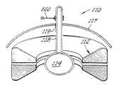
図面において、同様な符号は同様な部品を示す。図1乃至4に、ランプ−光ガイド間結合装置を100で総称して示す。結合装置100は、励起コイル112を有する形式の無電極高輝度放電(HID)ランプ110を含む。
励起コイル112は、2ターンが示されており、好ましくは、等脚台形を台形と同じ平面内に位置するが、台形と交差しないコイル中心線のまわりに回転することにより形成される容積を持つ図示の形状を有する。コイル形状の詳細や代替コイル形状が、たとえば米国特許第5,039,903号に記載されている。
【0009】
コイル112は発光管(アーク管)114を包囲し、発光管の上半部は、内部に向けられた可視光反射被膜116(斜線で示す)で被覆されている。(「上」、「下」などの相対的な方向を示す用語は、便宜的に使用しているだけで、限定の意味はない。)発光管114の下半部には、図示の実施例では被膜116は施されない。しかし、可視光反射被膜116が発光管114を覆う面積はもっと多くても少なくてもよい。正確な被覆面積は、HIDランプ110の動作を妨害することなく、発光管114から最大の光を抽出する光学的考察により決まり、当業者にとって周知の事項である。
【0010】
前述したように形成された被膜116は、耐火性で、したがってHIDランプ110の点灯中に遭遇する高温に耐える。反対に、金属被膜(たとえば、アルミニウムまたは銀)はこのような点灯温度で破損する。前述したように形成された被膜116は誘電性でもあり、したがって発光管中の電離可能な封入物を励起してアーク放電を生成する前述した電磁プロセスの間に短絡したり、電磁プロセスを妨害したりすることがない。
【0011】
被膜116は、光干渉フィルタから構成する場合、異なる周波数範囲の光を選択的に透過または反射するように設計することができる。したがって、光干渉フィルタから形成する場合、被膜116は、たとえば、可視光の望ましくない色または赤外光を透過するように設計することができる。所定の1組の高屈折率材料および低屈折率材料について層厚と層数を選択することにより、このような設計を実現する。これも当業界で通常の事項である。
【0012】
別の例では、可視光反射被膜116を、たとえば、アルミナ、マグネシアまたはチタニアのいずれかから形成した拡散反射被膜とすることができる。
発光管114は、電離(イオン化)可能な封入物(図示せず)を密封された空間内に収容している。無線周波(RF)電流をコイル112に流して電離可能な封入物を電磁的に励起して、発光管内にアーク放電(図示せず)を生成する。電離可能な封入物は、たとえば、ハロゲン化ナトリウム、ハロゲン化セリウムおよびキセノンを適当な重量割合で組み合わせて構成するのがよく、これにより可視放射光を発生し、白色の色温度で高い効率と良好な演色性を得る。また、ハロゲン化ランタン、ハロゲン化ナトリウム、ハロゲン化セリウムおよびバッファガスとしてキセノンまたはクリプトンの組み合わせからなる封入物も適当である。適当な封入物についての詳細は、米国特許第4,972,120号に記載されている。
【0013】
図示の実施例において、コイル112は、本質的に変圧器の一次巻線として作用し、一方発光管114内のアーク放電がこのような変圧器の1ターン(単巻)の二次巻線となる。コイル112に流れるRF電流は時間変動磁界を生成し、一方この磁界は電離可能な封入物に電界を生成し、その電界は完全に自身で閉じてソレノイド状電界を形成する。このようなソレノイド状電界の結果として流れる電流が、発光管にトロイダル、すなわちリング形状のアーク放電を誘起する。
【0014】
発光管114内にアーク放電を誘起するのに励起コイル112を使用する代わりに、たとえば容量性結合やマイクロ波放射を使用することができる。
図示の実施例において、HIDランプ110は、たとえばガスプローブよりなる始動補助器118を含む。ガスプローブ118は、クリプトンなどの電離可能な封入物を密封空間に収容した構成である。ガスプローブ118は、たとえば容量性結合スリーブ120を介して電気エネルギを受け取って、発光管114内での主アーク放電の始動を助ける。ガスプローブ始動補助器についての詳細は、米国特許第5,140,227号に記載されている。
【0015】
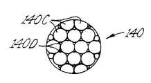
結合装置100は、HIDランプ110を光ガイド140に光学的に結合する中空な結合デバイス130を含む。可視光反射被膜116が、ランプ110から結合デバイス130への光の抽出を最大にするのに役立つ。光ガイド140は、図示のように、光ガイド部材(140A、140Bなど)の束からなり、各光ガイド部材は、たとえば既知のプラスチックまたはガラス光ガイドからなる。個別の光ガイド部材(140A、140Bなど)は、結合デバイス130の下側に示す中空端部内に収容するのが好ましい。光ガイド部材(140A、140Bなど)は、図1乃至4に示すように種々の寸法とするのが好ましく、また図2に示すようにわずかに圧縮するのが好ましい。寸法の異なる光ガイド部材を使用し、その終端部140Cを圧縮することにより、図2に140Dで示すような隣接する光ガイド部材間の隙間を最小にする。このような隙間(たとえば140D)はHIDランプ110から受け取った光を無駄にする。光ガイド部材(140A、140Bなど)はそれぞれランプから受け取った光を1つ以上の遠い位置に通常の態様で配給する。
【0016】
中空な結合デバイス130は、溶融石英などの中空な誘電部材から構成するのが好ましく、代表的には壁厚を1.5mmとする。結合デバイス130の入口端130Aは発光管114から光を受け取る。入口端130Aは、代表的には最大直径31mmであり、発光管114から約1mmのクリアランス132だけ離れている。このような寸法は、例示の値に過ぎず、この発明の範囲を限定するものではない。結合デバイス130はHIDランプ110から光を、第1の立体角で入口端130Aの第1の面積にわたって受け取り、その光を第1の立体角より小さい第2の立体角で、第1の面積より広い第2の面積にわたって出口端130Bに伝送する。この作用は角度−面積変換と称される。結合デバイス130は、この角度−面積変換を行うための、いわゆる複合放物面集光器(CPC=compound parabolic concentrator )を画定する形状とするのが好ましい。CPCは、たとえばW.T. Welford 及び R. Winston著の「HighCollection Nonimaging Optics」(New York,Academic Press,Inc.(1989))の第4章(pp.53−76)に詳しく説明されている。当業者には明らかなように、円錐形など他の形状の結合デバイスを用いてこのような角度−面積変換を行うこともできる。
【0017】
光をランプから光ガイドに移送するのに結合デバイス130を援助するために、結合デバイス130の内面(または外面)を可視光反射被膜150で被覆する。反射被膜150は光を結合デバイス130の内方に反射する作用をなす。反射被膜150は、前述した好適な可視光反射被膜116と同様に形成したフィルタから構成するのが好ましい。そうすれば、被膜150は、被膜116について上述した耐火性および誘電性を備える。
【0018】
中空な結合デバイス130は、たとえば20cmを越える長さを持つ様に形成して、発光管114から光ガイド140への熱伝達を最小にすることができる。この値は例示に過ぎず、他の値を用いてもよい。空間的な分離は発光管の寸法およびその内部で生成する放電にしたがって決定し、結合デバイス130の長さを発光管114の直径の4倍程度以上とする必要があることだけを理解しておけばよい。このような熱的分離により、特に光ガイド140をプラスチック材料から形成する場合に、光ガイド140の終端140Cを熱的ダメージから保護する。このような熱的分離によりさらに、光ガイド140がランプ110から有意な量の熱を抽出するのを防止する。このような熱の抽出があると、発光管114の熱分布が著しく非対称になり、ランプ性能がひどく劣化するおそれがある。結合デバイス130上の光反射被膜150は、光干渉フィルタから構成する場合、赤外光のスペクトルの大部分に対して透過性であり、熱が結合デバイス130の壁を通して逃げるのを許すので有利である。これにより結合デバイス130の長さを最小にすることができる。
【0019】
図3に示すHIDランプ110では、図1の発光管114上の光反射被膜116の代わりにだいたい球面状のミラー117を使用する。ミラー117は発光管114から光を受け取り、その光を下向きに結合デバイス130(図1)に向かって反射する。図示のように、ガスプローブ118をミラー117の孔119に貫通させるのがよい。所望に応じて、ミラー117をガスプローブ118に装着することができる。後述するこの発明の他の実施例でも、ミラー117を、発光管上の光反射被膜の代替品として使用することができる。
【0020】
図4に線図的に示すように、ランプ−光ガイド間結合装置100およびその関連回路(図示せず)を導電性エンクロージャ160に収容するのが有利である。このような導電性エンクロージャ160は、ランプ−光ガイド間結合装置100およびその関連回路が発生する、電磁干渉(EMI)の原因となるRF放射を、エンクロージャ内に実質的に閉じ込める。エンクロージャ160には孔162があり、そこを光ガイド140が通過し、光の分配が可能になる。孔162の寸法は、孔162から逃げ出すEMIを無視できる程度に抑えるのに十分な小さな寸法とするのが好ましい。このような孔の寸法を、励起手段(たとえばコイル112)の電磁エネルギの波長の約1/10以下とするのが好ましい。
【0021】
図5は、別のランプ−光ガイド間結合装置200を示す。結合装置200と図1の結合装置100との同様の部材は、最初の数字以外は同じ数の参照番号で示す。図5のHIDランプ210は、図1のHIDランプ110の上述した説明の通りである。
図5の結合装置200は、赤外線および紫外線の片方または両方を除去するかHIDランプ210の方へ反射して戻すフィルタ手段270を設けた点で、図1の結合装置100とは異なる。フィルタ手段270は、発光管214を光ガイド240から熱的に分離するのを助け、これがなければUVまたはIR放射線への露出からもたらされるであろう光ガイドの端部へのダメージを防止する。
【0022】
フィルタ手段270は、たとえば、光学的干渉被膜で被覆された平坦な石英ディスクからなる。干渉被膜をディスクの両面に設けてもよく、好ましくは前述した光反射被膜116とほぼ同じ方法で形成する。図6から明らかなように、フィルタ手段270は、結合デバイスの上側部分231と結合デバイスの下側部分231Bの棚部271との間に配置するのがよい。同じく図6に示すように、結合デバイスの上側部分231Aが結合デバイスの下側部分231B内に収容されており、これはこれら両部分を連結する好都合な方法の一つである。
【0023】
図7は、発光管314の底部315がほぼ平坦である別のランプ−光ガイド間結合装置300を示す。平坦な底部により、発光管314からの光分配が改良される。
図8は、平坦な底部415を有する発光管414を用いた他の実施例のランプ−光ガイド間結合装置400を示す。結合装置400はさらに、たとえば溶融石英から形成した耐火性の中間ロッドまたは柱状体480を含む。耐火性の中間ロッド480の下端は結合デバイスの入口端430Aに収容されている。耐火性の中間ロッドの上端は平坦な窓すなわち底部415に近接して配置されており、好ましくは底部415から熱的分離ギャップ490だけ離されている。
【0024】
中間ロッド480は、HIDランプ410を光ガイド(図8には図示せず)から熱的にさらに分離する役目を果たす。これにより、「下流側」の光分配要素、たとえば結合デバイス430の熱的設計条件が緩和される。
上述したところから明らかなように、この発明は、ランプの光の大部分を光ガイドに光学的に効率のよい態様で伝送する無電極HIDランプ用ランプ−光ガイド間結合装置を提供する。結合装置には誘電材料を用いるのが好ましく、これにより、結合装置を破壊したり、ランプ動作を妨害したりするおそれのある短絡電流が防止される。ランプからの熱エネルギのもれを最小限に抑えて、ランプから光が抽出され、このためランプの熱分布が著しく非対称になる(ランプ動作を損なう恐れがある)のが防止される。光ガイドの加熱が、種々の方法で最小にされる。たとえば、中空な結合デバイスを用いることにより、またこのような結合デバイスの長さを調節することにより、あるいは希望に応じて、結合デバイス上に赤外線に対して透明な可視光反射被膜を設けることにより、光ガイドの加熱が最小にされる。
【0025】
以上、この発明を例示のために特定の実施例に関して説明したが、当業者には種々の変形や変更が明らかである。したがって、特許請求の範囲は、このような変更例や変形例のすべてがこの発明の範囲に包含されると解すべきである。
たとえば、反射被膜116を発光管114から取り除き、130と同様な第2の光カップラ(結合デバイス)を発光管114の反対側に配置することが可能である。この第2の結合デバイスを設ける場合、始動用プローブ118を該結合デバイスの中心に貫通させるか、または該結合デバイスの軸線からはずれるが、コイル112を邪魔しない傾斜した位置に移動することができる。このような例では、始動用プローブが結合デバイスの側面に形成した開口を貫通する様にすることができる。
【図面の簡単な説明】
【図1】この発明の第1実施例によるHIDランプ用のランプ−光ガイド間結合装置を一部破断して示す斜視図である。
【図2】図1のHIDランプから光を受け取る光ガイド部材の束からなる光ガイドの端部を縮小して示す断面図である。
【図3】図1のランプ−光ガイド間結合装置に用いることができる、ランプの発光管から上向きに出てくる光を下向きに向けなおす球面状ミラーを用いるHIDランプの別例を一部破断して示す斜視図である。
【図4】無電極HIDランプ用のランプ−光ガイド間結合装置を収容する導電性エンクロージャの線図的斜視図である。
【図5】赤外線や紫外線などの非可視光を反射してHIDランプの方へ戻す手段を含むランプ−光ガイド間結合装置を一部破断して示す斜視図である。
【図6】図5の非可視光反射手段を結合デバイスの上側部分と下側部分との間に配置する仕方を示す、結合装置の一部の断面図である。
【図7】HIDランプに光抽出用の平坦な表面を有する発光管を用いたランプ−光ガイド間結合装置の実施例を一部破断して示す斜視図である。
【図8】図7と同様な、光抽出用に平坦な窓を有する発光管を用い、このような平坦な窓から結合装置の中空な結合デバイスへ光を伝送するのに耐火性の中間ロッドを用いたランプ−光ガイド間結合装置の実施例を示す斜視図である。
【符号の説明】
100 ランプ−光ガイド間結合装置
110 HIDランプ
112 コイル
114 発光管
116 可視光反射被膜
117 ミラー
118 ガスプローブ
130 結合デバイス
140 光ガイド
150 可視光反射被膜
160 導電性エンクロージャ
270 フィルタ手段[0001]
[Industrial application fields]
The present invention relates to a coupling device that receives light from a lamp and delivers the light to a light guide for delivering light to one or more remote locations. In particular, the present invention relates to a lamp-light guide coupling device suitable for use with an electrodeless high intensity discharge lamp.
[0002]
[Prior art]
Coupling devices that receive light from various types of lamps and send the light to a light guide are well known. An example of such a coupling device is described in US Pat. No. 5,199,091. Another example can be found in US patent application Ser. No. 07 / 859,180 (Japanese Patent Application No. 5-064907). However, when the lamp-light guide coupling device is used together with an electrodeless high intensity discharge (HID) lamp, a special problem arises due to the nature of such a lamp.
[0003]
The electrodeless HID lamp is configured to contain an ionizable (ionized) inclusion in an arc chamber. The ionizable enclosure is electrically excited from outside the arc chamber to induce arc discharge in the enclosure. This can be achieved, for example, with an excitation coil that surrounds the arc tube (arc tube), which generates a radio frequency (RF) magnetic field, thereby creating a solenoidal electric field within the ionizable enclosure. Induce. The current flowing through the enclosure as a result of such a solenoidal electric field induces an arc discharge in the enclosure. See US Pat. No. 4,810,938 for a more detailed description of such lamps. In order to prevent high frequency magnetic fields from generating short circuit currents in the lamp-light guide coupling device, it is preferred to use a dielectric material in such a device. Such short circuit currents can destroy the coupling device and can interfere with the process of exciting the ionizable enclosure in the arc tube and creating an arc discharge there.
[0004]
Further, the arc tube of the electrodeless HID lamp typically becomes high temperature, for example, 900 ° C. during operation. A suitable coupling device extracts light from the arc tube of such a lamp, minimizing the leakage of thermal energy from the lamp. This prevents the heat distribution of the lamp from becoming a highly asymmetric heat distribution that can severely degrade the operation of the lamp.
[0005]
OBJECT OF THE INVENTION
Accordingly, it is an object of the present invention to provide a lamp-light guide coupling device for an electrodeless HID lamp, preferably using a dielectric material.
Another object of the present invention is to provide a lamp-light guide coupling device for an electrodeless HID lamp, in which the light is extracted from the lamp and the leakage of heat energy from the lamp is minimized. It is intended to minimize the heating that leads to the destruction of the light guide by avoiding a significantly asymmetric heat distribution that can severely degrade the operation of the light guide, and avoiding significant heat energy outflow.
[0006]
SUMMARY OF THE INVENTION
In one embodiment of the present invention, a lamp-light guide coupling device is provided. The coupling device of the present invention includes an electrodeless high intensity discharge lamp. The discharge lamp includes an arc tube containing an ionizable enclosure, and excitation means for electrically exciting the ionizable enclosure and inducing a luminescent arc discharge therein. The coupling device further includes a coupling device comprised of a generally tubular hollow body having an inlet end for receiving light from the arc discharge and a larger outlet end. The coupling device further comprises inwardly reflecting means for reflecting visible light on the surface of the hollow body. The coupling device is configured to receive light over an area at the entrance end at a solid angle and transmit light over an area at the exit end that is smaller than the solid angle and wider than the area. The coupling device is preferably formed from a dielectric material, thus avoiding the occurrence of short circuit currents. Such devices extract only a minimal amount of heat from the lamp when extracting the lamp light.
[0007]
The lamp-light guide coupling device for an electrodeless HID lamp described above transmits most of the light from the lamp to the light guide in an optically efficient manner.
In order to further clarify the above and other objects and effects of the present invention, a preferred embodiment shown in the drawings will be described below.
[0008]
DESCRIPTION OF PREFERRED EMBODIMENTS
In the drawings, like numerals indicate like parts. 1 to 4, a lamp-light guide coupling device is generally indicated by 100. The
[0009]
The
[0010]
The
[0011]
When the
[0012]
In another example, the visible light
The
[0013]
In the illustrated embodiment, the
[0014]
Instead of using the
In the illustrated embodiment, the
[0015]
The
[0016]
The hollow coupling device 130 is preferably composed of a hollow dielectric member such as fused quartz, and typically has a wall thickness of 1.5 mm. The
[0017]
To assist the coupling device 130 in transferring light from the lamp to the light guide, the inner surface (or outer surface) of the coupling device 130 is coated with a visible light
[0018]
The hollow coupling device 130 can be formed to have a length of, for example, greater than 20 cm to minimize heat transfer from the
[0019]
In the
[0020]
As shown diagrammatically in FIG. 4, the lamp-to-light
[0021]
FIG. 5 shows another lamp-light
The
[0022]
Filter means 270 consists of, for example, a flat quartz disk coated with an optical interference coating. An interference coating may be provided on both sides of the disk, and is preferably formed by substantially the same method as the light reflection coating 116 described above. As is apparent from FIG. 6, the filter means 270 may be disposed between the upper part 231 of the coupling device and the
[0023]
FIG. 7 shows another lamp-light
FIG. 8 shows another embodiment of a lamp-light
[0024]
As is apparent from the above, the present invention provides a lamp-light guide coupling device for an electrodeless HID lamp that transmits most of the light of the lamp to the light guide in an optically efficient manner. A dielectric material is preferably used for the coupling device, which prevents short circuit currents that could destroy the coupling device or interfere with lamp operation. Leakage of thermal energy from the lamp is minimized and light is extracted from the lamp, thus preventing the lamp heat distribution from becoming significantly asymmetric (which can impair lamp operation). The heating of the light guide is minimized in various ways. For example, by using a hollow coupling device, adjusting the length of such a coupling device, or, if desired, providing a visible light reflective coating that is transparent to infrared radiation on the coupling device. The heating of the light guide is minimized.
[0025]
Although the invention has been described with respect to particular embodiments for purposes of illustration, various modifications and changes will become apparent to those skilled in the art. Therefore, it is to be understood that the appended claims include all such modifications and variations as fall within the scope of the invention.
For example, the
[Brief description of the drawings]
FIG. 1 is a partially cutaway perspective view showing a lamp-light guide coupling device for an HID lamp according to a first embodiment of the present invention.
2 is a cross-sectional view showing a reduced end portion of a light guide formed of a bundle of light guide members that receive light from the HID lamp of FIG. 1;
FIG. 3 is a partially broken view of another example of an HID lamp using a spherical mirror that can be used in the lamp-light guide coupling device of FIG. 1 and redirects light emitted upward from the arc tube of the lamp. It is a perspective view shown.
FIG. 4 is a diagrammatic perspective view of a conductive enclosure containing a lamp-light guide coupling device for an electrodeless HID lamp.
FIG. 5 is a perspective view showing a partially broken lamp-light guide coupling device including means for reflecting non-visible light such as infrared rays and ultraviolet rays and returning them to the HID lamp.
6 is a cross-sectional view of a part of the coupling device showing how the non-visible light reflecting means of FIG. 5 is arranged between the upper part and the lower part of the coupling device.
FIG. 7 is a partially cutaway perspective view of an embodiment of a lamp-light guide coupling device using an arc tube having a flat surface for light extraction as an HID lamp.
8 uses a light emitting tube with a flat window for light extraction, similar to FIG. 7, and a refractory intermediate rod for transmitting light from such a flat window to the hollow coupling device of the coupling device; It is a perspective view which shows the Example of the coupling | bonding apparatus between the lamp | ramp and light guides using A.
[Explanation of symbols]
100 lamp-light
Claims (15)
Translated fromJapanese(a)前記無電極放電ランプとほぼ同じ断面積を有し、前記放電ランプに近接して配置され、前記アーク放電から光を受け取る入口端と該入口端より大きい出口端を有する略管状の中空の構成の結合デバイスと、
(b)前記中空の結合デバイスの表面の少なくとも一部に配置され、光を前記結合デバイスの内部に反射する反射手段と、
(c)前記中空の結合デバイスの出口端に連結された少なくとも1つの光ガイドとを含み、
(d)前記結合デバイスの形状は、前記入口端において第1の立体角で光を受け取り、光を前記第1の立体角より小さい第2の立体角で前記出口端に伝送するように成形された形状であり、
(e)前記放電ランプに近接して配置される前記結合デバイスは、前記放電ランプの熱的および電気的作動特性に実質的な影響を及ぼさず、
(f)前記ランプの発光管の光透過側が前記中空の結合デバイスの入口端内に収容されていることを特徴とする、光結合装置。In an optical coupling device for an electrodeless discharge lamp having an arc tube enclosing an ionizable enclosure that can be excited to generate a luminous arc discharge and having predetermined thermal and electrical operating characteristics,
(A) a substantially tubular hollow having substantially the same cross-sectional area as the electrodeless discharge lamp, disposed close to the discharge lamp, and having an inlet end for receiving light from the arc discharge and an outlet end larger than the inlet end A coupling device of the configuration of
(B) reflecting means disposed on at least a part of the surface of the hollow coupling device and reflecting light into the coupling device;
(C) at least one light guide coupled to the outlet end of the hollow coupling device;
(D) The shape of the coupling device is shaped to receive light at a first solid angle at the inlet end and transmit light to the outlet end at a second solid angle that is smaller than the first solid angle. Shape
(E) the coupling device disposed in proximity to the discharge lamp doesnot substantially affect the thermal and electrical operating characteristics of the discharge lamp;
(F) The light coupling device, wherein the light transmission side of the arc tube of the lamp is accommodated in the inlet end of the hollow coupling device.
(a)電離可能な封入物を入れた発光管を含む無電極高輝度放電ランプと、
(b)前記発光管を包囲し、前記電離可能な封入物を電磁的に励起して前記発光管内に発光性アーク放電を誘起する励起コイルと、
(c)(i)前記アーク放電から光を受け取る入口端、および入口端より大きい出口端を持つだいたい管状の本体を有し、(ii)非導電性かつ、全内部反射特性を有し、(iii)光を前記入口端において第1の立体角で受け取り、その光を前記第1の立体角より小さい第2の立体角で前記出口端に伝送する様に成形されている結合デバイスと、
(d)前記結合デバイスの出口端に連結された少なくとも1つの光ガイドとを含み、
(e)前記発光管の光透過側が前記結合デバイスの入口端内に収容されている光分配装置。In a light distribution device for transmitting light output from an electrodeless high intensity discharge lamp to at least one remote location,
(A) an electrodeless high-intensity discharge lamp including an arc tube containing an ionizable enclosure;
(B) an excitation coil that surrounds the arc tube and electromagnetically excites the ionizable enclosure to induce a luminescent arc discharge in the arc tube;
(C) (i) having a generally tubular body having an inlet end for receiving light from the arc discharge and an outlet end larger than the inlet end; (ii) non-conductive and having total internal reflection properties; iii) a coupling device that is shaped to receive light at the first solid angle at the inlet end and transmit the light to the outlet end at a second solid angle that is smaller than the first solid angle;
(D) at least one light guide coupled to the outlet end of the coupling device;
(E) A light distribution devicein which a light transmission side of the arc tube is accommodated in an inlet end of the coupling device .
Applications Claiming Priority (2)
| Application Number | Priority Date | Filing Date | Title |
|---|---|---|---|
| US16576093A | 1993-12-10 | 1993-12-10 | |
| US165760 | 1993-12-10 |
Publications (2)
| Publication Number | Publication Date |
|---|---|
| JPH07270625A JPH07270625A (en) | 1995-10-20 |
| JP3663223B2true JP3663223B2 (en) | 2005-06-22 |
Family
ID=22600347
Family Applications (1)
| Application Number | Title | Priority Date | Filing Date |
|---|---|---|---|
| JP30254594AExpired - Fee RelatedJP3663223B2 (en) | 1993-12-10 | 1994-12-07 | Optical coupling device and light distribution device for electrodeless discharge lamp |
Country Status (2)
| Country | Link |
|---|---|
| US (1) | US5675677A (en) |
| JP (1) | JP3663223B2 (en) |
Families Citing this family (26)
| Publication number | Priority date | Publication date | Assignee | Title |
|---|---|---|---|---|
| AT405212B (en)* | 1997-01-15 | 1999-06-25 | Photonic Optische Geraete Gmbh | OPTICAL ELEMENT |
| US5812714A (en)* | 1997-01-30 | 1998-09-22 | Cooper Industries, Inc. | Optical waveguide elements for a distributed lighting system |
| US6027237A (en)* | 1997-03-17 | 2000-02-22 | Remote Source Lighting International, Inc. | Air router for cooling light guide bundle |
| JPH10322519A (en)* | 1997-05-16 | 1998-12-04 | Nikon Corp | Illumination device and image reading device |
| US6238074B1 (en) | 1997-12-09 | 2001-05-29 | Cooper Automotive Products, Inc. | Optical waveguide structures |
| US6168302B1 (en) | 1997-12-09 | 2001-01-02 | Cooper Automotive Products, Inc. | Hybrid distributed lighting system for a vehicle |
| US6193399B1 (en) | 1997-12-09 | 2001-02-27 | Cooper Automotive Products, Inc. | Optical waveguide structures for vehicle lighting |
| US6220713B1 (en) | 1998-10-23 | 2001-04-24 | Compaq Computer Corporation | Projection lens and system |
| US7385357B2 (en) | 1999-06-21 | 2008-06-10 | Access Business Group International Llc | Inductively coupled ballast circuit |
| US7126450B2 (en) | 1999-06-21 | 2006-10-24 | Access Business Group International Llc | Inductively powered apparatus |
| US7612528B2 (en) | 1999-06-21 | 2009-11-03 | Access Business Group International Llc | Vehicle interface |
| US6825620B2 (en) | 1999-06-21 | 2004-11-30 | Access Business Group International Llc | Inductively coupled ballast circuit |
| US6731071B2 (en) | 1999-06-21 | 2004-05-04 | Access Business Group International Llc | Inductively powered lamp assembly |
| US6546752B2 (en)* | 1999-12-02 | 2003-04-15 | Fiberstars Incorporated | Method of making optical coupling device |
| US6304693B1 (en) | 1999-12-02 | 2001-10-16 | Fiberstars Incorporated | Efficient arrangement for coupling light between light source and light guide |
| US6302571B1 (en) | 2000-03-30 | 2001-10-16 | Fiberstars Incorporated | Waterproof system for delivering light to a light guide |
| DE10211015A1 (en)* | 2002-03-13 | 2003-09-25 | Philips Intellectual Property | reflector lamp |
| US7220035B2 (en)* | 2003-03-07 | 2007-05-22 | Fiberstars, Inc. | Compact, high-efficiency illumination system for video-imaging devices |
| US6942373B2 (en)* | 2003-03-14 | 2005-09-13 | Fiberstars Incorporated | Fiberoptic lighting system with shaped collector for efficiency |
| US7252406B2 (en)* | 2003-04-04 | 2007-08-07 | Purespectrum Llc | Fluorescent lamp system using reflectors |
| US7462951B1 (en) | 2004-08-11 | 2008-12-09 | Access Business Group International Llc | Portable inductive power station |
| US7408324B2 (en) | 2004-10-27 | 2008-08-05 | Access Business Group International Llc | Implement rack and system for energizing implements |
| US20070200505A1 (en)* | 2005-12-27 | 2007-08-30 | Ju Gao | Projection light source and methods of manufacture |
| US7854614B2 (en)* | 2007-12-14 | 2010-12-21 | Robb John R | Multi-contact universally jointed power and/or signal connector devices |
| US8382323B2 (en) | 2007-12-14 | 2013-02-26 | John R. Robb | Individually controllable multi-color illumination units |
| DE102009048830B4 (en)* | 2009-10-09 | 2012-01-12 | Osram Gesellschaft mit beschränkter Haftung | Lichtleitstruktur |
Family Cites Families (11)
| Publication number | Priority date | Publication date | Assignee | Title |
|---|---|---|---|---|
| US4002499A (en)* | 1974-07-26 | 1977-01-11 | The United States Of America As Represented By The United States Energy Research And Development Administration | Radiant energy collector |
| US4810938A (en)* | 1987-10-01 | 1989-03-07 | General Electric Company | High efficacy electrodeless high intensity discharge lamp |
| US4890042A (en)* | 1988-06-03 | 1989-12-26 | General Electric Company | High efficacy electrodeless high intensity discharge lamp exhibiting easy starting |
| US4972120A (en)* | 1989-05-08 | 1990-11-20 | General Electric Company | High efficacy electrodeless high intensity discharge lamp |
| US5039903A (en)* | 1990-03-14 | 1991-08-13 | General Electric Company | Excitation coil for an electrodeless high intensity discharge lamp |
| EP0450131B1 (en)* | 1990-04-06 | 1995-08-02 | New Japan Radio Co., Ltd. | Electrodeless microwave-generated radiation apparatus |
| US5113121A (en)* | 1990-05-15 | 1992-05-12 | Gte Laboratories Incorporated | Electrodeless HID lamp with lamp capsule |
| US5140227A (en)* | 1990-12-04 | 1992-08-18 | General Electric Company | Starting aid for an electrodeless high intensity discharge lamp |
| US5117312A (en)* | 1991-01-04 | 1992-05-26 | Fusion Systems Corporation | Apparatus including concave reflectors and a line of optical fibers |
| US5199091A (en)* | 1991-12-13 | 1993-03-30 | General Electric Company | Arrangement and a method for coupling a light source to a light guide using a solid optical coupler |
| US5271077A (en)* | 1992-09-09 | 1993-12-14 | Gte Products Corporation | Nonimaging reflector for coupling light into a light pipe |
- 1994
- 1994-12-07JPJP30254594Apatent/JP3663223B2/ennot_activeExpired - Fee Related
- 1995
- 1995-05-26USUS08/451,625patent/US5675677A/ennot_activeExpired - Fee Related
Also Published As
| Publication number | Publication date |
|---|---|
| JPH07270625A (en) | 1995-10-20 |
| US5675677A (en) | 1997-10-07 |
Similar Documents
| Publication | Publication Date | Title |
|---|---|---|
| JP3663223B2 (en) | Optical coupling device and light distribution device for electrodeless discharge lamp | |
| RU2190283C2 (en) | Light emission method and device | |
| US7940007B2 (en) | Plasma lamp with dielectric waveguide integrated with transparent bulb | |
| US7429818B2 (en) | Plasma lamp with bulb and lamp chamber | |
| US5519285A (en) | Electrodeless discharge lamp | |
| EP0447852B1 (en) | Luminaire for an electrodeless high intensity discharge lamp with electromagnetic interference shielding | |
| KR20020006538A (en) | High brightness microwave lamp | |
| EP0990248B1 (en) | Unit comprising a short-arc discharge lamp with a starting antenna | |
| CN102224564B (en) | Microwave light source with solid dielectric waveguide | |
| US8629616B2 (en) | Arc tube device and stem structure for electrodeless plasma lamp | |
| EP0541344B1 (en) | Luminaire including an electrodeless discharge lamp as a light source | |
| EP0404593B1 (en) | Luminaire for an electrodeless high intensity discharge lamp | |
| JP4120585B2 (en) | Electrodeless low-pressure lamp with many ferrite cores and induction coils | |
| GB1583283A (en) | Electrodeless fluorescent lamps | |
| GB2221568A (en) | Capacitive starting electrodes for electrodeless lamps | |
| NL7901897A (en) | ELECTRESSLESS GAS DISCHARGE LAMP. | |
| JP2001266803A (en) | Electrodeless discharge lamp | |
| JPH07192703A (en) | Radio maximum high brightness discharge lamp | |
| JPH11317205A (en) | Electrodeless lamp assembly, coaxial applicator for high intensity discharge lamp and electrodeless power source | |
| US20050094940A1 (en) | Integrated light source and optical waveguide and method | |
| EP0458544A2 (en) | A starting aid for an electrodeless high intensity discharge lamp | |
| JPH10321194A (en) | Electrodeless discharge lamp | |
| JP2002164188A (en) | Microwave electrodeless discharge lamp device | |
| EP0550985A1 (en) | High intensity discharge lamp and excitation coil configuration | |
| JP3849613B2 (en) | Electrodeless discharge lamp, electrodeless discharge lamp lighting device and lighting device |
Legal Events
| Date | Code | Title | Description |
|---|---|---|---|
| A601 | Written request for extension of time | Free format text:JAPANESE INTERMEDIATE CODE: A601 Effective date:20040205 | |
| A602 | Written permission of extension of time | Free format text:JAPANESE INTERMEDIATE CODE: A602 Effective date:20040217 | |
| A521 | Written amendment | Free format text:JAPANESE INTERMEDIATE CODE: A523 Effective date:20040506 | |
| A02 | Decision of refusal | Free format text:JAPANESE INTERMEDIATE CODE: A02 Effective date:20041012 | |
| A521 | Written amendment | Free format text:JAPANESE INTERMEDIATE CODE: A523 Effective date:20050107 | |
| A911 | Transfer to examiner for re-examination before appeal (zenchi) | Free format text:JAPANESE INTERMEDIATE CODE: A911 Effective date:20050209 | |
| TRDD | Decision of grant or rejection written | ||
| A01 | Written decision to grant a patent or to grant a registration (utility model) | Free format text:JAPANESE INTERMEDIATE CODE: A01 Effective date:20050301 | |
| A61 | First payment of annual fees (during grant procedure) | Free format text:JAPANESE INTERMEDIATE CODE: A61 Effective date:20050328 | |
| R150 | Certificate of patent or registration of utility model | Free format text:JAPANESE INTERMEDIATE CODE: R150 | |
| LAPS | Cancellation because of no payment of annual fees |