JP3661669B2 - Active matrix substrate, electro-optical device, electronic equipment - Google Patents
Active matrix substrate, electro-optical device, electronic equipmentDownload PDFInfo
- Publication number
- JP3661669B2 JP3661669B2JP2002212762AJP2002212762AJP3661669B2JP 3661669 B2JP3661669 B2JP 3661669B2JP 2002212762 AJP2002212762 AJP 2002212762AJP 2002212762 AJP2002212762 AJP 2002212762AJP 3661669 B2JP3661669 B2JP 3661669B2
- Authority
- JP
- Japan
- Prior art keywords
- active matrix
- matrix substrate
- data line
- line
- scanning line
- Prior art date
- Legal status (The legal status is an assumption and is not a legal conclusion. Google has not performed a legal analysis and makes no representation as to the accuracy of the status listed.)
- Expired - Fee Related
Links
- 239000000758substrateSubstances0.000titleclaimsdescription128
- 239000011159matrix materialSubstances0.000titleclaimsdescription48
- 239000010408filmSubstances0.000claimsdescription110
- 239000010410layerSubstances0.000claimsdescription110
- 239000004065semiconductorSubstances0.000claimsdescription36
- 239000003990capacitorSubstances0.000claimsdescription32
- 239000011229interlayerSubstances0.000claimsdescription31
- 238000003860storageMethods0.000claimsdescription28
- 229910052751metalInorganic materials0.000claimsdescription22
- 239000002184metalSubstances0.000claimsdescription22
- 239000000463materialSubstances0.000claimsdescription21
- 239000010409thin filmSubstances0.000claimsdescription16
- 230000015572biosynthetic processEffects0.000claimsdescription7
- 229910021420polycrystalline siliconInorganic materials0.000claimsdescription6
- 230000000149penetrating effectEffects0.000claimsdescription3
- 239000004973liquid crystal related substanceSubstances0.000description63
- 238000000034methodMethods0.000description11
- 230000000694effectsEffects0.000description8
- 230000005684electric fieldEffects0.000description8
- 239000003086colorantSubstances0.000description7
- 230000008878couplingEffects0.000description6
- 238000010168coupling processMethods0.000description6
- 238000005859coupling reactionMethods0.000description6
- 239000003566sealing materialSubstances0.000description6
- 230000008569processEffects0.000description5
- 229910052782aluminiumInorganic materials0.000description4
- XAGFODPZIPBFFR-UHFFFAOYSA-NaluminiumChemical compound[Al]XAGFODPZIPBFFR-UHFFFAOYSA-N0.000description4
- 239000000470constituentSubstances0.000description4
- 230000002093peripheral effectEffects0.000description4
- NRTOMJZYCJJWKI-UHFFFAOYSA-NTitanium nitrideChemical compound[Ti]#NNRTOMJZYCJJWKI-UHFFFAOYSA-N0.000description3
- PMHQVHHXPFUNSP-UHFFFAOYSA-Mcopper(1+);methylsulfanylmethane;bromideChemical compoundBr[Cu].CSCPMHQVHHXPFUNSP-UHFFFAOYSA-M0.000description3
- 230000006866deteriorationEffects0.000description3
- 238000010586diagramMethods0.000description3
- 239000011521glassSubstances0.000description3
- 239000010936titaniumSubstances0.000description3
- 230000005540biological transmissionEffects0.000description2
- 230000000903blocking effectEffects0.000description2
- 230000015556catabolic processEffects0.000description2
- 210000002858crystal cellAnatomy0.000description2
- 230000007547defectEffects0.000description2
- 238000006731degradation reactionMethods0.000description2
- 238000005401electroluminescenceMethods0.000description2
- 238000005530etchingMethods0.000description2
- 239000012535impuritySubstances0.000description2
- 238000004519manufacturing processMethods0.000description2
- 238000005498polishingMethods0.000description2
- 229920001721polyimidePolymers0.000description2
- 239000010453quartzSubstances0.000description2
- 230000009467reductionEffects0.000description2
- 239000011347resinSubstances0.000description2
- 229920005989resinPolymers0.000description2
- 230000000630rising effectEffects0.000description2
- 238000005070samplingMethods0.000description2
- VYPSYNLAJGMNEJ-UHFFFAOYSA-Nsilicon dioxideInorganic materialsO=[Si]=OVYPSYNLAJGMNEJ-UHFFFAOYSA-N0.000description2
- WQJQOUPTWCFRMM-UHFFFAOYSA-Ntungsten disilicideChemical compound[Si]#[W]#[Si]WQJQOUPTWCFRMM-UHFFFAOYSA-N0.000description2
- 229910021342tungsten silicideInorganic materials0.000description2
- 239000004988Nematic liquid crystalSubstances0.000description1
- XUIMIQQOPSSXEZ-UHFFFAOYSA-NSiliconChemical compound[Si]XUIMIQQOPSSXEZ-UHFFFAOYSA-N0.000description1
- RTAQQCXQSZGOHL-UHFFFAOYSA-NTitaniumChemical compound[Ti]RTAQQCXQSZGOHL-UHFFFAOYSA-N0.000description1
- 239000000853adhesiveSubstances0.000description1
- 230000001070adhesive effectEffects0.000description1
- 230000002411adverseEffects0.000description1
- 229910021417amorphous siliconInorganic materials0.000description1
- 239000011324beadSubstances0.000description1
- 210000004027cellAnatomy0.000description1
- 230000008859changeEffects0.000description1
- 238000004140cleaningMethods0.000description1
- 239000004020conductorSubstances0.000description1
- 238000011109contaminationMethods0.000description1
- 230000007797corrosionEffects0.000description1
- 238000005260corrosionMethods0.000description1
- 238000000151depositionMethods0.000description1
- 230000009977dual effectEffects0.000description1
- 239000003365glass fiberSubstances0.000description1
- 229910052736halogenInorganic materials0.000description1
- 150000002367halogensChemical class0.000description1
- 238000010438heat treatmentMethods0.000description1
- 239000007943implantSubstances0.000description1
- AMGQUBHHOARCQH-UHFFFAOYSA-Nindium;oxotinChemical compound[In].[Sn]=OAMGQUBHHOARCQH-UHFFFAOYSA-N0.000description1
- 238000007689inspectionMethods0.000description1
- 230000014759maintenance of locationEffects0.000description1
- 230000007257malfunctionEffects0.000description1
- 150000002739metalsChemical class0.000description1
- 230000004048modificationEffects0.000description1
- 238000012986modificationMethods0.000description1
- 229910021421monocrystalline siliconInorganic materials0.000description1
- 230000003287optical effectEffects0.000description1
- 238000000016photochemical curingMethods0.000description1
- 230000001681protective effectEffects0.000description1
- 229910052710siliconInorganic materials0.000description1
- 239000010703siliconSubstances0.000description1
- 239000000126substanceSubstances0.000description1
- 229920001187thermosetting polymerPolymers0.000description1
- 229910052719titaniumInorganic materials0.000description1
- MAKDTFFYCIMFQP-UHFFFAOYSA-Ntitanium tungstenChemical compound[Ti].[W]MAKDTFFYCIMFQP-UHFFFAOYSA-N0.000description1
Images


Classifications
- G—PHYSICS
- G02—OPTICS
- G02F—OPTICAL DEVICES OR ARRANGEMENTS FOR THE CONTROL OF LIGHT BY MODIFICATION OF THE OPTICAL PROPERTIES OF THE MEDIA OF THE ELEMENTS INVOLVED THEREIN; NON-LINEAR OPTICS; FREQUENCY-CHANGING OF LIGHT; OPTICAL LOGIC ELEMENTS; OPTICAL ANALOGUE/DIGITAL CONVERTERS
- G02F1/00—Devices or arrangements for the control of the intensity, colour, phase, polarisation or direction of light arriving from an independent light source, e.g. switching, gating or modulating; Non-linear optics
- G02F1/01—Devices or arrangements for the control of the intensity, colour, phase, polarisation or direction of light arriving from an independent light source, e.g. switching, gating or modulating; Non-linear optics for the control of the intensity, phase, polarisation or colour
- G02F1/13—Devices or arrangements for the control of the intensity, colour, phase, polarisation or direction of light arriving from an independent light source, e.g. switching, gating or modulating; Non-linear optics for the control of the intensity, phase, polarisation or colour based on liquid crystals, e.g. single liquid crystal display cells
- G02F1/133—Constructional arrangements; Operation of liquid crystal cells; Circuit arrangements
- G02F1/136—Liquid crystal cells structurally associated with a semi-conducting layer or substrate, e.g. cells forming part of an integrated circuit
- G02F1/1362—Active matrix addressed cells
- G02F1/136286—Wiring, e.g. gate line, drain line
- G—PHYSICS
- G02—OPTICS
- G02F—OPTICAL DEVICES OR ARRANGEMENTS FOR THE CONTROL OF LIGHT BY MODIFICATION OF THE OPTICAL PROPERTIES OF THE MEDIA OF THE ELEMENTS INVOLVED THEREIN; NON-LINEAR OPTICS; FREQUENCY-CHANGING OF LIGHT; OPTICAL LOGIC ELEMENTS; OPTICAL ANALOGUE/DIGITAL CONVERTERS
- G02F1/00—Devices or arrangements for the control of the intensity, colour, phase, polarisation or direction of light arriving from an independent light source, e.g. switching, gating or modulating; Non-linear optics
- G02F1/01—Devices or arrangements for the control of the intensity, colour, phase, polarisation or direction of light arriving from an independent light source, e.g. switching, gating or modulating; Non-linear optics for the control of the intensity, phase, polarisation or colour
- G02F1/13—Devices or arrangements for the control of the intensity, colour, phase, polarisation or direction of light arriving from an independent light source, e.g. switching, gating or modulating; Non-linear optics for the control of the intensity, phase, polarisation or colour based on liquid crystals, e.g. single liquid crystal display cells
- G02F1/133—Constructional arrangements; Operation of liquid crystal cells; Circuit arrangements
- G02F1/136—Liquid crystal cells structurally associated with a semi-conducting layer or substrate, e.g. cells forming part of an integrated circuit
- G02F1/1362—Active matrix addressed cells
- G02F1/136227—Through-hole connection of the pixel electrode to the active element through an insulation layer
- G—PHYSICS
- G02—OPTICS
- G02F—OPTICAL DEVICES OR ARRANGEMENTS FOR THE CONTROL OF LIGHT BY MODIFICATION OF THE OPTICAL PROPERTIES OF THE MEDIA OF THE ELEMENTS INVOLVED THEREIN; NON-LINEAR OPTICS; FREQUENCY-CHANGING OF LIGHT; OPTICAL LOGIC ELEMENTS; OPTICAL ANALOGUE/DIGITAL CONVERTERS
- G02F1/00—Devices or arrangements for the control of the intensity, colour, phase, polarisation or direction of light arriving from an independent light source, e.g. switching, gating or modulating; Non-linear optics
- G02F1/01—Devices or arrangements for the control of the intensity, colour, phase, polarisation or direction of light arriving from an independent light source, e.g. switching, gating or modulating; Non-linear optics for the control of the intensity, phase, polarisation or colour
- G02F1/13—Devices or arrangements for the control of the intensity, colour, phase, polarisation or direction of light arriving from an independent light source, e.g. switching, gating or modulating; Non-linear optics for the control of the intensity, phase, polarisation or colour based on liquid crystals, e.g. single liquid crystal display cells
- G02F1/133—Constructional arrangements; Operation of liquid crystal cells; Circuit arrangements
- G02F1/136—Liquid crystal cells structurally associated with a semi-conducting layer or substrate, e.g. cells forming part of an integrated circuit
- G02F1/1362—Active matrix addressed cells
- G02F1/136209—Light shielding layers, e.g. black matrix, incorporated in the active matrix substrate, e.g. structurally associated with the switching element
- G—PHYSICS
- G02—OPTICS
- G02F—OPTICAL DEVICES OR ARRANGEMENTS FOR THE CONTROL OF LIGHT BY MODIFICATION OF THE OPTICAL PROPERTIES OF THE MEDIA OF THE ELEMENTS INVOLVED THEREIN; NON-LINEAR OPTICS; FREQUENCY-CHANGING OF LIGHT; OPTICAL LOGIC ELEMENTS; OPTICAL ANALOGUE/DIGITAL CONVERTERS
- G02F1/00—Devices or arrangements for the control of the intensity, colour, phase, polarisation or direction of light arriving from an independent light source, e.g. switching, gating or modulating; Non-linear optics
- G02F1/01—Devices or arrangements for the control of the intensity, colour, phase, polarisation or direction of light arriving from an independent light source, e.g. switching, gating or modulating; Non-linear optics for the control of the intensity, phase, polarisation or colour
- G02F1/13—Devices or arrangements for the control of the intensity, colour, phase, polarisation or direction of light arriving from an independent light source, e.g. switching, gating or modulating; Non-linear optics for the control of the intensity, phase, polarisation or colour based on liquid crystals, e.g. single liquid crystal display cells
- G02F1/133—Constructional arrangements; Operation of liquid crystal cells; Circuit arrangements
- G02F1/136—Liquid crystal cells structurally associated with a semi-conducting layer or substrate, e.g. cells forming part of an integrated circuit
- G02F1/1362—Active matrix addressed cells
- G02F1/136213—Storage capacitors associated with the pixel electrode
Landscapes
- Physics & Mathematics (AREA)
- Nonlinear Science (AREA)
- Engineering & Computer Science (AREA)
- Microelectronics & Electronic Packaging (AREA)
- Mathematical Physics (AREA)
- Chemical & Material Sciences (AREA)
- Crystallography & Structural Chemistry (AREA)
- General Physics & Mathematics (AREA)
- Optics & Photonics (AREA)
- Liquid Crystal (AREA)
- Thin Film Transistor (AREA)
- Devices For Indicating Variable Information By Combining Individual Elements (AREA)
Description
Translated fromJapanese【0001】
【発明の属する技術分野】
本発明は、アクティブマトリクス基板、電気光学装置、電子機器に関し、特に投射型表示装置に搭載される液晶ライトバルブに用いて好適なアクティブマトリクス基板の構成に関するものである。
【0002】
【従来の技術】
液晶プロジェクタ等の投射型表示装置に搭載される光変調手段として、液晶ライトバルブが知られている。液晶ライトバルブは、液晶層を挟持して対向配置され、液晶層に電圧を印加するための電極を具備する一対の基板を主体として構成されている。通常、液晶ライトバルブにはアクティブマトリクス型の液晶セルが用いられており、画像の高精細化が進められている。
【0003】
液晶ライトバルブの駆動方式には、液晶の焼付きや劣化を防ぐため、ドット反転、ライン反転、フィールド反転等の反転駆動方式が従来から採用されている。上記の各反転駆動方式には一長一短があるが、ドット反転やライン反転の場合、隣接するドットの画素電極に逆極性の電圧が印加されるため、隣接ドット間で横電界が発生し、この横電界によるディスクリネーションに起因して光抜けが生じる恐れがある。上述したように、液晶ライトバルブでは高精細化が求められる事情から、この光抜けは、コントラスト低下や開口率低下を引き起こし、表示品位を低下させる大きな要因となる。そこで、この観点から、横電界の発生のないフィールド反転駆動方式の採用が求められている。
【0004】
【発明が解決しようとする課題】
ところが、従来のアクティブマトリクス基板の構成では、フィールド反転駆動方式を採用することはできなかった。その理由は以下の通りである。
フィールド反転駆動においては、例えば1本のデータ線に着目すると、当該データ線から信号が供給される全てのドットに対して、ある1フィールドで同極性の画像信号(電圧)が書き込まれる。そして、次のフィールドに移った瞬間、当該データ線に供給される画像信号の極性が反転する。このとき、走査線側は表示領域の上側から下側へ走査されるとすると、表示領域の上側のドットでは当該データ線に供給される画像信号が即座に書き込まれるのに対し、下側のドットにおいては画素電極は前のフィールドで書き込まれた画像信号を保持していながら、データ線にはそれとは逆極性の画像信号が印加されている状態が長い時間存在することになる。この時間において画素電極とデータ線とのカップリングが生じるため、表示領域の下側のドットではデータ線の影響で画素電極の電位が変動してしまい、表示品位を低下させるという問題があった。
【0005】
本発明は、上記の課題を解決するためになされたものであって、フィールド反転駆動の採用により表示品位の向上を図ることのできる液晶装置等の電気光学装置、それに用いるアクティブマトリクス基板、および電子機器を提供することを目的とする。
【0006】
【課題を解決するための手段】
上記の目的を達成するために、本発明のアクティブマトリクス基板は、基板本体に、互いに交差して設けられた複数のデータ線および複数の走査線と、これらデータ線および走査線に電気的に接続された複数の薄膜トランジスタと、前記複数の薄膜トランジスタにそれぞれ電気的に接続された複数の画素電極とが備えられたアクティブマトリクス基板であって、前記薄膜トランジスタを構成するゲート電極と前記走査線とが別の層で構成されるとともに、前記ゲート電極と前記走査線との間の層間絶縁膜を貫通するコンタクトホールを介して電気的に接続され、前記走査線を構成する層が、前記データ線を構成する層よりも上層側かつ前記画素電極を構成する層よりも下層側に位置し、前記走査線のパターンと前記データ線のパターンと前記画素電極のパターンとが平面的に一部重なっていることを特徴とする。
【0007】
すなわち、本発明のアクティブマトリクス基板は、薄膜トランジスタ(Thin Film Transistor, 以下、TFTと略記する)を構成するゲート電極が走査線と一体で形成された構成ではなく、ゲート電極が走査線とは別の層を用いて孤立して形成されており、ゲート電極と走査線とがコンタクトホールを介して電気的に接続されている。そして、断面構造としては、走査線を構成する層がデータ線を構成する層と画素電極を構成する層との間に位置しており、平面的には、走査線のパターンがデータ線のパターンと画素電極のパターンとに一部重なっている。このような構造から、走査線がデータ線と画素電極とに重なっている部分が、[発明が解決しようとする課題]の項で述べた「画素電極とデータ線とのカップリング」を遮蔽するシールド層として機能する。そのため、表示領域のいずれの個所においてもデータ線の影響で画素電極の電位が変動するような現象が起こりにくく、本アクティブマトリクス基板を用いた電気光学装置ではフィールド反転駆動が可能になる。フィールド反転駆動を採用した結果、例えば高コントラスト、高開口率の液晶装置等の電気光学装置を得ることができる。また、シールド層として、アクティブマトリクス基板に必要な走査線を用いており、シールド層としてのみ機能する別個のパターンを追加するわけではないので、パターン構成が特に複雑になることもない。
【0008】
本発明のアクティブマトリクス基板において、前記走査線を金属を含む材料で形成することが望ましい。さらに、前記データ線も金属を含む材料で形成することが望ましい。「金属を含む材料」としたのは、金属単層で構成してもよいし、金属膜を含む積層膜で構成してもよいという意味である。
【0009】
例えば、投射型表示装置に光変調手段として搭載される液晶装置には、例えばバックライトを備えた直視型の液晶ディスプレイなどと比べてはるかに強い光が照射される。このとき、画素スイッチング素子として設けられたTFTに光が照射されると、ソース−ドレイン領域間に光リーク電流が流れ、TFTの特性劣化が生じたり、極端な場合には誤動作が生じたりするという問題がある。そこで、アクティブマトリクス基板上に遮光膜を作り込むことが従来から行われており、各種配線とは別個に遮光膜を形成するものと、基板構成を簡単化するため、例えば遮光性の高いWSi(タングステンシリサイド)等の材料で走査線を形成し、これを遮光膜兼走査線としたものが従来から知られている。しかしながら、特に後者の場合、WSiのような材料は遮光性に優れているものの、シート抵抗が5Ω程度と高く、走査線の信号遅延による表示品位の低下が問題となっていた。さらに、遮光膜が一方向にしか配置されないため、光リーク電流の抑制が不充分であった。
【0010】
これに対して、本発明のアクティブマトリクス基板において、走査線を金属を含む材料、例えばアルミニウムで形成すれば、シート抵抗が0.1Ω程度と上記WSiなどと比べて充分に小さいため、60Hz以上の高周波で駆動しても、走査線の信号遅延による表示品位の低下を抑制することができる。同様に、データ線を金属を含む材料で形成すれば、データ線の信号遅延による表示品位の低下を抑制することができる。特に走査線、データ線をともに金属を含む材料で形成すれば、これら走査線やデータ線が遮光膜として機能し、遮光膜が格子状に配置されることになるため、光リーク電流を充分に抑制することができる。
【0011】
前記ゲート電極については、種々の材料を用いることができるが、多結晶シリコンで形成することが望ましい。
【0012】
走査線とゲート電極が一体の構成である場合、走査線を金属で形成するとゲート電極も当然ながら金属となる。ところが、ゲート電極が金属で形成されていると、その金属が製造プロセス中の例えば熱処理工程によってゲート絶縁膜中に拡散し、TFTの素子特性が不安定になる等の問題が生じる場合がある。そこで、本発明のアクティブマトリクス基板においては、走査線とゲート電極を別の層で構成しているので、双方の構成材料を個別に選択することができ、配線遅延防止のために走査線を金属で形成しても、ゲート電極は多結晶シリコンで形成することができる。その結果、TFTの素子特性を安定化させることができ、信頼性を向上することができる。
【0013】
TFTのチャネル領域を構成する半導体層の下方に、層間絶縁膜を介して前記走査線および前記データ線に沿う方向に格子状に延びる遮光膜を設けることが望ましい。
【0014】
上述したように、走査線やデータ線を遮光性の高い金属で形成した場合、これら走査線やデータ線が遮光膜として機能し、基板上方からTFTへの光の入射を阻止することができる。それに加えて、TFTのチャネル領域を構成する半導体層の下方に走査線およびデータ線に沿う方向に格子状に延びる遮光膜を設けた場合、基板下方からTFTへの光の入射を阻止することができる。
【0015】
さらに、TFTのチャネル領域を構成する半導体層との間で保持容量を形成する保持容量電極が設けられ、保持容量電極が、ゲート電極を構成する層と同一の層で形成されている構成としてもよい。
【0016】
この構成によれば、画素電極に書き込まれた画像信号(電圧)がより確実に保持されるとともに、保持容量を構成する保持容量電極を形成するにあたってゲート電極の形成と同時に行うことができ、製造プロセスが複雑になることがない。
【0017】
また、保持容量電極と遮光膜(半導体層下の遮光膜)とを備えた場合、保持容量電極と遮光膜とが、これら保持容量電極と遮光膜との間の層間絶縁膜を貫通するコンタクトホールを介して電気的に接続されていることが望ましい。
【0018】
この構成によれば、保持容量電極と遮光膜とが共通の電位になるとともに、層間絶縁膜を介してTFTの半導体層の上下にそれぞれ位置するため、半導体層の上下に2段重ねの保持容量を形成することができる。その結果、一定の占有面積における保持容量値を大きくすることができ、表示品位を高めることができる。もしくは、一定の保持容量値を得るために保持容量の占有面積を小さくすることができ、開口率を高めることができる。また、TFTの下方に位置する遮光膜の電位が固定できるので、TFTの動作安定性を高めることができる。
【0019】
前記走査線が、走査線本線から前記データ線に沿って突出する部分を有する構成としてもよい。同様に、前記データ線が、データ線本線から前記走査線に沿って突出する部分を有する構成としてもよい。
【0020】
この構成によれば、走査線本線もしくはデータ線本線から分岐して垂直な方向に突出する部分が遮光膜の一部を構成することができ、TFTに対する遮光性をより向上させることができる。
【0021】
データ線を構成する層と同一の層からなる中継導電膜を設け、半導体層と画素電極とが中継導電膜を介して電気的に接続されている構成としてもよい。例えば画素電極がインジウム錫酸化物(Indium Tin Oxide, 以下、ITOと略記する)等の透明導電膜からなる場合、中継導電膜の少なくとも上面が、透明導電膜とオーミック接合がなされる材料で構成されていることが望ましい。
【0022】
この構成によれば、中継導電膜を設けたことによって、半導体層−画素電極間の層間距離が例えば1〜2μm程度に長くても、両者間を一つのコンタクトホールで接続する技術的困難性を回避しつつ、比較的小径の二つ以上のコンタクトホールで両者間を良好に接続でき、画素開口率を高めることが可能となる。一般にTFTを構成する半導体層は非常に薄いものであるが、コンタクトホール開孔時におけるエッチングの突き抜け防止にも役立つ。また、特に中継導電膜の少なくとも上面が透明導電膜とオーミック接合がなされる材料で構成されていれば、コンタクト抵抗を低減させることができる。
【0023】
さらに、走査線もしくはデータ線を駆動するための駆動回路が設けられ、前記駆動回路を構成するTFT用のゲート線を、走査線を構成する層、データ線を構成する層、ゲート電極を構成する層のいずれかを用いて構成することができる。
【0024】
表示領域内の各ドットに対応するTFTは、本発明の上記の効果を奏するために走査線とゲート電極とを別の層で形成し、コンタクトホールを介して電気的に接続する必要がある。これに対して、アクティブマトリクス基板上に駆動回路を設けた場合、その駆動回路を構成するTFTに関しては、特に制約がないため、走査線を構成する層、データ線を構成する層、ゲート電極を構成する層のいずれかを選んでゲート線を形成すればよい。
【0025】
また、画素電極の形成領域の中央部の上面よりも、走査線もしくはデータ線の形成領域の上面の方が高い位置にある構成とすることが望ましい。
【0026】
上述したように、隣接するドットの境界はディスクリネーションが発生し、光抜けが生じる恐れがある。これに対して、上記の構成とすれば、走査線もしくはデータ線の形成領域、すなわち各ドットの周縁部が土手のような形状となり、この部分の液晶層厚が画素電極の形成領域の中央部、すなわち各ドットの中央部の液晶層厚よりも薄くなるので、ドット周縁部の方が液晶層に加わる縦電界の強度が強くなり、ディスクリネーションを低減する効果が得られる。
【0027】
上記の構成を採用した場合、データ線の下側で該データ線に接する層間絶縁膜の上面を平坦化した構成としてもよい。もしくは、走査線の下側で該走査線に接する層間絶縁膜の上面を平坦化した構成としてもよい。
【0028】
上記のように、ドットの周縁部を土手状の形状とする場合、データ線の下側で該データ線に接する層間絶縁膜の上面を平坦化した構成とすれば、データ線、走査線の膜厚によって土手の高さを調整することができ、ディスクリネーションを確実に抑制することができる。また、走査線の下側で該走査線に接する層間絶縁膜の上面を平坦化した構成とすれば、走査線の膜厚によってのみ土手の高さを調整することができる。
【0029】
もしくは、基板本体のTFTの形成領域に凹部を設けてもよい。
この構成によれば、基板本体の凹部内にTFTを一部埋め込む構成とすることもでき、上記の場合とは逆に、アクティブマトリクス基板の上面をより平坦化することができる。
【0030】
本発明の電気光学装置は、上記本発明のアクティブマトリクス基板を備えたことを特徴とする。
【0031】
この構成によれば、上記本発明のアクティブマトリクス基板を備えたことによってフィールド反転駆動を採用することができるので、例えば高コントラスト、高開口率の液晶装置等の電気光学装置を得ることができる。
【0032】
本発明の電子機器は、上記本発明の電気光学装置を備えたことを特徴とする。この構成によれば、表示品位に優れた表示部を備えた電子機器を実現することができる。
【0033】
【発明の実施の形態】
[第1の実施の形態]
以下、本発明の第1の実施の形態を図1〜図4を参照して説明する。
本実施の形態では、本発明のアクティブマトリクス基板を用いた電気光学装置の一例として、投射型表示装置に搭載する液晶装置(液晶ライトバルブ)について説明する。
【0034】
図1は、液晶装置の画像表示領域を構成するマトリクス状に形成された複数の画素における各種素子、配線等の等価回路である。図2は、データ線、走査線、画素電極等が形成されたTFTアレイ基板(アクティブマトリクス基板)の1ドットのパターン構成を示す平面図である。図3は、図2のA−A’線に沿う断面図であり、図4は、図2のB−B’線に沿う断面図である。なお、各図においては、各層や各部材を図面上で認識可能な程度の大きさとするため、各層や各部材毎に縮尺を異ならせてある。
【0035】
図1において、本実施の形態における液晶装置の画像表示領域を構成するマトリクス状に形成された複数のドットにはそれぞれ、画素電極9と当該画素電極9をスイッチング制御するためのTFT素子30とが形成されており、画像信号が供給されるデータ線6aがTFT素子30のソース領域に電気的に接続されている。データ線6aに書き込む画像信号S1、S2、…、Snは、この順に線順次に供給しても構わないし、相隣接する複数のデータ線6a同士に対して、グループ毎に供給するようにしても良い。
【0036】
また、TFT素子30のゲートには、走査線3aが電気的に接続されており、所定のタイミングで、走査線3aにパルス的に走査信号G1、G2、…、Gmを、この順に線順次で印加するように構成されている。画素電極9は、TFT素子30のドレインに電気的に接続されており、スイッチング素子であるTFT素子30を一定期間だけオンすることにより、データ線6aから供給される画像信号S1、S2、…、Snを所定のタイミングで書き込む。画素電極9を介して液晶に書き込まれた所定レベルの画像信号S1、S2、…、Snは、対向基板(後述する)に形成された共通電極(後述する)との間で一定期間保持される。
【0037】
ここで、保持された画像信号がリークするのを防ぐために、画素電極9と共通電極との間に形成される液晶容量と並列に保持容量70が付加されている。
【0038】
図2に示すように、TFTアレイ基板10上に、矩形状の画素電極9が設けられており、画素電極9の縦横の境界に各々沿うようにデータ線6aおよび走査線3aが設けられている。データ線6aと走査線3aとが交差する部分に対応してTFT素子30が設けられている。TFT素子30のチャネル領域等が形成される半導体層1は、データ線6aに沿って次段の走査線3a側(図2における下側)に向けて延在する部分1yと、走査線3aに沿って次段のデータ線6a側(図2における右側)に向けて延在する部分1xとを有している。半導体層1の次段の走査線3a側に延在する部分1yと反対側の端部には、後述する半導体層1の高濃度ソース領域とデータ線6aとを電気的に接続するソースコンタクトホール21が設けられている。また、下側遮光膜45が、データ線6aおよび走査線3aと略同じ幅でデータ線6aおよび走査線3aの延在する方向に沿って格子状に設けられている。
【0039】
ゲート電極35が、半導体層1の次段の走査線3a側に延在する部分1yとソースコンタクトホール21が設けられた部分との間に交差するように設けられている。ゲート電極35は、走査線3aとは別の層で島状に孤立した形態で形成されており、その一端にゲート電極35と走査線3aとを電気的に接続するゲートコンタクトホール22が設けられている。よって、半導体層1のうち、ゲート電極35と平面的に交差する、図2中に右下がりの斜線を付した部分がチャネル領域1aとなる。
【0040】
保持容量電極71が、ゲート電極35と同じ層で設けられている。保持容量電極71は、半導体層1と重なるように、データ線6aに沿って次段の走査線3a側(図2における下側)に向けて延在する部分71yと、走査線3aに沿って次段のデータ線6a側(図2における右側)に向けて延在する部分71xとを有している。保持容量電極71の次段の走査線3a側に延在する部分71yの先端は半導体層1yの先端よりも外方にはみ出しており、この部分に保持容量電極71と下側遮光膜45とを電気的に接続する容量コンタクトホール23が設けられている。
【0041】
中継導電膜47が、データ線と同じ層で設けられている。中継導電膜47は、少なくとも半導体層1の高濃度ドレイン領域および画素電極9と平面的に重なるように矩形状に設けられており、半導体層1の高濃度ドレイン領域と画素電極9とを電気的に接続する役目を果たしている。したがって、中継導電膜47上には、半導体層1の高濃度ドレイン領域と中継導電膜47とを電気的に接続するドレインコンタクトホール24が設けられるとともに、中継導電膜47と画素電極9とを電気的に接続する画素コンタクトホール25が設けられている。
【0042】
図3、図4に示すように、本実施の形態の液晶装置は、TFTアレイ基板10と、これに対向配置される対向基板20とを備えている。TFTアレイ基板10の基板本体10Aは、例えば石英基板、ガラス基板、シリコン基板等から構成され、対向基板20の基板本体20Aは、例えばガラス基板、石英基板等から構成されている。TFTアレイ基板10と対向基板20との間には、後述のシール材により囲まれた空間に液晶が封入され、液晶層50が形成されている。液晶層50は、画素電極9からの電界が印加されていない状態で、配向膜16、22により所定の配向状態をとっている。また、液晶層50は、例えば一種または数種類のネマティック液晶を混合した液晶から構成されている。シール材は、TFTアレイ基板10および対向基板20をそれらの周辺で貼り合わせるためのものであり、例えば光硬化性樹脂や熱硬化性樹脂からなる接着剤からなり、両基板間の距離を所定の値とするためのグラスファイバーやガラスビーズ等のギャップ材が混入されている。
【0043】
TFTアレイ基板10において、基板本体10A上に下側遮光膜45が形成されている。この下側遮光膜45は、TFT素子30に対して基板本体10Aの下面側から光が入射されるのを防止する機能を有しており、例えばWSi等の遮光性の高い材料で形成されている。そして、下側遮光膜45を覆う基板本体10Aの全面に下地絶縁膜12が設けられている。下地絶縁膜12は、下側遮光膜45からTFT素子30を絶縁する機能の他、TFTアレイ基板10の全面に形成されることにより、TFTアレイ基板10の表面の研磨時における荒れや、洗浄後に残る汚れ等で画素スイッチング用TFT素子30の特性の変化を防止する機能を有している。
【0044】
図3に示すように、本実施の形態の場合、画素スイッチング用TFT素子30は、LDD(Lightly Doped Drain)構造を有しており、ゲート電極35、当該ゲート電極35からの電界によりチャネルが形成される半導体層1のチャネル領域1a、ゲート電極35と半導体層1とを絶縁するゲート絶縁膜を含む絶縁薄膜2、半導体層1の低濃度ソース領域1bおよび低濃度ドレイン領域1c、半導体層1の高濃度ソース領域1dおよび高濃度ドレイン領域1eを備えている。半導体層1には、アモルファスシリコンや多結晶シリコン、あるいは単結晶シリコンなどを用いることができる。
【0045】
半導体層1の高濃度ドレイン領域1e上には、絶縁薄膜2を介してゲート電極35と同層の保持容量電極71が形成されており、絶縁薄膜2を介して対峙する半導体層1と保持容量電極71とで保持容量70が構成されている。本実施の形態の場合、ゲート電極35および保持容量電極71は、多結晶シリコンで形成されている。そして、下地絶縁膜12を貫通する容量コンタクトホール23が形成されており、この容量コンタクトホール23によって保持容量電極71と下側遮光膜45とが電気的に接続されている。下側遮光膜45は、画素電極9が配置された表示領域からその周囲に延設され、定電位源と電気的に接続されることによって固定電位とされている。定電位源としては、TFT素子30を駆動するための走査信号を走査線3aに供給するための走査線駆動回路(後述する)や、画像信号をデータ線6aに供給するサンプリング回路を制御するデータ線駆動回路(後述する)に供給される正電源や負電源の定電位源でもよいし、対向基板20の共通電極48に供給される定電位でも構わない。この構成によって、保持容量を形成することができ、さらに、下側遮光膜45の電位変動がTFT素子30に対して悪影響を及ぼすことが避けられるという効果も得られる。
【0046】
図3、図4に示すように、ゲート電極35および保持容量電極71を覆うように第1層間絶縁膜41が形成されており、第1層間絶縁膜41上にはデータ線6aおよび中継導電膜47が同層で形成されている。本実施の形態の場合、データ線6aおよび中継導電膜47は、その表面がTi(チタン)、TiN(チタンナイトライド)、TiW(チタンタングステン)、WSi(タングステンシリサイド)、AlN(アルミニウムナイトライド)等の材料で構成され、その下層側はアルミニウム等の低抵抗金属で構成されている。中継導電膜47の表面がTi、TiN、TiW、WSi、AlN等の材料で構成されたことにより、画素電極9を構成するITOとのコンタクトにおいて腐食を防止することができる。また、図3に示すように、第1層間絶縁膜41を貫通してデータ線6aと半導体層1の高濃度ソース領域1dとを電気的に接続するソースコンタクトホール21が形成され、図4に示すように、第1層間絶縁膜41を貫通して中継導電膜47と半導体層1の高濃度ドレイン領域1eとを電気的に接続するドレインコンタクトホール24が形成されている。また、第1層間絶縁膜41の上面は、化学機械的研磨(CMP)、エッチバック等の手法によって平坦化されている。
【0047】
データ線6aおよび中継導電膜47を覆うように第2層間絶縁膜42が形成されており、第2層間絶縁膜42上には走査線3aが形成されている。本実施の形態の場合、走査線3aは、データ線6aと同様、アルミニウム等の低抵抗金属で形成されている。また、図4に示すように、第2層間絶縁膜42、第1層間絶縁膜41をともに貫通して走査線3aとゲート電極35とを電気的に接続するゲートコンタクトホール22が形成されている。さらに、走査線3aを覆うように第3層間絶縁膜43が形成されており、第3層間絶縁膜43上には画素電極9が形成されている。画素電極9は、例えばITO、IZO等の透明導電膜で形成されている。図4に示すように、第3層間絶縁膜43、第2層間絶縁膜42をともに貫通して画素電極9と中継導電膜47とを電気的に接続する画素コンタクトホール25が形成されている。以上の構成により、中継導電膜47を介して半導体層1の高濃度ドレイン領域1eと画素電極9とが電気的に接続されている。
【0048】
図4に示すように、画素電極9の上方を含むTFTアレイ基板10の最表面には、ラビング処理等の所定の配向処理が施されたポリイミド膜等からなる配向膜16が設けられている。以上の構成により、TFTアレイ基板10の断面形状は、走査線3aもしくはデータ線6aの形成領域、すなわち各ドットの周縁部が土手のように盛り上がった形状となる。この最頂部と画素電極中央の平坦な部分との高さの差は0.2〜1.2μm程度となっている。また、TFTアレイ基板10の基板本体10Aの液晶層50と反対側には、偏光子17が設けられている。
【0049】
他方、対向基板20側の構成については、基板本体20A上の全面にわたって共通電極48が設けられ、共通電極48の下面側には、TFTアレイ基板10側と同様、ラビング処理等の所定の配向処理が施されたポリイミド膜等からなる配向膜26が設けられている。共通電極48は、画素電極9と同様、例えばITOなどの透明導電膜で形成されている。対向基板20の基板本体20Aの液晶層50と反対側には、偏光子27が設けられている。なお、対向基板20にも、ブラックマトリクスと呼ばれる格子状の遮光膜を設けるようにしてもよい。このような構成を採ることで、対向基板20上の遮光膜によって、TFTアレイ基板10側の遮光層を構成するデータ線6aおよび走査線3aとともに、対向基板20側からの入射光がチャネル領域1aや低濃度ソース領域1bおよび低濃度ドレイン領域1cに侵入するのをより確実に阻止することができる。
【0050】
本実施の形態においては、TFT素子30を構成するゲート電極35が走査線3aと一体で形成されておらず、ゲート電極35が走査線3aとは別の層を用いて島状に孤立しており、ゲート電極35と走査線3aとがゲートコンタクトホール22を介して電気的に接続されている。そして、断面構造的には図3、図4に示すように、走査線3aの層がデータ線6aの層と画素電極9の層との間に位置しており、平面的には図2に示すように、走査線3aのパターンがデータ線6aのパターンと画素電極9のパターンとに一部重なっている(重なり部分に右上がりの斜線を付した、符号Kの部分)。以上の構造から、走査線3aがデータ線6aと画素電極9とに重なっている部分Kが、画素電極9とデータ線6aとのカップリングを遮蔽するシールド層として機能する。よって、データ線6aの影響で画素電極9の電位が変動する現象が抑制され、フィールド反転駆動が可能になるため、高コントラスト、高開口率の液晶装置を実現することができる。また、シールド層として、TFTアレイ基板10に必須の走査線3aを用いており、シールド層としてのみ機能する別個のパターンを追加するわけではないので、パターン構成が特に複雑になることもない。
【0051】
また、走査線3aやデータ線6aをアルミニウム等の低抵抗金属を含む材料で形成しているので、60Hz以上の高周波で駆動しても、走査線3aやデータ線6aの信号遅延に起因する表示品位の低下を抑制することができる。それと同時に、これら走査線3aやデータ線6aが格子状に配置された内蔵遮光膜としても機能し、対向基板20側からの光の入射を防ぐため、光リーク電流を充分に抑制することができ、表示品位の向上を図ることができる。
【0052】
また、本実施の形態においては、走査線3aとゲート電極35を別の層で構成しているので、双方の構成材料を個別に選択することができ、配線遅延防止のために走査線3aを低抵抗金属で形成しても、ゲート電極35は多結晶シリコンで形成することができる。その結果、ゲート電極35に金属を用いた場合に生じる恐れのあるゲート絶縁膜の汚染を防止できるため、TFTの素子特性を安定化させることができ、信頼性を向上することができる。
【0053】
また、TFT素子30のチャネル領域1aを構成する半導体層1の下方に、下地絶縁膜12を介して走査線3aおよびデータ線6aに沿う方向に格子状に延びる下側遮光膜45が設けられているので、TFTアレイ基板10の下方側からTFT素子30への光の入射、つまり対向基板20側から入射され、一旦液晶セルを透過した後、反射により再度入射される戻り光を阻止することができる。
【0054】
本実施の形態の構成では、中継導電膜47を介して半導体層1の高濃度ドレイン領域1eと画素電極9とを電気的に接続しているので、半導体層1−画素電極9間の層間距離が例えば1〜2μm程度と長くても、両者間を一つのコンタクトホールで接続する技術的困難性を回避しつつ、比較的小径の二つ以上のコンタクトホールで両者間を良好に接続でき、画素開口率を高めることが可能となる。一般にTFT素子を構成する半導体層は非常に薄いものであるが、コンタクトホール開孔時におけるエッチングの突き抜け防止にも役立つ。
【0055】
また、ドットの周縁部が土手のような形状となり、この部分の液晶層厚がドット中央部の液晶層厚よりも薄くなっているので、ドット周縁部で液晶層50に加わる縦電界(液晶のセル厚方向の電界)の強度が強くなり、ドット周縁部で起こりがちなディスクリネーションを低減し、光抜けを抑制する効果が得られる。本実施の形態の場合、データ線6aの下側の第1層間絶縁膜41の上面を平坦化した構成であるから、データ線6a、走査線3aの双方の膜厚によって土手の高さを調整することができ、ディスクリネーションを確実に抑制することができる。
【0056】
なお、本実施の形態の液晶装置において、画素スイッチング用TFT素子30は、好ましくは上述したようにLDD構造を有するが、低濃度ソース領域1bおよび低濃度ドレイン領域1cに不純物の打ち込みを行わないオフセット構造を有していてもよい。もしくは、ゲート電極をマスクとして高濃度で不純物を打ち込み、自己整合的に高濃度ソースおよびドレイン領域を形成するセルフアライン型のTFTであってもよい。また、画素スイッチング用TFT素子30のゲート電極を、高濃度ソース領域1dおよび高濃度ドレイン領域1e間に1個のみ配置したシングルゲート構造としたが、これらの間に2個以上のゲート電極を配置してもよい。このようにデュアルゲートあるいはトリプルゲート以上でTFTを構成すれば、チャネルとソースおよびドレイン領域との接合部の光リーク電流を防止でき、オフ時の電流を低減することができる。さらに、これらのゲート電極の少なくとも1個をLDD構造あるいはオフセット構造にすれば、より一層オフ電流を低減でき、安定したスイッチング素子を得ることができる。
【0057】
[第2の実施の形態]
以下、本発明の第2の実施の形態を図5を参照して説明する。
本実施の形態の液晶装置の基本構成は第1の実施の形態と同様であり、平面パターンが若干異なるのみである。よって、図5(第1の実施の形態の図2に相当する平面図、図2と同一の構成要素には同一の符号を付す)を用いて平面パターンについてのみ説明し、共通部分の説明は省略する。
【0058】
第1の実施の形態においては、データ線6aが図2における縦方向に直線状に形成されていたのに対し、本実施の形態の場合、図5に示すように、データ線6aは、データ線本線が縦方向に延在するとともに、データ線本線から走査線3aに沿って横方向に突出する部分6bを有している。
【0059】
本実施の形態の場合、データ線6aが走査線3aと交差する部分で走査線3aに沿って張り出した形状となっており、第1の実施の形態に比べて、データ線6aの縁の位置がTFT素子30のチャネル領域1aから遠ざかっている。この構成によれば、データ線6aによってTFT素子30のチャネル領域1aに光がより入射されにくくなり、光リーク電流による表示品位の低下をより確実に抑えることができる。なお、本実施の形態の場合、データ線6aの突出部分6bがあるため、データ線6aと画素電極9との重なり部分が増えるが、この部分に走査線3aも重なっており(図5中に右上がりの斜線で示す部分K)、走査線3aのこの部分Kがデータ線6aと画素電極9のカップリングのシールド層として機能するため、特に問題とはならない。
【0060】
[第3の実施の形態]
以下、本発明の第3の実施の形態を図6を参照して説明する。
本実施の形態の液晶装置の基本構成は第1の実施の形態と同様であり、平面パターンが若干異なるのみである。よって、図6(第1の実施の形態の図2に相当する平面図、図2と同一の構成要素には同一の符号を付す)を用いて平面パターンについてのみ説明し、共通部分の説明は省略する。
【0061】
第1の実施の形態においてはデータ線6aが縦方向に直線状に形成され、第2の実施の形態ではデータ線6aが横方向に突出した部分を有していたのに対し、本実施の形態の場合、図6に示すように、データ線6aは縦方向に直線状に形成されているが、走査線3aは、走査線本線が横方向に延在するとともに、走査線本線からデータ線6aに沿って縦方向に突出する部分3bを有している。
【0062】
本実施の形態の場合、各層のパターン形状が第1の実施の形態と略同様である。しかしながら、走査線3aが縦方向に突出する部分3bを有しており、走査線3aのこの部分3bがデータ線6aおよび画素電極9と重なっているため(図6中に右上がりの斜線で示す部分K)、データ線6aと画素電極9のカップリングのシールド層として機能する部分が第1の実施の形態に比べて大きくなっている。これにより、データ線6aの電位変化が画素電極9にさらに影響を与えにくいパターン構成となっており、フィールド反転駆動の採用が可能になることで表示品位を高めることができる。なお、本発明の第1〜第3の実施の形態においては、走査線3aが金属によって構成されているため、低抵抗である。このため、横クロストークを低減する効果が得られる。この効果は、フィールド反転駆動の採用時に限るものではなく、例えば1H反転駆動、1S反転駆動、あるいはドット反転駆動の採用時にも同様の効果が得られる。
【0063】
[液晶装置の全体構成]
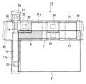
以上のように構成された各実施形態における液晶装置の全体構成を図7および図8を参照して説明する。なお、図7は、TFTアレイ基板をその上に形成された各構成要素とともに対向基板の側から見た平面図であり、図8は、図7のH−H’線に沿う断面図である。
【0064】
図7、図8において、TFTアレイ基板10は、上述した第1〜第3の実施の形態において説明したTFTアレイ基板である。TFTアレイ基板10の上には、シール材52がその縁に沿って設けられており、その内側に並行して、画像表示領域の周辺を規定する額縁としての遮光膜53が設けられている。シール材52の外側の領域には、データ線6aに画像信号を所定タイミングで供給することによりデータ線6aを駆動するデータ線駆動回路201および外部回路接続端子202がTFTアレイ基板10の一辺に沿って設けられており、走査線3aに走査信号を所定タイミングで供給することにより走査線3aを駆動する走査線駆動回路104が、この一辺に隣接する2辺に沿って設けられている。走査線3aに供給される走査信号遅延が問題にならないのならば、走査線駆動回路104は片側だけでも良いことは言うまでもない。また、データ線駆動回路201を画像表示領域10aの辺に沿って両側に配列してもよい。さらにTFTアレイ基板10Cの残る一辺には、画像表示領域の両側に設けられた走査線駆動回路104間をつなぐための複数の配線105が設けられている。
【0065】
また、対向基板20は、上述した第1の実施の形態において説明した対向基板であり、対向基板20のコーナー部の少なくとも1箇所においては、TFTアレイ基板10と対向基板20との間で電気的に導通をとるための導通材106が設けられている。そして、図8に示すように、図7に示したシール材52とほぼ同じ輪郭を持つ対向基板20が当該シール材52によりTFTアレイ基板10に固着されている。
【0066】
本実施の形態では、データ線駆動回路201および走査線駆動回路104を構成するTFT用のゲート線は、第1の実施の形態で説明した走査線3aを構成する層、データ線6aを構成する層、ゲート電極35を構成する層のいずれかを用いて構成することができる。つまり、これら駆動回路を構成するTFTに関しては、上述の画素スイッチング用TFTと同様の構成を採る必要がないため、走査線を構成する層、データ線を構成する層、ゲート電極を構成する層のいずれかを選んでゲート線を形成すればよい。
【0067】
なお、TFTアレイ基板10上には、これらのデータ線駆動回路201、走査線駆動回路104等に加えて、複数のデータ線6aに画像信号を所定のタイミングで印加するサンプリング回路、複数のデータ線6aに所定電圧レベルのプリチャージ信号を画像信号に先行して各々供給するプリチャージ回路、製造途中や出荷時の当該液晶装置の品質、欠陥等を検査するための検査回路等を形成してもよい。
【0068】
以上説明した実施の形態では、データ線駆動回路201および走査線駆動回路104をTFTアレイ基板10の上に設ける代わりに、例えばTAB(Tape Automated bonding)基板上に実装された駆動用LSIに、TFTアレイ基板10の周辺部に設けられた異方性導電フィルムを介して電気的および機械的に接続するようにしてもよい。
【0069】
[液晶装置の応用例]
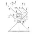
以上説明した各実施形態における液晶装置は、投射型表示装置(プロジェクタ)に適用できる。以下に、上述した液晶装置をライトバルブとして用いた液晶プロジェクタについて説明する。
【0070】
図9は、液晶プロジェクタの概略構成を示す図である。この図に示されるように、プロジェクタ1100内部には、ハロゲンランプ等の白色光源からなるランプユニット1102が設けられている。このランプユニット1102から射出された投射光は、内部に配置された3枚のミラー1106および2枚のダイクロイックミラー1108によってRGBの3原色に分離されて、各原色に対応するライトバルブ100R、100Gおよび100Bにそれぞれ導かれる。
【0071】
ここで、ライトバルブ100R、100Gおよび100Bの構成は、上述した実施の形態に係る液晶装置と同様であり、画像信号を入力する処理回路(図示省略)から供給されるR(赤)、G(緑)、B(青)の原色信号でそれぞれ駆動されるものである。また、B色の光は、他のR色やG色と比較すると、光路が長いので、その損失を防ぐために、入射レンズ1122、リレーレンズ1123および出射レンズ1124からなるリレーレンズ系1121を介して導かれる。
【0072】
ライトバルブ100R、100G、100Bによってそれぞれ変調された光は、ダイクロイックプリズム1112に3方向から入射する。そして、このダイクロイックプリズム1112において、R色およびB色の光は90度に屈折する一方、G色の光は直進する。したがって、各色の画像が合成された後、スクリーン1120には、投射レンズ1114によってカラー画像が投射されることとなる。
【0073】
なお、ライトバルブ100R、100Gおよび100Bには、ダイクロイックミラー1108によって、R、G、Bの各原色に対応する光が入射するので、上述したようにカラーフィルタを設ける必要はない。また、ライトバルブ100R、100Bの透過像はダイクロイックミラー1112により反射した後に投射されるのに対し、ライトバルブ100Gの透過像はそのまま投射されるので、ライトバルブ100R、100Bによる表示像を、ライトバルブ100Gによる表示像に対して左右反転させる構成となっている。
【0074】
なお、各実施形態では、対向基板にカラーフィルタは設けられていない。しかしながら、画素電極9に対向する所定領域に、RGBのカラーフィルタをその保護膜と共に対向基板上に形成してもよい。このようにすれば、プロジェクタ以外の直視型や反射型のカラー液晶装置について、各実施形態における液晶装置を適用できる。
また、対向基板上に1画素に対して1個のマイクロレンズを形成してもよい。あるいは、TFTアレイ基板上のRGBに対向する画素電極9の下にカラーレジスト等でカラーフィルタ層を形成することも可能である。このようにすれば、入射光の集光効率を向上することで、明るい液晶装置が実現できる。
さらにまた、対向基板上に、何層もの屈折率の相違する干渉層を堆積することで、光の干渉を利用して、RGB色を作り出すダイクロイックフィルタを形成してもよい。このダイクロイックフィルタ付き対向基板によれば、より明るいカラー液晶装置が実現できる。
【0075】
なお、本発明の技術範囲は上記実施の形態に限定されるものではなく、本発明の趣旨を逸脱しない範囲において種々の変更を加えることが可能である。例えば第1の実施の形態では、平坦な基板本体10A上にTFT素子30等を形成し、第1層間絶縁膜41で平坦化する例を挙げたが、第2層間絶縁膜で平坦化することもできる。その場合、ゲート線の膜厚のみで段差の設計を行うことができる。あるいは、基板本体10Aに格子状の溝を形成し、走査線3a、データ線6a、TFT素子30等の配線や素子をこの溝内に埋め込む構成としても良い。この場合には、配線、素子等が存在する領域と存在しない領域との間の段差が緩和され、この段差に起因した液晶の配向不良等の画像不良を低減することができる。また、パターン形状、断面構造、各膜の構成材料等に関する記載はほんの一例に過ぎず、適宜変更が可能である。また本発明は、例えば、エレクトロルミネッセンス(EL)、デジタルマイクロミラーデバイス(DMD)、あるいはプラズマ発光や電子放出による蛍光等を用いた様々な電気光学素子を用いた電気光学装置および該電気光学装置を備えた電子機器に対しても適用可能であることは言うまでもない。
【0076】
【発明の効果】
以上、詳細に説明したように、本発明によれば、走査線がデータ線と画素電極に平面的に重なっている部分が画素電極とデータ線とのカップリングを遮蔽するシールド層として機能するため、データ線の影響で画素電極の電位が変動するのが抑制され、フィールド反転駆動が可能になる。その結果、例えば高コントラスト、高開口率の液晶装置等の電気光学装置を実現することができる。
【図面の簡単な説明】
【図1】 本発明の第1の実施の形態の液晶装置の画像表示領域を構成するマトリクス状に形成された複数の画素における各種素子、配線等の等価回路である。
【図2】 同、液晶装置に用いるTFTアレイ基板(アクティブマトリクス基板)の1ドットのパターン構成を示す平面図である。
【図3】 図2のA−A’線に沿う断面図である。
【図4】 図2のB−B’線に沿う断面図である。
【図5】 本発明の第2の実施の形態の液晶装置に用いるTFTアレイ基板(アクティブマトリクス基板)の1ドットのパターン構成を示す平面図である。
【図6】 本発明の第2の実施の形態の液晶装置に用いるTFTアレイ基板(アクティブマトリクス基板)の1ドットのパターン構成を示す平面図である。
【図7】 本発明の液晶装置の全体構成を示す図であり、TFTアレイ基板をその上に形成された各構成要素とともに対向基板の側から見た平面図である。
【図8】 図7のH−H’線に沿う断面図である。
【図9】 本発明の電子機器の一例である液晶プロジェクタの概略構成を示す図である。
【符号の説明】
1 半導体層
3a 走査線
6a データ線
9 画素電極
10 TFTアレイ基板(アクティブマトリクス基板)
22 ゲートコンタクトホール
30 TFT素子(薄膜トランジスタ)
35 ゲート電極
45 下側遮光膜
47 中継導電膜
50 液晶層
70 保持容量
71 保持容量電極[0001]
BACKGROUND OF THE INVENTION
The present invention relates to an active matrix substrate, an electro-optical device, and an electronic apparatus, and more particularly to a configuration of an active matrix substrate suitable for use in a liquid crystal light valve mounted on a projection display device.
[0002]
[Prior art]
A liquid crystal light valve is known as a light modulation means mounted on a projection display device such as a liquid crystal projector. The liquid crystal light valve is mainly composed of a pair of substrates which are disposed to face each other with a liquid crystal layer interposed therebetween and which have electrodes for applying a voltage to the liquid crystal layer. In general, an active matrix type liquid crystal cell is used for a liquid crystal light valve, and higher definition of an image is being promoted.
[0003]
Conventionally, inversion driving methods such as dot inversion, line inversion, and field inversion have been adopted as driving methods for liquid crystal light valves in order to prevent burn-in and deterioration of the liquid crystal. Each of the above inversion driving methods has advantages and disadvantages. However, in the case of dot inversion or line inversion, a voltage of reverse polarity is applied to the pixel electrode of the adjacent dot, so that a horizontal electric field is generated between adjacent dots. There is a risk of light leakage due to disclination due to an electric field. As described above, since liquid crystal light valves are required to have high definition, this light leakage causes a decrease in contrast and a reduction in aperture ratio, which is a major factor in reducing display quality. Therefore, from this point of view, it is required to adopt a field inversion driving method that does not generate a horizontal electric field.
[0004]
[Problems to be solved by the invention]
However, the field inversion driving method cannot be adopted in the configuration of the conventional active matrix substrate. The reason is as follows.
In the field inversion driving, for example, when attention is paid to one data line, an image signal (voltage) having the same polarity is written in one field to all dots supplied with a signal from the data line. At the moment of moving to the next field, the polarity of the image signal supplied to the data line is reversed. At this time, if the scanning line side is scanned from the upper side to the lower side of the display area, the image signal supplied to the data line is immediately written in the upper dot of the display area, whereas the lower dot In FIG. 3, the pixel electrode holds the image signal written in the previous field, but the image line having the opposite polarity to the data line is present for a long time. Since the coupling between the pixel electrode and the data line occurs during this time, the potential of the pixel electrode fluctuates due to the influence of the data line in the dots on the lower side of the display area, and there is a problem that the display quality is deteriorated.
[0005]
The present invention has been made to solve the above-described problems, and is an electro-optical device such as a liquid crystal device capable of improving display quality by employing field inversion driving, an active matrix substrate used therefor, and an electronic device. The purpose is to provide equipment.
[0006]
[Means for Solving the Problems]
In order to achieve the above object, the active matrix substrate of the present invention is electrically connected to a plurality of data lines and a plurality of scanning lines provided on the substrate body so as to cross each other. An active matrix substrate comprising a plurality of thin film transistors and a plurality of pixel electrodes electrically connected to the plurality of thin film transistors, respectively, wherein the gate electrodes and the scanning lines constituting the thin film transistors are different from each other. A layer that is electrically connected via a contact hole that penetrates an interlayer insulating film between the gate electrode and the scanning line, and the layer that constitutes the scanning line constitutes the data line Located above the layer and below the layer constituting the pixel electrode, the scanning line pattern, the data line pattern, and the The pattern of the pixel electrode, characterized in that the partially overlapped in plan view.
[0007]
That is, the active matrix substrate of the present invention does not have a structure in which a gate electrode constituting a thin film transistor (hereinafter abbreviated as TFT) is formed integrally with a scanning line, and the gate electrode is different from the scanning line. The gate electrode and the scanning line are electrically connected through a contact hole. As a cross-sectional structure, the layer constituting the scanning line is located between the layer constituting the data line and the layer constituting the pixel electrode, and in a plan view, the scanning line pattern is the data line pattern. And partially overlaps the pixel electrode pattern. From such a structure, the portion where the scanning line overlaps the data line and the pixel electrode shields the “coupling between the pixel electrode and the data line” described in the section “Problems to be solved by the invention”. Functions as a shield layer. Therefore, a phenomenon in which the potential of the pixel electrode fluctuates due to the influence of the data line hardly occurs in any part of the display area, and the electro-optical device using the active matrix substrate can perform field inversion driving. As a result of employing the field inversion drive, for example, an electro-optical device such as a liquid crystal device having a high contrast and a high aperture ratio can be obtained. Further, since the scanning lines necessary for the active matrix substrate are used as the shield layer, and a separate pattern that functions only as the shield layer is not added, the pattern configuration is not particularly complicated.
[0008]
In the active matrix substrate of the present invention, it is preferable that the scanning line is formed of a material containing metal. Further, the data line is preferably formed of a material containing metal. “Metal-containing material” means that it may be composed of a single metal layer or a laminated film including a metal film.
[0009]
For example, a liquid crystal device mounted as a light modulation unit in a projection display device is irradiated with much stronger light than, for example, a direct-view liquid crystal display having a backlight. At this time, if a TFT provided as a pixel switching element is irradiated with light, a light leakage current flows between the source and drain regions, resulting in degradation of TFT characteristics, or in an extreme case, malfunction. There's a problem. Therefore, a light shielding film has been conventionally formed on an active matrix substrate, and a light shielding film is formed separately from various wirings, and in order to simplify the substrate configuration, for example, WSi (highly light shielding property) Conventionally, a scanning line is formed of a material such as tungsten silicide, and this is used as a light shielding film and scanning line. However, especially in the latter case, a material such as WSi is excellent in light-shielding properties, but the sheet resistance is as high as about 5Ω, and the display quality is deteriorated due to the signal delay of the scanning line. Furthermore, since the light shielding film is disposed only in one direction, the light leakage current is not sufficiently suppressed.
[0010]
On the other hand, in the active matrix substrate of the present invention, if the scanning line is made of a metal-containing material, for example, aluminum, the sheet resistance is about 0.1Ω, which is sufficiently smaller than the above WSi, so that the frequency of 60 Hz or more. Even when driven at a high frequency, a reduction in display quality due to a signal delay of the scanning line can be suppressed. Similarly, if the data line is formed of a material containing metal, it is possible to suppress deterioration in display quality due to signal delay of the data line. In particular, if both the scanning line and the data line are formed of a material containing metal, the scanning line and the data line function as a light shielding film, and the light shielding film is arranged in a lattice shape. Can be suppressed.
[0011]
Various materials can be used for the gate electrode, but it is preferable that the gate electrode be formed of polycrystalline silicon.
[0012]
In the case where the scanning line and the gate electrode have an integrated structure, when the scanning line is formed of metal, the gate electrode naturally becomes metal. However, if the gate electrode is formed of a metal, the metal may diffuse into the gate insulating film due to, for example, a heat treatment step in the manufacturing process, which may cause problems such as unstable TFT device characteristics. Therefore, in the active matrix substrate of the present invention, since the scanning lines and the gate electrodes are formed in different layers, both constituent materials can be individually selected, and the scanning lines are made of metal to prevent wiring delay. The gate electrode can be formed of polycrystalline silicon. As a result, the element characteristics of the TFT can be stabilized and the reliability can be improved.
[0013]
It is desirable to provide a light shielding film extending in a lattice shape in the direction along the scanning lines and the data lines via an interlayer insulating film below the semiconductor layer constituting the channel region of the TFT.
[0014]
As described above, when the scanning lines and the data lines are formed of a metal having a high light shielding property, the scanning lines and the data lines function as a light shielding film, and can prevent light from entering the TFT from above the substrate. In addition, when a light-shielding film extending in a lattice shape in the direction along the scanning lines and data lines is provided below the semiconductor layer constituting the channel region of the TFT, it can prevent light from entering the TFT from below the substrate. it can.
[0015]
Further, a storage capacitor electrode that forms a storage capacitor with a semiconductor layer that forms the channel region of the TFT is provided, and the storage capacitor electrode is formed of the same layer as that that forms the gate electrode. Good.
[0016]
According to this configuration, the image signal (voltage) written to the pixel electrode can be held more reliably, and can be performed simultaneously with the formation of the gate electrode when forming the storage capacitor electrode constituting the storage capacitor. The process is not complicated.
[0017]
Further, when the storage capacitor electrode and the light shielding film (light shielding film under the semiconductor layer) are provided, the storage capacitor electrode and the light shielding film pass through the interlayer insulating film between the storage capacitor electrode and the light shielding film. It is desirable that they are electrically connected via each other.
[0018]
According to this configuration, since the storage capacitor electrode and the light shielding film have a common potential and are positioned above and below the semiconductor layer of the TFT via the interlayer insulating film, the storage capacitor is stacked in two stages above and below the semiconductor layer. Can be formed. As a result, it is possible to increase the storage capacity value in a certain occupied area, and to improve display quality. Alternatively, the area occupied by the storage capacitor can be reduced in order to obtain a certain storage capacitor value, and the aperture ratio can be increased. Further, since the potential of the light shielding film located below the TFT can be fixed, the operational stability of the TFT can be improved.
[0019]
The scanning line may have a portion protruding from the main scanning line along the data line. Similarly, the data line may have a portion protruding from the data line main line along the scanning line.
[0020]
According to this configuration, the portion branched from the scanning line main line or the data line main line and projecting in the vertical direction can constitute a part of the light shielding film, and the light shielding property for the TFT can be further improved.
[0021]
A relay conductive film formed of the same layer as the data line may be provided, and the semiconductor layer and the pixel electrode may be electrically connected via the relay conductive film. For example, when the pixel electrode is made of a transparent conductive film such as indium tin oxide (hereinafter abbreviated as ITO), at least the upper surface of the relay conductive film is made of a material that can form an ohmic contact with the transparent conductive film. It is desirable that
[0022]
According to this configuration, by providing the relay conductive film, even if the interlayer distance between the semiconductor layer and the pixel electrode is as long as about 1 to 2 μm, for example, it is technically difficult to connect them with one contact hole. While avoiding this, two or more contact holes having a relatively small diameter can be connected to each other satisfactorily, and the pixel aperture ratio can be increased. In general, a semiconductor layer constituting a TFT is very thin, but it is also useful for preventing etching through when a contact hole is opened. In particular, if at least the upper surface of the relay conductive film is made of a material that can form ohmic contact with the transparent conductive film, the contact resistance can be reduced.
[0023]
Further, a driving circuit for driving the scanning line or the data line is provided, and the gate line for the TFT constituting the driving circuit constitutes the layer constituting the scanning line, the layer constituting the data line, and the gate electrode. Any of the layers can be used.
[0024]
In the TFT corresponding to each dot in the display region, the scanning line and the gate electrode need to be formed in different layers and electrically connected through the contact hole in order to achieve the above-described effect of the present invention. On the other hand, when a drive circuit is provided on the active matrix substrate, there are no particular restrictions on the TFTs that make up the drive circuit, so the layers that make up the scan lines, the layers that make up the data lines, and the gate electrodes A gate line may be formed by selecting any of the constituent layers.
[0025]
In addition, it is desirable that the upper surface of the scanning line or data line formation region is located higher than the upper surface of the central portion of the pixel electrode formation region.
[0026]
As described above, disclination occurs at the boundary between adjacent dots, and there is a risk of light leakage. On the other hand, with the above configuration, the scanning line or data line forming region, that is, the peripheral portion of each dot is shaped like a bank, and the liquid crystal layer thickness of this part is the central portion of the pixel electrode forming region. That is, since the thickness of the liquid crystal layer at the center of each dot is thinner, the strength of the vertical electric field applied to the liquid crystal layer is increased at the periphery of the dot, and the effect of reducing disclination is obtained.
[0027]
When the above configuration is employed, a configuration in which the upper surface of the interlayer insulating film in contact with the data line below the data line is planarized may be employed. Alternatively, the upper surface of the interlayer insulating film in contact with the scan line may be planarized below the scan line.
[0028]
As described above, when the periphery of the dot is shaped like a bank, if the upper surface of the interlayer insulating film in contact with the data line is flattened below the data line, the data line and scanning line films The height of the bank can be adjusted by the thickness, and disclination can be reliably suppressed. Further, when the upper surface of the interlayer insulating film in contact with the scanning line is planarized below the scanning line, the height of the bank can be adjusted only by the film thickness of the scanning line.
[0029]
Or you may provide a recessed part in the formation area of TFT of a board | substrate body.
According to this configuration, a part of the TFT can be embedded in the concave portion of the substrate body, and the upper surface of the active matrix substrate can be flattened contrary to the above case.
[0030]
An electro-optical device according to the present invention includes the active matrix substrate according to the present invention.
[0031]
According to this configuration, since the field inversion driving can be adopted by providing the active matrix substrate of the present invention, an electro-optical device such as a liquid crystal device having a high contrast and a high aperture ratio can be obtained.
[0032]
An electronic apparatus according to the present invention includes the electro-optical device according to the present invention. According to this configuration, it is possible to realize an electronic device including a display unit with excellent display quality.
[0033]
DETAILED DESCRIPTION OF THE INVENTION
[First Embodiment]
A first embodiment of the present invention will be described below with reference to FIGS.
In this embodiment, a liquid crystal device (liquid crystal light valve) mounted on a projection display device will be described as an example of an electro-optical device using the active matrix substrate of the present invention.
[0034]
FIG. 1 is an equivalent circuit of various elements, wirings, and the like in a plurality of pixels formed in a matrix that forms an image display area of a liquid crystal device. FIG. 2 is a plan view showing a 1-dot pattern configuration of a TFT array substrate (active matrix substrate) on which data lines, scanning lines, pixel electrodes and the like are formed. 3 is a cross-sectional view taken along the line AA ′ in FIG. 2, and FIG. 4 is a cross-sectional view taken along the line BB ′ in FIG. In addition, in each figure, in order to make each layer and each member the size which can be recognized on drawing, the scale is varied for every layer and each member.
[0035]
In FIG. 1, each of a plurality of dots formed in a matrix that forms an image display area of the liquid crystal device according to the present embodiment has a
[0036]
Further, the
[0037]
Here, in order to prevent the held image signal from leaking, a holding
[0038]
As shown in FIG. 2, a
[0039]
The
[0040]
A
[0041]
The relay
[0042]
As shown in FIGS. 3 and 4, the liquid crystal device according to the present embodiment includes a
[0043]
In the
[0044]
As shown in FIG. 3, in the case of the present embodiment, the pixel switching
[0045]
A
[0046]
As shown in FIGS. 3 and 4, a first
[0047]
A second
[0048]
As shown in FIG. 4, an
[0049]
On the other hand, with respect to the configuration on the
[0050]
In the present embodiment, the
[0051]
Further, since the
[0052]
In the present embodiment, since the
[0053]
A lower light-shielding
[0054]
In the configuration of the present embodiment, the high-
[0055]
Further, since the peripheral edge of the dot has a bank-like shape and the liquid crystal layer thickness of this part is thinner than the liquid crystal layer thickness of the central part of the dot, the vertical electric field (liquid crystal The strength of the electric field in the cell thickness direction is increased, the disclination that tends to occur at the periphery of the dot is reduced, and the effect of suppressing light leakage is obtained. In this embodiment, since the upper surface of the first
[0056]
In the liquid crystal device according to the present embodiment, the pixel switching
[0057]
[Second Embodiment]
The second embodiment of the present invention will be described below with reference to FIG.
The basic configuration of the liquid crystal device of the present embodiment is the same as that of the first embodiment, and only the plane pattern is slightly different. Accordingly, only the plane pattern will be described with reference to FIG. 5 (a plan view corresponding to FIG. 2 of the first embodiment, and the same components as those in FIG. Omitted.
[0058]
In the first embodiment, the
[0059]
In the case of the present embodiment, the
[0060]
[Third Embodiment]
The third embodiment of the present invention will be described below with reference to FIG.
The basic configuration of the liquid crystal device of the present embodiment is the same as that of the first embodiment, and only the plane pattern is slightly different. Therefore, only the plane pattern will be described with reference to FIG. 6 (a plan view corresponding to FIG. 2 of the first embodiment, and the same components as those in FIG. Omitted.
[0061]
In the first embodiment, the
[0062]
In the case of this embodiment, the pattern shape of each layer is substantially the same as in the first embodiment. However, since the
[0063]
[Overall configuration of liquid crystal device]
The overall configuration of the liquid crystal device in each embodiment configured as described above will be described with reference to FIGS. 7 is a plan view of the TFT array substrate viewed from the side of the counter substrate together with the components formed thereon, and FIG. 8 is a cross-sectional view taken along the line HH ′ of FIG. .
[0064]
7 and 8, the
[0065]
The
[0066]
In the present embodiment, the gate lines for TFTs constituting the data
[0067]
On the
[0068]
In the embodiment described above, instead of providing the data line driving
[0069]
[Application examples of liquid crystal devices]
The liquid crystal device in each of the embodiments described above can be applied to a projection display device (projector). A liquid crystal projector using the above-described liquid crystal device as a light valve will be described below.
[0070]
FIG. 9 is a diagram showing a schematic configuration of the liquid crystal projector. As shown in this figure, a
[0071]
Here, the configuration of the
[0072]
The lights modulated by the
[0073]
Since light corresponding to the primary colors R, G, and B is incident on the
[0074]
In each embodiment, no color filter is provided on the counter substrate. However, an RGB color filter may be formed on a counter substrate together with its protective film in a predetermined region facing the
One microlens may be formed for one pixel on the counter substrate. Alternatively, it is possible to form a color filter layer with a color resist or the like under the
Furthermore, a dichroic filter that creates RGB colors by using interference of light may be formed by depositing several layers of interference layers having different refractive indexes on the counter substrate. According to this counter substrate with a dichroic filter, a brighter color liquid crystal device can be realized.
[0075]
The technical scope of the present invention is not limited to the above embodiment, and various modifications can be made without departing from the spirit of the present invention. For example, in the first embodiment, an example in which the
[0076]
【The invention's effect】
As described above in detail, according to the present invention, the portion where the scanning line overlaps the data line and the pixel electrode in a plane functions as a shield layer that shields the coupling between the pixel electrode and the data line. The fluctuation of the potential of the pixel electrode due to the influence of the data line is suppressed, and the field inversion driving is enabled. As a result, an electro-optical device such as a liquid crystal device having a high contrast and a high aperture ratio can be realized.
[Brief description of the drawings]
FIG. 1 is an equivalent circuit of various elements, wirings, and the like in a plurality of pixels formed in a matrix that forms an image display region of a liquid crystal device according to a first embodiment of the present invention.
FIG. 2 is a plan view showing a 1-dot pattern configuration of a TFT array substrate (active matrix substrate) used in the liquid crystal device.
FIG. 3 is a cross-sectional view taken along the line AA ′ of FIG.
4 is a cross-sectional view taken along line BB ′ of FIG.
FIG. 5 is a plan view showing a 1-dot pattern configuration of a TFT array substrate (active matrix substrate) used in a liquid crystal device according to a second embodiment of the present invention.
FIG. 6 is a plan view showing a 1-dot pattern configuration of a TFT array substrate (active matrix substrate) used in a liquid crystal device according to a second embodiment of the present invention.
FIG. 7 is a diagram showing an overall configuration of a liquid crystal device of the present invention, and is a plan view of a TFT array substrate together with each component formed thereon, as viewed from the counter substrate side.
8 is a cross-sectional view taken along the line HH ′ of FIG.
FIG. 9 is a diagram showing a schematic configuration of a liquid crystal projector which is an example of the electronic apparatus of the invention.
[Explanation of symbols]
1 Semiconductor layer
3a scanning line
6a Data line
9 Pixel electrode
10 TFT array substrate (active matrix substrate)
22 Gate contact hole
30 TFT elements (thin film transistors)
35 Gate electrode
45 Lower light shielding film
47 Relay conductive film
50 Liquid crystal layer
70 holding capacity
71 Retention capacitance electrode
Claims (18)
Translated fromJapanese前記薄膜トランジスタを構成するゲート電極と前記走査線とが別の層で構成されるとともに、前記ゲート電極と前記走査線との間の層間絶縁膜を貫通するコンタクトホールを介して電気的に接続され、
前記走査線を構成する層が、前記データ線を構成する層よりも上層側かつ前記画素電極を構成する層よりも下層側に位置し、前記走査線のパターンと前記データ線のパターンと前記画素電極のパターンとが平面的に一部重なっていることを特徴とするアクティブマトリクス基板。A plurality of data lines and a plurality of scanning lines provided on the substrate body so as to intersect with each other, a plurality of thin film transistors electrically connected to the data lines and the scanning lines, and a plurality of thin film transistors electrically connected to the plurality of thin film transistors, respectively. An active matrix substrate including a plurality of pixel electrodes,
The gate electrode constituting the thin film transistor and the scanning line are constituted by different layers, and are electrically connected via a contact hole penetrating an interlayer insulating film between the gate electrode and the scanning line,
The layer constituting the scanning line is located above the layer constituting the data line and on the lower layer side than the layer constituting the pixel electrode, and the scanning line pattern, the data line pattern, and the pixel An active matrix substrate, wherein an electrode pattern partially overlaps with a plane.
Priority Applications (5)
| Application Number | Priority Date | Filing Date | Title |
|---|---|---|---|
| JP2002212762AJP3661669B2 (en) | 2002-07-22 | 2002-07-22 | Active matrix substrate, electro-optical device, electronic equipment |
| US10/614,868US6836302B2 (en) | 2002-07-22 | 2003-07-09 | Active matrix substrate, electro-optical device and electronic equipment |
| TW092119589ATWI247257B (en) | 2002-07-22 | 2003-07-17 | Active matrix substrate, photoelectric device and electronic device |
| CNB031328172ACN1238756C (en) | 2002-07-22 | 2003-07-21 | Active matrix substrate, photoelectric device and electronic device |
| KR1020030049686AKR100687987B1 (en) | 2002-07-22 | 2003-07-21 | Active matrix substrates, electro-optical devices, electronic devices |
Applications Claiming Priority (1)
| Application Number | Priority Date | Filing Date | Title |
|---|---|---|---|
| JP2002212762AJP3661669B2 (en) | 2002-07-22 | 2002-07-22 | Active matrix substrate, electro-optical device, electronic equipment |
Publications (2)
| Publication Number | Publication Date |
|---|---|
| JP2004054033A JP2004054033A (en) | 2004-02-19 |
| JP3661669B2true JP3661669B2 (en) | 2005-06-15 |
Family
ID=31492064
Family Applications (1)
| Application Number | Title | Priority Date | Filing Date |
|---|---|---|---|
| JP2002212762AExpired - Fee RelatedJP3661669B2 (en) | 2002-07-22 | 2002-07-22 | Active matrix substrate, electro-optical device, electronic equipment |
Country Status (5)
| Country | Link |
|---|---|
| US (1) | US6836302B2 (en) |
| JP (1) | JP3661669B2 (en) |
| KR (1) | KR100687987B1 (en) |
| CN (1) | CN1238756C (en) |
| TW (1) | TWI247257B (en) |
Families Citing this family (22)
| Publication number | Priority date | Publication date | Assignee | Title |
|---|---|---|---|---|
| JP2004151546A (en)* | 2002-10-31 | 2004-05-27 | Sharp Corp | Active matrix substrate and display device |
| JP4055764B2 (en)* | 2004-01-26 | 2008-03-05 | セイコーエプソン株式会社 | Electro-optical device and electronic apparatus |
| JP2006154563A (en)* | 2004-11-30 | 2006-06-15 | Victor Co Of Japan Ltd | Reflection type liquid crystal display device |
| US8053777B2 (en)* | 2005-03-31 | 2011-11-08 | General Electric Company | Thin film transistors for imaging system and method of making the same |
| KR100754128B1 (en)* | 2005-11-23 | 2007-08-30 | 삼성에스디아이 주식회사 | LCD array substrate and manufacturing method thereof |
| US8223287B2 (en)* | 2006-10-11 | 2012-07-17 | Seiko Epson Corporation | Electrooptic device and electronic device |
| CN100426504C (en)* | 2006-11-06 | 2008-10-15 | 北京京东方光电科技有限公司 | Single grid double tunnel pixel |
| JP4225347B2 (en)* | 2006-12-15 | 2009-02-18 | セイコーエプソン株式会社 | Electro-optical device and electronic apparatus |
| JP2008233399A (en)* | 2007-03-19 | 2008-10-02 | Sony Corp | Pixel circuit, display device, and manufacturing method of display device |
| JP2009059894A (en)* | 2007-08-31 | 2009-03-19 | Oki Electric Ind Co Ltd | Semiconductor device |
| JP2009187825A (en)* | 2008-02-07 | 2009-08-20 | Canon Inc | Manufacturing method of image display device |
| JP5098682B2 (en)* | 2008-02-15 | 2012-12-12 | セイコーエプソン株式会社 | ELECTRO-OPTICAL DEVICE, MANUFACTURING METHOD THEREOF, AND ELECTRONIC DEVICE |
| US9280025B2 (en)* | 2009-03-18 | 2016-03-08 | Unified Innovative Technology, Llc | Active matrix substrate and display device |
| CN102269900B (en)* | 2010-06-03 | 2013-04-24 | 北京京东方光电科技有限公司 | Thin film transistor (TFT) array substrate and making method thereof |
| CN102176095B (en)* | 2011-02-24 | 2014-04-02 | 华映视讯(吴江)有限公司 | Film transistor substrate of liquid crystal display (LCD) panel |
| CN103489824B (en)* | 2013-09-05 | 2016-08-17 | 京东方科技集团股份有限公司 | A kind of array base palte and preparation method thereof and display device |
| CN104199205B (en)* | 2014-08-27 | 2016-08-31 | 京东方科技集团股份有限公司 | A kind of display device |
| CN107845648A (en)* | 2017-10-31 | 2018-03-27 | 上海天马有机发光显示技术有限公司 | A kind of array base palte, organic electroluminescence display panel and display device |
| JP6597768B2 (en) | 2017-12-27 | 2019-10-30 | セイコーエプソン株式会社 | Electro-optical device and electronic apparatus |
| JP6566079B1 (en) | 2018-04-25 | 2019-08-28 | セイコーエプソン株式会社 | Electro-optical device, electronic equipment |
| JP7471075B2 (en)* | 2019-12-17 | 2024-04-19 | シャープ株式会社 | Active matrix substrate and its manufacturing method |
| CN111754934A (en) | 2020-06-22 | 2020-10-09 | 武汉华星光电半导体显示技术有限公司 | Display panel and display device |
Family Cites Families (4)
| Publication number | Priority date | Publication date | Assignee | Title |
|---|---|---|---|---|
| JP3796072B2 (en)* | 1999-08-04 | 2006-07-12 | シャープ株式会社 | Transmission type liquid crystal display device |
| KR100481590B1 (en)* | 2000-04-21 | 2005-04-08 | 세이코 엡슨 가부시키가이샤 | Electrooptic device, projection type display and method for manufacturing electrooptic device |
| TW466773B (en)* | 2000-12-15 | 2001-12-01 | Acer Display Tech Inc | Manufacturing method of thin film transistor liquid crystal display |
| US7167217B2 (en)* | 2002-08-23 | 2007-01-23 | Lg.Philips Lcd Co., Ltd. | Liquid crystal display device and method for manufacturing the same |
- 2002
- 2002-07-22JPJP2002212762Apatent/JP3661669B2/ennot_activeExpired - Fee Related
- 2003
- 2003-07-09USUS10/614,868patent/US6836302B2/ennot_activeExpired - Fee Related
- 2003-07-17TWTW092119589Apatent/TWI247257B/ennot_activeIP Right Cessation
- 2003-07-21CNCNB031328172Apatent/CN1238756C/ennot_activeExpired - Fee Related
- 2003-07-21KRKR1020030049686Apatent/KR100687987B1/ennot_activeExpired - Fee Related
Also Published As
| Publication number | Publication date |
|---|---|
| CN1238756C (en) | 2006-01-25 |
| KR100687987B1 (en) | 2007-02-27 |
| US20040051822A1 (en) | 2004-03-18 |
| KR20040010285A (en) | 2004-01-31 |
| TWI247257B (en) | 2006-01-11 |
| TW200411607A (en) | 2004-07-01 |
| CN1474219A (en) | 2004-02-11 |
| JP2004054033A (en) | 2004-02-19 |
| US6836302B2 (en) | 2004-12-28 |
Similar Documents
| Publication | Publication Date | Title |
|---|---|---|
| JP3661669B2 (en) | Active matrix substrate, electro-optical device, electronic equipment | |
| JP3700697B2 (en) | Electro-optical device and electronic apparatus | |
| JP3870897B2 (en) | Electro-optical device and electronic apparatus | |
| KR100614737B1 (en) | Electro-optical devices and electronic devices | |
| JP2002108248A (en) | Electro-optical device, substrate for electro-optical device, and projection display device | |
| JP2004342923A (en) | Liquid crystal device, active matrix substrate, display device, and electronic device | |
| US7561220B2 (en) | Electro-optical device and manufacturing method thereof, electronic apparatus, and capacitor | |
| TWI274309B (en) | Electro-optical device and electronic machine | |
| JP3821067B2 (en) | Electro-optical device and electronic apparatus | |
| JP3608531B2 (en) | Electro-optical device and projection display device | |
| KR100568372B1 (en) | Electro-optical devices and electronic devices | |
| JP2018136477A (en) | Electro-optical device, electronic equipment | |
| JP2003280020A (en) | Electro-optical device, method of manufacturing the same, and electronic apparatus | |
| JP3849434B2 (en) | Electro-optical device and projection display device | |
| JP4023522B2 (en) | Electro-optical device and projector | |
| JP2003337553A (en) | Electro-optical devices and electronic equipment | |
| JP2004109988A (en) | Electro-optical devices and electronic equipment | |
| JP2001305581A (en) | Electro-optical device | |
| US7667681B2 (en) | Electro-optical device having exterior circuit connection terminal | |
| JP4063260B2 (en) | Electro-optical device and projection display device | |
| JP4026398B2 (en) | Electro-optical device and electronic apparatus | |
| JP3729071B2 (en) | Electro-optical device and projector | |
| JP2011221119A (en) | Electro-optic device, electronic equipment, and manufacturing method of electro-optic device | |
| JP5176852B2 (en) | Electro-optical device and electronic apparatus | |
| JP3925555B2 (en) | Electro-optical device and electronic apparatus |
Legal Events
| Date | Code | Title | Description |
|---|---|---|---|
| A977 | Report on retrieval | Free format text:JAPANESE INTERMEDIATE CODE: A971007 Effective date:20050118 | |
| TRDD | Decision of grant or rejection written | ||
| A01 | Written decision to grant a patent or to grant a registration (utility model) | Free format text:JAPANESE INTERMEDIATE CODE: A01 Effective date:20050301 | |
| A61 | First payment of annual fees (during grant procedure) | Free format text:JAPANESE INTERMEDIATE CODE: A61 Effective date:20050314 | |
| R150 | Certificate of patent or registration of utility model | Free format text:JAPANESE INTERMEDIATE CODE: R150 | |
| FPAY | Renewal fee payment (event date is renewal date of database) | Free format text:PAYMENT UNTIL: 20080401 Year of fee payment:3 | |
| FPAY | Renewal fee payment (event date is renewal date of database) | Free format text:PAYMENT UNTIL: 20090401 Year of fee payment:4 | |
| FPAY | Renewal fee payment (event date is renewal date of database) | Free format text:PAYMENT UNTIL: 20090401 Year of fee payment:4 | |
| FPAY | Renewal fee payment (event date is renewal date of database) | Free format text:PAYMENT UNTIL: 20100401 Year of fee payment:5 | |
| FPAY | Renewal fee payment (event date is renewal date of database) | Free format text:PAYMENT UNTIL: 20110401 Year of fee payment:6 | |
| FPAY | Renewal fee payment (event date is renewal date of database) | Free format text:PAYMENT UNTIL: 20110401 Year of fee payment:6 | |
| FPAY | Renewal fee payment (event date is renewal date of database) | Free format text:PAYMENT UNTIL: 20120401 Year of fee payment:7 | |
| FPAY | Renewal fee payment (event date is renewal date of database) | Free format text:PAYMENT UNTIL: 20130401 Year of fee payment:8 | |
| LAPS | Cancellation because of no payment of annual fees |