JP3661149B2 - Contact module - Google Patents
Contact moduleDownload PDFInfo
- Publication number
- JP3661149B2 JP3661149B2JP2002300467AJP2002300467AJP3661149B2JP 3661149 B2JP3661149 B2JP 3661149B2JP 2002300467 AJP2002300467 AJP 2002300467AJP 2002300467 AJP2002300467 AJP 2002300467AJP 3661149 B2JP3661149 B2JP 3661149B2
- Authority
- JP
- Japan
- Prior art keywords
- contact
- insulator
- view
- contact module
- contacts
- Prior art date
- Legal status (The legal status is an assumption and is not a legal conclusion. Google has not performed a legal analysis and makes no representation as to the accuracy of the status listed.)
- Expired - Fee Related
Links
- 239000012212insulatorSubstances0.000claimsdescription41
- 238000000034methodMethods0.000description22
- 238000002788crimpingMethods0.000description13
- 239000011347resinSubstances0.000description10
- 229920005989resinPolymers0.000description10
- 238000007796conventional methodMethods0.000description6
- 238000004519manufacturing processMethods0.000description4
- 238000000465mouldingMethods0.000description4
- 239000000758substrateSubstances0.000description2
- 238000010586diagramMethods0.000description1
- 238000010438heat treatmentMethods0.000description1
- 239000011810insulating materialSubstances0.000description1
- 239000002184metalSubstances0.000description1
- 125000006850spacer groupChemical group0.000description1
Images


Classifications
- H—ELECTRICITY
- H01—ELECTRIC ELEMENTS
- H01R—ELECTRICALLY-CONDUCTIVE CONNECTIONS; STRUCTURAL ASSOCIATIONS OF A PLURALITY OF MUTUALLY-INSULATED ELECTRICAL CONNECTING ELEMENTS; COUPLING DEVICES; CURRENT COLLECTORS
- H01R13/00—Details of coupling devices of the kinds covered by groups H01R12/70 or H01R24/00 - H01R33/00
- H01R13/40—Securing contact members in or to a base or case; Insulating of contact members
- H01R13/405—Securing in non-demountable manner, e.g. moulding, riveting
- H01R13/41—Securing in non-demountable manner, e.g. moulding, riveting by frictional grip in grommet, panel or base
- H—ELECTRICITY
- H01—ELECTRIC ELEMENTS
- H01R—ELECTRICALLY-CONDUCTIVE CONNECTIONS; STRUCTURAL ASSOCIATIONS OF A PLURALITY OF MUTUALLY-INSULATED ELECTRICAL CONNECTING ELEMENTS; COUPLING DEVICES; CURRENT COLLECTORS
- H01R12/00—Structural associations of a plurality of mutually-insulated electrical connecting elements, specially adapted for printed circuits, e.g. printed circuit boards [PCB], flat or ribbon cables, or like generally planar structures, e.g. terminal strips, terminal blocks; Coupling devices specially adapted for printed circuits, flat or ribbon cables, or like generally planar structures; Terminals specially adapted for contact with, or insertion into, printed circuits, flat or ribbon cables, or like generally planar structures
- H01R12/70—Coupling devices
- H01R12/71—Coupling devices for rigid printing circuits or like structures
- H01R12/72—Coupling devices for rigid printing circuits or like structures coupling with the edge of the rigid printed circuits or like structures
- H01R12/722—Coupling devices for rigid printing circuits or like structures coupling with the edge of the rigid printed circuits or like structures coupling devices mounted on the edge of the printed circuits
- H01R12/724—Coupling devices for rigid printing circuits or like structures coupling with the edge of the rigid printed circuits or like structures coupling devices mounted on the edge of the printed circuits containing contact members forming a right angle
Landscapes
- Connector Housings Or Holding Contact Members (AREA)
- Details Of Connecting Devices For Male And Female Coupling (AREA)
- Coupling Device And Connection With Printed Circuit (AREA)
Description
Translated fromJapanese【0001】
【発明の属する技術分野】
本発明は、コネクタにおいて、インシュレータと、インシュレータに保持される複数のコンタクトとから構成されるコンタクトモジュールに関する。
【0002】
【従来の技術】
相互に直交する2枚の基板の間を電気的に接続するコネクタにおいて、インシュレータにコンタクトを保持する方法としては、一般にインサート成形による方法(以下「第1の従来の技術」という。)や別個の部品を採用する方法(以下「第2の従来の技術」という。)が、知られている。
【0003】
第1の従来の技術は、1枚の金属板からプレス加工によって打ち抜かれたリードフレーム(複数本のコンタクトを一体に有する。)をインシュレータにモールドする方法である(例えば、特許文献1参照。)。
【0004】
第2の従来の技術については、図9を参照して説明する。
【0005】
コンタクトモジュール31は、4本のコンタクト32と、一方の樹脂モールド部材33と、他方の樹脂モールド部材34とから構成される。
【0006】
各コンタクト32は、90゜のアングル形状に折曲され、それぞれの長さが異なる。一方の樹脂モールド部材33には、各コンタクト32をそれぞれ収納するための溝33aが形成される。他方の樹脂モールド部材34の一端側には、直角方向に突起部34aが形成される。突起部34aは、このコンタクトモジュール31が他のコンタクトモジュールと隣接するときのスペーサの役割を果す。
【0007】
各コンタクト32を一方の樹脂モールド部材33の各溝33aに矢印方向に収納した後、他方の樹脂モールド部材34を矢印方向に一方の樹脂モールド部材33に重畳する。すると、各コンタクト32は、両樹脂モールド部材33,34によって挟持されて組み付けられる。また、数組の両樹脂モールド部材33,34は、一括してロケータ(図示せず)によって離間しないように保持される(例えば、特許文献2参照。)。
【0008】
【特許文献1】
特許第2537698号公報(第3頁第5欄第42行−第6欄第28行、第5図−第8図)
【0009】
【特許文献2】
特開2000−113928号公報(第3頁第4欄第38行−第4頁第5欄第10行、図1)
【0010】
【発明が解決しようとする課題】
第1の従来の技術では、リードフレームをインシュレータにインサート成形するために、高価な金型を必要とし、また、コンタクトモジュールの製造工程が煩雑である。
【0011】
第2の従来の技術では、別個の部品(他方の樹脂モールド部材34)を必要とし、また、その製造用の高価な金型も必要とし、更に、コンタクトモジュールの組立工程が複雑である。
【0012】
そこで、本発明は、前記両従来の技術の欠点を改良し、インサート成形用金型も別個の部品及びその製造用金型も不要で、組立部品点数が少なく、しかも、コストが安価なコンタクトモジュールを提供しようとするものである。
【0013】
【課題を解決するための手段】
本発明は、前記課題を解決するため、次の手段を採用する。
【0014】
1.複数のコンタクトと、前記各コンタクトを保持するインシュレータとから構成されるコンタクトモジュールにおいて、前記各コンタクトは、接触部、端子部、前記接触部と前記端子部との間を連結する中間部、及び、被位置決め部を有し、前記インシュレータは、前記各コンタクトをそれぞれ収納する複数の溝、複数の位置決め部、及び、複数のカシメ部を有し、前記各被位置決め部と前記各位置決め部とが係合することによって、前記各コンタクトが前記インシュレータに位置決めされ、かつ、前記各カシメ部を変形することによって、前記各コンタクトが前記インシュレータに固定されるコンタクトモジュール。
【0015】
2.前記各被位置決め部を前記各位置決め部に圧入することによって、前記各コンタクトが前記インシュレータに仮保持される前記1記載のコンタクトモジュール。
【0016】
【発明の実施の形態】
本発明の一実施の形態例のコンタクトモジュールについて図1〜図8を参照して説明する。
【0017】
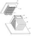
図1は、バックプレーン1に圧入によって取付けられたプラグコネクタ3と、ミッドプレーン2に圧入によって取付けられたレセプタクルコネクタ4とが、嵌合する前の斜視図である。
【0018】
プラグコネクタ3は、フロントハウジング5と、フロントハウジング5に組込まれた8個のコンタクトモジュール6とから構成される。本発明は、コンタクトモジュール6におけるコンタクトの保持方法に関する技術である。
【0019】
コンタクトモジュール6は、図2に示される7本のソケットコンタクト8と、図3に示される絶縁材料製のモールド部品(インシュレータ)9とから構成される。各ソケットコンタクト8は、90゜のアングル形状に折曲され、それぞれの長さが異なる。
【0020】
各ソケットコンタクト8は、一端にレセプタクルコネクタ4の各ピンコンタクト7との接触部10、他端に基板に接続するための端子部11、及び、接触部10と端子部11との間を連結する中間部12を有する。各中間部12は、接触部10側と端子部11側に、それぞれ各ソケットコンタクト8をインシュレータ9に組込む際の位置決めの役割を果す被位置決め肩部13,14を有する。また、各ソケットコンタクト8は、接触部10の被位置決め肩部13側に、フロントハウジング5に組込まれる際の圧入部15を有する。
【0021】
インシュレータ9は、各ソケットコンタクト8をそれぞれ収納する溝16、各被位置決め肩部13がそれぞれ係合する各位置決め部17、及び、各被位置決め肩部14がそれぞれ係合する各位置決め部18を有する。また、インシュレータ9には、各ソケットコンタクト8を固定するために、17箇所のカシメ部19が形成されている。
【0022】
図5においては、コンタクトモジュール6のインシュレータ9に各ソケットコンタクト8が保持されている。コンタクトモジュール6の組立方法について述べる。
【0023】
まず、図4に示されるように、インシュレータ9の溝16に各ソケットコンタクト8の中間部12を収納する。このとき、各ソケットコンタクト8の被位置決め肩部13がインシュレータ9の位置決め部17に、また、各ソケットコンタクト8の被位置決め肩部14がインシュレータ9の位置決め部18に、それぞれ収まるように圧入される。この状態では、各ソケットコンタクト8は、インシュレータ9に仮保持されている。これによって、各ソケットコンタクト8は、インシュレータ9にx方向にもy方向にも移動しないように固定される。
【0024】
次に、図5E〜図5Hに示されるように、インシュレータ9の17箇所のカシメ部19を治具20(図7参照)を使用して潰すことによって変形させると、各カシメ部19が各ソケットコンタクト8の17箇所の中間部12を囲み込む。この結果、各ソケットコンタクト8は、インシュレータ9にz方向にも移動しないように固定される。
【0025】
このとき、治具20が加熱機能を有すると、インシュレータ9にかかる負荷は軽減される。
【0026】
図6は、各ソケットコンタクト8がインシュレータ9の各溝16に挿入されるときから固定されるまでの工程を示す断面図である。まず、図6(A)に示されるように、各ソケットコンタクト8を矢印方向にインシュレータ9の各溝16に収納すると、図6(B)の状態に至る。次に、各カシメ部19が治具20によって変形されると、図6(C)の状態に至り、各ソケットコンタクト8はインシュレータ9に固定される。
【0027】
図7は、カシメの3つの手法を示す。図7(A)と(B)は、カシメ部19と治具20の先端とが平行である第1の方法のカシメの前後の状態である。図7(C)と(D)は、各カシメ部19がテーパ19aを有する山型で、各カシメ部19と治具20の先端とが平行である第2の方法のカシメの前後の状態である。図7(E)と(F)は、第3の方法のカシメの前後の状態である。すなわち、各カシメ部19がテーパ19bを有し、治具20の先端もテーパ20aを有することによって、カシメは有効に行われる。
【0028】
本発明によれば、図8に示されるように、インシュレータ9の表裏両面にソケットコンタクト8を保持することができる。この場合、表裏両面ともに同一のソケットコンタクト8を採用することができる。
【0029】
【発明の効果】
以上の説明から明らかなように、本発明によれば、次の効果が奏される。
【0030】
1.従来の技術では、必要とされたインサート成形用金型又は別個の部品及びその製造用金型を、本発明では、不要とするので、組立部品点数が少なく、しかも、コストが安価なコンタクトモジュールを提供することができる。
【0031】
2.各コンタクトはインシュレータに、各被位置決め部と各位置決め部とが圧入により係合することによって、仮保持され、また、各カシメ部が変形されることによって、固定されるので、コンタクトモジュールの組立は、簡易である。
【図面の簡単な説明】
【図1】本発明の一実施の形態例のコンタクトモジュールが採用されたプラグコネクタと、レセプタクルコネクタとの嵌合前の斜視図である。
【図2】同コンタクトモジュールにおける各ソケットコンタクトであり、(A)は側面図、(B)は正面図を、それぞれ示す。
【図3】同コンタクトモジュールにおけるインシュレータの諸図であり、(A)は平面図、(B)は正面図、(C)は側面図、(D)は下面図を、それぞれ示す。
【図4】同コンタクトモジュールの諸図であり、(A)は平面図、(B)は正面図、(C)は側面図、(D)は下面図を、それぞれ示す。
【図5】同コンタクトモジュールにおいて、ソケットコンタクトをインシュレータにカシメによって固定する前後の諸図であり、(A)は平面図、(B)は正面図、(C)は側面図、(D)は下面図、(E)はカシメ前のカシメ部の正面図、(F)は(E)図における線B−Bによる断面図、(G)はカシメ後のカシメ部の正面図、(H)は(G)図における線C−Cによる断面図を、それぞれ示す。
【図6】同コンタクトモジュールにおける各ソケットコンタクトがインシュレータの各溝に挿入されるときから固定されるまでの工程の断面図であり、(A)は各ソケットコンタクトがインシュレータの各溝に挿入される前の状態、(B)は各ソケットコンタクトがインシュレータの各溝に挿入された状態、(C)は図5(B)における線A−Aによる断面図であり、各ソケットコンタクトがインシュレータにカシメによって固定された状態を、それぞれ示す。
【図7】同コンタクトモジュールにおけるソケットコンタクトをインシュレータにカシメによって固定する3つの方法の断面図であり、(A)は第1の方法のカシメ前の状態、(B)は第1の方法のカシメ後の状態、(C)は第2の方法のカシメ前の状態、(D)は第2の方法のカシメ後の状態、(E)は第3の方法のカシメ前の状態、(F)は第3の方法のカシメ後の状態を、それぞれ示す。
【図8】同コンタクトモジュールの一設計変更例の諸図であり、(A)は平面図、(B)は正面図、(C)は側面図、(D)は下面図、(E)はカシメ前のカシメ部の正面図、(F)は(E)図における線B−Bによる断面図、(G)はカシメ後のカシメ部の正面図、(H)は(G)図における線C−Cによる断面図を、それぞれ示す。
【図9】第2の従来の技術であるコンタクトモジュールの組立前の斜視図である。
【符号の説明】
1 バックプレーン
2 ミッドプレーン
3 プラグコネクタ
4 レセプタクルコネクタ
5 フロントハウジング
6 コンタクトモジュール
7 ピンコンタクト
8 ソケットコンタクト
9 インシュレータ(モールド部品)
10 接触部
11 端子部
12 中間部
13 被位置決め肩部
14 被位置決め肩部
15 圧入部
16 溝
17 位置決め部
18 位置決め部
19 カシメ部
19a テーパ
19b テーパ
20 治具
20a テーパ[0001]
BACKGROUND OF THE INVENTION
The present invention relates to a contact module including an insulator and a plurality of contacts held by the insulator in a connector.
[0002]
[Prior art]
In a connector that electrically connects two substrates that are orthogonal to each other, a method of holding a contact on an insulator is generally a method by insert molding (hereinafter referred to as “first conventional technique”) or a separate method. A method of adopting a component (hereinafter referred to as “second prior art”) is known.
[0003]
The first conventional technique is a method of molding a lead frame (having a plurality of contacts integrally) punched out from a single metal plate into an insulator (see, for example, Patent Document 1). .
[0004]
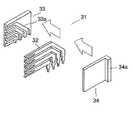
The second conventional technique will be described with reference to FIG.
[0005]
The
[0006]
Each
[0007]
After each
[0008]
[Patent Document 1]
Japanese Patent No. 2537698 (page 3,
[0009]
[Patent Document 2]
JP 2000-113928 A (page 3, column 4, line 38-page 4,
[0010]
[Problems to be solved by the invention]
In the first conventional technique, an expensive mold is required to insert-mold the lead frame into the insulator, and the manufacturing process of the contact module is complicated.
[0011]
In the second conventional technique, a separate part (the other resin mold member 34) is required, and an expensive mold for manufacturing the same is also required, and the assembly process of the contact module is complicated.
[0012]
Therefore, the present invention improves the drawbacks of the above two conventional techniques, eliminates the need for insert molding dies, separate parts and manufacturing dies, reduces the number of assembly parts, and is inexpensive. Is to provide.
[0013]
[Means for Solving the Problems]
The present invention employs the following means in order to solve the above problems.
[0014]
1. In the contact module composed of a plurality of contacts and an insulator for holding each contact, each contact includes a contact portion, a terminal portion, an intermediate portion connecting between the contact portion and the terminal portion, and The insulator has a plurality of grooves, a plurality of positioning portions, and a plurality of caulking portions, each of which accommodates the contacts, and the positioning portions and the positioning portions are engaged with each other. A contact module in which the contacts are positioned on the insulator by being combined, and the contacts are fixed to the insulator by deforming the caulking portions.
[0015]
2. The contact module according to claim 1, wherein the contacts are temporarily held by the insulator by press-fitting each of the positioned portions into the positioning portions.
[0016]
DETAILED DESCRIPTION OF THE INVENTION
A contact module according to an embodiment of the present invention will be described with reference to FIGS.
[0017]
FIG. 1 is a perspective view before the plug connector 3 attached to the backplane 1 by press-fitting and the receptacle connector 4 attached to the
[0018]
The plug connector 3 includes a
[0019]
The
[0020]
Each
[0021]
The
[0022]
In FIG. 5, each
[0023]
First, as shown in FIG. 4, the
[0024]
Next, as shown in FIGS. 5E to 5H, when the 17 crimping
[0025]
At this time, if the
[0026]
FIG. 6 is a cross-sectional view showing a process from when each
[0027]
FIG. 7 shows three methods of caulking. FIGS. 7A and 7B show states before and after the caulking of the first method in which the
[0028]
According to the present invention, as shown in FIG. 8, the
[0029]
【The invention's effect】
As will be apparent from the above description, the present invention provides the following effects.
[0030]
1. In the prior art, the required insert molding die or a separate part and its manufacturing die are not required in the present invention, so a contact module with a small number of assembly parts and a low cost is provided. Can be provided.
[0031]
2. Each contact is temporarily held by the insulator by press-fitting each positioned part and each positioning part, and each crimping part is deformed to fix the contact. Simple.
[Brief description of the drawings]
FIG. 1 is a perspective view of a plug connector employing a contact module according to an embodiment of the present invention and a receptacle connector before fitting.
FIG. 2 shows each socket contact in the contact module, wherein (A) shows a side view and (B) shows a front view.
3A and 3B are views of an insulator in the contact module, wherein FIG. 3A is a plan view, FIG. 3B is a front view, FIG. 3C is a side view, and FIG.
4A is a plan view of the contact module, FIG. 4B is a front view, FIG. 4C is a side view, and FIG. 4D is a bottom view.
FIGS. 5A and 5B are views of the contact module before and after fixing the socket contact to the insulator by caulking, where FIG. 5A is a plan view, FIG. 5B is a front view, FIG. 5C is a side view, and FIG. (E) is a front view of the crimped portion before crimping, (F) is a sectional view taken along line BB in FIG. (E), (G) is a front view of the crimped portion after crimping, (H) is (G) A sectional view taken along line CC in the figure is shown.
6 is a cross-sectional view of a process from when each socket contact in the contact module is inserted into each groove of the insulator to when it is fixed, and FIG. 6A is a diagram in which each socket contact is inserted into each groove of the insulator. In the previous state, (B) is a state in which each socket contact is inserted into each groove of the insulator, (C) is a sectional view taken along line AA in FIG. 5 (B), and each socket contact is caulked to the insulator. Each fixed state is shown.
7A and 7B are cross-sectional views of three methods for fixing the socket contact in the contact module to the insulator by caulking, in which FIG. 7A is a state before caulking of the first method, and FIG. 7B is caulking of the first method. (C) is the state before caulking of the second method, (D) is the state after caulking of the second method, (E) is the state before caulking of the third method, and (F) is The state after caulking of the third method is shown respectively.
8A is a plan view of the contact module, FIG. 8B is a plan view, FIG. 8B is a front view, FIG. 8C is a side view, FIG. 8D is a bottom view, and FIG. Front view of the crimped part before crimping, (F) is a sectional view taken along line BB in FIG. (E), (G) is a front view of the crimped part after crimping, and (H) is a line C in FIG. Cross-sectional views along -C are shown respectively.
FIG. 9 is a perspective view before assembly of a contact module according to a second prior art.
[Explanation of symbols]
1
DESCRIPTION OF
Claims (2)
Translated fromJapanese前記各コンタクトは、接触部、端子部、前記接触部と前記端子部との間を連結する中間部、及び、被位置決め部を有し、
前記インシュレータは、前記各コンタクトをそれぞれ収納する複数の溝、複数の位置決め部、及び、複数のカシメ部を有し、
前記各被位置決め部と前記各位置決め部とが係合することによって、前記各コンタクトが前記インシュレータに位置決めされ、かつ、前記各カシメ部を変形することによって、前記各コンタクトが前記インシュレータに固定されることを特徴とするコンタクトモジュール。In a contact module comprising a plurality of contacts and an insulator for holding each contact,
Each contact has a contact portion, a terminal portion, an intermediate portion connecting the contact portion and the terminal portion, and a positioned portion,
The insulator has a plurality of grooves for storing the contacts, a plurality of positioning portions, and a plurality of caulking portions,
When each of the positioned parts and each of the positioning parts are engaged, each of the contacts is positioned on the insulator, and by deforming each of the caulking parts, each of the contacts is fixed to the insulator. A contact module characterized by that.
Priority Applications (2)
| Application Number | Priority Date | Filing Date | Title |
|---|---|---|---|
| JP2002300467AJP3661149B2 (en) | 2002-10-15 | 2002-10-15 | Contact module |
| US10/834,061US7097506B2 (en) | 2002-10-15 | 2004-04-29 | Contact module in which mounting of contacts is simplified |
Applications Claiming Priority (1)
| Application Number | Priority Date | Filing Date | Title |
|---|---|---|---|
| JP2002300467AJP3661149B2 (en) | 2002-10-15 | 2002-10-15 | Contact module |
Publications (2)
| Publication Number | Publication Date |
|---|---|
| JP2004139745A JP2004139745A (en) | 2004-05-13 |
| JP3661149B2true JP3661149B2 (en) | 2005-06-15 |
Family
ID=32449153
Family Applications (1)
| Application Number | Title | Priority Date | Filing Date |
|---|---|---|---|
| JP2002300467AExpired - Fee RelatedJP3661149B2 (en) | 2002-10-15 | 2002-10-15 | Contact module |
Country Status (2)
| Country | Link |
|---|---|
| US (1) | US7097506B2 (en) |
| JP (1) | JP3661149B2 (en) |
Families Citing this family (54)
| Publication number | Priority date | Publication date | Assignee | Title |
|---|---|---|---|---|
| US6869292B2 (en) | 2001-07-31 | 2005-03-22 | Fci Americas Technology, Inc. | Modular mezzanine connector |
| CN100483886C (en)* | 2001-11-14 | 2009-04-29 | Fci公司 | Crosstalk reduction for electrical connectors |
| US6981883B2 (en)* | 2001-11-14 | 2006-01-03 | Fci Americas Technology, Inc. | Impedance control in electrical connectors |
| US20050196987A1 (en)* | 2001-11-14 | 2005-09-08 | Shuey Joseph B. | High density, low noise, high speed mezzanine connector |
| US7390200B2 (en) | 2001-11-14 | 2008-06-24 | Fci Americas Technology, Inc. | High speed differential transmission structures without grounds |
| US6994569B2 (en)* | 2001-11-14 | 2006-02-07 | Fci America Technology, Inc. | Electrical connectors having contacts that may be selectively designated as either signal or ground contacts |
| WO2005031922A2 (en) | 2003-09-26 | 2005-04-07 | Fci Americas Technology, Inc. | Improved impedance mating interface for electrical connectors |
| US7524209B2 (en)* | 2003-09-26 | 2009-04-28 | Fci Americas Technology, Inc. | Impedance mating interface for electrical connectors |
| US6971916B2 (en) | 2004-03-29 | 2005-12-06 | Japan Aviation Electronics Industry Limited | Electrical connector for use in transmitting a signal |
| US7281950B2 (en) | 2004-09-29 | 2007-10-16 | Fci Americas Technology, Inc. | High speed connectors that minimize signal skew and crosstalk |
| DE102004060782B3 (en)* | 2004-12-17 | 2006-03-09 | Harting Electronics Gmbh & Co. Kg | Screened, high-pole printed circuit board connector for transferring signals from one printed circuit board to another, has metallic housing in which disk-shaped segments are arranged and electrical contacts arranged within segments |
| US20060245137A1 (en)* | 2005-04-29 | 2006-11-02 | Fci Americas Technology, Inc. | Backplane connectors |
| US7083477B1 (en)* | 2005-07-29 | 2006-08-01 | International Business Machines Corporation | Providing mechanical support for modular interconnect systems |
| JP4190015B2 (en)* | 2005-11-02 | 2008-12-03 | 日本航空電子工業株式会社 | connector |
| DE202005020474U1 (en)* | 2005-12-31 | 2006-02-23 | Erni Elektroapparate Gmbh | Connectors |
| US7462924B2 (en)* | 2006-06-27 | 2008-12-09 | Fci Americas Technology, Inc. | Electrical connector with elongated ground contacts |
| US7500871B2 (en) | 2006-08-21 | 2009-03-10 | Fci Americas Technology, Inc. | Electrical connector system with jogged contact tails |
| US7713088B2 (en) | 2006-10-05 | 2010-05-11 | Fci | Broadside-coupled signal pair configurations for electrical connectors |
| US7708569B2 (en) | 2006-10-30 | 2010-05-04 | Fci Americas Technology, Inc. | Broadside-coupled signal pair configurations for electrical connectors |
| US7497736B2 (en) | 2006-12-19 | 2009-03-03 | Fci Americas Technology, Inc. | Shieldless, high-speed, low-cross-talk electrical connector |
| US7811100B2 (en) | 2007-07-13 | 2010-10-12 | Fci Americas Technology, Inc. | Electrical connector system having a continuous ground at the mating interface thereof |
| US8764464B2 (en) | 2008-02-29 | 2014-07-01 | Fci Americas Technology Llc | Cross talk reduction for high speed electrical connectors |
| JP5405582B2 (en) | 2008-11-14 | 2014-02-05 | モレックス インコーポレイテド | Resonance change connector |
| MY155071A (en) | 2008-12-12 | 2015-08-28 | Molex Inc | Resonance modifying connector |
| US9277649B2 (en) | 2009-02-26 | 2016-03-01 | Fci Americas Technology Llc | Cross talk reduction for high-speed electrical connectors |
| US8366485B2 (en) | 2009-03-19 | 2013-02-05 | Fci Americas Technology Llc | Electrical connector having ribbed ground plate |
| US8608510B2 (en) | 2009-07-24 | 2013-12-17 | Fci Americas Technology Llc | Dual impedance electrical connector |
| US7905751B1 (en)* | 2009-09-23 | 2011-03-15 | Tyco Electronics Corporation | Electrical connector module with contacts of a differential pair held in separate chicklets |
| US8267721B2 (en) | 2009-10-28 | 2012-09-18 | Fci Americas Technology Llc | Electrical connector having ground plates and ground coupling bar |
| US8616919B2 (en) | 2009-11-13 | 2013-12-31 | Fci Americas Technology Llc | Attachment system for electrical connector |
| CN102725919B (en) | 2009-12-30 | 2015-07-08 | Fci公司 | Electrical connector with impedance tuning ribs |
| US9136634B2 (en) | 2010-09-03 | 2015-09-15 | Fci Americas Technology Llc | Low-cross-talk electrical connector |
| US9312618B2 (en)* | 2011-08-08 | 2016-04-12 | Molex, Llc | Connector with tuned channel |
| EP2624034A1 (en) | 2012-01-31 | 2013-08-07 | Fci | Dismountable optical coupling device |
| US9257778B2 (en) | 2012-04-13 | 2016-02-09 | Fci Americas Technology | High speed electrical connector |
| US8944831B2 (en) | 2012-04-13 | 2015-02-03 | Fci Americas Technology Llc | Electrical connector having ribbed ground plate with engagement members |
| USD718253S1 (en) | 2012-04-13 | 2014-11-25 | Fci Americas Technology Llc | Electrical cable connector |
| USD727268S1 (en) | 2012-04-13 | 2015-04-21 | Fci Americas Technology Llc | Vertical electrical connector |
| USD727852S1 (en) | 2012-04-13 | 2015-04-28 | Fci Americas Technology Llc | Ground shield for a right angle electrical connector |
| USD751507S1 (en) | 2012-07-11 | 2016-03-15 | Fci Americas Technology Llc | Electrical connector |
| US9543703B2 (en) | 2012-07-11 | 2017-01-10 | Fci Americas Technology Llc | Electrical connector with reduced stack height |
| USD745852S1 (en) | 2013-01-25 | 2015-12-22 | Fci Americas Technology Llc | Electrical connector |
| USD720698S1 (en) | 2013-03-15 | 2015-01-06 | Fci Americas Technology Llc | Electrical cable connector |
| US9054432B2 (en)* | 2013-10-02 | 2015-06-09 | All Best Precision Technology Co., Ltd. | Terminal plate set and electric connector including the same |
| JP5943017B2 (en)* | 2014-02-21 | 2016-06-29 | 第一精工株式会社 | Electrical connector and electrical connector manufacturing method |
| JP5949804B2 (en)* | 2014-02-21 | 2016-07-13 | 第一精工株式会社 | Electrical connector and electrical connector manufacturing method |
| TWI600236B (en) | 2014-05-07 | 2017-09-21 | 鴻騰精密科技股份有限公司 | Electrical connector and method for making the same |
| US9722383B2 (en) | 2014-05-07 | 2017-08-01 | Foxconn Interconnect Technology Limited | Electrical connector having insulative housing and method of making the same |
| TWI573335B (en) | 2014-08-13 | 2017-03-01 | 鴻騰精密科技股份有限公司 | Electrical connector and method of making the same |
| TWI578633B (en) | 2014-08-22 | 2017-04-11 | 鴻騰精密科技股份有限公司 | Electrical connector and method of making the same |
| CN113131236B (en)* | 2019-12-31 | 2023-05-16 | 富鼎精密工业(郑州)有限公司 | Electric connector |
| CN113131265B (en)* | 2019-12-31 | 2023-05-19 | 富鼎精密工业(郑州)有限公司 | Electric connector |
| CN111430957B (en)* | 2020-03-03 | 2021-08-24 | 上海航天科工电器研究院有限公司 | Orthogonal direct contact type high-speed electric connector |
| EP4283793A4 (en)* | 2021-03-12 | 2024-07-17 | Huawei Technologies Co., Ltd. | CONNECTOR, FRAME DEVICE AND CONNECTOR ASSEMBLY METHOD |
Family Cites Families (6)
| Publication number | Priority date | Publication date | Assignee | Title |
|---|---|---|---|---|
| US4676576A (en)* | 1986-02-19 | 1987-06-30 | Burndy Corporation | Communications connector |
| ES2070283T3 (en) | 1989-10-10 | 1995-06-01 | Whitaker Corp | CONTRAPLANE CONNECTOR WITH ADAPTED IMPEDANCES. |
| JP3326522B2 (en) | 1998-10-05 | 2002-09-24 | 日本航空電子工業株式会社 | connector |
| US6409543B1 (en)* | 2001-01-25 | 2002-06-25 | Teradyne, Inc. | Connector molding method and shielded waferized connector made therefrom |
| US6551140B2 (en)* | 2001-05-09 | 2003-04-22 | Hon Hai Precision Ind. Co., Ltd. | Electrical connector having differential pair terminals with equal length |
| US6843487B1 (en)* | 2002-10-07 | 2005-01-18 | David Barry Lotman | Mobile lift assembly for a vehicle |
- 2002
- 2002-10-15JPJP2002300467Apatent/JP3661149B2/ennot_activeExpired - Fee Related
- 2004
- 2004-04-29USUS10/834,061patent/US7097506B2/ennot_activeExpired - Fee Related
Also Published As
| Publication number | Publication date |
|---|---|
| US7097506B2 (en) | 2006-08-29 |
| JP2004139745A (en) | 2004-05-13 |
| US20040201084A1 (en) | 2004-10-14 |
Similar Documents
| Publication | Publication Date | Title |
|---|---|---|
| JP3661149B2 (en) | Contact module | |
| JP2001006771A (en) | Connector | |
| US9825382B2 (en) | Low profile connector and assembly of the same | |
| JP2004127572A (en) | connector | |
| JP3356394B2 (en) | Electrical contacts | |
| US6067710A (en) | Method for manufacturing a memory card electrical connector with contacts having a ground terminal | |
| JP3122580B2 (en) | Relay connector | |
| US10096922B2 (en) | Rearview mirror assembly with biased electrical connection | |
| CN100502154C (en) | Electrical connector with wire management system | |
| US20040266229A1 (en) | Electrical connector having a spacer | |
| JP4727464B2 (en) | Joint connector | |
| JP2003173827A (en) | Cable holding structure of connector | |
| JPH05266871A (en) | Attachment structure for connection terminal of battery electrode of mobile device | |
| JP2002033145A (en) | ELECTRICAL CONNECTOR HAVING FIXING METAL AND METHOD OF MANUFACTURING THE SAME | |
| JP2002050436A (en) | Connector and manufacturing method thereof | |
| JP3540169B2 (en) | ID terminal | |
| JPH0350635Y2 (en) | ||
| JP2000215951A (en) | Board-mounting type connector | |
| JP2004152640A (en) | Connector and assembly method thereof | |
| JP2000021485A (en) | Contact and connector device provided with the contact | |
| JP2007242558A (en) | Terminal structure | |
| JPH06188035A (en) | Connector for printed circuit board | |
| WO1998028821A1 (en) | Memory card connector and contact retention system therefor and method of assembly thereof | |
| JP2913364B2 (en) | Surface mount connector and method for adjusting height of connection part | |
| JP2007502521A (en) | Spring-loaded electrical terminal |
Legal Events
| Date | Code | Title | Description |
|---|---|---|---|
| A977 | Report on retrieval | Free format text:JAPANESE INTERMEDIATE CODE: A971007 Effective date:20050210 | |
| TRDD | Decision of grant or rejection written | ||
| A01 | Written decision to grant a patent or to grant a registration (utility model) | Free format text:JAPANESE INTERMEDIATE CODE: A01 Effective date:20050223 | |
| A61 | First payment of annual fees (during grant procedure) | Free format text:JAPANESE INTERMEDIATE CODE: A61 Effective date:20050310 | |
| R150 | Certificate of patent or registration of utility model | Free format text:JAPANESE INTERMEDIATE CODE: R150 | |
| FPAY | Renewal fee payment (event date is renewal date of database) | Free format text:PAYMENT UNTIL: 20090401 Year of fee payment:4 | |
| FPAY | Renewal fee payment (event date is renewal date of database) | Free format text:PAYMENT UNTIL: 20090401 Year of fee payment:4 | |
| FPAY | Renewal fee payment (event date is renewal date of database) | Free format text:PAYMENT UNTIL: 20100401 Year of fee payment:5 | |
| FPAY | Renewal fee payment (event date is renewal date of database) | Free format text:PAYMENT UNTIL: 20100401 Year of fee payment:5 | |
| FPAY | Renewal fee payment (event date is renewal date of database) | Free format text:PAYMENT UNTIL: 20100401 Year of fee payment:5 | |
| LAPS | Cancellation because of no payment of annual fees |