JP3660638B2 - Clock extraction circuit - Google Patents
Clock extraction circuitDownload PDFInfo
- Publication number
- JP3660638B2 JP3660638B2JP2002089773AJP2002089773AJP3660638B2JP 3660638 B2JP3660638 B2JP 3660638B2JP 2002089773 AJP2002089773 AJP 2002089773AJP 2002089773 AJP2002089773 AJP 2002089773AJP 3660638 B2JP3660638 B2JP 3660638B2
- Authority
- JP
- Japan
- Prior art keywords
- phase
- output
- signal
- clock
- frequency
- Prior art date
- Legal status (The legal status is an assumption and is not a legal conclusion. Google has not performed a legal analysis and makes no representation as to the accuracy of the status listed.)
- Expired - Fee Related
Links
Images


Classifications
- H—ELECTRICITY
- H04—ELECTRIC COMMUNICATION TECHNIQUE
- H04L—TRANSMISSION OF DIGITAL INFORMATION, e.g. TELEGRAPHIC COMMUNICATION
- H04L7/00—Arrangements for synchronising receiver with transmitter
- H04L7/02—Speed or phase control by the received code signals, the signals containing no special synchronisation information
- H04L7/033—Speed or phase control by the received code signals, the signals containing no special synchronisation information using the transitions of the received signal to control the phase of the synchronising-signal-generating means, e.g. using a phase-locked loop
- H—ELECTRICITY
- H03—ELECTRONIC CIRCUITRY
- H03L—AUTOMATIC CONTROL, STARTING, SYNCHRONISATION OR STABILISATION OF GENERATORS OF ELECTRONIC OSCILLATIONS OR PULSES
- H03L7/00—Automatic control of frequency or phase; Synchronisation
- H03L7/06—Automatic control of frequency or phase; Synchronisation using a reference signal applied to a frequency- or phase-locked loop
- H03L7/08—Details of the phase-locked loop
- H03L7/081—Details of the phase-locked loop provided with an additional controlled phase shifter
- H03L7/0812—Details of the phase-locked loop provided with an additional controlled phase shifter and where no voltage or current controlled oscillator is used
- H03L7/0814—Details of the phase-locked loop provided with an additional controlled phase shifter and where no voltage or current controlled oscillator is used the phase shifting device being digitally controlled
- H—ELECTRICITY
- H03—ELECTRONIC CIRCUITRY
- H03L—AUTOMATIC CONTROL, STARTING, SYNCHRONISATION OR STABILISATION OF GENERATORS OF ELECTRONIC OSCILLATIONS OR PULSES
- H03L7/00—Automatic control of frequency or phase; Synchronisation
- H03L7/06—Automatic control of frequency or phase; Synchronisation using a reference signal applied to a frequency- or phase-locked loop
- H03L7/08—Details of the phase-locked loop
- H03L7/085—Details of the phase-locked loop concerning mainly the frequency- or phase-detection arrangement including the filtering or amplification of its output signal
- H03L7/089—Details of the phase-locked loop concerning mainly the frequency- or phase-detection arrangement including the filtering or amplification of its output signal the phase or frequency detector generating up-down pulses
- H—ELECTRICITY
- H04—ELECTRIC COMMUNICATION TECHNIQUE
- H04L—TRANSMISSION OF DIGITAL INFORMATION, e.g. TELEGRAPHIC COMMUNICATION
- H04L7/00—Arrangements for synchronising receiver with transmitter
- H04L7/02—Speed or phase control by the received code signals, the signals containing no special synchronisation information
- H04L7/033—Speed or phase control by the received code signals, the signals containing no special synchronisation information using the transitions of the received signal to control the phase of the synchronising-signal-generating means, e.g. using a phase-locked loop
- H04L7/0337—Selecting between two or more discretely delayed clocks or selecting between two or more discretely delayed received code signals
Landscapes
- Engineering & Computer Science (AREA)
- Computer Networks & Wireless Communication (AREA)
- Signal Processing (AREA)
- Stabilization Of Oscillater, Synchronisation, Frequency Synthesizers (AREA)
- Synchronisation In Digital Transmission Systems (AREA)
- Optical Communication System (AREA)
Description
Translated fromJapanese【0001】
【発明の属する技術分野】
本発明は、クロック抽出回路に関するもので、例えば高速データ通信に使用されるものである。
【0002】
【従来の技術】
データ通信システムにおいて、互いに異なるクロック信号源を有する通信機器間でシリアル伝送を行うには、受信側の通信機器で送信側の通信機器と同一周波数のクロックを必要とする。この際、受信側では、周波数オフセットが発生してしまうので、受信データと同期したサンプリングクロックを生成させ、このクロックで受信データをサンプリングして再生データを得ている。
【0003】
受信データと同期したサンプリングクロックを生成させるクロック抽出回路には種々の方式のものがあるが、その1つに多相クロックを使用したクロック抽出回路がある。この方式では、n相の多相クロックを使用し、位相比較器で受信データの立ち上がり(または立ち下がり)エッジとn相クロックから選択した抽出クロックのエッジまでの位相を比較し、最適クロックに至るまでn相クロックから最適クロックを選択している。
【0004】
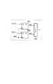
図8は、従来の多相クロックを使用したクロック抽出回路の一例を示す。
【0005】
図8中、310 はバイナリ型の位相比較器、320 は周波数削減器、330 は制御信号生成器、340 は位相制御回路、350 は分周器である。
【0006】
バイナリ型の位相比較器310 は、位相制御回路340 により生成された位相が90°ずつずれた4相の抽出クロックiclk,qclk,iclkb,qclkb を用いて受信データを読み取り、受信データに対する抽出クロックの位相の遅れ・進みを2値で判定し、判定結果をUP信号、DN信号により出力する。
【0007】
この場合、抽出クロックiclk,qclk,iclkb,qclkb を用いて読み取った受信データの値を比較すれば、抽出クロックiclk,qclk,iclkb,qclkb のうちのどれとどれのクロックの間で読み取った値が変わったかが判るので、抽出クロックの位相が受信データに対して進んでいるか遅れているかを判定できる。
【0008】
上記位相比較器310 は、抽出クロックの位相が受信データの位相より遅れている場合には出力信号UPを"High"、進んでいる場合には出力信号DNを"High"にする。ここで、出力信号UPの"High"は、位相制御回路340 から出力される4相の抽出クロックiclk,qclk,iclkb,qclkb の位相を進める意味を持ち、出力信号DNの"High"は、位相制御回路340 から出力される4相の抽出クロックの位相を遅らせるという意味を持つ。
【0009】
上記バイナリ型の位相比較器310 の伝達関数のゲインは非常に高いので、クロック抽出系でループゲインが高くなり、系が不安定になってしまう。そこで、クロック抽出系のループゲインを下げるために、位相比較器310 からの出力信号UP/DN の周波数を周波数削減器320 で落とす(間引く)。
【0010】
即ち、周波数削減器320 は、受信データが遷移した時に得られる位相比較結果(抽出クロックの位相が進んでいるか遅れているかの情報)を大きな割合で削減するものであり、その周波数削減比は分周器350 の分周比の数倍以上に設定されている。例えば、16個のUP(またはDN)出力が発生したら、1個の低い周波数の信号UP_LF(またはDN_LF)を生成する。
【0011】
制御信号生成器330 は、周波数削減器320 から出力する信号UP_LF 、DN_LF を受け、例えば64ビットの制御信号PCNT[63:0]を生成するものである。
【0012】
図9は、図8中の制御信号生成器330 の一例を示している。
【0013】
この制御信号生成器330 は、データ入力D として周波数削減器320 の出力信号UP_LF 、DN_LF が対応して入力し、クロック入力として分周器350 の分周出力RBC が入力する2つのフリップフロップ回路331,332 と、この2つのフリップフロップ回路331,332 の各出力INC 、DEC によりデータシフト方向が制御される例えば64ビットのシフタ333 を有する。
【0014】
この制御信号生成器330 は、入力信号UP_LF 、DN_LF に基づいてシフタ333 内の"1"の位置をシフトし、この1"の位置を表わす64ビットの制御信号PCNT[63:0]を生成する。
【0015】
図8中の位相制御回路340 は、位相が90°ずつ異なる4相のクロック信号CLK0、CLK90 、CLK180、CLK270が入力するスイッチ回路群を有し、このスイッチ回路群のうちのどのスイッチ回路をopen/closeするかが御信号生成器330 から出力する制御信号PCNT[63:0]によって制御される。これにより、4相のクロック信号CLK0、CLK90 、CLK180、CLK270から所望の位相のクロック信号を生成する(4相の抽出クロック信号iclk,qclk,iclkb,qclkb の位相を調整する)。
【0016】
この場合、抽出クロック信号iclk,qclk,iclkb,qclkb の一回の位相修正量は常に一定である。一回の位相修正量が大きいと、抽出クロック信号iclk,qclk,iclkb,qclkb のジッタが大きくなるので、系を安定化させるためには一回の位相修正量をあまり大きくすることができない。
【0017】
図8中の分周器350 は、位相制御回路340 で位相が調整された抽出クロックを分周して分周出力RBC を生成し、周波数削減器320 と制御信号生成器330 に供給するものである。
【0018】
上記したように従来のクロック抽出回路は、周波数削減器320 で間引いた信号を用いて制御信号PCNT[63:0]を生成し、制御信号PCNT[63:0]により位相制御回路340 を制御して生成された抽出クロックiclk,qclk,iclkb,qclkb を用いて受信データをサンプリングして受信データを認識し、再生データを得ている。
【0019】
ところで、例えばUSB(Universal Serial Bus)2.0規格のHi-speedモード時は受信データの変化しない最長ビット長が7ビット、8B10B 伝送方式では受信データの変化しない最長ビット長が9ビットと規定されている。このような規格、方式を採用した実際のデータ通信において、従来のクロック抽出回路は、以下に述べるような問題があった。
【0020】
即ち、受信データの値が遷移しなければ位相比較器310 の出力信号UP,DN が生成されず、受信データの値が遷移しない期間が長い場合は、受信データと抽出クロック信号iclk,qclk,iclkb,qclkb の位相差を詰める制御が働かない。このような状態の時に受信データの値が遷移して位相比較器310 が出力信号UP,DN を出したとしても、抽出クロック信号iclk,qclk,iclkb,qclkb は理想的な位置(位相)から外れている。この抽出クロック信号iclk,qclk,iclkb,qclkb の位相を理想的な位置に修正しようとしても、位相比較結果を大きく間引いてしまっているので、直ぐには抽出クロック信号iclk,qclk,iclkb,qclkb の位相を理想的な位置に修正できず、多くの受信データの読み取りエラーを起こしてしまう。
【0021】
このような問題の根源は、周波数削減器320 で位相比較器310 の出力の周波数を必要以上に下げた(間引いた)ことにある。
【0022】
【発明が解決しようとする課題】
上記したように従来のクロック抽出回路は、受信データの値の遷移のない期間が長い場合に抽出クロックの位相を理想的な位置に修正しようとしても、抽出クロックの位相を理想的な位置に直ぐには修正できず、多くの受信データの読み取りエラーを起こしてしまうという問題があった。
【0023】
本発明は上記の問題点を解決すべくなされたもので、受信データの値の遷移のない期間が長い場合でも読み取り誤りがなく、かつ、平衡状態でのクロック抽出系は安定に動作し、大きな修正が必要な場合は高い追従性を併せ持つ理想的なクロック抽出系を実現し得るクロック抽出回路を提供することを目的とする。
【0024】
【課題を解決するための手段】
本発明のクロック抽出回路は、入力データと複数の各抽出クロックとの位相差を検出する位相比較器と、前記位相比較器の出力の周波数を、周波数削減制御入力により指定される所定の割合で下げる周波数削減器と、前記周波数削減器の出力信号の頻度を監視し、位相を進める信号もしくは遅らせる信号が均等に出力されている場合は抽出クロックの位相を小さく調節し、位相を進める信号もしくは遅らせる信号のうちどちらか一方の信号が多く出力される場合は抽出クロックの位相を大きく調節するための位相制御信号を生成する制御信号生成器と、位相が異なる複数相のクロック信号が入力するスイッチ回路群を有し、前記制御信号生成器から出力する位相制御信号に応じて上記スイッチ回路群を制御して、上記複数相のクロック信号のうち2つのクロック信号を所望の重み精度で合成することで位相が調整された前記複数の抽出クロックを出力する位相制御回路と、前記位相制御回路から出力する抽出クロックを分周し、分周出力により前記周波数削減器の周波数削減の割合を指定するように制御する分周器とを具備することを特徴とする。
【0025】
【発明の実施の形態】
以下、図面を参照して本発明の実施の形態を詳細に説明する。
【0026】
<第1の実施形態>
図1は、本発明の第1の実施形態に係るクロック抽出回路を示している。
【0027】
このクロック抽出回路は、例えば1個の半導体集積回路に形成されており、図8を参照して前述した従来のクロック抽出回路と比べて、周波数削減器120 および制御信号生成器130 が異なり、その他は同じである。
【0028】
図2は、図1中の位相比較器110 の動作例を示すタイミング波形図である。
【0029】
図1中、110 はバイナリ型の位相比較器、120 は周波数削減器、130 は制御信号生成器、140 は位相制御回路、150 は分周器である。
【0030】
バイナリ型の位相比較器110 は、図8を参照して前述した位相比較器310 と同様に、後述する位相制御回路140 により生成された位相が90°ずつずれた4相の抽出クロックiclk,qclk,iclkb,qclkb を用いて入力データ(本例では受信データ)を読み取り、受信データに対する抽出クロックiclk,qclk,iclkb,qclkb の位相の遅れ・進みを2値で判定し、判定結果をUP信号、DN信号として出力する。
【0031】
この場合、抽出クロックiclk,qclk,iclkb,qclkb で読み取った受信データの値を比較すれば、抽出クロックiclk,qclk,iclkb,qclkb のうちのどれとどれのクロックの間で読み取った値が変わったかが判るので、抽出クロックの位相が受信データに対して進んでいるか遅れているかを判定できる。
【0032】
上記位相比較器110 は、抽出クロックの位相が受信データの位相より遅れている場合には出力信号UPを"High"、進んでいる場合には出力信号DNを"High"にする。ここで、出力信号UPの"High"は、位相制御回路340 から出力される4相の抽出クロックiclk,qclk,iclkb,qclkb の位相を進める意味を持ち、出力信号DNの"High"は、位相制御回路340 から出力される4相の抽出クロックの位相を遅らせるという意味を持つ。
【0033】
上記位相比較器110 の出力信号UP,DN の周波数が高過ぎると、後段の回路の動作が困難であるので、位相比較器110 の出力信号UP,DN を周波数削減器120 で受けて、UP,DN の周波数を下げた信号UP_LF,DN_LF を出力する。
【0034】
制御信号生成器130 は、周波数削減器120 の出力信号UP_LF 、DN_LF を受け、UP_LF とDN_LF を累積し、その値を一定時間間隔で(定期的に)モニターし、累積値によって抽出クロックの位相修正量を段階的に制御するための例えば64ビットの制御信号PCNT[63:0]を生成するものである。
【0035】
位相制御回路140 は、位相が90°ずつ異なる4相のクロック信号CLK0、CLK90 、CLK180、CLK270が入力するスイッチ回路群を有し、このスイッチ回路群のうちのどのスイッチ回路をオン/オフするかを前記制御信号生成器130 からの制御信号PCNT[63:0]により制御することにより、抽出クロックの位相を調整し、出力クロック信号iclk,qclk,iclkb,qclkb の位相を調整する。
【0036】
分周器150 は、位相制御回路140 で位相が調整された抽出クロックを分周して分周出力RBC を生成し、前記周波数削減器120 と制御信号生成器130 に供給するものである。
【0037】
図3は、図1中の周波数削減器120 の構成の一例を示している。
【0038】
電源電位VDD が与えられるVDD ノードと接地電位VSS が与えられるVSS ノードとの間に、定電流源121 、スイッチ素子S1、スイッチ素子S2および定電流源122が直列に接続されている。スイッチ素子S1は位相比較器110 の出力信号UPによりスイッチ制御され、スイッチ素子S2は位相比較器110 の出力信号DNによりスイッチ制御される。
【0039】
上記スイッチ素子S1, S2の接続ノードとVSS ノードとの間に充放電用の容量123 が接続されている。また、前記VDD の半分の電位0.5*VDD が与えられる0.5*VDD ノードと上記スイッチ素子S1, S2の接続ノードとの間に初期値設定用のスイッチ素子S3が接続されている。
【0040】
そして、上記スイッチ素子S1, S2の接続ノードの電位は、第1の電圧比較回路(COMP1)124で第1の基準電位(上限電位)PSと比較されるとともに、第2の電圧比較回路(COMP2)125で第2の基準電位(下限電位)NGと比較される。これらの電圧比較回路124,125 の各出力は対応して2つのフリップフロップ回路(F/F)126,127のデータ入力D として入力する。
【0041】
上記2つのフリップフロップ回路126,127 は、分周器150 の分周出力クロックRBC が入力し、各出力信号UP_LF 、DN_LF を後段の制御信号生成器130 に供給する。この場合、上記各出力信号UP_LF 、DN_LF は、排他的オアゲート128 に入力し、この排他的オアゲート128 の出力により前記初期値設定用のスイッチ素子S3をスイッチ制御する。
【0042】
図3に示した周波数削減器は、充放電用の容量123 の充放電を利用して入力信号UP、DNより周波数が低い出力信号UP_LF 、DN_LF を生成するように動作する。
【0043】
即ち、入力信号UPが活性状態の期間は容量123 を充電し、入力信号DNが活性状態の期間は容量123 を放電する。このような充放電動作が行われる際、容量123の一端電位(スイッチ素子S1, S2の接続ノードの電位)が上限電位PSを超えたら、第1の電圧比較回路124 の出力が"High"になり、フリップフロップ回路126 の出力信号UP_LF が"High"になる。これに対して、容量123 の一端電位が下限電位NGより低くなったら、第2の電圧比較回路127 の出力信号が"High"になり、フリップフロップ回路127 の出力信号DN_LF が"High"になる。
【0044】
この場合、2つのフリップフロップ回路126,127 は、分周器150 の分周出力クロックRBC に同期して電圧比較回路124,125 の出力信号をデータ入力D として取り込み、後段の回路が動作し易くなるような出力信号UP_LF,DN_LF を生成している。
【0045】
この出力信号UP_LF もしくはDN_LF が出力された("High"になった)時、排他的オアゲート128 の出力が"High"になり、スイッチ素子S3がオンになり、容量123 の一端電位が初期値0.5*VDD に戻される。
【0046】
従って、周波数削減器120 は、信号UP、DNが"所望の回数"だけ入力した時に、出力信号UP_LF,DN_LF が分周クロックRBC の1周期の期間にわたって"High"になる。ここで言う"所望の回数"は、容量123 を充放電する定電流源121 、122 の電流と容量123 の容量値の比より決定される。
【0047】
本実施形態では、上記"所望の回数"を必要以上に大きくしないことを特徴とする。即ち、高速クロックiclkと低速クロックBRC の比(分周器150 の分周比)をN (正の整数)で表わした場合に、現実的には"所望の回数"の下限は"N 回"であるから、"所望の回数"をN もしくはN+数回に抑えるようにする。これは、容量123 を充放電する定電流源121 、122 の電流値を大きく設計しておく、あるいは、電流値が異なる複数の定電流源を形成しておき、ユーザーに応じて所望の定電流源を例えばレジスタの設定データにより選択制御するように構成することで、容易に実現可能である。
【0048】
上記したように"所望の回数"をN もしくはN+数回に抑えるようにしておくと、受信データの遷移が少ない場合、貴重な位相比較結果を可能な限り抽出クロックの位相修正に割り当てることができる。"所望の回数"を2N〜3Nとしてもよいが、4N以上にすると、従来と同様の問題が発生するおそれが高くなる。換言すれば、本実施形態では、周波数削減器120 による周波数削減の割合は、N 〜3Nの間になるように制御可能である。
【0049】
一方、位相比較結果をあまり高い頻度で抽出クロックの位相修正に反映させると、制御系のループゲインが高くなりすぎて、制御系が不安定になってしまう。そこで、周波数削減器120 の入力信号UP、DNの周波数を下げた出力信号UP_LF 、DN_LF の出力頻度を制御信号生成器130 でモニターし、その傾向によって、抽出クロックの位相修正量を変えるようにしている。
【0050】
図4は、図1中の制御信号生成器130 の構成の一例を示している。
【0051】
この制御信号生成器130 は、2つのフリップフロップ回路(F/F)131,132と、入力信号UP_LF とDN_LF の累積値を計算するための累積器133 と、この累積器133の累積値を定期的(一定時間毎)にモニター処理するためのカウンタ134 およびフリップフロップ回路(F/F)137と、アンドゲート135,136 と、シフト量算出器138 と、透過制御器139 と、デコーダ13A が設けられている。
【0052】
上記2つのフリップフロップ回路131,132 は、データ入力D として周波数削減器120 からの入力信号UP_LF 、DN_LF が入力し、クロック入力として分周器150の分周出力クロックRBC が入力し、データ出力Q として出力信号INC0,DEC0 を生成する。これらの信号INC0,DEC0 はアンドゲート135,136 に入力する。
【0053】
カウンタ134 は、分周器150 の分周出力クロックRBC をカウントし、カウント値がある値に達したらモニターパルス信号monitor を出力する。フリップフロップ回路137 は、クロック入力として上記信号monitor が入力し、累積器133 の累積値を格納する。
【0054】
また、カウンタ134 は相補的なリセット信号reset,resetbを出力する。この場合、上記したようなモニター処理を行っている期間はリセット信号reset が非活性状態、反転リセット信号resetbが活性状態になり、モニター処理が終了した後のタイミングでリセット信号reset が活性状態、反転リセット信号resetbが非活性状態になる。上記反転リセット信号resetbはアンドゲート135,136 を制御し、リセット信号reset は累積器133 および透過制御器139 を制御する。
【0055】
シフト量算出器138 は、前記フリップフロップ回路137 に格納された累積値に基づいて、抽出クロックの位相を大きく修正するための信号を生成する。この際、累積値がUP側に例えば4以上8未満の値であるなら、位相を一気に4段階進める信号INC4を"H" にし、累積値がUP側に8以上の値であるなら、位相を一気に8段間進める信号INC8を"H" にする。DN側についても上記UP側と同様に、累積値がDN側に4以上8未満の値であるなら、位相を一気に4段階遅らせる信号DEC4を"H"にし、累積値がDN側に8以上の値であるなら、位相を一気に8段間遅らせる信号DEC8を"H" にする。
【0056】
上記したように制御信号生成器130 が周波数削減器120 の出力信号UP_LF、DN_LF の頻度をモニターすることにより、抽出クロックの位相修正量を調整する準備が整う。
【0057】
抽出クロックの位相修正を実際に行う際には、アンドゲート135,136 の出力信号(位相比較結果を忠実に反映している信号)INC,DEC とシフト量算出器138 の出力信号(大きな位相修正量を持つ)INC4,INC8,DEC4,DEC8 の中から所望のものを選択する必要がある。この機能を実現するためにカウンタ134 、アンドゲート135,136 および透過制御器139 が用いられる。
【0058】
即ち、カウンタ134 から出力する反転リセット信号resetbが"H" (リセット信号reset が"L" )の期間には、フリップフロップ回路131,132 の出力信号INC0,DEC0 がアンドゲート135,136 を経て位相比較結果を忠実に反映している信号INC,DEC として出力する。この期間は、透過制御器139 の透過動作はオフになる。
【0059】
これに対して、カウンタ134 から出力するリセット信号reset が"H" (反転リセット信号resetbが"L" )の期間には、透過制御器139 の透過動作をオンにし、シフト量算出器138 の出力を透過させるとともに累積器133 の累積値をリセットする。この期間は、アンドゲート135,136 は閉じてINC,DEC は無効化される。
【0060】
このような動作により、カウンタ134 から定期的に出力するモニター信号monitor により累積器133 の累積値を読む時以外は、位相比較結果を忠実に反映するINC,DEC を選択して後段のデコーダ13A に伝える。これに対して、累積器133 の累積値の累積値を読む時は、UP_LF,DN_LF の頻度を考慮した位相修正量の大きなシフト量算出器138 からの出力INC4,INC8,DEC4,DEC8 を選択して後段のデコーダ13A に伝える。
【0061】
デコーダ13A は、前記信号INC,DEC,INC4,INC8,DEC4,DEC8 が入力し、位相制御回路140 における抽出クロックの位相修正量を段階的に決めるための例えば64ビットの制御信号PCNT[63:0]に変換するために設けられている。この制御信号PCNT[63:0]は、位相比較結果を忠実に反映する信号INC,DEC のいずれかが活性状態の場合には抽出クロックの位相修正量を小さく制御し、大きな修正量を持つ信号INC4,INC8,DEC4,DEC8 のいずれかが活性状態の場合には抽出クロックの位相修正量を大きくするものである。
【0062】
図5は、図4中のデコーダ13A の構成の一例を示している。
【0063】
図5において、シフト量生成器50は、前記信号INC,DEC,INC4,INC8,DEC4,DEC8により対応して6個のマルチプレクサ51を制御し、所要のシフト量データを選択して出力するものである。この場合、信号INC が活性状態の場合にはマルチプレクサ51は+1のシフト量データを選択し、信号INC4が活性状態の場合にはマルチプレクサ51は+4のシフト量データを選択し、信号INC8が活性状態の場合にはマルチプレクサ51は+8のシフト量データを選択し、信号DEC が活性状態の場合にはマルチプレクサ51は-1のシフト量データを選択し、信号DEC4が活性状態の場合にはマルチプレクサ51は-4のシフト量データを選択し、信号DEC8が活性状態の場合にはマルチプレクサ51は-8のシフト量データを選択する。
【0064】
シフタ52は、64ビットの循環型シフトレジスタのうちの連続する16ビットに"1" 、残りに"0" が書き込まれており、シフト量生成器50からのシフト量データによってデータシフト方向(インクレメントまたはデクレメント)およびデータシフト量が制御される。この場合、+1あるいは-1のシフト量データによって1 ビットのデータシフトが行われ、+4あるいは-4のシフト量データによって4 ビットのデータシフトが行われ、+8あるいは-8のシフト量データによって8 ビットのデータシフトが行われる。
【0065】
このような動作により、64ビットの循環型シフトレジスタの出力は、累積値によって抽出クロックの位相修正量を段階的に制御するための制御信号PCNT[63:0]として使用することが可能になる。ここで、64ビットの循環型シフトレジスタを4 グループに分割し、第1グループの連続する16ビットの出力を制御信号1[15:0] 、第2グループの連続する16ビットの出力を制御信号2[15:0] 、第3グループの連続する16ビットの出力を制御信号3[15:0] 、第4グループの連続する16ビットの出力を制御信号4[15:0] と命名する。
【0066】
図6は、図1中の位相制御回路140 の構成の一例を示している。
【0067】
図6に示す位相制御回路は、位相が90°づづ異なる4相のクロック信号CLK0,CLK90,CLK180,CLK270のうちの逆相の2つのクロック信号(CLK0,CLK180),(CLK90,CLK270), (CLK180,CLK0),(CLK270,CLK90)がそれぞれ対応して入力する第1の差動比較回路61〜第4の差動比較回路64を並列に接続している。この4個の差動比較回路61〜64は、負荷抵抗RLを共有しており、出力ノードには積分用コンデンサCを用いた積分器65と差動アンプ66が接続されている。
【0068】
そして、各差動比較回路61〜64の定電流源部を構成する16個のスイッチトランジスタTrのうちオンにする数を、各差動比較回路61〜64に対応して、図5中のシフタ53から入力する制御信号1[15:0] 、2[15:0] 、3[15:0] 、4[15:0] により切り換える(トランジスタのサイズを切り換える)。これにより、4相のクロック信号CLK0,CLK90,CLK180,CLK270のうちの2つのクロック信号を16ステップの重み精度で合成することによって所望の位相(16ステップの精度:90/16=5.625 °)のクロック信号を作り出すことが可能になる。
【0069】
図7は、図6の位相制御回路140 の動作の一例を示している。
【0070】
例えばクロック信号CLK0の位相を100 %使う場合は、第1の差動比較回路61の定電流源部のスイッチトランジスタを全てオンにし、他の差動比較回路62〜64の定電流源部のスイッチトランジスタを全てオフにするように、制御信号1[15:0]を全て"H" 、制御信号2[15:0] 、3[15:0] 、4[15:0] を全て"L" に設定する。
【0071】
また、クロック信号CLK0より90°遅れたクロック信号CLK90 の位相を100 %使う場合は、第2の差動比較回路62の定電流源部のスイッチトランジスタを全てオンにし、他の差動比較回路61、63、64の定電流源部のスイッチトランジスタを全てオフにするように、制御信号2[15:0] を全て"H" 、制御信号1[15:0] 、3[15:0] 、4[15:0] を全て"L" に設定する。
【0072】
さらに、位相が90°ずつ異なる4相の入力クロック信号CLK0,CLK90,CLK180,CLK270から隣接する2つを選び、それらの位相を所望の重みを付けて掛け合わせることにより、所望の中間の位相を持ったクロック信号を生成できる。
【0073】
例えば、CLK0とCLK90 を50% ずつの重みで重ね合わせれば、CLK0とCLK90 の中間の位相を持ったクロック信号が生成できる。この場合、制御信号1[15:8] を全て"H" 、制御信号1[7:0]を全て"L" 、制御信号2[15:8] を全て"L" 、制御信号2[7:0]を全て"H" 、制御信号3[15:0] 、4[15:0] を全て"L" に設定する。
【0074】
もし、掛け合わせにより生成されるクロック信号の位相を進めたければ、CLK0を60%、CLK90 を40%というように、位相が進んだ側のクロック信号CLK0の重みを上げて掛け合わせればよい。
【0075】
このような動作により、位相制御回路140 は、4つの入力クロック信号CLK0,CLK90,CLK180,CLK270から、受信データDATAのデータアイの中心に位相が合わせられたクロック信号iclkとその反転クロック信号iclkb 、並びに上記クロック信号iclkから90°位相が遅れたクロック信号qclkとその反転クロック信号qclkb を生成して出力する。
【0076】
上記したように本実施形態においては、位相比較器出力の周波数を落とす割合を必要最低限に止め、周波数の下がった位相比較結果を位相調整に反映させる。この時、周波数の下がった位相修正信号の出力頻度に応じて一回の位相修正量を調整するようにし、安定状態では位相修正量を小さくし、抽出クロックの位相が理想位置より大きくずれている時は位相修正量を大きくするように制御する。
【0077】
即ち、上記した本実施形態によれば、数少ない貴重な位相比較結果を抽出クロックの位相修正に高い頻度で反映させるので、データ遷移のない期間が長くても読み取り誤りがなく、かつ、平衡状態での系のループゲインは小さく(系が安定)、大きな修正が必要な場合は系のループゲインが大きいので、高い追従性を併せ持つ理想的なクロック抽出系を実現することができる。したがって、受信データの変化しない最長ビット長が規制してあるデータ伝送方式に適している。
【0078】
【発明の効果】
上述したように本発明クロック抽出回路によれば、受信データの値の遷移のない期間が長い場合でも読み取り誤りがなく、かつ、平衡状態でのクロック抽出系は安定に動作し、大きな修正が必要な場合は高い追従性を併せ持つ理想的なクロック抽出系を実現することができる。
【図面の簡単な説明】
【図1】本発明の第1の実施形態に係るクロック抽出回路を示すブロック図。
【図2】図1中の位相比較器の動作例を示すタイミング波形図。
【図3】図1中の周波数削減器の一例を示す回路図。
【図4】図1中の制御信号生成器の一例を示す回路図。
【図5】図4中のデコーダの一例を示す回路図。
【図6】図1中の位相制御回路の一例を示す回路図。
【図7】図6の位相制御回路の動作の一例を示すタイミング波形図。
【図8】従来の多相クロックを使用したクロック抽出回路の一例を示すブロック図。
【図9】図8中の制御信号生成器の一例を示す回路図。
【符号の説明】
110 …バイナリ型の位相比較器、
120 …周波数削減器、
130 …制御信号生成器、
140 …位相制御回路、
150 …分周器。[0001]
BACKGROUND OF THE INVENTION
The present invention relates to a clock extraction circuit, and is used, for example, for high-speed data communication.
[0002]
[Prior art]
In a data communication system, in order to perform serial transmission between communication devices having different clock signal sources, a communication device on the reception side needs a clock having the same frequency as that of the communication device on the transmission side. At this time, since a frequency offset occurs on the receiving side, a sampling clock synchronized with the received data is generated, and the received data is sampled with this clock to obtain reproduced data.
[0003]
There are various types of clock extraction circuits for generating a sampling clock synchronized with received data, and one of them is a clock extraction circuit using a multiphase clock. In this method, an n-phase multi-phase clock is used, and a phase comparator compares the rising (or falling) edge of received data with the phase from the n-phase clock to the edge of the selected extraction clock to reach the optimum clock. The optimum clock is selected from the n-phase clocks.
[0004]
FIG. 8 shows an example of a clock extraction circuit using a conventional multiphase clock.
[0005]
In FIG. 8, 310 is a binary type phase comparator, 320 is a frequency reducer, 330 is a control signal generator, 340 is a phase control circuit, and 350 is a frequency divider.
[0006]
The
[0007]
In this case, if the values of the received data read using the extracted clocks iclk, qclk, iclkb, qclkb are compared, the value read between any of the extracted clocks iclk, qclk, iclkb, qclkb and which clock Since it can be determined whether it has changed, it can be determined whether the phase of the extracted clock is advanced or delayed with respect to the received data.
[0008]
The
[0009]
Since the transfer function gain of the
[0010]
That is, the
[0011]
The
[0012]
FIG. 9 shows an example of the
[0013]
The
[0014]
The
[0015]
The
[0016]
In this case, the amount of one phase correction of the extracted clock signals iclk, qclk, iclkb, qclkb is always constant. If the amount of phase correction at one time is large, the jitter of the extracted clock signals iclk, qclk, iclkb, qclkb increases, so that the amount of phase correction at one time cannot be increased so much in order to stabilize the system.
[0017]
A
[0018]
As described above, the conventional clock extraction circuit generates the control signal PCNT [63: 0] using the signal thinned out by the
[0019]
By the way, for example, in the USB (Universal Serial Bus) 2.0 standard Hi-speed mode, the longest bit length that the received data does not change is 7 bits, and in the 8B10B transmission system, the longest bit length that the received data does not change is 9 bits. . In actual data communication employing such a standard and method, the conventional clock extraction circuit has the following problems.
[0020]
That is, if the value of the received data does not transition, the output signals UP and DN of the
[0021]
The root of such a problem is that the frequency reducer 320 lowers the frequency of the output of the
[0022]
[Problems to be solved by the invention]
As described above, the conventional clock extraction circuit immediately adjusts the phase of the extracted clock to the ideal position even if the phase of the extracted clock is corrected to the ideal position when the period without the transition of the received data value is long. Could not be corrected, causing a problem of reading many received data.
[0023]
The present invention has been made in order to solve the above-described problems. There is no reading error even when the period of time when there is no transition of the value of the received data is long, and the clock extraction system in the balanced state operates stably and is large. An object of the present invention is to provide a clock extraction circuit capable of realizing an ideal clock extraction system having high followability when correction is required.
[0024]
[Means for Solving the Problems]
The clock extraction circuit of the present invention includes input data andMultiple each A phase comparator that detects a phase difference from the extracted clock, a frequency reducer that reduces the frequency of the output of the phase comparator at a predetermined rate specified by a frequency reduction control input, and an output signal of the frequency reducer When the frequency is monitored and the signal that advances or delays the phase is output evenly, adjust the phase of the extracted clock to a smaller value, and either the signal that advances or delays the phase is output more Is a control signal generator that generates a phase control signal for greatly adjusting the phase of the extracted clock;It has a switch circuit group to which clock signals of different phases are input, Phase control signal output from the control signal generatorAnd controlling the switch circuit group in accordance with the above and synthesizing two clock signals of the plurality of clock signals with a desired weight accuracy. The phase adjustedplural A phase control circuit that outputs an extraction clock; and a frequency divider that divides the extraction clock output from the phase control circuit and controls the frequency reduction ratio of the frequency reducer to be specified by the frequency division output. It is characterized by doing.
[0025]
DETAILED DESCRIPTION OF THE INVENTION
Hereinafter, embodiments of the present invention will be described in detail with reference to the drawings.
[0026]
<First Embodiment>
FIG. 1 shows a clock extraction circuit according to the first embodiment of the present invention.
[0027]
This clock extraction circuit is formed, for example, in one semiconductor integrated circuit, and differs from the conventional clock extraction circuit described above with reference to FIG. 8 in that the
[0028]
FIG. 2 is a timing waveform diagram showing an operation example of the
[0029]
In FIG. 1, 110 is a binary type phase comparator, 120 is a frequency reducer, 130 is a control signal generator, 140 is a phase control circuit, and 150 is a frequency divider.
[0030]
Similarly to the
[0031]
In this case, if the received data values read by the extracted clocks iclk, qclk, iclkb, qclkb are compared, it can be determined which of the extracted clocks iclk, qclk, iclkb, qclkb and which clock the read value has changed. Therefore, it can be determined whether the phase of the extracted clock is advanced or delayed with respect to the received data.
[0032]
The
[0033]
If the frequency of the output signals UP and DN of the
[0034]
The
[0035]
The
[0036]
The
[0037]
FIG. 3 shows an example of the configuration of the
[0038]
A constant
[0039]
A charge /
[0040]
The potential of the connection node of the switch elements S1 and S2 is compared with the first reference potential (upper limit potential) PS by the first voltage comparison circuit (COMP1) 124 and the second voltage comparison circuit (COMP2). ) 125 is compared with the second reference potential (lower limit potential) NG. The outputs of these
[0041]
The two flip-
[0042]
The frequency reducer shown in FIG. 3 operates so as to generate the output signals UP_LF and DN_LF whose frequencies are lower than those of the input signals UP and DN by using the charging / discharging of the charging / discharging
[0043]
That is, the
[0044]
In this case, the two flip-
[0045]
When this output signal UP_LF or DN_LF is output ("High"), the output of the exclusive OR
[0046]
Therefore, when the signals UP and DN are input “desired times”, the
[0047]
The present embodiment is characterized in that the “desired number of times” is not increased more than necessary. That is, when the ratio of the high-speed clock iclk to the low-speed clock BRC (frequency division ratio of the frequency divider 150) is represented by N (positive integer), the lower limit of the “desired number of times” is actually “N times”. Therefore, the “desired number of times” is limited to N or N + several times. This is because the current values of the constant
[0048]
If the "desired number of times" is limited to N or N + several times as described above, valuable phase comparison results can be assigned to the phase correction of the extracted clock as much as possible when there are few transitions in the received data. . The “desired number of times” may be 2N to 3N, but if it is 4N or more, there is a high possibility that a problem similar to the conventional problem occurs. In other words, in the present embodiment, the frequency reduction rate by the
[0049]
On the other hand, if the phase comparison result is reflected in the phase correction of the extracted clock with a very high frequency, the loop gain of the control system becomes too high and the control system becomes unstable. Therefore, the output frequency of the input signal UP of the
[0050]
FIG. 4 shows an example of the configuration of the
[0051]
The
[0052]
The above two flip-
[0053]
The
[0054]
The
[0055]
The
[0056]
As described above, the
[0057]
When actually correcting the phase of the extracted clock, the output signals of AND gates 135 and 136 (signals that faithfully reflect the phase comparison results) INC and DEC and the output signal of shift amount calculator 138 (with a large phase correction amount) It is necessary to select a desired one from INC4, INC8, DEC4, and DEC8. To realize this function, a
[0058]
That is, during the period when the inverted reset signal resetb output from the
[0059]
On the other hand, during the period when the reset signal reset output from the
[0060]
With this operation, INC and DEC that faithfully reflect the phase comparison result are selected and the
[0061]
The
[0062]
FIG. 5 shows an example of the configuration of the
[0063]
In FIG. 5, a shift amount generator 50 controls six
[0064]
In the shifter 52, “1” is written in 16 consecutive bits of the 64-bit cyclic shift register, and “0” is written in the remaining 16 bits, and the data shift direction (inward) is determined by the shift amount data from the shift amount generator 50. (Clement or decrement) and data shift amount are controlled. In this case, a 1-bit data shift is performed with a shift amount data of +1 or -1, a 4-bit data shift is performed with a shift amount data of +4 or -4, and a shift amount data of +8 or -8. By this, 8-bit data shift is performed.
[0065]
By such an operation, the output of the 64-bit cyclic shift register can be used as a control signal PCNT [63: 0] for controlling the phase correction amount of the extracted clock stepwise by the accumulated value. . Here, the 64-bit cyclic shift register is divided into four groups. The 16-bit output of the first group is the control signal 1 [15: 0], and the 16-bit output of the second group is the control signal. 2 [15: 0], the 16-bit output of the third group is named control signal 3 [15: 0], and the 16-bit output of the fourth group is named control signal 4 [15: 0].
[0066]
FIG. 6 shows an example of the configuration of the
[0067]
The phase control circuit shown in FIG. 6 has two clock signals (CLK0, CLK180), (CLK90, CLK270), (CLK90, CLK270) of opposite phases of the four-phase clock signals CLK0, CLK90, CLK180, CLK270 that are different in phase by 90 °. CLK180, CLK0) and (CLK270, CLK90) correspondingly input are connected in parallel to the first
[0068]
Then, the number of the 16 switch transistors Tr constituting the constant current source section of each differential comparison circuit 61-64 is turned on corresponding to each differential comparison circuit 61-64, and the shifter in FIG. Switching is performed by control signals 1 [15: 0], 2 [15: 0], 3 [15: 0], and 4 [15: 0] input from 53 (switch the transistor size). As a result, by synthesizing two clock signals of the four-phase clock signals CLK0, CLK90, CLK180, and CLK270 with a weight accuracy of 16 steps, the desired phase (16 steps accuracy: 90/16 = 5.625 °) is obtained. A clock signal can be created.
[0069]
FIG. 7 shows an example of the operation of the
[0070]
For example, when 100% of the phase of the clock signal CLK0 is used, all the switch transistors of the constant current source section of the first
[0071]
When 100% of the phase of the clock signal CLK90 delayed by 90 ° from the clock signal CLK0 is used, all the switch transistors in the constant current source section of the second
[0072]
Furthermore, by selecting two adjacent input clock signals CLK0, CLK90, CLK180, and CLK270 that are different in phase by 90 ° and multiplying those phases with a desired weight, the desired intermediate phase is obtained. A clock signal can be generated.
[0073]
For example, if CLK0 and CLK90 are overlapped with a weight of 50%, a clock signal having an intermediate phase between CLK0 and CLK90 can be generated. In this case, all control signals 1 [15: 8] are "H", all control signals 1 [7: 0] are "L", all control signals 2 [15: 8] are "L", and control signals 2 [7 : 0] are all set to "H", and control signals 3 [15: 0] and 4 [15: 0] are all set to "L".
[0074]
If the phase of the clock signal generated by multiplication is to be advanced, the phase of the clock signal CLK0 on the phase advance side may be increased and multiplied such that CLK0 is 60% and CLK90 is 40%.
[0075]
By such an operation, the
[0076]
As described above, in the present embodiment, the rate at which the frequency of the phase comparator output is decreased is minimized, and the phase comparison result with the decreased frequency is reflected in the phase adjustment. At this time, the phase correction amount is adjusted once according to the output frequency of the phase correction signal whose frequency is lowered, and the phase correction amount is decreased in the stable state, and the phase of the extracted clock is greatly shifted from the ideal position. At times, control is performed to increase the phase correction amount.
[0077]
That is, according to the above-described embodiment, a few valuable phase comparison results are reflected in the phase correction of the extracted clock at a high frequency, so that there is no reading error even in a long period of no data transition, and in a balanced state. Since the loop gain of the system is small (the system is stable) and the loop gain of the system is large when a large correction is required, an ideal clock extraction system having high followability can be realized. Therefore, it is suitable for a data transmission method in which the longest bit length that does not change received data is regulated.
[0078]
【The invention's effect】
As described above, according to the clock extraction circuit of the present invention, there is no reading error even when the period without the transition of the value of the received data is long, and the clock extraction system in the balanced state operates stably and requires a large correction. In such a case, it is possible to realize an ideal clock extraction system having high followability.
[Brief description of the drawings]
FIG. 1 is a block diagram showing a clock extraction circuit according to a first embodiment of the present invention.
FIG. 2 is a timing waveform diagram showing an operation example of the phase comparator in FIG. 1;
FIG. 3 is a circuit diagram showing an example of a frequency reducer in FIG. 1;
4 is a circuit diagram showing an example of a control signal generator in FIG. 1. FIG.
FIG. 5 is a circuit diagram showing an example of a decoder in FIG. 4;
6 is a circuit diagram showing an example of a phase control circuit in FIG. 1. FIG.
7 is a timing waveform chart showing an example of the operation of the phase control circuit of FIG.
FIG. 8 is a block diagram showing an example of a clock extraction circuit using a conventional multiphase clock.
9 is a circuit diagram showing an example of a control signal generator in FIG.
[Explanation of symbols]
110… Binary type phase comparator,
120 ... frequency reducer,
130 ... control signal generator,
140 ... phase control circuit,
150 ... frequency divider.
Claims (10)
Translated fromJapanese前記位相比較器の出力の周波数を、周波数削減制御入力により指定される所定の割合で下げる周波数削減器と、
前記周波数削減器の出力信号の頻度を監視し、位相を進める信号もしくは遅らせる信号が均等に出力されている場合は抽出クロックの位相を小さく調節し、位相を進める信号もしくは遅らせる信号のうちどちらか一方の信号が多く出力される場合は抽出クロックの位相を大きく調節するための位相制御信号を生成する制御信号生成器と、
位相が異なる複数相のクロック信号が入力するスイッチ回路群を有し、前記制御信号生成器から出力する位相制御信号に応じて上記スイッチ回路群を制御して、上記複数相のクロック信号のうち2つのクロック信号を所望の重み精度で合成することで位相が調整された前記複数の抽出クロックを出力する位相制御回路と、
前記位相制御回路から出力する抽出クロックを分周し、分周出力により前記周波数削減器の周波数削減の割合を指定するように制御する分周器
とを具備することを特徴とするクロック抽出回路。A phase comparator that detects the phase difference between the input data andeach of the plurality of extracted clocks;
A frequency reducer that reduces the frequency of the output of the phase comparator at a predetermined rate specified by a frequency reduction control input;
The frequency of the output signal of the frequency reducer is monitored, and when the signal for advancing the phase or the signal for delaying is output evenly, the phase of the extraction clock is adjusted to be small, and either the signal for advancing the phase or the signal for delaying When a large number of signals are output, a control signal generator that generates a phase control signal for greatly adjusting the phase of the extracted clock;
A switch circuit group to which clock signals of a plurality of phases having different phases are input, and the switch circuit group is controlledin accordance with a phase control signal output from the control signal generator; A phase control circuit for outputting theplurality of extracted clocks whose phases are adjusted bysynthesizing two clock signals with desired weight accuracy ;
A frequency divider that divides the extracted clock output from the phase control circuit and controls the frequency reduction unit to designate a frequency reduction ratio by the divided output.
前記周波数削減器の出力を累積する累積器と、
前記累積器の累積値を一定時間間隔でモニターするためのモニター信号を生成するカウンタと、
前記カウンタで生成されたモニター信号により前記累積器の累積値を取り込む第1の記憶回路と、
前記第1の記憶回路に取り込まれた累積値によって、前記位相制御回路の位相修正量を段階的に変えるための位相制御信号を出力するシフト量算出器と、
前記位相シフト量算出器から出力する位相制御信号を前記カウンタの出力信号に応じて後段回路に伝えるか否かを決定する透過制御器と、
前記周波数削減器の出力を取り込む第2の記憶回路と、
前記カウンタからの出力信号により制御され、前記第2の記憶回路の出力を前記後段回路に前記透過制御回路とは相補的に伝えるか否かを決定するゲート回路と、
前記後段回路として設けられ、前記位相制御回路を最終的に制御するnビットの位相制御信号を生成するデコーダ
とを具備することを特徴とする請求項1乃至6のいずれか1項に記載のクロック抽出回路。The control signal generator is
An accumulator for accumulating the output of the frequency reducer;
A counter that generates a monitor signal for monitoring the accumulated value of the accumulator at regular time intervals;
A first memory circuit that captures a cumulative value of the accumulator by a monitor signal generated by the counter;
A shift amount calculator for outputting a phase control signal for changing the phase correction amount of the phase control circuit in a stepwise manner according to the accumulated value taken into the first storage circuit;
A transmission controller for determining whether to transmit a phase control signal output from the phase shift amount calculator to a subsequent circuit in accordance with an output signal of the counter;
A second memory circuit for capturing the output of the frequency reducer;
A gate circuit that is controlled by an output signal from the counter and determines whether or not to transmit the output of the second memory circuit to the subsequent circuit in a complementary manner with the transmission control circuit;
7. The clock according to claim 1, further comprising a decoder that is provided as the subsequent stage circuit and generates an n-bit phase control signal for finally controlling the phase control circuit. 8. Extraction circuit.
前記累積器の累積値に応じて位相制御を複数段階に行うための複数の制御信号を択一的に生成することを特徴とする請求項7記載のクロック抽出回路。The phase shift amount calculator is
8. The clock extraction circuit according to claim 7, wherein a plurality of control signals for performing phase control in a plurality of stages are alternatively generated according to a cumulative value of the accumulator.
前記累積器の累積値がX1〜X2の時は、位相を一度にI 段階進める信号を生成し、
前記累積器の累積値がX3以上の時は、位相を一度にJ 段階進める信号を生成し、
前記累積器の累積値が−X2〜−X1の時は、位相を一度にI 段階遅らせる信号を生成し、
前記累積器の累積値が−X3以下の時は、位相を一度にJ 段階遅らせる信号を生成し、
前記自然数X1,X2,X3の間には、X1<X2≦X3の関係があり、前記自然数I,J の間には1<I <J の関係があることを特徴とする請求項8記載のクロック抽出回路。The phase shift amount calculator is
When the cumulative value of the accumulator is between X1 and X2, it generates a signal that advances the phase by I stages at a time,
When the cumulative value of the accumulator is greater than or equal to X3, a signal that advances the phase by J stages at a time is generated.
When the accumulated value of the accumulator is -X2 to -X1, a signal for delaying the phase by I stages at a time is generated.
When the cumulative value of the accumulator is -X3 or less, a signal that delays the phase by J stages at a time is generated.
9. The relationship according to claim 8, wherein there is a relationship of X1 <X2 ≦ X3 between the natural numbers X1, X2, and X3, and a relationship of 1 <I <J between the natural numbers I and J. Clock extraction circuit.
前記ゲート回路の出力および前記透過制御回路の出力によりそれぞれ対応して制御され、所要のシフト量データを選択して出力する複数個のマルチプレクサを有するシフト量生成器と、
連続するmビットに"1" 、残りに"0" が書き込まれ、前記シフト量生成器からのシフト量データによってデータシフト方向および1回当りのデータシフト量が制御され、n(>m)ビットの位相制御信号を生成するnビットの循環型シフトレジスタ
とを具備することを特徴とする請求項8または9記載のクロック抽出回路。The decoder
A shift amount generator having a plurality of multiplexers which are controlled correspondingly by the output of the gate circuit and the output of the transmission control circuit, respectively, and select and output required shift amount data;
"1" and "0" are written to the consecutive m bits, the data shift direction and the data shift amount per time are controlled by the shift amount data from the shift amount generator, and n (> m) bits 10. The clock extraction circuit according to claim 8, further comprising: an n-bit cyclic shift register that generates a phase control signal.
Priority Applications (4)
| Application Number | Priority Date | Filing Date | Title |
|---|---|---|---|
| JP2002089773AJP3660638B2 (en) | 2002-03-27 | 2002-03-27 | Clock extraction circuit |
| EP03006283AEP1351429B1 (en) | 2002-03-27 | 2003-03-21 | Clock recovery circuit |
| US10/393,277US7206370B2 (en) | 2002-03-27 | 2003-03-21 | Clock recovery circuit |
| DE60301364TDE60301364T2 (en) | 2002-03-27 | 2003-03-21 | Clock recovery circuit |
Applications Claiming Priority (1)
| Application Number | Priority Date | Filing Date | Title |
|---|---|---|---|
| JP2002089773AJP3660638B2 (en) | 2002-03-27 | 2002-03-27 | Clock extraction circuit |
Publications (2)
| Publication Number | Publication Date |
|---|---|
| JP2003289294A JP2003289294A (en) | 2003-10-10 |
| JP3660638B2true JP3660638B2 (en) | 2005-06-15 |
Family
ID=28035849
Family Applications (1)
| Application Number | Title | Priority Date | Filing Date |
|---|---|---|---|
| JP2002089773AExpired - Fee RelatedJP3660638B2 (en) | 2002-03-27 | 2002-03-27 | Clock extraction circuit |
Country Status (4)
| Country | Link |
|---|---|
| US (1) | US7206370B2 (en) |
| EP (1) | EP1351429B1 (en) |
| JP (1) | JP3660638B2 (en) |
| DE (1) | DE60301364T2 (en) |
Families Citing this family (38)
| Publication number | Priority date | Publication date | Assignee | Title |
|---|---|---|---|---|
| US7526260B2 (en)* | 2002-11-14 | 2009-04-28 | M/A-Com Eurotec, B.V. | Apparatus, methods and articles of manufacture for linear signal modification |
| US6891432B2 (en)* | 2002-11-14 | 2005-05-10 | Mia-Com, Inc. | Apparatus, methods and articles of manufacture for electromagnetic processing |
| WO2004040835A1 (en)* | 2002-11-01 | 2004-05-13 | Fujitsu Limited | Data processing circuit |
| JP2005004451A (en)* | 2003-06-11 | 2005-01-06 | Nec Electronics Corp | Spread spectrum clock generation device |
| US7643576B2 (en)* | 2004-05-18 | 2010-01-05 | Avago Technologies General Ip (Singapore) Pte. Ltd. | Data-signal-recovery circuit, data-signal-characterizing circuit, and related integrated circuits, systems, and methods |
| GB0413071D0 (en)* | 2004-06-12 | 2004-07-14 | Texas Instruments Ltd | Triangulating phase interpolator |
| KR100570632B1 (en)* | 2004-07-06 | 2006-04-12 | 삼성전자주식회사 | Clock restoration circuit and method and high speed data transmission / reception circuit using the same |
| DE102004037160B3 (en) | 2004-07-30 | 2006-03-16 | Infineon Technologies Ag | A method and apparatus for generating an output clock signal having an adjustable phase position from a plurality of input clock signals |
| KR100574619B1 (en)* | 2004-08-04 | 2006-04-27 | 삼성전자주식회사 | Clock data recovery circuit operating at quarter frequency clock of received data rate and method of operation thereof |
| US7233173B1 (en)* | 2004-10-26 | 2007-06-19 | National Semiconductor Corporation | System and method for providing a low jitter data receiver for serial links with a regulated single ended phase interpolator |
| US8085880B2 (en)* | 2004-12-23 | 2011-12-27 | Rambus Inc. | Amplitude monitor for high-speed signals |
| JP2006262197A (en)* | 2005-03-17 | 2006-09-28 | Fujitsu Ltd | Phase control circuit |
| US8134412B2 (en)* | 2005-03-31 | 2012-03-13 | Urenschi Assets Limited Liability Company | Synchronization of a data output signal to an input clock |
| US7561651B1 (en)* | 2005-03-31 | 2009-07-14 | Chris Karabatsos | Synchronization of a data output signal to a clock input |
| US8831074B2 (en) | 2005-10-03 | 2014-09-09 | Clariphy Communications, Inc. | High-speed receiver architecture |
| US8483343B2 (en)* | 2005-10-03 | 2013-07-09 | Clariphy Communications, Inc. | High-speed receiver architecture |
| US7379382B2 (en) | 2005-10-28 | 2008-05-27 | Micron Technology, Inc. | System and method for controlling timing of output signals |
| JP2007184847A (en)* | 2006-01-10 | 2007-07-19 | Nec Electronics Corp | Clock and data recovery circuit and serdes circuit |
| US7929654B2 (en) | 2007-08-30 | 2011-04-19 | Zenko Technologies, Inc. | Data sampling circuit and method for clock and data recovery |
| KR100894486B1 (en)* | 2007-11-02 | 2009-04-22 | 주식회사 하이닉스반도체 | Digital filter, clock data recovery circuit and operation method thereof, semiconductor memory device and operation method thereof |
| WO2009090448A2 (en)* | 2008-01-15 | 2009-07-23 | Atmel Corporation | Proportional phase comparator and method for phase-aligning digital signals |
| JP5174493B2 (en)* | 2008-03-06 | 2013-04-03 | 株式会社日立製作所 | Semiconductor integrated circuit device and eye opening margin evaluation method |
| JP2009239768A (en)* | 2008-03-28 | 2009-10-15 | Hitachi Ltd | Semiconductor integrated circuit device and method for clock data recovery |
| US8718217B2 (en)* | 2008-07-29 | 2014-05-06 | Fujitsu Limited | Clock and data recovery (CDR) using phase interpolation |
| US8411782B2 (en)* | 2008-07-29 | 2013-04-02 | Fujitsu Limited | Parallel generation and matching of a deskew channel |
| US8300754B2 (en)* | 2008-07-29 | 2012-10-30 | Fujitsu Limited | Clock and data recovery with a data aligner |
| US8300753B2 (en)* | 2008-07-29 | 2012-10-30 | Fujitsu Limited | Triple loop clock and data recovery (CDR) |
| KR20100037427A (en)* | 2008-10-01 | 2010-04-09 | 삼성전자주식회사 | Ac coupling phase interpolator and dll using it |
| US8320770B2 (en)* | 2009-03-20 | 2012-11-27 | Fujitsu Limited | Clock and data recovery for differential quadrature phase shift keying |
| US8063683B2 (en)* | 2009-06-08 | 2011-11-22 | Integrated Device Technology, Inc. | Low power clock and data recovery phase interpolator |
| US8081024B1 (en)* | 2009-12-17 | 2011-12-20 | Cadence Design Systems, Inc. | CMOS phase interpolation system |
| US10297640B2 (en) | 2010-11-29 | 2019-05-21 | Micron Technology, Inc. | Cross-point memory with self-defined memory elements |
| US8666013B1 (en)* | 2011-03-22 | 2014-03-04 | Altera Corporation | Techniques for clock data recovery |
| US9189012B2 (en)* | 2012-03-29 | 2015-11-17 | Terasquare Co. Ltd. | Clock recovery, receiver, and communication system for multiple channels |
| KR20160069093A (en)* | 2014-12-05 | 2016-06-16 | 에스케이하이닉스 주식회사 | Clock and data recovery circuit and system using the same |
| US11221644B2 (en) | 2018-05-21 | 2022-01-11 | Samsung Electronics Co., Ltd. | System for transceiving data based on clock transition time |
| CN113380285B (en)* | 2020-03-09 | 2023-07-25 | 群联电子股份有限公司 | Clock data recovery circuit, memory storage device and signal generation method |
| CN113672030B (en)* | 2021-07-06 | 2023-10-31 | 平头哥(杭州)半导体有限公司 | Data transmission rate generator and related apparatus and method |
Family Cites Families (20)
| Publication number | Priority date | Publication date | Assignee | Title |
|---|---|---|---|---|
| LU74292A1 (en)* | 1975-07-25 | 1976-06-18 | ||
| JPH0667205B2 (en)* | 1983-02-04 | 1994-08-24 | 株式会社日立製作所 | PWM pulse generator |
| JP2558769B2 (en) | 1987-12-29 | 1996-11-27 | 松下電器産業株式会社 | Bit synchronization circuit |
| US5185768A (en)* | 1990-10-09 | 1993-02-09 | International Business Machines Corporation | Digital integrating clock extractor |
| US5068628A (en)* | 1990-11-13 | 1991-11-26 | Level One Communications, Inc. | Digitally controlled timing recovery loop |
| JPH05268077A (en) | 1992-03-18 | 1993-10-15 | Fujitsu Ltd | Digital PLL circuit |
| JPH08223147A (en) | 1995-02-10 | 1996-08-30 | Toshiba Corp | Synchronous circuit |
| US5812619A (en)* | 1996-02-28 | 1998-09-22 | Advanced Micro Devices, Inc. | Digital phase lock loop and system for digital clock recovery |
| KR100194624B1 (en)* | 1996-12-02 | 1999-06-15 | 이계철 | Data retiming circuit |
| JP2993559B2 (en) | 1997-03-31 | 1999-12-20 | 日本電気株式会社 | Phase locked loop |
| US6002279A (en)* | 1997-10-24 | 1999-12-14 | G2 Networks, Inc. | Clock recovery circuit |
| US6389090B2 (en)* | 1998-02-06 | 2002-05-14 | 3Com Corporation | Digital clock/data signal recovery method and apparatus |
| US6610917B2 (en)* | 1998-05-15 | 2003-08-26 | Lester F. Ludwig | Activity indication, external source, and processing loop provisions for driven vibrating-element environments |
| US6359948B1 (en)* | 1999-02-17 | 2002-03-19 | Triquint Semiconductor Corporation | Phase-locked loop circuit with reduced jitter |
| JP3327256B2 (en)* | 1999-06-17 | 2002-09-24 | 日本電気株式会社 | Clock recovery circuit and phase comparison method |
| JP3921321B2 (en) | 2000-01-27 | 2007-05-30 | 株式会社ルネサステクノロジ | Recording media reading system |
| JP3495311B2 (en)* | 2000-03-24 | 2004-02-09 | Necエレクトロニクス株式会社 | Clock control circuit |
| JP4425426B2 (en)* | 2000-05-11 | 2010-03-03 | Necエレクトロニクス株式会社 | Oversampling clock recovery circuit |
| KR20020057697A (en)* | 2001-01-05 | 2002-07-12 | 윤종용 | Clock recovery circuit for universal serial bus |
| JP4672194B2 (en)* | 2001-06-22 | 2011-04-20 | 富士通株式会社 | Receiver circuit |
- 2002
- 2002-03-27JPJP2002089773Apatent/JP3660638B2/ennot_activeExpired - Fee Related
- 2003
- 2003-03-21USUS10/393,277patent/US7206370B2/ennot_activeExpired - Lifetime
- 2003-03-21EPEP03006283Apatent/EP1351429B1/ennot_activeExpired - Lifetime
- 2003-03-21DEDE60301364Tpatent/DE60301364T2/ennot_activeExpired - Lifetime
Also Published As
| Publication number | Publication date |
|---|---|
| EP1351429A1 (en) | 2003-10-08 |
| DE60301364T2 (en) | 2006-05-24 |
| US7206370B2 (en) | 2007-04-17 |
| DE60301364D1 (en) | 2005-09-29 |
| JP2003289294A (en) | 2003-10-10 |
| EP1351429B1 (en) | 2005-08-24 |
| US20040022339A1 (en) | 2004-02-05 |
Similar Documents
| Publication | Publication Date | Title |
|---|---|---|
| JP3660638B2 (en) | Clock extraction circuit | |
| US6564359B2 (en) | Clock control circuit and method | |
| US6380783B1 (en) | Cyclic phase signal generation from a single clock source using current phase interpolation | |
| US7242733B2 (en) | Clock recovery circuit | |
| US9285778B1 (en) | Time to digital converter with successive approximation architecture | |
| US20040062121A1 (en) | Semiconductor memory device having duty cycle correction circuit and interpolation circuit interpolating clock signal in the semiconductor memory device | |
| JP2001515695A (en) | Frequency synthesis circuit tuned by digital word | |
| US8396111B2 (en) | Digital pulse width modulator | |
| JP2002190724A (en) | Clock and data recovery circuit and clock control method therefor | |
| US6137336A (en) | Circuit and method for generating multiphase clock | |
| KR20220012848A (en) | circuit system | |
| US20020057118A1 (en) | Apparatus and method for counting high-speed early/late pulses from a high speed phase detector using a pulse accumulator | |
| JP3761858B2 (en) | Clock signal generation circuit | |
| JP4127208B2 (en) | Frequency synthesizer | |
| US7702292B2 (en) | Jitter reduction circuit and frequency synthesizer | |
| US6911923B1 (en) | Data realignment techniques for serial-to-parallel conversion | |
| CN101409615B (en) | Receiving system and its automatic deviation adjustment method | |
| US7157953B1 (en) | Circuit for and method of employing a clock signal | |
| US8139697B2 (en) | Sampling method and data recovery circuit using the same | |
| US8983013B2 (en) | Signal processing circuit and signal processing method | |
| JPH11214987A (en) | PLL device | |
| US8405436B2 (en) | Multi-phase clock generator | |
| JP2007306580A (en) | Frequency synthesizer | |
| JP2001203676A (en) | Semiconductor integrated circuit device | |
| KR20040041985A (en) | Delay locked loop |
Legal Events
| Date | Code | Title | Description |
|---|---|---|---|
| A977 | Report on retrieval | Free format text:JAPANESE INTERMEDIATE CODE: A971007 Effective date:20040617 | |
| A131 | Notification of reasons for refusal | Free format text:JAPANESE INTERMEDIATE CODE: A131 Effective date:20040622 | |
| A521 | Request for written amendment filed | Free format text:JAPANESE INTERMEDIATE CODE: A523 Effective date:20040820 | |
| TRDD | Decision of grant or rejection written | ||
| A01 | Written decision to grant a patent or to grant a registration (utility model) | Free format text:JAPANESE INTERMEDIATE CODE: A01 Effective date:20050315 | |
| A61 | First payment of annual fees (during grant procedure) | Free format text:JAPANESE INTERMEDIATE CODE: A61 Effective date:20050317 | |
| FPAY | Renewal fee payment (event date is renewal date of database) | Free format text:PAYMENT UNTIL: 20080325 Year of fee payment:3 | |
| FPAY | Renewal fee payment (event date is renewal date of database) | Free format text:PAYMENT UNTIL: 20090325 Year of fee payment:4 | |
| FPAY | Renewal fee payment (event date is renewal date of database) | Free format text:PAYMENT UNTIL: 20100325 Year of fee payment:5 | |
| FPAY | Renewal fee payment (event date is renewal date of database) | Free format text:PAYMENT UNTIL: 20100325 Year of fee payment:5 | |
| FPAY | Renewal fee payment (event date is renewal date of database) | Free format text:PAYMENT UNTIL: 20110325 Year of fee payment:6 | |
| FPAY | Renewal fee payment (event date is renewal date of database) | Free format text:PAYMENT UNTIL: 20120325 Year of fee payment:7 | |
| FPAY | Renewal fee payment (event date is renewal date of database) | Free format text:PAYMENT UNTIL: 20130325 Year of fee payment:8 | |
| FPAY | Renewal fee payment (event date is renewal date of database) | Free format text:PAYMENT UNTIL: 20130325 Year of fee payment:8 | |
| FPAY | Renewal fee payment (event date is renewal date of database) | Free format text:PAYMENT UNTIL: 20140325 Year of fee payment:9 | |
| LAPS | Cancellation because of no payment of annual fees |