JP3659975B2 - Liquid crystal display element and manufacturing method thereof - Google Patents
Liquid crystal display element and manufacturing method thereofDownload PDFInfo
- Publication number
- JP3659975B2 JP3659975B2JP51859296AJP51859296AJP3659975B2JP 3659975 B2JP3659975 B2JP 3659975B2JP 51859296 AJP51859296 AJP 51859296AJP 51859296 AJP51859296 AJP 51859296AJP 3659975 B2JP3659975 B2JP 3659975B2
- Authority
- JP
- Japan
- Prior art keywords
- liquid crystal
- display element
- crystal display
- polymer
- substrate
- Prior art date
- Legal status (The legal status is an assumption and is not a legal conclusion. Google has not performed a legal analysis and makes no representation as to the accuracy of the status listed.)
- Expired - Lifetime
Links
- 239000004973liquid crystal related substanceSubstances0.000titleclaimsdescription132
- 238000004519manufacturing processMethods0.000titledescription7
- 239000000758substrateSubstances0.000claimsdescription82
- 229920000642polymerPolymers0.000claimsdescription34
- 239000004983Polymer Dispersed Liquid CrystalSubstances0.000claimsdescription12
- 230000005684electric fieldEffects0.000claimsdescription11
- 230000031700light absorptionEffects0.000claimsdescription6
- 238000000149argon plasma sinteringMethods0.000claimsdescription4
- 238000001816coolingMethods0.000claimsdescription3
- 238000010438heat treatmentMethods0.000claimsdescription2
- 239000000463materialSubstances0.000description26
- 239000007788liquidSubstances0.000description15
- 239000000975dyeSubstances0.000description14
- 238000000034methodMethods0.000description14
- 239000010408filmSubstances0.000description11
- 239000011651chromiumSubstances0.000description10
- 239000000178monomerSubstances0.000description8
- 239000002243precursorSubstances0.000description8
- UWCWUCKPEYNDNV-LBPRGKRZSA-N2,6-dimethyl-n-[[(2s)-pyrrolidin-2-yl]methyl]anilineChemical compoundCC1=CC=CC(C)=C1NC[C@H]1NCCC1UWCWUCKPEYNDNV-LBPRGKRZSA-N0.000description7
- 239000000203mixtureSubstances0.000description5
- 229910018134Al-MgInorganic materials0.000description4
- 229910018467Al—MgInorganic materials0.000description4
- 238000005259measurementMethods0.000description4
- CERQOIWHTDAKMF-UHFFFAOYSA-MMethacrylateChemical compoundCC(=C)C([O-])=OCERQOIWHTDAKMF-UHFFFAOYSA-M0.000description3
- 238000010521absorption reactionMethods0.000description3
- 229910045601alloyInorganic materials0.000description3
- 239000000956alloySubstances0.000description3
- 230000000052comparative effectEffects0.000description3
- 238000010586diagramMethods0.000description3
- 230000001678irradiating effectEffects0.000description3
- 229920001721polyimidePolymers0.000description3
- 238000004544sputter depositionMethods0.000description3
- 229920003051synthetic elastomerPolymers0.000description3
- 230000000007visual effectEffects0.000description3
- RTZKZFJDLAIYFH-UHFFFAOYSA-NDiethyl etherChemical compoundCCOCCRTZKZFJDLAIYFH-UHFFFAOYSA-N0.000description2
- 206010052128GlareDiseases0.000description2
- PYKYMHQGRFAEBM-UHFFFAOYSA-NanthraquinoneNatural productsCCC(=O)c1c(O)c2C(=O)C3C(C=CC=C3O)C(=O)c2cc1CC(=O)OCPYKYMHQGRFAEBM-UHFFFAOYSA-N0.000description2
- 150000004056anthraquinonesChemical class0.000description2
- 230000015556catabolic processEffects0.000description2
- 229910052804chromiumInorganic materials0.000description2
- 239000011248coating agentSubstances0.000description2
- 238000000576coating methodMethods0.000description2
- 238000000151depositionMethods0.000description2
- ZUOUZKKEUPVFJK-UHFFFAOYSA-NdiphenylChemical compoundC1=CC=CC=C1C1=CC=CC=C1ZUOUZKKEUPVFJK-UHFFFAOYSA-N0.000description2
- 239000004815dispersion polymerSubstances0.000description2
- 230000004313glareEffects0.000description2
- 239000011521glassSubstances0.000description2
- 229910052751metalInorganic materials0.000description2
- 239000002184metalSubstances0.000description2
- 238000005191phase separationMethods0.000description2
- 238000002310reflectometryMethods0.000description2
- QUEWJUQWKGAHON-UHFFFAOYSA-N(2-phenylphenyl) 2-methylprop-2-enoateChemical compoundCC(=C)C(=O)OC1=CC=CC=C1C1=CC=CC=C1QUEWJUQWKGAHON-UHFFFAOYSA-N0.000description1
- YJTKZCDBKVTVBY-UHFFFAOYSA-N1,3-DiphenylbenzeneChemical groupC1=CC=CC=C1C1=CC=CC(C=2C=CC=CC=2)=C1YJTKZCDBKVTVBY-UHFFFAOYSA-N0.000description1
- VYZAMTAEIAYCRO-UHFFFAOYSA-NChromiumChemical compound[Cr]VYZAMTAEIAYCRO-UHFFFAOYSA-N0.000description1
- 239000004593EpoxySubstances0.000description1
- 229930192627NaphthoquinoneNatural products0.000description1
- 239000004952PolyamideSubstances0.000description1
- 239000004695Polyether sulfoneSubstances0.000description1
- 239000004642PolyimideSubstances0.000description1
- 239000004372Polyvinyl alcoholSubstances0.000description1
- XUIMIQQOPSSXEZ-UHFFFAOYSA-NSiliconChemical compound[Si]XUIMIQQOPSSXEZ-UHFFFAOYSA-N0.000description1
- CDBYLPFSWZWCQE-UHFFFAOYSA-LSodium CarbonateChemical compound[Na+].[Na+].[O-]C([O-])=OCDBYLPFSWZWCQE-UHFFFAOYSA-L0.000description1
- 230000002411adverseEffects0.000description1
- 229910052782aluminiumInorganic materials0.000description1
- 229910021417amorphous siliconInorganic materials0.000description1
- 125000000751azo groupChemical group[*]N=N[*]0.000description1
- 230000001588bifunctional effectEffects0.000description1
- 235000010290biphenylNutrition0.000description1
- 239000004305biphenylSubstances0.000description1
- 239000003086colorantSubstances0.000description1
- 239000013078crystalSubstances0.000description1
- 230000007423decreaseEffects0.000description1
- 230000001419dependent effectEffects0.000description1
- 230000008021depositionEffects0.000description1
- 238000001514detection methodMethods0.000description1
- 239000006185dispersionSubstances0.000description1
- 238000005516engineering processMethods0.000description1
- 230000002349favourable effectEffects0.000description1
- 229910052737goldInorganic materials0.000description1
- 238000005286illuminationMethods0.000description1
- AMGQUBHHOARCQH-UHFFFAOYSA-Nindium;oxotinChemical compound[In].[Sn]=OAMGQUBHHOARCQH-UHFFFAOYSA-N0.000description1
- 230000001788irregularEffects0.000description1
- 238000010030laminatingMethods0.000description1
- 229910052749magnesiumInorganic materials0.000description1
- 239000011159matrix materialSubstances0.000description1
- 150000002739metalsChemical class0.000description1
- 150000002791naphthoquinonesChemical class0.000description1
- 238000000059patterningMethods0.000description1
- 125000002080perylenyl groupChemical groupC1(=CC=C2C=CC=C3C4=CC=CC5=CC=CC(C1=C23)=C45)*0.000description1
- CSHWQDPOILHKBI-UHFFFAOYSA-NperyreneNatural productsC1=CC(C2=CC=CC=3C2=C2C=CC=3)=C3C2=CC=CC3=C1CSHWQDPOILHKBI-UHFFFAOYSA-N0.000description1
- 229920006287phenoxy resinPolymers0.000description1
- 239000013034phenoxy resinSubstances0.000description1
- 125000001997phenyl groupChemical group[H]C1=C([H])C([H])=C(*)C([H])=C1[H]0.000description1
- 239000000049pigmentSubstances0.000description1
- 229910052697platinumInorganic materials0.000description1
- 230000010287polarizationEffects0.000description1
- 229920002647polyamidePolymers0.000description1
- 229910021420polycrystalline siliconInorganic materials0.000description1
- 229920006393polyether sulfonePolymers0.000description1
- 239000005020polyethylene terephthalateSubstances0.000description1
- 239000002861polymer materialSubstances0.000description1
- 238000006116polymerization reactionMethods0.000description1
- 230000000379polymerizing effectEffects0.000description1
- 229920005591polysiliconPolymers0.000description1
- 229920002451polyvinyl alcoholPolymers0.000description1
- 239000010453quartzSubstances0.000description1
- IZMJMCDDWKSTTK-UHFFFAOYSA-Nquinoline yellowChemical compoundC1=CC=CC2=NC(C3C(C4=CC=CC=C4C3=O)=O)=CC=C21IZMJMCDDWKSTTK-UHFFFAOYSA-N0.000description1
- 229920005989resinPolymers0.000description1
- 239000011347resinSubstances0.000description1
- 229910052594sapphireInorganic materials0.000description1
- 239000010980sapphireSubstances0.000description1
- 229910052710siliconInorganic materials0.000description1
- 239000010703siliconSubstances0.000description1
- VYPSYNLAJGMNEJ-UHFFFAOYSA-Nsilicon dioxideInorganic materialsO=[Si]=OVYPSYNLAJGMNEJ-UHFFFAOYSA-N0.000description1
- 229910052709silverInorganic materials0.000description1
- 229920001169thermoplasticPolymers0.000description1
- 229920001187thermosetting polymerPolymers0.000description1
- 239000004634thermosetting polymerSubstances0.000description1
- 239000010409thin filmSubstances0.000description1
- 238000009281ultraviolet germicidal irradiationMethods0.000description1
- 229910052724xenonInorganic materials0.000description1
- FHNFHKCVQCLJFQ-UHFFFAOYSA-Nxenon atomChemical compound[Xe]FHNFHKCVQCLJFQ-UHFFFAOYSA-N0.000description1
Images


Classifications
- G—PHYSICS
- G02—OPTICS
- G02F—OPTICAL DEVICES OR ARRANGEMENTS FOR THE CONTROL OF LIGHT BY MODIFICATION OF THE OPTICAL PROPERTIES OF THE MEDIA OF THE ELEMENTS INVOLVED THEREIN; NON-LINEAR OPTICS; FREQUENCY-CHANGING OF LIGHT; OPTICAL LOGIC ELEMENTS; OPTICAL ANALOGUE/DIGITAL CONVERTERS
- G02F1/00—Devices or arrangements for the control of the intensity, colour, phase, polarisation or direction of light arriving from an independent light source, e.g. switching, gating or modulating; Non-linear optics
- G02F1/01—Devices or arrangements for the control of the intensity, colour, phase, polarisation or direction of light arriving from an independent light source, e.g. switching, gating or modulating; Non-linear optics for the control of the intensity, phase, polarisation or colour
- G02F1/13—Devices or arrangements for the control of the intensity, colour, phase, polarisation or direction of light arriving from an independent light source, e.g. switching, gating or modulating; Non-linear optics for the control of the intensity, phase, polarisation or colour based on liquid crystals, e.g. single liquid crystal display cells
- G02F1/133—Constructional arrangements; Operation of liquid crystal cells; Circuit arrangements
- G02F1/1333—Constructional arrangements; Manufacturing methods
- G02F1/1337—Surface-induced orientation of the liquid crystal molecules, e.g. by alignment layers
- G02F1/133753—Surface-induced orientation of the liquid crystal molecules, e.g. by alignment layers with different alignment orientations or pretilt angles on a same surface, e.g. for grey scale or improved viewing angle
- G—PHYSICS
- G02—OPTICS
- G02F—OPTICAL DEVICES OR ARRANGEMENTS FOR THE CONTROL OF LIGHT BY MODIFICATION OF THE OPTICAL PROPERTIES OF THE MEDIA OF THE ELEMENTS INVOLVED THEREIN; NON-LINEAR OPTICS; FREQUENCY-CHANGING OF LIGHT; OPTICAL LOGIC ELEMENTS; OPTICAL ANALOGUE/DIGITAL CONVERTERS
- G02F1/00—Devices or arrangements for the control of the intensity, colour, phase, polarisation or direction of light arriving from an independent light source, e.g. switching, gating or modulating; Non-linear optics
- G02F1/01—Devices or arrangements for the control of the intensity, colour, phase, polarisation or direction of light arriving from an independent light source, e.g. switching, gating or modulating; Non-linear optics for the control of the intensity, phase, polarisation or colour
- G02F1/13—Devices or arrangements for the control of the intensity, colour, phase, polarisation or direction of light arriving from an independent light source, e.g. switching, gating or modulating; Non-linear optics for the control of the intensity, phase, polarisation or colour based on liquid crystals, e.g. single liquid crystal display cells
- G02F1/133—Constructional arrangements; Operation of liquid crystal cells; Circuit arrangements
- G02F1/1333—Constructional arrangements; Manufacturing methods
- G02F1/1334—Constructional arrangements; Manufacturing methods based on polymer dispersed liquid crystals, e.g. microencapsulated liquid crystals
- C—CHEMISTRY; METALLURGY
- C09—DYES; PAINTS; POLISHES; NATURAL RESINS; ADHESIVES; COMPOSITIONS NOT OTHERWISE PROVIDED FOR; APPLICATIONS OF MATERIALS NOT OTHERWISE PROVIDED FOR
- C09K—MATERIALS FOR MISCELLANEOUS APPLICATIONS, NOT PROVIDED FOR ELSEWHERE
- C09K2323/00—Functional layers of liquid crystal optical display excluding electroactive liquid crystal layer characterised by chemical composition
- C09K2323/06—Substrate layer characterised by chemical composition
- G—PHYSICS
- G02—OPTICS
- G02F—OPTICAL DEVICES OR ARRANGEMENTS FOR THE CONTROL OF LIGHT BY MODIFICATION OF THE OPTICAL PROPERTIES OF THE MEDIA OF THE ELEMENTS INVOLVED THEREIN; NON-LINEAR OPTICS; FREQUENCY-CHANGING OF LIGHT; OPTICAL LOGIC ELEMENTS; OPTICAL ANALOGUE/DIGITAL CONVERTERS
- G02F1/00—Devices or arrangements for the control of the intensity, colour, phase, polarisation or direction of light arriving from an independent light source, e.g. switching, gating or modulating; Non-linear optics
- G02F1/01—Devices or arrangements for the control of the intensity, colour, phase, polarisation or direction of light arriving from an independent light source, e.g. switching, gating or modulating; Non-linear optics for the control of the intensity, phase, polarisation or colour
- G02F1/13—Devices or arrangements for the control of the intensity, colour, phase, polarisation or direction of light arriving from an independent light source, e.g. switching, gating or modulating; Non-linear optics for the control of the intensity, phase, polarisation or colour based on liquid crystals, e.g. single liquid crystal display cells
- G02F1/133—Constructional arrangements; Operation of liquid crystal cells; Circuit arrangements
- G02F1/1333—Constructional arrangements; Manufacturing methods
- G02F1/1334—Constructional arrangements; Manufacturing methods based on polymer dispersed liquid crystals, e.g. microencapsulated liquid crystals
- G02F1/13345—Network or three-dimensional gels
- G—PHYSICS
- G02—OPTICS
- G02F—OPTICAL DEVICES OR ARRANGEMENTS FOR THE CONTROL OF LIGHT BY MODIFICATION OF THE OPTICAL PROPERTIES OF THE MEDIA OF THE ELEMENTS INVOLVED THEREIN; NON-LINEAR OPTICS; FREQUENCY-CHANGING OF LIGHT; OPTICAL LOGIC ELEMENTS; OPTICAL ANALOGUE/DIGITAL CONVERTERS
- G02F1/00—Devices or arrangements for the control of the intensity, colour, phase, polarisation or direction of light arriving from an independent light source, e.g. switching, gating or modulating; Non-linear optics
- G02F1/01—Devices or arrangements for the control of the intensity, colour, phase, polarisation or direction of light arriving from an independent light source, e.g. switching, gating or modulating; Non-linear optics for the control of the intensity, phase, polarisation or colour
- G02F1/13—Devices or arrangements for the control of the intensity, colour, phase, polarisation or direction of light arriving from an independent light source, e.g. switching, gating or modulating; Non-linear optics for the control of the intensity, phase, polarisation or colour based on liquid crystals, e.g. single liquid crystal display cells
- G02F1/133—Constructional arrangements; Operation of liquid crystal cells; Circuit arrangements
- G02F1/1333—Constructional arrangements; Manufacturing methods
- G02F1/1337—Surface-induced orientation of the liquid crystal molecules, e.g. by alignment layers
- G02F1/133765—Surface-induced orientation of the liquid crystal molecules, e.g. by alignment layers without a surface treatment
Landscapes
- Physics & Mathematics (AREA)
- Nonlinear Science (AREA)
- Chemical & Material Sciences (AREA)
- Mathematical Physics (AREA)
- Crystallography & Structural Chemistry (AREA)
- General Physics & Mathematics (AREA)
- Optics & Photonics (AREA)
- Spectroscopy & Molecular Physics (AREA)
- Dispersion Chemistry (AREA)
- Liquid Crystal (AREA)
Description
Translated fromJapanese技術分野
本発明は、液晶表示素子およびその製造方法に関し、特に、情報機器端末、テレビ、家電製品などの表示部を構成する液晶表示素子およびその製造方法に関するものである。
背景技術
近年、情報機器の小型軽量化が進行し、それに搭載するディスプレイも省電力化が求められている。小表示容量機器にはTNモードによる液晶表示素子が、中表示容量機器にはFTNモードによる液晶表示素子が反射型ディスプレイとして実用化されている。さらに、反射型ディスプレイの上に、タブレットなどの情報入力装置を組み合わせる用途も拡大し、反射型液晶表示素子には、明るさ、視認性の良さが要求されている。
しかしながら、従来の偏光板を使用したTN方式、FTN方式による液晶表示素子は光の利用効率が低いため、反射型とすると暗くなり、さらに、タブレットなどの情報入力装置と組み合わせると非常に暗い表示となり課題となっていた。また、TN方式、FTN方式で反射型とすると、裏側の基板裏面の偏光板越しに反射板が配置されるために、表示のダブルイメージがあり、細かな文字が不鮮明となり、視認性が問題となっていた。
一方、最近では、偏光板を使用しない明るい反射型ディスプレイが開発されつつある。たとえば、液晶と高分子が互いに分散した高分子分散液晶を用いて、電界印加で透明、電界無印加で光散乱となるように制御する液晶表示素子(特公昭58−501631など)や、電界印加で散乱、電界無印加で透明、あるいは光吸収となるように制御する液晶表示素子(ヨーロッパ公開特許EPO488116A2、特開平4−227684、特開平5−119302など)が開発されている。
このヨーロッパ公開特許EPO488116A2等により開示されている、液晶と高分子が互いに配向分散した高分子分散液晶を用いた高分子分散型液晶表示素子は、偏光板を使用しないため、明るい反射型ディスプレイを製造することが可能である。さらに、偏光板を用いないので、画素電極によって光反射面を兼用することもでき、この場合には、表示のダブルイメージがない明るい反射型ディスプレイが実現できる。
しかしながら、液晶と高分子が互いに配向分散した高分子分散液晶を用いた高分子分散型液晶表示素子に関して開発された従来技術では、偏光板を用いた液晶表示素子の課題を解決できるものの、十分な散乱特性を得て、明るさを確保するためには、液晶を360゜以上ツイストさせる必要があり、その結果、駆動電圧が高くなるという問題点があった。
たとえば、大容量表示は画素毎にTFT(Thin Film Transistor)やMIM(Metal−Insulator−Metal)素子などのアクティブ素子をそれぞれ形成して画素毎に電気信号制御することにより可能となるが、高分子分散液晶の駆動電圧が高いので、アクティブ素子の耐圧の点から液晶が十分に応答するように駆動することが困難であり、コントラスト比の低下を招き、また、高耐圧の駆動ドライバーも必要とするという問題点があった。
また、配向分散しているという構造から、散乱に指向性が存在するという問題点を有していた。この指向性とは、外部入射光の方向により光散乱効率が変化することであり、たとえば、パネルを回転すると明るさが変化する、使用環境により視認性が影響されやすい等の問題を生じていた。この指向性は、液晶の捻れが小さいほど大きくなる。従って、この問題を解決するには、液晶の捻れを大きくすればよいが、そうすると駆動電圧が高くなってしまうので、捻れを大きくするのは駆動電圧の面から不可能であった。
さらに、大きい捻れ力を生じさせるためにカイラル剤を大量に添加すると、電気光学特性にヒステリシスが発生するという問題点を有していた。
本発明は、このような課題を解決するために行われたものであり、その目的とするところは、高分子と互いに配向分散している液晶を新規な配向状態に制御することにより、低電圧駆動が可能で、明るく、コントラスト比が高く、また、散乱指向性も改良されて視認性について使用環境依存性が小さい液晶表示素子およびその製造方法を提供することにある。
発明の開示
上記課題を解決するために本願発明の液晶表示素子は、液晶及び屈折率異方性を有する高分子を含む高分子分散液晶が、配向膜が形成された2枚の基板間に挟持されてなる液晶表示素子において、前記高分子分散液晶は電極間に挟まれているとともに二色性色素を含み、前記液晶は、前記基板の表面近傍において、前記基板の表面に対してほぼ平行に配向し、かつ0.4〜10μmの大きさのドメインとして複数形成されてなるとともに、複数の前記ドメインにおける前記液晶の配向方向は、前記基板表面に平行な面内において各々ランダムな方向を向き、前記基板間においてはツイスト配向しており、前記電極間に電界を印加したときには、前記液晶及び前記二色性色素が電界方向に配向するとともに前記高分子と前記液晶とが互いに異なる方向に配向して光散乱状態となり、前記電極間に電界を印加しないときには、前記二色性色素の光吸収による光吸収状態となることを特徴とする。
このように、液晶が基板間でツイスト配向しているが、ランダムに基板表面近傍で基板表面にほぼ平行に配向しているから、散乱の指向性がなくなる。従って、指向性の問題を解決するために液晶の捻れを大きくする必要がなくなり、その結果、小さい電圧で駆動できるようになる。また、液晶の捻れを大きくするためにカイラル剤を大量に添加する必要もなくなり、その結果、電気光学特性にヒステリシスが発生することも抑制される。
基板表面の配向処理は、好ましくは基板表面に配向膜を形成することで行う。
前記ドメインは、前記高分子分散液晶を、等方相を示す温度以上に加熱処理した後に急冷されることによって形成されてなり、前記配向膜がラビング処理されていないことが好ましい。
本発明の液晶表示素子は、液晶が前記基板表面に平行な面内において複数のドメインが存在しており、各ドメインは、前記基板表面に平行な面内において不規則な方向に存在しており、各ドメイン内の液晶はツイスト配向していることを特徴とする。
この場合に、各ドメインの大きさは約0.4乃至10μmであることが好ましい。0.4μm未満では、散乱が弱く、10μmを超えると各配向ドメインが識別されるようになる。
また、液晶のツイスト角が360゜以下であることが好ましい。360゜を超えると、駆動電圧が高くなりすぎ、通常の非線形素子では駆動できない。液晶のツイスト角が30乃至180゜であることが特に好ましい。
また、液晶が、カイラル剤を含有していることが好ましい。
さらに、また、電極の一方が反射性材料により形成されていることが好ましく、本発明は反射型の液晶表示素子に好ましく適用される。
また、本発明の液晶表示素子の製造方法によれば、第1の基板上に第1の電極を形成し、第2の基板に第2の電極を形成する工程と、前記第1と第2の基板とを貼り合わせて空パネルを形成する工程と、この空パネル内に高分子または高分子前駆体と液晶組成物との液晶混合材料を配置する工程と、前記液晶混合材料から高分子を析出させて前記液晶と高分子とを相分離する工程とを有することを特徴とする。
このように、第1および前記第2の基板表面に配向膜をそれぞれ形成し、これら第1および第2の基板表面をラビング処理することなく第1の基板と前記第2の基板とにより空パネルを形成して、この空パネルの第1および第2の基板間に、高分子または高分子前駆体と液晶組成物との液晶性混合材料を配置させることにより、液晶性混合材料が第1および第2の基板間ではツイスト配向するが、基板表面近傍では基板表面にほぼ平行にランダムに配向する。そして、その後、液晶性混合材料から高分子を析出させて液晶と高分子とを相分離することにより、液晶の配向状態を相分離前の液晶性混合材料の配向状態に保つことができ、液晶を、第1および第2の基板間ではツイスト配向するが、基板表面近傍では基板表面にほぼ平行にランダムに配向するようにできる。
この場合、空パネル内に液晶性混合材料を配置した後、液晶性混合材料が等方性を示す温度以上に加熱処理し、急冷することにより、複数のドメインを適切なサイズに形成できる。
また、高分子前駆体として、紫外線硬化型モノマーを使用し、液晶性混合材料に紫外線を照射してモノマーを重合させることによって高分子を析出させて液晶と高分子とを相分離することが、液晶表示素子製造の簡便性から好ましい。
【図面の簡単な説明】
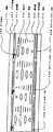
第1図は、本発明の実施例1の液晶表示素子の断面図であり、
第2図は、本発明の実施例1の液晶表示素子の電気光学特性を示す図であり、
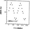
第3図は、本発明の実施例1の液晶表示素子の散乱指向性を示す図であり、
第4図は、本発明の実施例2の液晶表示素子の断面図であり、
第5図は、本発明の実施例3の液晶表示素子の断面図であり、
第6図は、比較例1の液晶表示素子の散乱指向性を示す図である。
実施例
(実施例1)
本実施例の液晶表示素子の断面図を第1図に示す。下側の基板108上には、クロムをスパッタリングにより約2000オングストローム形成後、パターニングされた反射画素電極107が形成されている。上側の基板101上には、ITO(Indium Tin Oxide)をスパッタリングにより約1500オングストローム形成後、パターニングされた透明画素電極102が形成されている。これら両基板108、101上には、ポリイミド配向膜(オプトマーAL1254;日本合成ゴム社製)が塗布、焼成されて形成された平行配向処理層106、103がそれぞれ設けられている。尚、液晶を基板表面近傍でランダムに平行配向させるため、ラビング処理は施されない。つづいて、2枚の基板を、空隙5μmにて、基板周囲を貼り合わせ、固定することにより、空パネルを得た。
次に、この空パネルに封入する、液晶及び高分子前駆体混合物について説明する。液晶としてTL−213(メルク社製)とMJ92786(メルク社製)を7:3で混合(以下液晶Aとする。)して用い、これにカイラル成分としてR1011(メルク社製)を、0.15重量%、二色性色素としてM361、SI−512、M137(すべて、三井東圧染料社製)を、それぞれ、1.0重量%、1.5重量%、0.4重量%混合して用いた。カイラル剤の添加量は、d/p(セル厚/液晶の捻れピッチ)=1/4、すなわち90゜ツイスト配向となるように決定した。また、高分子前駆体として、ビフェニルメタクリレートを、先の液晶混合物に対して7重量%用いた。以上を加熱混合して液晶状態とした後、先に説明した空パネルに真空封入した。つづいて、液晶性混合材料が等方相を示す温度以上に加熱処理した後、25℃へ急冷処理を行った。
パネルに封入された液晶性混合材料は、基板表面近傍にてランダムに平行配向し、基板101、108間で約90゜ツイストしている状態であることが偏光顕微鏡にて観察された。また、液晶性混合材料のランダムな配向による配向ドメインは、約1〜3μm程度で、均一にマルチドメイン化していることが観察された。
その後、パネルに、照度5mW/cm2(波長350nm)の紫外線を7分間照射して高分子を重合させることより、液晶性混合材料中から高分子を析出させて、第1図に示す本実施例の液晶表示素子を完成させた。液晶105は、紫外線照射前の配向状態を示していること、すなわち、基板表面近傍にてランダムに平行配向し、基板101、108間で約90゜ツイストしており、液晶のランダムな配向による配向ドメインは、約1〜3μm程度で、均一にマルチドメイン化していることが偏光顕微鏡により観察された。また、高分子104及び液晶105は、基板間にて互いに配向し、かつ分散した構造をとることも、偏光顕微鏡にて確認された。
第2図に、本実施例で得られた液晶表示素子の電気光学特性を示した。電気光学特性は閾特性を示し、電圧印加により反射率が増加するノーマリーブラック特性が得られた。すなわち、電圧オフ時で、二色性色素の吸収による黒表示が得られ、電圧を十分に印加した場合は、液晶105が電界方向に配向するので高分子と液晶との配向方向が異なるようになって媒体内で屈折率の不連続点が発生するために、光散乱状態となった。この時、二色性色素も電界方向に配向するので吸収が非常に小さくなり、白表示が得られた。
つづいて、本実施例の液晶表示素子の電気光学特性の測定結果を示す。電気光学特性は、キセノンランプリング光源を用い、液晶表示素子に100Hzの矩形波を印加して、表示素子表面の法線(パネル法線)方向から30゜傾いた方向(入射角30゜)から全方位(360゜)にわたって光を入射させて、入射光の法線方向への応答反射光を検出した。検出面積は、2mmφとした。反射率100%は、完全拡散表面の輝度にて規格化した。以下、閾電圧値V10は、(最大反射率−最小反射率)=100と規格化した際の反射率が10での電圧値、飽和電圧値V90は、反射率が90での電圧値で定義した。また、散乱指向性は、平行光線を使用して、平行光線とパネル法線のなす入射角ψとパネル回転角φとをパラメーターとして、パネル法線方向の反射率の変化を測定した。本実施例の液晶表示素子は、V10が1.9V、V90が3.4V、最大反射率が78%であった。また、第3図に、入射角ψを30゜とし、電圧3.8Vを印加した時の散乱指向性の測定結果を示した。
本実施例では、液晶と高分子が互いに配向分散した高分子分散液晶を用いた高分子分散型液晶表示素子において、大幅に駆動電圧が低下した。さらに、明るさの指標となる最大反射率が高く、良好な明るさとなった。また、本実施例の液晶表示素子は、第3図に示したように、パネルの回転角φに対する散乱指向性がない。したがって、ある方向からの光が強いような環境や、均一照明下において、パネルの配置方法による明るさの変化がなくなり、視角特性、携帯性、視認性が向上した。
(実施例2)
以下、本実施例では、画素電極毎に2端子素子(MIM)が形成され、液晶がマルチドメイン化され、かつ基板間でツイスト配向した構成を例示する。第4図に、本実施例の液晶表示素子の断面図を示した。下側の基板409を、2フォトプロセスにより製作されたMIM基板としている。基板工程では、Taをスパッタした後、所望の形状にパターニングし(フォト1工程目)、次にTaを陽極酸化し、Ta表面に絶縁膜Ta2O5を形成する。つづいて、Crをスパッタした後、所望の形状にパターニングして(フォト2工程目)、Ta−Ta2O5−Crより構成されるMIM素子407、およびCrからなる反射画素電極408が形成される。一方、上基板401には、ITOがスパッタされ、ストライプ状にパターニングされて、ITO電極402が形成される。つづいて、両基板上に、日本合成ゴム社製オプトマーAL1254をスピンコートした後、150℃にて1時間焼成して、平行配向処理層403、406を形成した。このようにして得られた2枚の基板を、空隙5μmにて、基板周囲を貼り合わせ、固定し、対角5インチの空パネルを作製した。尚、液晶の基板表面近傍でランダムに平行配向させるため、ラビング処理は施されない。
つづいて、実施例1と同じ液晶、二色性色素、カイラル剤および高分子前駆体からなる液晶性混合材料を上記の空パネルに真空注入した。パネルに封入された液晶性混合材料は、実施例1と同様に、偏光顕微鏡にて、基板表面近傍にて平行配向し、基板401、409間にて約90゜ツイストしている状態であることが観察され、また、液晶のランダムな配向による配向ドメインは、約1〜3μm程度で、均一にマルチドメイン化していることが観察された。
その後、パネルに、照度5mW/cm2(波長350nm)の紫外線を7分間照射して、液晶性混合材料中から高分子を析出させて、第4図に示す本実施例の液晶表示素子を完成させた。液晶405は、紫外線照射前の配向状態を示していること、すなわち、基板表面近傍にて平行配向し、基板401、409間にて約90゜ツイストしており、また、液晶のランダムな配向による配向ドメインは、約1〜3μm程度で、均一にマルチドメイン化していることが偏光顕微鏡で観察された。また、高分子404及び液晶405は基板間にて互いに配向し、かつ分散した構造をとることも、偏光顕微鏡にて確認された。
こうして得られた液晶表示素子を1/480デュティーにてMIM駆動したところ、実施例1の測定条件にて、最大反射率が63%、コントラストが11であった。また、電圧印加時の散乱の指向性がなく、携帯性、視覚特性、視認性に優れた液晶表示素子が得られた。さらに、この液晶表示素子の表面に、ノングレア処理と無反射コートを施すと、風景の写り込みが減少して視認性が極めて向上した。
なお、本実施例では、MIM基板上に反射電極を配置したが、対向基板側に反射電極を形成することも可能である。
(実施例3)
以下、本実施例では、画素電極毎に2端子素子(MIM)が形成され、また反射電極上にカラーフィルターが形成された基板を使用し、液晶がマルチドメイン化され、かつ基板間でツイスト配向した構成を例示する。第5図に、本実施例の液晶表示素子の断面図を示した。上側の基板501は、3フォトプロセスにより作製されたMIM基板としている。Taをスパッタした後、所望の形状にパターニングし(フォト1工程目)、次にTaを陽極酸化し、Ta表面に絶縁膜Ta2O5を形成する。つづいて、Crをスパッタした後、所望の形状にパターニングされ(フォト2工程目)、Crからなる配線及びTa−Ta2O5−Cr構成のMIM素子502が形成される。つづいて、ITOをスパッタした後、所望な形状にパターニングして(フォト3工程目)、MIM素子502にそれぞれ接続された透明画素電極503を形成する。一方、下基板510には、Al−Mgがスパッタされ、その後ストライプ状にパターニングされて反射電極509が形成される。この反射電極509上には、顔料カラーフィルター508(赤、緑、青)が画素毎にそれぞれ形成されている。つづいて、両基板に、日本合成ゴム社製オプトマーAL1254をスピンコートした後、150℃にて1時間焼成して、平行配向処理層504、507を形成した。このようにして得られた2枚の基板を、空隙5μmにて、基板周囲を貼り合わせ、固定し、対角5インチの空パネルを作製した。尚、液晶を基板表面近傍でランダムに平行配向させるため、ラビング処理は施されない。
つづいて、実施例1と同じ液晶、二色性色素、カイラル剤および高分子前駆体からなる液晶性混合材料を上記の空パネルに真空注入した。パネルに封入された液晶性混合材料は、実施例1と同様に、偏光顕微鏡にて、基板表面近傍にて平行配向し、基板501、510間にて約90゜ツイストしている状態であることが観察され、また、液晶のランダムな配向による配向ドメインは、約1〜3μm程度で、均一にマルチドメイン化していることが観察された。
その後、パネルに、照度5mW/cm2(波長350nm)の紫外線を7分間照射して、液晶中から高分子を析出させて、第5図に示す本実施例の液晶表示素子を完成させた。液晶506は、紫外線照射前の配向状態を示していること、すなわち、基板表面近傍にて平行配向し、基板501、510間にて約90゜ツイストしており、また、液晶のランダムな配向による配向ドメインは、約1〜3μm程度で、均一にマルチドメイン化していることが偏光顕微鏡で観察された。また、高分子505及び液晶506は、基板間にて互いに配向し、かつ分散した構造をとることも、偏光顕微鏡にて確認された。
こうして得られた液晶表示素子は、電圧オフ時で、二色性色素の吸収による黒表示が得られ、各カラー画素に電圧を印加することによりカラー表示が得られた。また、1/480デュティーにてMIM駆動したところ、実施例1の測定条件にて、最大反射率が32%、コントラストが12であった。また、8階調表示、512色表示が可能であった。さらに、電圧印加時の散乱の指向性がなく、携帯性、視覚特性、視認性の優れた液晶表示素子が得られた。さらに、この液晶表示素子の表面に、ノングレア処理と無反射コートを施すと、風景の写り込みが減少して視認性が極めて向上した。
なお、本実施例では、MIM基板に透明電極を配置したが、反射電極をMIM基板に配置し、その上にカラーフィルターを形成することも可能である。
また、本実施例で使用されるカラーフィルターの構成は、赤、緑、青に限定されず、自然色を再現できる構成であれば同様に使用することができる。また、カラーフィルターは、上基板側に配置することも可能である。
(比較例1)
以下、比較例として、マルチドメイン化されていない90゜ツイスト配向の構成を有する液晶表示素子を示す。具体的には、ポリイミド膜を一方向にラビング処理した配向膜を用い、上下基板でラビング方向が90゜になるように空パネルを作製した。用いた材料等は、実施例1と同様である。つづいて、実施例1に示した液晶性混合材料を封入し、照度5mW/cm2(波長350nm)の紫外線を7分間照射して、液晶中から高分子を析出させて、液晶表示素子を完成させた。実施例1と同様にして測定した散乱指向性の結果を第6図に示した。反射率は、光の入射方向により大きく変化し、強い散乱指向性を示した。
以上本発明の実施例を説明したが、本発明は上記実施例に限定されるものではない。
例えば、上記実施例1乃至3では、液晶に2色性色素を添加した構成としたが、もちろん無添加としてもよい。無添加の場合、電圧無印加時に黒レベルが若干上昇するものの、電圧印加時には色素の光吸収がなくなるために最大反射率が増加し、明るさが向上する。また、反射率の低い反射電極を使用した場合、あるいは、反射電極上に光吸収層を設けた場合は、特に2色性色素添加の必要はない。
また、上記実施例1乃至3では、ツイスト角90゜の構成について示したが、これに限定されない。ツイスト角は、好ましくは、360゜以下であり、特に好ましくは、30〜180゜である。ツイスト角0゜近傍では、ツイスト配向が安定せず、360゜を越えると、駆動電圧が高く、通常の非線形素子では駆動できない。
また、ツイスト角を決定するカイラル成分は、設定したd/p(セル厚/液晶の捻れピッチ)に応じて、最適量が添加される。カイラル剤は通常のTN、STNに使用されている材料が、そのまま好ましく使用できる。
基板表面近傍での、液晶のランダムな平行配向による配向ドメインは、電圧無印加時の均一性、電圧印加時の散乱性から、0.4〜10μmのサイズで均一形成されていることが望ましい。0.4μm未満では、散乱が弱く、10μm以上では、各配向ドメインが識別される。また、上記のようなサイズで、均一なマルチドメインを形成するには、液晶性混合材料を加熱し、等方相にした後、急冷する方法が好ましく使用できる。
上記実施例1乃至3では、平行配向処理に用いる配向膜として、ポリイミド膜を用いたが、他にポリアミド膜、SiO斜方蒸着膜、ポリビニルアルコール等が好ましく使用できる。
基板に使用される材料としては、ソーダガラス、石英、無アルカリガラス、シリコン単結晶、サファイア基板、熱硬化型高分子、熱可塑性高分子などが好ましく使用される。基板に使用される高分子材料は、基板間に挟持される液晶及び高分子に悪影響を及ぼさなければ特に制限されることはなく、PET、ポリエーテルスルホン、エポキシ硬化樹脂、フェノキシ樹脂、ポリアリルエーテル等が好ましく使用される。
反射電極は、実施例1および2ではCrとし、実施例3ではAl−Mgとしたが、Al、Cr、Mg、Ag、Au、Ptなどの金属単体、あるいはそれらの合金が好ましく使用できる。特に、安定性、反射率の点からCrあるいは、Al−Mg合金がより好ましく、Al−Mg合金の場合にはMgの添加量は0.1〜10重量%が望ましい。
液晶は、通常の液晶表示素子に使用されているものが好ましく使用できるが、散乱度を良好にするためには、液晶の複屈折率異方性△nが、0.15以上であることが望ましい。また、非線形素子で駆動するためには、液晶単体の比抵抗値が1.0×10⁹Ω・cm以上、特に好ましくは、1.0×10¹⁰Ω・cm以上であることが、保持率を高く保ち表示品質を良好にするためには望ましい。
2色性色素としては、通常のGH(ゲスト−ホスト)表示方式に使用されているアゾ系、アントラキノン系、ナフトキノン系、ペリレン系、キノフタロン系、アゾメチン系などが好ましく使用される。その中でも、耐光性の点からアントラキノン系単独、あるいは必要に応じて他の色素と混合したものが特に好ましい。これらの2色性色素は、必要な色によって、混合され使用される。
高分子前駆体としては、重合後、屈折率異方性を示し、液晶と配向分散するものであればなんでもよいが、液晶表示素子製造の簡便性から紫外線硬化型モノマーが望ましい。紫外線硬化型モノマーとしては、単官能メタクリレート、2官能メタクリレートあるいは多官能メタクリレートなどが好ましく使用される。散乱度を向上するために、これらモノマーは最低1個のベンゼン環をその分子構造中に含むことが望ましい。特に、ビフェニル、ターフェニル、クォーターフェニル骨格を含む材料が好ましく使用される。これらのモノマーには、カイラル性の成分を含むものでも良い。また、これらのモノマーは単独あるいは他のモノマーと混合した後、紫外線を照射して重合しても良い。
また、上記実施例2および3では、2端子の非線形素子としてMIM素子を使用したが、MIM素子以外に、ラテラル型MIM素子、バックトゥバック型MIM素子、MSI素子、ダイオードリング素子、バリスタ素子などが使用可能である。また、3端子非線形素子も、勿論使用でき、3端子非線形素子として、ポリシリコンTFT素子、アモルファスシリコンTFT素子、Cd−SeTFT素子などが使用可能である。
産業上の利用可能性
以上説明したように、本発明により、偏光板を不要とする明るく、ダブルイメージのない高分子分散型液晶表示素子において、特に、従来問題となっていた駆動電圧、散乱指向性による視認性の問題点を、液晶をマルチドメイン化し、かつツイスト配向状態とする新規な構成により、解決することが可能となった。
とくに、本発明の液晶表示素子の駆動電圧は、TNモードなみにまで低減できたため、MIM素子、TFT素子にて、十分に駆動することが可能となり、明るさ、コントラストを大幅に向上することが可能となった。このことにより、反射型カラー液晶表示素子とした場合の表示色数、視認性を向上することが可能となった。また、高耐圧ドライバーの必要性がなくなり、消費電力、コストを低減できた。
さらに、本発明の液晶表示素子では、散乱指向性を抑えることにより、明るさ、視覚特性、視認性が向上した。
その結果、本発明は、多様な環境が想定される携帯用途に適した液晶表示素子に利用できる。また、本発明は、アクティブマトリクス駆動であり、低消費電力、かつ表示品質の優れた反射型大容量ディスプレイに利用できる。TECHNICAL FIELD The present invention relates to a liquid crystal display element and a manufacturing method thereof, and more particularly to a liquid crystal display element constituting a display unit of an information equipment terminal, a television, a home appliance, and the like and a manufacturing method thereof.
Background Art In recent years, information devices have been reduced in size and weight, and displays mounted thereon are also required to save power. A liquid crystal display element using a TN mode is used for a small display capacity device, and a liquid crystal display element using an FTN mode is used as a reflective display for a medium display capacity device. Furthermore, the application of combining an information input device such as a tablet on a reflective display has been expanded, and the reflective liquid crystal display element is required to have good brightness and visibility.
However, TN and FTN liquid crystal display elements that use conventional polarizing plates have low light utilization efficiency, so they become dark when they are of the reflective type, and they are extremely dark when combined with an information input device such as a tablet. It was an issue. In addition, when the reflective type is the TN method or FTN method, the reflector is placed over the polarizing plate on the back side of the backside of the substrate, so there is a double image of the display, fine characters are unclear, and visibility is a problem. It was.
On the other hand, recently, bright reflective displays that do not use polarizing plates are being developed. For example, liquid crystal display elements (such as Japanese Examined Patent Publication No. Sho 58-501631) that are controlled to be transparent when an electric field is applied and light scattering when no electric field is applied, using a polymer-dispersed liquid crystal in which liquid crystal and polymer are dispersed, Liquid crystal display elements (EPO488116A2, European Patent Laid-Open No. 4-227684, Japanese Patent Laid-Open No. 5-119302, etc.) that are controlled to be scattered, transparent when no electric field is applied, or light absorption have been developed.
A polymer-dispersed liquid crystal display element using a polymer-dispersed liquid crystal in which liquid crystal and polymer are aligned and dispersed with each other disclosed in this European published patent EPO488116A2 and the like does not use a polarizing plate, thus producing a bright reflective display Is possible. Furthermore, since a polarizing plate is not used, the pixel electrode can also be used as a light reflecting surface. In this case, a bright reflective display without a double image of display can be realized.
However, the conventional technology developed for a polymer dispersed liquid crystal display element using a polymer dispersed liquid crystal in which liquid crystal and polymer are aligned and dispersed can solve the problem of a liquid crystal display element using a polarizing plate. In order to obtain the scattering characteristics and ensure the brightness, it is necessary to twist the liquid crystal by 360 ° or more. As a result, there is a problem that the driving voltage becomes high.
For example, large-capacity display is possible by forming active elements such as TFT (Thin Film Transistor) and MIM (Metal-Insulator-Metal) elements for each pixel and controlling the electrical signal for each pixel. Since the driving voltage of the dispersed liquid crystal is high, it is difficult to drive the liquid crystal so that it responds sufficiently from the viewpoint of the breakdown voltage of the active element, which causes a reduction in contrast ratio, and also requires a high breakdown voltage driving driver. There was a problem.
In addition, there is a problem that directivity exists in scattering due to the structure of orientation dispersion. This directivity means that the light scattering efficiency changes depending on the direction of the external incident light. For example, the brightness changes when the panel is rotated, and the visibility is easily affected by the usage environment. . This directivity increases as the twist of the liquid crystal decreases. Accordingly, in order to solve this problem, the twist of the liquid crystal may be increased. However, since the drive voltage becomes high in that case, it is impossible to increase the twist from the viewpoint of the drive voltage.
Furthermore, when a large amount of a chiral agent is added to generate a large twisting force, there is a problem that hysteresis occurs in electro-optical characteristics.
The present invention has been made to solve such a problem, and the object of the present invention is to control a liquid crystal that is aligned and dispersed with each other in a novel alignment state, thereby reducing a low voltage. An object of the present invention is to provide a liquid crystal display element that can be driven, is bright, has a high contrast ratio, has improved scattering directivity, and is less dependent on the use environment in terms of visibility, and a method for manufacturing the same.
DISCLOSURE OF THE INVENTION In order to solve the above-mentioned problems, a liquid crystal display element of the present invention comprises a liquid crystal and a polymer-dispersed liquid crystal containing a polymer having refractive index anisotropy sandwiched between two substrates on which an alignment film is formed. In the liquid crystal display element, the polymer dispersed liquid crystal is sandwiched between electrodes and includes a dichroic dye, and the liquid crystal is substantially parallel to the surface of the substrate in the vicinity of the surface of the substrate. A plurality of domains that are aligned and have a size of 0.4 to 10 μm, and the alignment directions of the liquid crystals in the plurality of domains are each in a random direction within a plane parallel to the substrate surface, and the substrate When the electric field is applied between the electrodes, the liquid crystal and the dichroic dye are aligned in the direction of the electric field, and the polymer and the liquid crystal are different from each other. The light is scattered in a direction oriented in a certain direction, and when an electric field is not applied between the electrodes, the light is absorbed by light absorption of the dichroic dye.
Thus, although the liquid crystal is twisted between the substrates, the directivity of scattering is lost because the liquid crystal is randomly aligned near the substrate surface and almost parallel to the substrate surface. Therefore, it is not necessary to increase the twist of the liquid crystal in order to solve the directivity problem, and as a result, it can be driven with a small voltage. Further, it is not necessary to add a large amount of chiral agent in order to increase the twist of the liquid crystal, and as a result, the occurrence of hysteresis in the electro-optical characteristics is suppressed.
The alignment treatment on the substrate surface is preferably performed by forming an alignment film on the substrate surface.
The domain is formed by heat-treating the polymer-dispersed liquid crystal at a temperature equal to or higher than an isotropic phase and then rapidly cooling, and the alignment film is preferably not rubbed.
The liquid crystal display element of the present invention has a plurality of domains in a plane in which the liquid crystal is parallel to the substrate surface, and each domain exists in an irregular direction in a plane parallel to the substrate surface. The liquid crystal in each domain is twisted.
In this case, the size of each domain is preferably about 0.4 to 10 μm. If it is less than 0.4 μm, scattering is weak, and if it exceeds 10 μm, each orientation domain is identified.
The twist angle of the liquid crystal is preferably 360 ° or less. If it exceeds 360 °, the drive voltage becomes too high and it cannot be driven by a normal nonlinear element. The twist angle of the liquid crystal is particularly preferably 30 to 180 °.
Moreover, it is preferable that the liquid crystal contains a chiral agent.
Furthermore, it is preferable that one of the electrodes is formed of a reflective material, and the present invention is preferably applied to a reflective liquid crystal display element.
According to the method for manufacturing a liquid crystal display element of the present invention, a step of forming a first electrode on a first substrate and a second electrode on a second substrate; A step of forming an empty panel by laminating the substrate, a step of arranging a liquid crystal mixed material of a polymer or a polymer precursor and a liquid crystal composition in the empty panel, and a polymer from the liquid crystal mixed material. And a step of phase separation of the liquid crystal and the polymer.
In this way, alignment films are formed on the surfaces of the first and second substrates, respectively, and an empty panel is formed by the first substrate and the second substrate without rubbing the surfaces of the first and second substrates. And a liquid crystalline mixed material of a polymer or a polymer precursor and a liquid crystal composition is disposed between the first and second substrates of the empty panel, so that the liquid crystalline mixed material becomes the first and second liquid crystalline mixed materials. Twist alignment is performed between the second substrates, but in the vicinity of the substrate surface, it is randomly aligned substantially parallel to the substrate surface. After that, by depositing a polymer from the liquid crystalline mixed material and phase-separating the liquid crystal and the polymer, the alignment state of the liquid crystal can be maintained in the alignment state of the liquid crystalline mixed material before the phase separation. Is twist-oriented between the first and second substrates, but can be randomly oriented almost parallel to the substrate surface in the vicinity of the substrate surface.
In this case, after arranging the liquid crystalline mixed material in the empty panel, the liquid crystalline mixed material is heated to a temperature at which the liquid crystalline mixed material is isotropic, and then rapidly cooled, whereby a plurality of domains can be formed in an appropriate size.
In addition, using an ultraviolet curable monomer as a polymer precursor, polymerizing the monomer by irradiating the liquid crystalline mixed material with ultraviolet rays to precipitate the polymer to phase-separate the liquid crystal and the polymer, This is preferable from the standpoint of manufacturing a liquid crystal display element.
[Brief description of the drawings]
FIG. 1 is a cross-sectional view of a liquid crystal display element of Example 1 of the present invention,
FIG. 2 is a diagram showing electro-optical characteristics of the liquid crystal display element of Example 1 of the present invention,
FIG. 3 is a diagram showing the scattering directivity of the liquid crystal display element of Example 1 of the present invention,
FIG. 4 is a cross-sectional view of the liquid crystal display element of Example 2 of the present invention,
FIG. 5 is a cross-sectional view of the liquid crystal display element of Example 3 of the present invention,
FIG. 6 is a diagram showing the scattering directivity of the liquid crystal display element of Comparative Example 1.
Example (Example 1)
FIG. 1 shows a cross-sectional view of the liquid crystal display element of this example. On the lower substrate 108, a reflective pixel electrode 107 is formed which is formed by sputtering about 2000 Å of chromium by sputtering. On the upper substrate 101, a
Next, the liquid crystal and polymer precursor mixture sealed in the empty panel will be described. TL-213 (manufactured by Merck) and MJ92786 (manufactured by Merck) were mixed at a ratio of 7: 3 (hereinafter referred to as liquid crystal A) as the liquid crystal, and R1011 (manufactured by Merck) was used as the chiral component. %, M361, SI-512, and M137 (all manufactured by Mitsui Toatsu Dye Co., Ltd.) were mixed as 1.0% by weight, 1.5% by weight, and 0.4% by weight, respectively. The addition amount of the chiral agent was determined so that d / p (cell thickness / liquid crystal twist pitch) = 1/4, that is, 90 ° twist alignment. Further, 7% by weight of biphenyl methacrylate was used as a polymer precursor with respect to the liquid crystal mixture. The above was heated and mixed to obtain a liquid crystal state, and then vacuum-sealed in the empty panel described above. Subsequently, after the heat treatment was performed at a temperature higher than the temperature at which the liquid crystalline mixed material exhibited an isotropic phase, a rapid cooling treatment was performed to 25 ° C.
It was observed with a polarizing microscope that the liquid crystalline mixed material sealed in the panel was randomly aligned parallel to the vicinity of the substrate surface and twisted about 90 ° between the substrates 101 and 108. In addition, it was observed that the alignment domain due to the random alignment of the liquid crystalline mixed material was about 1 to 3 μm and was uniformly multi-domained.
After that, the polymer is polymerized by irradiating the panel with ultraviolet light having an illuminance of 5 mW / cm2 (wavelength 350 nm) for 7 minutes to polymerize the polymer, and this embodiment shown in FIG. 1 is performed. An example liquid crystal display element was completed. The liquid crystal 105 shows the alignment state before ultraviolet irradiation, that is, the liquid crystal 105 is randomly aligned in the vicinity of the substrate surface and twisted by about 90 ° between the substrates 101 and 108. It was observed with a polarization microscope that the domains were about 1 to 3 μm and were uniformly multidomained. It was also confirmed with a polarizing microscope that the
FIG. 2 shows the electro-optical characteristics of the liquid crystal display element obtained in this example. The electro-optical characteristic showed a threshold characteristic, and a normally black characteristic in which the reflectance increased with voltage application was obtained. That is, when the voltage is off, a black display is obtained by absorption of the dichroic dye, and when the voltage is sufficiently applied, the liquid crystal 105 is aligned in the electric field direction so that the alignment direction of the polymer and the liquid crystal is different. As a result, discontinuous points of the refractive index are generated in the medium, resulting in a light scattering state. At this time, since the dichroic dye was also oriented in the electric field direction, the absorption was very small and a white display was obtained.
Next, measurement results of electro-optical characteristics of the liquid crystal display element of this example will be shown. The electro-optical characteristics are as follows. Using a xenon lamp ring light source, applying a 100 Hz rectangular wave to the liquid crystal display element, tilting 30 ° from the normal (panel normal) direction of the display element surface (incident angle 30 °) Light was incident in all directions (360 °), and response reflected light in the normal direction of the incident light was detected. The detection area was 2 mmφ. The reflectance of 100% was normalized by the brightness of the completely diffusing surface. Hereinafter, the threshold voltage value V10 is defined as the voltage value when the reflectance is 10 when normalized as (maximum reflectance−minimum reflectance) = 100, and the saturation voltage value V90 is defined as the voltage value when the reflectance is 90 did. Further, the scattering directivity was measured by using a parallel light beam and measuring the change in reflectance in the panel normal direction using the incident angle ψ and the panel rotation angle φ formed by the parallel light beam and the panel normal as parameters. In the liquid crystal display element of this example, V10 was 1.9 V, V90 was 3.4 V, and the maximum reflectance was 78%. FIG. 3 shows the measurement results of the scattering directivity when the incident angle ψ is 30 ° and a voltage of 3.8 V is applied.
In this example, in the polymer dispersion type liquid crystal display element using the polymer dispersion liquid crystal in which the liquid crystal and the polymer are aligned and dispersed with each other, the driving voltage is greatly reduced. Furthermore, the maximum reflectivity as an index of brightness was high, and the brightness was favorable. Further, as shown in FIG. 3, the liquid crystal display element of this example does not have scattering directivity with respect to the rotation angle φ of the panel. Therefore, in an environment where the light from a certain direction is strong or under uniform illumination, there is no change in brightness due to the panel arrangement method, and viewing angle characteristics, portability, and visibility are improved.
(Example 2)
Hereinafter, in this embodiment, a configuration in which a two-terminal element (MIM) is formed for each pixel electrode, the liquid crystal is multi-domained, and twisted between substrates is exemplified. FIG. 4 shows a cross-sectional view of the liquid crystal display element of this example. The lower substrate 409 is an MIM substrate manufactured by a two-photo process. In the substrate process, Ta is sputtered and then patterned into a desired shape (first photo process), and then Ta is anodized to form an insulating film Ta2 O5 on the Ta surface. Subsequently, Cr is sputtered, and then patterned into a desired shape (second photo process) to form a MIM element 407 composed of Ta—Ta2 O5 —Cr, and a reflective pixel electrode 408 composed of Cr. The On the other hand, ITO is sputtered on the upper substrate 401 and patterned in a stripe shape to form an
Subsequently, a liquid crystal mixed material composed of the same liquid crystal, dichroic dye, chiral agent and polymer precursor as in Example 1 was vacuum-injected into the above empty panel. The liquid crystalline mixed material sealed in the panel is in the state of being aligned in parallel in the vicinity of the substrate surface and twisted by about 90 ° between the substrates 401 and 409 in the same manner as in the first embodiment. Further, it was observed that the alignment domain due to the random alignment of the liquid crystal was about 1 to 3 μm and was uniformly multi-domained.
After that, the panel is irradiated with ultraviolet rays having an illuminance of 5 mW / cm2 (wavelength 350 nm) for 7 minutes to deposit a polymer from the liquid crystalline mixed material, thereby completing the liquid crystal display element of this embodiment shown in FIG. I let you. The liquid crystal 405 shows the alignment state before ultraviolet irradiation, that is, parallel alignment in the vicinity of the substrate surface, twisted by about 90 ° between the substrates 401 and 409, and due to the random alignment of the liquid crystal The alignment domain was about 1 to 3 μm, and it was observed with a polarizing microscope that it was uniformly multidomained. It was also confirmed by a polarizing microscope that the polymer 404 and the liquid crystal 405 had a structure in which they were aligned with each other and dispersed between the substrates.
When the liquid crystal display element thus obtained was MIM driven at 1/480 duty, the maximum reflectance was 63% and the contrast was 11 under the measurement conditions of Example 1. In addition, a liquid crystal display element having no scattering directivity during voltage application and excellent portability, visual characteristics, and visibility was obtained. Furthermore, when non-glare treatment and non-reflective coating were applied to the surface of the liquid crystal display element, the reflection of the scenery was reduced and the visibility was greatly improved.
In this embodiment, the reflective electrode is arranged on the MIM substrate, but it is also possible to form the reflective electrode on the counter substrate side.
(Example 3)
Hereinafter, in this embodiment, a substrate in which a two-terminal element (MIM) is formed for each pixel electrode and a color filter is formed on a reflective electrode is used, the liquid crystal is multi-domained, and twist alignment is performed between the substrates. An example of the configuration is shown. FIG. 5 shows a cross-sectional view of the liquid crystal display element of this example. The
Subsequently, a liquid crystal mixed material composed of the same liquid crystal, dichroic dye, chiral agent and polymer precursor as in Example 1 was vacuum-injected into the above empty panel. The liquid crystal mixed material sealed in the panel is in a state of being aligned in parallel near the substrate surface and twisted by about 90 ° between the
Thereafter, the panel was irradiated with ultraviolet rays having an illuminance of 5 mW / cm2 (wavelength 350 nm) for 7 minutes to precipitate a polymer from the liquid crystal, thereby completing the liquid crystal display element of this example shown in FIG. The
The liquid crystal display element thus obtained was able to obtain a black display by absorption of a dichroic dye when the voltage was turned off, and a color display was obtained by applying a voltage to each color pixel. When MIM driving was performed at 1/480 duty, the maximum reflectance was 32% and the contrast was 12 under the measurement conditions of Example 1. In addition, 8-tone display and 512-color display were possible. Further, a liquid crystal display element having no scattering directivity when voltage was applied and having excellent portability, visual characteristics, and visibility was obtained. Furthermore, when non-glare treatment and non-reflective coating were applied to the surface of the liquid crystal display element, the reflection of the scenery was reduced and the visibility was greatly improved.
In this embodiment, the transparent electrode is disposed on the MIM substrate, but it is also possible to dispose the reflective electrode on the MIM substrate and form a color filter thereon.
The configuration of the color filter used in this embodiment is not limited to red, green, and blue, and any configuration that can reproduce a natural color can be used similarly. The color filter can also be disposed on the upper substrate side.
(Comparative Example 1)
Hereinafter, as a comparative example, a liquid crystal display element having a configuration of 90 ° twist alignment that is not multi-domained is shown. Specifically, an empty panel was produced using an alignment film obtained by rubbing a polyimide film in one direction so that the rubbing direction was 90 ° between the upper and lower substrates. The materials used were the same as in Example 1. Next, the liquid crystal mixed material shown in Example 1 was sealed, and ultraviolet rays having an illuminance of 5 mW / cm2 (wavelength 350 nm) were irradiated for 7 minutes to precipitate a polymer from the liquid crystal, thereby completing a liquid crystal display device. I let you. The result of the scattering directivity measured in the same manner as in Example 1 is shown in FIG. The reflectivity changed greatly depending on the incident direction of light, and showed strong scattering directivity.
As mentioned above, although the Example of this invention was described, this invention is not limited to the said Example.
For example, in Examples 1 to 3 described above, the dichroic dye is added to the liquid crystal. In the case of no addition, the black level slightly increases when no voltage is applied, but the maximum reflectance is increased and the brightness is improved because the light absorption of the dye is lost when the voltage is applied. In addition, when a reflective electrode having a low reflectance is used, or when a light absorption layer is provided on the reflective electrode, it is not particularly necessary to add a dichroic dye.
In the first to third embodiments, the configuration with a twist angle of 90 ° is shown, but the present invention is not limited to this. The twist angle is preferably 360 ° or less, particularly preferably 30 to 180 °. In the vicinity of the twist angle of 0 °, the twist orientation is not stable. When the twist angle exceeds 360 °, the drive voltage is high, and it cannot be driven by a normal nonlinear element.
Further, an optimum amount of the chiral component that determines the twist angle is added according to the set d / p (cell thickness / twist pitch of liquid crystal). As the chiral agent, materials used in ordinary TN and STN can be preferably used as they are.
In the vicinity of the substrate surface, the alignment domain by random parallel alignment of the liquid crystal is desirably formed uniformly in a size of 0.4 to 10 μm from the uniformity when no voltage is applied and the scattering property when a voltage is applied. Below 0.4 μm, scattering is weak, and above 10 μm, each orientation domain is identified. In order to form a uniform multi-domain with the above size, a method in which the liquid crystalline mixed material is heated to an isotropic phase and then rapidly cooled can be preferably used.
In Examples 1 to 3, a polyimide film was used as the alignment film used for the parallel alignment treatment, but a polyamide film, a SiO oblique deposition film, polyvinyl alcohol, or the like can be preferably used.
As a material used for the substrate, soda glass, quartz, alkali-free glass, silicon single crystal, sapphire substrate, thermosetting polymer, thermoplastic polymer, and the like are preferably used. The polymer material used for the substrate is not particularly limited as long as it does not adversely affect the liquid crystal and the polymer sandwiched between the substrates. PET, polyethersulfone, epoxy cured resin, phenoxy resin, polyallyl ether Etc. are preferably used.
The reflective electrode is Cr in Examples 1 and 2, and Al—Mg in Example 3. However, simple metals such as Al, Cr, Mg, Ag, Au, and Pt, or alloys thereof can be preferably used. In particular, Cr or an Al—Mg alloy is more preferable from the viewpoint of stability and reflectance. In the case of an Al—Mg alloy, the amount of Mg added is preferably 0.1 to 10% by weight.
As the liquid crystal, those used in ordinary liquid crystal display elements can be preferably used, but in order to improve the degree of scattering, it is desirable that the birefringence anisotropy Δn of the liquid crystal is 0.15 or more. In order to drive with a non-linear element, the specific resistance value of the liquid crystal alone is 1.0 × 10⁹ Ω · cm or more, particularly preferably 1.0 × 10¹⁰ Ω · cm or more. Desirable for good quality.
As the dichroic dye, azo, anthraquinone, naphthoquinone, perylene, quinophthalone, azomethine, and the like used in a normal GH (guest-host) display system are preferably used. Among these, from the viewpoint of light resistance, anthraquinone type alone or a mixture with other dyes as required is particularly preferable. These dichroic dyes are mixed and used depending on the required color.
Any polymer precursor may be used as long as it exhibits refractive index anisotropy after polymerization and is oriented and dispersed with liquid crystal. However, an ultraviolet curable monomer is desirable from the viewpoint of simplicity of manufacturing a liquid crystal display element. As the ultraviolet curable monomer, monofunctional methacrylate, bifunctional methacrylate or polyfunctional methacrylate is preferably used. In order to improve the degree of scattering, these monomers preferably contain at least one benzene ring in their molecular structure. In particular, a material containing a biphenyl, terphenyl, or quarterphenyl skeleton is preferably used. These monomers may contain a chiral component. Further, these monomers may be polymerized by irradiating them with ultraviolet light alone or after mixing with other monomers.
In Examples 2 and 3, the MIM element is used as the two-terminal nonlinear element. In addition to the MIM element, a lateral MIM element, a back-to-back MIM element, an MSI element, a diode ring element, a varistor element, etc. It can be used. Of course, a three-terminal nonlinear element can also be used. As the three-terminal nonlinear element, a polysilicon TFT element, an amorphous silicon TFT element, a Cd-Se TFT element, or the like can be used.
INDUSTRIAL APPLICABILITY As described above, according to the present invention, a bright and double image-free polymer dispersed liquid crystal display element that does not require a polarizing plate is particularly problematic in the conventional driving voltage and scattering directivity. The problem of visibility due to the property can be solved by a novel configuration in which the liquid crystal is multi-domain and is in a twist alignment state.
In particular, the driving voltage of the liquid crystal display element of the present invention can be reduced to the level of the TN mode, so that it can be driven sufficiently by the MIM element and TFT element, and the brightness and contrast can be greatly improved. It has become possible. This makes it possible to improve the number of display colors and the visibility when a reflective color liquid crystal display element is used. In addition, the need for a high-voltage driver has been eliminated, reducing power consumption and cost.
Furthermore, in the liquid crystal display element of the present invention, brightness, visual characteristics, and visibility are improved by suppressing the scattering directivity.
As a result, the present invention can be used for a liquid crystal display element suitable for portable use in various environments. Further, the present invention is active matrix driving, and can be used for a reflective large-capacity display with low power consumption and excellent display quality.
Claims (2)
Translated fromJapanese前記高分子分散液晶は電極間に挟まれているとともに二色性色素を含み、
前記液晶は、前記基板の表面近傍において、前記基板の表面に対してほぼ平行に配向し、かつ0.4〜10μmの大きさのドメインとして複数形成されてなるとともに、複数の前記ドメインにおける前記液晶の配向方向は、前記基板表面に平行な面内において各々ランダムな方向を向き、前記基板間においてはツイスト配向しており、
前記電極間に電界を印加したときには、前記液晶及び前記二色性色素が電界方向に配向するとともに前記高分子と前記液晶とが互いに異なる方向に配向して光散乱状態となり、
前記電極間に電界を印加しないときには、前記二色性色素の光吸収による光吸収状態となることを特徴とする液晶表示素子。In a liquid crystal display element in which a polymer dispersed liquid crystal containing a liquid crystal and a polymer having refractive index anisotropy is sandwiched between two substrates on which an alignment film is formed,
The polymer dispersed liquid crystal is sandwiched between electrodes and includes a dichroic dye,
In the vicinity of the surface of the substrate, the liquid crystal is aligned substantially parallel to the surface of the substrate and is formed as a plurality of domains having a size of 0.4 to 10 μm, and the alignment of the liquid crystal in the plurality of domains The direction is a random direction in a plane parallel to the substrate surface, and is twist-oriented between the substrates,
When an electric field is applied between the electrodes, the liquid crystal and the dichroic dye are aligned in the direction of the electric field, and the polymer and the liquid crystal are aligned in different directions, and are in a light scattering state.
A liquid crystal display element, wherein when an electric field is not applied between the electrodes, a light absorption state is obtained by light absorption of the dichroic dye.
Applications Claiming Priority (2)
| Application Number | Priority Date | Filing Date | Title |
|---|---|---|---|
| JP29843994 | 1994-12-01 | ||
| PCT/JP1995/002461WO1996017272A1 (en) | 1994-12-01 | 1995-12-01 | Liquid crystal display element and method of manufacturing the same |
Publications (1)
| Publication Number | Publication Date |
|---|---|
| JP3659975B2true JP3659975B2 (en) | 2005-06-15 |
Family
ID=17859729
Family Applications (1)
| Application Number | Title | Priority Date | Filing Date |
|---|---|---|---|
| JP51859296AExpired - LifetimeJP3659975B2 (en) | 1994-12-01 | 1995-12-01 | Liquid crystal display element and manufacturing method thereof |
Country Status (5)
| Country | Link |
|---|---|
| US (1) | US6025895A (en) |
| EP (1) | EP0749030A4 (en) |
| JP (1) | JP3659975B2 (en) |
| TW (1) | TW355228B (en) |
| WO (1) | WO1996017272A1 (en) |
Families Citing this family (15)
| Publication number | Priority date | Publication date | Assignee | Title |
|---|---|---|---|---|
| JPH1073815A (en)* | 1996-06-19 | 1998-03-17 | Seiko Instr Inc | Reflection type liquid crystal display device |
| KR19990076932A (en)* | 1996-10-25 | 1999-10-25 | 요트.게.아. 롤페즈 | Plasma-addressed liquid crystal display device with reduced column voltage |
| WO1999031545A1 (en)* | 1997-12-17 | 1999-06-24 | Matsushita Electric Industrial Co., Ltd. | Polymer dispersion type liquid crystal display panel and its manufacturing method |
| FR2779839B1 (en)* | 1998-06-10 | 2003-06-06 | Saint Gobain Vitrage | ELECTRICALLY CONTROLLED SYSTEM WITH VARIABLE OPTICAL PROPERTIES |
| US6449028B1 (en)* | 1998-06-12 | 2002-09-10 | Asulab S.A. | Liquid crystal display device having sealing frame and/or spacers formed of anisotropic polymer used to align the liquid crystal molecules |
| CN1279395C (en)* | 1998-08-26 | 2006-10-11 | 日产化学工业株式会社 | Liquid crystal aligning agent, liquid crystal cell using the same, and method for aligning liquid crystal |
| JP2000162581A (en)* | 1998-12-01 | 2000-06-16 | Sharp Corp | Reflection type liquid crystal display device and manufacturing method thereof |
| JP3497098B2 (en)* | 1999-05-25 | 2004-02-16 | シャープ株式会社 | Liquid crystal display device |
| GB9928126D0 (en) | 1999-11-30 | 2000-01-26 | Secr Defence | Bistable nematic liquid crystal device |
| WO2003046651A1 (en)* | 2001-11-28 | 2003-06-05 | Koninklijke Philips Electronics N.V. | Colour liquid crystal display device |
| US7274413B1 (en)* | 2002-12-06 | 2007-09-25 | United States Of America As Represented By The Secretary Of The Navy | Flexible video display apparatus and method |
| JP2014021140A (en)* | 2012-07-12 | 2014-02-03 | Seiko Epson Corp | Screen and image display system |
| CN102967962B (en)* | 2012-11-26 | 2015-01-14 | 京东方科技集团股份有限公司 | Transparent polymer dispersed liquid crystal display device and manufacturing method and application thereof |
| CN114063337B (en)* | 2020-08-07 | 2024-01-26 | 马耀东 | Epitaxial alignment liquid crystal display |
| PL445711A1 (en)* | 2023-07-30 | 2025-02-03 | Uniwersytet Warszawski | Method for controlling domains of organic compounds exhibiting conformational chirality |
Family Cites Families (16)
| Publication number | Priority date | Publication date | Assignee | Title |
|---|---|---|---|---|
| US4435047A (en)* | 1981-09-16 | 1984-03-06 | Manchester R & D Partnership | Encapsulated liquid crystal and method |
| JPS62174725A (en)* | 1985-09-27 | 1987-07-31 | Sanyo Electric Co Ltd | Liquid crystal display device |
| NL9000808A (en)* | 1990-04-06 | 1991-11-01 | Koninkl Philips Electronics Nv | LIQUID CRYSTALLINE MATERIAL AND IMAGE DISPLAY CELL CONTAINING THIS MATERIAL. |
| JP3060656B2 (en)* | 1990-11-26 | 2000-07-10 | セイコーエプソン株式会社 | Liquid crystal display device |
| JP2801102B2 (en)* | 1991-02-01 | 1998-09-21 | 富士通株式会社 | Liquid crystal display |
| KR940003349Y1 (en)* | 1991-08-24 | 1994-05-23 | 삼성전관 주식회사 | Device for lighting liquid crystal display devices |
| JPH05100213A (en)* | 1991-10-08 | 1993-04-23 | Toshiba Corp | Liquid crystal display element |
| US5394255A (en)* | 1992-01-27 | 1995-02-28 | Sekisui Kagaku Kogyo Kabushiki Kaisha | Liquid crystal display using a plurality of light adjusting sheets angled at 5 degrees or more |
| US5528720A (en)* | 1992-03-23 | 1996-06-18 | Minnesota Mining And Manufacturing Co. | Tapered multilayer luminaire devices |
| US5237641A (en)* | 1992-03-23 | 1993-08-17 | Nioptics Corporation | Tapered multilayer luminaire devices |
| JP3006306B2 (en)* | 1992-09-16 | 2000-02-07 | インターナショナル・ビジネス・マシーンズ・コーポレイション | Optical film and liquid crystal display device using the optical film |
| KR100225234B1 (en)* | 1992-09-24 | 1999-10-15 | 손욱 | Cholesteric lc material and pdlc element |
| US5739889A (en)* | 1993-04-27 | 1998-04-14 | Sharp Kabushiki Kaisha | Liquid crystal display device and a production method for the same |
| JPH07152024A (en)* | 1993-05-17 | 1995-06-16 | Sharp Corp | Liquid crystal display element |
| US5530573A (en)* | 1993-05-27 | 1996-06-25 | Sharp Kabushiki Kaisha | Multiple domain liquid crystal display having a cell thickness divided by helical pitch equal to 1/8 or less |
| US5600455A (en)* | 1994-08-31 | 1997-02-04 | Enplas Corporation | Prismatic member with coarsened portions or triangular prismatic and semi-circular prismatic members arranged on a flat light emitting surface |
- 1995
- 1995-12-01JPJP51859296Apatent/JP3659975B2/ennot_activeExpired - Lifetime
- 1995-12-01USUS08/687,342patent/US6025895A/ennot_activeExpired - Lifetime
- 1995-12-01EPEP95938628Apatent/EP0749030A4/ennot_activeWithdrawn
- 1995-12-01WOPCT/JP1995/002461patent/WO1996017272A1/ennot_activeApplication Discontinuation
- 1995-12-21TWTW084113715Apatent/TW355228B/ennot_activeIP Right Cessation
Also Published As
| Publication number | Publication date |
|---|---|
| TW355228B (en) | 1999-04-01 |
| EP0749030A4 (en) | 1998-03-18 |
| WO1996017272A1 (en) | 1996-06-06 |
| EP0749030A1 (en) | 1996-12-18 |
| US6025895A (en) | 2000-02-15 |
Similar Documents
| Publication | Publication Date | Title |
|---|---|---|
| JP3060656B2 (en) | Liquid crystal display device | |
| US5680185A (en) | Polymer dispersed liquid crystal (PDLC) display apparatus | |
| JP3659975B2 (en) | Liquid crystal display element and manufacturing method thereof | |
| JP3651004B2 (en) | Liquid crystal display element, manufacturing method thereof, and electronic apparatus | |
| JP3310569B2 (en) | Reflective liquid crystal display | |
| JP2000066195A (en) | Reflective liquid crystal display | |
| JP3416947B2 (en) | Liquid crystal display device and method of manufacturing the same | |
| JP3298522B2 (en) | Liquid crystal display device | |
| JPH08106087A (en) | Reflection type liquid crystal display device | |
| WO1996017273A1 (en) | Liquid crystal display element and method of manufacturing the same | |
| JPH1164895A (en) | Reflection type liquid crystal color display device | |
| JP3862473B2 (en) | Liquid crystal element, liquid crystal functional material, and liquid crystal device | |
| JPH08211369A (en) | Liquid crystal display element | |
| JP3586779B2 (en) | Ferroelectric liquid crystal display | |
| JP3795608B2 (en) | Reflective guest-host type liquid crystal display device | |
| JPH08114797A (en) | Reflective liquid crystal display device and manufacturing method thereof | |
| JP3219733B2 (en) | Reflective liquid crystal display | |
| JP3569296B2 (en) | Liquid crystal electro-optical element | |
| JPH06186541A (en) | Display element and manufacturing method thereof | |
| JPH0749502A (en) | Liquid crystal display element | |
| JPH0743730A (en) | Liquid crystal display element | |
| JPH0798453A (en) | Liquid crystal display device and information processing device using the same | |
| JPH0743741A (en) | Liquid crystal display element | |
| JPH0728035A (en) | Display device | |
| JPH0829757A (en) | Display element |
Legal Events
| Date | Code | Title | Description |
|---|---|---|---|
| A61 | First payment of annual fees (during grant procedure) | Free format text:JAPANESE INTERMEDIATE CODE: A61 Effective date:20050316 | |
| R150 | Certificate of patent or registration of utility model | Free format text:JAPANESE INTERMEDIATE CODE: R150 | |
| FPAY | Renewal fee payment (event date is renewal date of database) | Free format text:PAYMENT UNTIL: 20080325 Year of fee payment:3 | |
| FPAY | Renewal fee payment (event date is renewal date of database) | Free format text:PAYMENT UNTIL: 20090325 Year of fee payment:4 | |
| FPAY | Renewal fee payment (event date is renewal date of database) | Free format text:PAYMENT UNTIL: 20090325 Year of fee payment:4 | |
| FPAY | Renewal fee payment (event date is renewal date of database) | Free format text:PAYMENT UNTIL: 20100325 Year of fee payment:5 | |
| FPAY | Renewal fee payment (event date is renewal date of database) | Free format text:PAYMENT UNTIL: 20100325 Year of fee payment:5 | |
| FPAY | Renewal fee payment (event date is renewal date of database) | Free format text:PAYMENT UNTIL: 20110325 Year of fee payment:6 | |
| FPAY | Renewal fee payment (event date is renewal date of database) | Free format text:PAYMENT UNTIL: 20120325 Year of fee payment:7 | |
| FPAY | Renewal fee payment (event date is renewal date of database) | Free format text:PAYMENT UNTIL: 20120325 Year of fee payment:7 | |
| FPAY | Renewal fee payment (event date is renewal date of database) | Free format text:PAYMENT UNTIL: 20130325 Year of fee payment:8 | |
| FPAY | Renewal fee payment (event date is renewal date of database) | Free format text:PAYMENT UNTIL: 20140325 Year of fee payment:9 | |
| EXPY | Cancellation because of completion of term |