JP3659898B2 - Thin film magnetic head and manufacturing method thereof - Google Patents
Thin film magnetic head and manufacturing method thereofDownload PDFInfo
- Publication number
- JP3659898B2 JP3659898B2JP2001109904AJP2001109904AJP3659898B2JP 3659898 B2JP3659898 B2JP 3659898B2JP 2001109904 AJP2001109904 AJP 2001109904AJP 2001109904 AJP2001109904 AJP 2001109904AJP 3659898 B2JP3659898 B2JP 3659898B2
- Authority
- JP
- Japan
- Prior art keywords
- layer
- film
- magnetic
- magnetization
- thin film
- Prior art date
- Legal status (The legal status is an assumption and is not a legal conclusion. Google has not performed a legal analysis and makes no representation as to the accuracy of the status listed.)
- Expired - Fee Related
Links
- 230000005291magnetic effectEffects0.000titleclaimsdescription293
- 239000010409thin filmSubstances0.000titleclaimsdescription124
- 238000004519manufacturing processMethods0.000titleclaimsdescription28
- 239000010408filmSubstances0.000claimsdescription246
- 230000005415magnetizationEffects0.000claimsdescription223
- 230000000087stabilizing effectEffects0.000claimsdescription106
- 230000008878couplingEffects0.000claimsdescription50
- 238000010168coupling processMethods0.000claimsdescription50
- 238000005859coupling reactionMethods0.000claimsdescription50
- 230000005290antiferromagnetic effectEffects0.000claimsdescription38
- 239000002885antiferromagnetic materialSubstances0.000claimsdescription37
- 230000005294ferromagnetic effectEffects0.000claimsdescription37
- 239000000696magnetic materialSubstances0.000claimsdescription33
- 238000000034methodMethods0.000claimsdescription29
- 230000001105regulatory effectEffects0.000claimsdescription23
- 230000005381magnetic domainEffects0.000claimsdescription22
- 230000000694effectsEffects0.000claimsdescription16
- 238000006243chemical reactionMethods0.000claimsdescription4
- 230000006641stabilisationEffects0.000claimsdescription3
- 238000011105stabilizationMethods0.000claimsdescription3
- 230000001276controlling effectEffects0.000claimsdescription2
- 238000009751slip formingMethods0.000claimsdescription2
- 239000010410layerSubstances0.000description717
- 238000010438heat treatmentMethods0.000description35
- 230000004048modificationEffects0.000description29
- 238000012986modificationMethods0.000description29
- XEEYBQQBJWHFJM-UHFFFAOYSA-NironSubstances[Fe]XEEYBQQBJWHFJM-UHFFFAOYSA-N0.000description28
- PXHVJJICTQNCMI-UHFFFAOYSA-NnickelSubstances[Ni]PXHVJJICTQNCMI-UHFFFAOYSA-N0.000description25
- 238000004544sputter depositionMethods0.000description24
- 229920002120photoresistant polymerPolymers0.000description18
- 230000008569processEffects0.000description16
- 230000009471actionEffects0.000description15
- 238000002955isolationMethods0.000description15
- 239000000463materialSubstances0.000description14
- 230000004907fluxEffects0.000description13
- 230000035699permeabilityEffects0.000description12
- 230000008859changeEffects0.000description9
- 229910052759nickelInorganic materials0.000description9
- 229910000914Mn alloyInorganic materials0.000description8
- 239000011241protective layerSubstances0.000description8
- 239000011651chromiumSubstances0.000description7
- 229910052742ironInorganic materials0.000description7
- 238000007747platingMethods0.000description7
- 230000006870functionEffects0.000description6
- 239000002356single layerSubstances0.000description6
- 229910018979CoPtInorganic materials0.000description5
- 239000010949copperSubstances0.000description5
- 230000001747exhibiting effectEffects0.000description5
- BASFCYQUMIYNBI-UHFFFAOYSA-NplatinumSubstances[Pt]BASFCYQUMIYNBI-UHFFFAOYSA-N0.000description5
- 238000000992sputter etchingMethods0.000description5
- 239000000758substrateSubstances0.000description5
- 229910001030Iron–nickel alloyInorganic materials0.000description4
- 239000003302ferromagnetic materialSubstances0.000description4
- 229910052737goldInorganic materials0.000description4
- 239000010931goldSubstances0.000description4
- KDLHZDBZIXYQEI-UHFFFAOYSA-NpalladiumSubstances[Pd]KDLHZDBZIXYQEI-UHFFFAOYSA-N0.000description4
- 239000010948rhodiumSubstances0.000description4
- 229910019041PtMnInorganic materials0.000description3
- 230000000052comparative effectEffects0.000description3
- 229910052802copperInorganic materials0.000description3
- PMHQVHHXPFUNSP-UHFFFAOYSA-Mcopper(1+);methylsulfanylmethane;bromideChemical compoundBr[Cu].CSCPMHQVHHXPFUNSP-UHFFFAOYSA-M0.000description3
- 230000006872improvementEffects0.000description3
- 238000005259measurementMethods0.000description3
- 229910052760oxygenInorganic materials0.000description3
- 238000000059patterningMethods0.000description3
- 229910052697platinumInorganic materials0.000description3
- 229910052703rhodiumInorganic materials0.000description3
- 229910052707rutheniumInorganic materials0.000description3
- 229910052709silverInorganic materials0.000description3
- 229910052715tantalumInorganic materials0.000description3
- 229910003321CoFeInorganic materials0.000description2
- 229910015136FeMnInorganic materials0.000description2
- 229910003289NiMnInorganic materials0.000description2
- 229910045601alloyInorganic materials0.000description2
- 239000000956alloySubstances0.000description2
- 229910052804chromiumInorganic materials0.000description2
- GUBSQCSIIDQXLB-UHFFFAOYSA-Ncobalt platinumChemical compound[Co].[Pt].[Pt].[Pt]GUBSQCSIIDQXLB-UHFFFAOYSA-N0.000description2
- 238000010586diagramMethods0.000description2
- 229910052741iridiumInorganic materials0.000description2
- 239000011572manganeseSubstances0.000description2
- 229910001172neodymium magnetInorganic materials0.000description2
- 229910052763palladiumInorganic materials0.000description2
- 230000004044responseEffects0.000description2
- 229910052702rheniumInorganic materials0.000description2
- 239000010944silver (metal)Substances0.000description2
- 229910052721tungstenInorganic materials0.000description2
- 230000005330Barkhausen effectEffects0.000description1
- VYZAMTAEIAYCRO-UHFFFAOYSA-NChromiumChemical compound[Cr]VYZAMTAEIAYCRO-UHFFFAOYSA-N0.000description1
- RYGMFSIKBFXOCR-UHFFFAOYSA-NCopperChemical compound[Cu]RYGMFSIKBFXOCR-UHFFFAOYSA-N0.000description1
- 229910000599Cr alloyInorganic materials0.000description1
- 229910000881Cu alloyInorganic materials0.000description1
- 229910001260Pt alloyInorganic materials0.000description1
- KJTLSVCANCCWHF-UHFFFAOYSA-NRutheniumChemical compound[Ru]KJTLSVCANCCWHF-UHFFFAOYSA-N0.000description1
- QJVKUMXDEUEQLH-UHFFFAOYSA-N[B].[Fe].[Nd]Chemical compound[B].[Fe].[Nd]QJVKUMXDEUEQLH-UHFFFAOYSA-N0.000description1
- DTJAVSFDAWLDHQ-UHFFFAOYSA-N[Cr].[Co].[Pt]Chemical compound[Cr].[Co].[Pt]DTJAVSFDAWLDHQ-UHFFFAOYSA-N0.000description1
- AUJAHATZHYPIKX-UHFFFAOYSA-N[Mn].[Rh].[Pt]Chemical compound[Mn].[Rh].[Pt]AUJAHATZHYPIKX-UHFFFAOYSA-N0.000description1
- QVOSBSSLEDDREC-UHFFFAOYSA-N[Mn].[Rh].[Ru]Chemical compound[Mn].[Rh].[Ru]QVOSBSSLEDDREC-UHFFFAOYSA-N0.000description1
- PNEYBMLMFCGWSK-UHFFFAOYSA-Naluminium oxideInorganic materials[O-2].[O-2].[O-2].[Al+3].[Al+3]PNEYBMLMFCGWSK-UHFFFAOYSA-N0.000description1
- 230000005303antiferromagnetismEffects0.000description1
- KGHMFMDJVUVBRY-UHFFFAOYSA-Nantimony copperChemical compound[Cu].[Sb]KGHMFMDJVUVBRY-UHFFFAOYSA-N0.000description1
- QVGXLLKOCUKJST-UHFFFAOYSA-Natomic oxygenChemical compound[O]QVGXLLKOCUKJST-UHFFFAOYSA-N0.000description1
- 239000000788chromium alloySubstances0.000description1
- 229910017052cobaltInorganic materials0.000description1
- 239000010941cobaltSubstances0.000description1
- GUTLYIVDDKVIGB-UHFFFAOYSA-Ncobalt atomChemical compound[Co]GUTLYIVDDKVIGB-UHFFFAOYSA-N0.000description1
- 239000002131composite materialSubstances0.000description1
- 239000013078crystalSubstances0.000description1
- 230000007423decreaseEffects0.000description1
- 230000001419dependent effectEffects0.000description1
- 238000001514detection methodMethods0.000description1
- 238000005530etchingMethods0.000description1
- PCHJSUWPFVWCPO-UHFFFAOYSA-NgoldChemical compound[Au]PCHJSUWPFVWCPO-UHFFFAOYSA-N0.000description1
- 230000001939inductive effectEffects0.000description1
- 238000009413insulationMethods0.000description1
- GKOZUEZYRPOHIO-UHFFFAOYSA-Niridium atomChemical compound[Ir]GKOZUEZYRPOHIO-UHFFFAOYSA-N0.000description1
- SHMWNGFNWYELHA-UHFFFAOYSA-Niridium manganeseChemical compound[Mn].[Ir]SHMWNGFNWYELHA-UHFFFAOYSA-N0.000description1
- DALUDRGQOYMVLD-UHFFFAOYSA-Niron manganeseChemical compound[Mn].[Fe]DALUDRGQOYMVLD-UHFFFAOYSA-N0.000description1
- 229910001337iron nitrideInorganic materials0.000description1
- 229910052748manganeseInorganic materials0.000description1
- ZAUUZASCMSWKGX-UHFFFAOYSA-Nmanganese nickelChemical compound[Mn].[Ni]ZAUUZASCMSWKGX-UHFFFAOYSA-N0.000description1
- IGOJMROYPFZEOR-UHFFFAOYSA-Nmanganese platinumChemical compound[Mn].[Pt]IGOJMROYPFZEOR-UHFFFAOYSA-N0.000description1
- TWNQGVIAIRXVLR-UHFFFAOYSA-Noxo(oxoalumanyloxy)alumaneChemical compoundO=[Al]O[Al]=OTWNQGVIAIRXVLR-UHFFFAOYSA-N0.000description1
- 239000001301oxygenSubstances0.000description1
- WUAPFZMCVAUBPE-UHFFFAOYSA-Nrhenium atomChemical compound[Re]WUAPFZMCVAUBPE-UHFFFAOYSA-N0.000description1
- MHOVAHRLVXNVSD-UHFFFAOYSA-Nrhodium atomChemical compound[Rh]MHOVAHRLVXNVSD-UHFFFAOYSA-N0.000description1
- 239000004332silverSubstances0.000description1
- GUVRBAGPIYLISA-UHFFFAOYSA-Ntantalum atomChemical compound[Ta]GUVRBAGPIYLISA-UHFFFAOYSA-N0.000description1
- MTPVUVINMAGMJL-UHFFFAOYSA-Ntrimethyl(1,1,2,2,2-pentafluoroethyl)silaneChemical compoundC[Si](C)(C)C(F)(F)C(F)(F)FMTPVUVINMAGMJL-UHFFFAOYSA-N0.000description1
- WFKWXMTUELFFGS-UHFFFAOYSA-NtungstenChemical compound[W]WFKWXMTUELFFGS-UHFFFAOYSA-N0.000description1
- 239000010937tungstenSubstances0.000description1
Images


Classifications
- G—PHYSICS
- G11—INFORMATION STORAGE
- G11B—INFORMATION STORAGE BASED ON RELATIVE MOVEMENT BETWEEN RECORD CARRIER AND TRANSDUCER
- G11B5/00—Recording by magnetisation or demagnetisation of a record carrier; Reproducing by magnetic means; Record carriers therefor
- G11B5/127—Structure or manufacture of heads, e.g. inductive
- G11B5/31—Structure or manufacture of heads, e.g. inductive using thin films
- G11B5/3109—Details
- G11B5/313—Disposition of layers
- G11B5/3143—Disposition of layers including additional layers for improving the electromagnetic transducing properties of the basic structure, e.g. for flux coupling, guiding or shielding
- B—PERFORMING OPERATIONS; TRANSPORTING
- B82—NANOTECHNOLOGY
- B82Y—SPECIFIC USES OR APPLICATIONS OF NANOSTRUCTURES; MEASUREMENT OR ANALYSIS OF NANOSTRUCTURES; MANUFACTURE OR TREATMENT OF NANOSTRUCTURES
- B82Y10/00—Nanotechnology for information processing, storage or transmission, e.g. quantum computing or single electron logic
- B—PERFORMING OPERATIONS; TRANSPORTING
- B82—NANOTECHNOLOGY
- B82Y—SPECIFIC USES OR APPLICATIONS OF NANOSTRUCTURES; MEASUREMENT OR ANALYSIS OF NANOSTRUCTURES; MANUFACTURE OR TREATMENT OF NANOSTRUCTURES
- B82Y25/00—Nanomagnetism, e.g. magnetoimpedance, anisotropic magnetoresistance, giant magnetoresistance or tunneling magnetoresistance
- G—PHYSICS
- G11—INFORMATION STORAGE
- G11B—INFORMATION STORAGE BASED ON RELATIVE MOVEMENT BETWEEN RECORD CARRIER AND TRANSDUCER
- G11B5/00—Recording by magnetisation or demagnetisation of a record carrier; Reproducing by magnetic means; Record carriers therefor
- G11B5/127—Structure or manufacture of heads, e.g. inductive
- G11B5/33—Structure or manufacture of flux-sensitive heads, i.e. for reproduction only; Combination of such heads with means for recording or erasing only
- G11B5/39—Structure or manufacture of flux-sensitive heads, i.e. for reproduction only; Combination of such heads with means for recording or erasing only using magneto-resistive devices or effects
- G11B5/3903—Structure or manufacture of flux-sensitive heads, i.e. for reproduction only; Combination of such heads with means for recording or erasing only using magneto-resistive devices or effects using magnetic thin film layers or their effects, the films being part of integrated structures
- G11B5/3906—Details related to the use of magnetic thin film layers or to their effects
- G11B5/3909—Arrangements using a magnetic tunnel junction
- G—PHYSICS
- G11—INFORMATION STORAGE
- G11B—INFORMATION STORAGE BASED ON RELATIVE MOVEMENT BETWEEN RECORD CARRIER AND TRANSDUCER
- G11B5/00—Recording by magnetisation or demagnetisation of a record carrier; Reproducing by magnetic means; Record carriers therefor
- G11B5/127—Structure or manufacture of heads, e.g. inductive
- G11B5/33—Structure or manufacture of flux-sensitive heads, i.e. for reproduction only; Combination of such heads with means for recording or erasing only
- G11B5/39—Structure or manufacture of flux-sensitive heads, i.e. for reproduction only; Combination of such heads with means for recording or erasing only using magneto-resistive devices or effects
- G11B2005/3996—Structure or manufacture of flux-sensitive heads, i.e. for reproduction only; Combination of such heads with means for recording or erasing only using magneto-resistive devices or effects large or giant magnetoresistive effects [GMR], e.g. as generated in spin-valve [SV] devices
- G—PHYSICS
- G11—INFORMATION STORAGE
- G11B—INFORMATION STORAGE BASED ON RELATIVE MOVEMENT BETWEEN RECORD CARRIER AND TRANSDUCER
- G11B5/00—Recording by magnetisation or demagnetisation of a record carrier; Reproducing by magnetic means; Record carriers therefor
- G11B5/10—Structure or manufacture of housings or shields for heads
- G11B5/11—Shielding of head against electric or magnetic fields
- G—PHYSICS
- G11—INFORMATION STORAGE
- G11B—INFORMATION STORAGE BASED ON RELATIVE MOVEMENT BETWEEN RECORD CARRIER AND TRANSDUCER
- G11B5/00—Recording by magnetisation or demagnetisation of a record carrier; Reproducing by magnetic means; Record carriers therefor
- G11B5/127—Structure or manufacture of heads, e.g. inductive
- G11B5/33—Structure or manufacture of flux-sensitive heads, i.e. for reproduction only; Combination of such heads with means for recording or erasing only
- G11B5/39—Structure or manufacture of flux-sensitive heads, i.e. for reproduction only; Combination of such heads with means for recording or erasing only using magneto-resistive devices or effects
- G11B5/3903—Structure or manufacture of flux-sensitive heads, i.e. for reproduction only; Combination of such heads with means for recording or erasing only using magneto-resistive devices or effects using magnetic thin film layers or their effects, the films being part of integrated structures
- G11B5/3967—Composite structural arrangements of transducers, e.g. inductive write and magnetoresistive read
Landscapes
- Engineering & Computer Science (AREA)
- Chemical & Material Sciences (AREA)
- Nanotechnology (AREA)
- Manufacturing & Machinery (AREA)
- Physics & Mathematics (AREA)
- Crystallography & Structural Chemistry (AREA)
- Electromagnetism (AREA)
- Mathematical Physics (AREA)
- Theoretical Computer Science (AREA)
- Magnetic Heads (AREA)
- Hall/Mr Elements (AREA)
Description
Translated fromJapanese【0001】
【発明の属する技術分野】
本発明は、ハードディスク装置などの磁気記録装置などで用いられる薄膜磁気ヘッドおよびその製造方法に関するものである。
【0002】
【従来の技術】
近年、ハードディスクなどの面記録密度の向上に伴って、薄膜磁気ヘッドの性能向上が求められている。薄膜磁気ヘッドとしては、磁気抵抗効果素子(以下、MR(Magnetoresistive)素子と記す。)を有する再生ヘッドと、誘導型磁気変換素子を有する記録ヘッドとを積層した構造の複合型薄膜磁気ヘッドが広く用いられている。MR素子は、信号磁界に感応して抵抗変化を示す単層または多層の磁気抵抗効果膜(以下、MR膜とする)を有しており、このMR膜における抵抗変化に基づいて情報の読み出しを行うようになっている。MR膜としては、異方性磁気抵抗効果(AMR(Anisotropic Magnetoresistive)効果)を示すAMR膜や、巨大磁気抵抗効果(GMR(Giant Magnetoresistive)効果)を示すGMR膜が知られている。
【0003】
ここで、磁気媒体には、多数のデータ要素(1ビットの情報に対応する領域)が配列されてなるトラックラインが形成されており、そのデータ要素の間隔は極めて短い。そのため、薄膜磁気ヘッドのMR膜は、あるデータ要素の情報を読み取っているときには、隣接する他のデータ要素の影響を受けないようにする必要がある。そこで、薄膜磁気ヘッドは、MR膜を、透磁率が高い磁性材料よりなる一対のシールド層で挟み込むようにしている。すなわち、不要な磁束(すなわち、隣接するデータ要素からの磁束)が主としてシールド層に流れ、MR膜には流れないようにすることにより、不要な磁界がMR膜に及ばないようにしている。このような作用は、シールド作用と呼ばれる。この一対のシールド層の間隔は、トラックラインにおけるデータ要素の間隔にほぼ対応している。
【0004】
【発明が解決しようとする課題】
ここで、近年のハードディスクなどにおける面記録密度の向上に伴って、トラックラインにおけるデータ要素の配列密度(すなわち、線密度)は高くなる傾向にあり、それに伴い、薄膜磁気ヘッドのシールド層の間隔をさらに狭くすることが求められている。このようにシールド層の間隔を狭くすると、シールド層とMR膜とが接近して配置されることとなる。しかしながら、シールド層では、磁気媒体が発生する磁界を受けて、磁化の向きが不規則に変動することがある。そのため、シールド層とMR膜とが接近して配置されると、MR膜が、シールド層における磁化の向きの変動の影響を受け、その結果、薄膜磁気ヘッドの出力が不安定になるという問題がある。
【0005】
このような問題を解決するため、シールド層を、強磁性層と反強磁性層との積層体により構成し、強磁性層と反強磁性層とに生じる交換結合を利用して、シールド層の磁化の向きを完全に固定することが提案されている(特開平9−274712号および米国特許第5,621,592号)。
【0006】
しかしながら、このようにシールド層の磁化の向きを固定してしまうと、シールド層の透磁率が低下し、不要な磁束がシールド層に流れにくくなり、シールド作用が低下してしまう。このようにシールド層のシールド作用が低下すると、シールド層の間隔を狭くすることができず、高密度記録への対応ができなくなるという問題がある。
【0007】
本発明は、かかる問題点に鑑みてなされたもので、その目的は、高密度記録への対応を可能にしつつ、出力を安定させることができる薄膜磁気ヘッドおよびその製造方法を提供することである。
【0008】
【課題を解決するための手段】
本発明による薄膜磁気ヘッドは、磁気変換機能を有する機能膜と、機能膜を挟み込むように設けられると共に、それぞれ絶縁性を有する第1のギャップ膜および第2のギャップ膜と、機能膜に不要な磁界の影響が及ばないようにするため、第1のギャップ膜および第2のギャップ膜をそれぞれ介して機能膜を挟み込む第1のシールド層および第2のシールド層とを備えると共に、第1のシールド層および第2のシールド層の少なくとも一方は、機能膜側から順に、磁化の向きが規制された内側層と、内側層の磁化の向きを規制する磁化安定化層と、磁化の向きが自由に変化しうる外側層とを有することを特徴とするものである。
【0009】
本発明による薄膜磁気ヘッドでは、第1のシールド層および第2のシールド層の少なくとも一方において、機能膜に近い側には、磁化の向きが規制された内側層が設けられている。すなわち、第1のシールド層および第2のシールド層の少なくとも一方において、機能膜の近傍における磁化の変化が起こりにくくなる。また、外側層においては、磁化の向きが自由に変化しうるため、この外側層に不要な磁束を流れさせることができる。すなわち、不要な磁界が機能膜に及ばないようにするシールド作用が十分に発揮される。
【0010】
本発明による薄膜磁気ヘッドでは、内側層の厚さは、10nm以上300nm以下であることが好ましい。さらに、磁化安定化層は、反強磁性材料および硬磁性材料の少なくとも一方を含むことが好ましい。さらに、磁化安定化層と外側層との間に中間層を介在させてもよい。加えて、機能膜に、この機能膜の磁区を制御するためのバイアス磁界を印加する磁区制御膜をさらに備え、内側層の磁化の向きは、磁区制御膜が機能膜に印加するバイアス磁界に対し、ほぼ平行で同じ向き、または、ほぼ平行で反対向きであることが好ましい。また、機能膜は、非磁性層と、この非磁性層の一方の面に設けられた軟磁性層と、非磁性層の軟磁性層と反対側の面に設けられた強磁性層と、強磁性層の非磁性層とは反対側の面に設けられた反強磁性層とを備えるようにしてもよい。この場合、反強磁性層および強磁性層は、第1の温度に加熱されることにより交換結合を生じ、磁化安定化層および内側層は、第1の温度とは異なる第2の温度に加熱されることにより交換結合を生じることが好ましい。
【0011】
本発明による他の薄膜磁気ヘッドは、磁気変換機能を有する機能膜と、機能膜を挟み込む第1の絶縁膜および第2の絶縁膜と、機能膜を第1の絶縁膜および第2の絶縁膜をそれぞれ介して挟み込む第1の磁性層および第2の磁性層とを備えると共に、第1の磁性層および第2の磁性層の少なくとも一方は、機能膜側から順に、内側層と外側層とを有し、内側層における一軸異方性磁界よりも、外側層における一軸異方性磁界の方が0に近くなるようにしたことを特徴とするものである。
【0012】
本発明による薄膜磁気ヘッドの製造方法は、磁気抵抗効果を有する機能膜と、不要な磁界の影響がこの機能膜に及ばないようにするための第1のシールド層および第2のシールド層とを備えた薄膜磁気ヘッドの製造方法であって、基体の上に、所定の絶縁層を介して第1のシールド層を形成するステップと、この第1のシールド層の上に、絶縁性を有する第1のギャップ膜を形成するステップと、この第1のギャップ膜の上に、機能膜を形成するステップと、この機能膜の上に、絶縁性を有する第2のギャップ膜を形成するステップと、この第2のギャップ膜の上に、第2のシールド層を形成するステップとを含むと共に、第1のシールド層を形成するステップおよび第2のシールド層を形成するステップの少なくとも一方において、第1のシールド層および第2のシールド層の少なくとも一方を、機能膜側から順に、磁化の向きが規制された内側層と、内側層の磁化の向きを規制する磁化安定化層と、磁化の向きが自由に変化しうる外側層とにより形成するようにしたことを特徴とするものである。
【0013】
本発明による薄膜磁気ヘッドの製造方法では、第1のシールド層および第2のシールド層の少なくとも一方が、機能膜側から順に、磁化の向きが規制された内側層と、内側層の磁化の向きを規制する磁化安定化層と、磁化の向きが自由に変化しうる外側層とを有する薄膜磁気ヘッドが製造される。
【0014】
本発明による薄膜磁気ヘッドの製造方法では、磁化安定化層を、反強磁性材料および硬磁性材料の少なくとも一方により構成することが好ましい。また、内側層と磁化安定化層を、ほぼ同一の成膜方法を用いて連続的に成膜することが好ましい。さらに、磁化安定化層と外側層とを、互いに異なる成膜方法を用いて非連続的に成膜することが好ましい。
【0015】
【発明の実施の形態】
[第1の実施の形態]
<磁気ヘッドスライダの構成>
最初に、図1ないし図7を参照して、本発明の一実施の形態に係る薄膜磁気ヘッド1の構造について説明する。
【0016】
図1は、本実施の形態に係る薄膜磁気ヘッド1を備えた回転アーム8の構成を表すものである。この回転アーム8は、例えば、図示しないハードディスク装置などで用いられるものであり、薄膜磁気ヘッド1(図2)が形成されたスライダ2を有している。このスライダ2は、例えば、支軸8Bにより回転可能に支持された腕部8Aの先端に搭載されている。この腕部8Aは、例えば、図示しないボイスコイルモータの駆動力により回転するようになっており、これによりスライダ2がハードディスクなどの磁気媒体3の記録面(図1においては記録面の下面)に沿ってトラックラインを横切る方向Xに移動するようになっている。なお、磁気媒体3は、例えば、スライダ2がトラックラインを横切る方向Xに対してほぼ直交する方向Zに回転するようになっている。
【0017】
図2は、図1に示したスライダ2の構成を表すものである。このスライダ2は、例えば、Al2O3・TiC(アルミナチタンカーバイド)よりなるブロック状の基体2Dを有している。この基体2Dは、例えば、ほぼ六面体形状を有しており、その一面が磁気媒体3(図1)の記録面に対して近接して対向するように配置されている。なお、磁気媒体3とスライダ2とが対向する方向Yは、上述した方向Xおよび方向Zに対して直交している。磁気媒体3の記録面と対向する面はエアベアリング面(ABS)2Eと呼ばれ、所定形状のスライダレール2Aが形成されている。基体2Dのエアベアリング面2Eに対する一側面(図2においては左側の側面)には、薄膜磁気ヘッド1が設けられている。
【0018】
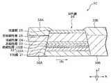
図3は、薄膜磁気ヘッド1の構成を分解して表すものである。また、図4は、図3に示した矢印IV方向から見た平面構造を表し、図5は、図4に示したV−V線に沿った矢視方向の断面構造を表している。また、図6は、図4に示したVI−VI線に沿った矢視方向の断面構造を表している。この薄膜磁気ヘッド1は、磁気媒体3に記録された磁気情報を再生する再生ヘッド部1Aと、磁気媒体3に磁気情報を記録する記録ヘッド部1Bとが一体に構成されたものである。
【0019】
図3および図5に示したように、再生ヘッド部1Aは、基体2Dの上に、絶縁層11,第1シールド層12,第1ギャップ膜13,第2ギャップ膜14,第2シールド層15および絶縁層16がこの順に積層された構造を有している。絶縁層11は、例えば、積層方向の厚さ(以下、単に厚さと記す)が2μm〜10μmであり、Al2O3(酸化アルミニウム)により構成されている。
【0020】
第1シールド層12および第2シールド層15は、例えば、厚さがそれぞれ1μm〜3μmであり、それぞれ3層構造を有している。これら第1シールド層12および第2シールド層15は、MR膜20に不要な磁界の影響が及ばないようにするためのものである。ここで、第1シールド層12および第2シールド層15は、本発明における「第1の磁性層」および「第2の磁性層」の一具体例にそれぞれ対応する。
【0021】
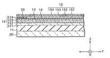
図6に示したように、第1シールド層12および第2シールド層15は、それぞれ第1ギャップ膜13および第2ギャップ膜14を介して、MR膜20を挟み込んでいる。第1シールド層12は、絶縁層11に近い側から、外側層121、下地層122、磁化安定化層123および内側層124を有している。一方、第2シールド層15は、絶縁層11に近い側から、内側層151、磁化安定化層152、隔離層153および外側層154を有している。なお、下地層122および隔離層153は、本発明における「中間層」の一具体例に対応する。
【0022】
第1シールド層12の外側層121は、例えば、厚さが0.5μm〜3.0μmであり、透磁率が高い磁性材料により構成されている。この外側層121は、例えば、Ni(ニッケル)およびFe(鉄)を含む合金により構成されることが好ましい。さらに具体的には、Niの含有率が約80原子%で、Feの含有率が約20原子%であるNiFe(以下、Ni80Fe20と記す。)により構成されることが好ましい。以下の説明では、透磁率が高いこれらの磁性材料を、「高透磁率磁性材料」として説明する。
【0023】
この外側層121は、磁化の向きが自由に変化しうるようになっている(すなわち、磁化の向きが規制されていない)。磁化の向きが自由に変化できれば、不要な磁束が主として外側層121に流れて、MR膜20には流れにくくなり、これにより、MR膜20に不要な磁界が及ぶのを防止する作用(シールド作用)を十分に発揮できるからである。
【0024】
第1シールド層12の下地層122は、厚さが1nm〜30nmであり、例えばTa(タンタル)により構成されている。この下地層122は、その上に成膜される磁化安定化層123の結晶性を向上させるためのものである。また、この下地層122は、外側層121と磁化安定化層123とを隔てることにより、外側層121の磁化の向きが磁化安定化層123によって規制されないようにする機能も有する。
【0025】
第1シールド層12の磁化安定化層123は、例えば、厚さが5nm〜100nmであり、反強磁性材料により構成されている。反強磁性材料としては、例えば、Pt(白金),Ru(ルテニウム),Rh(ロジウム),Pd(パラジウム),Ni,Au(金),Ag(銀),Cu(銅),Ir(イリジウム),Cr(クロム)およびFeからなる群のうちの少なくとも1種と、Mnとを含む反強磁性材料が用いられる。また、Ni,FeおよびCoからなる群のうちの少なくとも1種と、O(酸素)とを含む反強磁性材料を用いてもよい。この磁化安定化層123は、その上に成膜される内側層124との間に交換結合を生じ、これにより、内側層124における磁化の向きをX方向にほぼ固定する(すなわち、規制する)ものである。
【0026】
なお、反強磁性材料には、熱処理しなくても強磁性材料との間に交換結合磁界を誘起する非熱処理系反強磁性材料と、熱処理によって強磁性材料との間に交換結合磁界を誘起する熱処理系反強磁性材料とがある。この磁化安定化層123は、そのどちらにより構成されていてもよい。非熱処理系反強磁性材料にはγ相を有するMn合金などがあり、具体的には、RuRhMn(ルテニウムロジウムマンガン合金),FeMn(鉄マンガン合金)あるいはIrMn(イリジウムマンガン合金)などがある。熱処理系反強磁性材料には規則結晶構造を有するMn合金などがあり、具体的には、PtMn(白金マンガン合金),NiMn(ニッケルマンガン合金)およびPtRhMn(白金ロジウムマンガン合金)などがある。
【0027】
第1シールド層12の内側層124は、例えば、厚さが10nm〜300nmであり、上述した高透磁率磁性材料より構成されている。この第1シールド層12の内側層124は、磁化安定化層123との交換結合により、磁化の向きがX方向にほぼ固定されるようになっている。これは、MR膜20の出力を安定させるためである。
【0028】
第1ギャップ膜13および第2ギャップ膜14は、例えば、厚さがそれぞれ10nm〜100nmであり、Al2O3またはAlN(チッ化アルミニウム)によりそれぞれ構成されている。この第1ギャップ膜13および第2ギャップ膜14は、後述するMR膜20と第1シールド層12および第2シールド層15とを電気的に絶縁するためのものである。絶縁層16は、第1ギャップ膜13および第2ギャップ膜14と同様、例えば厚さが10nm〜100nmであり、Al2O3またはAlNにより構成されている。この絶縁層16は、再生ヘッド部1Aと記録ヘッド部1Bとを電気的に絶縁するためのものである。なお、MR膜20については後述する。
【0029】
第2シールド層15の内側層151は、例えば、厚さが10nm〜300nmであり、上述した高透磁率磁性材料により構成されている。この第2シールド層15の内側層151は、磁化安定化層152との交換結合により、磁化の向きがX方向にほぼ固定されるようになっている。これは、MR膜20の出力を安定させるためである。
【0030】
第2シールド層15の磁化安定化層152は、例えば、厚さが5nm〜100nmであり、第1シールド層12の磁化安定化層123と同様、反強磁性材料により構成されている。反強磁性材料の具体例は、上述したとおりである。この磁化安定化層152は、内側層151との間に交換結合を生じ、これにより内側層151における磁化の向きをX方向にほぼ固定するものである。なお、第1シールド層12の磁化安定化層123および第2シールド層15の磁化安定化層152をいずれも熱処理系反強磁性材料により構成する場合には、磁化安定化層123と内側層124との間に交換結合が生じる温度と、磁化安定化層152と内側層151との間に交換結合が生じる温度とを同じにすることが好ましい。一度の熱処理で、両方の交換結合を生じさせることができるからである。
【0031】
第2シールド層15の隔離層153は、厚さが1nm〜30nmであり、例えばTaにより構成されている。この隔離層153は、磁化安定化層152と外側層154とを隔てることにより、外側層154の磁化の向きが規制されないようにするものである。
【0032】
第2シールド層15の外側層154は、例えば、厚さが0.5μm〜3.0μmであり、上述した高透磁率磁性材料により構成されている。この外側層154は、磁化の向きが自由に変化しうるようになっている。特に、外側層154は、全体に亘って、磁化の向きが自由に変化しうるようになっていることが好ましい。磁化の向きが自由に変化しうるほど、MR膜20に不要な磁界の影響が及ぶのを防止するシールド作用を十分に発揮できるからである。
【0033】
第1ギャップ膜13と第2ギャップ膜14との間には、スピンバルブ膜であるMR膜20を含むMR素子1Cが埋設されている。この再生ヘッド部1Aは、磁気媒体3の信号磁界に応じてMR膜20の電気抵抗が変化することを利用して、磁気媒体3に記録された情報を読み出すようになっている。ここで、MR膜20は、本発明における「機能膜」の一具体例に対応する。
【0034】
図7は、MR素子1Cの断面構造を表す断面図である。このMR素子1CのMR膜20は、第1ギャップ膜13の上に、下地層21,第1軟磁性層22A,第2軟磁性層22B,非磁性層23,強磁性層24,反強磁性層25および保護層26がこの順に積層された構造を有している。下地層21は、例えば、厚さが5nm〜10nmであり、Taにより構成されている。
【0035】
第1軟磁性層22Aは、例えば、厚さが1nm〜3nmであり、Ni,Co(コバルト)およびFeからなる群のうちの少なくともNiを含む磁性材料により構成されている。第2軟磁性層22Bは、例えば、厚さが0.5nm〜3nmであり、Ni,CoおよびFeからなる群のうちの少なくともCoを含む磁性材料により構成されている。この第1軟磁性層22Aおよび第2軟磁性層22Bは、フリー層とも呼ばれる軟磁性層22を構成し、この軟磁性層22では、磁気媒体3からの信号磁界に応じて磁化の向きが変化するようになっている。
【0036】
非磁性層23は、例えば、厚さが1.8nm〜3.0nmであり、Au,Ag,Cu,Ru,Rh,Re(レニウム),PtおよびW(タングステン)からなる群のうち少なくとも1種を含む非磁性材料により構成されている。この非磁性層23は、軟磁性層22を、強磁性層24および反強磁性層25から磁気的にできるだけ隔離するためのものである。
【0037】
強磁性層24は、例えば、厚さが2nm〜4.5nmであり、CoおよびFeからなる群のうちの少なくともCoを含む磁性材料により構成されている。この強磁性層24では、磁性材料の(111)面が積層方向に配向していることが好ましい。なお、この強磁性層24はピンド層とも呼ばれ、反強磁性層25との界面における交換結合により、磁化の向きが固定されている。本実施の形態では、強磁性層24の磁化の向きはY方向に固定されている。
【0038】
反強磁性層25は、例えば、厚さが5nm〜30nmであり、Pt,Ru,Rh,Pd,Ni,Au,Ag,Cu,Ir,CrおよびFeからなる群のうちの少なくとも1種と、Mnとを含む反強磁性材料、または、Ni,FeおよびCoからなる群のうちの少なくとも1種と、Oとを含む反強磁性材料により構成されている。また、この反強磁性層25は、熱処理しなくても強磁性材料との間に交換結合磁界を誘起する非熱処理系反強磁性材料により構成されていてもよいし、熱処理によって強磁性材料との間に交換結合磁界を誘起する熱処理系反強磁性材料により構成されていてもよい。非熱処理系反強磁性材料には、上述したように、RuRhMn,FeMnあるいはIrMnなどがあり、熱処理系反強磁性材料には、PtMn,NiMnおよびPtRhMnなどがある。
【0039】
なお、反強磁性層25を熱処理系反強磁性材料により構成する場合、強磁性層24との交換結合が生じる温度は、第1シールド層12における磁化安定化層123と内側層124との交換結合(および、第2シールド層15における磁化安定化層152と内側層151との交換結合)が生じる温度とは異なることが好ましい。交換結合のための熱処理工程を独立に行うことが可能になるからである。
【0040】
保護層26は、例えば、厚さは5〜10nmであり、Taなどにより構成されている。この保護層26は、薄膜磁気ヘッド1の製造過程においてMR膜20を保護するためのものである。
【0041】
MR膜20の積層方向に対して垂直な方向における両側には、磁区制御膜30A,30Bがそれぞれ設けられている。磁区制御膜30A,30Bは、例えばCoPt(コバルト白金)などの硬磁性材料により形成されており、この磁区制御膜30A,30Bにより、MR膜20に対するバイアス磁界HbがX方向に発生している。磁区制御膜30A,30Bは、このバイアス磁界Hbにより、MR膜20の軟磁性層22の磁化の向きを揃えることにより、いわゆるバルクハウゼンノイズの発生を抑えるようになっている。
【0042】
なお、磁区制御膜30A,30Bを硬磁性材料により形成する代わりに、反強磁性膜と強磁性膜とを積層した構造としてもよい。反強磁性膜としては、上述した熱処理系反強磁性材料および非熱処理系反強磁性材料を用いることができる。反強磁性膜を熱処理系反強磁性材料により構成する場合には、反強磁性膜と強磁性膜との間に交換結合を生じさせるための熱処理が必要であるのに対し、反強磁性膜を非熱処理系反強磁性材料により構成する場合には、熱処理は不要である。
【0043】
これら磁区制御膜30A,30Bの上には、例えばTaよりなるリード層33A,33Bがそれぞれ設けられている。このリード層33A,33Bは、第2ギャップ膜14および絶縁層16に形成された図示しない開口部を介して、端子部33C,33Dに接続されている。これにより、リード層33A,33Bを介してMR膜20に電流をX方向に流すことができるようになっている。
【0044】
記録ヘッド部1Bは、図3および図5に示したように、再生ヘッド部1Aの絶縁層16の上に、NiFeなどの磁性材料よりなる厚さ0.5μm〜3μmの下部磁極41を有している。下部磁極41の上には、Al2O3などの絶縁膜よりなる厚さ0.05μm〜0.3μmの記録ギャップ膜42が形成されている。この記録ギャップ膜42は、後述する薄膜コイル44,46の中心部に対応する位置に開口部42Aを有している。この記録ギャップ膜42の上には、スロートハイトを決定する厚さ1.0μm〜5.0μmのAl2O3などよりなる絶縁層43が形成されており、その絶縁層43の上には、厚さ1μm〜3μmの薄膜コイル44およびこれを覆うフォトレジスト層45がそれぞれ形成されている。このフォトレジスト層45の上には、厚さ1μm〜3μmの薄膜コイル46およびこれを覆うフォトレジスト層47がそれぞれ形成されている。なお、本実施の形態では薄膜コイルが2層積層された例を示したが、薄膜コイルの積層数は1層または3層以上であってもよい。
【0045】
記録ギャップ膜42,絶縁層43およびフォトレジスト層45,47の上には、例えば、NiFeまたはFeN(窒化鉄)などの高飽和磁束密度を有する磁性材料よりなる厚さ約3μmの上部磁極48が形成されている。この上部磁極48は、薄膜コイル44,46の中心部に対応して設けられた記録ギャップ膜42の開口部42Aを介して下部磁極41と接触しており、磁気的に連結している。この上部磁極48の上には、例えば、Al2O3よりなる厚さ20μm〜30μmのオーバーコート層(図15におけるオーバーコート層49)が全体を覆うように形成されている。なお、本実施の形態では、下部磁極41からオーバーコート層までの層構造が記録ヘッド部1Bに対応している。この記録ヘッド部1Bは、薄膜コイル44,46に流れる電流によって下部磁極41と上部磁極48との間に磁束を生じ、記録ギャップ膜42の近傍に生ずる磁束によって磁気媒体3を磁化し、情報を記録するようになっている。
【0046】
<MR素子および薄膜磁気ヘッドの動作>
次に、このように構成された薄膜磁気ヘッド1による再生動作について、図6および図7を中心に参照して説明する。
【0047】
この薄膜磁気ヘッド1では、再生ヘッド部1Aにより、磁気媒体3に記録された情報を読み出す。再生ヘッド部1Aでは、MR膜20の強磁性層24と反強磁性層25との界面での交換結合により、強磁性層24の磁化の向きがY方向に固定されている。また、磁区制御膜30A,30Bの発生するバイアス磁界により、第1軟磁性層22Aおよび第2軟磁性層22Bの磁化はバイアス磁界Hbの方向(ここではX方向)に揃えられる。なお、バイアス磁界Hbと強磁性層24の磁化の向きとは互いにほぼ直交している。情報を読み出す際には、MR膜20に、リード層33A,33Bを通じて定常電流である検出電流(センス電流)が、X方向に流される。
【0048】
このMR膜20では、磁気媒体3の信号磁界に応じて、軟磁性層22における磁化の向きが変化する。一方、強磁性層24の磁化の向きは、反強磁性層25との交換結合により固定されているため、変化しない。軟磁性層22における磁化の向きが変化すると、MR膜20を流れる電流は、軟磁性層22の磁化の向きと強磁性層24の磁化の向きとの相対角度に応じた抵抗を受ける。これは、「スピン依存散乱」と呼ばれる現象によるものである。このMR膜20の抵抗の変化量は電圧の変化量として検出され、磁気媒体3に記録された情報が読み出される。
【0049】
次に、第1シールド層12および第2シールド層15の作用について説明する。磁気媒体3のトラックラインには、図示しない多数のデータ要素(1ビットのデータに対応する領域)がZ方向に一定の間隔で配列されている。MR膜20が、磁気媒体3のあるデータ要素に対向しているときには、そのデータ要素に隣接する他のデータ要素からの磁束は、第1シールド層12および第2シールド層15にそれぞれ流れるため、MR膜20には殆ど流れない。すなわち、第1シールド層12および第2シールド層15は、不要な外部磁界の影響がMR膜20に及ばないようにするシールド作用を発揮する。
【0050】
ここでは、第1シールド層12の外側層121と第2シールド層15の外側層154は、いずれも、磁化の向きが自由に変化しうるようになっているため、読み取り対象でないデータ要素からの磁束は、外側層121および外側層154に流れる。これにより、不要な外部磁界がMR膜20に及ばないようにするシールド作用が十分発揮される。
【0051】
さらに、第1シールド層12の内側層124の磁化の向きは磁化安定化層123によってほぼ固定され、第2シールド層15の内側層151の磁化の向きは磁化安定化層152によってほぼ固定されている。このように、第1シールド層12および第2シールド層15におけるMR膜20に近い側の磁化の向きがほぼ固定されているため、第1シールド層12および第2シールド層15の磁化の向きの変動に起因するMR膜20の抵抗の変動が防止される。すなわち、薄膜磁気ヘッド1の出力が安定する。
【0052】
このように薄膜磁気ヘッド1の出力を安定させ、かつ、シールド作用を十分に発揮させるためには、(1)内側層124および内側層151の磁化の向きが規制されていること、および、(2)外側層121および外側層154の磁化の向きが自由に変化しうることが必要である。これを他の表現で表すと、内側層124および内側層151における一軸異方性磁界よりも、外側層121および外側層154における一軸異方性磁界が0に近いということになる。理想的には、内側層124および内側層151における一軸異方性磁界が0でない値を取り、外側層121および外側層154における一軸異方性磁界が0であることが好ましい。なお、ここで、一軸異方性磁界の値は、対象となっている層の中の平均値であるものとする。
【0053】
<薄膜磁気ヘッドの製造方法>
続いて、図8ないし図15を参照して、MR素子1Cおよび薄膜磁気ヘッド1の製造方法について説明する。なお、図8ないし図15は、図4におけるV−V線に沿った断面構造を表している。
【0054】
本実施の形態に係る製造方法では、まず、図8に示したように、例えば、Al2O3・TiCよりなる基体2Dの一面上に、スパッタリング法により、絶縁層11を構成の欄で述べた材料を用いて成膜する。次に、この絶縁層11の上に、例えば、めっき法により、第1シールド層12の外側層121を、構成の欄で述べた材料を用いて形成する。続いて、この外側層121の上に、例えばスパッタリング法により、下地層122,磁化安定化層123,内側層124を、構成の欄で述べた材料を用いて順次成膜し、第1シールド層12を形成する。そののち、イオンミリング法を用いて、第1シールド層12を図3に示した形状にパターニングする。
【0055】
続いて、この第1シールド層12の上に、例えば、スパッタリング法により、図7に示した下地層21,第1軟磁性層22A,第2軟磁性層22B,非磁性層23,強磁性層24,反強磁性層25および保護層26を、それぞれ構成の欄で説明した材料を用いて順次成膜し、図9に示したMR膜20を形成する。そののち、図10に示したように、MR膜20の上に、パターニング用のフォトレジスト膜51を選択的に形成する。フォトレジスト膜51を形成したのち、例えば、イオンミリング法により、フォトレジスト膜51をマスクとしてエッチングを行うことにより、図7に示した形状のMR膜20が形成される。
【0056】
MR膜20をパターニングしたのち、例えば、スパッタリング法により、MR膜20の両側に、構成の欄で述べた硬磁性材料を用いて、図7に示した磁区制御膜30A,30Bを成膜する。そののち、スパッタリング法により、磁区制御膜30A,30Bの上に、構成の欄で述べた材料を用いて、図7に示したリード層33A,33Bをそれぞれ形成する。そののち、例えば、リフトオフ処理によって、フォトレジスト膜51とその上に積層されている堆積物を除去する。
【0057】
リフトオフ処理を行ったのち、図11に示したように、例えば、スパッタリング法により、第1ギャップ膜13およびMR膜20を覆うように、第2ギャップ膜14を構成の欄で説明した材料を用いて形成する。これにより、MR膜20は第1ギャップ膜13と第2ギャップ膜14との間に埋設される。
【0058】
そののち、第2ギャップ膜14の上に、図12に示したように、例えばスパッタリング法により、第2シールド層15の内側層151,磁化安定化層152,隔離層153、および外側層154の一部を構成の欄で説明した材料を用いて順次成膜する。なお、ここでは、外側層154の最終的な厚さ2μmのうち、例えば30nmだけをスパッタリング法により成膜するものとする。次いで、図13に示したように、外側層154の既に成膜された一部を電極として使用し、めっき法により、外側層154の残りの部分(厚さ約2μm)を形成することにより、第2シールド層15を形成する。そののち、イオンミリング法を用いて、第2シールド層15を図3に示した形状にパターニングする。
【0059】
第2シールド層15をパターニングしたのち、図14に示したように、例えばスパッタリング法により、絶縁層16を構成の欄で説明した材料を用いて成膜する。絶縁層16を形成したのち、絶縁層16の上に、例えばスパッタリング法により、下部磁極41を構成の欄で説明した材料を用いて成膜する。次いで、下部磁極41の上に、例えばスパッタリング法により、記録ギャップ膜42を形成し、その上に、絶縁層43を所定のパターンに形成する。絶縁層43を形成したのち、この絶縁層43の上に、薄膜コイル44を構成の欄で説明した材料を用いて形成し、この薄膜コイル44を覆うようにフォトレジスト層45を所定のパターンに形成する。フォトレジスト層45を形成したのち、このフォトレジスト層45の上に、薄膜コイル46を構成の欄で説明した材料を用いて形成し、この薄膜コイル46を覆うようにフォトレジスト層47を所定のパターンに形成する。
【0060】
フォトレジスト層47を形成したのち、図15に示したように、例えば、薄膜コイル44,46の中心部に対応する位置において、記録ギャップ膜42を部分的にエッチングし、磁路形成のための開口部42Aを形成する。そののち、例えば、記録ギャップ膜42、開口部42A,絶縁層43およびフォトレジスト層45,47の上に上部磁極48を構成の欄で説明した材料を用いて形成する。上部磁極48を形成したのち、例えば、この上部磁極48をマスクとして、イオンミリングにより、記録ギャップ膜42および下部磁極41を選択的にエッチングする。そののち、上部磁極48の上に、オーバーコート層49を構成の欄で説明した材料を用いて形成する。
【0061】
続いて、交換結合を生じさせるための熱処理を行う。ここでは、MR膜20の強磁性層24と反強磁性層25との交換結合を起こさせる第1の熱処理と、第1シールド層12における内側層124と磁化安定化層123との交換結合および第2シールド層15における内側層151と磁化安定化層152との交換結合を起こさせる第2の熱処理を行う。
【0062】
ここでは、MR膜20の強磁性層24と反強磁性層25との交換結合を起こさせる第1の熱処理温度を例えば250℃とする。また、第1のシールド層12における内側層124と磁化安定化層123との交換結合を起こさせる温度と、第2のシールド層15における内側層151と磁化安定化層152との交換結合とを起こさせる温度とは等しく(第2の熱処理温度とする。)、例えば200℃とする。
【0063】
この場合、まず、MR膜20の反強磁性層25と強磁性層24との間に交換結合を生じさせるため、磁界発生装置などを利用して例えばY方向に磁界を印加しつつ、第1の熱処理温度に加熱する。これにより、MR膜20の強磁性層24の磁化の向きは、反強磁性層25との交換結合によって印加磁界の方向Yに固定される。そののち、温度を第2の熱処理温度まで低下させ、磁界発生装置により印加する磁界の方向をX方向に変えて、第1のシールド層12における内側層124と磁化安定化層123との交換結合、および、第2のシールド層15における内側層151と磁化安定化層152との交換結合を生じさせる第2の熱処理を行う。
【0064】
なお、第1の熱処理温度が第2の熱処理温度よりも低いも場合には、まず第2の熱処理を行い、そののち、温度を降下させ、磁界の印加方向を変えて第1の熱処理と行う。
【0065】
最後に、例えば、スライダ2のエアベアリング面2Eを研磨加工し、薄膜磁気ヘッド1が完成する。
【0066】
<実施の形態による効果>
以上説明したように、本実施の形態によれば、第1シールド層12および第2シールド層15においてMR膜20側に位置する内側層124および内側層151の磁化の向きを、磁化安定化層123および磁化安定化層152によって規制するようにしたので、第1シールド層12および第2シールド層15の磁化の向きの変動に起因したMR膜20の抵抗の変動を防止することができる。すなわち、薄膜磁気ヘッド1の出力を安定させることができる。
【0067】
さらに、第1シールド層12の外側層121および第2シールド層15の外側層154の磁化の向きを規制せず、自由に変化できるようにしたので、外部磁界の影響がMR膜20に及ばないようにするシールド作用を十分に発揮することができる。すなわち、第1シールド層12および第2のシールド層15の本来の機能を十分発揮しつつ、薄膜磁気ヘッド1の出力を安定させることができる。
【0068】
加えて、第1シールド層12の内側層124および第2シールド層15の内側層151の磁化の向きの規制を、反強磁性を有する磁化安定化層123および磁化安定化層152との交換結合を利用して行うようにしたので、磁化の向きの規制を比較的簡単な方法で行うことができる。
【0069】
また、第1シールド層12において、下地層122,磁化安定化層123および内側層124の3層と、外側層121とを、別々の成膜方法を用いて、非連続なプロセスにより形成するようにしたので、内側層124の磁化の向きを規制するための熱処理の際に、外側層121の磁化の向きまでが規制されてしまうことが抑制される。
【0070】
さらに、第1シールド層12の外側層121と磁化安定化層123との間に下地層122を介在させ、第2シールド層15の外側層154と磁化安定化層152との間に隔離層153を介在させるようにしたので、外側層121および外側層154の磁化の向きが規制されてしまうことが防止される。
【0071】
また、MR膜20の強磁性層24と反強磁性層25との交換結合を起こさせる第1の熱処理温度と、第1シールド層12の内側層124と磁化安定化層123との交換結合(および、第2シールド層15の内側層151と磁化安定化層152との交換結合)を起こさせる第2の熱処理温度とが異なるようにしたので、強磁性層24の磁化の向きを規制するための熱処理と、内側層124および内側層151の磁化の向きを規制するための熱処理とを、独立して行うようにすることができる。
【0072】
加えて、内側層124および内側層151の磁化の向きが、磁区制御膜30A,30BによってMR膜20に印加されるバイアス磁界Hbとほぼ平行(同じ向き、反対向きの両方を含む)になるようにしたので、外側層121および外側層154における磁界がMR膜20に与える影響を低減させることができる。
【0073】
<第1の変形例>
次に、本実施の形態における第1の変形例について説明する。本変形例における薄膜磁気ヘッド101は、上記の実施の形態で説明した薄膜磁気ヘッド1に対し、第2シールド層の構造のみが異なるものである。なお、ここでは、図1ないし図15に示した第1の実施の形態における構成要素と同一の部分には同一の符号を付し、適宜説明を省略する。
【0074】
図16は、本変形例における薄膜磁気ヘッド101の再生ヘッド部を磁気媒体側から見た図であり、図4におけるVI−VI断面に対応するものである。本変形例では、第2シールド層150は、単層構造を有しており、上述した高透磁率磁性材料により構成されている。第2シールド層150の厚さは、例えば1μm〜3μmである。すなわち、この第2シールド層150は、その全体に亘って、磁化の向きが自由に変化しうるようになっている。
【0075】
本変形例では、第1シールド層12においてMR膜20に近い側の磁化の向きは規制されているが、第2シールド層150では磁化の向きは全く規制されていないため、MR素子1Cの出力変動を抑制する効果は、上記の第1の実施の形態よりも僅かに低下する。しかしながら、第2シールド層150の磁化の向きが全体的に自由に変化しうるため、不要な磁束が第2シールド層150に流れ易くなり、これにより、不要な磁界がMR膜20に及ばないようにするシールド作用が向上する。
【0076】
<第2の変形例>
次に、本実施の形態における第2の変形例について説明する。本変形例における薄膜磁気ヘッド102は、上記の実施の形態で説明した薄膜磁気ヘッド1に対し、第1シールド層の構造のみが異なるものである。なお、ここでは、図1ないし図15に示した第1の実施の形態における構成要素と同一の部分には同一の符号を付し、適宜説明を省略する。
【0077】
図17は、本変形例における薄膜磁気ヘッド102の再生ヘッド部を磁気媒体側から見た図であり、図4におけるVI−VI断面に対応するものである。図17に示したように、本変形例では、第1シールド層120は、単層構造を有しており、上述した高透磁率磁性材料により構成されている。この第1シールド層120の厚さは、例えば1μm〜3μmである。すなわち、この第1シールド層120は、その全体に亘って、磁化の向きが自由に変化しうるようになっている。
【0078】
本変形例では、第2シールド層15においてMR膜20に近い側の磁化の向きは規制されているが、第1シールド層120では磁化の向きは全く規制されていないため、MR素子1Cの出力変動を抑制する効果は、上記の第1の実施の形態よりも僅かに低下する。しかしながら、第1シールド層120の磁化の向きが全体的に自由に変化しうるため、不要な磁束が第1シールド層120に流れ易くなり、これにより、不要な磁界がMR膜20に及ばないようにするシールド作用が向上する。
【0079】
[第2の実施の形態]
次に、本実施の形態における第2の実施の形態について説明する。本実施の形態における薄膜磁気ヘッド103は、上記第1の実施の形態で説明した薄膜磁気ヘッド1における磁化安定化層を、反強磁性材料の代わりに硬磁性材料により形成するようにしたものである。
【0080】
図18は、本実施の形態における薄膜磁気ヘッド103の再生ヘッド部を磁気媒体側から見た図であり、図4におけるVI−VI断面に対応するものである。ここでは、図1ないし図15に示した第1の実施の形態における構成要素と同一の部分には同一の符号を付し、適宜説明を省略する。
【0081】
本実施の形態における第1シールド層220は、絶縁層11側から、外側層121,補助層222,磁化安定化層223および内側層124とを有している。外側層121および内側層124は、いずれも第1の実施の形態と同様に構成されている。
【0082】
磁化安定化層223は、例えば、厚さ15〜100nmであり、硬磁性材料により構成されている。ここで、硬磁性材料とは、具体的には、CoPt(コバルト白金合金)、CoPtCr(コバルト白金クロム合金)、NdFeB(ネオジウム鉄ホウ素合金)、SmCu(アンチモン銅合金)などである。補助層222は、例えば、1〜10nmであり、例えばCrにより構成されている。この補助層222は、磁化安定化層223の永久磁石としての特性を発揮させるためのものである。
【0083】
第1シールド層220の磁化安定化層223は、その磁化の向きがX方向にほぼ固定されている。この磁化安定化層223の磁化の影響は、その磁化安定化層223に隣接する内側層124に及ぶため、内側層124の磁化の向きはX方向にほぼ固定される。すなわち、第1シールド層220の磁化安定化層223は、内側層124の磁化の向きをX方向にほぼ固定する機能を有している。なお、外側層121と磁化安定化層223との間には補助層222が介在しているため、外側層121の磁化の向きが固定されることはない。すなわち、第1シールド層220の外側層121では、磁化の向きが自由に変化する。
【0084】
また、本実施の形態における第2シールド層250は、絶縁層11側から、内側層151,補助層252,磁化安定化層253,隔離層253Aおよび外側層154とを有している。内側層151および外側層154は、いずれも第1の実施の形態と同様に構成されている。
【0085】
第2シールド層250の磁化安定化層253は、上述した硬磁性材料により構成されており、その厚さは、例えば15〜100nmである。補助層252は、例えば、厚さ1〜10nmであり、例えばCrにより構成されている。この補助層252は、磁化安定化層253の永久磁石としての特性を発揮させるためのものである。隔離層253Aは、例えばTaにより構成され、その厚さは、例えば1〜10nmである。この隔離層253Aは、磁化安定化層253の磁化により外側層154の磁化の向きが固定されないようにするためのものである。
【0086】
第2シールド層250の磁化安定化層253は、その磁化の向きがX方向にほぼ固定されている。この磁化安定化層253の磁化の影響は、その磁化安定化層253に(補助層252を隔てて)隣接する内側層151に及び、この内側層151の磁化はX方向にほぼ固定される。すなわち、第2シールド層250の磁化安定化層253は、内側層151の磁化の向きをX方向にほぼ固定する機能を有している。なお、外側層154と磁化安定化層253とは、隔離層253Aによって隔離されているため、磁化安定化層253の磁化の影響は外側層154には殆ど及ばない。すなわち、第2シールド層250の外側層154では、磁化の向きが自由に変化する。
【0087】
本実施の形態では、磁化安定化層223および磁化安定化層253の作用により、第1シールド層220の内側層124および第2シールド層250の内側層151の磁化の向きがX方向にほぼ固定される。従って、第1の実施の形態と同様、第1シールド層220および第2シールド層250における磁化の向きの変動によってMR膜20の抵抗が変動することが防止される。すなわち、薄膜磁気ヘッド103の安定した出力が得られる。
【0088】
また、第1シールド層220および第2シールド層250において、外側層121および外側層154では、磁化の向きが自由に変化しうるので、第1の実施の形態と同様、十分なシールド作用が発揮される。
【0089】
<第1の変形例>
次に、本実施の形態における第1の変形例について説明する。本変形例における薄膜磁気ヘッド104は、上記第2の実施の形態で説明した薄膜磁気ヘッドに対し、第2シールド層の構造のみが異なるものである。なお、ここでは、図18に示した第2の実施の形態における構成要素と同一の部分には同一の符号を付し、適宜説明を省略する。
【0090】
図19は、本変形例における薄膜磁気ヘッド104の再生ヘッド部を磁気媒体側から見た図であり、図4におけるVI−VI断面に対応するものである。本変形例では、第2シールド層150は、単層構造を有しており、上述した高透磁率磁性材料により構成されている。第2シールド層150の厚さは、例えば1μm〜3μmである。すなわち、この第2シールド層150は、その全体に亘って、磁化の向きが自由に変化しうるようになっている。
【0091】
本変形例では、第1シールド層220においてMR膜20に近い側の磁化の向きは規制されているが、第2シールド層150では磁化の向きは全く規制されていないため、MR素子1Cの出力変動を抑制する効果は、上記の第2の実施の形態よりも僅かに低下する。しかしながら、第2シールド層150の磁化の向きが全体的に自由に変化しうるため、不要な磁束が第2シールド層150に流れ易くなり、これにより、不要な磁界がMR膜に及ばないようにするシールド作用が向上する。
【0092】
<第2の変形例>
次に、本実施の形態における第2の変形例について説明する。本変形例における薄膜磁気ヘッド105は、上記第2の実施の形態で説明した薄膜磁気ヘッドに対し、第1シールド層の構造のみが異なるものである。なお、ここでは、なお、ここでは、図18に示した第2の実施の形態における構成要素と同一の部分には同一の符号を付し、適宜説明を省略する。
【0093】
図20は、本変形例における薄膜磁気ヘッド105の再生ヘッド部を磁気媒体側から見た図であり、図4におけるVI−VI断面に対応するものである。図20に示したように、本変形例では、第1シールド層120は、単層構造を有しており、上述した高透磁率磁性材料により構成されている。この第1シールド層120の厚さは、例えば1μm〜3μmである。すなわち、この第1シールド層120は、その全体に亘って、磁化の向きが自由に変化しうるようになっている。
【0094】
本変形例では、第2シールド層250においてMR膜20に近い側の磁化の向きは規制されているが、第1シールド層120では磁化の向きは全く規制されていないため、MR素子1Cの出力変動を抑制する効果は、上記の第2の実施の形態よりも僅かに低下する。しかしながら、第1シールド層120の磁化の向きが全体的に自由に変化しうるため、不要な磁界を第1シールド層120に取り込み易くなり、これにより、不要な磁界がMR膜に及ばないようにするシールド作用が向上する。
【実施例】
次に、本発明の具体的な実施例について詳細に説明する。
【0095】
[実施例1]
実施例1として、図6に示した薄膜磁気ヘッド1を作成した。まず、Al2O3・TiC製の基体2Dの上に、スパッタリング法により、Al2O3を用いて厚さ2μmの絶縁層11を成膜し、その上に、めっき法により、Ni80Fe20を用いて厚さ2μmの外側層121を形成した。そののち、スパッタリング法により、外側層121の上に、Taを用いて厚さ5nmの下地層122を成膜し、その上に、RuMnを用いて厚さ20nmの磁化安定化層123を成膜し、さらに、その磁化安定化層123の上に、例えばNiFeを用いて厚さ30nmの内側層124を成膜した。
【0096】
次いで、第1シールド層12の内側層124の上に、スパッタリング法により、Al2O3を用いて厚さ10nmの第1ギャップ膜13を成膜した。続いて、スパッタリング法により、第1ギャップ膜13の上に、Taを用いて厚さ5nmの下地層21を成膜し、その上に、Ni80Fe20を用いて厚さ3nmの第1軟磁性層22Aを成膜し、その上に、CoFeを用いて厚さ1nmの第2軟磁性層22Bを成膜した。続いて、スパッタリング法により、第2軟磁性層22Bの上に、Cuを用いて厚さ2.5nmの非磁性層23を成膜し、その上に、CoFeを用いて厚さ2nmの強磁性層24を成膜し、その上に、PtMnを用いて厚さ20nmの反強磁性層25を成膜し、その上に、Taを用いて厚さ5nmの保護層26を成膜した。
【0097】
次いで、下地層21から保護層26までの積層膜を、イオンミリングによりパターニングして、図7に示した形状のMR膜20を形成し、そのMR膜20の両側に、スパッタリング法により、CoPtを用いて厚さ50nmの磁区制御膜30A,30Bを成膜し、その上に、スパッタリング法により、厚さ100nmのリード層33A,33Bを所定の形状に形成した。
【0098】
リード層33A,33Bを形成したのち、MR膜20,磁区制御膜30A,30Bおよびリード層33A,33Bを覆うように、スパッタリング法により、Al2O3を用いて厚さ10nmの第2ギャップ膜14を成膜した。次いで、スパッタリング法により、第2ギャップ膜14の上に、Ni80Fe20を用いて厚さ30nmの内側層151を成膜し、その内側層151の上に、RuMnを用いて厚さ20nmの磁化安定化層152を成膜し、その磁化安定化層152の上に、Taを用いて厚さ5nmの隔離層153を成膜し、さらに、その隔離層153の上に、Ni80Fe20を用いて外側層154の一部を厚さ30nmだけ成膜した。次いで、この外側層154の一部(厚さ30nmの部分)を電極膜として、めっき法により、Ni80Fe20を用いて厚さ2μmの外側層154を形成した。
【0099】
第2シールド層15の上には、図5に示した絶縁層16,下部磁極41,記録ギャップ膜42,絶縁層43,薄膜コイル44,フォトレジスト層45,薄膜コイル46,フォトレジスト層47,上部磁極48およびオーバーコート層49を積層した。絶縁層16からオーバーコート層49までの部分(記録ヘッド部1B)は、本実施例における測定事項に影響を与えないため、詳細説明は省略する。
【0100】
次いで、MR膜20の反強磁性層25と強磁性層24との間に交換結合を生じさせるため、磁界発生装置を利用して例えばY方向に磁界を印加しつつ、250℃に加熱した。そののち、温度を200℃まで低下させ、磁界発生装置により印加する磁界の方向をX方向に変えて、第1のシールド層12における内側層124と磁化安定化層123との交換結合、および、第2のシールド層15における内側層151と磁化安定化層152との交換結合を生じさせた。
【0101】
[実施例2]
実施例2として、図16に示した薄膜磁気ヘッド101を作製した。製造方法は、第2シールド層の製造工程において、第2ギャップ膜14の上に、めっき法によりNi80Fe20を用いて厚さ2μmの第2シールド層150を形成したことを除き、実施例1と同じである。
【0102】
[実施例3]
実施例3として、図17に示した薄膜磁気ヘッド102を作製した。製造方法は、第1シールド層の製造工程において、絶縁層11の上に、めっき法によりNi80Fe20を用いて厚さ2μmの第1シールド層120を形成したことを除き、実施例1と同じである。
【0103】
[実施例4]
実施例4として、図18に示した薄膜磁気ヘッド103を作製した。まず、Al2O3・TiC製の基体2Dの上に、スパッタリング法により、Al2O3を用いて厚さ2μmの絶縁層11を成膜し、その上に、めっき法により、Ni80Fe20を用いて厚さ2μmの外側層121を形成した。そののち、スパッタリング法により、外側層121の上に、Crを用いて厚さ5nmの補助層222を成膜し、その補助層222の上に、CoPtを用いて厚さ20nmの磁化安定化層223を成膜し、さらに、その磁化安定化層223の上に、例えばNi80Fe20を用いて厚さ30nmの内側層124を成膜した。
【0104】
次いで、第1シールド層220の内側層124の上に、実施例1と同様に、第1ギャップ膜13、下地層21、第1軟磁性層22A、第2軟磁性層22B、非磁性層23、強磁性層24、反強磁性層25および保護層26を順次成膜し、MR膜20を形成した。さらに、実施例1と同様に、MR膜20を挟み込むように、磁区制御膜30A,30Bおよびリード層33A,33Bを形成した。次いで、実施例1と同様に、第2ギャップ膜14を成膜した。
【0105】
次いで、スパッタリング法により、第2ギャップ膜14の上に、Ni80Fe20を用いて厚さ30nmの内側層151を成膜し、その内側層151の上に、Crを用いて厚さ10nmの補助層252を成膜し、その補助層252の上に、CoPtを用いて厚さ20nmの磁化安定化層253を成膜した。次いで、スパッタリング法により、磁化安定化層253の上に、Taを用いて厚さ5nmの隔離層253Aを成膜し、その隔離層253Aの上に、Ni80Fe20を用いて外側層154の一部を厚さ30nmだけ成膜した。次いで、この外側層154における厚さ30nmの部分を電極膜として利用して、めっき法により、Ni80Fe20を用いて厚さ2μmの外側層154を形成した。
【0106】
第2シールド層250の上には、実施例1と同様に、絶縁層16,下部磁極41,記録ギャップ膜42,絶縁層43,薄膜コイル44,フォトレジスト層45,薄膜コイル46,フォトレジスト層47,上部磁極48およびオーバーコート層49を積層した。次いで、MR膜20の反強磁性層25と強磁性層24との間に交換結合を生じさせるため、磁界発生装置を利用して例えばY方向に磁界を印加しつつ、250℃に加熱した。
【0107】
[実施例5]
実施例5として、図19に示した薄膜磁気ヘッド104を作製した。製造方法は、第2シールド層の製造工程において、第2ギャップ膜14の上に、めっき法によりNi80Fe20を用いて厚さ2μmの第2シールド層150を形成したことを除き、実施例4と同じである。
【0108】
[実施例6]
実施例6として、図20に示した薄膜磁気ヘッド105を作製した。製造方法は、第1シールド層の製造工程において、絶縁層11の上に、めっき法によりNi80Fe20を用いて厚さ2μmの第1シールド層120を形成したことを除き、実施例4と同じである。
【0109】
このように作製した薄膜磁気ヘッドのそれぞれについて、出力変動値(COV;Covariant)を測定した。その結果を、表1に示す。ここで、出力変動値は、各薄膜磁気ヘッドに繰り返し信号磁界を与えてヘッド出力を測定し、ヘッド出力のばらつきの標準偏差σ(シグマ)をヘッド出力の平均値で割ったものである。
【0110】
【表1】
[比較例]
また、本実施例に対する比較例として、第1シールド層12および第2シールド層15を、いずれも単層構造とし、Ni80Fe20を用いてそれぞれ厚さ2μmに形成した薄膜磁気ヘッドを作成した。この薄膜磁気ヘッドについても、出力の変動率を測定した。その結果を表1に合わせて示す。
【0112】
表1から分かるように、実施例1ないし実施例6では、出力変動値が0.5%〜2.0%となり、比較例(10%)よりも良好な値が得られた。特に、第1シールド層と第2シールド層の両方に磁化安定化層を設けた実施例1および実施例4では、出力変動値が0.5%と最も良好な値が得られた。このことから、第1シールド層および第2シールド層の少なくとも1方に磁化安定化層を設けると、出力が安定し、さらに、第1シールド層および第2シールド層の両方に磁化安定化層を設けると、出力が最も安定することが分かった。さらに、実施例1〜3と実施例4〜6とをそれぞれ比較すると、磁化安定化層を反強磁性材料により構成した場合でも、硬磁性材料により構成した場合でも、同等の効果が得られることが分かった。
【0113】
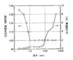
次に、実施例1の薄膜磁気ヘッドにおいて、第1シールド層12の内側層124と第2シールド層15の内側層151の厚さを2nm〜500nmまで変化させ、それぞれ、出力変動値(COV;Covariant)および出力波形の半値幅を測定した。その結果を、図21に示す。ここで、出力波形の半値幅は、各薄膜磁気ヘッドに繰り返し信号磁界を与えてヘッド出力を測定したときの、信号波形の半値幅の平均値から求めたものである。この出力波形の半値幅は、再生ヘッド部の分解能に対応するものである。
【0114】
図21から、内側層124および内側層151の厚さが10nm以上の場合には、出力波形の半値幅はほぼ一定であり、内側層124および内側層151の厚さが10nm未満になると出力波形の半値幅が増加することが分かる。これは、内側層124および内側層151の厚さが薄すぎると、内側層124および内側層151の磁化の向きが完全に固定されてしまい、内側層124および内側層151において磁化の向きが変化する余地が全く無くなることから、第1シールド層12および第2シールド層15のシールド作用が僅かに低下するためである。
【0115】
さらに、内側層124および内側層151の厚さが300nm以下の場合には、出力変動値が、許容限界である5%以下に収まっているが、厚さが300nmを超えると、出力変動値が5%を超えている。これは、内側層124および内側層151の厚さが厚すぎると、交換結合が内側層124および内側層151におけるMR膜20近傍領域までそれぞれ十分には及ばなくなることから、MR膜20の近傍の領域において磁化の向きが変動するようになるためである。
【0116】
すなわち、図21から、第1シールド層12の内側層124の厚さ、および、第2シールド層15の内側層151の厚さが、それぞれ、10nm以上300nm以下であれば、特に良好な出力変動値を得ると共に、出力は系の半値幅を狭くして分解能を向上できることが分かる。
【0117】
図22は、第1シールド層12の内側層124と第2シールド層15の内側層151の厚さを2nm〜500nmまで変化させた場合の、内側層124および内側層151における一軸異方性磁界(Hua)を測定した結果を表す特性図である。
【0118】
図22に示したように、内側層124および内側層151の厚さが薄いほど一軸異方性磁界が大きくなることが分かる。また、内側層124および内側層151の厚さが厚いほど一軸異方性磁界が小さくなり、内側層124および内側層151の厚さが500nm以上になるとほぼ0になることが分かる。これは、内側層124および内側層151の厚さが薄いほど、磁化の向きが強く規制され、内側層124および内側層151が厚いほど、磁化の向きが変化する余地が生まれるためである。
【0119】
図21に示した内側層124および内側層151の好ましい厚さ(10nm〜300nm)に対応する一軸異方性磁界は、約480A/m(6Oe)〜15900A/m(20Oe)である。すなわち、内側層124および内側層151における一軸異方性磁界が、480A/m〜15900A/mの範囲にあれば、出力変動を好ましい範囲に抑制しつつ、高密度記録に対応することができることが分かった。
【0120】
以上、実施の形態および実施例を挙げて本発明を説明したが、本発明はこの実施の形態および実施例に限定されるものではなく、種々の変形が可能である。例えば、第1シールド層の磁化安定化層を反強磁性材料とし、第2シールド層の磁化安定化層を硬磁性材料としてもよいし、第1シールド層の磁化安定化層を硬磁性材料とし、第2シールド層の磁化安定化層を反強磁性材料としてもよい。
【0121】
加えて、磁化安定化層を、第1シールド層または第2シールド層において、MR膜に対応する局所的な領域のみに形成するようにしてもよい。
【0122】
また、上述した実施の形態においては、MR膜20の反強磁性層25を熱処理系反強磁性材料により構成したが、非熱処理系反強磁性材料により構成してもよい。この場合には、熱処理を行わなくとも、反強磁性層25と強磁性層24との界面で交換結合を誘起させることができる。
【0123】
また、上記の実施の形態では、磁区制御膜30A,30Bを硬磁性材料により形成したが、反強磁性膜と強磁性膜とを積層した構造としてもよい。反強磁性膜を熱処理系反強磁性材料により構成する場合には、反強磁性膜と強磁性膜との間に交換結合を生じさせるための熱処理が必要である。反強磁性膜を非熱処理系反強磁性材料により構成する場合には、熱処理は不要である。
【0124】
さらに、薄膜磁気ヘッド1のMR膜は、スピンバルブ膜には限定されず、他の種類のGMR膜、AMR膜、またはTMR(Tunnel-type Magneto-Resistive )膜などであっても良い。また、薄膜磁気ヘッド1は、再生専用ヘッドであっても良く、磁気センサやメモリであってもよい。
【0125】
【発明の効果】
以上説明したように、請求項1ないし請求項8のいずれか1項に記載の薄膜磁気ヘッドまたは請求項9ないし請求項12のいずれか1項に記載の薄膜磁気ヘッドの製造方法によれば、第1のシールド層および第2のシールド層の少なくとも一方が、機能膜側から順に、磁化の向きが規制された内側層と、内側層の磁化の向きを規制する磁化安定化層と、磁化の向きが変化しうる外側層とを有するようにしたので、第1のシールド層および第2のシールド層の少なくとも一方における機能膜に近い側の磁化の向きの変動が抑制され、薄膜磁気ヘッドの安定した出力を得ることができる。また、外側層により不要な磁界を取り込むことができるため、高密度化に伴って第1シールド層と第2シールド層との間隔を狭くした場合でも、機能膜に不要な磁界が及ぶことが防止される。すなわち、高密度記録に対応しつつ、薄膜磁気ヘッドの出力を安定させることができる。
【0126】
特に、請求項2記載の薄膜磁気ヘッドによれば、内側層の厚さを10nm以上300nmとしたので、薄膜磁気ヘッドの出力を安定させ、かつ、高密度記録に対応できる分解能を得ることができる。
【0127】
さらに、請求項3記載の薄膜磁気ヘッドによれば 磁化安定化層が反強磁性材料または硬磁性材料を含むようにしたので、内側層の磁化の向きを容易に規制することができる。
【0128】
また、請求項4記載の薄膜磁気ヘッドによれば、磁化安定化層と外側層との間に中間層を設けるようにしたので、内側層の磁化の向きのみを規制して、外側層の磁化の向きが自由に変化できるようにすることができる。
【0129】
加えて、請求項5記載の薄膜磁気ヘッドによれば、内側層の磁化の向きを、磁区制御膜が機能膜に印加するバイアス磁界の向きに対してほぼ平行になるようにしたので、シールド層における磁界が機能膜に及ぼす影響を低減することができる。
【0130】
さらに、請求項6記載の薄膜磁気ヘッドによれば、機能膜における反強磁性層と強磁性層との交換結合が生じる第1の温度と、磁化安定化層と内側層との交換結合が生じる第2の温度とが異なるようにしたので、強磁性層の磁化および内側層の磁化を、それぞれ独立に規制することが可能になる。
【0131】
また、請求項8記載の薄膜磁気ヘッドによれば、内側層における一軸異方性磁界よりも、外側層における一軸異方性磁界の方が0に近くなるようにしたので、内側層では磁化の向きが変動しにくく、外側層では磁化の向きが変化しやすくなる。すなわち、高密度記録に対応しつつ、薄膜磁気ヘッドの出力を安定させることができる。
【0132】
また、請求項11記載の薄膜磁気ヘッドの製造方法によれば、内側層と磁化安定化層とをほぼ同一の成膜方法を用いて連続的に成膜するようにしたので、磁化安定化層が反強磁性材料よりなる場合には、内側層と磁化安定化層との間で交換結合を生じさせ易くなる。
【0133】
さらに、請求項12記載の薄膜磁気ヘッドの製造方法によれば、磁化安定化層と外側層とを、非連続的に成膜するようにしたので、磁化安定化層が反強磁性材料よりなる場合には、外側層と磁化安定化層との間に交換結合を生じさせないようにすることができる。
【図面の簡単な説明】
【図1】本発明の一実施の形態に係る薄膜磁気ヘッドを搭載した回転アームの外形形状を表す斜視図である。
【図2】本発明の一実施の形態に係る薄膜磁気ヘッドが形成されたスライダの外形形状を表す斜視図である。
【図3】本発明の一実施の形態に係る薄膜磁気ヘッドの構造を分解して表す分解斜視図である。
【図4】図3に示した薄膜磁気ヘッドの平面形状を表す平面図である。
【図5】図3に示した薄膜磁気ヘッドのエアベアリング面に直交する面における断面構造を表す断面図である。
【図6】図3に示した薄膜磁気ヘッドのエアベアリング面と平行な面における断面構造を表す断面図である。
【図7】図3に示した薄膜磁気ヘッドのMR素子の構造を拡大して示す断面図である。
【図8】図3に示した薄膜磁気ヘッドの製造方法における一工程を説明するための断面図である。
【図9】図8に続く工程を説明するための断面図である。
【図10】図9に続く工程を説明するための断面図である。
【図11】図10に続く工程を説明するための断面図である。
【図12】図11に続く工程を説明するための断面図である。
【図13】図12に続く工程を説明するための断面図である。
【図14】図13に続く工程を説明するための断面図である。
【図15】図14に続く工程を説明するための断面図である。
【図16】第1の実施の形態の第1の変形例に係る薄膜磁気ヘッドの断面構造を表す断面図である。
【図17】第1の実施の形態の第2の変形例に係る薄膜磁気ヘッドの断面構造を表す断面図である。
【図18】本実施の形態の第2の実施の形態に係る薄膜磁気ヘッドの断面構造を表す断面図である。
【図19】第2の実施の形態の第1の変形例に係る薄膜磁気ヘッドの断面構造を表す断面図である。
【図20】第2の実施の形態の第2の変形例に係る薄膜磁気ヘッドの断面構造を表す断面図である。
【図21】本発明の実施例における出力変動値および分解能の測定定結果を表す特性図である。
【図22】本発明の実施例における一軸異方性磁界の測定結果を表す特性図である。
【符号の説明】
1…薄膜磁気ヘッド、1A…再生ヘッド部、1B…記録ヘッド部1B、2…スライダ、2D…基体、11…絶縁層、12…第1シールド層、121…外側層、122…下地層、123…磁化安定化層、124…内側層、13…第1ギャップ膜、14…第2ギャップ膜、15…第2シールド層、151…内側層、152…補助層、153…磁化安定化層、153A…隔離層、154…外側層、16…絶縁層、20…MR膜、21…下地層、22…軟磁性層、22A…第1軟磁性層、22B…第2軟磁性層、23…非磁性層、24…強磁性層、25…反強磁性層、26…保護層、30A,30B…磁区制御膜、33A,33B…リード層。[0001]
BACKGROUND OF THE INVENTION
The present invention relates to a thin film magnetic head used in a magnetic recording device such as a hard disk device and a method for manufacturing the same.
[0002]
[Prior art]
In recent years, with improvement in surface recording density of hard disks and the like, improvement in performance of thin film magnetic heads has been demanded. As the thin film magnetic head, a composite thin film magnetic head having a structure in which a reproducing head having a magnetoresistive element (hereinafter referred to as an MR (Magnetoresistive) element) and a recording head having an inductive magnetic transducer is laminated is widely used. It is used. The MR element has a single-layer or multi-layer magnetoresistive film (hereinafter referred to as an MR film) that exhibits a resistance change in response to a signal magnetic field, and information is read based on the resistance change in the MR film. To do. Known MR films include an AMR film exhibiting an anisotropic magnetoresistive effect (AMR (Anisotropic Magnetoresistive) effect) and a GMR film exhibiting a giant magnetoresistive effect (GMR (Giant Magnetoresistive) effect).
[0003]
Here, the magnetic medium has a track line in which a large number of data elements (area corresponding to 1-bit information) are arranged, and the interval between the data elements is extremely short. Therefore, it is necessary that the MR film of the thin film magnetic head is not affected by other adjacent data elements when reading information of a certain data element. Therefore, in the thin film magnetic head, the MR film is sandwiched between a pair of shield layers made of a magnetic material having a high magnetic permeability. That is, unnecessary magnetic flux (that is, magnetic flux from an adjacent data element) flows mainly to the shield layer and does not flow to the MR film, so that an unnecessary magnetic field does not reach the MR film. Such an action is called a shield action. The distance between the pair of shield layers substantially corresponds to the distance between the data elements in the track line.
[0004]
[Problems to be solved by the invention]
Here, with the recent improvement in surface recording density in hard disks and the like, the arrangement density of data elements in the track line (that is, the linear density) tends to increase. Further narrowing is required. Thus, when the space | interval of a shield layer is narrowed, a shield layer and MR film will be arrange | positioned closely. However, in the shield layer, the magnetization direction may fluctuate irregularly in response to a magnetic field generated by the magnetic medium. For this reason, when the shield layer and the MR film are arranged close to each other, the MR film is affected by fluctuations in the direction of magnetization in the shield layer, and as a result, the output of the thin film magnetic head becomes unstable. is there.
[0005]
In order to solve such a problem, the shield layer is formed of a laminate of a ferromagnetic layer and an antiferromagnetic layer, and exchange coupling generated between the ferromagnetic layer and the antiferromagnetic layer is used to It has been proposed to completely fix the magnetization direction (Japanese Patent Laid-Open No. 9-274712 and US Pat. No. 5,621,592).
[0006]
However, if the magnetization direction of the shield layer is fixed in this way, the magnetic permeability of the shield layer is reduced, and it is difficult for unnecessary magnetic flux to flow through the shield layer, thereby reducing the shielding action. When the shielding effect of the shield layer is reduced in this way, there is a problem that the interval between the shield layers cannot be reduced, and it becomes impossible to cope with high density recording.
[0007]
The present invention has been made in view of such problems, and an object of the present invention is to provide a thin film magnetic head capable of stabilizing the output while being able to cope with high density recording, and a method of manufacturing the same. .
[0008]
[Means for Solving the Problems]
The thin film magnetic head according to the present invention is provided so as to sandwich the functional film having a magnetic conversion function and the functional film, and is unnecessary for the first gap film and the second gap film having insulating properties and the functional film, respectively. In order to prevent the influence of a magnetic field, the first shield layer and the second shield layer sandwiching the functional film through the first gap film and the second gap film, respectively, and the first shield At least one of the layer and the second shield layer has, in order from the functional film side, an inner layer in which the magnetization direction is regulated, a magnetization stabilizing layer that regulates the magnetization direction of the inner layer, and a magnetization direction freely And an outer layer that can change.
[0009]
In the thin film magnetic head according to the present invention, at least one of the first shield layer and the second shield layer is provided with an inner layer whose magnetization direction is regulated on the side close to the functional film. That is, in at least one of the first shield layer and the second shield layer, the magnetization change in the vicinity of the functional film hardly occurs. Further, in the outer layer, the direction of magnetization can be freely changed, so that unnecessary magnetic flux can flow through the outer layer. That is, the shielding effect that prevents unnecessary magnetic fields from reaching the functional film is sufficiently exhibited.
[0010]
In the thin film magnetic head according to the present invention, the thickness of the inner layer is preferably 10 nm or more and 300 nm or less. Further, the magnetization stabilizing layer preferably contains at least one of an antiferromagnetic material and a hard magnetic material. Furthermore, an intermediate layer may be interposed between the magnetization stabilizing layer and the outer layer. In addition, the functional film further includes a magnetic domain control film that applies a bias magnetic field for controlling the magnetic domain of the functional film, and the direction of magnetization of the inner layer is relative to the bias magnetic field applied to the functional film by the magnetic domain control film Preferably substantially parallel and in the same orientation, or substantially parallel and opposite. The functional film includes a nonmagnetic layer, a soft magnetic layer provided on one surface of the nonmagnetic layer, a ferromagnetic layer provided on the surface of the nonmagnetic layer opposite to the soft magnetic layer, and a strong film. You may make it provide the antiferromagnetic layer provided in the surface on the opposite side to the nonmagnetic layer of a magnetic layer. In this case, the antiferromagnetic layer and the ferromagnetic layer are heated to the first temperature to cause exchange coupling, and the magnetization stabilizing layer and the inner layer are heated to the second temperature different from the first temperature. It is preferable that exchange coupling is generated.
[0011]
Another thin film magnetic head according to the present invention includes a functional film having a magnetic conversion function, a first insulating film and a second insulating film sandwiching the functional film, and the functional film as the first insulating film and the second insulating film. And at least one of the first magnetic layer and the second magnetic layer includes an inner layer and an outer layer in order from the functional film side. And the uniaxial anisotropic magnetic field in the outer layer is closer to 0 than the uniaxial anisotropic magnetic field in the inner layer.
[0012]
A method of manufacturing a thin film magnetic head according to the present invention includes a functional film having a magnetoresistive effect, and a first shield layer and a second shield layer for preventing an unnecessary magnetic field from affecting the functional film. A method of manufacturing a thin film magnetic head comprising: a step of forming a first shield layer on a base via a predetermined insulating layer; and a first insulating layer on the first shield layer. Forming a first gap film; forming a functional film on the first gap film; forming a second gap film having insulation on the functional film; Forming a second shield layer on the second gap film, and at least one of the step of forming the first shield layer and the step of forming the second shield layer, of At least one of the yield layer and the second shield layer, in order from the functional film side, the inner layer in which the magnetization direction is regulated, the magnetization stabilizing layer that regulates the magnetization direction of the inner layer, and the magnetization direction are free It is characterized by being formed by an outer layer that can be changed to
[0013]
In the method of manufacturing a thin film magnetic head according to the present invention, at least one of the first shield layer and the second shield layer has an inner layer in which the magnetization direction is regulated in order from the functional film side, and the magnetization direction of the inner layer. Thus, a thin film magnetic head having a magnetization stabilizing layer for regulating the magnetization and an outer layer whose magnetization direction can be freely changed is manufactured.
[0014]
In the method of manufacturing a thin film magnetic head according to the present invention, the magnetization stabilizing layer is preferably composed of at least one of an antiferromagnetic material and a hard magnetic material. Further, it is preferable to continuously form the inner layer and the magnetization stabilizing layer by using substantially the same film forming method. Furthermore, it is preferable to discontinuously form the magnetization stabilizing layer and the outer layer using different film forming methods.
[0015]
DETAILED DESCRIPTION OF THE INVENTION
[First embodiment]
<Configuration of magnetic head slider>
First, the structure of a thin film
[0016]
FIG. 1 shows a configuration of a
[0017]
FIG. 2 shows the configuration of the
[0018]
FIG. 3 is an exploded view of the configuration of the thin film
[0019]
As shown in FIGS. 3 and 5, the reproducing
[0020]
For example, each of the
[0021]
As shown in FIG. 6, the
[0022]
The
[0023]
The
[0024]
The
[0025]
The
[0026]
An anti-ferromagnetic material induces an exchange coupling magnetic field between a non-heat-treatment type anti-ferromagnetic material that induces an exchange coupling magnetic field with a ferromagnetic material without heat treatment, and a ferromagnetic material by heat treatment. Heat treatment type antiferromagnetic material. This
[0027]
The
[0028]
For example, each of the
[0029]
The
[0030]
The
[0031]
The
[0032]
The
[0033]
Between the
[0034]
FIG. 7 is a sectional view showing a sectional structure of the
[0035]
The first soft magnetic layer 22A has a thickness of 1 nm to 3 nm, for example, and is made of a magnetic material containing at least Ni from the group consisting of Ni, Co (cobalt), and Fe. The second soft magnetic layer 22B has a thickness of 0.5 nm to 3 nm, for example, and is made of a magnetic material containing at least Co from the group consisting of Ni, Co, and Fe. The first soft
[0036]
The nonmagnetic layer 23 has a thickness of 1.8 nm to 3.0 nm, for example, and is at least one selected from the group consisting of Au, Ag, Cu, Ru, Rh, Re (rhenium), Pt, and W (tungsten). It is comprised by the nonmagnetic material containing. The nonmagnetic layer 23 is for magnetically isolating the soft
[0037]
The ferromagnetic layer 24 has a thickness of 2 nm to 4.5 nm, for example, and is made of a magnetic material containing at least Co from the group consisting of Co and Fe. In the ferromagnetic layer 24, it is preferable that the (111) plane of the magnetic material is oriented in the stacking direction. The ferromagnetic layer 24 is also called a pinned layer, and the magnetization direction is fixed by exchange coupling at the interface with the antiferromagnetic layer 25. In the present embodiment, the magnetization direction of the ferromagnetic layer 24 is fixed in the Y direction.
[0038]
The antiferromagnetic layer 25 has, for example, a thickness of 5 nm to 30 nm, and at least one selected from the group consisting of Pt, Ru, Rh, Pd, Ni, Au, Ag, Cu, Ir, Cr, and Fe; It is made of an antiferromagnetic material containing Mn or an antiferromagnetic material containing O and at least one selected from the group consisting of Ni, Fe and Co. Further, the antiferromagnetic layer 25 may be made of a non-heat treated antiferromagnetic material that induces an exchange coupling magnetic field between the antiferromagnetic layer and the ferromagnetic material without being heat treated. It may be made of a heat-treatment type antiferromagnetic material that induces an exchange coupling magnetic field between them. As described above, there are RuRhMn, FeMn, IrMn and the like in the non-heat treatment type antiferromagnetic material, and the heat treatment type antiferromagnetic material includes PtMn, NiMn and PtRhMn.
[0039]
When the antiferromagnetic layer 25 is made of a heat-treated antiferromagnetic material, the temperature at which exchange coupling with the ferromagnetic layer 24 occurs is the exchange between the
[0040]
For example, the protective layer 26 has a thickness of 5 to 10 nm and is made of Ta or the like. The protective layer 26 is for protecting the
[0041]
Magnetic
[0042]
Instead of forming the magnetic
[0043]
On these magnetic
[0044]
As shown in FIGS. 3 and 5, the
[0045]
On the
[0046]
<Operation of MR element and thin film magnetic head>
Next, the reproducing operation by the thin film
[0047]
In the thin film
[0048]
In the
[0049]
Next, the operation of the
[0050]
Here, both the
[0051]
Further, the magnetization direction of the
[0052]
Thus, in order to stabilize the output of the thin film
[0053]
<Method for Manufacturing Thin Film Magnetic Head>
Next, a method for manufacturing the
[0054]
In the manufacturing method according to the present embodiment, first, as shown in FIG.2 OThree The insulating
[0055]
Subsequently, the underlayer 21, the first soft magnetic layer 22A, the second soft magnetic layer 22B, the nonmagnetic layer 23, and the ferromagnetic layer shown in FIG. 7 are formed on the
[0056]
After patterning the
[0057]
After performing the lift-off process, as shown in FIG. 11, for example, the material described in the column of the configuration of the
[0058]
After that, as shown in FIG. 12, the
[0059]
After patterning the
[0060]
After forming the
[0061]
Subsequently, heat treatment for causing exchange coupling is performed. Here, the first heat treatment that causes exchange coupling between the ferromagnetic layer 24 and the antiferromagnetic layer 25 of the
[0062]
Here, the first heat treatment temperature for causing exchange coupling between the ferromagnetic layer 24 and the antiferromagnetic layer 25 of the
[0063]
In this case, first, in order to generate exchange coupling between the antiferromagnetic layer 25 and the ferromagnetic layer 24 of the
[0064]
When the first heat treatment temperature is lower than the second heat treatment temperature, first, the second heat treatment is performed, and then the temperature is lowered and the first heat treatment is performed by changing the direction of application of the magnetic field. .
[0065]
Finally, for example, the
[0066]
<Effects of the embodiment>
As described above, according to the present embodiment, the magnetization directions of the
[0067]
Furthermore, since the direction of magnetization of the
[0068]
In addition, the restriction of the magnetization direction of the
[0069]
In the
[0070]
Further, the
[0071]
The first heat treatment temperature causing exchange coupling between the ferromagnetic layer 24 and the antiferromagnetic layer 25 of the
[0072]
In addition, the magnetization directions of the
[0073]
<First Modification>
Next, a first modification of the present embodiment will be described. The thin film
[0074]
FIG. 16 is a view of the reproducing head portion of the thin-film
[0075]
In this modification, the magnetization direction of the
[0076]
<Second Modification>
Next, a second modification example of the present embodiment will be described. The thin film
[0077]
FIG. 17 is a view of the reproducing head portion of the thin film
[0078]
In the present modification, the magnetization direction of the
[0079]
[Second Embodiment]
Next, a second embodiment in the present embodiment will be described. The thin film
[0080]
FIG. 18 is a view of the reproducing head portion of the thin film
[0081]
The
[0082]
The
[0083]
The
[0084]
Further, the
[0085]
The
[0086]
The
[0087]
In the present embodiment, the magnetization directions of the
[0088]
Further, in the
[0089]
<First Modification>
Next, a first modification of the present embodiment will be described. The thin film
[0090]
FIG. 19 is a view of the reproducing head portion of the thin-film
[0091]
In this modification, the magnetization direction of the
[0092]
<Second Modification>
Next, a second modification example of the present embodiment will be described. The thin film
[0093]
FIG. 20 is a view of the reproducing head portion of the thin-film
[0094]
In the present modification, the magnetization direction on the side close to the
【Example】
Next, specific examples of the present invention will be described in detail.
[0095]
[Example 1]
As Example 1, the thin film
[0096]
Next, Al is formed on the
[0097]
Next, the laminated film from the base layer 21 to the protective layer 26 is patterned by ion milling to form the
[0098]
After forming the lead layers 33A and 33B, Al is formed by sputtering so as to cover the
[0099]
On the
[0100]
Next, in order to generate exchange coupling between the antiferromagnetic layer 25 and the ferromagnetic layer 24 of the
[0101]
[Example 2]
As Example 2, the thin film
[0102]
[Example 3]
As Example 3, the thin film
[0103]
[Example 4]
As Example 4, the thin film
[0104]
Next, on the
[0105]
Next, Ni is formed on the
[0106]
On the
[0107]
[Example 5]
As Example 5, the thin film
[0108]
[Example 6]
As Example 6, the thin film
[0109]
The output fluctuation value (COV; Covariant) was measured for each of the thin film magnetic heads thus manufactured. The results are shown in Table 1. Here, the output fluctuation value is obtained by repeatedly applying a signal magnetic field to each thin film magnetic head, measuring the head output, and dividing the standard deviation σ (sigma) of the variation in the head output by the average value of the head output.
[0110]
[Table 1]
[Comparative example]
In addition, as a comparative example with respect to the present embodiment, each of the
[0112]
As can be seen from Table 1, in Examples 1 to 6, the output fluctuation value was 0.5% to 2.0%, which was better than the comparative example (10%). In particular, in Example 1 and Example 4 in which the magnetization stabilizing layer was provided in both the first shield layer and the second shield layer, the best output fluctuation value of 0.5% was obtained. For this reason, when a magnetization stabilizing layer is provided on at least one of the first shield layer and the second shield layer, the output is stabilized, and furthermore, a magnetization stabilizing layer is provided on both the first shield layer and the second shield layer. It was found that the output was most stable when provided. Further, when Examples 1 to 3 and Examples 4 to 6 are compared, the same effect can be obtained regardless of whether the magnetization stabilizing layer is made of an antiferromagnetic material or a hard magnetic material. I understood.
[0113]
Next, in the thin film magnetic head of Example 1, the thicknesses of the
[0114]
From FIG. 21, when the thickness of the
[0115]
Furthermore, when the thickness of the
[0116]
That is, from FIG. 21, when the thickness of the
[0117]
FIG. 22 shows uniaxial anisotropic magnetic fields in the
[0118]
As shown in FIG. 22, it can be seen that the uniaxial anisotropic magnetic field increases as the thickness of the
[0119]
The uniaxial anisotropic magnetic field corresponding to the preferred thickness (10 nm to 300 nm) of the
[0120]
The present invention has been described with reference to the embodiments and examples. However, the present invention is not limited to the embodiments and examples, and various modifications can be made. For example, the magnetization stabilizing layer of the first shield layer may be an antiferromagnetic material, the magnetization stabilizing layer of the second shield layer may be a hard magnetic material, and the magnetization stabilizing layer of the first shield layer may be a hard magnetic material. The magnetization stabilizing layer of the second shield layer may be an antiferromagnetic material.
[0121]
In addition, the magnetization stabilizing layer may be formed only in a local region corresponding to the MR film in the first shield layer or the second shield layer.
[0122]
In the above-described embodiment, the antiferromagnetic layer 25 of the
[0123]
In the above embodiment, the magnetic
[0124]
Further, the MR film of the thin film
[0125]
【The invention's effect】
As described above, according to the thin film magnetic head according to any one of
[0126]
In particular, according to the thin film magnetic head according to
[0127]
Furthermore, according to the thin film magnetic head of the third aspect, since the magnetization stabilizing layer includes an antiferromagnetic material or a hard magnetic material, the magnetization direction of the inner layer can be easily regulated.
[0128]
According to the thin film magnetic head according to claim 4, since the intermediate layer is provided between the magnetization stabilizing layer and the outer layer, only the direction of magnetization of the inner layer is restricted, and the magnetization of the outer layer is controlled. The direction of can be changed freely.
[0129]
In addition, according to the thin film magnetic head of
[0130]
Further, according to the thin film magnetic head of
[0131]
In the thin film magnetic head according to
[0132]
According to the method of manufacturing a thin film magnetic head according to
[0133]
Furthermore, according to the method of manufacturing a thin film magnetic head according to
[Brief description of the drawings]
FIG. 1 is a perspective view showing an outer shape of a rotary arm on which a thin film magnetic head according to an embodiment of the invention is mounted.
FIG. 2 is a perspective view showing an outer shape of a slider on which a thin film magnetic head according to an embodiment of the invention is formed.
FIG. 3 is an exploded perspective view showing an exploded structure of a thin film magnetic head according to an embodiment of the invention.
4 is a plan view showing a planar shape of the thin film magnetic head shown in FIG. 3. FIG.
5 is a cross-sectional view showing a cross-sectional structure of a surface perpendicular to the air bearing surface of the thin film magnetic head shown in FIG.
6 is a cross-sectional view showing a cross-sectional structure in a plane parallel to the air bearing surface of the thin film magnetic head shown in FIG.
7 is an enlarged sectional view showing the structure of the MR element of the thin film magnetic head shown in FIG. 3;
8 is a cross-sectional view for explaining a step in the method of manufacturing the thin film magnetic head shown in FIG.
FIG. 9 is a cross-sectional view for explaining a step following the step of FIG. 8;
FIG. 10 is a cross-sectional view for explaining a process following the process in FIG. 9;
11 is a cross-sectional view for explaining a process following the process in FIG. 10; FIG.
FIG. 12 is a cross-sectional view for explaining a process following the process in FIG. 11;
FIG. 13 is a cross-sectional view for explaining a process following the process in FIG. 12;
FIG. 14 is a cross-sectional view for illustrating a process following the process in FIG. 13;
FIG. 15 is a cross-sectional view for explaining a process following the process in FIG. 14;
FIG. 16 is a cross-sectional view showing a cross-sectional structure of a thin film magnetic head according to a first modification of the first embodiment.
FIG. 17 is a cross-sectional view illustrating a cross-sectional structure of a thin film magnetic head according to a second modification of the first embodiment.
FIG. 18 is a cross-sectional view showing a cross-sectional structure of a thin film magnetic head according to a second embodiment of the present embodiment.
FIG. 19 is a cross-sectional view showing a cross-sectional structure of a thin film magnetic head according to a first modification of the second embodiment.
FIG. 20 is a cross-sectional view showing a cross-sectional structure of a thin film magnetic head according to a second modification of the second embodiment.
FIG. 21 is a characteristic diagram showing measurement results of output fluctuation values and resolution in an example of the present invention.
FIG. 22 is a characteristic diagram showing measurement results of a uniaxial anisotropic magnetic field in an example of the present invention.
[Explanation of symbols]
DESCRIPTION OF
Claims (12)
Translated fromJapanese前記機能膜を挟み込むように設けられると共に、それぞれ絶縁性を有する第1のギャップ膜および第2のギャップ膜と、
前記機能膜に不要な磁界の影響が及ばないようにするため、前記第1のギャップ膜および前記第2のギャップ膜をそれぞれ介して前記機能膜を挟み込む第1のシールド層および第2のシールド層と
を備えると共に、
前記第1のシールド層および前記第2のシールド層の少なくとも一方は、前記機能膜側から順に、磁化の向きが規制された内側層と、前記内側層の磁化の向きを規制する磁化安定化層と、磁化の向きが自由に変化しうる外側層とを有すること
を特徴とする薄膜磁気ヘッド。A functional film having a magnetic conversion function;
A first gap film and a second gap film, which are provided so as to sandwich the functional film, and have insulating properties;
The first shield layer and the second shield layer sandwiching the functional film through the first gap film and the second gap film, respectively, in order to prevent the functional film from being affected by an unnecessary magnetic field. And with
At least one of the first shield layer and the second shield layer includes, in order from the functional film side, an inner layer in which the magnetization direction is regulated, and a magnetization stabilizing layer that regulates the magnetization direction of the inner layer. And a thin film magnetic head comprising: an outer layer whose magnetization direction can be freely changed.
前記内側層の磁化の向きは、前記磁区制御膜が前記機能膜に印加するバイアス磁界に対し、ほぼ平行で同じ向き、または、ほぼ平行で反対向きであること
を特徴とする請求項1ないし請求項4のいずれか1に記載の薄膜磁気ヘッド。The functional film further includes a magnetic domain control film for applying a bias magnetic field for controlling the magnetic domain of the functional film,
The direction of magnetization of the inner layer is substantially parallel and the same direction or substantially parallel and opposite to the bias magnetic field applied to the functional film by the magnetic domain control film. 5. The thin film magnetic head according to any one of items 4.
非磁性層と、
この非磁性層の一方の面に設けられた軟磁性層と、
前記非磁性層の軟磁性層と反対側の面に設けられた強磁性層と、
前記強磁性層の前記非磁性層とは反対側の面に設けられた反強磁性層と
を備えることを特徴とする請求項1ないし請求項5のいずれか1に記載の薄膜磁気ヘッド。The functional film is
A non-magnetic layer;
A soft magnetic layer provided on one surface of the nonmagnetic layer;
A ferromagnetic layer provided on the surface of the nonmagnetic layer opposite to the soft magnetic layer;
6. The thin film magnetic head according to claim 1, further comprising an antiferromagnetic layer provided on a surface of the ferromagnetic layer opposite to the nonmagnetic layer.
前記磁化安定化層および前記内側層は、前記第1の温度とは異なる第2の温度に加熱されることにより交換結合を生じること
を特徴とする請求項6記載の薄膜磁気ヘッド。The antiferromagnetic layer and the ferromagnetic layer are heated to a first temperature to cause exchange coupling,
7. The thin film magnetic head according to claim 6, wherein the magnetization stabilizing layer and the inner layer generate exchange coupling by being heated to a second temperature different from the first temperature.
前記機能膜を挟み込む第1の絶縁膜および第2の絶縁膜と、
前記機能膜を、前記第1の絶縁膜および前記第2の絶縁膜をそれぞれ介して挟み込む第1の磁性層および第2の磁性層と
を備えると共に、
前記第1の磁性層および前記第2の磁性層の少なくとも一方は、前記機能膜側から順に、内側層と外側層とを有しており、
前記内側層における一軸異方性磁界よりも、前記外側層における一軸異方性磁界の方が0に近いこと
を特徴とする薄膜磁気ヘッド。A functional film having a magnetic conversion function;
A first insulating film and a second insulating film sandwiching the functional film;
A first magnetic layer and a second magnetic layer sandwiching the functional film via the first insulating film and the second insulating film, respectively;
At least one of the first magnetic layer and the second magnetic layer has an inner layer and an outer layer in order from the functional film side,
A thin film magnetic head, wherein a uniaxial anisotropic magnetic field in the outer layer is closer to 0 than a uniaxial anisotropic magnetic field in the inner layer.
基体の上に、所定の絶縁層を介して前記第1のシールド層を形成するステップと、
この第1のシールド層の上に、絶縁性を有する第1のギャップ膜を形成するステップと、
この第1のギャップ膜の上に、前記機能膜を形成するステップと、
この機能膜の上に、絶縁性を有する第2のギャップ膜を形成するステップと、
この第2のギャップ膜の上に、前記第2のシールド層を形成するステップと
を含むと共に、
前記第1のシールド層を形成するステップおよび前記第2のシールド層を形成するステップの少なくとも一方において、前記第1のシールド層および前記第2のシールド層の少なくとも一方を、前記機能膜側から順に、磁化の向きが規制された内側層と、前記内側層の磁化の向きを規制する磁化安定化層と、磁化の向きが自由に変化しうる外側層とにより形成するようにしたこと
を特徴とする薄膜磁気ヘッドの製造方法。A method of manufacturing a thin film magnetic head comprising a functional film having a magnetoresistive effect and a first shield layer and a second shield layer for preventing the influence of an unnecessary magnetic field on the functional film. ,
Forming the first shield layer on a base via a predetermined insulating layer;
Forming an insulating first gap film on the first shield layer;
Forming the functional film on the first gap film;
Forming an insulating second gap film on the functional film;
Forming the second shield layer on the second gap film, and
In at least one of the step of forming the first shield layer and the step of forming the second shield layer, at least one of the first shield layer and the second shield layer is sequentially arranged from the functional film side. And an inner layer in which the direction of magnetization is regulated, a magnetization stabilizing layer that regulates the direction of magnetization of the inner layer, and an outer layer in which the direction of magnetization can be freely changed. For manufacturing a thin film magnetic head.
Priority Applications (2)
| Application Number | Priority Date | Filing Date | Title |
|---|---|---|---|
| JP2001109904AJP3659898B2 (en) | 2000-11-27 | 2001-04-09 | Thin film magnetic head and manufacturing method thereof |
| US09/991,994US6731474B2 (en) | 2000-11-27 | 2001-11-26 | Thin film magnetic head and method of manufacturing the same |
Applications Claiming Priority (3)
| Application Number | Priority Date | Filing Date | Title |
|---|---|---|---|
| JP2000-359022 | 2000-11-27 | ||
| JP2000359022 | 2000-11-27 | ||
| JP2001109904AJP3659898B2 (en) | 2000-11-27 | 2001-04-09 | Thin film magnetic head and manufacturing method thereof |
Publications (2)
| Publication Number | Publication Date |
|---|---|
| JP2002222504A JP2002222504A (en) | 2002-08-09 |
| JP3659898B2true JP3659898B2 (en) | 2005-06-15 |
Family
ID=26604589
Family Applications (1)
| Application Number | Title | Priority Date | Filing Date |
|---|---|---|---|
| JP2001109904AExpired - Fee RelatedJP3659898B2 (en) | 2000-11-27 | 2001-04-09 | Thin film magnetic head and manufacturing method thereof |
Country Status (2)
| Country | Link |
|---|---|
| US (1) | US6731474B2 (en) |
| JP (1) | JP3659898B2 (en) |
Families Citing this family (23)
| Publication number | Priority date | Publication date | Assignee | Title |
|---|---|---|---|---|
| US20010053572A1 (en)* | 2000-02-23 | 2001-12-20 | Yoshinari Ichihashi | Semiconductor device having opening and method of fabricating the same |
| US6930862B2 (en)* | 2002-01-07 | 2005-08-16 | Hitachi Global Storage Technologies Netherlands B.V. | Shielded extraordinary magnetoresistance head |
| DE10230455A1 (en)* | 2002-07-06 | 2004-01-22 | Robert Bosch Gmbh | Method for setting or locally changing a magnetization in a layer of a magnetoresistive layer arrangement, heating stamp for heating the magnetoresistive layer arrangement and their use |
| US7037604B2 (en)* | 2002-07-23 | 2006-05-02 | Honeywell International, Inc. | Magnetic sensing device |
| JP2005056538A (en)* | 2003-08-07 | 2005-03-03 | Tdk Corp | Manufacturing method of thin film magnetic head |
| US7236333B2 (en)* | 2003-12-11 | 2007-06-26 | Seagate Technology Llc | Domain wall free shields of MR sensors |
| JP2005243124A (en) | 2004-02-25 | 2005-09-08 | Hitachi Global Storage Technologies Netherlands Bv | Magnetic head and magnetic recording / reproducing apparatus equipped with the same |
| US7593196B2 (en)* | 2004-04-30 | 2009-09-22 | Hitachi Global Storage Technologies Netherlands B.V. | Method and apparatus for providing a magnetic read sensor having a thin pinning layer and improved magnetoresistive coefficient ΔR/R |
| US7872837B2 (en) | 2004-04-30 | 2011-01-18 | Hitachi Global Storage Technologies Netherlands B.V. | Method and apparatus for providing a magnetic read sensor having a thin pinning layer and improved magnetoreistive coefficient |
| GB2420002B (en)* | 2004-05-17 | 2008-12-10 | Neomax Co Ltd | Substrate for thin film magnetic head and method for manufacturing same |
| US7692893B2 (en)* | 2004-06-30 | 2010-04-06 | Hitachi Global Storage Technologies Netherlands, B.V. | Side-by-side magnetic head configuration with flared pole tip layer and read sensor sharing same plane |
| US7298586B1 (en) | 2004-09-07 | 2007-11-20 | Storage Technology Corporation | Thin-film read element with multiple read sensors |
| US7446979B2 (en)* | 2004-09-30 | 2008-11-04 | Hitachi Global Storage Technologies Netherlands B.V. | Laminated draped shield for CPP read sensors |
| JP2006127634A (en)* | 2004-10-28 | 2006-05-18 | Hitachi Global Storage Technologies Netherlands Bv | Magnetic head |
| KR100694107B1 (en) | 2005-04-28 | 2007-03-12 | 삼성전자주식회사 | Apparatus and method for providing a content list of a mobile device |
| JP3922303B1 (en)* | 2005-05-13 | 2007-05-30 | Tdk株式会社 | Composite thin film magnetic head, magnetic head assembly, and magnetic disk drive apparatus |
| JP2007141288A (en)* | 2005-11-15 | 2007-06-07 | Tdk Corp | Thin film magnetic head, head gimbal assembly, head arm assembly, and magnetic disk unit |
| JP4705478B2 (en) | 2006-01-19 | 2011-06-22 | ヒタチグローバルストレージテクノロジーズネザーランドビーブイ | Magnetic head |
| US7606007B2 (en)* | 2006-02-17 | 2009-10-20 | Hitachi Global Storage Technologies Netherlands B.V. | Shield stabilization for magnetoresistive sensors |
| JP2009283094A (en)* | 2008-05-26 | 2009-12-03 | Fujitsu Ltd | Magnetic head and magnetic disk unit |
| US8222548B2 (en)* | 2008-07-30 | 2012-07-17 | Generac Power Systems, Inc. | Automatic transfer switch |
| US8189303B2 (en)* | 2008-08-12 | 2012-05-29 | Tdk Corporation | Thin film magnetic head having a pair of magnetic layers whose magnetization is controlled by shield layers |
| US8437105B2 (en) | 2009-07-08 | 2013-05-07 | Seagate Technology Llc | Magnetic sensor with composite magnetic shield |
Family Cites Families (21)
| Publication number | Priority date | Publication date | Assignee | Title |
|---|---|---|---|---|
| JPS61258323A (en)* | 1985-05-10 | 1986-11-15 | Nec Corp | Magneto-resistance effect head |
| JPH0684144A (en)* | 1992-08-31 | 1994-03-25 | Victor Co Of Japan Ltd | Magnetoresistance-effect type magnetic head |
| JPH07169023A (en)* | 1993-12-09 | 1995-07-04 | Sanyo Electric Co Ltd | Magneto-resistance effect type head |
| JPH0836717A (en)* | 1994-07-26 | 1996-02-06 | Nec Corp | Magnetoresistance effect head |
| US5515221A (en)* | 1994-12-30 | 1996-05-07 | International Business Machines Corporation | Magnetically stable shields for MR head |
| US5838521A (en)* | 1995-04-17 | 1998-11-17 | Read-Rite Corporation | Magnetoresistive transducer having laminated magnetic shields |
| JP3294742B2 (en)* | 1995-09-25 | 2002-06-24 | 株式会社日立製作所 | Magnetoresistive head |
| JP3388685B2 (en)* | 1996-04-01 | 2003-03-24 | ティーディーケイ株式会社 | Magnetic head |
| JP3520170B2 (en)* | 1996-04-02 | 2004-04-19 | Tdk株式会社 | Composite type thin film magnetic head |
| JPH09274712A (en) | 1996-04-04 | 1997-10-21 | Hitachi Metals Ltd | Magnetic head |
| JPH10188222A (en)* | 1996-12-20 | 1998-07-21 | Read Rite S M I Kk | Combined thin-film magnetic head |
| US6275360B1 (en)* | 1997-09-29 | 2001-08-14 | Hitachi, Ltd. | Read-write head |
| JPH11161920A (en)* | 1997-09-29 | 1999-06-18 | Hitachi Ltd | Recording / reproducing head, head / disk assembly and magnetic disk drive using the same |
| JP2927285B1 (en)* | 1998-01-26 | 1999-07-28 | 日本電気株式会社 | Magnetoresistive head |
| JP2000048327A (en)* | 1998-07-31 | 2000-02-18 | Alps Electric Co Ltd | Thin-film magnetic head |
| US6278590B1 (en)* | 1998-12-02 | 2001-08-21 | International Business Machines Corporation | High moment laminated layer with nickel cobalt or nickel iron cobalt based alloy layer for first pole piece of write head |
| JP2000315302A (en)* | 1999-05-06 | 2000-11-14 | Read Rite Smi Kk | Composite thin film magnetic head |
| US6456466B1 (en)* | 1999-06-09 | 2002-09-24 | Hitachi, Ltd. | Magnetic head with shield layer having discontinuous multi-layer or mixed layer and magnetic recording apparatus utilizing the magnetic head |
| JP2000137909A (en)* | 1999-12-06 | 2000-05-16 | Alps Electric Co Ltd | Thin-film magnetic head |
| JP3946404B2 (en)* | 2000-03-14 | 2007-07-18 | 株式会社日立グローバルストレージテクノロジーズ | Magnetoresistive head and magnetic recording / reproducing apparatus using the same |
| US6456467B1 (en)* | 2000-03-31 | 2002-09-24 | Seagate Technology Llc | Laminated shields with antiparallel magnetizations |
- 2001
- 2001-04-09JPJP2001109904Apatent/JP3659898B2/ennot_activeExpired - Fee Related
- 2001-11-26USUS09/991,994patent/US6731474B2/ennot_activeExpired - Fee Related
Also Published As
| Publication number | Publication date |
|---|---|
| US6731474B2 (en) | 2004-05-04 |
| US20020126423A1 (en) | 2002-09-12 |
| JP2002222504A (en) | 2002-08-09 |
Similar Documents
| Publication | Publication Date | Title |
|---|---|---|
| JP3659898B2 (en) | Thin film magnetic head and manufacturing method thereof | |
| JP3971579B2 (en) | Magnetic transducer and thin film magnetic head | |
| JP4942445B2 (en) | Magnetoresistive element, thin film magnetic head, head gimbal assembly, head arm assembly, and magnetic disk apparatus | |
| JP3657916B2 (en) | Magnetoresistive head and perpendicular magnetic recording / reproducing apparatus | |
| JP4492604B2 (en) | Magnetoresistive element, thin film magnetic head, head gimbal assembly, and hard disk drive | |
| US20020024781A1 (en) | Spin-valve type thin film magnetic element | |
| JP2007273657A (en) | Magnetoresistive element and manufacturing method thereof, thin film magnetic head, head gimbal assembly, head arm assembly, and magnetic disk apparatus | |
| US6545848B1 (en) | Magnetic transducer, thin film magnetic head and method of manufacturing the same | |
| US6657826B2 (en) | Magnetoresistive device and method of manufacturing same, thin-film magnetic head and method of manufacturing same, head gimbal assembly and hard disk drive | |
| US6643103B1 (en) | Very high linear resolution CPP differential dual spin valve magnetoresistive head | |
| JP4343941B2 (en) | Magnetoresistive element, thin film magnetic head, head gimbal assembly, hard disk device, and method of manufacturing magnetoresistive element | |
| JP2007317824A (en) | Magnetoresistive element and manufacturing method thereof, thin film magnetic head, head gimbal assembly, head arm assembly, and magnetic disk apparatus | |
| JP3362818B2 (en) | Spin valve magnetoresistive transducer and magnetic recording device | |
| US7782576B2 (en) | Exchange-coupling film incorporating stacked antiferromagnetic layer and pinned layer, and magnetoresistive element including the exchange-coupling film | |
| JP2001222803A (en) | Magnetic conversion element and thin film magnetic head | |
| JP2001283414A (en) | Thin film magnetic head and magnetic conversion element | |
| US20020008948A1 (en) | Magnetic transducer and thin film magnetic head | |
| US20010033466A1 (en) | Spin-valve type thin film magnetic element | |
| US6947261B2 (en) | Thin film magnetic head and method of manufacturing the same | |
| KR100849430B1 (en) | Magnetoresistive film | |
| JP4471020B2 (en) | CPP structure magnetoresistive effect element and magnetic disk drive | |
| US6927950B2 (en) | Thin-film magnetic head and method of manufacturing same, head gimbal assembly, and hard disk drive | |
| JP3818592B2 (en) | Magnetoresistive device and manufacturing method thereof, thin film magnetic head, head gimbal assembly, and hard disk device | |
| US7787220B2 (en) | Magnetoresistance element with improved magentoresistance change amount and with free layer having improved soft magnetic characteristics | |
| JP3711021B2 (en) | Magnetic transducer and thin film magnetic head |
Legal Events
| Date | Code | Title | Description |
|---|---|---|---|
| A977 | Report on retrieval | Free format text:JAPANESE INTERMEDIATE CODE: A971007 Effective date:20050307 | |
| TRDD | Decision of grant or rejection written | ||
| A01 | Written decision to grant a patent or to grant a registration (utility model) | Free format text:JAPANESE INTERMEDIATE CODE: A01 Effective date:20050309 | |
| A61 | First payment of annual fees (during grant procedure) | Free format text:JAPANESE INTERMEDIATE CODE: A61 Effective date:20050315 | |
| R150 | Certificate of patent or registration of utility model | Free format text:JAPANESE INTERMEDIATE CODE: R150 | |
| FPAY | Renewal fee payment (event date is renewal date of database) | Free format text:PAYMENT UNTIL: 20090325 Year of fee payment:4 | |
| FPAY | Renewal fee payment (event date is renewal date of database) | Free format text:PAYMENT UNTIL: 20100325 Year of fee payment:5 | |
| FPAY | Renewal fee payment (event date is renewal date of database) | Free format text:PAYMENT UNTIL: 20110325 Year of fee payment:6 | |
| FPAY | Renewal fee payment (event date is renewal date of database) | Free format text:PAYMENT UNTIL: 20120325 Year of fee payment:7 | |
| LAPS | Cancellation because of no payment of annual fees |