JP3658349B2 - Signal transmission circuit, solid-state imaging device, camera, and liquid crystal display device - Google Patents
Signal transmission circuit, solid-state imaging device, camera, and liquid crystal display deviceDownload PDFInfo
- Publication number
- JP3658349B2 JP3658349B2JP2001287683AJP2001287683AJP3658349B2JP 3658349 B2JP3658349 B2JP 3658349B2JP 2001287683 AJP2001287683 AJP 2001287683AJP 2001287683 AJP2001287683 AJP 2001287683AJP 3658349 B2JP3658349 B2JP 3658349B2
- Authority
- JP
- Japan
- Prior art keywords
- transistor
- stage
- signal transmission
- transmission circuit
- gate
- Prior art date
- Legal status (The legal status is an assumption and is not a legal conclusion. Google has not performed a legal analysis and makes no representation as to the accuracy of the status listed.)
- Expired - Fee Related
Links
Images


Landscapes
- Control Of Indicators Other Than Cathode Ray Tubes (AREA)
- Electronic Switches (AREA)
- Logic Circuits (AREA)
- Shift Register Type Memory (AREA)
- Liquid Crystal Display Device Control (AREA)
- Transforming Light Signals Into Electric Signals (AREA)
- Transforming Electric Information Into Light Information (AREA)
Description
Translated fromJapanese【0001】
【発明の属する技術分野】
本発明は、液晶デイスプレイ、MOS型撮像装置を駆動するためのシフトレジスタに適用され、低電圧で駆動できる信号伝送回路に関する。
【0002】
【従来の技術】
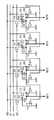
図5は、従来の信号伝送回路の一構成例を示す回路図である。なお、図5には、説明の便宜上、多数段構成のうち4段部分のみを示している。この信号伝送回路は、次段への出力トランジスタT12、T22、T32、T42と、ブートストラップ用容量C1、C2、C3、C4と、ブートストラップ用容量充電トランジスタT11、T21、T31、T41と、放電トランジスタT13、T14、T23、T24、T33、T34、T43、T44とで構成され、電源電圧VDD、駆動パルスV1、V2、およびスタートパルスVSTが供給される。
【0003】
次に、このように構成された従来の信号伝送回路の動作について説明する。
【0004】
スタートパルスVSTが論理「High」レベルになると、初段のブートストラップ用容量充電トランジスタT11がオンになり、ブートストラップ用容量C1が電源電圧VDDへと充電され、ブートストラップ用容量C1の充電電圧が出力トランジスタT12の閾値電圧レベルを超えると、初段の出力トランジスタT12がオンする。
【0005】
その後、論理「High」レベルの駆動パルスV1が出力トランジスタT12のドレインに入力すると、出力トランジスタT12のゲートには、駆動パルスV1の電圧とブートストラップ用容量C1両端の電位差とが足されて印加されることとなり、出力トランジスタT12のゲート電位が駆動パルスV1の電位よりも上昇すると、駆動パルスV1がノードN12から出力パルスOUT1として利用される。
【0006】
また同時に、ノードN12の電圧が、2段目のブートストラップ用容量充電トランジスタT21のゲートに印加されて、トランジスタT21がオンになり、ブートストラップ用容量C2が電源電圧VDDへと充電され、ブートストラップ用容量C2の充電電圧が出力トランジスタT22の閾値電圧レベルを超えると、2段目の出力トランジスタT22がオンする。
【0007】
その後、論理「High」レベルの駆動パルスV2が出力トランジスタT22のドレインに入力すると、出力トランジスタT22のゲートには、駆動パルスV2の電位とブートストラップ用容量C2両端の電位差とが足されて印加されることとなり、出力トランジスタT22のゲート電位が駆動パルスV2の電位よりも上昇すると、駆動パルスV2がノードN22から出力パルスOUT2として利用される。
【0008】
また同時に、ノードN22の電圧が、3段目のブートストラップ用容量充電トランジスタT31のゲートに印加されて、トランジスタT31がオンになり、ブートストラップ用容量C3が電源電圧VDDへと充電され、ブートストラップ用容量C3の充電電圧が出力トランジスタT32の閾値電圧レベルを超えると、3段目の出力トランジスタT22がオンする。
【0009】
このような動作が繰り返されることで、信号伝送回路は、さらに出力パルスOUT3、OUT4と順次出力することになる。
【0010】
【発明が解決しようとする課題】
上記従来の信号伝送回路の問題点について、図6を参照して説明する。
【0011】
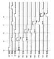
図6は、NMOSのみを用いた従来の信号伝送回路における各部のパルス電圧を示すタイミングチャートである。この回路は5V系の回路であり、駆動パルスV1、V2の電圧振幅、および電源電圧VDDが5Vの場合を示す。
【0012】
図5において、時刻t0において、スタートパルスVSTが5Vに立ち上がると、初段のブートストラップ用容量充電トランジスタT11がオンになり、ブートストラップ用容量C1が電源電圧VDDである5Vに向かって充電されていくが、ここでブートストラップ用容量充電トランジスタT11がエンハンスメント型のNMOSの場合には、トランジスタT11の閾値電圧Vtの影響で、出力トランジスタT12のゲートが接続されたノードN11の電圧VN11は、電源電圧VDDである5VからΔH0だけ低い電圧(5V−ΔH0)となり、この状態で出力トランジスタT12がオンする。
【0013】
次に、時刻t1において、5Vの駆動パルスV1が出力トランジスタT12のドレインに入力すると、出力トランジスタT12のゲート(ノードN11)には、駆動パルスV1の電圧5Vとブートストラップ用容量C1両端の電位差(5V−ΔH0)が加算された電圧HB1が印加され、ノードN12から振幅H1のパルスが出力されることとなる。
【0014】
また同時に、ノードN12の振幅H1のパルス電圧が、2段目のブートストラップ用容量充電トランジスタT21のゲートに印加されて、トランジスタT21がオンになるが、トランジスタT21の閾値電圧VTの影響により、出力トランジスタT22のゲートが接続されたノード21の電圧は、電圧H1からΔH1だけ低い電圧(H1−ΔH1)となり、ブートストラップ用容量C2が電圧(H1−ΔH1)へと充電されることとなる。
【0015】
同様に、時刻t2、t3、t4の場合も、時刻t1の動作を繰り返すこととなる。
【0016】
このように、従来の信号伝送回路の場合、ブートストラップ用容量充電トランジスタのゲートには最大でも5V未満の電圧しか加わらないため、ブートストラップ用容量は、電源電圧VDDである5Vよりも低い電圧にしか充電できないこととなる。したがって、ノードN21、N31、N41の電圧が次第に降下して、信号伝送回路は、何段か先では出力パルスを生成することができなくなる。
【0017】
特に、回路の電源系の低電圧化、たとえば3V系の回路などになると動作がより難しくなる。
【0018】
本発明は、上記の問題点に鑑みてなされたものであり、その目的は、回路電源を低電圧化しても安定な動作が可能で、低消費電力化に適した信号伝送回路、およびかかる信号伝送回路が適用される固体撮像装置、かかる固体撮像装置を搭載したカメラ、および上記信号伝送回路が適用される液晶表示装置を提供することにある。
【0019】
【課題を解決するための手段】
前記の目的を達成するため、本発明に係る信号伝送回路は、複数段回路で構成され、各段回路から駆動パルスに従ったパルス電圧が順次出力される信号伝送回路であって、前記各段回路は、前記駆動パルスを前記パルス電圧としてソースに出力する出力トランジスタと、前記出力トランジスタのゲートとソースとの間に接続されたブートストラップ用容量と、前記ブートストラップ用容量を充電するために、ドレインが電源または接地線に接続され、ソースが前記出力トランジスタのゲートに接続され、2段目以降にはゲートが前段の出力トランジスタのゲートに接続された充電トランジスタとを備えたことを特徴とする。
【0020】
この構成によれば、次段のブートストラップ用容量充電トランジスタのゲートには、従来よりも高い電圧が加わることになり、ブートストラップ用容量充電トランジスタのゲート電位を電源電圧VDDよりも高くすることができる。これにより、次段のブートストラップ用容量を電源電圧VDDに充電することができ、ブートストラップ用容量への充電電圧の降下を防ぐことができる。したがって、伝送段数が増えることにより、出力パルス電圧が次第に低下したり、何段か先で出力パルスが出なくなることを防止することができる。
【0021】
本発明に係る信号伝送回路は、前記各段回路の初段に配置された前記充電トランジスタのゲートにスタートパルスが供給されることが好ましい。
【0022】
本発明に係る信号伝送回路は、ドレインがブートストラップ用容量の一端に接続された第1の放電トランジスタと、ドレインがブートストラップ用容量の他端に接続された第2の放電トランジスタとを備え、第1および第2の放電トランジスタのゲートに共通のパルス電圧が印加されることが好ましい。この場合、共通のパルス電圧は、次段の出力トランジスタのソースから供給されることが好ましい。
【0023】
この構成によれば、放電トランジスタを2個追加するだけで、ブートストラップ用容量の放電ができ、他の外部入力パルスなどが無い規模の小さい回路構成にも本発明を適用することができる。
【0024】
また、本発明に係る信号伝送回路は、ドレインが3段目以降の出力トランジスタのゲートに接続された誤動作防止用トランジスタを備えることが好ましい。
【0025】
この構成によれば、出力トランジスタの閾値電圧が低い場合でも誤動作を防止でき、閾値電圧の範囲を広くとることができる。
【0026】
また、本発明に係る信号伝送回路は、3段目以降の各段回路において、誤動作防止用トランジスタは、ドレインが出力トランジスタのゲートに接続され、ゲートが前々段の出力トランジスタのソースに接続された誤動作防止用トランジスタを備えることが好ましい。
【0027】
この構成によれば、誤動作防止用トランジスタのゲートに前々段の出力トランジスタのソースを接続するように構成したことで、他の外部入力パルスなどが無い規模の小さい回路構成にも本発明を適用することができる。
【0028】
また、充電トランジスタのコンダクタンスが、誤動作防止用トランジスタのコンダクタンスよりも小さいことが好ましい。
【0029】
この構成によれば、ブートストラップ用容量のプラス端子側をより0Vに近づけることができ、誤動作をより確実に防止することができる。
【0030】
または、本発明に係る信号伝送回路において、ある段の出力トランジスタのソースにパルス電圧が出力されている期間、次段の充電トランジスタを動作可能とし、次次段の充電トランジスタを動作禁止にするような電源電圧パルスが次段の前記充電トランジスタのドレイン及び次次段の前記充電トランジスタのドレインのそれぞれに供給されることが好ましい。例えば、充電トランジスタがNMOSからなる場合、電源電圧パルスとして、「High」レベル電圧を次段の充電トランジスタのドレインに供給し、「Low」レベル電圧を次次段の充電トランジスタのドレインに供給する。また、充電トランジスタがPMOSからなる場合、電源電圧パルスとして、「Low」レベル電圧を次段の充電トランジスタのドレインに供給し、「High」レベル電圧を次次段の充電トランジスタのドレインに供給する。
【0031】
この構成によれば、誤動作防止用トランジスタを省略することができ、回路規模を縮小することができる。
【0032】
本発明に係る信号伝送回路において、初段の充電トランジスタのゲートに供給されるスタートパルスの電圧振幅は、駆動パルスの電圧振幅よりも大きいことが好ましい。
【0033】
この構成によれば、初段の充電トランジスタによる電圧降下を防止し、初段のブートストラップ用容量を電源電圧VDDに充電することができる。
【0034】
本発明に係る信号伝送回路において、トランジスタが全てNMOSトランジスタである場合、第1および第2の放電トランジスタのソースおよび誤動作防止用トランジスタのソースのうち少なくとも一方には、接地電位が供給される。
【0035】
または、本発明に係る信号伝送回路において、トランジスタが全てNMOSトランジスタである場合、第1および第2の放電トランジスタのソースおよび誤動作防止用トランジスタのソースには、出力トランジスタの閾値電圧よりも低い電圧が供給される。
【0036】
本発明に係る信号伝送回路において、トランジスタが全てPMOSトランジスタである場合、第1および第2の放電トランジスタのソースおよび誤動作防止用トランジスタのソースのうち少なくとも一方には、電源電圧が供給される。
【0037】
または、本発明に係る信号伝送回路において、トランジスタが全てPMOSトランジスタである場合、第1および第2の放電トランジスタのソースおよび誤動作防止用トランジスタのソースには、出力トランジスタの閾値電圧よりも高い電圧が供給される。
【0038】
前記の目的を達成するため、本発明に係る固体撮像装置は、複数段回路で構成され、各段回路から駆動パルスに従った走査パルス電圧が順次出力される信号伝送回路を有する固体撮像装置であって、前記信号伝送回路の各段回路は、前記駆動パルスを前記走査パルス電圧としてソースに出力する出力トランジスタと、前記出力トランジスタのゲートとソースとの間に接続されたブートストラップ用容量と、前記ブートストラップ用容量を充電するために、ドレインが電源または接地線に接続され、ソースが前記出力トランジスタのゲートに接続され、ソースが前記出力トランジスタのゲートに接続され、2段目以降にはゲートが前段の出力トランジスタのゲートに接続された充電トランジスタとを備えたことを特徴とする。
【0039】
本発明に係る固体撮像装置は、前記各段回路の初段に配置された前記充電トランジスタのゲートにスタートパルスが供給されることが好ましい。
【0040】
前記の目的を達成するため、本発明に係るカメラは、本発明に係る固体撮像装置を搭載したことを特徴とする。
【0041】
前記の目的を達成するため、本発明に係る液晶表示装置は、複数段回路で構成され、各段回路から駆動パルスに従った走査パルス電圧が順次出力される信号伝送回路を有する液晶表示装置であって、前記信号伝送回路の各段回路は、前記駆動パルスを前記走査パルス電圧としてソースに出力する出力トランジスタと、前記出力トランジスタのゲートとソースとの間に接続されたブートストラップ用容量と、前記ブートストラップ用容量を充電するために、ドレインが電源または接地線に接続され、ソースが前記出力トランジスタのゲートに接続され、ソースが前記出力トランジスタのゲートに接続され、2段目以降にはゲートが前段の出力トランジスタのゲートに接続された充電トランジスタとを備えたことを特徴とする。
【0042】
本発明に係る液晶表示装置は、前記各段回路の初段に配置された前記充電トランジスタのゲートにスタートパルスが供給されることが好ましい。
【0043】
上記の構成によれば、回路電源を低電圧化しても安定な動作を保証することができ、特に低消費電力化を図る必要のある携帯用機器に適用される、固体撮像装置、それを搭載したカメラ、および液晶表示装置において効果を発揮することができる。
【0044】
【発明の実施の形態】
以下、本発明の好適な実施の形態について、図面を参照して説明する。
【0045】
図1は、本発明の第1の実施形態に係る信号伝送回路の一構成例を示す回路図である。なお、本実施形態が図5に示す従来例と異なる点は、前段の出力トランジスタのゲートが次段のブートストラップ用容量充電トランジスタのゲートに接続されている点にある。その他の構成については、図5の従来例と同じであり、図1において同一の符号を付す。
【0046】
図1において、スタートパルスVSTが論理「High」レベルになると、初段のブートストラップ用容量充電トランジスタT11がオンになり、ブートストラップ用容量C1が電源電圧VDDへと充電され、ブートストラップ用容量C1の充電電圧が出力トランジスタT12の閾値電圧レベルを超えると、初段の出力トランジスタT12がオンする。
【0047】
その後、論理「High」レベルの駆動パルスV1が出力トランジスタT12のドレインに入力すると、出力トランジスタT12のゲートには、駆動パルスV1の電圧とブートストラップ用容量C1両端の電位差とが足されて印加されることとなり、出力トランジスタT12のゲート電位が駆動パルスV1の電位よりも上昇すると、駆動パルスV1が初段の出力ノードN12から出力パルスOUT1として利用される。
【0048】
ここで、本実施形態による信号伝送回路の利点は、ブートストラップ用容量C1のプラス側の端子に接続されたノードN11の電圧が、2段目のブートストラップ用容量充電トランジスタT21のゲートに印加されるため、トランジスタT21のゲートに高い電圧を印加することができる点にある。これによって、2段目のブートストラップ用容量充電トランジスタT21が、たとえエンハンスメント型のNMOSであっても、ブートストラップ用容量C21を電源電圧VDDに確実に充電でき、出力トランジスタT22をオンにすることができる。
【0049】
その後、論理「High」レベルの駆動パルスV2が出力トランジスタT22のドレインに入力すると、出力トランジスタT22のゲートには、駆動パルスV2の電位とブートストラップ用容量C2両端の電位差とが足されて印加されることとなり、出力トランジスタT22のゲート電位が駆動パルスV2の電位よりも上昇すると、駆動パルスV2が2段目の出力ノードN22から出力パルスOUT2として利用される。
【0050】
また同時に、ブートストラップ用容量C2のプラス側の端子に接続されたノードN21の高い電圧が、3段目のブートストラップ用容量充電トランジスタT31のゲートに印加され、トランジスタT31がオンになり、ブートストラップ用容量C3が電源電圧VDDに確実に充電され、出力トランジスタT32がオンする。
【0051】
このような動作が繰り返されることで、信号伝送回路は、さらに出力パルスOUT3、OUT4と順次出力することになる。
【0052】
このようにして、全ての信号伝送段において、ブートストラップ用容量のプラス側の端子電圧が、次段のブートストラップ用容量充電トランジスタのゲートに加わるため、次段のブートストラップ用容量を確実に電源電圧VDDに充電できることとなり、電圧降下の無い低電圧の出力パルスを生成可能な信号伝送回路を実現できる。
【0053】
また、ブートストラップ用容量に充電した電圧を放電する手段として、回路のトランジスタや電源を少なくするために、ブートストラップ用容量C1の場合は、放電トランジスタT13のドレインをブートストラップ用容量C1のプラス側端子に接続し、放電トランジスタT14のドレインをブートストラップ用容量C1のマイナス側端子に接続し、放電トランジスタT13およびT14のゲートに、2段目の出力トランジスタT22のソースに接続された出力ノードN22を接続する。これにより、2段目の出力ノードN22に駆動パルスV2が出力された時に、ブートストラップ用容量C1が放電されることになる。
【0054】
この構成により、放電トランジスタを2個追加するだけで、ブートストラップ用容量の放電ができ、他の外部入力パルスなどが無い規模の小さい回路構成でも、本実施形態の信号伝送回路を実現することができる。
【0055】
なお、図2に示すように、ブートストラップ用容量のマイナス側の放電は、従来と同様に、駆動パルスV1またはV2を用いて行ってもよい。
【0056】
図3は、NMOSのみを用いた図1の信号伝送回路における各部のパルス電圧を示すタイミングチャートである。この回路は3V系の回路であり、駆動パルスV1、V2の電圧振幅、および電源電圧VDDが3Vの場合を示す。ただし、スタートパルスVSTの電圧振幅は5Vとする。ここで、スタートパルスVSTの電圧振幅のみ5Vとするのは、スタートパルスVSTが入力される初段のブートストラップ用容量充電トランジスタT11の場合のみ、前段からの高い電圧が供給できないため、スタートパルスVSTのみ駆動パルスV1、V2の電圧振幅である3Vよりも高い5VでトランジスタT11を駆動することにより、トランジスタT11による電圧降下を防止し、ブートストラップ用容量C1を電源電圧VDDである3Vに充電可能にするためである。
【0057】
図3において、時刻t0において、スタートパルスVSTの電圧が5Vに立ち上がり、エンハンスメント型のNMOSであるブートストラップ用容量充電トランジスタT11の閾値電圧Vtがあった場合でも、トランジスタT11を介してブートストラップ用容量C1が電源電圧VDDである3Vに充電され、出力トランジスタT12がオンする。
【0058】
次に、時刻t1において、駆動パルスV1が3Vに立ち上がり、出力トランジスタT12のドレインに入力すると、出力トランジスタT12のゲートには、駆動パルスV1の電圧3Vとブートストラップ用容量C1両端の電位差3Vとが足された高い電圧HB1電圧が印加されるめ、出力ノードN12から3V振幅の駆動パルスV1が出力パルスOUT1として確実に出力されることになる。
【0059】
また同時に、ブートストラップ用容量C1のプラス側の端子に接続されたノードN11の高電圧HB1が、2段目のブートストラップ用容量充電トランジスタT21のゲートに入力され、トランジスタT21がオンして、ブートストラップ用容量C2が確実に電源電圧VDDである3Vに充電されることになる。
【0060】
同様にして、時刻t2、t3、t4の場合も、時刻t1の動作を繰り返すこととなる。
【0061】
以上のように、本実施形態によれば、次段のブートストラップ用容量充電トランジスタのゲートには常に、前段のブートストラップ用容量のプラス側の端子電圧が加わるため、次段のブートストラップ用容量を確実に電源電圧3Vに充電できることとなり、電圧降下の無い、3Vの低電圧の出力パルスを生成可能な信号伝送回路を実現できる。
【0062】
(第2の実施形態)
図4は、本発明の第2の実施形態に係る信号伝送回路の一構成例を示す回路図である。第2の実施形態が第1の実施形態と異なる点は、ブートストラップ用容量のプラス側端子に誤動作防止用トランジスタ(T35、T45)を追加した点にある。以下、この相違点についてのみ説明する。
【0063】
2段目のブートストラップ用容量C2が3Vに充電された時、エンハンスメント型のNMOSであるブートストラップ用容量充電トランジスタT31の閾値電圧が低い場合には、ブートストラップ用容量C2のプラス側の端子に接続されたノードN21(3V)がゲートに接続されているブートストラップ用容量充電トランジスタT31がオンして、3段目のブートストラップ用容量C3が3V以下の低い電圧に充電される可能性がある。この状態では、駆動パルスV1が論理「High」レベルである3Vの場合、初段の出力ノードN12に駆動パルスV1が出力されている時に、同時に3段目の出力ノードN32にも駆動パルスV1が出力される可能性がある。
【0064】
そのため、図4に示すように、ブートストラップ用容量C3のプラス端子側を接地電位に近づけて、3段目の出力トランジスタT32がオフするように、ブートストラップ用容量C3のプラス端子側と接地電位との間に、誤動作防止用トランジスタT35を接続した。すなわち、誤動作防止用トランジスタT35のドレインをブートストラップ用容量C3のプラス側に、ソースを接地電位に、ゲートを初段の出力ノードN12に接続し、初段の出力ノードN12に駆動パルスV1が出ている時に誤動作防止用トランジスタをオンして、ノードN31を0V付近にして、3段目の出力ノードN32に駆動パルスV1が出ないようにする。
【0065】
このとき、ブートストラップ用容量充電トランジスタT31のコンダクタンスを誤動作防止用トランジスタT35のコンダクタンスよりも小さくすることで、ブートストラップ用容量C3のプラス端子側をより0Vに近づけることができ、誤動作をより確実に防止することができる。
【0066】
同様に、後段のブートストラップ用容量C4のプラス端子側と接地電位との間にも、それぞれ、誤動作防止用トランジスタT45のドレインとソースを接続し、ゲートには前々段の出力ノードN22を接続することで、全段にわたって誤動作を防止することができる。
【0067】
以上のように、本実施形態によれば、誤動作防止用トランジスタを設けることで、出力トランジスタの閾値電圧が低い場合でも誤動作を防止でき、閾値電圧の範囲を広くとることができる。
【0068】
また、誤動作防止用トランジスタのゲートに前々段の出力トランジスタのソースを接続するように構成したことで、他の外部入力パルスなどが無い規模の小さい回路構成の場合でも、本実施形態による信号伝送回路を実現することができる。
【0069】
なお、第1および第2の実施形態では、放電トランジスタおよび誤動作防止用トランジスタのそれぞれのソースは接地電位(0V)としているが、各ソース電圧は、出力トランジスタの閾値電圧よりも小さい値であれば、0Vでなくても同様の効果が得られる。
【0070】
また、第1および第2の実施形態では、ブートストラップ用容量充電トランジスタのドレインには、電源電圧VDDとしてDC電圧が印加されるため、誤動作が起こる可能性が発生し、誤動作防止用トランジスタを組み込む必要があるが、ブートストラップ用容量充電トランジスタのドレインに、電源電圧VDDとしてパルス電圧を印加することで誤動作を防止することができる。すなわち、出力トランジスタのソースに出力電圧が発生している期間、次段のブートストラップ容量充電トランジスタのドレインを「High」レベルとし、次次段のブートストラップ容量充電トランジスタのドレインを「Low」レベルにすることで、誤動作防止用トランジスタを省略することができる。
【0071】
また、第1および第2の実施形態では、NMOSトランジスタの場合について例示および説明したが、全てPMOSトランジスタである場合についても、同様な効果を得ることができる。
【0072】
【発明の効果】
以上説明したように、本発明によれば、次段のブートストラップ用容量を電源電圧VDDに充電することができ、ブートストラップ用容量への充電電圧の降下を防ぐことができる。したがって、伝送段数が増えることにより、出力パルス電圧が次第に低下したり、何段か先で出力パルスが出なくなることを防止することができる。これによって、安定な低電圧駆動が可能な信号伝送回路を実現することができる。
【0073】
また、かかる信号伝送回路は、液晶デイスプレイ、MOS型撮像装置の低電圧駆動実現の要請に沿いながら、信号伝送回路をシフトレジスタに使用して、低電圧化を実現とするものであって、産業上極めて有用である。
【図面の簡単な説明】
【図1】 本発明の第1の実施形態に係る信号伝送回路の一構成例を示す回路図
【図2】 本発明の第1の実施形態に係る信号伝送回路の他の構成例を示す回路図
【図3】 本発明の第1の実施形態に係る信号伝送回路における各部のパルス電圧を示すタイミングチャート
【図4】 本発明の第2の実施形態に係る信号伝送回路の一構成例を示す回路図
【図5】 従来の信号伝送回路の一構成例を示す回路図
【図6】 従来の信号伝送回路における各部のパルス電圧を示すタイミングチャート
【符号の説明】
C1、C2、C3、C4 ブートストラップ用容量
OUT1、OUT2、OUT3、OUT4 出力パルス(走査パルス)
T11、T21、T31、T41 ブートストラップ用容量充電トランジスタ(充電トランジスタ)
T12、T22、T32、T42 出力トランジスタ
T13、T23、T33、T43 放電トランジスタ(第1の放電トランジスタ)
T14、T24、T34、T44 放電トランジスタ(第2の放電トランジスタ)
T35、T45 誤動作防止用トランジスタ
V1、V2 駆動パルス
VDD 電源電圧
VST スタートパルス[0001]
BACKGROUND OF THE INVENTION
The present invention relates to a signal transmission circuit that is applied to a shift register for driving a liquid crystal display and a MOS type imaging device and can be driven at a low voltage.
[0002]
[Prior art]
FIG. 5 is a circuit diagram showing a configuration example of a conventional signal transmission circuit. For convenience of explanation, FIG. 5 shows only the four-stage portion of the multistage configuration. This signal transmission circuit includes output transistors T12, T22, T32, T42 to the next stage, bootstrap capacitors C1, C2, C3, C4, bootstrap capacitor charging transistors T11, T21, T31, T41, and discharge. The transistors T13, T14, T23, T24, T33, T34, T43, and T44 are supplied with a power supply voltage VDD, drive pulses V1 and V2, and a start pulse VST.
[0003]
Next, the operation of the conventional signal transmission circuit configured as described above will be described.
[0004]
When the start pulse VST becomes a logic “High” level, the bootstrap capacitor charging transistor T11 in the first stage is turned on, the bootstrap capacitor C1 is charged to the power supply voltage VDD, and the charge voltage of the bootstrap capacitor C1 is output. When the threshold voltage level of the transistor T12 is exceeded, the first-stage output transistor T12 is turned on.
[0005]
After that, when the driving pulse V1 having the logic “High” level is input to the drain of the output transistor T12, the voltage of the driving pulse V1 and the potential difference between both ends of the bootstrap capacitor C1 are applied to the gate of the output transistor T12. Thus, when the gate potential of the output transistor T12 rises higher than the potential of the drive pulse V1, the drive pulse V1 is used as the output pulse OUT1 from the node N12.
[0006]
At the same time, the voltage of the node N12 is applied to the gate of the second-stage bootstrap capacitor charging transistor T21, the transistor T21 is turned on, and the bootstrap capacitor C2 is charged to the power supply voltage VDD. When the charging voltage of the capacitor C2 exceeds the threshold voltage level of the output transistor T22, the second-stage output transistor T22 is turned on.
[0007]
After that, when the drive pulse V2 having the logic “High” level is input to the drain of the output transistor T22, the potential of the drive pulse V2 and the potential difference between both ends of the bootstrap capacitor C2 are applied to the gate of the output transistor T22. Thus, when the gate potential of the output transistor T22 rises higher than the potential of the drive pulse V2, the drive pulse V2 is used as the output pulse OUT2 from the node N22.
[0008]
At the same time, the voltage of the node N22 is applied to the gate of the third stage bootstrap capacitor charging transistor T31, the transistor T31 is turned on, and the bootstrap capacitor C3 is charged to the power supply voltage VDD. When the charging voltage of the capacitor C3 exceeds the threshold voltage level of the output transistor T32, the third-stage output transistor T22 is turned on.
[0009]
By repeating such an operation, the signal transmission circuit further sequentially outputs output pulses OUT3 and OUT4.
[0010]
[Problems to be solved by the invention]
The problems of the conventional signal transmission circuit will be described with reference to FIG.
[0011]
FIG. 6 is a timing chart showing pulse voltages at various parts in a conventional signal transmission circuit using only NMOS. This circuit is a 5V circuit, and shows the case where the voltage amplitudes of the drive pulses V1 and V2 and the power supply voltage VDD are 5V.
[0012]
In FIG. 5, when the start pulse VST rises to 5V at time t0, the first stage bootstrap capacitor charging transistor T11 is turned on, and the bootstrap capacitor C1 is charged toward 5V which is the power supply voltage VDD. However, when the bootstrap capacitive charging transistor T11 is an enhancement type NMOS, the voltage VN11 of the node N11 to which the gate of the output transistor T12 is connected is affected by the threshold voltage Vt of the transistor T11. The voltage is lowered by 5H from Δ5V (5V-ΔH0), and the output transistor T12 is turned on in this state.
[0013]
Next, when a 5V drive pulse V1 is input to the drain of the output transistor T12 at time t1, the voltage difference between the
[0014]
At the same time, a pulse voltage having an amplitude H1 at the node N12 is applied to the gate of the second-stage bootstrap capacitive charging transistor T21 to turn on the transistor T21. However, the output is affected by the threshold voltage VT of the transistor T21. The voltage of the node 21 to which the gate of the transistor T22 is connected becomes a voltage (H1−ΔH1) lower than the voltage H1 by ΔH1, and the bootstrap capacitor C2 is charged to the voltage (H1−ΔH1).
[0015]
Similarly, at times t2, t3, and t4, the operation at time t1 is repeated.
[0016]
As described above, in the case of the conventional signal transmission circuit, only a voltage less than 5 V is applied to the gate of the bootstrap capacitance charging transistor, so that the bootstrap capacitance is set to a voltage lower than the power supply voltage VDD of 5 V. It can only be charged. Accordingly, the voltages at the nodes N21, N31, and N41 gradually drop, and the signal transmission circuit cannot generate an output pulse several steps ahead.
[0017]
In particular, the operation becomes more difficult when the voltage of the power supply system of the circuit is lowered, for example, a 3V circuit or the like.
[0018]
The present invention has been made in view of the above problems, and an object of the present invention is to provide a signal transmission circuit suitable for low power consumption, capable of stable operation even when the circuit power supply is lowered, and such a signal. An object of the present invention is to provide a solid-state imaging device to which a transmission circuit is applied, a camera equipped with the solid-state imaging device, and a liquid crystal display device to which the signal transmission circuit is applied.
[0019]
[Means for Solving the Problems]
In order to achieve the above object, a signal transmission circuit according to the present invention is a signal transmission circuit configured by a plurality of stage circuits, in which a pulse voltage according to a driving pulse is sequentially output from each stage circuit. The circuit outputs an output transistor that outputs the drive pulse as the pulse voltage to a source, a bootstrap capacitor connected between a gate and a source of the output transistor, and a capacitor for charging the bootstrap capacitor. The drain is connected to the power supply or ground line, and the source is connected to the gate of the output transistor.2After stageInAnd a charging transistor having a gate connected to the gate of the output transistor in the previous stage.
[0020]
According to this configuration, a higher voltage is applied to the gate of the bootstrap capacitive charging transistor in the next stage, and the gate potential of the bootstrap capacitive charging transistor can be made higher than the power supply voltage VDD. it can. As a result, the bootstrap capacitor at the next stage can be charged to the power supply voltage VDD, and a drop in the charging voltage to the bootstrap capacitor can be prevented. Therefore, the increase in the number of transmission stages can prevent the output pulse voltage from gradually decreasing or the output pulse from not being output several stages earlier.
[0021]
In the signal transmission circuit according to the present invention, it is preferable that a start pulse is supplied to the gate of the charging transistor arranged in the first stage of each stage circuit.
[0022]
A signal transmission circuit according to the present invention includes a first discharge transistor having a drain connected to one end of a bootstrap capacitor, and a second discharge transistor having a drain connected to the other end of the bootstrap capacitor, A common pulse voltage is preferably applied to the gates of the first and second discharge transistors. In this case, the common pulse voltage is preferably supplied from the source of the output transistor at the next stage.
[0023]
According to this configuration, the bootstrap capacitor can be discharged by adding only two discharge transistors, and the present invention can be applied to a small circuit configuration without other external input pulses.
[0024]
The signal transmission circuit according to the present invention preferably includes a malfunction prevention transistor whose drain is connected to the gate of the output transistor in the third and subsequent stages.
[0025]
According to this configuration, malfunction can be prevented even when the threshold voltage of the output transistor is low, and the range of the threshold voltage can be widened.
[0026]
In the signal transmission circuit according to the present invention, in each of the third and subsequent stages, the malfunction prevention transistor has a drain connected to the gate of the output transistor and a gate connected to the source of the output transistor in the preceding stage. It is preferable to provide a malfunction prevention transistor.
[0027]
According to this configuration, the present invention can be applied to a small circuit configuration without other external input pulses by connecting the source of the output transistor in the previous stage to the gate of the malfunction prevention transistor. can do.
[0028]
Further, it is preferable that the conductance of the charging transistor is smaller than the conductance of the malfunction preventing transistor.
[0029]
According to this configuration, the positive terminal side of the bootstrap capacitor can be brought closer to 0 V, and malfunction can be prevented more reliably.
[0030]
Alternatively, in the signal transmission circuit according to the present invention, during the period in which the pulse voltage is output to the source of the output transistor at a certain stage, the charging transistor at the next stage can be operated and the charging transistor at the next stage is disabled. Power supply voltage pulseTo the drain of the charging transistor in the next stage and the drain of the charging transistor in the next stagePreferably it is supplied. For example, when the charging transistor is composed of NMOS, as the power supply voltage pulse, the “High” level voltage is supplied to the drain of the next stage charging transistor, and the “Low” level voltage is supplied to the drain of the next stage charging transistor. Further, when the charging transistor is composed of PMOS, as the power supply voltage pulse, the “Low” level voltage is supplied to the drain of the next stage charging transistor, and the “High” level voltage is supplied to the drain of the next stage charging transistor.
[0031]
According to this configuration, the malfunction prevention transistor can be omitted, and the circuit scale can be reduced.
[0032]
In the signal transmission circuit according to the present invention, it is preferable that the voltage amplitude of the start pulse supplied to the gate of the first-stage charging transistor is larger than the voltage amplitude of the drive pulse.
[0033]
According to this configuration, it is possible to prevent a voltage drop due to the first-stage charging transistor and to charge the first-stage bootstrap capacitor to the power supply voltage VDD.
[0034]
In the signal transmission circuit according to the present invention, when all the transistors are NMOS transistors, a ground potential is supplied to at least one of the sources of the first and second discharge transistors and the malfunction prevention transistor.
[0035]
Alternatively, in the signal transmission circuit according to the present invention, when all the transistors are NMOS transistors, a voltage lower than the threshold voltage of the output transistor is applied to the sources of the first and second discharge transistors and the malfunction prevention transistor. Supplied.
[0036]
In the signal transmission circuit according to the present invention, when all the transistors are PMOS transistors, a power supply voltage is supplied to at least one of the sources of the first and second discharge transistors and the malfunction prevention transistor.
[0037]
Alternatively, in the signal transmission circuit according to the present invention, when all the transistors are PMOS transistors, a voltage higher than the threshold voltage of the output transistor is applied to the sources of the first and second discharge transistors and the malfunction prevention transistor. Supplied.
[0038]
In order to achieve the above object, a solid-state imaging device according to the present invention is a solid-state imaging device having a signal transmission circuit configured by a plurality of stage circuits and sequentially outputting a scanning pulse voltage from each stage circuit according to a driving pulse. Each stage circuit of the signal transmission circuit includes an output transistor that outputs the drive pulse to the source as the scan pulse voltage, a bootstrap capacitor connected between the gate and the source of the output transistor, In order to charge the bootstrap capacitor, the drain is connected to a power supply or a ground line, the source is connected to the gate of the output transistor, and the source is connected to the gate of the output transistor.2After stageInAnd a charging transistor having a gate connected to the gate of the output transistor in the previous stage.
[0039]
In the solid-state imaging device according to the present invention, it is preferable that a start pulse is supplied to the gate of the charging transistor arranged in the first stage of each stage circuit.
[0040]
In order to achieve the above object, a camera according to the present invention includes the solid-state imaging device according to the present invention.
[0041]
In order to achieve the above object, a liquid crystal display device according to the present invention is a liquid crystal display device having a signal transmission circuit that is configured by a plurality of stage circuits and that sequentially outputs a scanning pulse voltage according to a drive pulse from each stage circuit. Each stage circuit of the signal transmission circuit includes an output transistor that outputs the drive pulse to the source as the scan pulse voltage, a bootstrap capacitor connected between the gate and the source of the output transistor, In order to charge the bootstrap capacitor, the drain is connected to a power supply or a ground line, the source is connected to the gate of the output transistor, and the source is connected to the gate of the output transistor.2After stageInAnd a charging transistor having a gate connected to the gate of the output transistor in the previous stage.
[0042]
In the liquid crystal display device according to the present invention, it is preferable that a start pulse is supplied to the gate of the charging transistor arranged in the first stage of each stage circuit.
[0043]
According to the above configuration, a stable operation can be ensured even when the voltage of the circuit power supply is lowered, and the solid-state imaging device, which is applied to a portable device that particularly needs to reduce power consumption, is mounted. The effect can be exhibited in the camera and the liquid crystal display device.
[0044]
DETAILED DESCRIPTION OF THE INVENTION
DESCRIPTION OF EXEMPLARY EMBODIMENTS Hereinafter, preferred embodiments of the invention will be described with reference to the drawings.
[0045]
FIG. 1 is a circuit diagram showing a configuration example of a signal transmission circuit according to the first embodiment of the present invention. The present embodiment is different from the conventional example shown in FIG. 5 in that the gate of the output transistor at the previous stage is connected to the gate of the capacitive charging transistor for bootstrap at the next stage. Other configurations are the same as those of the conventional example of FIG. 5, and the same reference numerals are given in FIG.
[0046]
In FIG. 1, when the start pulse VST becomes a logic “High” level, the bootstrap capacitor charging transistor T11 in the first stage is turned on, and the bootstrap capacitor C1 is charged to the power supply voltage VDD. When the charging voltage exceeds the threshold voltage level of the output transistor T12, the first-stage output transistor T12 is turned on.
[0047]
After that, when the driving pulse V1 having the logic “High” level is input to the drain of the output transistor T12, the voltage of the driving pulse V1 and the potential difference between both ends of the bootstrap capacitor C1 are applied to the gate of the output transistor T12. Thus, when the gate potential of the output transistor T12 rises higher than the potential of the drive pulse V1, the drive pulse V1 is used as the output pulse OUT1 from the output node N12 in the first stage.
[0048]
Here, the advantage of the signal transmission circuit according to the present embodiment is that the voltage of the node N11 connected to the positive terminal of the bootstrap capacitor C1 is applied to the gate of the bootstrap capacitor charging transistor T21 at the second stage. Therefore, a high voltage can be applied to the gate of the transistor T21. As a result, even if the second-stage bootstrap capacitor charging transistor T21 is an enhancement type NMOS, the bootstrap capacitor C21 can be reliably charged to the power supply voltage VDD, and the output transistor T22 can be turned on. it can.
[0049]
After that, when the drive pulse V2 having the logic “High” level is input to the drain of the output transistor T22, the potential of the drive pulse V2 and the potential difference between both ends of the bootstrap capacitor C2 are applied to the gate of the output transistor T22. Thus, when the gate potential of the output transistor T22 rises above the potential of the drive pulse V2, the drive pulse V2 is used as the output pulse OUT2 from the second-stage output node N22.
[0050]
At the same time, a high voltage at the node N21 connected to the positive terminal of the bootstrap capacitor C2 is applied to the gate of the third-stage bootstrap capacitor charging transistor T31, turning on the transistor T31. The capacitor C3 is reliably charged to the power supply voltage VDD, and the output transistor T32 is turned on.
[0051]
By repeating such an operation, the signal transmission circuit further sequentially outputs output pulses OUT3 and OUT4.
[0052]
In this way, in all signal transmission stages, the positive terminal voltage of the bootstrap capacitor is applied to the gate of the next bootstrap capacitor charging transistor, so that the next bootstrap capacitor can be reliably powered. Since the voltage VDD can be charged, a signal transmission circuit capable of generating a low-voltage output pulse with no voltage drop can be realized.
[0053]
Further, as a means for discharging the voltage charged in the bootstrap capacitor, in order to reduce circuit transistors and power supplies, in the case of the bootstrap capacitor C1, the drain of the discharge transistor T13 is connected to the positive side of the bootstrap capacitor C1. The drain of the discharge transistor T14 is connected to the negative terminal of the bootstrap capacitor C1, and the output node N22 connected to the source of the second-stage output transistor T22 is connected to the gates of the discharge transistors T13 and T14. Connecting. As a result, when the drive pulse V2 is output to the output node N22 in the second stage, the bootstrap capacitor C1 is discharged.
[0054]
With this configuration, the bootstrap capacitor can be discharged by adding only two discharge transistors, and the signal transmission circuit of this embodiment can be realized even in a small circuit configuration without other external input pulses. it can.
[0055]
As shown in FIG. 2, the discharge on the negative side of the bootstrap capacitor may be performed using the drive pulse V1 or V2 as in the conventional case.
[0056]
FIG. 3 is a timing chart showing pulse voltages at various parts in the signal transmission circuit of FIG. 1 using only NMOS. This circuit is a 3V system circuit, and shows the case where the voltage amplitudes of the drive pulses V1 and V2 and the power supply voltage VDD are 3V. However, the voltage amplitude of the start pulse VST is 5V. Here, only the voltage amplitude of the start pulse VST is set to 5 V. Only in the case of the first-stage bootstrap capacitive charging transistor T11 to which the start pulse VST is input, a high voltage from the previous stage cannot be supplied, so only the start pulse VST is set. By driving the transistor T11 with 5V higher than the
[0057]
In FIG. 3, even when the voltage of the start pulse VST rises to 5 V at time t0 and there is a threshold voltage Vt of the bootstrap capacitive charging transistor T11 that is an enhancement type NMOS, the bootstrap capacitance is passed through the transistor T11. C1 is charged to 3V which is the power supply voltage VDD, and the output transistor T12 is turned on.
[0058]
Next, at time t1, when the drive pulse V1 rises to 3V and is input to the drain of the output transistor T12, the
[0059]
At the same time, the high voltage HB1 of the node N11 connected to the positive terminal of the bootstrap capacitor C1 is input to the gate of the second-stage bootstrap capacitor charging transistor T21, turning on the transistor T21 and The strap capacitor C2 is reliably charged to 3 V, which is the power supply voltage VDD.
[0060]
Similarly, at times t2, t3, and t4, the operation at time t1 is repeated.
[0061]
As described above, according to the present embodiment, the terminal voltage on the positive side of the bootstrap capacitor in the previous stage is always applied to the gate of the bootstrap capacitor charging transistor in the next stage. Can be reliably charged to the
[0062]
(Second Embodiment)
FIG. 4 is a circuit diagram showing a configuration example of a signal transmission circuit according to the second embodiment of the present invention. The second embodiment is different from the first embodiment in that a malfunction prevention transistor (T35, T45) is added to the positive side terminal of the bootstrap capacitor. Only this difference will be described below.
[0063]
When the bootstrap capacitor C2 in the second stage is charged to 3V, if the threshold voltage of the bootstrap capacitor charging transistor T31, which is an enhancement type NMOS, is low, the positive side terminal of the bootstrap capacitor C2 is connected to the positive side. There is a possibility that the bootstrap capacitor charging transistor T31 connected to the gate of the connected node N21 (3V) is turned on and the third stage bootstrap capacitor C3 is charged to a low voltage of 3V or less. . In this state, when the driving pulse V1 is 3V which is the logic “High” level, when the driving pulse V1 is output to the first-stage output node N12, the driving pulse V1 is also output to the third-stage output node N32 at the same time. There is a possibility that.
[0064]
Therefore, as shown in FIG. 4, the positive terminal side of the bootstrap capacitor C3 and the ground potential are set so that the positive terminal side of the bootstrap capacitor C3 is brought close to the ground potential and the third-stage output transistor T32 is turned off. A malfunction prevention transistor T35 is connected between the two. That is, the drain of the malfunction prevention transistor T35 is connected to the plus side of the bootstrap capacitor C3, the source is connected to the ground potential, the gate is connected to the first-stage output node N12, and the drive pulse V1 is output to the first-stage output node N12. Occasionally, the malfunction prevention transistor is turned on so that the node N31 is close to 0V so that the drive pulse V1 is not output to the third-stage output node N32.
[0065]
At this time, by making the conductance of the bootstrap capacitor charging transistor T31 smaller than the conductance of the malfunction prevention transistor T35, the plus terminal side of the bootstrap capacitor C3 can be brought closer to 0V, and the malfunction is more reliably performed. Can be prevented.
[0066]
Similarly, the drain and source of the malfunction prevention transistor T45 are connected between the positive terminal side of the bootstrap capacitor C4 at the subsequent stage and the ground potential, respectively, and the output node N22 at the preceding stage is connected to the gate. By doing so, it is possible to prevent malfunctions in all stages.
[0067]
As described above, according to this embodiment, by providing the malfunction prevention transistor, malfunction can be prevented even when the threshold voltage of the output transistor is low, and the threshold voltage range can be widened.
[0068]
In addition, since the source of the output transistor in the previous stage is connected to the gate of the malfunction prevention transistor, signal transmission according to this embodiment is possible even in the case of a small circuit configuration without other external input pulses. A circuit can be realized.
[0069]
In the first and second embodiments, the respective sources of the discharge transistor and the malfunction prevention transistor are set to the ground potential (0 V), but each source voltage is a value smaller than the threshold voltage of the output transistor. Even if it is not 0 V, the same effect can be obtained.
[0070]
In the first and second embodiments, since a DC voltage is applied as the power supply voltage VDD to the drain of the bootstrap capacitive charging transistor, a malfunction may occur, and a malfunction prevention transistor is incorporated. Although necessary, a malfunction can be prevented by applying a pulse voltage as the power supply voltage VDD to the drain of the bootstrap capacitive charging transistor. That is, during the period when the output voltage is generated at the source of the output transistor, the drain of the bootstrap capacitor charging transistor at the next stage is set to “High” level, and the drain of the bootstrap capacitor charging transistor at the next stage is set to “Low” level. Thus, the malfunction prevention transistor can be omitted.
[0071]
Further, in the first and second embodiments, the case of the NMOS transistor is illustrated and described, but the same effect can be obtained even in the case of all the PMOS transistors.
[0072]
【The invention's effect】
As described above, according to the present invention, the bootstrap capacitor at the next stage can be charged to the power supply voltage VDD, and a drop in the charging voltage to the bootstrap capacitor can be prevented. Therefore, the increase in the number of transmission stages can prevent the output pulse voltage from gradually decreasing or the output pulse from not being output several stages earlier. As a result, a signal transmission circuit capable of stable low-voltage driving can be realized.
[0073]
In addition, such a signal transmission circuit achieves a low voltage by using a signal transmission circuit as a shift register in line with a request for realizing a low voltage drive of a liquid crystal display and a MOS type imaging device. It is extremely useful.
[Brief description of the drawings]
FIG. 1 is a circuit diagram showing a configuration example of a signal transmission circuit according to a first embodiment of the present invention.
FIG. 2 is a circuit diagram showing another configuration example of the signal transmission circuit according to the first embodiment of the present invention.
FIG. 3 is a timing chart showing pulse voltages at various parts in the signal transmission circuit according to the first embodiment of the present invention.
FIG. 4 is a circuit diagram showing a configuration example of a signal transmission circuit according to a second embodiment of the present invention.
FIG. 5 is a circuit diagram showing a configuration example of a conventional signal transmission circuit.
FIG. 6 is a timing chart showing pulse voltages at various parts in a conventional signal transmission circuit.
[Explanation of symbols]
C1, C2, C3, C4 Bootstrap capacity
OUT1, OUT2, OUT3, OUT4 Output pulse (scanning pulse)
T11, T21, T31, T41 Capacitor charge transistor for bootstrap (charge transistor)
T12, T22, T32, T42 Output transistor
T13, T23, T33, T43 Discharge transistor (first discharge transistor)
T14, T24, T34, T44 Discharge transistor (second discharge transistor)
T35, T45 Malfunction prevention transistor
V1, V2 drive pulse
VDD supply voltage
VST start pulse
Claims (22)
Translated fromJapanese前記駆動パルスを前記パルス電圧としてソースに出力する出力トランジスタと、
前記出力トランジスタのゲートとソースとの間に接続されたブートストラップ用容量と、
前記ブートストラップ用容量を充電するために、ドレインが電源または接地線に接続され、ソースが前記出力トランジスタのゲートに接続され、2段目以降にはゲートが前段の出力トランジスタのゲートに接続された充電トランジスタとを備えたことを特徴とする信号伝送回路。A signal transmission circuit composed of a plurality of stage circuits and sequentially outputting a pulse voltage in accordance with a driving pulse from each stage circuit, wherein each stage circuit is
An output transistor for outputting the drive pulse as the pulse voltage to a source;
A bootstrap capacitor connected between the gate and source of the output transistor;
To charge the capacitor the bootstrap, a drain connected to a power source or ground line, a source connected to the gate of the outputtransistor,thesecond and subsequent stages a gate connected to the gate of the previous stage of the output transistor A signal transmission circuit comprising a charging transistor.
ドレインが前記ブートストラップ用容量の一端に接続された第1の放電トランジスタと、
ドレインが前記ブートストラップ用容量の他端に接続された第2の放電トランジスタとを備え、
前記第1および第2の放電トランジスタのゲートに共通のパルス電圧が印加されることを特徴とする請求項1または2記載の信号伝送回路。The signal transmission circuit is
A first discharge transistor having a drain connected to one end of the bootstrap capacitor;
A second discharge transistor having a drain connected to the other end of the bootstrap capacitor;
3. The signal transmission circuit according to claim 1, wherein a common pulse voltage is applied to the gates of the first and second discharge transistors.
前記信号伝送回路の各段回路は、
前記駆動パルスを前記走査パルス電圧としてソースに出力する出力トランジスタと、
前記出力トランジスタのゲートとソースとの間に接続されたブートストラップ用容量と、
前記ブートストラップ用容量を充電するために、ドレインが電源または接地線に接続され、ソースが前記出力トランジスタのゲートに接続され、ソースが前記出力トランジスタのゲートに接続され、2段目以降にはゲートが前段の出力トランジスタのゲートに接続された充電トランジスタとを備えたことを特徴とする固体撮像装置。A solid-state imaging device having a signal transmission circuit configured by a multi-stage circuit and sequentially outputting a scanning pulse voltage according to a driving pulse from each stage circuit,
Each stage circuit of the signal transmission circuit,
An output transistor that outputs the drive pulse to the source as the scan pulse voltage;
A bootstrap capacitor connected between the gate and source of the output transistor;
To charge the capacitor the bootstrap, a drain connected to a power source or ground line, a source connected to the gate of said output transistor, a source connected to the gate of said outputtransistor, a gatein thesecond and subsequent stages And a charge transistor connected to the gate of the output transistor in the previous stage.
前記信号伝送回路の各段回路は、
前記駆動パルスを前記走査パルス電圧としてソースに出力する出力トランジスタと、
前記出力トランジスタのゲートとソースとの間に接続されたブートストラップ用容量と、
前記ブートストラップ用容量を充電するために、ドレインが電源または接地線に接続され、ソースが前記出力トランジスタのゲートに接続され、ソースが前記出力トランジスタのゲートに接続され、2段目以降にはゲートが前段の出力トランジスタのゲートに接続された充電トランジスタとを備えたことを特徴とする液晶表示装置。A liquid crystal display device having a signal transmission circuit composed of a plurality of stage circuits and sequentially outputting a scanning pulse voltage according to a driving pulse from each stage circuit,
Each stage circuit of the signal transmission circuit,
An output transistor that outputs the drive pulse to the source as the scan pulse voltage;
A bootstrap capacitor connected between the gate and source of the output transistor;
To charge the capacitor the bootstrap, a drain connected to a power source or ground line, a source connected to the gate of said output transistor, a source connected to the gate of said outputtransistor, a gatein thesecond and subsequent stages And a charging transistor connected to the gate of the output transistor in the previous stage.
Priority Applications (2)
| Application Number | Priority Date | Filing Date | Title |
|---|---|---|---|
| JP2001287683AJP3658349B2 (en) | 2001-09-20 | 2001-09-20 | Signal transmission circuit, solid-state imaging device, camera, and liquid crystal display device |
| US10/251,602US20030052848A1 (en) | 2001-09-20 | 2002-09-19 | Signal transmission circuit, solid-state imaging device, camera and liquid crystal display |
Applications Claiming Priority (1)
| Application Number | Priority Date | Filing Date | Title |
|---|---|---|---|
| JP2001287683AJP3658349B2 (en) | 2001-09-20 | 2001-09-20 | Signal transmission circuit, solid-state imaging device, camera, and liquid crystal display device |
Publications (3)
| Publication Number | Publication Date |
|---|---|
| JP2003101406A JP2003101406A (en) | 2003-04-04 |
| JP3658349B2true JP3658349B2 (en) | 2005-06-08 |
| JP2003101406A5 JP2003101406A5 (en) | 2005-08-25 |
Family
ID=19110452
Family Applications (1)
| Application Number | Title | Priority Date | Filing Date |
|---|---|---|---|
| JP2001287683AExpired - Fee RelatedJP3658349B2 (en) | 2001-09-20 | 2001-09-20 | Signal transmission circuit, solid-state imaging device, camera, and liquid crystal display device |
Country Status (1)
| Country | Link |
|---|---|
| JP (1) | JP3658349B2 (en) |
Cited By (1)
| Publication number | Priority date | Publication date | Assignee | Title |
|---|---|---|---|---|
| US8749468B2 (en) | 2009-03-06 | 2014-06-10 | Japan Display West Inc. | Scanner, electro-optical panel, electro-optical display device and electronic apparatus |
Families Citing this family (15)
| Publication number | Priority date | Publication date | Assignee | Title |
|---|---|---|---|---|
| JP3674592B2 (en)* | 2002-02-26 | 2005-07-20 | 松下電器産業株式会社 | Driving method of signal transmission circuit |
| JP4321266B2 (en)* | 2003-10-16 | 2009-08-26 | ソニー株式会社 | Inverter circuit and display device |
| JP5190722B2 (en)* | 2005-05-20 | 2013-04-24 | Nltテクノロジー株式会社 | Bootstrap circuit and shift register, scanning circuit and display device using the same |
| KR100729099B1 (en) | 2005-09-20 | 2007-06-14 | 삼성에스디아이 주식회사 | Scan Driving Circuit and Organic Electroluminescent Device Using the Same |
| KR100658269B1 (en)* | 2005-09-20 | 2006-12-14 | 삼성에스디아이 주식회사 | Scan Driving Circuit and Organic Electroluminescent Device Using the Same |
| US9153341B2 (en)* | 2005-10-18 | 2015-10-06 | Semiconductor Energy Laboratory Co., Ltd. | Shift register, semiconductor device, display device, and electronic device |
| JP5291874B2 (en)* | 2005-10-18 | 2013-09-18 | 株式会社半導体エネルギー研究所 | Semiconductor device, shift register, display device |
| EP1895545B1 (en) | 2006-08-31 | 2014-04-23 | Semiconductor Energy Laboratory Co., Ltd. | Liquid crystal display device |
| JP4932415B2 (en) | 2006-09-29 | 2012-05-16 | 株式会社半導体エネルギー研究所 | Semiconductor device |
| JP5090008B2 (en)* | 2007-02-07 | 2012-12-05 | 三菱電機株式会社 | Semiconductor device and shift register circuit |
| WO2011080936A1 (en)* | 2009-12-28 | 2011-07-07 | シャープ株式会社 | Shift register |
| JP5288654B2 (en)* | 2011-11-02 | 2013-09-11 | 株式会社半導体エネルギー研究所 | Semiconductor device, display device, liquid crystal display device, display module, and electronic apparatus |
| WO2014208123A1 (en)* | 2013-06-28 | 2014-12-31 | シャープ株式会社 | Unit shift register circuit, shift register circuit, method for controlling unit shift register circuit, and display device |
| KR102511947B1 (en) | 2016-06-17 | 2023-03-21 | 삼성디스플레이 주식회사 | Stage and Organic Light Emitting Display Device Using the same |
| KR102633064B1 (en)* | 2018-11-12 | 2024-02-06 | 삼성디스플레이 주식회사 | Stage and emission control driver having the same |
Family Cites Families (4)
| Publication number | Priority date | Publication date | Assignee | Title |
|---|---|---|---|---|
| JPS58151719A (en)* | 1982-03-05 | 1983-09-09 | Sony Corp | Pulse generating circuit |
| JPH0634360B2 (en)* | 1984-10-16 | 1994-05-02 | ソニー株式会社 | Signal transmission circuit |
| JP2002133890A (en)* | 2000-10-24 | 2002-05-10 | Alps Electric Co Ltd | Shift register |
| JP4439761B2 (en)* | 2001-05-11 | 2010-03-24 | 株式会社半導体エネルギー研究所 | Liquid crystal display device, electronic equipment |
- 2001
- 2001-09-20JPJP2001287683Apatent/JP3658349B2/ennot_activeExpired - Fee Related
Cited By (2)
| Publication number | Priority date | Publication date | Assignee | Title |
|---|---|---|---|---|
| US8749468B2 (en) | 2009-03-06 | 2014-06-10 | Japan Display West Inc. | Scanner, electro-optical panel, electro-optical display device and electronic apparatus |
| US9024860B2 (en) | 2009-03-06 | 2015-05-05 | Japan Display Inc. | Scanner, electro-optical panel, electro-optical display device and electronic apparatus |
Also Published As
| Publication number | Publication date |
|---|---|
| JP2003101406A (en) | 2003-04-04 |
Similar Documents
| Publication | Publication Date | Title |
|---|---|---|
| JP3658349B2 (en) | Signal transmission circuit, solid-state imaging device, camera, and liquid crystal display device | |
| US5323066A (en) | Method and apparatus for performing power on reset initialization in a data processing system | |
| US7208996B2 (en) | Charge pump circuit | |
| US6834095B2 (en) | Shift-register circuit | |
| US7005912B2 (en) | Simple step-up apparatus including level shift circuits capable of low breakdown voltage | |
| US6885723B2 (en) | Shift-register circuit | |
| US5877635A (en) | Full-swing buffer circuit with charge pump | |
| US6184594B1 (en) | Multi-stage charge pump having high-voltage pump control feedback and method of operating same | |
| US20030052848A1 (en) | Signal transmission circuit, solid-state imaging device, camera and liquid crystal display | |
| US5369320A (en) | Bootstrapped high-speed output buffer | |
| JP3699674B2 (en) | Signal transmission circuit, solid-state imaging device, camera, and display device | |
| US6906552B2 (en) | System and method utilizing a one-stage level shift circuit | |
| US7030684B2 (en) | High voltage switch circuit of semiconductor device | |
| JP3674592B2 (en) | Driving method of signal transmission circuit | |
| JP2005228459A (en) | Pulse signal generation method, shifting circuit, and display device | |
| JP4149968B2 (en) | Voltage level conversion circuit | |
| JP3176339B2 (en) | Level shift circuit and nonvolatile memory including the same | |
| JP3600103B2 (en) | Buffer circuit and driver including buffer circuit | |
| JP3658357B2 (en) | Signal transmission circuit, solid-state imaging device, camera, and liquid crystal display device | |
| US6288603B1 (en) | High-voltage bidirectional switch made using high-voltage MOS transistors | |
| KR100218333B1 (en) | Boot-strap circuit | |
| JP2005276424A (en) | Signal transmission circuit, solid-state imaging device, camera, and display device | |
| JP2003242797A (en) | Signal transmission circuit | |
| KR100316982B1 (en) | Semiconductor memory device having push-pull type output circuit formed by two n-channel mos transistors | |
| JP3354708B2 (en) | Semiconductor booster circuit |
Legal Events
| Date | Code | Title | Description |
|---|---|---|---|
| A977 | Report on retrieval | Free format text:JAPANESE INTERMEDIATE CODE: A971007 Effective date:20050209 | |
| A521 | Request for written amendment filed | Free format text:JAPANESE INTERMEDIATE CODE: A523 Effective date:20050215 | |
| TRDD | Decision of grant or rejection written | ||
| A01 | Written decision to grant a patent or to grant a registration (utility model) | Free format text:JAPANESE INTERMEDIATE CODE: A01 Effective date:20050308 | |
| A61 | First payment of annual fees (during grant procedure) | Free format text:JAPANESE INTERMEDIATE CODE: A61 Effective date:20050311 | |
| R150 | Certificate of patent or registration of utility model | Free format text:JAPANESE INTERMEDIATE CODE: R150 | |
| FPAY | Renewal fee payment (event date is renewal date of database) | Free format text:PAYMENT UNTIL: 20080318 Year of fee payment:3 | |
| FPAY | Renewal fee payment (event date is renewal date of database) | Free format text:PAYMENT UNTIL: 20090318 Year of fee payment:4 | |
| FPAY | Renewal fee payment (event date is renewal date of database) | Free format text:PAYMENT UNTIL: 20100318 Year of fee payment:5 | |
| FPAY | Renewal fee payment (event date is renewal date of database) | Free format text:PAYMENT UNTIL: 20110318 Year of fee payment:6 | |
| FPAY | Renewal fee payment (event date is renewal date of database) | Free format text:PAYMENT UNTIL: 20110318 Year of fee payment:6 | |
| LAPS | Cancellation because of no payment of annual fees |