JP3657788B2 - Semiconductor device and manufacturing method thereof - Google Patents
Semiconductor device and manufacturing method thereofDownload PDFInfo
- Publication number
- JP3657788B2 JP3657788B2JP29251598AJP29251598AJP3657788B2JP 3657788 B2JP3657788 B2JP 3657788B2JP 29251598 AJP29251598 AJP 29251598AJP 29251598 AJP29251598 AJP 29251598AJP 3657788 B2JP3657788 B2JP 3657788B2
- Authority
- JP
- Japan
- Prior art keywords
- film
- insulating film
- interlayer insulating
- etching stopper
- opening
- Prior art date
- Legal status (The legal status is an assumption and is not a legal conclusion. Google has not performed a legal analysis and makes no representation as to the accuracy of the status listed.)
- Expired - Fee Related
Links
Images


Classifications
- H—ELECTRICITY
- H01—ELECTRIC ELEMENTS
- H01L—SEMICONDUCTOR DEVICES NOT COVERED BY CLASS H10
- H01L21/00—Processes or apparatus adapted for the manufacture or treatment of semiconductor or solid state devices or of parts thereof
- H01L21/70—Manufacture or treatment of devices consisting of a plurality of solid state components formed in or on a common substrate or of parts thereof; Manufacture of integrated circuit devices or of parts thereof
- H01L21/71—Manufacture of specific parts of devices defined in group H01L21/70
- H01L21/768—Applying interconnections to be used for carrying current between separate components within a device comprising conductors and dielectrics
- H01L21/76801—Applying interconnections to be used for carrying current between separate components within a device comprising conductors and dielectrics characterised by the formation and the after-treatment of the dielectrics, e.g. smoothing
- H01L21/76802—Applying interconnections to be used for carrying current between separate components within a device comprising conductors and dielectrics characterised by the formation and the after-treatment of the dielectrics, e.g. smoothing by forming openings in dielectrics
- H01L21/76807—Applying interconnections to be used for carrying current between separate components within a device comprising conductors and dielectrics characterised by the formation and the after-treatment of the dielectrics, e.g. smoothing by forming openings in dielectrics for dual damascene structures
- H01L21/76811—Applying interconnections to be used for carrying current between separate components within a device comprising conductors and dielectrics characterised by the formation and the after-treatment of the dielectrics, e.g. smoothing by forming openings in dielectrics for dual damascene structures involving multiple stacked pre-patterned masks
- H—ELECTRICITY
- H01—ELECTRIC ELEMENTS
- H01L—SEMICONDUCTOR DEVICES NOT COVERED BY CLASS H10
- H01L21/00—Processes or apparatus adapted for the manufacture or treatment of semiconductor or solid state devices or of parts thereof
- H01L21/02—Manufacture or treatment of semiconductor devices or of parts thereof
- H01L21/02104—Forming layers
- H01L21/02107—Forming insulating materials on a substrate
- H01L21/02109—Forming insulating materials on a substrate characterised by the type of layer, e.g. type of material, porous/non-porous, pre-cursors, mixtures or laminates
- H01L21/02112—Forming insulating materials on a substrate characterised by the type of layer, e.g. type of material, porous/non-porous, pre-cursors, mixtures or laminates characterised by the material of the layer
- H01L21/02123—Forming insulating materials on a substrate characterised by the type of layer, e.g. type of material, porous/non-porous, pre-cursors, mixtures or laminates characterised by the material of the layer the material containing silicon
- H01L21/02126—Forming insulating materials on a substrate characterised by the type of layer, e.g. type of material, porous/non-porous, pre-cursors, mixtures or laminates characterised by the material of the layer the material containing silicon the material containing Si, O, and at least one of H, N, C, F, or other non-metal elements, e.g. SiOC, SiOC:H or SiONC
- H—ELECTRICITY
- H01—ELECTRIC ELEMENTS
- H01L—SEMICONDUCTOR DEVICES NOT COVERED BY CLASS H10
- H01L21/00—Processes or apparatus adapted for the manufacture or treatment of semiconductor or solid state devices or of parts thereof
- H01L21/02—Manufacture or treatment of semiconductor devices or of parts thereof
- H01L21/02104—Forming layers
- H01L21/02107—Forming insulating materials on a substrate
- H01L21/02109—Forming insulating materials on a substrate characterised by the type of layer, e.g. type of material, porous/non-porous, pre-cursors, mixtures or laminates
- H01L21/02112—Forming insulating materials on a substrate characterised by the type of layer, e.g. type of material, porous/non-porous, pre-cursors, mixtures or laminates characterised by the material of the layer
- H01L21/02123—Forming insulating materials on a substrate characterised by the type of layer, e.g. type of material, porous/non-porous, pre-cursors, mixtures or laminates characterised by the material of the layer the material containing silicon
- H01L21/02164—Forming insulating materials on a substrate characterised by the type of layer, e.g. type of material, porous/non-porous, pre-cursors, mixtures or laminates characterised by the material of the layer the material containing silicon the material being a silicon oxide, e.g. SiO2
- H—ELECTRICITY
- H01—ELECTRIC ELEMENTS
- H01L—SEMICONDUCTOR DEVICES NOT COVERED BY CLASS H10
- H01L21/00—Processes or apparatus adapted for the manufacture or treatment of semiconductor or solid state devices or of parts thereof
- H01L21/02—Manufacture or treatment of semiconductor devices or of parts thereof
- H01L21/02104—Forming layers
- H01L21/02107—Forming insulating materials on a substrate
- H01L21/02109—Forming insulating materials on a substrate characterised by the type of layer, e.g. type of material, porous/non-porous, pre-cursors, mixtures or laminates
- H01L21/022—Forming insulating materials on a substrate characterised by the type of layer, e.g. type of material, porous/non-porous, pre-cursors, mixtures or laminates the layer being a laminate, i.e. composed of sublayers, e.g. stacks of alternating high-k metal oxides
- H—ELECTRICITY
- H01—ELECTRIC ELEMENTS
- H01L—SEMICONDUCTOR DEVICES NOT COVERED BY CLASS H10
- H01L21/00—Processes or apparatus adapted for the manufacture or treatment of semiconductor or solid state devices or of parts thereof
- H01L21/02—Manufacture or treatment of semiconductor devices or of parts thereof
- H01L21/02104—Forming layers
- H01L21/02107—Forming insulating materials on a substrate
- H01L21/02225—Forming insulating materials on a substrate characterised by the process for the formation of the insulating layer
- H01L21/0226—Forming insulating materials on a substrate characterised by the process for the formation of the insulating layer formation by a deposition process
- H01L21/02263—Forming insulating materials on a substrate characterised by the process for the formation of the insulating layer formation by a deposition process deposition from the gas or vapour phase
- H01L21/02271—Forming insulating materials on a substrate characterised by the process for the formation of the insulating layer formation by a deposition process deposition from the gas or vapour phase deposition by decomposition or reaction of gaseous or vapour phase compounds, i.e. chemical vapour deposition
- H01L21/02274—Forming insulating materials on a substrate characterised by the process for the formation of the insulating layer formation by a deposition process deposition from the gas or vapour phase deposition by decomposition or reaction of gaseous or vapour phase compounds, i.e. chemical vapour deposition in the presence of a plasma [PECVD]
- H—ELECTRICITY
- H01—ELECTRIC ELEMENTS
- H01L—SEMICONDUCTOR DEVICES NOT COVERED BY CLASS H10
- H01L21/00—Processes or apparatus adapted for the manufacture or treatment of semiconductor or solid state devices or of parts thereof
- H01L21/02—Manufacture or treatment of semiconductor devices or of parts thereof
- H01L21/02104—Forming layers
- H01L21/02107—Forming insulating materials on a substrate
- H01L21/02225—Forming insulating materials on a substrate characterised by the process for the formation of the insulating layer
- H01L21/0226—Forming insulating materials on a substrate characterised by the process for the formation of the insulating layer formation by a deposition process
- H01L21/02282—Forming insulating materials on a substrate characterised by the process for the formation of the insulating layer formation by a deposition process liquid deposition, e.g. spin-coating, sol-gel techniques, spray coating
- H—ELECTRICITY
- H01—ELECTRIC ELEMENTS
- H01L—SEMICONDUCTOR DEVICES NOT COVERED BY CLASS H10
- H01L21/00—Processes or apparatus adapted for the manufacture or treatment of semiconductor or solid state devices or of parts thereof
- H01L21/70—Manufacture or treatment of devices consisting of a plurality of solid state components formed in or on a common substrate or of parts thereof; Manufacture of integrated circuit devices or of parts thereof
- H01L21/71—Manufacture of specific parts of devices defined in group H01L21/70
- H01L21/768—Applying interconnections to be used for carrying current between separate components within a device comprising conductors and dielectrics
- H01L21/76801—Applying interconnections to be used for carrying current between separate components within a device comprising conductors and dielectrics characterised by the formation and the after-treatment of the dielectrics, e.g. smoothing
- H01L21/76802—Applying interconnections to be used for carrying current between separate components within a device comprising conductors and dielectrics characterised by the formation and the after-treatment of the dielectrics, e.g. smoothing by forming openings in dielectrics
- H01L21/76807—Applying interconnections to be used for carrying current between separate components within a device comprising conductors and dielectrics characterised by the formation and the after-treatment of the dielectrics, e.g. smoothing by forming openings in dielectrics for dual damascene structures
- H01L21/7681—Applying interconnections to be used for carrying current between separate components within a device comprising conductors and dielectrics characterised by the formation and the after-treatment of the dielectrics, e.g. smoothing by forming openings in dielectrics for dual damascene structures involving one or more buried masks
- H—ELECTRICITY
- H01—ELECTRIC ELEMENTS
- H01L—SEMICONDUCTOR DEVICES NOT COVERED BY CLASS H10
- H01L21/00—Processes or apparatus adapted for the manufacture or treatment of semiconductor or solid state devices or of parts thereof
- H01L21/70—Manufacture or treatment of devices consisting of a plurality of solid state components formed in or on a common substrate or of parts thereof; Manufacture of integrated circuit devices or of parts thereof
- H01L21/71—Manufacture of specific parts of devices defined in group H01L21/70
- H01L21/768—Applying interconnections to be used for carrying current between separate components within a device comprising conductors and dielectrics
- H01L21/76801—Applying interconnections to be used for carrying current between separate components within a device comprising conductors and dielectrics characterised by the formation and the after-treatment of the dielectrics, e.g. smoothing
- H01L21/76802—Applying interconnections to be used for carrying current between separate components within a device comprising conductors and dielectrics characterised by the formation and the after-treatment of the dielectrics, e.g. smoothing by forming openings in dielectrics
- H01L21/76807—Applying interconnections to be used for carrying current between separate components within a device comprising conductors and dielectrics characterised by the formation and the after-treatment of the dielectrics, e.g. smoothing by forming openings in dielectrics for dual damascene structures
- H01L21/76813—Applying interconnections to be used for carrying current between separate components within a device comprising conductors and dielectrics characterised by the formation and the after-treatment of the dielectrics, e.g. smoothing by forming openings in dielectrics for dual damascene structures involving a partial via etch
- H—ELECTRICITY
- H01—ELECTRIC ELEMENTS
- H01L—SEMICONDUCTOR DEVICES NOT COVERED BY CLASS H10
- H01L21/00—Processes or apparatus adapted for the manufacture or treatment of semiconductor or solid state devices or of parts thereof
- H01L21/70—Manufacture or treatment of devices consisting of a plurality of solid state components formed in or on a common substrate or of parts thereof; Manufacture of integrated circuit devices or of parts thereof
- H01L21/71—Manufacture of specific parts of devices defined in group H01L21/70
- H01L21/768—Applying interconnections to be used for carrying current between separate components within a device comprising conductors and dielectrics
- H01L21/76801—Applying interconnections to be used for carrying current between separate components within a device comprising conductors and dielectrics characterised by the formation and the after-treatment of the dielectrics, e.g. smoothing
- H01L21/76835—Combinations of two or more different dielectric layers having a low dielectric constant
Landscapes
- Engineering & Computer Science (AREA)
- Physics & Mathematics (AREA)
- Microelectronics & Electronic Packaging (AREA)
- General Physics & Mathematics (AREA)
- Manufacturing & Machinery (AREA)
- Computer Hardware Design (AREA)
- Condensed Matter Physics & Semiconductors (AREA)
- Power Engineering (AREA)
- Plasma & Fusion (AREA)
- Chemical & Material Sciences (AREA)
- Chemical Kinetics & Catalysis (AREA)
- Internal Circuitry In Semiconductor Integrated Circuit Devices (AREA)
- Electrodes Of Semiconductors (AREA)
Description
Translated fromJapanese【0001】
【発明の属する技術分野】
本発明は、半導体装置及びその製造方法に関し、特に多層配線構造を有する半導体装置及びその製造方法に関する。
微細化技術の進展に伴い、半導体集積回路の集積密度は年々向上しているが、かかる集積密度の増大に伴い、半導体集積回路中における配線抵抗および配線容量に起因する配線遅延の問題が顕在化している。かかる配線遅延の問題に鑑み、最近では低抵抗のCuを配線パターンとして使用し、また低誘電率の有機膜を層間絶縁膜として使用する技術が研究されている。
【0002】
従来よりCuをドライエッチングによりパターニングする有効な方法が知られていないため、Cuを配線パターンに使う場合には、層間絶縁膜中に配線溝及びコンタクトホールを先に形成し、これをCuで埋めるいわゆるデュアルダマシン法が使われている。デュアルダマシン法では、コンタクトホールと配線溝をCu等の配線材料により埋め込み、さらに化学機械研磨(CMP;Chemical Mechanical Polishing)法により不要部分の配線材料を研磨・除去することによりコンタクトホール及び配線溝に埋め込まれた、平坦化された配線パターンを形成する。デュアルダマシン法によれば、幅の狭い高アスペクト比の配線パターンをエッチングにより形成する必要がなく、また配線間の微細なスペースを層間絶縁膜により埋め込む必要もなく、非常に微細化された配線パターンを容易に形成することができる。デュアルダマシン法による多層配線構造の形成は、配線のアスペクト比が高くなるほど、また配線総数が増大するほど有効であり、超微細化半導体装置の製造コストの削減に大きく寄与する。
【0003】
【従来の技術】
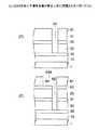
図1(A)〜図2(F)はSiO2膜を層間絶縁膜として用いた、従来のデュアルダマシン法による多層配線構造の形成工程を示す。
図1(A)の工程を参照するに、Si基板1上には図示を省略した絶縁膜を介してCu等の下層配線パターン10が形成されており、前記下層配線パターン10上にはSiNよりなる第1のエッチングストッパ膜12がプラズマCVD法により形成される。前記SiN膜12上にはさらにSiO2よりなる第1の層間絶縁膜14がプラズマCVD法により形成され、前記SiO2膜14上にはさらにSiNよりなる第2のエッチングストッパ膜16がプラズマCVD法により形成される。さらにその上にレジストパターン18が形成される。レジストパターン18中にはレジスト開口部18Aが、多層配線構造中に形成されるコンタクトホールに対応して形成される。
【0004】
次に図1(B)の工程で、前記レジストパターン18をマスクに前記SiN膜16に対してドライエッチングを行ない、前記レジスト開口部18Aに対応して開口部20を前記SiN膜16中に形成する。さらに、前記開口部20の形成の後、前記レジストパターン18をアッシングにより除去する。
次に、図1(C)の工程でSiN膜16上に前記開口部20を覆うようにSiO2膜22が第2の層間絶縁膜としてCVD法により形成される。
【0005】
さらに図2(D)の工程において、前記SiN膜16中の開口部20を含むように、前記SiO2膜22中に形成される配線溝に対応した開口部24Aを有するレジストパターン24が形成され、図2(E)の工程で前記レジスト膜24をマスクとしてSiO2膜22をドライエッチングすることにより、前記SiO2膜22中に配線溝26が形成される。前記配線溝26の底部には前記SiN膜16が露出されるが、ドライエッチング工程をさらに継続することにより、前記SiN膜16をマスクに前記SiO2膜14がドライエッチングされ、前記SiO2膜14中に前記開口部20に対応したコンタクトホール28が形成される。前記コンタクトホール28の底部にはSiN膜12が露出される。
【0006】
さらに図2(F)の工程において、前記コンタクトホール28の底に露出されたSiN膜12をエッチング・除去することにより、コンタクトホール28の底にCu配線パターン10が露出され、前記配線溝26及びコンタクトホール28をCuのリフローで埋めることにより多層配線構造の形成工程が完了する。
上記デュアルダマシン法による多層配線構造の形成工程では、一度のドライエッチング工程により、配線溝とコンタクトホールとが同時に形成されるため、半導体装置の製造工程が簡素化される。
【0007】
一方、上記従来の多層配線構造では、層間絶縁膜14あるいは22が誘電率の高いSiO2より形成されるため配線容量が大きくなることが避けられず、先に説明した配線遅延の問題を解消することができない。
これに対し、従来より層間絶縁膜として誘電率の低い有機層間絶縁膜を使った多層配線構造が提案されている。
【0008】
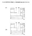
図3(A)〜(C)及び図4(D)〜(E)に示す工程は、かかる有機層間絶縁膜を使った多層配線構造の形成工程の一例を示す。ただし、図中先に説明した部分には同一の参照符号を付し、説明を省略する。
図3(A)を参照するに、前記基板1上のCu配線パターン10上には第1のエッチングストッパ膜としてSiN膜30がプラズマCVD法により形成されているが、この第2の従来の方法では、前記第1の層間絶縁膜として有機SOG膜32を前記SiN膜30上にスピンコーティング等により塗布・形成する。さらに、第2のエッチングストッパ膜としてSiN膜34を前記有機SOG膜32上にプラズマCVD法により形成し、さらに第2の層間絶縁膜として有機SOG膜36を、前記SiN膜34上にプラズマCVD法により形成する。
【0009】
さらに前記有機SOG膜36上に、前記有機SOG膜32中に形成されるコンタクトホールに対応した開口部38Aを有するレジストパターン38を形成する。
続いて図3(B)の工程で、前記レジストパターン38をマスクとして前記有機SOG膜36、SiN膜34および有機SOG膜32をエッチングし、コンタクトホール40を形成する。
【0010】
さらに図3(C)の工程で、前記有機SOG膜36上に前記コンタクトホール40を含むように、前記膜36中に形成される配線溝に対応した開口部42Aを有するレジストパターン42を形成する。
次に図4(D)の工程で、前記レジストパターン42をマスクとして前記有機SOG膜36をエッチングし、膜36中に配線溝44を形成する。前記配線溝44の形成の後、レジストパターン42をアッシングにより除去する。先にも説明したように配線溝44はコンタクトホール40を含み、底部において前記SiN膜34を露出する。
【0011】
さらに図4(E)の工程では、上記エッチング工程に続いて前記配線溝44底部のSiN膜34とコンタクトホール40底部のSiN膜30とをエッチングし、下層のCu配線パターン10を表出させる。
以上のように、第2の従来法によるデュアルダマシンプロセスでは、コンタクトホール形成と配線溝形成のエッチング工程を2度に分けて行うものであり、配線溝形成用のレジストパターニングの際に、マスク合わせが容易になる。
【0012】
前記図3(A)〜図4(E)の工程で使われた有機層間絶縁膜32および36は、先に説明した図1(A)〜図2(F)の層間絶縁膜形成工程に対しても適用可能である。また、先に説明した図1(A)〜図2(F)の工程で使われた無機層間絶縁膜を図3(A)〜図4(E)の層間絶縁膜形成工程について適用することも可能である。
【0013】
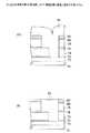
一方、上記従来の多層配線構造では、図5(A)に示すように、レジストパターン24を形成する際に位置ずれが生じると、前記SiN膜16中の開口部20がSiO2膜22中に形成される配線溝26中に全く、あるいは部分的に含まれない場合が生じる。
このような場合に図5(B)に示すようにレジストパターン24を修正せずにドライエッチングを行い、コンタクトホール28の開口を試みると、上記マスク合わせの位置ずれに対応して、コンタクトホール28の開口径が設計値よりも小さくなり、その結果コンタクトホールのアスペクト比が増大する。最悪の場合、コンタクトホール28は開口しないおそれがある。同様な問題が、図3(A)〜図4(E)に示す有機層間絶縁膜を使った多層配線構造においても生じる。
【0014】
【発明が解決しようとする課題】
かかるレジストパターンの位置ずれの問題は、層間絶縁膜22としてSiO2等の無機層間絶縁膜を使っている場合には、単に位置ずれを起こしたレジストパターン24を溶解・除去し、新たにレジストパターン24を形成し直すことで対応が可能である。
【0015】
しかしながら、前記層間絶縁膜22として有機物よりなる低誘電率材料を用いた場合には、以下に図6(A)〜図7(D)を参照して説明する問題が生じる。ただし、図6(A)〜図7(D)中、先に説明した部分には同一の参照符号を付し、説明を省略する。図6(A)中、有機SOG膜36上にはエッチングストッパ膜としてSiO2膜60が形成されている。
【0016】
図6(A)を参照するに、前記レジストパターン38が前記有機SOG膜36を覆う前記SiO2膜60上に形成され、図6(B)の工程で前記レジストパターン38をマスクに、前記SiO2膜60中に前記レジスト開口部38Aに対応した開口部60Aが形成される。さらに、図7(C)の工程において前記レジストパターン38を除去し、SOG膜36および32中に、間に介在するSiN膜34をも含めて前記開口部60Aに対応したコンタクトホール62を、前記開口部60Aを形成された前記SiO2膜をマスクに形成し、さらに図7(D)の工程において前記レジストパターン64を前記SiO2膜60上に形成する。
【0017】
図7(D)の工程では、レジストパターン64を、レジスト開口部64Aにおいてコンタクトホール62が露出するように形成する必要があるが、レジストパターン64形成の際にマスク合わせがずれると、レジストパターン64がコンタクトホール62を完全に、あるいは部分的に覆う場合がある。
このようなレジストパターン64の位置ずれが生じた場合には、レジストを再形成するために、レジストパターン64をアッシングにより除去する必要があるが、層間絶縁膜36として有機SOG膜を使った場合には、コンタクトホール62の側壁面において前記有機SOG膜36が露出しており、従って前記レジストパターン64をアッシングにより除去すると、同時に前記有機SOG膜36も酸化され侵食されてしまう。換言すると、従来の有機層間絶縁膜を使ったデュアルダマシン構造の多層配線構造では、レジストパターンの再生は一般に不可能である。レジストパターンの再生が不可能であるため、従来の有機層間絶縁膜を使った多層配線構造では歩留まりが低く、半導体装置の製造費用の増大が避けられない。
【0018】
そこで、本発明は上記従来の課題を解決した、新規で有用な半導体装置およびその製造方法を提供することを概括的課題とする。
本発明のより具体的な課題は、低誘電率の有機層間絶縁膜を用いたダマシン構造の多層配線構造の形成の際に、マスク位置ずれの補正を可能とし、半導体装置製造の際の歩留まりを向上できる半導体装置の製造方法を提供することにある。
【0019】
【課題を解決するための手段】
本発明は上記の課題を、
請求項1に記載したように、
基板上に第1の層間絶縁膜を形成する工程と、
前記第1の層間絶縁膜上に第2の層間絶縁膜を形成する工程と、
前記第2の層間絶縁膜上に第1のエッチングストッパ膜を形成する工程と、
前記第1のエッチングストッパ膜上に、前記第1のエッチングストッパ膜とは異なる第2のエッチングストッパ膜を形成する工程と、
前記第2のエッチングストッパ膜中に第1の開口部を、前記第1のエッチングストッパ膜が露出するように形成する工程と、
前記露出した第1のエッチングストッパ膜中に、第2の開口部を形成する工程と、
前記第1のエッチングストッパ膜をマスクとして、前記第2の層間絶縁膜をエッチングして前記第2の開口部に対応した第3の開口部を前記第2の層間絶縁膜中に形成する工程と、
前記第2のエッチングストッパ膜をマスクとして前記第2の層間絶縁膜をエッチングし、前記第2の層間絶縁膜中に前記第1の開口部に対応した配線溝を形成する工程と、
前記第1の層間絶縁膜中に、前記第3の開口部に対応したコンタクトホールを形成する工程と、
さらに前記コンタクトホールと前記配線溝とを導体によって埋める工程とを有し、
前記コンタクトホールと配線溝とを導体によって埋める工程は、
前記第2のエッチングストッパ膜上にCu層を、前記コンタクトホールと配線溝とを埋めるように堆積する工程と、
前記第2のエッチングストッパ膜上のCu層を、化学機械研磨による除去する工程とを含むことを特徴とする半導体装置の製造方法により、または
請求項2に記載したように、
基板上に第1の層間絶縁膜を形成する工程と、
前記第1の層間絶縁膜上に、第2の層間絶縁膜を形成する工程と、
前記第2の層間絶縁膜上に、第1のエッチングストッパ膜となるSiC膜を形成する工程と、
前記SiC膜上に、前記第1のエッチングストッパ膜とは異なる第2のエッチングストッパ膜を形成する工程と、
前記第2のエッチングストッパ膜をエッチングして、前記SiC膜が露出する第1の開口部を形成する工程と、
前記SiC膜をエッチングして、露出した前記SiC膜に、第2の開口部を形成する工程と、
前記第2の層間絶縁膜をエッチングして、前記第2の開口部に対応した第3の開口部を形成する工程と、
前記第2のエッチングストッパ膜をマスクとして前記第2の層間絶縁膜をエッチングし、前記第2の層間絶縁膜中に前記第1の開口部に対応した配線溝を形成する工程と、
前記第1の層間絶縁膜中に、前記第3の開口部に対応したコンタクトホールを形成する工程と、
前記コンタクトホールと前記配線溝とを導体によって埋める工程とを有することを特徴とする半導体装置の製造方法により、または
請求項3に記載したように、
前記第2の開口部を形成する工程は、前記第1のエッチングストッパ膜上に、前記第2の開口部に対応するレジスト開口部を有するレジストパターンを形成する工程と、前記レジストパターンをマスクに前記第1のエッチングストッパ膜をパターニングする工程とを含むことを特徴とする請求項1または2記載の半導体装置の製造方法により、または
請求項4に記載したように、
さらに、前記レジストパターンを形成する工程の後、前記第1のエッチングストッパ膜をパターニングする工程の前に、前記レジストパターンを除去し、新たに前記第2の開口部に対応するレジスト開口部を有するレジストパターンを形成する工程を含み、前記第1のエッチングストッパ膜をパターニングする工程は、前記新たに形成されたレジストパターンをマスクに実行されることを特徴とする請求項3記載の半導体装置の製造方法により、または
請求項5に記載したように、
前記配線溝を形成する工程と前記コンタクトホールを形成する工程とは同時に実行されることを特徴とする請求項1〜4のうち、いずれか一項記載の半導体装置の製造方法により、または
請求項6に記載したように、
前記第1のエッチングストッパ膜としてSiN膜を用いることを特徴とする請求項1,3〜5のうち、いずれか一項記載の半導体装置の製造方法により、または
請求項7に記載したように、
前記第2のエッチングストッパ膜としてSiO2膜を用いることを特徴とする請求項1,3〜6のうち、いずれか一項記載の半導体装置の製造方法により、または
請求項8に記載したように、
前記第1のエッチングストッパ膜としてSiO2膜を用い、かつ前記第2のエッチングストッパ膜としてTiN膜を用いることを特徴とする請求項1,3〜5のうち、いずれか一項記載の半導体装置の製造方法により、または
請求項9に記載したように
前記第1のエッチングストッパ膜として、SiC膜とSiO2膜との積層膜を使うことを特徴とする請求項1,3〜5のうち、いずれか一項記載の半導体装置の製造方法により、または
請求項10に記載したように、
前記第1のエッチングストッパ膜および前記第2のエッチングストッパ膜として、SiC膜とSiO2膜とSiN膜とからなる多層膜を使うことを特徴とする請求項1〜5のうち、いずれか一項記載の半導体装置の製造方法により、または
請求項11に記載したように、
前記第1の層間絶縁膜と前記第2の層間絶縁膜との間隙に絶縁膜を形成する工程を含むことを特徴とする請求項1〜10のうち、いずれか一項記載の半導体装置の製造方法により、または
請求項12に記載したように、
前記絶縁膜として、SiC膜を使うことを特徴とする請求項11記載の半導体装置の製造方法により、または
請求項13に記載したように、
前記第2の層間絶縁膜は、有機絶縁膜であることを特徴とする請求項1〜12のうち、いずれか一項記載の半導体装置の製造方法により、または
請求項14に記載したように、
前記第1の層間絶縁膜は、有機絶縁膜であることを特徴とする請求項1〜13のうち、いずれか一項記載の半導体装置の製造方法により、または
請求項15に記載したように、
前記コンタクトホールと配線溝とを導体により埋める工程は、前記第2のエッチングストッパ膜上にCu層を、前記コンタクトホールと配線溝とを埋めるように堆積する工程と、前記第2のエッチングストッパ膜上のCu層を化学機械研磨により除去する工程とを含むことを特徴とする請求項2記載の半導体装置の製造方法により、または
請求項16に記載したように、
基板上に、第1の層間絶縁膜を形成する工程と、
前記第1の層間絶縁膜上に、第2の層間絶縁膜を形成する工程と、
前記第2の層間絶縁膜上に、第3の層間絶縁膜となる有機絶縁膜を形成する工程と、
前記第3の層間絶縁膜上に、第1のエッチングストッパ膜となるSiC膜を形成する工程と、
前記SiC膜上に、前記第1のエッチングストッパ膜とは異なる第2のエッチングストッパ膜を形成する工程と、
前記第2のエッチングストッパ膜をエッチングして、前記SiC膜が露出する第1の開口部を形成する工程と、
前記SiC膜をエッチングして、露出した前記SiC膜に、第2の開口部を形成する工程と、
前記第3の層間絶縁膜をエッチングして、前記第2の開口部に対応した第3の開口部を形成する工程と、
前記第2のエッチングストッパ膜をマスクとして、露出した前記SiC膜および前記第3の層間絶縁膜をエッチングし、前記第3の層間絶縁膜中に、前記第1の開口部に対応した配線溝を形成する工程と、
前記第2の層間絶縁膜および前記第1の層間絶縁膜をエッチングして、前記第3の開口部に対応したコンタクトホールを形成する工程と、
前記コンタクトホールと前記配線溝とを導体により埋める工程とを有することを特徴とする半導体装置の製造方法により、または
請求項17に記載したように、
基板上に、第1の層間絶縁膜となる第1の有機絶縁膜を形成する工程と、
前記第1の層間絶縁膜上に、第2の層間絶縁膜となる第1のSiC膜を形成する工程と、
前記第2の層間絶縁膜上に、第3の層間絶縁膜となる第2の有機絶縁膜を形成する工程と、
前記第2の有機絶縁膜上に、第1のエッチングストッパ膜となる第2のSiC膜を形成する工程と、
前記第2のSiC膜上に、前記第1のエッチングストッパ膜とは異なる第2のエッチングストッパ膜を形成する工程と、
前記第2のエッチングストッパ膜をエッチングして、前記SiC膜が露出する第1の開口部を形成する工程と、
前記SiC膜をエッチングして、露出した前記SiC膜に、第2の開口部を形成する工程と、
前記第2の有機絶縁膜をエッチングして、前記第2の有機絶縁膜中に、前記第2の開口部に対応した第3の開口部を形成する工程と、
前記第2のエッチングストッパ膜をマスクとして、露出した前記SiC膜および前記第2の有機絶縁膜をエッチングして、前記第2の有機絶縁膜中に、前記第1の開口部に対応した配線溝を形成する工程と、
前記第1のSiC膜および前記第1の有機絶縁膜をエッチングして、前記第3の開口部に対応したコンタクトホールを形成する工程と、
前記コンタクトホールと前記配線溝とを導体によって埋める工程とを有することを特徴とする半導体装置の製造方法により、または
請求項18に記載したように、
基板と、
前記基板上に形成された第1の層間絶縁膜と、
前記第1の層間絶縁膜上に形成された第2の層間絶縁膜と、
前記第1の層間絶縁膜に形成されたコンタクトホールと、
前記第2の層間絶縁膜に前記コンタクトホールと連続して形成された配線溝と、
前記コンタクトホールと前記配線溝とを埋める導体とよりなる半導体装置であって、
前記第2の層間絶縁膜上に形成された第1のエッチングストッパ膜と、
前記第1のエッチングストッパ膜上に形成された、前記第1のエッチングストッパ膜とは異なる第2のエッチングストッパ膜とをさらに有し、
前記第1のエッチングストッパ膜および前記第2のエッチングストッパ膜に、前記配線溝に連続して形成され、前記配線溝に対応した第1の開口部をさらに有し、
前記第1の開口部は、前記導体により埋め込まれたことを特徴とする半導体装置により、または
請求項19に記載したように、
前記導体は、デュアルダマシン配線を形成することを特徴とする請求項18記載の半導体装置により、または
請求項20に記載したように、
前記導体はCuよりなることを特徴とする請求項18または19記載の半導体装置により、または
請求項21に記載したように、
前記第2のエッチングストッパ膜の表面と前記導体の表面とは同一平面を形成することを特徴とする請求項18記載の半導体装置により、または
請求項22に記載したように、
前記第1の層間絶縁膜と前記第2の層間絶縁膜との間に形成された絶縁膜を有することを特徴とする請求項18〜21のうち、いずれか一項記載の半導体装置により、または
請求項23に記載したように、
前記絶縁膜は、SiC膜であることを特徴とする請求項22記載の半導体装置により、または
請求項24に記載したように、
前記絶縁膜に、前記コンタクトホールおよび前記配線溝に連続して形成され、前記コンタクトホールに対応した第2の開口部をさらに有し、前記第2の開口部は前記導体によって埋め込まれたことを特徴とする請求項22または23記載の半導体装置により、または
請求項25に記載したように、
前記第2の層間絶縁膜は、有機絶縁膜であることを特徴とする請求項18〜24のうち、いずれか一項記載の半導体装置により、または
請求項26に記載したように、
前記第1の層間絶縁膜は、有機絶縁膜であることを特徴とする請求項18〜25のうち、いずれか一項記載の半導体装置により、解決する。
【0020】
[作用]
本発明によれば、前記第2の有機層間絶縁膜を、エッチング特性の異なる第1および第2のエッチングストッパ膜で覆い、前記第2のエッチングストッパ膜を配線溝パターンに対応してパターニングし、その下の第1のエッチングストッパ膜を、レジストプロセスにより、前記配線溝中に形成されるコンタクトホールに対応してパターニングし、前記第1のエッチングストッパ膜および第2のエッチングストッパ膜をハードマスクとして使って前記第1および2の層間絶縁膜中にコンタクトホールと配線溝とをデュアルダマシン法により形成する際に、前記第1のエッチングストッパ膜をパターニングするのに使われるレジストパターンに不良があった場合にも、有機物よりなる前記第2の層間絶縁膜が前記第1のエッチングストッパ膜で完全に覆われているため前記不良レジストパターンを問題なく除去でき、新たなレジストパターンを形成することができる。このため、半導体装置の製造歩留まりが大きく向上する。
【0021】
【発明の実施の形態】
[第1の実施例]
次に本発明の第1実施例による半導体装置の製造工程を、図8(A)〜図11(I)を参照しながら説明する。
図8(A)を参照するに、基板70上には図示しなう絶縁膜を介してCuよりなる第1層配線パターン71が形成されており、前記配線層71上には、バリア膜72としてSiN膜がプラズマCVD法により約30nmの厚さに形成される。
【0022】
次に、前記バリア膜72上に、第1の層間絶縁膜74として有機SOG膜74をスピンコーティング法により約700nmの厚さに塗布・形成し、さらに前記第1の層間絶縁膜74上に絶縁膜76としてSiO2膜をプラズマCVD法により約20nmの厚さに形成する。絶縁膜76はSiN膜、SiON膜あるいはSiC膜であってもよい。
【0023】
さらに、第2の層間絶縁膜78として有機SOG膜を前記絶縁膜76上に、スピンコーティング法により約400nmの厚さに形成し、次に前記第2の層間絶縁膜78上に2層構造のエッチングストッパ膜81を形成する。より具体的には、前記エッチングストッパ膜81は前記第2の層間絶縁膜78上に形成された厚さが約20nmのSiNよりなる第1層のエッチングストッパ膜80と、前記第1層のエッチングストッパ膜80上に形成された厚さが約100nmのSiO2よりなる第2層のエッチングストッパ膜82とよりなる。前記SiN膜80と前記SiO2膜82とは、共にプラズマCVD法により形成される。
【0024】
さらに、前記エッチングストッパ膜82の形成の後、前記エッチングストッパ膜82上に、前記有機SOG膜78中に形成したい配線溝に対応した開口部84Aを有するレジストパターン84を形成する。
ここで、前記エッチングストッパ膜80,82としては、以下のような組み合わせも可能である。
【0025】
即ち、前記エッチングストッパ膜80にSiON膜を用い、前記エッチングストッパ膜82にSiO2膜を用いてもよい。また前記エッチングストッパ膜80にSiO2膜、SiON膜、SiN膜あるいはSiC膜を用い、前記エッチングストッパ膜82にアモルファスSi膜を用いてもよい。またさらに前記エッチングストッパ膜80にSiO2膜、SiN膜あるいはSiC膜を用い、かつ前記エッチングストッパ膜82にTiN膜を用いてもよい。さらに、前記各例において、前記エッチングストッパ膜80としてSiO2膜とSiC膜とよりなるスタック構造を用いることもできる。前記エッチングストッパ膜80および82は、典型的にはプラズマCVD法により形成されるが、他の成膜方法を使用することもできる。
【0026】
次に、図8(B)の工程において、前記レジストパターン84をマスクとして前記エッチングストッパ膜82を例えばCF4/ Ar系のドライエッチング法によりパターニングし、その後で前記レジストパターン84をアッシングにより除去する。エッチングストッパ膜82のパターニングにより、膜82中には前記レジストパターン開口部84Aに対応した開口部82Aが形成される。前記開口部82Aにおいて前記エッチングストッパ膜80が露出される。
【0027】
図8(B)の工程では、さらに前記レジストパターン84の除去に続いて前記エッチングストッパ膜82、および前記開口部82Aで露出されたエッチングストッパ膜80上に、前記有機SOG膜74中に形成されるコンタクトホールに対応した開口部86Aを有するレジストパターン86を、前記開口部86Aが前記開口部82A中に形成されるように形成する。
【0028】
ところで、上記レジストパターン86を形成する際には、前記開口部86Aを開口部82A中に形成する必要があるため、露光時のマスク合わせを数μm以下の精度をもって行う必要がある。しかしこのような高精度でのマスク合わせは困難であり、レジスト開口部86Aの位置が開口部82Aの外側に形成されることもある。このような状態を図8(C)に示す。
【0029】
図8(C)に示すようにレジスト開口部86Aの位置がずれ、レジスト開口部82Aの外側に形成された場合には、レジストパターン86の形成をやり直すことが必要である。この場合は、上記レジストパターン86をアッシング等により一旦除去し、再度レジストパターン86を所定の位置に形成する。
かかるレジストパターン86の再生工程の際に、本実施例によれば前記有機SOG膜78がエッチングストッパ膜80によって覆われているため、不良レジストパターン86をアッシング等により除去しても、従来問題であったような、かかるアッシング時に前記有機SOG膜78あるいは74の一部も同時に除去されてしまう問題を回避することができる。
【0030】
次に図9(D)の工程で、図8(B)中のレジストパターン86をマスクとして、その下層のエッチングストッパ膜80をパターニングし、続いてその下の有機SOG膜78をO2/ N2系のドライエッチングにより、前記エッチングストッパ膜80および82をマスクにパターニングし、開口部93を形成する。前記開口部93の形成の後、前記レジストパターン86をアッシング等により除去する。
【0031】
さらに図9(E)の工程で、前記エッチングストッパ膜82をマスクとして、その下層に表出したエッチングストッパ膜80をCF4/ Ar系のドライエッチング法により除去する。この際工程においては、前記有機SOG膜78中の開口部93の底部に表出したSiN膜76も同時に除去される。この時に、最上部のエッチングストッパ膜82はエッチング除去されないような厚さに設定することが必要であり、例えば100nm程度の膜厚に設定する。
【0032】
次に図10(F)の工程で、残留しているエッチングストッパ膜82をマスクにO2/ N2系のドライエッチングを行なうことにより、第2の有機層間絶縁膜78および有機SOG膜74をパターニングし、配線溝91及びコンタクトホール89を同時に開口する。その際、配線溝91の底部に露出される前記SiO2膜76はコンタクトホール89を形成する際のマスクとして作用する。
【0033】
さらに、図10(G)の工程で、前記コンタクトホール89の底部に表出したバリア膜72をCF4/ Ar系のドライエッチング法により除去した後、図11(H)の工程において図10(G)の構造上に前記コンタクトホール89および配線溝91を埋めるようにCu層83をCVD法により堆積し、さらに図11(I)の工程において前記Cu層83をリフローさせた後、CMP法により前記エッチングストッパ膜82上のCu層83を除去し、前記コンタクトホール89および配線溝91を埋めるCu配線パターンを形成する。
【0034】
本実施例によれば、前記有機SOG膜78,SiN膜76および有機SOG膜74からなる層間絶縁膜中にいわゆるデュアルダマシン法によりコンタクトホール及び配線溝部を形成する際に、前記有機SOG膜78をエッチングストッパ膜80,82により覆うことにより、万が一レジストパターン86を再生する必要が生じた場合でも、前記有機SOG膜78を侵食することなく、不良レジストパターン86を除去することが可能となり、半導体装置製造の際の歩留まりが大きく向上する。
【0035】
なお、本実施例において前記下側層間絶縁膜74としては、有機SOG膜以外にF添加SiO2膜等の低誘電率無機層間絶縁膜を使うこともできる。
また前記2層エッチングストッパ膜81に代えて、SiO2膜、SiN膜あるいはSiC膜を3層以上積層した多層積層構造膜を用いてもよい。
図11(H)の工程において、前記Cu層83の堆積はCVD法以外にも、電解めっき法によっても可能である。この場合には、先に薄いCu膜をスパッタリングにより、前記コンタクトホール89および配線溝91の内面を覆うように形成し、このようにして形成されたCu膜を電極に、電解液中において前記Cu膜上に前記Cu層83を成長させる。
【0036】
[第2の実施例]
次に本発明の第2実施例による半導体装置の製造方法を、図12(A),(B)を参照しながら説明する。ただし、図12(A),(B)中、先に説明した部分には同一の参照符号を付し、説明を省略する。
図12(A)を参照するに、この工程は前記図8(B)の工程に対応するが、レジストパターン86の形成の際に、わざとマスク位置を開口部82Aに対してずらしている。
【0037】
即ち、図12(A)の工程では、レジストパターン86は、パターン開口部86Aが前記エッチングストッパ膜82中の開口部82Aのエッジを含むように形成されており、その結果図12(B)のエッチング工程を行なった場合、形成されるコンタクトホール89の大きさは、レジスト開口部86Aの大きさよりも小さくなる。
【0038】
このように、レジストパターン86をわざとずらして微細なコンタクトホールを形成する工程は、図5(A),(B)でも説明したようにレジストパターン86のわずかな位置誤差により解像しなくなる危険があるが、本発明による方法では、このような場合に不良レジストパターン86を問題なく除去し、新たにレジストパターン86を再形成できるので、不良率が増大する問題を回避することができる。
【0039】
以上の各実施例においては、前記層間絶縁膜74,78として有機SOG膜を使ったが、前記有機SOG膜の代わりに例えば以下の化学式1
【0040】
【化1】
で表されるアモルファスフルオロカーボン膜を使うことも可能である。かかるアモルファスフルオロカーボン膜は誘電率が典型的には2.4〜2.7の値を有し、CVD法により形成することができる。
以上、本発明を好ましい実施例について説明したが、本発明はかかる特定の実施例に限定されるものではなく、特許請求の範囲に記載した要旨内において様々な変形・変更が可能である。
【0042】
【発明の効果】
上述の如く本発明によれば、次に述べる効果を奏することができる。
請求項1乃至26記載の発明により、デュアルダマシン法を使った多層配線形成工程において層間絶縁膜として低誘電率有機層間絶縁膜を使用することにより配線遅延の問題を抑制できると同時に、前記有機層間絶縁膜を第1および第2のエッチングストッパ膜で覆うことにより不良レジストパターンの再生が可能になる。その結果、本発明では配線遅延の少ない高速動作半導体装置を高い歩留まりで製造できる。
【図面の簡単な説明】
【図1】(A) 〜(C) は従来半導体装置の製造工程を示す図(その1)である。
【図2】(D)〜(F)は従来の半導体装置の製造工程を示す図(その2)である。
【図3】(A)〜(C)は別の従来の半導体装置の製造工程を示す図(その1)である。
【図4】(D)〜(E)は別の従来の半導体装置の製造工程を示す図(その2)である。
【図5】従来の半導体装置の製造工程の問題点を説明する図である。
【図6】(A),(B)は従来の半導体装置の製造工程の問題点を示す図(その1)である。
【図7】(C),(D)は従来の半導体装置の製造工程の問題点を示す図(その2)である。
【図8】(A)〜(C)は本発明の第1実施例による半導体装置の製造工程を示す図(その1)である。
【図9】(D),(E)は本発明の第1実施例による半導体装置の製造工程を示す図(その2)である。
【図10】(F),(G)は本発明の第1の実施例による半導体装置の製造工程を示す図(その3)である。
【図11】(H),(I)は本発明の第1の実施例による半導体装置の製造工程を示す図(その4)である。
【図12】(A),(B)は本発明の第2実施例による半導体装置の製造工程を示す図である。
【符号の説明】
1,70 基板
10 配線パターン
12,16,30,34 SiN膜
14,22 SiO2層間絶縁膜
18,24,38,42,64,84,86 レジストパターン
18A,24A,38A,42A,64A,84A,86A レジスト開口部
20,60A,82A ハードマスク開口部
26,44,91 配線溝
28,40,62,89,93 コンタクトホール
32,36、74,78 有機層間絶縁膜
71 第1層配線パターン
72 バリア膜
76 絶縁膜
80,81,82 エッチングストッパ−膜[0001]
BACKGROUND OF THE INVENTION
The present invention relates to a semiconductor device and a manufacturing method thereof, and more particularly to a semiconductor device having a multilayer wiring structure and a manufacturing method thereof.
With the progress of miniaturization technology, the integration density of semiconductor integrated circuits has been improved year by year. However, with the increase of such integration density, the problem of wiring delay due to wiring resistance and wiring capacitance in the semiconductor integrated circuit has become obvious. ing. In view of the problem of such wiring delay, recently, a technique for using low resistance Cu as a wiring pattern and using an organic film having a low dielectric constant as an interlayer insulating film has been studied.
[0002]
Conventionally, an effective method for patterning Cu by dry etching has not been known. Therefore, when Cu is used for a wiring pattern, a wiring groove and a contact hole are first formed in the interlayer insulating film, and this is filled with Cu. The so-called dual damascene method is used. In the dual damascene method, contact holes and wiring grooves are filled with a wiring material such as Cu, and unnecessary portions of the wiring material are polished and removed by a chemical mechanical polishing (CMP) method to form contact holes and wiring grooves. An embedded, flattened wiring pattern is formed. According to the dual damascene method, it is not necessary to form a narrow high-aspect-ratio wiring pattern by etching, and it is not necessary to embed a fine space between wirings with an interlayer insulating film. Can be easily formed. The formation of the multilayer wiring structure by the dual damascene method is more effective as the wiring aspect ratio increases and the total number of wirings increases, and greatly contributes to the reduction of the manufacturing cost of the ultrafine semiconductor device.
[0003]
[Prior art]
FIGS. 1A to 2F show SiO.2The formation process of the multilayer wiring structure by the conventional dual damascene method using a film | membrane as an interlayer insulation film is shown.
Referring to the process of FIG. 1A, a lower
[0004]
Next, in the step of FIG. 1B, dry etching is performed on the
Next, in the step of FIG. 1C, SiO 2 is covered on the SiN
[0005]
Further, in the step of FIG. 2D, the SiON so as to include the opening 20 in the SiN film 16.2A
[0006]
Further, in the step of FIG. 2F, by etching and removing the
In the formation process of the multilayer wiring structure by the dual damascene method, the wiring groove and the contact hole are simultaneously formed by one dry etching process, so that the manufacturing process of the semiconductor device is simplified.
[0007]
On the other hand, in the conventional multilayer wiring structure, the
On the other hand, a multilayer wiring structure using an organic interlayer insulating film having a low dielectric constant as an interlayer insulating film has been proposed.
[0008]
The steps shown in FIGS. 3A to 3C and FIGS. 4D to 4E show an example of a process for forming a multilayer wiring structure using such an organic interlayer insulating film. However, the same reference numerals are given to the portions described above in the drawing, and the description will be omitted.
Referring to FIG. 3A, a
[0009]
Further, a
3B, the
[0010]
3C, a
Next, in the step of FIG. 4D, the
[0011]
4E, the
As described above, in the dual damascene process according to the second conventional method, the etching process for forming the contact hole and the wiring groove is performed in two steps, and the mask alignment is performed at the time of resist patterning for forming the wiring groove. Becomes easier.
[0012]
The organic
[0013]
On the other hand, in the conventional multilayer wiring structure, as shown in FIG. 5A, when the resist
In such a case, when dry etching is performed without correcting the resist
[0014]
[Problems to be solved by the invention]
The problem of such misalignment of the resist pattern is that the
[0015]
However, when a low dielectric constant material made of an organic material is used as the
[0016]
Referring to FIG. 6A, the resist
[0017]
7D, it is necessary to form the resist
When such a misregistration of the resist
[0018]
SUMMARY OF THE INVENTION Accordingly, it is a general object of the present invention to provide a new and useful semiconductor device and a method for manufacturing the same that solve the above-described conventional problems.
A more specific problem of the present invention is that it enables correction of mask misalignment in the formation of a damascene multilayer wiring structure using an organic interlayer insulating film having a low dielectric constant, and improves the yield in manufacturing a semiconductor device. An object of the present invention is to provide a method for manufacturing a semiconductor device that can be improved.
[0019]
[Means for Solving the Problems]
The present invention solves the above problems.
As described in
Forming a first interlayer insulating film on the substrate;
Forming a second interlayer insulating film on the first interlayer insulating film;
Forming a first etching stopper film on the second interlayer insulating film;
Forming a second etching stopper film different from the first etching stopper film on the first etching stopper film;
Forming a first opening in the second etching stopper film such that the first etching stopper film is exposed;
Forming a second opening in the exposed first etching stopper film;
Etching the second interlayer insulating film using the first etching stopper film as a mask to form a third opening corresponding to the second opening in the second interlayer insulating film; ,
Etching the second interlayer insulating film using the second etching stopper film as a mask to form a wiring groove corresponding to the first opening in the second interlayer insulating film;
Forming a contact hole corresponding to the third opening in the first interlayer insulating film;
A step of filling the contact hole and the wiring groove with a conductor;
The step of filling the contact hole and the wiring groove with a conductor,
Depositing a Cu layer on the second etching stopper film so as to fill the contact hole and the wiring groove;
Or a step of removing the Cu layer on the second etching stopper film by chemical mechanical polishing, or
As described in claim 2,
Forming a first interlayer insulating film on the substrate;
Forming a second interlayer insulating film on the first interlayer insulating film;
Forming a SiC film serving as a first etching stopper film on the second interlayer insulating film;
Forming a second etching stopper film different from the first etching stopper film on the SiC film;
Etching the second etching stopper film to form a first opening from which the SiC film is exposed;
Etching the SiC film to form a second opening in the exposed SiC film;
Etching the second interlayer insulating film to form a third opening corresponding to the second opening;
Etching the second interlayer insulating film using the second etching stopper film as a mask to form a wiring groove corresponding to the first opening in the second interlayer insulating film;
Forming a contact hole corresponding to the third opening in the first interlayer insulating film;
A step of filling the contact hole and the wiring groove with a conductor, or a method of manufacturing a semiconductor device, or
As described in claim 3,
The step of forming the second opening includes forming a resist pattern having a resist opening corresponding to the second opening on the first etching stopper film, and using the resist pattern as a mask. 3. The method of manufacturing a semiconductor device according to
As described in claim 4,
Further, after the step of forming the resist pattern and before the step of patterning the first etching stopper film, the resist pattern is removed and a resist opening corresponding to the second opening is newly provided. 4. The method of manufacturing a semiconductor device according to claim 3, wherein the step of patterning the first etching stopper film includes a step of forming a resist pattern, and the step of patterning the first etching stopper film is performed using the newly formed resist pattern as a mask. By method or
As described in claim 5,
5. The method of manufacturing a semiconductor device according to
As described in claim 6,
6. The method of manufacturing a semiconductor device according to
As described in claim 7,
SiO as the second etching stopper film2A method of manufacturing a semiconductor device according to any one of
As described in claim 8,
SiO as the first etching stopper film2A method of manufacturing a semiconductor device according to any one of
As described in claim 9
As the first etching stopper film, an SiC film and SiO2A method of manufacturing a semiconductor device according to any one of
As described in
6. The multilayer film comprising a SiC film, a SiO2 film and a SiN film is used as the first etching stopper film and the second etching stopper film, respectively. Or a semiconductor device manufacturing method of
As described in claim 11,
11. The method of manufacturing a semiconductor device according to
As described in
The semiconductor device manufacturing method according to claim 11, wherein a SiC film is used as the insulating film, or
As described in claim 13,
The method of manufacturing a semiconductor device according to
As described in
The method of manufacturing a semiconductor device according to
As described in claim 15,
The step of filling the contact hole and the wiring groove with a conductor includes depositing a Cu layer on the second etching stopper film so as to fill the contact hole and the wiring groove, and the second etching stopper film. Or removing the upper Cu layer by chemical mechanical polishing, or by the method for manufacturing a semiconductor device according to claim 2,
As described in
Forming a first interlayer insulating film on the substrate;
Forming a second interlayer insulating film on the first interlayer insulating film;
Forming an organic insulating film to be a third interlayer insulating film on the second interlayer insulating film;
Forming a SiC film serving as a first etching stopper film on the third interlayer insulating film;
Forming a second etching stopper film different from the first etching stopper film on the SiC film;
Etching the second etching stopper film to form a first opening from which the SiC film is exposed;
Etching the SiC film to form a second opening in the exposed SiC film;
Etching the third interlayer insulating film to form a third opening corresponding to the second opening;
Using the second etching stopper film as a mask, the exposed SiC film and the third interlayer insulating film are etched, and a wiring groove corresponding to the first opening is formed in the third interlayer insulating film. Forming, and
Etching the second interlayer insulating film and the first interlayer insulating film to form a contact hole corresponding to the third opening;
A step of filling the contact hole and the wiring groove with a conductor, or a method for manufacturing a semiconductor device, or
As described in claim 17,
Forming a first organic insulating film to be a first interlayer insulating film on the substrate;
Forming a first SiC film to be a second interlayer insulating film on the first interlayer insulating film;
Forming a second organic insulating film to be a third interlayer insulating film on the second interlayer insulating film;
Forming a second SiC film serving as a first etching stopper film on the second organic insulating film;
Forming a second etching stopper film different from the first etching stopper film on the second SiC film;
Etching the second etching stopper film to form a first opening from which the SiC film is exposed;
Etching the SiC film to form a second opening in the exposed SiC film;
Etching the second organic insulating film to form a third opening corresponding to the second opening in the second organic insulating film;
Using the second etching stopper film as a mask, the exposed SiC film and the second organic insulating film are etched to form a wiring groove corresponding to the first opening in the second organic insulating film. Forming a step;
Etching the first SiC film and the first organic insulating film to form a contact hole corresponding to the third opening;
A step of filling the contact hole and the wiring groove with a conductor, or a method of manufacturing a semiconductor device, or
As described in claim 18,
A substrate,
A first interlayer insulating film formed on the substrate;
A second interlayer insulating film formed on the first interlayer insulating film;
A contact hole formed in the first interlayer insulating film;
A wiring groove formed continuously with the contact hole in the second interlayer insulating film;
A semiconductor device comprising a conductor filling the contact hole and the wiring groove;
A first etching stopper film formed on the second interlayer insulating film;
And a second etching stopper film different from the first etching stopper film formed on the first etching stopper film.And
The first etching stopper film and the second etching stopper film are formed continuously with the wiring groove, and further have a first opening corresponding to the wiring groove,
The first opening is embedded by the conductorOr by a semiconductor device characterized by
As described in claim 19,
The semiconductor device according to claim 18, wherein the conductor forms a dual damascene wiring, or
As described in
20. The semiconductor device according to claim 18 or 19, wherein the conductor is made of Cu.Is
ContractClaim21As described in
The surface of the second etching stopper film and the surface of the conductor form the same plane.18By the described semiconductor device or
Claim22As described in
19. An insulating film formed between the first interlayer insulating film and the second interlayer insulating film.21Or a semiconductor device according to any one of
Claim23As described in
The insulating film is a SiC film.22By the described semiconductor device or
Claim24As described in
The insulating film is formed continuously with the contact hole and the wiring groove, and further includes a second opening corresponding to the contact hole, and the second opening is embedded by the conductor. Characteristic claims22Or23By the described semiconductor device or
Claim25As described in
The second interlayer insulating film is an organic insulating film.24Or a semiconductor device according to any one of
Claim26As described in
19. The first interlayer insulating film is an organic insulating film.25The problem is solved by the semiconductor device according to any one of the above.
[0020]
[Action]
According to the present invention, the second organic interlayer insulating film is covered with first and second etching stopper films having different etching characteristics, and the second etching stopper film is patterned corresponding to a wiring groove pattern, The first etching stopper film therebelow is patterned by a resist process corresponding to the contact hole formed in the wiring trench, and the first etching stopper film and the second etching stopper film are used as a hard mask. When a contact hole and a wiring groove are formed in the first and second interlayer insulating films by a dual damascene method, there is a defect in a resist pattern used for patterning the first etching stopper film. Also in this case, the second interlayer insulating film made of an organic material is completed by the first etching stopper film. The defective because it is covered with the resist pattern can be removed without any problem, it is possible to form a new resist pattern. For this reason, the manufacturing yield of the semiconductor device is greatly improved.
[0021]
DETAILED DESCRIPTION OF THE INVENTION
[First embodiment]
Next, a manufacturing process of the semiconductor device according to the first embodiment of the present invention will be described with reference to FIGS. 8 (A) to 11 (I).
Referring to FIG. 8A, a first
[0022]
Next, an
[0023]
Further, an organic SOG film is formed as a second
[0024]
Further, after the formation of the
Here, the
[0025]
That is, a SiON film is used as the
[0026]
Next, in the step of FIG. 8B, the
[0027]
In the step of FIG. 8B, the
[0028]
By the way, when the resist
[0029]
As shown in FIG. 8C, when the position of the resist
According to this embodiment, the
[0030]
Next, in the step of FIG. 9D, using the resist
[0031]
Further, in the step of FIG. 9E, the
[0032]
Next, in the step shown in FIG. 10F, the remaining
[0033]
Further, in the step of FIG. 10G, the
[0034]
According to the present embodiment, when the contact hole and the wiring groove are formed by the so-called dual damascene method in the interlayer insulating film composed of the
[0035]
In this embodiment, as the lower
In place of the two-layer
In the step of FIG. 11 (H), the
[0036]
[Second Embodiment]
Next, a semiconductor device manufacturing method according to the second embodiment of the present invention will be described with reference to FIGS. However, in FIGS. 12A and 12B, the same reference numerals are given to the portions described above, and description thereof is omitted.
Referring to FIG. 12A, this step corresponds to the step of FIG. 8B, but the mask position is intentionally shifted with respect to the
[0037]
That is, in the process of FIG. 12A, the resist
[0038]
In this manner, the step of forming the fine contact hole by intentionally shifting the resist
[0039]
In each of the above embodiments, an organic SOG film is used as the
[0040]
[Chemical 1]
It is also possible to use an amorphous fluorocarbon film represented by Such an amorphous fluorocarbon film typically has a dielectric constant of 2.4 to 2.7 and can be formed by a CVD method.
Although the present invention has been described with reference to the preferred embodiments, the present invention is not limited to such specific embodiments, and various modifications and changes can be made within the scope described in the claims.
[0042]
【The invention's effect】
As described above, according to the present invention, the following effects can be obtained.
[Brief description of the drawings]
FIGS. 1A to 1C are views (No. 1) showing a manufacturing process of a conventional semiconductor device. FIGS.
FIGS. 2D to 2F are views (No. 2) showing a manufacturing process of a conventional semiconductor device. FIGS.
FIGS. 3A to 3C are views (No. 1) illustrating another conventional manufacturing process of a semiconductor device. FIGS.
FIGS. 4D to 4E are views (No. 2) showing another conventional semiconductor device manufacturing process; FIGS.
FIG. 5 is a diagram for explaining a problem in a manufacturing process of a conventional semiconductor device.
FIGS. 6A and 6B are views (No. 1) illustrating problems in the manufacturing process of a conventional semiconductor device. FIGS.
FIGS. 7C and 7D are diagrams (part 2) illustrating problems in the manufacturing process of the conventional semiconductor device. FIGS.
FIGS. 8A to 8C are views (No. 1) showing a manufacturing process of a semiconductor device according to the first embodiment of the invention; FIGS.
FIGS. 9D and 9E are views (No. 2) showing a manufacturing step of the semiconductor device according to the first embodiment of the invention; FIGS.
FIGS. 10F and 10G are views (No. 3) showing the manufacturing steps of the semiconductor device according to the first example of the invention. FIGS.
FIGS. 11H and 11I are views (No. 4) showing a manufacturing step of the semiconductor device according to the first embodiment of the invention; FIGS.
FIGS. 12A and 12B are diagrams showing a manufacturing process of a semiconductor device according to a second embodiment of the present invention. FIGS.
[Explanation of symbols]
1,70 substrates
10 Wiring pattern
12, 16, 30, 34 SiN film
14,22 SiO2Interlayer insulation film
18, 24, 38, 42, 64, 84, 86 resist pattern
18A, 24A, 38A, 42A, 64A, 84A, 86A Resist opening
20, 60A, 82A Hard mask opening
26, 44, 91 Wiring groove
28, 40, 62, 89, 93 Contact hole
32, 36, 74, 78 Organic interlayer insulation film
71 First layer wiring pattern
72 Barrier film
76 Insulating film
80, 81, 82 Etching stopper film
Claims (26)
Translated fromJapanese前記第1の層間絶縁膜上に第2の層間絶縁膜を形成する工程と、
前記第2の層間絶縁膜上に第1のエッチングストッパ膜を形成する工程と、
前記第1のエッチングストッパ膜上に、前記第1のエッチングストッパ膜とは異なる第2のエッチングストッパ膜を形成する工程と、
前記第2のエッチングストッパ膜中に第1の開口部を、前記第1のエッチングストッパ膜が露出するように形成する工程と、
前記露出した第1のエッチングストッパ膜中に、第2の開口部を形成する工程と、
前記第1のエッチングストッパ膜をマスクとして、前記第2の層間絶縁膜をエッチングして前記第2の開口部に対応した第3の開口部を前記第2の層間絶縁膜中に形成する工程と、
前記第2のエッチングストッパ膜をマスクとして前記第2の層間絶縁膜をエッチングし、前記第2の層間絶縁膜中に前記第1の開口部に対応した配線溝を形成する工程と、
前記第1の層間絶縁膜中に、前記第3の開口部に対応したコンタクトホールを形成する工程と、
さらに前記コンタクトホールと前記配線溝とを導体によって埋める工程とを有し、
前記コンタクトホールと配線溝とを導体によって埋める工程は、
前記第2のエッチングストッパ膜上にCu層を、前記コンタクトホールと配線溝とを埋めるように堆積する工程と、
前記第2のエッチングストッパ膜上のCu層を、化学機械研磨による除去する工程とを含むことを特徴とする半導体装置の製造方法。Forming a first interlayer insulating film on the substrate;
Forming a second interlayer insulating film on the first interlayer insulating film;
Forming a first etching stopper film on the second interlayer insulating film;
Forming a second etching stopper film different from the first etching stopper film on the first etching stopper film;
Forming a first opening in the second etching stopper film such that the first etching stopper film is exposed;
Forming a second opening in the exposed first etching stopper film;
Etching the second interlayer insulating film using the first etching stopper film as a mask to form a third opening corresponding to the second opening in the second interlayer insulating film; ,
Etching the second interlayer insulating film using the second etching stopper film as a mask to form a wiring groove corresponding to the first opening in the second interlayer insulating film;
Forming a contact hole corresponding to the third opening in the first interlayer insulating film;
A step of filling the contact hole and the wiring groove with a conductor;
The step of filling the contact hole and the wiring groove with a conductor,
Depositing a Cu layer on the second etching stopper film so as to fill the contact hole and the wiring groove;
And a step of removing the Cu layer on the second etching stopper film by chemical mechanical polishing.
前記第1の層間絶縁膜上に、第2の層間絶縁膜を形成する工程と、
前記第2の層間絶縁膜上に、第1のエッチングストッパ膜となるSiC膜を形成する工程と、
前記SiC膜上に、前記第1のエッチングストッパ膜とは異なる第2のエッチングストッパ膜を形成する工程と、
前記第2のエッチングストッパ膜をエッチングして、前記SiC膜が露出する第1の開口部を形成する工程と、
前記SiC膜をエッチングして、露出した前記SiC膜に、第2の開口部を形成する工程と、
前記第2の層間絶縁膜をエッチングして、前記第2の開口部に対応した第3の開口部を形成する工程と、
前記第2のエッチングストッパ膜をマスクとして前記第2の層間絶縁膜をエッチングし、前記第2の層間絶縁膜中に前記第1の開口部に対応した配線溝を形成する工程と、
前記第1の層間絶縁膜中に、前記第3の開口部に対応したコンタクトホールを形成する工程と、
前記コンタクトホールと前記配線溝とを導体によって埋める工程とを有することを特徴とする半導体装置の製造方法。Forming a first interlayer insulating film on the substrate;
Forming a second interlayer insulating film on the first interlayer insulating film;
Forming a SiC film serving as a first etching stopper film on the second interlayer insulating film;
Forming a second etching stopper film different from the first etching stopper film on the SiC film;
Etching the second etching stopper film to form a first opening from which the SiC film is exposed;
Etching the SiC film to form a second opening in the exposed SiC film;
Etching the second interlayer insulating film to form a third opening corresponding to the second opening;
Etching the second interlayer insulating film using the second etching stopper film as a mask to form a wiring groove corresponding to the first opening in the second interlayer insulating film;
Forming a contact hole corresponding to the third opening in the first interlayer insulating film;
And a step of filling the contact hole and the wiring groove with a conductor.
前記第1の層間絶縁膜上に、第2の層間絶縁膜を形成する工程と、
前記第2の層間絶縁膜上に、第3の層間絶縁膜となる有機絶縁膜を形成する工程と、
前記第3の層間絶縁膜上に、第1のエッチングストッパ膜となるSiC膜を形成する工程と、
前記SiC膜上に、前記第1のエッチングストッパ膜とは異なる第2のエッチングストッパ膜を形成する工程と、
前記第2のエッチングストッパ膜をエッチングして、前記SiC膜が露出する第1の開口部を形成する工程と、
前記SiC膜をエッチングして、露出した前記SiC膜に、第2の開口部を形成する工程と、
前記第3の層間絶縁膜をエッチングして、前記第2の開口部に対応した第3の開口部を形成する工程と、
前記第2のエッチングストッパ膜をマスクとして、露出した前記SiC膜および前記第3の層間絶縁膜をエッチングし、前記第3の層間絶縁膜中に、前記第1の開口部に対応した配線溝を形成する工程と、
前記第2の層間絶縁膜および前記第1の層間絶縁膜をエッチングして、前記第3の開口部に対応したコンタクトホールを形成する工程と、
前記コンタクトホールと前記配線溝とを導体により埋める工程とを有することを特徴とする半導体装置の製造方法。Forming a first interlayer insulating film on the substrate;
Forming a second interlayer insulating film on the first interlayer insulating film;
Forming an organic insulating film to be a third interlayer insulating film on the second interlayer insulating film;
Forming a SiC film serving as a first etching stopper film on the third interlayer insulating film;
Forming a second etching stopper film different from the first etching stopper film on the SiC film;
Etching the second etching stopper film to form a first opening from which the SiC film is exposed;
Etching the SiC film to form a second opening in the exposed SiC film;
Etching the third interlayer insulating film to form a third opening corresponding to the second opening;
Using the second etching stopper film as a mask, the exposed SiC film and the third interlayer insulating film are etched, and a wiring groove corresponding to the first opening is formed in the third interlayer insulating film. Forming, and
Etching the second interlayer insulating film and the first interlayer insulating film to form a contact hole corresponding to the third opening;
And a step of filling the contact hole and the wiring groove with a conductor.
前記第1の層間絶縁膜上に、第2の層間絶縁膜となる第1のSiC膜を形成する工程と、
前記第2の層間絶縁膜上に、第3の層間絶縁膜となる第2の有機絶縁膜を形成する工程と、
前記第2の有機絶縁膜上に、第1のエッチングストッパ膜となる第2のSiC膜を形成する工程と、
前記第2のSiC膜上に、前記第1のエッチングストッパ膜とは異なる第2のエッチングストッパ膜を形成する工程と、
前記第2のエッチングストッパ膜をエッチングして、前記SiC膜が露出する第1の開口部を形成する工程と、
前記SiC膜をエッチングして、露出した前記SiC膜に、第2の開口部を形成する工程と、
前記第2の有機絶縁膜をエッチングして、前記第2の有機絶縁膜中に、前記第2の開口部に対応した第3の開口部を形成する工程と、
前記第2のエッチングストッパ膜をマスクとして、露出した前記SiC膜および前記第2の有機絶縁膜をエッチングして、前記第2の有機絶縁膜中に、前記第1の開口部に対応した配線溝を形成する工程と、
前記第1のSiC膜および前記第1の有機絶縁膜をエッチングして、前記第3の開口部に対応したコンタクトホールを形成する工程と、
前記コンタクトホールと前記配線溝とを導体によって埋める工程とを有することを特徴とする半導体装置の製造方法。Forming a first organic insulating film to be a first interlayer insulating film on the substrate;
Forming a first SiC film to be a second interlayer insulating film on the first interlayer insulating film;
Forming a second organic insulating film to be a third interlayer insulating film on the second interlayer insulating film;
Forming a second SiC film serving as a first etching stopper film on the second organic insulating film;
Forming a second etching stopper film different from the first etching stopper film on the second SiC film;
Etching the second etching stopper film to form a first opening from which the SiC film is exposed;
Etching the SiC film to form a second opening in the exposed SiC film;
Etching the second organic insulating film to form a third opening corresponding to the second opening in the second organic insulating film;
Using the second etching stopper film as a mask, the exposed SiC film and the second organic insulating film are etched to form a wiring groove corresponding to the first opening in the second organic insulating film. Forming a step;
Etching the first SiC film and the first organic insulating film to form a contact hole corresponding to the third opening;
And a step of filling the contact hole and the wiring groove with a conductor.
前記基板上に形成された第1の層間絶縁膜と、
前記第1の層間絶縁膜上に形成された第2の層間絶縁膜と、
前記第1の層間絶縁膜に形成されたコンタクトホールと、
前記第2の層間絶縁膜に前記コンタクトホールと連続して形成された配線溝と、
前記コンタクトホールと前記配線溝とを埋める導体とよりなる半導体装置であって、
前記第2の層間絶縁膜上に形成された第1のエッチングストッパ膜と、
前記第1のエッチングストッパ膜上に形成された、前記第1のエッチングストッパ膜とは異なる第2のエッチングストッパ膜とをさらに有し、
前記第1のエッチングストッパ膜および前記第2のエッチングストッパ膜に、前記配線溝に連続して形成され、前記配線溝に対応した第1の開口部をさらに有し、
前記第1の開口部は、前記導体により埋め込まれたことを特徴とする半導体装置。A substrate,
A first interlayer insulating film formed on the substrate;
A second interlayer insulating film formed on the first interlayer insulating film;
A contact hole formed in the first interlayer insulating film;
A wiring groove formed continuously with the contact hole in the second interlayer insulating film;
A semiconductor device comprising a conductor filling the contact hole and the wiring groove;
A first etching stopper film formed on the second interlayer insulating film;
Formed in said first etching stopper film, furtherpossess a different second etching stopper film and the first etching stopperfilm,
The first etching stopper film and the second etching stopper film are formed continuously with the wiring groove, and further have a first opening corresponding to the wiring groove,
The semiconductor device,wherein the first opening is embedded with the conductor .
Priority Applications (4)
| Application Number | Priority Date | Filing Date | Title |
|---|---|---|---|
| JP29251598AJP3657788B2 (en) | 1998-10-14 | 1998-10-14 | Semiconductor device and manufacturing method thereof |
| US09/344,241US6153511A (en) | 1998-10-14 | 1999-06-25 | Semiconductor device having a multilayered interconnection structure |
| US09/662,318US6337519B1 (en) | 1998-10-14 | 2000-09-14 | Semiconductor device having a multilayered interconnection structure |
| US09/998,236US6514878B2 (en) | 1998-10-14 | 2001-12-03 | Method of fabricating a semiconductor device having a multilayered interconnection structure |
Applications Claiming Priority (1)
| Application Number | Priority Date | Filing Date | Title |
|---|---|---|---|
| JP29251598AJP3657788B2 (en) | 1998-10-14 | 1998-10-14 | Semiconductor device and manufacturing method thereof |
Publications (2)
| Publication Number | Publication Date |
|---|---|
| JP2000124306A JP2000124306A (en) | 2000-04-28 |
| JP3657788B2true JP3657788B2 (en) | 2005-06-08 |
Family
ID=17782822
Family Applications (1)
| Application Number | Title | Priority Date | Filing Date |
|---|---|---|---|
| JP29251598AExpired - Fee RelatedJP3657788B2 (en) | 1998-10-14 | 1998-10-14 | Semiconductor device and manufacturing method thereof |
Country Status (2)
| Country | Link |
|---|---|
| US (3) | US6153511A (en) |
| JP (1) | JP3657788B2 (en) |
Families Citing this family (47)
| Publication number | Priority date | Publication date | Assignee | Title |
|---|---|---|---|---|
| US5651855A (en)* | 1992-07-28 | 1997-07-29 | Micron Technology, Inc. | Method of making self aligned contacts to silicon substrates during the manufacture of integrated circuits |
| US6420261B2 (en) | 1998-08-31 | 2002-07-16 | Fujitsu Limited | Semiconductor device manufacturing method |
| US6936531B2 (en) | 1998-12-21 | 2005-08-30 | Megic Corporation | Process of fabricating a chip structure |
| US6965165B2 (en) | 1998-12-21 | 2005-11-15 | Mou-Shiung Lin | Top layers of metal for high performance IC's |
| US6472755B1 (en)* | 1999-01-05 | 2002-10-29 | Advanced Micro Devices, Inc. | Semiconductor device comprising copper interconnects with reduced in-line copper diffusion |
| JP3279276B2 (en) | 1999-01-27 | 2002-04-30 | 日本電気株式会社 | Method for manufacturing semiconductor device |
| WO2001015219A2 (en)* | 1999-08-25 | 2001-03-01 | Infineon Technologies Ag | Method for producing an integrated circuit having at least one metalicized surface |
| JP2001077086A (en)* | 1999-08-31 | 2001-03-23 | Oki Electric Ind Co Ltd | Dry etching method of semiconductor device |
| JP2001102447A (en)* | 1999-09-30 | 2001-04-13 | Mitsubishi Electric Corp | Manufacturing method of contact structure |
| US6383917B1 (en)* | 1999-10-21 | 2002-05-07 | Intel Corporation | Method for making integrated circuits |
| US6815329B2 (en)* | 2000-02-08 | 2004-11-09 | International Business Machines Corporation | Multilayer interconnect structure containing air gaps and method for making |
| US6559070B1 (en)* | 2000-04-11 | 2003-05-06 | Applied Materials, Inc. | Mesoporous silica films with mobile ion gettering and accelerated processing |
| EP1174911A3 (en)* | 2000-06-05 | 2003-09-10 | Applied Materials, Inc. | Silicon nitride as anti-reflective coating |
| JP5202784B2 (en)* | 2000-06-30 | 2013-06-05 | 東京エレクトロン株式会社 | Manufacturing method of semiconductor device |
| US6410437B1 (en)* | 2000-06-30 | 2002-06-25 | Lam Research Corporation | Method for etching dual damascene structures in organosilicate glass |
| US6380073B1 (en)* | 2000-08-29 | 2002-04-30 | United Microelectronics Corp. | Method for forming metal interconnection structure without corner faceted |
| US6459155B1 (en)* | 2000-12-05 | 2002-10-01 | Advanced Micro Devices, Inc. | Damascene processing employing low Si-SiON etch stop layer/arc |
| US6524947B1 (en)* | 2001-02-01 | 2003-02-25 | Advanced Micro Devices, Inc. | Slotted trench dual inlaid structure and method of forming thereof |
| US6620733B2 (en) | 2001-02-12 | 2003-09-16 | Lam Research Corporation | Use of hydrocarbon addition for the elimination of micromasking during etching of organic low-k dielectrics |
| US6777344B2 (en) | 2001-02-12 | 2004-08-17 | Lam Research Corporation | Post-etch photoresist strip with O2 and NH3 for organosilicate glass low-K dielectric etch applications |
| US6893969B2 (en) | 2001-02-12 | 2005-05-17 | Lam Research Corporation | Use of ammonia for etching organic low-k dielectrics |
| US6841483B2 (en)* | 2001-02-12 | 2005-01-11 | Lam Research Corporation | Unique process chemistry for etching organic low-k materials |
| US6448177B1 (en)* | 2001-03-27 | 2002-09-10 | Intle Corporation | Method of making a semiconductor device having a dual damascene interconnect spaced from a support structure |
| US20030008490A1 (en)* | 2001-07-09 | 2003-01-09 | Guoqiang Xing | Dual hardmask process for the formation of copper/low-k interconnects |
| JP2003037162A (en)* | 2001-07-23 | 2003-02-07 | Tokyo Electron Ltd | Method of manufacturing semiconductor device |
| US20030027413A1 (en)* | 2001-08-01 | 2003-02-06 | Ting Tsui | Method to improve the adhesion of dielectric layers to copper |
| US20030064582A1 (en)* | 2001-09-28 | 2003-04-03 | Oladeji Isaiah O. | Mask layer and interconnect structure for dual damascene semiconductor manufacturing |
| US6555467B2 (en)* | 2001-09-28 | 2003-04-29 | Sharp Laboratories Of America, Inc. | Method of making air gaps copper interconnect |
| US7932603B2 (en) | 2001-12-13 | 2011-04-26 | Megica Corporation | Chip structure and process for forming the same |
| US7125645B2 (en)* | 2002-04-10 | 2006-10-24 | United Microelectronics Corp. | Composite photoresist for pattern transferring |
| KR100428791B1 (en)* | 2002-04-17 | 2004-04-28 | 삼성전자주식회사 | Method of forming dual damascene interconnection using low dielectric material |
| KR100454130B1 (en)* | 2002-05-28 | 2004-10-26 | 삼성전자주식회사 | Method of forming dual damascene interconnection using low dielectric material |
| DE10240176A1 (en)* | 2002-08-30 | 2004-04-29 | Advanced Micro Devices, Inc., Sunnyvale | A dielectric layer stack with a low dielectric constant including an etching indicator layer for use in dual damascene technology |
| JP4104426B2 (en) | 2002-10-30 | 2008-06-18 | 富士通株式会社 | Manufacturing method of semiconductor device |
| US7071539B2 (en)* | 2003-07-28 | 2006-07-04 | International Business Machines Corporation | Chemical planarization performance for copper/low-k interconnect structures |
| KR100529676B1 (en)* | 2003-12-31 | 2005-11-17 | 동부아남반도체 주식회사 | Method for fabricating dual damascene pattern |
| KR100641553B1 (en)* | 2004-12-23 | 2006-11-01 | 동부일렉트로닉스 주식회사 | Pattern Formation Method in Semiconductor Devices |
| US7602068B2 (en) | 2006-01-19 | 2009-10-13 | International Machines Corporation | Dual-damascene process to fabricate thick wire structure |
| JP4959267B2 (en)* | 2006-03-07 | 2012-06-20 | ルネサスエレクトロニクス株式会社 | Method for increasing resistance value of semiconductor device and electric fuse |
| JP2009088269A (en)* | 2007-09-28 | 2009-04-23 | Toshiba Corp | Semiconductor device and manufacturing method thereof |
| US8404581B2 (en)* | 2009-09-29 | 2013-03-26 | Taiwan Semiconductor Manufacturing Company, Ltd. | Method of forming an interconnect of a semiconductor device |
| US8629063B2 (en)* | 2011-06-08 | 2014-01-14 | International Business Machines Corporation | Forming features on a substrate having varying feature densities |
| JP6138439B2 (en)* | 2012-09-05 | 2017-05-31 | ルネサスエレクトロニクス株式会社 | Semiconductor device and manufacturing method thereof |
| CN102969274B (en)* | 2012-11-01 | 2017-11-07 | 上海集成电路研发中心有限公司 | A kind of forming method of copper damascene structure |
| US9385000B2 (en)* | 2014-01-24 | 2016-07-05 | United Microelectronics Corp. | Method of performing etching process |
| JP2017085176A (en)* | 2017-02-10 | 2017-05-18 | ルネサスエレクトロニクス株式会社 | Semiconductor device and manufacturing method of the same |
| US10566231B2 (en)* | 2018-04-30 | 2020-02-18 | Globalfoundries Inc. | Interconnect formation with chamferless via, and related interconnect |
Family Cites Families (21)
| Publication number | Priority date | Publication date | Assignee | Title |
|---|---|---|---|---|
| EP0469214A1 (en)* | 1990-07-31 | 1992-02-05 | International Business Machines Corporation | Method of forming stacked conductive and/or resistive polysilicon lands in multilevel semiconductor chips and structures resulting therefrom |
| US5635423A (en)* | 1994-10-11 | 1997-06-03 | Advanced Micro Devices, Inc. | Simplified dual damascene process for multi-level metallization and interconnection structure |
| US5539255A (en)* | 1995-09-07 | 1996-07-23 | International Business Machines Corporation | Semiconductor structure having self-aligned interconnection metallization formed from a single layer of metal |
| US5741626A (en)* | 1996-04-15 | 1998-04-21 | Motorola, Inc. | Method for forming a dielectric tantalum nitride layer as an anti-reflective coating (ARC) |
| JPH10242271A (en)* | 1997-02-28 | 1998-09-11 | Sony Corp | Semiconductor device and its manufacture |
| JP3300643B2 (en)* | 1997-09-09 | 2002-07-08 | 株式会社東芝 | Method for manufacturing semiconductor device |
| US5935762A (en)* | 1997-10-14 | 1999-08-10 | Industrial Technology Research Institute | Two-layered TSI process for dual damascene patterning |
| US5877075A (en)* | 1997-10-14 | 1999-03-02 | Industrial Technology Research Institute | Dual damascene process using single photoresist process |
| US5882996A (en)* | 1997-10-14 | 1999-03-16 | Industrial Technology Research Institute | Method of self-aligned dual damascene patterning using developer soluble arc interstitial layer |
| US6054379A (en)* | 1998-02-11 | 2000-04-25 | Applied Materials, Inc. | Method of depositing a low k dielectric with organo silane |
| US6074942A (en)* | 1998-06-03 | 2000-06-13 | Worldwide Semiconductor Manufacturing Corporation | Method for forming a dual damascene contact and interconnect |
| US6265780B1 (en)* | 1998-12-01 | 2001-07-24 | United Microelectronics Corp. | Dual damascene structure for the wiring-line structures of multi-level interconnects in integrated circuit |
| US6265779B1 (en)* | 1998-08-11 | 2001-07-24 | International Business Machines Corporation | Method and material for integration of fuorine-containing low-k dielectrics |
| US6071809A (en)* | 1998-09-25 | 2000-06-06 | Rockwell Semiconductor Systems, Inc. | Methods for forming high-performing dual-damascene interconnect structures |
| US5916823A (en)* | 1998-10-13 | 1999-06-29 | Worldwide Semiconductor Manufacturing Corporation | Method for making dual damascene contact |
| US6312874B1 (en)* | 1998-11-06 | 2001-11-06 | Advanced Micro Devices, Inc. | Method for forming a dual damascene trench and underlying borderless via in low dielectric constant materials |
| US6156643A (en)* | 1998-11-06 | 2000-12-05 | Advanced Micro Devices, Inc. | Method of forming a dual damascene trench and borderless via structure |
| US6060380A (en)* | 1998-11-06 | 2000-05-09 | Advanced Micro Devices, Inc. | Antireflective siliconoxynitride hardmask layer used during etching processes in integrated circuit fabrication |
| US6255735B1 (en)* | 1999-01-05 | 2001-07-03 | Advanced Micro Devices, Inc. | Dual damascene arrangement for metal interconnection with low k dielectric constant materials in dielectric layers |
| US6144099A (en)* | 1999-03-30 | 2000-11-07 | Advanced Micro Devices, Inc. | Semiconductor metalization barrier |
| US6235653B1 (en)* | 1999-06-04 | 2001-05-22 | Taiwan Semiconductor Manufacturing Company | Ar-based si-rich oxynitride film for dual damascene and/or contact etch stop layer |
- 1998
- 1998-10-14JPJP29251598Apatent/JP3657788B2/ennot_activeExpired - Fee Related
- 1999
- 1999-06-25USUS09/344,241patent/US6153511A/ennot_activeExpired - Lifetime
- 2000
- 2000-09-14USUS09/662,318patent/US6337519B1/ennot_activeExpired - Lifetime
- 2001
- 2001-12-03USUS09/998,236patent/US6514878B2/ennot_activeExpired - Lifetime
Also Published As
| Publication number | Publication date |
|---|---|
| US6337519B1 (en) | 2002-01-08 |
| US20020039840A1 (en) | 2002-04-04 |
| US6514878B2 (en) | 2003-02-04 |
| US6153511A (en) | 2000-11-28 |
| JP2000124306A (en) | 2000-04-28 |
Similar Documents
| Publication | Publication Date | Title |
|---|---|---|
| JP3657788B2 (en) | Semiconductor device and manufacturing method thereof | |
| JP5067039B2 (en) | Manufacturing method of semiconductor device | |
| US9543193B2 (en) | Non-hierarchical metal layers for integrated circuits | |
| US7241681B2 (en) | Bilayered metal hardmasks for use in dual damascene etch schemes | |
| US5759914A (en) | Method for forming interconnection in semiconductor device | |
| US6265307B1 (en) | Fabrication method for a dual damascene structure | |
| JP2002026016A (en) | Semiconductor device and manufacturing method thereof | |
| JP2000294628A (en) | Semiconductor device and manufacturing method thereof | |
| US20050176239A1 (en) | Method for making contact making connections | |
| KR100382724B1 (en) | Method of manufacturing semiconductor device including various contact studs | |
| JP4323872B2 (en) | MIM capacitor and manufacturing method thereof | |
| JPH11345875A (en) | Semiconductor device and manufacture thereof and photo mask used for the semiconductor device | |
| JP4671497B2 (en) | Semiconductor device and manufacturing method thereof | |
| JPH11354639A (en) | Manufacture of multilayer wiring structure for semiconductor element | |
| JP2006041186A (en) | Etching method and insulating film patterning method | |
| JP4207113B2 (en) | Method for forming wiring structure | |
| KR100289672B1 (en) | Metallization of Self-arranged Unlanded Vias | |
| JPH04330768A (en) | Manufacture of semiconductor device | |
| KR0179849B1 (en) | Wiring structure of semiconductor device and manufacturing method thereof | |
| KR100410810B1 (en) | Method of forming multi-layer metal wiring in semiconductor device | |
| JP3063836B2 (en) | Semiconductor manufacturing method | |
| JP2004072080A (en) | Semiconductor device manufacturing method and semiconductor device | |
| JP2002217289A (en) | Semiconductor device and manufacturing method thereof | |
| JP2000077524A (en) | Pattern formation method | |
| JP2001313334A (en) | Method for manufacturing semiconductor device |
Legal Events
| Date | Code | Title | Description |
|---|---|---|---|
| A131 | Notification of reasons for refusal | Free format text:JAPANESE INTERMEDIATE CODE: A132 Effective date:20040824 | |
| A521 | Request for written amendment filed | Free format text:JAPANESE INTERMEDIATE CODE: A523 Effective date:20041025 | |
| A131 | Notification of reasons for refusal | Free format text:JAPANESE INTERMEDIATE CODE: A131 Effective date:20041207 | |
| A521 | Request for written amendment filed | Free format text:JAPANESE INTERMEDIATE CODE: A523 Effective date:20050203 | |
| TRDD | Decision of grant or rejection written | ||
| A01 | Written decision to grant a patent or to grant a registration (utility model) | Free format text:JAPANESE INTERMEDIATE CODE: A01 Effective date:20050308 | |
| A61 | First payment of annual fees (during grant procedure) | Free format text:JAPANESE INTERMEDIATE CODE: A61 Effective date:20050310 | |
| R150 | Certificate of patent or registration of utility model | Free format text:JAPANESE INTERMEDIATE CODE: R150 | |
| FPAY | Renewal fee payment (event date is renewal date of database) | Free format text:PAYMENT UNTIL: 20080318 Year of fee payment:3 | |
| FPAY | Renewal fee payment (event date is renewal date of database) | Free format text:PAYMENT UNTIL: 20090318 Year of fee payment:4 | |
| S111 | Request for change of ownership or part of ownership | Free format text:JAPANESE INTERMEDIATE CODE: R313111 | |
| FPAY | Renewal fee payment (event date is renewal date of database) | Free format text:PAYMENT UNTIL: 20090318 Year of fee payment:4 | |
| R350 | Written notification of registration of transfer | Free format text:JAPANESE INTERMEDIATE CODE: R350 | |
| FPAY | Renewal fee payment (event date is renewal date of database) | Free format text:PAYMENT UNTIL: 20100318 Year of fee payment:5 | |
| FPAY | Renewal fee payment (event date is renewal date of database) | Free format text:PAYMENT UNTIL: 20100318 Year of fee payment:5 | |
| FPAY | Renewal fee payment (event date is renewal date of database) | Free format text:PAYMENT UNTIL: 20110318 Year of fee payment:6 | |
| FPAY | Renewal fee payment (event date is renewal date of database) | Free format text:PAYMENT UNTIL: 20110318 Year of fee payment:6 | |
| S531 | Written request for registration of change of domicile | Free format text:JAPANESE INTERMEDIATE CODE: R313531 | |
| S533 | Written request for registration of change of name | Free format text:JAPANESE INTERMEDIATE CODE: R313533 | |
| FPAY | Renewal fee payment (event date is renewal date of database) | Free format text:PAYMENT UNTIL: 20110318 Year of fee payment:6 | |
| R350 | Written notification of registration of transfer | Free format text:JAPANESE INTERMEDIATE CODE: R350 | |
| FPAY | Renewal fee payment (event date is renewal date of database) | Free format text:PAYMENT UNTIL: 20110318 Year of fee payment:6 | |
| FPAY | Renewal fee payment (event date is renewal date of database) | Free format text:PAYMENT UNTIL: 20120318 Year of fee payment:7 | |
| FPAY | Renewal fee payment (event date is renewal date of database) | Free format text:PAYMENT UNTIL: 20130318 Year of fee payment:8 | |
| FPAY | Renewal fee payment (event date is renewal date of database) | Free format text:PAYMENT UNTIL: 20140318 Year of fee payment:9 | |
| S531 | Written request for registration of change of domicile | Free format text:JAPANESE INTERMEDIATE CODE: R313531 | |
| R350 | Written notification of registration of transfer | Free format text:JAPANESE INTERMEDIATE CODE: R350 | |
| LAPS | Cancellation because of no payment of annual fees |