JP3656701B2 - Processing equipment - Google Patents
Processing equipmentDownload PDFInfo
- Publication number
- JP3656701B2 JP3656701B2JP09400698AJP9400698AJP3656701B2JP 3656701 B2JP3656701 B2JP 3656701B2JP 09400698 AJP09400698 AJP 09400698AJP 9400698 AJP9400698 AJP 9400698AJP 3656701 B2JP3656701 B2JP 3656701B2
- Authority
- JP
- Japan
- Prior art keywords
- carrier
- door
- opening
- lid
- inert gas
- Prior art date
- Legal status (The legal status is an assumption and is not a legal conclusion. Google has not performed a legal analysis and makes no representation as to the accuracy of the status listed.)
- Expired - Fee Related
Links
- 239000011261inert gasSubstances0.000claimsdescription54
- 230000007246mechanismEffects0.000claimsdescription38
- 238000005192partitionMethods0.000claimsdescription26
- 239000000758substrateSubstances0.000claimsdescription13
- QVGXLLKOCUKJST-UHFFFAOYSA-Natomic oxygenChemical compound[O]QVGXLLKOCUKJST-UHFFFAOYSA-N0.000claimsdescription9
- 239000001301oxygenSubstances0.000claimsdescription9
- 229910052760oxygenInorganic materials0.000claimsdescription9
- 230000000149penetrating effectEffects0.000claimsdescription6
- 230000002093peripheral effectEffects0.000claimsdescription3
- 238000006467substitution reactionMethods0.000claims1
- 235000012431wafersNutrition0.000description47
- 239000004065semiconductorSubstances0.000description27
- 238000010438heat treatmentMethods0.000description20
- 238000000034methodMethods0.000description9
- 239000007789gasSubstances0.000description6
- IJGRMHOSHXDMSA-UHFFFAOYSA-NAtomic nitrogenChemical compoundN#NIJGRMHOSHXDMSA-UHFFFAOYSA-N0.000description4
- 238000007789sealingMethods0.000description3
- 238000003860storageMethods0.000description3
- 230000007723transport mechanismEffects0.000description3
- 230000000694effectsEffects0.000description2
- 239000002245particleSubstances0.000description2
- 238000000638solvent extractionMethods0.000description2
- 239000000969carrierSubstances0.000description1
- 238000011109contaminationMethods0.000description1
- 230000006837decompressionEffects0.000description1
- 238000010586diagramMethods0.000description1
- 238000009792diffusion processMethods0.000description1
- 238000004519manufacturing processMethods0.000description1
- 230000003647oxidationEffects0.000description1
- 238000007254oxidation reactionMethods0.000description1
- 238000003825pressingMethods0.000description1
- 238000003672processing methodMethods0.000description1
- 229920003002synthetic resinPolymers0.000description1
- 239000000057synthetic resinSubstances0.000description1
Images


Classifications
- H—ELECTRICITY
- H01—ELECTRIC ELEMENTS
- H01L—SEMICONDUCTOR DEVICES NOT COVERED BY CLASS H10
- H01L21/00—Processes or apparatus adapted for the manufacture or treatment of semiconductor or solid state devices or of parts thereof
- H01L21/02—Manufacture or treatment of semiconductor devices or of parts thereof
- H—ELECTRICITY
- H01—ELECTRIC ELEMENTS
- H01L—SEMICONDUCTOR DEVICES NOT COVERED BY CLASS H10
- H01L21/00—Processes or apparatus adapted for the manufacture or treatment of semiconductor or solid state devices or of parts thereof
- H01L21/67—Apparatus specially adapted for handling semiconductor or electric solid state devices during manufacture or treatment thereof; Apparatus specially adapted for handling wafers during manufacture or treatment of semiconductor or electric solid state devices or components ; Apparatus not specifically provided for elsewhere
- H01L21/677—Apparatus specially adapted for handling semiconductor or electric solid state devices during manufacture or treatment thereof; Apparatus specially adapted for handling wafers during manufacture or treatment of semiconductor or electric solid state devices or components ; Apparatus not specifically provided for elsewhere for conveying, e.g. between different workstations
- H01L21/67739—Apparatus specially adapted for handling semiconductor or electric solid state devices during manufacture or treatment thereof; Apparatus specially adapted for handling wafers during manufacture or treatment of semiconductor or electric solid state devices or components ; Apparatus not specifically provided for elsewhere for conveying, e.g. between different workstations into and out of processing chamber
- H01L21/67757—Apparatus specially adapted for handling semiconductor or electric solid state devices during manufacture or treatment thereof; Apparatus specially adapted for handling wafers during manufacture or treatment of semiconductor or electric solid state devices or components ; Apparatus not specifically provided for elsewhere for conveying, e.g. between different workstations into and out of processing chamber vertical transfer of a batch of workpieces
- H—ELECTRICITY
- H01—ELECTRIC ELEMENTS
- H01L—SEMICONDUCTOR DEVICES NOT COVERED BY CLASS H10
- H01L21/00—Processes or apparatus adapted for the manufacture or treatment of semiconductor or solid state devices or of parts thereof
- H01L21/67—Apparatus specially adapted for handling semiconductor or electric solid state devices during manufacture or treatment thereof; Apparatus specially adapted for handling wafers during manufacture or treatment of semiconductor or electric solid state devices or components ; Apparatus not specifically provided for elsewhere
- H01L21/67005—Apparatus not specifically provided for elsewhere
- H01L21/67011—Apparatus for manufacture or treatment
- H01L21/67098—Apparatus for thermal treatment
- H—ELECTRICITY
- H01—ELECTRIC ELEMENTS
- H01L—SEMICONDUCTOR DEVICES NOT COVERED BY CLASS H10
- H01L21/00—Processes or apparatus adapted for the manufacture or treatment of semiconductor or solid state devices or of parts thereof
- H01L21/67—Apparatus specially adapted for handling semiconductor or electric solid state devices during manufacture or treatment thereof; Apparatus specially adapted for handling wafers during manufacture or treatment of semiconductor or electric solid state devices or components ; Apparatus not specifically provided for elsewhere
- H01L21/677—Apparatus specially adapted for handling semiconductor or electric solid state devices during manufacture or treatment thereof; Apparatus specially adapted for handling wafers during manufacture or treatment of semiconductor or electric solid state devices or components ; Apparatus not specifically provided for elsewhere for conveying, e.g. between different workstations
- H01L21/67763—Apparatus specially adapted for handling semiconductor or electric solid state devices during manufacture or treatment thereof; Apparatus specially adapted for handling wafers during manufacture or treatment of semiconductor or electric solid state devices or components ; Apparatus not specifically provided for elsewhere for conveying, e.g. between different workstations the wafers being stored in a carrier, involving loading and unloading
- H01L21/67772—Apparatus specially adapted for handling semiconductor or electric solid state devices during manufacture or treatment thereof; Apparatus specially adapted for handling wafers during manufacture or treatment of semiconductor or electric solid state devices or components ; Apparatus not specifically provided for elsewhere for conveying, e.g. between different workstations the wafers being stored in a carrier, involving loading and unloading involving removal of lid, door, cover
- H—ELECTRICITY
- H01—ELECTRIC ELEMENTS
- H01L—SEMICONDUCTOR DEVICES NOT COVERED BY CLASS H10
- H01L21/00—Processes or apparatus adapted for the manufacture or treatment of semiconductor or solid state devices or of parts thereof
- H01L21/67—Apparatus specially adapted for handling semiconductor or electric solid state devices during manufacture or treatment thereof; Apparatus specially adapted for handling wafers during manufacture or treatment of semiconductor or electric solid state devices or components ; Apparatus not specifically provided for elsewhere
- H01L21/677—Apparatus specially adapted for handling semiconductor or electric solid state devices during manufacture or treatment thereof; Apparatus specially adapted for handling wafers during manufacture or treatment of semiconductor or electric solid state devices or components ; Apparatus not specifically provided for elsewhere for conveying, e.g. between different workstations
- H01L21/67763—Apparatus specially adapted for handling semiconductor or electric solid state devices during manufacture or treatment thereof; Apparatus specially adapted for handling wafers during manufacture or treatment of semiconductor or electric solid state devices or components ; Apparatus not specifically provided for elsewhere for conveying, e.g. between different workstations the wafers being stored in a carrier, involving loading and unloading
- H01L21/67775—Docking arrangements
- Y—GENERAL TAGGING OF NEW TECHNOLOGICAL DEVELOPMENTS; GENERAL TAGGING OF CROSS-SECTIONAL TECHNOLOGIES SPANNING OVER SEVERAL SECTIONS OF THE IPC; TECHNICAL SUBJECTS COVERED BY FORMER USPC CROSS-REFERENCE ART COLLECTIONS [XRACs] AND DIGESTS
- Y10—TECHNICAL SUBJECTS COVERED BY FORMER USPC
- Y10S—TECHNICAL SUBJECTS COVERED BY FORMER USPC CROSS-REFERENCE ART COLLECTIONS [XRACs] AND DIGESTS
- Y10S414/00—Material or article handling
- Y10S414/135—Associated with semiconductor wafer handling
- Y10S414/137—Associated with semiconductor wafer handling including means for charging or discharging wafer cassette
- Y10S414/138—Wafers positioned vertically within cassette
Landscapes
- Engineering & Computer Science (AREA)
- Physics & Mathematics (AREA)
- Condensed Matter Physics & Semiconductors (AREA)
- General Physics & Mathematics (AREA)
- Manufacturing & Machinery (AREA)
- Computer Hardware Design (AREA)
- Microelectronics & Electronic Packaging (AREA)
- Power Engineering (AREA)
- Container, Conveyance, Adherence, Positioning, Of Wafer (AREA)
Description
Translated fromJapanese【0001】
【発明の属する技術分野】
本発明は、処理装置に関する。
【0002】
【従来の技術】
半導体装置の製造においては、被処理基板である半導体ウエハに例えば酸化、拡散、CVD等の各種の処理を施す工程があり、このような処理を行う装置として例えば熱処理装置が用いられている。この熱処理装置は、オペレータや自動搬送ロボットが複数枚の半導体ウエハを収容したキャリアを持ち運ぶ作業領域と、キャリア内の半導体ウエハを基板保持具であるウエハボートに移替えて熱処理炉への搬入搬出を行うローディングエリアとを備えている。
【0003】
このような熱処理装置においては、ローディングエリアを作業領域よりも清浄な雰囲気とすると共に半導体ウエハの自然酸化膜の発生等を防止するために、大気側の作業領域とローディングエリアを隔壁で仕切り、ローディングエリア内を不活性ガス例えば窒素(N2)ガスで満たした不活性ガス雰囲気とすることが好ましい。また、上記熱処理装置には、半導体ウエハのパーティクル汚染を抑えるために、半導体ウエハの取出口が蓋で密閉されている密閉型のキャリア(クローズ型キャリアともいう)を適用することが更に好ましい。
【0004】
この場合、作業領域とローディングエリアを仕切る隔壁にキャリアを作業領域側から当接させるための開口部を形成し、この開口部にはこれを閉鎖する扉を設ける。半導体ウエハへの処理を行う場合には、上記開口部にキャリアをセットし、開口部の扉および上記キャリアの蓋を開けてキャリア内をローディングエリア側に開放し、開口部からキャリア内の半導体ウエハをローディングエリア側に搬送してウエハボートへの移替えを行い、このウエハボートを熱処理炉内に搬入して所定の熱処理を行うようにすればよい。なお、特開平8−279546号公報には、開口部の扉とキャリアの蓋を一緒に開放する技術が開示されている。
【0005】
【発明が解決しようとする課題】
ところで、上記キャリアは、内部を特別に不活性ガスで置換しない限り、通常は内部が大気すなわち空気で満たされた状態にある。このため、上記キャリアを上記開口部にセットして扉と共にキャリアの蓋を開けた場合に、キャリア内の空気がローディングエリア側に流出することが考えられる。キャリア内の空気がローディングエリア側に流出すると、ローディングエリア内の酸素濃度が高くなるため、不活性ガスの置換に時間がかかるだけでなく、半導体ウエハの自然酸化膜の発生等、プロセスへの影響も懸念される。
【0006】
そこで、本発明は、このような課題を解決するためになされたものである。本発明の目的は、大気側の作業領域からローディングエリアへの大気の侵入を防ぎ、またキャリア内の空気によってローディングエリアの酸素濃度を上げることなく被処理基板の処理ができる処理装置を提供することにある。
【0007】
【課題を解決するための手段】
本発明のうち請求項1に係る発明は、大気側と不活性ガス雰囲気のローディングエリア側を仕切る隔壁の開口部に、複数枚の被処理基板が収容されて蓋で密閉されたキャリアを大気側から当接させ、上記開口部を閉鎖する扉および上記キャリアの蓋を開けてキャリア内をローディングエリア側に開放し、上記開口部からキャリア内の被処理基板をローディングエリア側に搬送して処理する処理装置において、上記扉をローディングエリア側に開き上下方向に退避させる扉開閉機構と、上記扉を閉鎖した状態で上記蓋を開閉する蓋開閉機構と、上記扉を閉鎖した状態で蓋が開けられたキャリア内を不活性ガスで置換する不活性ガス置換手段とを具備し、上記蓋開閉機構は扉のローディングエリア側の前面部に前後移動可能に配置された前後移動枠と、該前後移動枠に組込まれ、回動軸の先端部に設けたキーを蓋の鍵穴に挿入して回すことにより蓋を閉位置にロックまたは解除するためのキー操作機構とを有し、上記回動軸は扉に対して前後方向に摺動可能および回動可能に貫通していることを特徴とする。
【0008】
請求項2に係る発明は、請求項1記載の処理装置において、上記扉には回動軸貫通部およびキー周辺部を減圧排気するための排気溝および排気孔が設けられている。
【0009】
この場合、上記不活性ガス置換手段が上記開口部の縁部に設けられた不活性ガス供給孔部および排気孔部からなることが好ましい(請求項3)。
上記開口部の左右対向縁部の一側に上記不活性ガス供給孔部を、他側に上記排気孔部をそれぞれ適宜間隔で設け、不活性ガスをキャリア内の被処理基板の面と平行に流すように構成されていることが好ましい(請求項4)。
上記排気孔部には排気管を介して排気系が接続され、上記排気管には酸素濃度センサが設けられていることが好ましい(請求項5)。
前記隔壁側にはキャリアを載置するステージが上下に2段設けられ、隔壁にはキャリアを大気側から当接するための開口部が上下に二つ形成されていると共に各開口部をローディングエリア側から閉鎖する扉が開閉可能に設けられ、上部のステージの扉が閉鎖されている時、下部のステージの扉が開放されて上方に退避され、下部のステージの扉が閉鎖されている時、上部のステージの扉が開放されて下方に退避するように構成されていることが好ましい(請求項6)。
【0010】
【実施の形態】
以下に、本発明の実施の形態を添付図面に基づいて詳述する。図1は本発明を縦型熱処理装置に適用した実施の形態を示す概略的縦断面図、図3は同縦型熱処理装置の概略的横断面図である。
【0011】
これらの図において、1はクリーンルーム内に設置される縦型熱処理装置の外郭を形成する筐体である。この筐体1内は、キャリア2の搬入搬出、保管等を行うための作業領域S1と、キャリア2内に収容された被処理基板である半導体ウエハWのウエハボート4への移替え(移載)、熱処理炉5へのウエハボート4の搬入搬出等を行うためのローディングエリアS2とに隔壁(バルクヘッド)6により仕切られている。
【0012】
上記筐体1の前面部には、オペレータあるいは搬送ロボットによりキャリア2を搬入搬出するための搬入出口7が設けられ、この搬入出口7には上下に開閉移動するドア8が設けられている。作業領域S1には、搬入出口7近傍にキャリア2を置くための置き台9が設けられ、この置き台9の上方および隔壁6側の上方には複数個のキャリア2を保管しておくための棚状の保管部10が設けられている。
【0013】
上記隔壁6側には、キャリア2を載置するためのキャリア載置台であるステージ(キャリアステージ)11が図示例では上下に2段設けられている。作業領域S1には、上記置き台9、保管部10およびステージ11の間でキャリア2の搬送を行うためのキャリア搬送機構12が設けられている。このキャリア搬送機構12は、作業領域S1の一側部に設けられた昇降機構13により昇降移動される昇降アーム14と、この昇降アーム14に設けられ、キャリア2の底部を支持して水平方向に搬送する搬送アーム15とから主に構成されている。
【0014】
一方、ローディングエリアS2の奥部上方には、下端が炉口として開口された縦型の熱処理炉5が設けられ、この熱処理炉5の下方には、炉内へのウエハボート4の搬入搬出および炉口の開閉を行う蓋体16が図示しない昇降機構により昇降可能に設けられている。この蓋体16の上部には、多数枚の半導体ウエハWを上下方向に所定の間隔で多段に支持するウエハボート4が保温筒17を介して載置されている。熱処理炉5は、蓋体16を下降させてウエハボート4を搬出させた際に炉口を塞ぐための開閉可能なシャッターを備えている(図示省略)。
【0015】
ローディングエリアS2の一側には、半導体ウエハWの移替え等のためにウエハボート4を載置しておくためのボート載置部18が図示例では二つ設けられている。また、ローディングエリアS2には、キャリア2とボート載置部18のウエハボート4の間で半導体ウエハWの移替えを行う移載機構19がアーム20を介して図3に実線で示す待機位置から仮想線で示す作業位置に移動可能に設けられていると共に、蓋体16とボート載置部18の間でウエハボート4の搬送を行うためのボート搬送機構21が設けられている。
【0016】
上記作業領域S1は、図示しないフィルタを介して清浄な空気が供給されていて大気雰囲気とされている。上記ローディングエリアS2は、不活性ガス例えば窒素(N2)ガスが供給されていて不活性ガス雰囲気とされている。作業領域S1とローディングエリアS2を仕切る隔壁6には、上記キャリア2を大気側である作業領域S1側から当接するための開口部22が図示例では上下に二つ形成されていると共に、各開口部22をローディングエリアS2側から閉鎖する扉23が開閉可能に設けられている。上記開口部22は、キャリア2のウエハ取出口24とほぼ同口径に形成されており、開口部22からキャリア2内の半導体ウエハWの出し入れが可能になっている。
【0017】
上記キャリア2は、いわゆるクローズ型キャリアであり、複数枚の半導体ウエハWを収容すると共に蓋25で密閉されている。キャリア2は、図5に示すように、所定口径例えば直径300mmの半導体ウエハWを水平状態で上下方向に所定間隔で多段に複数枚例えば13枚もしくは25枚程度収容可能で持ち運び可能な容器からなり、その前面部に開口形成されたウエハ取出口24にこれを気密に塞ぐための蓋25を着脱可能に備えている。キャリア2および蓋25は、例えば合成樹脂により形成されており、キャリア2のウエハ取出口24周縁部には、フランジ部26が形成されている。
【0018】
上記キャリア2の蓋25には、後述するキー操作機構27のキー28を挿入して回すことにより、蓋25の上端と下端から図示しないロックピンが突出または没入し、キャリア2のウエハ取出口24上縁および下縁の図示しない凹部に係合または離脱して蓋25を閉位置にロックまたは解除するための鍵穴29が例えば2箇所設けられている。蓋25は、通常、キャリア2に固定されたロック状態にあり、キー操作機構27のキー28を鍵穴29に挿入して回すと、ロックが解除されて蓋25がキー28側に保持されるように構成されている。
【0019】
上記キー操作機構27は、駆動手段であるエアシリンダ30により左右方向にスライド操作される操作部材31と、この操作部材31により回動操作される回動部材32と、この回動部材32の回動軸33の先端部に設けられたキー28とから主に構成されている。上記操作部材31と回動部材32は、操作部材31の直線運動を回動部材の回転運動に換えるために、リンク34を介して連結されているが、歯車機構を介して連結されていてもよい。なお、蓋25の鍵穴29にキー28を挿入して回すと、図示しないロックピンが引っ込められてロックが解除され、蓋25がキー28に保持された状態になるようになっている。
【0020】
上記隔壁6は、具体的にはその一部がキャリア2の前部側を収容する凹部35を形成すべく横断面溝状に形成されている。この凹部35の底面に相当する部分が内側にキャリア2を、外側に扉23をそれぞれ当接させるための当接壁36として形成されており、この当接壁36に開口部22が形成されている。上記凹部35には、キャリア2を載置するためのステージ11が図示例では上下に2段配設されている。このステージ11は、キャリア搬送機構12の搬送アーム15との干渉を避けるために、図6にも示すように、作業領域S1側に開放された平面U字状に形成されており、その上面部にはキャリア2の底部に形成された図示しない孔部に係合される位置決め用のピン38が突設されていると共に、キャリア2の有無を検知するキャリアセンサ39が設けられている。
【0021】
上記凹部35の両側には、キャリア2のフランジ部26後面を押圧してキャリア2の前面部を隔壁6の開口部22周縁部に当接させて固定(ロック)するためのキャリア固定手段としてのキャリア固定用エアシリンダ40が配設されている。なお、上記ステージ11は、キャリア固定用エアシリンダ40により押圧移動されるキャリア2に追従し得るように前後方向に移動可能に支持されている。上記開口部22の周縁部には、当接されるキャリア2との間および扉23との間を気密にシールするためのシール部材41が設けられている(図7参照)。
【0022】
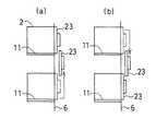
上記扉23は、扉開閉機構37によってローディングエリアS2側に移動して開き、更に上下方向に移動して退避するようになっている。二つのステージ11のうち、いずれか一方のステージ11のキャリア2のみ半導体ウエハWへのアクセスが可能とされ、他方のステージ11の扉23は閉鎖されている。具体的には図2に示すように、上部のステージ11の扉23が閉鎖されている時、下部のステージ11の扉23が開放されて上方に退避され、下部のステージ11の扉23が閉鎖されている時、上部のステージ11の扉23が開放されて下方に退避されるように構成されている。
【0023】
上記扉23は、図4に示すように、隔壁6の凹部35両外側部に対応するように延出された支持腕部42を有している。この扉23を上述のように開閉操作す扉開閉機構37は、隔壁6の凹部35両外側部に上下動ガイド43を介して上下移動可能に支持された上下可動枠44を有し、この上下可動枠44には前後動ガイド45を介して上記扉23の支持腕部42が前後移動可能に支持されている。上記上下可動枠44には、これを上下に駆動(昇降)するための扉昇降用エアシリンダ46が連結されている共に、支持腕部42を介して扉23を前後方向に開閉移動するための扉開閉用エアシリンダ47が取付けられている。図4の図示例では、一方(右側)の扉昇降用エアシリンダ47が上部の扉23を、他方(左側)の扉昇降用エアシリンダ47が下部の扉23をそれぞれ上下に駆動するようになっている。
【0024】
扉23が閉鎖した状態でキャリア2の蓋25の開閉を行うために、上記扉23には、扉23とは独立してキャリア2の蓋25の開閉を行うための蓋開閉機構48が設けられている。隔壁6は、蓋開閉機構48によりキャリア2の前面部から前方に移動されて開状態とされた蓋25を開口部22内に収容し得るスペースを確保する厚さに形成されている。上記蓋開閉機構48は、扉23のローディングエリア側の前面部に前後移動可能に配置された前後移動枠49を有し、この前後移動枠49に上記キー操作機構27が組込まれている。図示例の前後移動枠49は、扉23の両支持腕部42に対応するように延出された支持腕部50を有しており、この両支持腕部50が扉23の両支持腕部42に蓋開閉用のガイド付エアシリンダ51を介して前後移動可能に支持されている。
【0025】
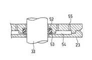
蓋開閉機構48の前後移動枠49に組込まれたキー操作機構27の回動軸33は、図7に示すように、扉23に対して前後方向に摺動可能および回動可能に貫通している。扉23には、上記回転軸33が貫通する貫通孔52が形成されており、この貫通孔52には、図9に示すように、回動軸貫通部の軸封手段として、Oリング等のシール部材53が設けられている。また、扉23には、上記回動軸貫通部から作業領域S1側の大気(空気)がローディングエリアS2側に漏れないようにすると共にキー28周縁部のパーティクル対策として、回動軸貫通部およびキー28周辺部を図示しない減圧ポンプにより減圧排気するための排気溝54および排気孔55が設けられている。
【0026】
上記扉23を閉鎖した状態で上記蓋開閉機構48により蓋25が開けられたキャリア2内を不活性ガスで置換するために、上記開口部22には不活性ガス置換手段56が設けられている。この不活性ガス置換手段56は、図8に示すように、開口部22の縁部に設けられた不活性ガス供給孔部57および排気孔部58からなっている。不活性ガスとしては、例えば窒素(N2)ガスが用いられる。キャリア2内および開口部22内を不活性ガスで円滑に置換するために、開口部22の左右対向縁部の一側に不活性ガス供給孔部57を、他側に排気孔部58をそれぞれ適宜間隔で設け、不活性ガスをキャリア2内の半導体ウエハWの面と平行に流すように構成することが好ましい。
【0027】
上記不活性ガス供給孔部57は不活性ガス供給管58を介して不活性ガス供給源に接続され、排気孔部58は排気管60を介して排気系に接続されている。上記排気管60には、図示しない酸素濃度センサが設けられており、酸素濃度が所定値まで下がった時に、不活性ガス置換作業を終了し、扉23を開放、退避するように構成されている。蓋25は、扉23と共に開放、退避される。蓋25の開閉、不活性ガスの置換、扉23の開閉等は、予め設定されたプログラムに基いて図示しない制御装置により制御されるように構成されている。なお、図7において、61はキャリア2と蓋25の間をシールするシール部材である。
【0028】
次に、作用ないし処理方法を述べる。先ず、キャリア搬送機構12によりキャリア2をステージ11上に搬送して載置する。キャリア2がステージ11上に載置されたことがキャリアセンサ39により検知されると、キャリア固定エアシリンダ40の駆動によりキャリア2が隔壁6の開口部22に押圧されて気密状態に当接固定される。この時、開口部22は扉23により予め閉鎖されており、キー28は隔壁6から突出しているとキャリア2と干渉するため予め開口部22内に引き込まれている。
【0029】
次に、図7(a)に示すように、扉23が閉鎖および蓋25が密閉されている状態で不活性ガス置換を行い、扉23と蓋25の間の大気を取り除いて不活性ガスを充満させる。その後で、上記扉23の閉鎖状態で上記キャリア2の蓋25を開け、キャリア2内を不活性ガス置換手段56により不活性ガスで置換する。この場合、蓋開閉機構48の作動により、図7(a)に示すように、前後移動枠19を介してキー28をキャリア2の蓋25側へ前進させ、キー28を蓋25の鍵穴29に挿入して回すことによりロックを解除する。この解除状態で、図7の(b)に示すように、キー28を後退させて蓋25を扉23に当接するまで開口部22内に引き込むことにより開ける。
【0030】
この状態で、不活性ガス置換手段56の不活性ガス供給孔部57から不活性ガス例えば窒素(N2)ガスを供給すると共に、排気孔部58から排気することにより、キャリア2内を不活性ガスで置換する。不活性ガスは、一側の不活性ガス供給孔部57からキャリア2と蓋25の隙間を通ってキャリア2内に入り、他側の排気孔部58より排気されることにより、キャリア2内および開口部22内に残存する空気を追い出してキャリア2内および開口部22内を不活性ガスで満たす。不活性ガスの供給を開始するタイミングは、キャリア2を開口部22に当接固定した時点からキャリア2の蓋25を開けた時点の間であれば何れでもよい。
【0031】
キャリア2内が不活性ガスで置換されたかどうかは、酸素濃度センサにより検知される。キャリア2内が不活性ガスで置換されると、不活性ガスの供給を停止し、図7の(c)に示すように、扉23と共に蓋25を開放して上下方向に退避させ、キャリア2内をローディングエリアS2側に開放する。次いで、キャリア2内の半導体ウエハWを移載機構19によりウエハボート4に移載し、キャリア2内の半導体ウエハWが空になったなら、扉23および蓋25を閉め、ステージ11上の空のキャリア2を保管部10のキャリア2と交換し、ウエハボート4に半導体ウエハWが所定枚数例えば100〜150枚程度移載されるまで上記作業を繰り返す。そして、上記ウエハボート4を熱処理炉5内に搬入して半導体ウエハWに所定の熱処理を施せばよい。熱処理が終了したなら、ウエハボート4を熱処理炉5から搬出し、上記とは逆の手順でウエハボート4から空のキャリア2内に処理済みの半導体ウエハWを移載すればよい。
【0032】
このように大気側と不活性ガス雰囲気のローディングエリアS2側を仕切る隔壁6の開口部22に蓋25で密閉されたキャリア2を大気側から当接させたなら、上記開口部22を閉鎖する扉23および上記キャリア2の蓋25を同時に開けるのではなく、先ず上記扉23を閉鎖したままの状態で上記蓋25のみを開けてキャリア2内を不活性ガスで置換してから、扉23および蓋25を開けてキャリア2内をローディングエリアS2側に開放するようにしたので、大気側の作業領域S1からローディングエリアS2への大気の侵入を防ぎ、またキャリア2内の空気がローディングエリアS2側に流出するのを未然に防止することができる。従って、ローディングエリアS2の不活性ガスの置換に時間がかからないばかりか、半導体ウエハWの自然酸化膜の発生等、プロセスへの影響もない。すなわち、キャリア2内の空気によってローディングエリアS2の酸素濃度を上げることなく半導体ウエハWの処理を行うことができ、スループットおよび歩留りの向上が図れる。
【0033】
以上、本発明の実施の形態を図面により詳述してきたが、本発明は上記実施の形態に限定されるものではなく、本発明の要旨を逸脱しない範囲での種々の設計変更等が可能である。例えば、キャリア固定手段としては、図10に示すようなキャリアロック機構64を採用してもよい。このキャリアロック機構64は、隔壁6の開口部22の近傍に支軸65を介して回動可能に軸支されたロックアーム66を有し、このロックアーム66を回動させてキャリア2のフランジ部26に当接させ、これを押圧固定するように構成されている。また、蓋開閉機構48としては、図11に示すように、支持腕部50を有しない前後移動枠49を用い、この前後移動枠49を扉23の前面部にエアシリンダ67を介して前後移動可能に設けた構成としてもよく、これにより構造の簡素化および省スペース化が図れる。
【0034】
【発明の効果】
以上要するに本発明によれば、次のような効果を奏することができる。
【0036】
(1)請求項1に係る発明によれば、大気側と不活性ガス雰囲気のローディングエリア側を仕切る隔壁の開口部に蓋で密閉されたキャリアを大気側から当接させたなら、上記開口部を閉鎖する扉および上記キャリアの蓋を同時に開けるのではなく、先ず上記扉と独立した蓋開閉機構により扉を閉鎖したままの状態で蓋のみを開け、キャリア内を不活性ガス置換手段により不活性ガスで置換してから、扉および蓋を開けてキャリア内をローディングエリア側に開放するようにしたので、簡単な構成で大気側の作業領域からローディングエリアへの大気の侵入を防ぎ、またキャリア内の空気がローディングエリア側に流出するのを確実に防止することができ、キャリア内の空気によってローディングエリアの酸素濃度を上げることなく被処理基板の処理を行うことが可能となる。
【図面の簡単な説明】
【図1】本発明を縦型熱処理装置に適用した実施の形態を示す概略的縦断面図である。
【図2】同縦型熱処理装置内の隔壁の開口部を閉鎖する扉の開放退避方法を説明する説明図である。
【図3】同縦型熱処理装置の概略的横断面図である。
【図4】扉および蓋の開閉機構を示す斜視図である。
【図5】キャリアおよびキー操作機構を示す斜視図である。
【図6】キャリアステージの近傍に配設された各種の機構を示す斜視図である。
【図7】蓋および扉の開閉方法を説明する説明図である。
【図8】不活性ガス置換手段の構成を示す概略的正面図である。
【図9】扉を貫通した回動軸の軸封手段の一例を示す部分的拡大断面図である。
【図10】キャリアを隔壁の開口部に固定する機構の他の例を示す図である。
【図11】蓋開閉機構の他の例を示す図である。
【符号の説明】
W 半導体ウエハ(被処理基板)
2 キャリア
6 隔壁
S2 ローディングエリア
22 開口部
23 扉
25 蓋
48 蓋開閉機構
56 不活性ガス置換手段
57 不活性ガス供給孔部
58 排気孔部[0001]
BACKGROUND OF THE INVENTION
The present invention relates to aprocessing device.
[0002]
[Prior art]
In the manufacture of a semiconductor device, there are processes for subjecting a semiconductor wafer as a substrate to be processed to various processes such as oxidation, diffusion, and CVD. For example, a heat treatment apparatus is used as an apparatus for performing such a process. In this heat treatment apparatus, an operator or an automatic transfer robot carries a work area for carrying a carrier containing a plurality of semiconductor wafers, and the semiconductor wafer in the carrier is transferred to a wafer boat as a substrate holder to carry it in and out of a heat treatment furnace. Loading area to perform.
[0003]
In such a heat treatment apparatus, in order to make the loading area a cleaner atmosphere than the work area and prevent the generation of a natural oxide film on the semiconductor wafer, the work area on the atmosphere side and the loading area are partitioned by a partition wall, and loading is performed. It is preferable to make the inside of the area an inert gas atmosphere filled with an inert gas such as nitrogen (N2 ) gas. Further, in order to suppress particle contamination of the semiconductor wafer, it is more preferable to apply a sealed carrier (also referred to as a closed carrier) in which the outlet of the semiconductor wafer is sealed with a lid.
[0004]
In this case, an opening for abutting the carrier from the work area side is formed in a partition partitioning the work area and the loading area, and a door for closing the opening is provided in the opening.When processing asemiconductor wafer, the carrier is set in the opening, the door of the opening and the lid of the carrier are opened, the inside of the carrier is opened to the loading area side, and the semiconductor wafer in the carrier is opened from the opening. May be transferred to the loading area side and transferred to a wafer boat, and the wafer boat may be carried into a heat treatment furnace to perform a predetermined heat treatment. JP-A-8-279546 discloses a technique for opening the door of the opening and the lid of the carrier together.
[0005]
[Problems to be solved by the invention]
By the way, the inside of the carrier is normally filled with the atmosphere, that is, air, unless the inside is specially replaced with an inert gas. Therefore, when the carrier is opened the cover of the carrier with the door is set tothe opening, the air in the carrier is considered to be flowing out in the loading area side. If the air in the carrier flows out to the loading area, the oxygen concentration in the loading area increases, so not only it takes time to replace the inert gas, but also the influence on the process, such as the generation of a natural oxide film on the semiconductor wafer. Is also a concern.
[0006]
Therefore, the present invention has been made to solve such problems. An object of the present invention, from the work area of the air side prevents air from entering the loading area, also provides aprocessing apparatusthat can be processed of the substrate to be processed without increasing the oxygen concentration in the loading area by the air in the carrier There is to do.
[0007]
[Means for Solving the Problems]
According to the first aspect of the present invention, a carrier in which a plurality of substrates to be processed are accommodated in an opening of a partition partitioning the atmosphere side and the loading area side of the inert gas atmosphere is sealed with a lid. From the opening, the door for closing the opening and the lid of the carrier are opened, the inside of the carrier is opened to the loading area side, and the substrate to be processed in the carrier is transferred from the opening to the loading area side for processing. In the processingapparatus ,a door opening / closing mechanism that opens the door to theloading area side and retracts in a vertical direction, a lid opening / closing mechanism that opens and closes the lid with the door closed, and a lid that is opened with the door closed. And an inert gas replacement means for replacing the inside of the carrier with an inert gas, and the lid opening / closing mechanism is arranged to move back and forth on the front surface portion on the loading area side of the door. And a key operation mechanism for locking or releasing the lid in the closed position by inserting and turning a key provided at the tip of the pivot shaft into the key hole of the lid. The rotating shaft penetrates the door so as to be slidable and rotatable in the front-rear direction .
[0008]
According to a second aspect of the present invention, inthe processing apparatus according to the first aspect, the door is provided with an exhaust groove and an exhaust hole for evacuating the rotary shaft penetrating portion and the key peripheral portion.
[0009]
In this case, itis preferable that the inert gas replacement means includes an inert gas supply hole and an exhaust hole provided at the edge of the opening.
The inert gas supply hole is provided on one side of the left and right edges of the opening, and the exhaust hole is provided on the other side at appropriate intervals, so that the inert gas is parallel to the surface of the substrate in the carrier. It is preferably configured to flow (claim 4).
It is preferable that an exhaust system is connected to the exhaust hole portion through an exhaust pipe, and an oxygen concentration sensor is provided in the exhaust pipe.
On the partition side, there are two stages for placing the carrier on the top and bottom, and thepartition has two openings on the top and bottom for contacting the carrier from the atmosphere side, and each opening is on the loading area side. When the upper stage door is closed, the lower stage door is opened and retracted upward, and the lower stage door is closed. It is preferable that the stage door is opened and retracted downward (Claim 6).
[0010]
Embodiment
Hereinafter, embodiments of the present invention will be described in detail with reference to the accompanying drawings. FIG. 1 is a schematic longitudinal sectional view showing an embodiment in which the present invention is applied to a vertical heat treatment apparatus, and FIG. 3 is a schematic cross sectional view of the vertical heat treatment apparatus.
[0011]
In these drawings,
[0012]
A loading /
[0013]
On the
[0014]
On the other hand, a vertical
[0015]
In the illustrated example, two
[0016]
The work area S <b> 1 is supplied with clean air through a filter (not shown) and has an atmospheric atmosphere. The loading area S2 is supplied with an inert gas such as nitrogen (N2 ) gas and has an inert gas atmosphere. In the
[0017]
The
[0018]
By inserting and rotating a key 28 of a key operation mechanism 27 (to be described later) into the
[0019]
The
[0020]
Specifically, a part of the
[0021]
On both sides of the
[0022]
The
[0023]
As shown in FIG. 4, the
[0024]
In order to open and close the
[0025]
As shown in FIG. 7, the
[0026]
In order to replace the inside of the
[0027]
The inert
[0028]
Next, the action or processing method will be described. First, the
[0029]
Next, as shown in FIG. 7A, the inert gas replacement is performed in a state where the
[0030]
In this state, an inert gas such as nitrogen (N2 ) gas is supplied from the inert
[0031]
Whether or not the inside of the
[0032]
Thus, if the
[0033]
Although the embodiments of the present invention have been described in detail with reference to the drawings, the present invention is not limited to the above-described embodiments, and various design changes and the like can be made without departing from the gist of the present invention. is there. For example, a
[0034]
【The invention's effect】
In short, according to the present invention, the following effects can be obtained.
[0036]
(1 ) According to theinvention of
[Brief description of the drawings]
FIG. 1 is a schematic longitudinal sectional view showing an embodiment in which the present invention is applied to a vertical heat treatment apparatus.
FIG. 2 is an explanatory view for explaining a door opening and closing method for closing an opening of a partition wall in the vertical heat treatment apparatus.
FIG. 3 is a schematic cross-sectional view of the vertical heat treatment apparatus.
FIG. 4 is a perspective view showing a door and lid opening / closing mechanism.
FIG. 5 is a perspective view showing a carrier and a key operation mechanism.
FIG. 6 is a perspective view showing various mechanisms arranged in the vicinity of the carrier stage.
FIG. 7 is an explanatory diagram for explaining a method of opening and closing a lid and a door.
FIG. 8 is a schematic front view showing a configuration of an inert gas replacement unit.
FIG. 9 is a partially enlarged cross-sectional view showing an example of a shaft sealing means for a rotating shaft penetrating a door.
FIG. 10 is a view showing another example of a mechanism for fixing the carrier to the opening of the partition wall.
FIG. 11 is a view showing another example of a lid opening / closing mechanism.
[Explanation of symbols]
W Semiconductor wafer (substrate to be processed)
2
Claims (6)
Translated fromJapanesePriority Applications (4)
| Application Number | Priority Date | Filing Date | Title |
|---|---|---|---|
| JP09400698AJP3656701B2 (en) | 1998-03-23 | 1998-03-23 | Processing equipment |
| US09/271,341US6231290B1 (en) | 1998-03-23 | 1999-03-18 | Processing method and processing unit for substrate |
| KR10-1999-0009815AKR100466920B1 (en) | 1998-03-23 | 1999-03-23 | Processing method and processing unit for substrate |
| US09/790,558US20010005476A1 (en) | 1998-03-23 | 2001-02-23 | Processing method and processing unit for substrate |
Applications Claiming Priority (1)
| Application Number | Priority Date | Filing Date | Title |
|---|---|---|---|
| JP09400698AJP3656701B2 (en) | 1998-03-23 | 1998-03-23 | Processing equipment |
Publications (2)
| Publication Number | Publication Date |
|---|---|
| JPH11274267A JPH11274267A (en) | 1999-10-08 |
| JP3656701B2true JP3656701B2 (en) | 2005-06-08 |
Family
ID=14098357
Family Applications (1)
| Application Number | Title | Priority Date | Filing Date |
|---|---|---|---|
| JP09400698AExpired - Fee RelatedJP3656701B2 (en) | 1998-03-23 | 1998-03-23 | Processing equipment |
Country Status (3)
| Country | Link |
|---|---|
| US (2) | US6231290B1 (en) |
| JP (1) | JP3656701B2 (en) |
| KR (1) | KR100466920B1 (en) |
Families Citing this family (345)
| Publication number | Priority date | Publication date | Assignee | Title |
|---|---|---|---|---|
| EP0735573B1 (en)* | 1995-03-28 | 2004-09-08 | BROOKS Automation GmbH | Loading and unloading station for semiconductor treatment installations |
| JP3664897B2 (en) | 1998-11-18 | 2005-06-29 | 東京エレクトロン株式会社 | Vertical heat treatment equipment |
| US6506009B1 (en)* | 2000-03-16 | 2003-01-14 | Applied Materials, Inc. | Apparatus for storing and moving a cassette |
| US6641350B2 (en)* | 2000-04-17 | 2003-11-04 | Hitachi Kokusai Electric Inc. | Dual loading port semiconductor processing equipment |
| KR100825134B1 (en)* | 2000-08-23 | 2008-04-24 | 도쿄엘렉트론가부시키가이샤 | Vertical Heat Treatment Equipment |
| TW522482B (en) | 2000-08-23 | 2003-03-01 | Tokyo Electron Ltd | Vertical heat treatment system, method for controlling vertical heat treatment system, and method for transferring object to be treated |
| JP2003183728A (en)* | 2001-12-14 | 2003-07-03 | Jh Corp | Vacuum heat-treatment apparatus |
| WO2003088351A1 (en)* | 2002-04-12 | 2003-10-23 | Tokyo Electron Limited | Port structure in semiconductor processing device |
| JP4218260B2 (en) | 2002-06-06 | 2009-02-04 | 東京エレクトロン株式会社 | Storage container body for processing object and processing system using the same |
| US7611319B2 (en)* | 2004-06-16 | 2009-11-03 | Applied Materials, Inc. | Methods and apparatus for identifying small lot size substrate carriers |
| WO2006029025A2 (en)* | 2004-09-04 | 2006-03-16 | Applied Materials, Inc. | Substrate carrier having reduced height |
| JP4534876B2 (en)* | 2005-06-13 | 2010-09-01 | シンフォニアテクノロジー株式会社 | SUBJECT SUPPLY APPARATUS AND SUBJECT SUPPLY METHOD |
| TW200725784A (en)* | 2005-11-21 | 2007-07-01 | Applied Materials Inc | Apparatus and methods for a substrate carrier having an inflatable seal |
| JP5259415B2 (en)* | 2005-11-23 | 2013-08-07 | サーフェス・コンバスチョン・インコーポレーテッド | Surface treatment of metal products in an atmospheric furnace |
| US20070141280A1 (en)* | 2005-12-16 | 2007-06-21 | Applied Materials, Inc. | Substrate carrier having an interior lining |
| JP5025231B2 (en)* | 2006-11-17 | 2012-09-12 | 東京エレクトロン株式会社 | Substrate transfer processing equipment |
| US9383036B2 (en)* | 2007-08-14 | 2016-07-05 | Parker-Hannifin Corporation | Bonded slit valve door seal with thin non-metallic film gap control bumper |
| JP2009049250A (en)* | 2007-08-22 | 2009-03-05 | Yaskawa Electric Corp | Cassette stage equipped with teaching mechanism, substrate transfer apparatus equipped with the same, semiconductor manufacturing apparatus |
| US8492283B2 (en)* | 2007-08-28 | 2013-07-23 | Taiwan Semiconductor Manufacturing Co., Ltd. | Method and structure for automated inert gas charging in a reticle stocker |
| JP5050761B2 (en) | 2007-10-03 | 2012-10-17 | 東京エレクトロン株式会社 | Processing system for object to be processed and heat treatment method for object to be processed |
| JP4821756B2 (en) | 2007-10-19 | 2011-11-24 | 東京エレクトロン株式会社 | To-be-processed object transfer mechanism, to-be-processed object transfer method, and to-be-processed object processing system |
| JP5134495B2 (en) | 2008-10-16 | 2013-01-30 | 東京エレクトロン株式会社 | Processing apparatus and processing method |
| US9394608B2 (en) | 2009-04-06 | 2016-07-19 | Asm America, Inc. | Semiconductor processing reactor and components thereof |
| US8802201B2 (en) | 2009-08-14 | 2014-08-12 | Asm America, Inc. | Systems and methods for thin-film deposition of metal oxides using excited nitrogen-oxygen species |
| JP5614352B2 (en)* | 2011-03-29 | 2014-10-29 | 東京エレクトロン株式会社 | Loading unit and processing system |
| US9312155B2 (en) | 2011-06-06 | 2016-04-12 | Asm Japan K.K. | High-throughput semiconductor-processing apparatus equipped with multiple dual-chamber modules |
| US10854498B2 (en) | 2011-07-15 | 2020-12-01 | Asm Ip Holding B.V. | Wafer-supporting device and method for producing same |
| US20130023129A1 (en) | 2011-07-20 | 2013-01-24 | Asm America, Inc. | Pressure transmitter for a semiconductor processing environment |
| US9017481B1 (en) | 2011-10-28 | 2015-04-28 | Asm America, Inc. | Process feed management for semiconductor substrate processing |
| TW201320230A (en)* | 2011-11-09 | 2013-05-16 | Sinfonia Technology Co Ltd | Load port and efem |
| JP6045946B2 (en)* | 2012-07-13 | 2016-12-14 | 株式会社Screenホールディングス | Substrate processing apparatus, program and recording medium |
| US10714315B2 (en) | 2012-10-12 | 2020-07-14 | Asm Ip Holdings B.V. | Semiconductor reaction chamber showerhead |
| US20160376700A1 (en) | 2013-02-01 | 2016-12-29 | Asm Ip Holding B.V. | System for treatment of deposition reactor |
| US10683571B2 (en) | 2014-02-25 | 2020-06-16 | Asm Ip Holding B.V. | Gas supply manifold and method of supplying gases to chamber using same |
| US10167557B2 (en) | 2014-03-18 | 2019-01-01 | Asm Ip Holding B.V. | Gas distribution system, reactor including the system, and methods of using the same |
| US11015245B2 (en) | 2014-03-19 | 2021-05-25 | Asm Ip Holding B.V. | Gas-phase reactor and system having exhaust plenum and components thereof |
| US10858737B2 (en) | 2014-07-28 | 2020-12-08 | Asm Ip Holding B.V. | Showerhead assembly and components thereof |
| US9890456B2 (en) | 2014-08-21 | 2018-02-13 | Asm Ip Holding B.V. | Method and system for in situ formation of gas-phase compounds |
| US10941490B2 (en) | 2014-10-07 | 2021-03-09 | Asm Ip Holding B.V. | Multiple temperature range susceptor, assembly, reactor and system including the susceptor, and methods of using the same |
| US9657845B2 (en) | 2014-10-07 | 2017-05-23 | Asm Ip Holding B.V. | Variable conductance gas distribution apparatus and method |
| US10276355B2 (en) | 2015-03-12 | 2019-04-30 | Asm Ip Holding B.V. | Multi-zone reactor, system including the reactor, and method of using the same |
| US10458018B2 (en) | 2015-06-26 | 2019-10-29 | Asm Ip Holding B.V. | Structures including metal carbide material, devices including the structures, and methods of forming same |
| US10600673B2 (en) | 2015-07-07 | 2020-03-24 | Asm Ip Holding B.V. | Magnetic susceptor to baseplate seal |
| US10211308B2 (en) | 2015-10-21 | 2019-02-19 | Asm Ip Holding B.V. | NbMC layers |
| US11139308B2 (en) | 2015-12-29 | 2021-10-05 | Asm Ip Holding B.V. | Atomic layer deposition of III-V compounds to form V-NAND devices |
| US10529554B2 (en) | 2016-02-19 | 2020-01-07 | Asm Ip Holding B.V. | Method for forming silicon nitride film selectively on sidewalls or flat surfaces of trenches |
| US10343920B2 (en) | 2016-03-18 | 2019-07-09 | Asm Ip Holding B.V. | Aligned carbon nanotubes |
| US10190213B2 (en) | 2016-04-21 | 2019-01-29 | Asm Ip Holding B.V. | Deposition of metal borides |
| US10865475B2 (en) | 2016-04-21 | 2020-12-15 | Asm Ip Holding B.V. | Deposition of metal borides and silicides |
| US10367080B2 (en) | 2016-05-02 | 2019-07-30 | Asm Ip Holding B.V. | Method of forming a germanium oxynitride film |
| US10032628B2 (en) | 2016-05-02 | 2018-07-24 | Asm Ip Holding B.V. | Source/drain performance through conformal solid state doping |
| US11453943B2 (en) | 2016-05-25 | 2022-09-27 | Asm Ip Holding B.V. | Method for forming carbon-containing silicon/metal oxide or nitride film by ALD using silicon precursor and hydrocarbon precursor |
| US9859151B1 (en) | 2016-07-08 | 2018-01-02 | Asm Ip Holding B.V. | Selective film deposition method to form air gaps |
| US10612137B2 (en) | 2016-07-08 | 2020-04-07 | Asm Ip Holdings B.V. | Organic reactants for atomic layer deposition |
| US10714385B2 (en) | 2016-07-19 | 2020-07-14 | Asm Ip Holding B.V. | Selective deposition of tungsten |
| KR102532607B1 (en) | 2016-07-28 | 2023-05-15 | 에이에스엠 아이피 홀딩 비.브이. | Substrate processing apparatus and method of operating the same |
| US9887082B1 (en) | 2016-07-28 | 2018-02-06 | Asm Ip Holding B.V. | Method and apparatus for filling a gap |
| US9812320B1 (en) | 2016-07-28 | 2017-11-07 | Asm Ip Holding B.V. | Method and apparatus for filling a gap |
| US10643826B2 (en) | 2016-10-26 | 2020-05-05 | Asm Ip Holdings B.V. | Methods for thermally calibrating reaction chambers |
| US11532757B2 (en) | 2016-10-27 | 2022-12-20 | Asm Ip Holding B.V. | Deposition of charge trapping layers |
| US10229833B2 (en) | 2016-11-01 | 2019-03-12 | Asm Ip Holding B.V. | Methods for forming a transition metal nitride film on a substrate by atomic layer deposition and related semiconductor device structures |
| US10643904B2 (en) | 2016-11-01 | 2020-05-05 | Asm Ip Holdings B.V. | Methods for forming a semiconductor device and related semiconductor device structures |
| US10714350B2 (en) | 2016-11-01 | 2020-07-14 | ASM IP Holdings, B.V. | Methods for forming a transition metal niobium nitride film on a substrate by atomic layer deposition and related semiconductor device structures |
| US10134757B2 (en) | 2016-11-07 | 2018-11-20 | Asm Ip Holding B.V. | Method of processing a substrate and a device manufactured by using the method |
| KR102546317B1 (en) | 2016-11-15 | 2023-06-21 | 에이에스엠 아이피 홀딩 비.브이. | Gas supply unit and substrate processing apparatus including the same |
| KR102762543B1 (en) | 2016-12-14 | 2025-02-05 | 에이에스엠 아이피 홀딩 비.브이. | Substrate processing apparatus |
| US11581186B2 (en) | 2016-12-15 | 2023-02-14 | Asm Ip Holding B.V. | Sequential infiltration synthesis apparatus |
| US11447861B2 (en) | 2016-12-15 | 2022-09-20 | Asm Ip Holding B.V. | Sequential infiltration synthesis apparatus and a method of forming a patterned structure |
| KR102700194B1 (en) | 2016-12-19 | 2024-08-28 | 에이에스엠 아이피 홀딩 비.브이. | Substrate processing apparatus |
| US10269558B2 (en) | 2016-12-22 | 2019-04-23 | Asm Ip Holding B.V. | Method of forming a structure on a substrate |
| US10867788B2 (en) | 2016-12-28 | 2020-12-15 | Asm Ip Holding B.V. | Method of forming a structure on a substrate |
| US11390950B2 (en) | 2017-01-10 | 2022-07-19 | Asm Ip Holding B.V. | Reactor system and method to reduce residue buildup during a film deposition process |
| US10655221B2 (en) | 2017-02-09 | 2020-05-19 | Asm Ip Holding B.V. | Method for depositing oxide film by thermal ALD and PEALD |
| US10468261B2 (en) | 2017-02-15 | 2019-11-05 | Asm Ip Holding B.V. | Methods for forming a metallic film on a substrate by cyclical deposition and related semiconductor device structures |
| US10529563B2 (en) | 2017-03-29 | 2020-01-07 | Asm Ip Holdings B.V. | Method for forming doped metal oxide films on a substrate by cyclical deposition and related semiconductor device structures |
| USD876504S1 (en) | 2017-04-03 | 2020-02-25 | Asm Ip Holding B.V. | Exhaust flow control ring for semiconductor deposition apparatus |
| KR102457289B1 (en) | 2017-04-25 | 2022-10-21 | 에이에스엠 아이피 홀딩 비.브이. | Method for depositing a thin film and manufacturing a semiconductor device |
| US10892156B2 (en) | 2017-05-08 | 2021-01-12 | Asm Ip Holding B.V. | Methods for forming a silicon nitride film on a substrate and related semiconductor device structures |
| US10770286B2 (en) | 2017-05-08 | 2020-09-08 | Asm Ip Holdings B.V. | Methods for selectively forming a silicon nitride film on a substrate and related semiconductor device structures |
| US12040200B2 (en) | 2017-06-20 | 2024-07-16 | Asm Ip Holding B.V. | Semiconductor processing apparatus and methods for calibrating a semiconductor processing apparatus |
| US11306395B2 (en) | 2017-06-28 | 2022-04-19 | Asm Ip Holding B.V. | Methods for depositing a transition metal nitride film on a substrate by atomic layer deposition and related deposition apparatus |
| US10685834B2 (en) | 2017-07-05 | 2020-06-16 | Asm Ip Holdings B.V. | Methods for forming a silicon germanium tin layer and related semiconductor device structures |
| KR20190009245A (en) | 2017-07-18 | 2019-01-28 | 에이에스엠 아이피 홀딩 비.브이. | Methods for forming a semiconductor device structure and related semiconductor device structures |
| US11374112B2 (en) | 2017-07-19 | 2022-06-28 | Asm Ip Holding B.V. | Method for depositing a group IV semiconductor and related semiconductor device structures |
| US11018002B2 (en) | 2017-07-19 | 2021-05-25 | Asm Ip Holding B.V. | Method for selectively depositing a Group IV semiconductor and related semiconductor device structures |
| US10541333B2 (en) | 2017-07-19 | 2020-01-21 | Asm Ip Holding B.V. | Method for depositing a group IV semiconductor and related semiconductor device structures |
| US10590535B2 (en) | 2017-07-26 | 2020-03-17 | Asm Ip Holdings B.V. | Chemical treatment, deposition and/or infiltration apparatus and method for using the same |
| TWI815813B (en) | 2017-08-04 | 2023-09-21 | 荷蘭商Asm智慧財產控股公司 | Showerhead assembly for distributing a gas within a reaction chamber |
| US10692741B2 (en) | 2017-08-08 | 2020-06-23 | Asm Ip Holdings B.V. | Radiation shield |
| US10770336B2 (en) | 2017-08-08 | 2020-09-08 | Asm Ip Holding B.V. | Substrate lift mechanism and reactor including same |
| US10249524B2 (en) | 2017-08-09 | 2019-04-02 | Asm Ip Holding B.V. | Cassette holder assembly for a substrate cassette and holding member for use in such assembly |
| US11139191B2 (en) | 2017-08-09 | 2021-10-05 | Asm Ip Holding B.V. | Storage apparatus for storing cassettes for substrates and processing apparatus equipped therewith |
| US11769682B2 (en) | 2017-08-09 | 2023-09-26 | Asm Ip Holding B.V. | Storage apparatus for storing cassettes for substrates and processing apparatus equipped therewith |
| USD900036S1 (en) | 2017-08-24 | 2020-10-27 | Asm Ip Holding B.V. | Heater electrical connector and adapter |
| US11830730B2 (en) | 2017-08-29 | 2023-11-28 | Asm Ip Holding B.V. | Layer forming method and apparatus |
| US11056344B2 (en) | 2017-08-30 | 2021-07-06 | Asm Ip Holding B.V. | Layer forming method |
| US11295980B2 (en) | 2017-08-30 | 2022-04-05 | Asm Ip Holding B.V. | Methods for depositing a molybdenum metal film over a dielectric surface of a substrate by a cyclical deposition process and related semiconductor device structures |
| KR102491945B1 (en) | 2017-08-30 | 2023-01-26 | 에이에스엠 아이피 홀딩 비.브이. | Substrate processing apparatus |
| KR102401446B1 (en) | 2017-08-31 | 2022-05-24 | 에이에스엠 아이피 홀딩 비.브이. | Substrate processing apparatus |
| KR102630301B1 (en) | 2017-09-21 | 2024-01-29 | 에이에스엠 아이피 홀딩 비.브이. | Method of sequential infiltration synthesis treatment of infiltrateable material and structures and devices formed using same |
| US10844484B2 (en) | 2017-09-22 | 2020-11-24 | Asm Ip Holding B.V. | Apparatus for dispensing a vapor phase reactant to a reaction chamber and related methods |
| JP6939335B2 (en)* | 2017-09-27 | 2021-09-22 | Tdk株式会社 | Load port device, how to drive the load port device |
| US10658205B2 (en) | 2017-09-28 | 2020-05-19 | Asm Ip Holdings B.V. | Chemical dispensing apparatus and methods for dispensing a chemical to a reaction chamber |
| US10403504B2 (en) | 2017-10-05 | 2019-09-03 | Asm Ip Holding B.V. | Method for selectively depositing a metallic film on a substrate |
| US10319588B2 (en) | 2017-10-10 | 2019-06-11 | Asm Ip Holding B.V. | Method for depositing a metal chalcogenide on a substrate by cyclical deposition |
| US10923344B2 (en) | 2017-10-30 | 2021-02-16 | Asm Ip Holding B.V. | Methods for forming a semiconductor structure and related semiconductor structures |
| US10910262B2 (en) | 2017-11-16 | 2021-02-02 | Asm Ip Holding B.V. | Method of selectively depositing a capping layer structure on a semiconductor device structure |
| KR102443047B1 (en) | 2017-11-16 | 2022-09-14 | 에이에스엠 아이피 홀딩 비.브이. | Method of processing a substrate and a device manufactured by the same |
| US11022879B2 (en) | 2017-11-24 | 2021-06-01 | Asm Ip Holding B.V. | Method of forming an enhanced unexposed photoresist layer |
| CN111344522B (en) | 2017-11-27 | 2022-04-12 | 阿斯莫Ip控股公司 | Including clean mini-environment device |
| WO2019103613A1 (en) | 2017-11-27 | 2019-05-31 | Asm Ip Holding B.V. | A storage device for storing wafer cassettes for use with a batch furnace |
| US10872771B2 (en) | 2018-01-16 | 2020-12-22 | Asm Ip Holding B. V. | Method for depositing a material film on a substrate within a reaction chamber by a cyclical deposition process and related device structures |
| KR102695659B1 (en) | 2018-01-19 | 2024-08-14 | 에이에스엠 아이피 홀딩 비.브이. | Method for depositing a gap filling layer by plasma assisted deposition |
| TWI799494B (en) | 2018-01-19 | 2023-04-21 | 荷蘭商Asm 智慧財產控股公司 | Deposition method |
| USD903477S1 (en) | 2018-01-24 | 2020-12-01 | Asm Ip Holdings B.V. | Metal clamp |
| US11018047B2 (en) | 2018-01-25 | 2021-05-25 | Asm Ip Holding B.V. | Hybrid lift pin |
| USD880437S1 (en) | 2018-02-01 | 2020-04-07 | Asm Ip Holding B.V. | Gas supply plate for semiconductor manufacturing apparatus |
| US11081345B2 (en) | 2018-02-06 | 2021-08-03 | Asm Ip Holding B.V. | Method of post-deposition treatment for silicon oxide film |
| US10896820B2 (en) | 2018-02-14 | 2021-01-19 | Asm Ip Holding B.V. | Method for depositing a ruthenium-containing film on a substrate by a cyclical deposition process |
| WO2019158960A1 (en) | 2018-02-14 | 2019-08-22 | Asm Ip Holding B.V. | A method for depositing a ruthenium-containing film on a substrate by a cyclical deposition process |
| US10731249B2 (en) | 2018-02-15 | 2020-08-04 | Asm Ip Holding B.V. | Method of forming a transition metal containing film on a substrate by a cyclical deposition process, a method for supplying a transition metal halide compound to a reaction chamber, and related vapor deposition apparatus |
| KR102636427B1 (en) | 2018-02-20 | 2024-02-13 | 에이에스엠 아이피 홀딩 비.브이. | Substrate processing method and apparatus |
| US10658181B2 (en) | 2018-02-20 | 2020-05-19 | Asm Ip Holding B.V. | Method of spacer-defined direct patterning in semiconductor fabrication |
| US10975470B2 (en) | 2018-02-23 | 2021-04-13 | Asm Ip Holding B.V. | Apparatus for detecting or monitoring for a chemical precursor in a high temperature environment |
| US11473195B2 (en) | 2018-03-01 | 2022-10-18 | Asm Ip Holding B.V. | Semiconductor processing apparatus and a method for processing a substrate |
| US11629406B2 (en) | 2018-03-09 | 2023-04-18 | Asm Ip Holding B.V. | Semiconductor processing apparatus comprising one or more pyrometers for measuring a temperature of a substrate during transfer of the substrate |
| US11114283B2 (en) | 2018-03-16 | 2021-09-07 | Asm Ip Holding B.V. | Reactor, system including the reactor, and methods of manufacturing and using same |
| KR102646467B1 (en) | 2018-03-27 | 2024-03-11 | 에이에스엠 아이피 홀딩 비.브이. | Method of forming an electrode on a substrate and a semiconductor device structure including an electrode |
| US11088002B2 (en) | 2018-03-29 | 2021-08-10 | Asm Ip Holding B.V. | Substrate rack and a substrate processing system and method |
| US11230766B2 (en) | 2018-03-29 | 2022-01-25 | Asm Ip Holding B.V. | Substrate processing apparatus and method |
| KR102501472B1 (en) | 2018-03-30 | 2023-02-20 | 에이에스엠 아이피 홀딩 비.브이. | Substrate processing method |
| KR102600229B1 (en) | 2018-04-09 | 2023-11-10 | 에이에스엠 아이피 홀딩 비.브이. | Substrate supporting device, substrate processing apparatus including the same and substrate processing method |
| TWI811348B (en) | 2018-05-08 | 2023-08-11 | 荷蘭商Asm 智慧財產控股公司 | Methods for depositing an oxide film on a substrate by a cyclical deposition process and related device structures |
| US12025484B2 (en) | 2018-05-08 | 2024-07-02 | Asm Ip Holding B.V. | Thin film forming method |
| US12272527B2 (en) | 2018-05-09 | 2025-04-08 | Asm Ip Holding B.V. | Apparatus for use with hydrogen radicals and method of using same |
| KR20190129718A (en) | 2018-05-11 | 2019-11-20 | 에이에스엠 아이피 홀딩 비.브이. | Methods for forming a doped metal carbide film on a substrate and related semiconductor device structures |
| KR102596988B1 (en) | 2018-05-28 | 2023-10-31 | 에이에스엠 아이피 홀딩 비.브이. | Method of processing a substrate and a device manufactured by the same |
| US11718913B2 (en) | 2018-06-04 | 2023-08-08 | Asm Ip Holding B.V. | Gas distribution system and reactor system including same |
| TWI840362B (en) | 2018-06-04 | 2024-05-01 | 荷蘭商Asm Ip私人控股有限公司 | Wafer handling chamber with moisture reduction |
| US11286562B2 (en) | 2018-06-08 | 2022-03-29 | Asm Ip Holding B.V. | Gas-phase chemical reactor and method of using same |
| KR102568797B1 (en) | 2018-06-21 | 2023-08-21 | 에이에스엠 아이피 홀딩 비.브이. | Substrate processing system |
| US10797133B2 (en) | 2018-06-21 | 2020-10-06 | Asm Ip Holding B.V. | Method for depositing a phosphorus doped silicon arsenide film and related semiconductor device structures |
| TWI873894B (en) | 2018-06-27 | 2025-02-21 | 荷蘭商Asm Ip私人控股有限公司 | Cyclic deposition methods for forming metal-containing material and films and structures including the metal-containing material |
| KR102854019B1 (en) | 2018-06-27 | 2025-09-02 | 에이에스엠 아이피 홀딩 비.브이. | Periodic deposition method for forming a metal-containing material and films and structures comprising the metal-containing material |
| KR102686758B1 (en) | 2018-06-29 | 2024-07-18 | 에이에스엠 아이피 홀딩 비.브이. | Method for depositing a thin film and manufacturing a semiconductor device |
| US10612136B2 (en) | 2018-06-29 | 2020-04-07 | ASM IP Holding, B.V. | Temperature-controlled flange and reactor system including same |
| US10755922B2 (en) | 2018-07-03 | 2020-08-25 | Asm Ip Holding B.V. | Method for depositing silicon-free carbon-containing film as gap-fill layer by pulse plasma-assisted deposition |
| US10388513B1 (en) | 2018-07-03 | 2019-08-20 | Asm Ip Holding B.V. | Method for depositing silicon-free carbon-containing film as gap-fill layer by pulse plasma-assisted deposition |
| US10767789B2 (en) | 2018-07-16 | 2020-09-08 | Asm Ip Holding B.V. | Diaphragm valves, valve components, and methods for forming valve components |
| US11053591B2 (en) | 2018-08-06 | 2021-07-06 | Asm Ip Holding B.V. | Multi-port gas injection system and reactor system including same |
| US10883175B2 (en) | 2018-08-09 | 2021-01-05 | Asm Ip Holding B.V. | Vertical furnace for processing substrates and a liner for use therein |
| US10829852B2 (en) | 2018-08-16 | 2020-11-10 | Asm Ip Holding B.V. | Gas distribution device for a wafer processing apparatus |
| US11430674B2 (en) | 2018-08-22 | 2022-08-30 | Asm Ip Holding B.V. | Sensor array, apparatus for dispensing a vapor phase reactant to a reaction chamber and related methods |
| US11024523B2 (en) | 2018-09-11 | 2021-06-01 | Asm Ip Holding B.V. | Substrate processing apparatus and method |
| KR102707956B1 (en) | 2018-09-11 | 2024-09-19 | 에이에스엠 아이피 홀딩 비.브이. | Method for deposition of a thin film |
| US11049751B2 (en) | 2018-09-14 | 2021-06-29 | Asm Ip Holding B.V. | Cassette supply system to store and handle cassettes and processing apparatus equipped therewith |
| CN110970344B (en) | 2018-10-01 | 2024-10-25 | Asmip控股有限公司 | Substrate holding apparatus, system comprising the same and method of using the same |
| US11232963B2 (en) | 2018-10-03 | 2022-01-25 | Asm Ip Holding B.V. | Substrate processing apparatus and method |
| KR102592699B1 (en) | 2018-10-08 | 2023-10-23 | 에이에스엠 아이피 홀딩 비.브이. | Substrate support unit and apparatuses for depositing thin film and processing the substrate including the same |
| US10847365B2 (en) | 2018-10-11 | 2020-11-24 | Asm Ip Holding B.V. | Method of forming conformal silicon carbide film by cyclic CVD |
| US10811256B2 (en) | 2018-10-16 | 2020-10-20 | Asm Ip Holding B.V. | Method for etching a carbon-containing feature |
| KR102546322B1 (en) | 2018-10-19 | 2023-06-21 | 에이에스엠 아이피 홀딩 비.브이. | Substrate processing apparatus and substrate processing method |
| KR102605121B1 (en) | 2018-10-19 | 2023-11-23 | 에이에스엠 아이피 홀딩 비.브이. | Substrate processing apparatus and substrate processing method |
| USD948463S1 (en) | 2018-10-24 | 2022-04-12 | Asm Ip Holding B.V. | Susceptor for semiconductor substrate supporting apparatus |
| US12378665B2 (en) | 2018-10-26 | 2025-08-05 | Asm Ip Holding B.V. | High temperature coatings for a preclean and etch apparatus and related methods |
| US11087997B2 (en) | 2018-10-31 | 2021-08-10 | Asm Ip Holding B.V. | Substrate processing apparatus for processing substrates |
| KR102748291B1 (en) | 2018-11-02 | 2024-12-31 | 에이에스엠 아이피 홀딩 비.브이. | Substrate support unit and substrate processing apparatus including the same |
| US11572620B2 (en) | 2018-11-06 | 2023-02-07 | Asm Ip Holding B.V. | Methods for selectively depositing an amorphous silicon film on a substrate |
| US11031242B2 (en) | 2018-11-07 | 2021-06-08 | Asm Ip Holding B.V. | Methods for depositing a boron doped silicon germanium film |
| US10818758B2 (en) | 2018-11-16 | 2020-10-27 | Asm Ip Holding B.V. | Methods for forming a metal silicate film on a substrate in a reaction chamber and related semiconductor device structures |
| US10847366B2 (en) | 2018-11-16 | 2020-11-24 | Asm Ip Holding B.V. | Methods for depositing a transition metal chalcogenide film on a substrate by a cyclical deposition process |
| US10559458B1 (en) | 2018-11-26 | 2020-02-11 | Asm Ip Holding B.V. | Method of forming oxynitride film |
| US12040199B2 (en) | 2018-11-28 | 2024-07-16 | Asm Ip Holding B.V. | Substrate processing apparatus for processing substrates |
| US11217444B2 (en) | 2018-11-30 | 2022-01-04 | Asm Ip Holding B.V. | Method for forming an ultraviolet radiation responsive metal oxide-containing film |
| KR102636428B1 (en) | 2018-12-04 | 2024-02-13 | 에이에스엠 아이피 홀딩 비.브이. | A method for cleaning a substrate processing apparatus |
| US11158513B2 (en) | 2018-12-13 | 2021-10-26 | Asm Ip Holding B.V. | Methods for forming a rhenium-containing film on a substrate by a cyclical deposition process and related semiconductor device structures |
| TWI874340B (en) | 2018-12-14 | 2025-03-01 | 荷蘭商Asm Ip私人控股有限公司 | Method of forming device structure, structure formed by the method and system for performing the method |
| TWI866480B (en) | 2019-01-17 | 2024-12-11 | 荷蘭商Asm Ip 私人控股有限公司 | Methods of forming a transition metal containing film on a substrate by a cyclical deposition process |
| KR102727227B1 (en) | 2019-01-22 | 2024-11-07 | 에이에스엠 아이피 홀딩 비.브이. | Semiconductor processing device |
| CN111524788B (en) | 2019-02-01 | 2023-11-24 | Asm Ip私人控股有限公司 | Method for forming topologically selective films of silicon oxide |
| TWI845607B (en) | 2019-02-20 | 2024-06-21 | 荷蘭商Asm Ip私人控股有限公司 | Cyclical deposition method and apparatus for filling a recess formed within a substrate surface |
| TWI838458B (en) | 2019-02-20 | 2024-04-11 | 荷蘭商Asm Ip私人控股有限公司 | Apparatus and methods for plug fill deposition in 3-d nand applications |
| KR102626263B1 (en) | 2019-02-20 | 2024-01-16 | 에이에스엠 아이피 홀딩 비.브이. | Cyclical deposition method including treatment step and apparatus for same |
| TWI873122B (en) | 2019-02-20 | 2025-02-21 | 荷蘭商Asm Ip私人控股有限公司 | Method of filling a recess formed within a surface of a substrate, semiconductor structure formed according to the method, and semiconductor processing apparatus |
| TWI842826B (en) | 2019-02-22 | 2024-05-21 | 荷蘭商Asm Ip私人控股有限公司 | Substrate processing apparatus and method for processing substrate |
| KR102782593B1 (en) | 2019-03-08 | 2025-03-14 | 에이에스엠 아이피 홀딩 비.브이. | Structure Including SiOC Layer and Method of Forming Same |
| KR102858005B1 (en) | 2019-03-08 | 2025-09-09 | 에이에스엠 아이피 홀딩 비.브이. | Method for Selective Deposition of Silicon Nitride Layer and Structure Including Selectively-Deposited Silicon Nitride Layer |
| US11742198B2 (en) | 2019-03-08 | 2023-08-29 | Asm Ip Holding B.V. | Structure including SiOCN layer and method of forming same |
| JP2020167398A (en) | 2019-03-28 | 2020-10-08 | エーエスエム・アイピー・ホールディング・ベー・フェー | Door openers and substrate processing equipment provided with door openers |
| KR102809999B1 (en) | 2019-04-01 | 2025-05-19 | 에이에스엠 아이피 홀딩 비.브이. | Method of manufacturing semiconductor device |
| KR20200123380A (en) | 2019-04-19 | 2020-10-29 | 에이에스엠 아이피 홀딩 비.브이. | Layer forming method and apparatus |
| KR20200125453A (en) | 2019-04-24 | 2020-11-04 | 에이에스엠 아이피 홀딩 비.브이. | Gas-phase reactor system and method of using same |
| US11289326B2 (en) | 2019-05-07 | 2022-03-29 | Asm Ip Holding B.V. | Method for reforming amorphous carbon polymer film |
| KR20200130121A (en) | 2019-05-07 | 2020-11-18 | 에이에스엠 아이피 홀딩 비.브이. | Chemical source vessel with dip tube |
| KR20200130652A (en) | 2019-05-10 | 2020-11-19 | 에이에스엠 아이피 홀딩 비.브이. | Method of depositing material onto a surface and structure formed according to the method |
| JP7612342B2 (en) | 2019-05-16 | 2025-01-14 | エーエスエム・アイピー・ホールディング・ベー・フェー | Wafer boat handling apparatus, vertical batch furnace and method |
| JP7598201B2 (en) | 2019-05-16 | 2024-12-11 | エーエスエム・アイピー・ホールディング・ベー・フェー | Wafer boat handling apparatus, vertical batch furnace and method |
| USD975665S1 (en) | 2019-05-17 | 2023-01-17 | Asm Ip Holding B.V. | Susceptor shaft |
| USD947913S1 (en) | 2019-05-17 | 2022-04-05 | Asm Ip Holding B.V. | Susceptor shaft |
| USD935572S1 (en) | 2019-05-24 | 2021-11-09 | Asm Ip Holding B.V. | Gas channel plate |
| USD922229S1 (en) | 2019-06-05 | 2021-06-15 | Asm Ip Holding B.V. | Device for controlling a temperature of a gas supply unit |
| KR20200141002A (en) | 2019-06-06 | 2020-12-17 | 에이에스엠 아이피 홀딩 비.브이. | Method of using a gas-phase reactor system including analyzing exhausted gas |
| KR20200141931A (en) | 2019-06-10 | 2020-12-21 | 에이에스엠 아이피 홀딩 비.브이. | Method for cleaning quartz epitaxial chambers |
| KR20200143254A (en) | 2019-06-11 | 2020-12-23 | 에이에스엠 아이피 홀딩 비.브이. | Method of forming an electronic structure using an reforming gas, system for performing the method, and structure formed using the method |
| USD944946S1 (en) | 2019-06-14 | 2022-03-01 | Asm Ip Holding B.V. | Shower plate |
| USD931978S1 (en) | 2019-06-27 | 2021-09-28 | Asm Ip Holding B.V. | Showerhead vacuum transport |
| KR20210005515A (en) | 2019-07-03 | 2021-01-14 | 에이에스엠 아이피 홀딩 비.브이. | Temperature control assembly for substrate processing apparatus and method of using same |
| JP7499079B2 (en) | 2019-07-09 | 2024-06-13 | エーエスエム・アイピー・ホールディング・ベー・フェー | Plasma device using coaxial waveguide and substrate processing method |
| CN112216646A (en) | 2019-07-10 | 2021-01-12 | Asm Ip私人控股有限公司 | Substrate supporting assembly and substrate processing device comprising same |
| KR20210010307A (en) | 2019-07-16 | 2021-01-27 | 에이에스엠 아이피 홀딩 비.브이. | Substrate processing apparatus |
| KR20210010816A (en) | 2019-07-17 | 2021-01-28 | 에이에스엠 아이피 홀딩 비.브이. | Radical assist ignition plasma system and method |
| KR102860110B1 (en) | 2019-07-17 | 2025-09-16 | 에이에스엠 아이피 홀딩 비.브이. | Methods of forming silicon germanium structures |
| US11643724B2 (en) | 2019-07-18 | 2023-05-09 | Asm Ip Holding B.V. | Method of forming structures using a neutral beam |
| TWI839544B (en) | 2019-07-19 | 2024-04-21 | 荷蘭商Asm Ip私人控股有限公司 | Method of forming topology-controlled amorphous carbon polymer film |
| KR20210010817A (en) | 2019-07-19 | 2021-01-28 | 에이에스엠 아이피 홀딩 비.브이. | Method of Forming Topology-Controlled Amorphous Carbon Polymer Film |
| TWI851767B (en) | 2019-07-29 | 2024-08-11 | 荷蘭商Asm Ip私人控股有限公司 | Methods for selective deposition utilizing n-type dopants and/or alternative dopants to achieve high dopant incorporation |
| CN112309899A (en) | 2019-07-30 | 2021-02-02 | Asm Ip私人控股有限公司 | Substrate processing apparatus |
| CN112309900A (en) | 2019-07-30 | 2021-02-02 | Asm Ip私人控股有限公司 | Substrate processing apparatus |
| US12169361B2 (en) | 2019-07-30 | 2024-12-17 | Asm Ip Holding B.V. | Substrate processing apparatus and method |
| US11227782B2 (en) | 2019-07-31 | 2022-01-18 | Asm Ip Holding B.V. | Vertical batch furnace assembly |
| US11587814B2 (en) | 2019-07-31 | 2023-02-21 | Asm Ip Holding B.V. | Vertical batch furnace assembly |
| US11587815B2 (en) | 2019-07-31 | 2023-02-21 | Asm Ip Holding B.V. | Vertical batch furnace assembly |
| CN112323048B (en) | 2019-08-05 | 2024-02-09 | Asm Ip私人控股有限公司 | Liquid level sensor for chemical source container |
| CN112342526A (en) | 2019-08-09 | 2021-02-09 | Asm Ip私人控股有限公司 | Heater assembly including cooling device and method of using same |
| USD965524S1 (en) | 2019-08-19 | 2022-10-04 | Asm Ip Holding B.V. | Susceptor support |
| USD965044S1 (en) | 2019-08-19 | 2022-09-27 | Asm Ip Holding B.V. | Susceptor shaft |
| JP2021031769A (en) | 2019-08-21 | 2021-03-01 | エーエスエム アイピー ホールディング ビー.ブイ. | Production apparatus of mixed gas of film deposition raw material and film deposition apparatus |
| KR20210024423A (en) | 2019-08-22 | 2021-03-05 | 에이에스엠 아이피 홀딩 비.브이. | Method for forming a structure with a hole |
| USD949319S1 (en) | 2019-08-22 | 2022-04-19 | Asm Ip Holding B.V. | Exhaust duct |
| USD979506S1 (en) | 2019-08-22 | 2023-02-28 | Asm Ip Holding B.V. | Insulator |
| USD940837S1 (en) | 2019-08-22 | 2022-01-11 | Asm Ip Holding B.V. | Electrode |
| USD930782S1 (en) | 2019-08-22 | 2021-09-14 | Asm Ip Holding B.V. | Gas distributor |
| US11286558B2 (en) | 2019-08-23 | 2022-03-29 | Asm Ip Holding B.V. | Methods for depositing a molybdenum nitride film on a surface of a substrate by a cyclical deposition process and related semiconductor device structures including a molybdenum nitride film |
| KR20210024420A (en) | 2019-08-23 | 2021-03-05 | 에이에스엠 아이피 홀딩 비.브이. | Method for depositing silicon oxide film having improved quality by peald using bis(diethylamino)silane |
| KR102806450B1 (en) | 2019-09-04 | 2025-05-12 | 에이에스엠 아이피 홀딩 비.브이. | Methods for selective deposition using a sacrificial capping layer |
| KR102733104B1 (en) | 2019-09-05 | 2024-11-22 | 에이에스엠 아이피 홀딩 비.브이. | Substrate processing apparatus |
| US11562901B2 (en) | 2019-09-25 | 2023-01-24 | Asm Ip Holding B.V. | Substrate processing method |
| CN112593212B (en) | 2019-10-02 | 2023-12-22 | Asm Ip私人控股有限公司 | Method for forming topologically selective silicon oxide film by cyclic plasma enhanced deposition process |
| TWI846953B (en) | 2019-10-08 | 2024-07-01 | 荷蘭商Asm Ip私人控股有限公司 | Substrate processing device |
| TW202128273A (en) | 2019-10-08 | 2021-08-01 | 荷蘭商Asm Ip私人控股有限公司 | Gas injection system, reactor system, and method of depositing material on surface of substratewithin reaction chamber |
| KR20210042810A (en) | 2019-10-08 | 2021-04-20 | 에이에스엠 아이피 홀딩 비.브이. | Reactor system including a gas distribution assembly for use with activated species and method of using same |
| TWI846966B (en) | 2019-10-10 | 2024-07-01 | 荷蘭商Asm Ip私人控股有限公司 | Method of forming a photoresist underlayer and structure including same |
| US12009241B2 (en) | 2019-10-14 | 2024-06-11 | Asm Ip Holding B.V. | Vertical batch furnace assembly with detector to detect cassette |
| TWI834919B (en) | 2019-10-16 | 2024-03-11 | 荷蘭商Asm Ip私人控股有限公司 | Method of topology-selective film formation of silicon oxide |
| US11637014B2 (en) | 2019-10-17 | 2023-04-25 | Asm Ip Holding B.V. | Methods for selective deposition of doped semiconductor material |
| KR102845724B1 (en) | 2019-10-21 | 2025-08-13 | 에이에스엠 아이피 홀딩 비.브이. | Apparatus and methods for selectively etching films |
| KR20210050453A (en) | 2019-10-25 | 2021-05-07 | 에이에스엠 아이피 홀딩 비.브이. | Methods for filling a gap feature on a substrate surface and related semiconductor structures |
| US11646205B2 (en) | 2019-10-29 | 2023-05-09 | Asm Ip Holding B.V. | Methods of selectively forming n-type doped material on a surface, systems for selectively forming n-type doped material, and structures formed using same |
| KR20210054983A (en) | 2019-11-05 | 2021-05-14 | 에이에스엠 아이피 홀딩 비.브이. | Structures with doped semiconductor layers and methods and systems for forming same |
| US11501968B2 (en) | 2019-11-15 | 2022-11-15 | Asm Ip Holding B.V. | Method for providing a semiconductor device with silicon filled gaps |
| KR102861314B1 (en) | 2019-11-20 | 2025-09-17 | 에이에스엠 아이피 홀딩 비.브이. | Method of depositing carbon-containing material on a surface of a substrate, structure formed using the method, and system for forming the structure |
| US11450529B2 (en) | 2019-11-26 | 2022-09-20 | Asm Ip Holding B.V. | Methods for selectively forming a target film on a substrate comprising a first dielectric surface and a second metallic surface |
| CN112951697B (en) | 2019-11-26 | 2025-07-29 | Asmip私人控股有限公司 | Substrate processing apparatus |
| CN112885692B (en) | 2019-11-29 | 2025-08-15 | Asmip私人控股有限公司 | Substrate processing apparatus |
| CN120432376A (en) | 2019-11-29 | 2025-08-05 | Asm Ip私人控股有限公司 | Substrate processing apparatus |
| JP7527928B2 (en) | 2019-12-02 | 2024-08-05 | エーエスエム・アイピー・ホールディング・ベー・フェー | Substrate processing apparatus and substrate processing method |
| KR20210070898A (en) | 2019-12-04 | 2021-06-15 | 에이에스엠 아이피 홀딩 비.브이. | Substrate processing apparatus |
| KR20210078405A (en) | 2019-12-17 | 2021-06-28 | 에이에스엠 아이피 홀딩 비.브이. | Method of forming vanadium nitride layer and structure including the vanadium nitride layer |
| KR20210080214A (en) | 2019-12-19 | 2021-06-30 | 에이에스엠 아이피 홀딩 비.브이. | Methods for filling a gap feature on a substrate and related semiconductor structures |
| JP7730637B2 (en) | 2020-01-06 | 2025-08-28 | エーエスエム・アイピー・ホールディング・ベー・フェー | Gas delivery assembly, components thereof, and reactor system including same |
| JP7636892B2 (en) | 2020-01-06 | 2025-02-27 | エーエスエム・アイピー・ホールディング・ベー・フェー | Channeled Lift Pins |
| US11993847B2 (en) | 2020-01-08 | 2024-05-28 | Asm Ip Holding B.V. | Injector |
| KR20210093163A (en) | 2020-01-16 | 2021-07-27 | 에이에스엠 아이피 홀딩 비.브이. | Method of forming high aspect ratio features |
| KR102675856B1 (en) | 2020-01-20 | 2024-06-17 | 에이에스엠 아이피 홀딩 비.브이. | Method of forming thin film and method of modifying surface of thin film |
| TWI889744B (en) | 2020-01-29 | 2025-07-11 | 荷蘭商Asm Ip私人控股有限公司 | Contaminant trap system, and baffle plate stack |
| TW202513845A (en) | 2020-02-03 | 2025-04-01 | 荷蘭商Asm Ip私人控股有限公司 | Semiconductor structures and methods for forming the same |
| KR20210100010A (en) | 2020-02-04 | 2021-08-13 | 에이에스엠 아이피 홀딩 비.브이. | Method and apparatus for transmittance measurements of large articles |
| US11776846B2 (en) | 2020-02-07 | 2023-10-03 | Asm Ip Holding B.V. | Methods for depositing gap filling fluids and related systems and devices |
| TW202146691A (en) | 2020-02-13 | 2021-12-16 | 荷蘭商Asm Ip私人控股有限公司 | Gas distribution assembly, shower plate assembly, and method of adjusting conductance of gas to reaction chamber |
| KR20210103956A (en) | 2020-02-13 | 2021-08-24 | 에이에스엠 아이피 홀딩 비.브이. | Substrate processing apparatus including light receiving device and calibration method of light receiving device |
| TWI855223B (en) | 2020-02-17 | 2024-09-11 | 荷蘭商Asm Ip私人控股有限公司 | Method for growing phosphorous-doped silicon layer |
| CN113410160A (en) | 2020-02-28 | 2021-09-17 | Asm Ip私人控股有限公司 | System specially used for cleaning parts |
| KR20210113043A (en) | 2020-03-04 | 2021-09-15 | 에이에스엠 아이피 홀딩 비.브이. | Alignment fixture for a reactor system |
| KR20210116240A (en) | 2020-03-11 | 2021-09-27 | 에이에스엠 아이피 홀딩 비.브이. | Substrate handling device with adjustable joints |
| US11876356B2 (en) | 2020-03-11 | 2024-01-16 | Asm Ip Holding B.V. | Lockout tagout assembly and system and method of using same |
| KR102775390B1 (en) | 2020-03-12 | 2025-02-28 | 에이에스엠 아이피 홀딩 비.브이. | Method for Fabricating Layer Structure Having Target Topological Profile |
| US12173404B2 (en) | 2020-03-17 | 2024-12-24 | Asm Ip Holding B.V. | Method of depositing epitaxial material, structure formed using the method, and system for performing the method |
| KR102755229B1 (en) | 2020-04-02 | 2025-01-14 | 에이에스엠 아이피 홀딩 비.브이. | Thin film forming method |
| TWI887376B (en) | 2020-04-03 | 2025-06-21 | 荷蘭商Asm Ip私人控股有限公司 | Method for manufacturing semiconductor device |
| TWI888525B (en) | 2020-04-08 | 2025-07-01 | 荷蘭商Asm Ip私人控股有限公司 | Apparatus and methods for selectively etching silcon oxide films |
| US11821078B2 (en) | 2020-04-15 | 2023-11-21 | Asm Ip Holding B.V. | Method for forming precoat film and method for forming silicon-containing film |
| KR20210128343A (en) | 2020-04-15 | 2021-10-26 | 에이에스엠 아이피 홀딩 비.브이. | Method of forming chromium nitride layer and structure including the chromium nitride layer |
| US11996289B2 (en) | 2020-04-16 | 2024-05-28 | Asm Ip Holding B.V. | Methods of forming structures including silicon germanium and silicon layers, devices formed using the methods, and systems for performing the methods |
| KR20210130646A (en) | 2020-04-21 | 2021-11-01 | 에이에스엠 아이피 홀딩 비.브이. | Method for processing a substrate |
| CN113555279A (en) | 2020-04-24 | 2021-10-26 | Asm Ip私人控股有限公司 | Methods of forming vanadium nitride-containing layers and structures comprising the same |
| KR102866804B1 (en) | 2020-04-24 | 2025-09-30 | 에이에스엠 아이피 홀딩 비.브이. | Vertical batch furnace assembly comprising a cooling gas supply |
| KR20210132600A (en) | 2020-04-24 | 2021-11-04 | 에이에스엠 아이피 홀딩 비.브이. | Methods and systems for depositing a layer comprising vanadium, nitrogen, and a further element |
| KR20210132612A (en) | 2020-04-24 | 2021-11-04 | 에이에스엠 아이피 홀딩 비.브이. | Methods and apparatus for stabilizing vanadium compounds |
| TW202208671A (en) | 2020-04-24 | 2022-03-01 | 荷蘭商Asm Ip私人控股有限公司 | Methods of forming structures including vanadium boride and vanadium phosphide layers |
| KR102783898B1 (en) | 2020-04-29 | 2025-03-18 | 에이에스엠 아이피 홀딩 비.브이. | Solid source precursor vessel |
| KR20210134869A (en) | 2020-05-01 | 2021-11-11 | 에이에스엠 아이피 홀딩 비.브이. | Fast FOUP swapping with a FOUP handler |
| JP7726664B2 (en) | 2020-05-04 | 2025-08-20 | エーエスエム・アイピー・ホールディング・ベー・フェー | Substrate processing system for processing a substrate |
| KR20210137395A (en) | 2020-05-07 | 2021-11-17 | 에이에스엠 아이피 홀딩 비.브이. | Apparatus and methods for performing an in-situ etch of reaction chambers with fluorine-based radicals |
| KR102788543B1 (en) | 2020-05-13 | 2025-03-27 | 에이에스엠 아이피 홀딩 비.브이. | Laser alignment fixture for a reactor system |
| TW202146699A (en) | 2020-05-15 | 2021-12-16 | 荷蘭商Asm Ip私人控股有限公司 | Method of forming a silicon germanium layer, semiconductor structure, semiconductor device, method of forming a deposition layer, and deposition system |
| KR20210143653A (en) | 2020-05-19 | 2021-11-29 | 에이에스엠 아이피 홀딩 비.브이. | Substrate processing apparatus |
| KR102795476B1 (en) | 2020-05-21 | 2025-04-11 | 에이에스엠 아이피 홀딩 비.브이. | Structures including multiple carbon layers and methods of forming and using same |
| KR20210145079A (en) | 2020-05-21 | 2021-12-01 | 에이에스엠 아이피 홀딩 비.브이. | Flange and apparatus for processing substrates |
| TWI873343B (en) | 2020-05-22 | 2025-02-21 | 荷蘭商Asm Ip私人控股有限公司 | Reaction system for forming thin film on substrate |
| KR20210146802A (en) | 2020-05-26 | 2021-12-06 | 에이에스엠 아이피 홀딩 비.브이. | Method for depositing boron and gallium containing silicon germanium layers |
| TWI876048B (en) | 2020-05-29 | 2025-03-11 | 荷蘭商Asm Ip私人控股有限公司 | Substrate processing device |
| TW202212620A (en) | 2020-06-02 | 2022-04-01 | 荷蘭商Asm Ip私人控股有限公司 | Apparatus for processing substrate, method of forming film, and method of controlling apparatus for processing substrate |
| TW202208659A (en) | 2020-06-16 | 2022-03-01 | 荷蘭商Asm Ip私人控股有限公司 | Method for depositing boron containing silicon germanium layers |
| TW202218133A (en) | 2020-06-24 | 2022-05-01 | 荷蘭商Asm Ip私人控股有限公司 | Method for forming a layer provided with silicon |
| TWI873359B (en) | 2020-06-30 | 2025-02-21 | 荷蘭商Asm Ip私人控股有限公司 | Substrate processing method |
| US12431354B2 (en) | 2020-07-01 | 2025-09-30 | Asm Ip Holding B.V. | Silicon nitride and silicon oxide deposition methods using fluorine inhibitor |
| TW202202649A (en) | 2020-07-08 | 2022-01-16 | 荷蘭商Asm Ip私人控股有限公司 | Substrate processing method |
| KR20220010438A (en) | 2020-07-17 | 2022-01-25 | 에이에스엠 아이피 홀딩 비.브이. | Structures and methods for use in photolithography |
| TWI878570B (en) | 2020-07-20 | 2025-04-01 | 荷蘭商Asm Ip私人控股有限公司 | Method and system for depositing molybdenum layers |
| KR20220011092A (en) | 2020-07-20 | 2022-01-27 | 에이에스엠 아이피 홀딩 비.브이. | Method and system for forming structures including transition metal layers |
| US12322591B2 (en) | 2020-07-27 | 2025-06-03 | Asm Ip Holding B.V. | Thin film deposition process |
| KR20220021863A (en) | 2020-08-14 | 2022-02-22 | 에이에스엠 아이피 홀딩 비.브이. | Method for processing a substrate |
| US12040177B2 (en) | 2020-08-18 | 2024-07-16 | Asm Ip Holding B.V. | Methods for forming a laminate film by cyclical plasma-enhanced deposition processes |
| TW202228863A (en) | 2020-08-25 | 2022-08-01 | 荷蘭商Asm Ip私人控股有限公司 | Method for cleaning a substrate, method for selectively depositing, and reaction system |
| US11725280B2 (en) | 2020-08-26 | 2023-08-15 | Asm Ip Holding B.V. | Method for forming metal silicon oxide and metal silicon oxynitride layers |
| TW202229601A (en) | 2020-08-27 | 2022-08-01 | 荷蘭商Asm Ip私人控股有限公司 | Method of forming patterned structures, method of manipulating mechanical property, device structure, and substrate processing system |
| TW202217045A (en) | 2020-09-10 | 2022-05-01 | 荷蘭商Asm Ip私人控股有限公司 | Methods for depositing gap filing fluids and related systems and devices |
| USD990534S1 (en) | 2020-09-11 | 2023-06-27 | Asm Ip Holding B.V. | Weighted lift pin |
| KR20220036866A (en) | 2020-09-16 | 2022-03-23 | 에이에스엠 아이피 홀딩 비.브이. | Silicon oxide deposition method |
| USD1012873S1 (en) | 2020-09-24 | 2024-01-30 | Asm Ip Holding B.V. | Electrode for semiconductor processing apparatus |
| TWI889903B (en) | 2020-09-25 | 2025-07-11 | 荷蘭商Asm Ip私人控股有限公司 | Semiconductor processing method |
| US12009224B2 (en) | 2020-09-29 | 2024-06-11 | Asm Ip Holding B.V. | Apparatus and method for etching metal nitrides |
| KR20220045900A (en) | 2020-10-06 | 2022-04-13 | 에이에스엠 아이피 홀딩 비.브이. | Deposition method and an apparatus for depositing a silicon-containing material |
| CN114293174A (en) | 2020-10-07 | 2022-04-08 | Asm Ip私人控股有限公司 | Gas supply unit and substrate processing apparatus including the same |
| TW202229613A (en) | 2020-10-14 | 2022-08-01 | 荷蘭商Asm Ip私人控股有限公司 | Method of depositing material on stepped structure |
| TW202232565A (en) | 2020-10-15 | 2022-08-16 | 荷蘭商Asm Ip私人控股有限公司 | Method of manufacturing semiconductor device, and substrate treatment apparatus using ether-cat |
| TW202217037A (en) | 2020-10-22 | 2022-05-01 | 荷蘭商Asm Ip私人控股有限公司 | Method of depositing vanadium metal, structure, device and a deposition assembly |
| TW202223136A (en) | 2020-10-28 | 2022-06-16 | 荷蘭商Asm Ip私人控股有限公司 | Method for forming layer on substrate, and semiconductor processing system |
| TW202229620A (en) | 2020-11-12 | 2022-08-01 | 特文特大學 | Deposition system, method for controlling reaction condition, method for depositing |
| TW202229795A (en) | 2020-11-23 | 2022-08-01 | 荷蘭商Asm Ip私人控股有限公司 | A substrate processing apparatus with an injector |
| TW202235649A (en) | 2020-11-24 | 2022-09-16 | 荷蘭商Asm Ip私人控股有限公司 | Methods for filling a gap and related systems and devices |
| TW202235675A (en) | 2020-11-30 | 2022-09-16 | 荷蘭商Asm Ip私人控股有限公司 | Injector, and substrate processing apparatus |
| US12255053B2 (en) | 2020-12-10 | 2025-03-18 | Asm Ip Holding B.V. | Methods and systems for depositing a layer |
| TW202233884A (en) | 2020-12-14 | 2022-09-01 | 荷蘭商Asm Ip私人控股有限公司 | Method of forming structures for threshold voltage control |
| US11946137B2 (en) | 2020-12-16 | 2024-04-02 | Asm Ip Holding B.V. | Runout and wobble measurement fixtures |
| TW202232639A (en) | 2020-12-18 | 2022-08-16 | 荷蘭商Asm Ip私人控股有限公司 | Wafer processing apparatus with a rotatable table |
| TW202226899A (en) | 2020-12-22 | 2022-07-01 | 荷蘭商Asm Ip私人控股有限公司 | Plasma treatment device having matching box |
| TW202231903A (en) | 2020-12-22 | 2022-08-16 | 荷蘭商Asm Ip私人控股有限公司 | Transition metal deposition method, transition metal layer, and deposition assembly for depositing transition metal on substrate |
| TW202242184A (en) | 2020-12-22 | 2022-11-01 | 荷蘭商Asm Ip私人控股有限公司 | Precursor capsule, precursor vessel, vapor deposition assembly, and method of loading solid precursor into precursor vessel |
| USD980813S1 (en) | 2021-05-11 | 2023-03-14 | Asm Ip Holding B.V. | Gas flow control plate for substrate processing apparatus |
| USD1023959S1 (en) | 2021-05-11 | 2024-04-23 | Asm Ip Holding B.V. | Electrode for substrate processing apparatus |
| USD981973S1 (en) | 2021-05-11 | 2023-03-28 | Asm Ip Holding B.V. | Reactor wall for substrate processing apparatus |
| USD980814S1 (en) | 2021-05-11 | 2023-03-14 | Asm Ip Holding B.V. | Gas distributor for substrate processing apparatus |
| USD990441S1 (en) | 2021-09-07 | 2023-06-27 | Asm Ip Holding B.V. | Gas flow control plate |
| USD1060598S1 (en) | 2021-12-03 | 2025-02-04 | Asm Ip Holding B.V. | Split showerhead cover |
Family Cites Families (10)
| Publication number | Priority date | Publication date | Assignee | Title |
|---|---|---|---|---|
| JP3277550B2 (en)* | 1992-05-21 | 2002-04-22 | 神鋼電機株式会社 | Gas purge unit for portable closed containers |
| US5697749A (en)* | 1992-07-17 | 1997-12-16 | Tokyo Electron Kabushiki Kaisha | Wafer processing apparatus |
| KR100221983B1 (en)* | 1993-04-13 | 1999-09-15 | 히가시 데쓰로 | A treating apparatus for semiconductor process |
| DE4326308C1 (en)* | 1993-08-05 | 1994-10-20 | Jenoptik Jena Gmbh | Transport device for magazines for holding disk-shaped objects |
| US5472086A (en)* | 1994-03-11 | 1995-12-05 | Holliday; James E. | Enclosed sealable purgible semiconductor wafer holder |
| US5476176A (en)* | 1994-05-23 | 1995-12-19 | Empak, Inc. | Reinforced semiconductor wafer holder |
| US5607276A (en)* | 1995-07-06 | 1997-03-04 | Brooks Automation, Inc. | Batchloader for substrate carrier on load lock |
| US5810537A (en)* | 1995-10-18 | 1998-09-22 | Bye/Oasis Engineering Inc. | Isolation chamber transfer apparatus |
| JPH10107122A (en)* | 1996-10-01 | 1998-04-24 | Tokyo Electron Ltd | Device for carrying in cassette for substrate to be processed |
| JPH10321698A (en) | 1997-05-21 | 1998-12-04 | Tokyo Electron Ltd | Substrate treatment method and its equipment |
- 1998
- 1998-03-23JPJP09400698Apatent/JP3656701B2/ennot_activeExpired - Fee Related
- 1999
- 1999-03-18USUS09/271,341patent/US6231290B1/ennot_activeExpired - Lifetime
- 1999-03-23KRKR10-1999-0009815Apatent/KR100466920B1/ennot_activeExpired - Fee Related
- 2001
- 2001-02-23USUS09/790,558patent/US20010005476A1/ennot_activeAbandoned
Also Published As
| Publication number | Publication date |
|---|---|
| KR100466920B1 (en) | 2005-01-24 |
| KR19990078153A (en) | 1999-10-25 |
| US6231290B1 (en) | 2001-05-15 |
| JPH11274267A (en) | 1999-10-08 |
| US20010005476A1 (en) | 2001-06-28 |
Similar Documents
| Publication | Publication Date | Title |
|---|---|---|
| JP3656701B2 (en) | Processing equipment | |
| JP3664897B2 (en) | Vertical heat treatment equipment | |
| US6481945B1 (en) | Method and device for transferring wafers | |
| TWI587437B (en) | Cover opening/closing apparatus, thermal processing apparatus using the same, and cover opening/closing method | |
| KR100298764B1 (en) | Gas purge unit for portable sealed container | |
| US20010026747A1 (en) | Substrate transfer apparatus and substrate transfer method | |
| JP5020994B2 (en) | Loading and unloading stations for semiconductor processing equipment | |
| KR20080021563A (en) | Processing unit and processing method | |
| WO2005004228A1 (en) | Treating device | |
| KR100922051B1 (en) | Port Structure in Semiconductor Processing Apparatus | |
| JP4048074B2 (en) | Processing equipment | |
| JP3355697B2 (en) | Portable closed container and gas purge station | |
| JP3783273B2 (en) | Gas purge station for portable sealed containers | |
| JPH0615720B2 (en) | Vacuum processing device | |
| JPH0648508A (en) | Gas purging method of sealed container | |
| JP3608065B2 (en) | Vertical heat treatment apparatus and maintenance method for boat and heat insulation cylinder | |
| JP3671439B2 (en) | Clean room stocker loading / unloading device | |
| JP3787755B2 (en) | Processing system | |
| JPH1064861A (en) | Method and device for cleaning wafer | |
| KR102800356B1 (en) | Apparatus for processing substrate | |
| JP2002043391A (en) | Semiconductor manufacturing equipment | |
| JPH09283611A (en) | Sample container and sample transfer method | |
| JP2009111404A (en) | Substrate processor, and manufacturing method of semiconductor device | |
| JP2005276941A (en) | Substrate processing equipment | |
| JP4519348B2 (en) | Heat treatment apparatus and heat treatment method |
Legal Events
| Date | Code | Title | Description |
|---|---|---|---|
| A977 | Report on retrieval | Free format text:JAPANESE INTERMEDIATE CODE: A971007 Effective date:20040707 | |
| A131 | Notification of reasons for refusal | Free format text:JAPANESE INTERMEDIATE CODE: A131 Effective date:20040727 | |
| A521 | Written amendment | Free format text:JAPANESE INTERMEDIATE CODE: A523 Effective date:20040921 | |
| TRDD | Decision of grant or rejection written | ||
| A01 | Written decision to grant a patent or to grant a registration (utility model) | Free format text:JAPANESE INTERMEDIATE CODE: A01 Effective date:20050301 | |
| A61 | First payment of annual fees (during grant procedure) | Free format text:JAPANESE INTERMEDIATE CODE: A61 Effective date:20050301 | |
| R150 | Certificate of patent or registration of utility model | Free format text:JAPANESE INTERMEDIATE CODE: R150 | |
| FPAY | Renewal fee payment (event date is renewal date of database) | Free format text:PAYMENT UNTIL: 20110318 Year of fee payment:6 | |
| FPAY | Renewal fee payment (event date is renewal date of database) | Free format text:PAYMENT UNTIL: 20110318 Year of fee payment:6 | |
| FPAY | Renewal fee payment (event date is renewal date of database) | Free format text:PAYMENT UNTIL: 20140318 Year of fee payment:9 | |
| R250 | Receipt of annual fees | Free format text:JAPANESE INTERMEDIATE CODE: R250 | |
| R250 | Receipt of annual fees | Free format text:JAPANESE INTERMEDIATE CODE: R250 | |
| R250 | Receipt of annual fees | Free format text:JAPANESE INTERMEDIATE CODE: R250 | |
| LAPS | Cancellation because of no payment of annual fees |