JP3646302B2 - Semiconductor laser - Google Patents
Semiconductor laserDownload PDFInfo
- Publication number
- JP3646302B2 JP3646302B2JP2000207229AJP2000207229AJP3646302B2JP 3646302 B2JP3646302 B2JP 3646302B2JP 2000207229 AJP2000207229 AJP 2000207229AJP 2000207229 AJP2000207229 AJP 2000207229AJP 3646302 B2JP3646302 B2JP 3646302B2
- Authority
- JP
- Japan
- Prior art keywords
- substrate
- layer
- refractive index
- reflective film
- semiconductor
- Prior art date
- Legal status (The legal status is an assumption and is not a legal conclusion. Google has not performed a legal analysis and makes no representation as to the accuracy of the status listed.)
- Expired - Fee Related
Links
- 239000004065semiconductorSubstances0.000titleclaimsdescription75
- 239000000758substrateSubstances0.000claimsdescription62
- 230000010355oscillationEffects0.000claimsdescription31
- 150000001875compoundsChemical class0.000claimsdescription10
- IJGRMHOSHXDMSA-UHFFFAOYSA-NAtomic nitrogenChemical compoundN#NIJGRMHOSHXDMSA-UHFFFAOYSA-N0.000claimsdescription8
- 150000004767nitridesChemical class0.000claimsdescription8
- XUIMIQQOPSSXEZ-UHFFFAOYSA-NSiliconChemical compound[Si]XUIMIQQOPSSXEZ-UHFFFAOYSA-N0.000claimsdescription7
- 229910052594sapphireInorganic materials0.000claimsdescription7
- 239000010980sapphireSubstances0.000claimsdescription7
- 229910052710siliconInorganic materials0.000claimsdescription7
- 239000010703siliconSubstances0.000claimsdescription7
- PMHQVHHXPFUNSP-UHFFFAOYSA-Mcopper(1+);methylsulfanylmethane;bromideChemical compoundBr[Cu].CSCPMHQVHHXPFUNSP-UHFFFAOYSA-M0.000claimsdescription5
- 229910052757nitrogenInorganic materials0.000claimsdescription4
- RVTZCBVAJQQJTK-UHFFFAOYSA-Noxygen(2-);zirconium(4+)Chemical compound[O-2].[O-2].[Zr+4]RVTZCBVAJQQJTK-UHFFFAOYSA-N0.000claimsdescription3
- 229910001928zirconium oxideInorganic materials0.000claimsdescription3
- 238000003475laminationMethods0.000claimsdescription2
- 239000010410layerSubstances0.000description136
- 238000005253claddingMethods0.000description22
- 239000000463materialSubstances0.000description8
- 239000013078crystalSubstances0.000description7
- 239000012535impuritySubstances0.000description7
- BASFCYQUMIYNBI-UHFFFAOYSA-NplatinumChemical compound[Pt]BASFCYQUMIYNBI-UHFFFAOYSA-N0.000description7
- VYPSYNLAJGMNEJ-UHFFFAOYSA-NSilicium dioxideChemical compoundO=[Si]=OVYPSYNLAJGMNEJ-UHFFFAOYSA-N0.000description6
- 239000007789gasSubstances0.000description6
- 239000011777magnesiumSubstances0.000description6
- 239000002356single layerSubstances0.000description6
- KDLHZDBZIXYQEI-UHFFFAOYSA-NPalladiumChemical compound[Pd]KDLHZDBZIXYQEI-UHFFFAOYSA-N0.000description5
- 230000003287optical effectEffects0.000description5
- 229910002704AlGaNInorganic materials0.000description4
- FYYHWMGAXLPEAU-UHFFFAOYSA-NMagnesiumChemical compound[Mg]FYYHWMGAXLPEAU-UHFFFAOYSA-N0.000description4
- 229910052782aluminiumInorganic materials0.000description4
- XAGFODPZIPBFFR-UHFFFAOYSA-NaluminiumChemical compound[Al]XAGFODPZIPBFFR-UHFFFAOYSA-N0.000description4
- 239000010931goldSubstances0.000description4
- 229910052749magnesiumInorganic materials0.000description4
- 229910052814silicon oxideInorganic materials0.000description4
- 239000010936titaniumSubstances0.000description4
- 230000006866deteriorationEffects0.000description3
- PCHJSUWPFVWCPO-UHFFFAOYSA-NgoldChemical compound[Au]PCHJSUWPFVWCPO-UHFFFAOYSA-N0.000description3
- 229910052737goldInorganic materials0.000description3
- 229910052697platinumInorganic materials0.000description3
- 238000002310reflectometryMethods0.000description3
- QGZKDVFQNNGYKY-UHFFFAOYSA-NAmmoniaChemical compoundNQGZKDVFQNNGYKY-UHFFFAOYSA-N0.000description2
- RTAQQCXQSZGOHL-UHFFFAOYSA-NTitaniumChemical compound[Ti]RTAQQCXQSZGOHL-UHFFFAOYSA-N0.000description2
- QVGXLLKOCUKJST-UHFFFAOYSA-Natomic oxygenChemical compound[O]QVGXLLKOCUKJST-UHFFFAOYSA-N0.000description2
- 230000015572biosynthetic processEffects0.000description2
- 238000010586diagramMethods0.000description2
- 230000000694effectsEffects0.000description2
- 238000002347injectionMethods0.000description2
- 239000007924injectionSubstances0.000description2
- 238000002488metal-organic chemical vapour depositionMethods0.000description2
- 239000000203mixtureSubstances0.000description2
- TWNQGVIAIRXVLR-UHFFFAOYSA-Noxo(oxoalumanyloxy)alumaneChemical compoundO=[Al]O[Al]=OTWNQGVIAIRXVLR-UHFFFAOYSA-N0.000description2
- 239000001301oxygenSubstances0.000description2
- 229910052760oxygenInorganic materials0.000description2
- 229910052763palladiumInorganic materials0.000description2
- 229910052719titaniumInorganic materials0.000description2
- 229910018072Al 2 O 3Inorganic materials0.000description1
- PIGFYZPCRLYGLF-UHFFFAOYSA-NAluminum nitrideChemical compound[Al]#NPIGFYZPCRLYGLF-UHFFFAOYSA-N0.000description1
- MHYQBXJRURFKIN-UHFFFAOYSA-NC1(C=CC=C1)[Mg]Chemical compoundC1(C=CC=C1)[Mg]MHYQBXJRURFKIN-UHFFFAOYSA-N0.000description1
- GYHNNYVSQQEPJS-UHFFFAOYSA-NGalliumChemical compound[Ga]GYHNNYVSQQEPJS-UHFFFAOYSA-N0.000description1
- 229910004298SiO 2Inorganic materials0.000description1
- BLRPTPMANUNPDV-UHFFFAOYSA-NSilaneChemical compound[SiH4]BLRPTPMANUNPDV-UHFFFAOYSA-N0.000description1
- GWEVSGVZZGPLCZ-UHFFFAOYSA-NTitan oxideChemical compoundO=[Ti]=OGWEVSGVZZGPLCZ-UHFFFAOYSA-N0.000description1
- 229910021529ammoniaInorganic materials0.000description1
- 230000003321amplificationEffects0.000description1
- 229910052733galliumInorganic materials0.000description1
- 238000010438heat treatmentMethods0.000description1
- 229910052738indiumInorganic materials0.000description1
- APFVFJFRJDLVQX-UHFFFAOYSA-Nindium atomChemical compound[In]APFVFJFRJDLVQX-UHFFFAOYSA-N0.000description1
- 230000004048modificationEffects0.000description1
- 238000012986modificationMethods0.000description1
- 238000003199nucleic acid amplification methodMethods0.000description1
- 230000003647oxidationEffects0.000description1
- 238000007254oxidation reactionMethods0.000description1
- 230000000737periodic effectEffects0.000description1
- 230000006798recombinationEffects0.000description1
- 238000005215recombinationMethods0.000description1
- 235000012239silicon dioxideNutrition0.000description1
- 239000000377silicon dioxideSubstances0.000description1
- LIVNPJMFVYWSIS-UHFFFAOYSA-Nsilicon monoxideChemical compound[Si-]#[O+]LIVNPJMFVYWSIS-UHFFFAOYSA-N0.000description1
- 238000004544sputter depositionMethods0.000description1
- JLTRXTDYQLMHGR-UHFFFAOYSA-NtrimethylaluminiumChemical compoundC[Al](C)CJLTRXTDYQLMHGR-UHFFFAOYSA-N0.000description1
- XCZXGTMEAKBVPV-UHFFFAOYSA-NtrimethylgalliumChemical compoundC[Ga](C)CXCZXGTMEAKBVPV-UHFFFAOYSA-N0.000description1
- IBEFSUTVZWZJEL-UHFFFAOYSA-NtrimethylindiumChemical compoundC[In](C)CIBEFSUTVZWZJEL-UHFFFAOYSA-N0.000description1
- 238000007740vapor depositionMethods0.000description1
Images


Classifications
- H—ELECTRICITY
- H01—ELECTRIC ELEMENTS
- H01S—DEVICES USING THE PROCESS OF LIGHT AMPLIFICATION BY STIMULATED EMISSION OF RADIATION [LASER] TO AMPLIFY OR GENERATE LIGHT; DEVICES USING STIMULATED EMISSION OF ELECTROMAGNETIC RADIATION IN WAVE RANGES OTHER THAN OPTICAL
- H01S5/00—Semiconductor lasers
- H01S5/02—Structural details or components not essential to laser action
- H01S5/028—Coatings ; Treatment of the laser facets, e.g. etching, passivation layers or reflecting layers
Landscapes
- Semiconductor Lasers (AREA)
Description
Translated fromJapanese【0001】
【発明の属する技術分野】
本発明は、基板に半導体層が積層され、その積層方向に対して垂直な方向に対向する一対の共振器端面が設けられた半導体レーザに関する。
【0002】
【従来の技術】
近年、様々な光学装置において半導体レーザ(laser diode;LD)が利用されている。半導体レーザは、一般に、基板に第1導電型半導体層,活性層および第2導電型半導体層を順次積層した構造を有しており、例えば、活性層において発生した光を積層方向に対して垂直な方向において対向する一対の共振器端面間で増幅するようになっている。この一対の共振器端面には、反射率を調整すると共に共振器端面を保護するための反射膜がそれぞれ設けられることが多い。このうちレーザ光が主として射出される側の反射膜は反射率が低くなるように調節され、他方の非射出側の反射膜は反射率が高くなるように調節される。
【0003】
これら反射膜は用途に応じて単層構造または多層構造とされるが、射出側の反射膜については、成膜が簡便であることから単層構造とされることが多い。例えば、サファイアよりなる基板に窒化物系III−V族化合物半導体層を積層した半導体レーザでは、射出側の反射膜を、窒化物系III−V族化合物半導体よりも発振波長における屈折率が小さい酸化アルミニウム(Al2O3)または酸化ケイ素(SiO2)の単層構造とするのが一般的である。
【0004】
【発明が解決しようとする課題】
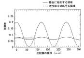
しかしながら、このように反射膜を例えば酸化アルミニウムまたは酸化ケイ素により構成すると、発振波長における反射膜の屈折率は、窒化物系III−V族化合物半導体層に対してと同じように基板の屈折率よりも小さくなってしまう。よって、図3に示したように、反射膜の膜厚を窒化物系III−V族化合物半導体層に対応する領域での反射率が低くなるように調節すると、基板に対応する領域での反射率も低くなってしまう。なお、図3は、サファイアよりなる基板の上に窒化物系III−V族化合物半導体層を積層し、酸化アルミニウムよりなる反射膜を形成した半導体レーザについて、反射膜の膜厚と波長400nmにおける反射率との関係を表したものである。図3において実線は基板に対応する領域での反射率であり、破線は発振領域での反射率である。
【0005】
しかも、サファイアよりなる基板は発振波長について透明であるので、例えば、半導体レーザをパッケージ内に収納して用いる場合、パッケージ内で反射された迷光が基板に対応する反射膜の領域からも半導体レーザ内に進入してしまう。よって、それによりノイズが発生し、特性が悪化してしまうという問題があった。
【0006】
本発明はかかる問題点に鑑みてなされたもので、その目的は、射出側の反射膜において基板に対応する領域から迷光が進入することを抑制し、特性を改善することができる半導体レーザを提供することにある。
【0007】
【課題を解決するための手段】
本発明による半導体レーザは、発振波長に対して透明な基板と、この基板に積層された半導体層とを備えると共に、その積層方向に対して垂直な方向に対向する一対の共振器端面を有するものであって、一方の共振器端面に、半導体層および基板に対応して射出側の反射膜を有し、この反射膜は、その屈折率がレーザ光の発振波長において実効屈折率と前記基板の屈折率との間の中間付近の値であり、かつ、その膜厚がレーザ光の発振領域での反射率が極小値となり、基板に対応する領域での反射率が極大値となる値に設定されているものである。
【0008】
本発明による半導体レーザでは、射出側の反射膜は、その屈折率がレーザ光の発振波長において実効屈折率と基板の屈折率との間の中間付近の値であり、かつ、その膜厚がレーザ光の発振領域での反射率が極小値、基板に対応する領域での反射率が極大値となるように設定されているので、基板に対応する領域での反射率が特に高くなり、反射膜の基板に対応する領域からの迷光の内部への進入を減少させることができる。
【0009】
【発明の実施の形態】
以下、本発明の実施の形態について、図面を参照して詳細に説明する。
【0010】
図1は本発明の一実施の形態に係る半導体レーザの構成を表すものである。この半導体レーザは、基板11の一面側に、短周期型周期律表における3B族元素のうちの少なくとも1種と5B族元素のうちの少なくとも窒素(N)とを含む窒化物系III−V族化合物半導体よりなる半導体層20を備えている。この半導体層20は、例えば、基板11の側から順に積層されたバッファ層21,n側コンタクト層22,n型クラッド層23,n型ガイド層24,活性層25,p型ガイド層26,p型クラッド層27およびp側コンタクト層28を有している。このうちn側コンタクト層22,n型クラッド層23およびn型ガイド層24は第1導電型半導体層に対応するn型半導体層であり、p型ガイド層26,p型クラッド層27およびp側コンタクト層28は第2導電型半導体層に対応するp型半導体層である。
【0011】
基板11は、例えば、積層方向における厚さ(以下、単に厚さという)が90μmのサファイアにより構成されており、半導体層20は基板11のc面に形成されている。
【0012】
バッファ層21は、例えば、厚さが30nmであり、不純物を添加しないundope−GaNにより構成されている。n側コンタクト層22は、例えば、厚さが3μmであり、n型不純物としてケイ素(Si)を添加したn型GaNにより構成されている。n型クラッド層23は、例えば、厚さが1μmであり、n型不純物としてケイ素を添加したn型AlGaN混晶により構成されている。n型ガイド層24は、例えば、厚さが0.1μmであり、n型不純物としてケイ素を添加したn型GaNにより構成されている。
【0013】
活性層25は、例えば、厚さが30nmであり、組成の異なるGaxIn1-xN(但し、1≧x≧0)混晶層を積層した多重量子井戸構造を有している。この活性層25は、少なくともその一部が発光部として機能するものであり、その発光波長は例えば400nm前後である。
【0014】
p型ガイド層26は、例えば、厚さが0.1μmであり、p型不純物としてマグネシウム(Mg)を添加したp型GaNにより構成されている。p型クラッド層27は、例えば、厚さが0.8μmであり、p型不純物としてマグネシウムを添加したp型AlGaN混晶により構成されている。p側コンタクト層28は、例えば、厚さが0.5μmであり、p型不純物としてマグネシウムを添加したp型GaNにより構成されている。p側コンタクト層28およびp型クラッド層27の一部は、半導体層20の積層方向に対して垂直な共振器方向Aに延長された細い帯状とされている。これにより、この半導体レーザでは電流狭窄を行い、活性層25のうちp側コンタクト層28に対応する領域が発光部として機能するようになっている。
【0015】
また、この半導体レーザは、共振器方向Aに対して垂直な方向におけるn側コンタクト層22の幅が、n型クラッド層23,n型ガイド層24,活性層25,p型ガイド層26,p型クラッド層27およびp側コンタクト層28の幅よりも広くなっており、n側コンタクト層22の一部にこれらn型クラッド層23,n型ガイド層24,活性層25,p型ガイド層26,p型クラッド層27およびp側コンタクト層28が積層されている。
【0016】
n側コンタクト層22からp側コンタクト層28の表面には、例えば二酸化ケイ素よりなる絶縁膜31が形成されている。この絶縁膜31にはn側コンタクト層22およびp側コンタクト層28に対応して開口がそれぞれ設けられており、n側コンタクト層22およびp側コンタクト層28の上には、これらの開口に対応してn側電極32およびp側電極33がそれぞれ形成されている。n側電極32は、例えばチタン(Ti)およびアルミニウム(Al)を順次積層して熱処理により合金化した構造を有しており、n側コンタクト層22と電気的に接続されている。p側電極33は、例えばパラジウム(Pd),白金(Pt)および金(Au)が順次積層された構造を有しており、p側コンタクト層28と電気的に接続されている。
【0017】
更に、この半導体レーザは、共振器方向Aに対向する一対の共振器端面41,42を半導体層20および基板11に対応して有している。このうち一方の共振器端面41には例えば射出側の反射膜43が形成され、他方の共振器端面42には非射出側の反射膜44が形成されている。反射膜43はレーザ光の発振領域での発振波長における反射率が低くなるように調節され、反射膜44はその反射率が高くなるように調節されている。これにより、活性層25およびその近傍において発生した光がそれら反射膜43,44の間において増幅され、レーザ光が反射膜43の側から主として射出されるようになっている。なお、反射膜44の方からも反射膜43の側に比べれば少ないもののその反射率に応じてレーザ光が射出されるが、本明細書においては、レーザ光を主として取り出す方を射出側と言い、他方を非射出側と言う。
【0018】
反射膜43は、例えば、窒化アルミニウム(AlN),酸化ジルコニウム(ZrO2)または酸化窒化ケイ素(SiOxNy)のうちの少なくとも1種を含んで構成されている。この反射膜43は、レーザ光の発振波長(例えば400nm)において屈折率が基板11の屈折率と実効屈折率との間の値となっている。なお、実効屈折率というのは、レーザ光の発振領域における平均的な屈折率を言う。また、レーザの発振領域というのは主として活性層25であるが、その近傍の領域、例えばn型ガイド層24およびp型ガイド層26、更にはn型クラッド層23の一部およびp型クラッド層27の一部なども含まれる。
【0019】
本実施の形態では、例えば、波長400nmにおける基板11の屈折率が1.77であり、実効屈折率が2.5であるので、反射膜43の屈折率は、基板11の屈折率よりも大きく、実効屈折率よりも小さい値を有している。なお、上述した材料の波長400nmにおける屈折率は、窒化アルミニウムが2.13、酸化ジルコニウムが2.07であり、酸化窒化ケイ素は酸素(O)と窒素(N)との組成比に応じて1.5〜2.07の間で任意の値を有する。
【0020】
反射膜43の屈折率をこのように規定するのは、反射膜43の膜厚をレーザ光の発振領域での反射率が低くなるように調節した場合に、基板11に対応する領域での反射率を高くすることができ、迷光の進入を抑制することができるからである。特に、反射膜43の屈折率を基板11の屈折率と実効屈折率との中間付近の値とすれば、レーザ光の発振領域での反射率が極小値となる時に、基板11に対応する領域での反射率をほぼ極大値とすることができるので好ましい。
【0021】
図2は、反射膜43の膜厚と波長400nmにおける反射率との関係を表すものである。これは、本実施の形態に係る半導体レーザについて反射膜43を窒化アルミニウムの単層膜により構成した場合のものである。図2において実線は基板11に対応する反射膜43の領域での反射率であり、破線はレーザ光の発振領域に対応する反射膜43の領域での反射率である。
【0022】
このように、反射膜43の屈折率を基板11の屈折率と実効屈折率との間の値とすると、反射膜43の膜厚と反射率との関係は、基板11に対応する領域とレーザ光の発振領域とでほぼ反対になる。よって、レーザ光の発振領域での反射率を例えば8%程度とすると、基板11に対応する領域での反射率は約20%と大きくなる。これに対して、従来の図3に示した例では、同じくレーザ光の発振領域での反射率を8%程度とすると、基板11に対応する領域での反射率は約7%と小さい。すなわち、本実施の形態によれば、基板11に対応する反射膜43の領域での反射率は従来の3倍近くにもなり、その領域から進入する迷光の影響は従来の約1/3となる。
【0023】
なお、反射膜43は単層構造でも多層構造でもよいが、単層構造の方が成膜が簡便であるので好ましい。反射膜43の厚さは、例えば、反射膜43の屈折率をn、光学的厚さをL、発振波長をλとすると、λ/4nであることが好ましい。
【0024】
また、反射膜43を構成する材料としては、特に窒化アルミニウムが好ましい。本実施の形態においては反射膜43の屈折率を基板11の屈折率と実効屈折率とのほぼ中間とすることができると共に、熱膨張係数が半導体層20と近いので、共振器端面41にかかる応力を低減させることができ、劣化を抑制することができるからである。また、熱伝導率が高いので、共振器端面41における温度の上昇を抑制することもでき、更に、酸化物あるいは酸素が共振器端面41に接触しないので、共振器端面41の酸化による光学損傷(Catastrophic Optical Damage ;COD)を防止することもできるからである。
【0025】
一方、反射膜44は、例えば、酸化ケイ素膜と酸化チタン(TiO2)膜とが交互に積層された多層構造(例えば6層)とされている。
【0026】
この半導体レーザは、例えば次のようにして製造することができる。
【0027】
まず、例えば、厚さ400μm程度のサファイアよりなる基板11を用意し、基板11のc面に、MOCVD法により、undope−GaNよりなるバッファ層21,n型GaNよりなるn側コンタクト層22,n型AlGaN混晶よりなるn型クラッド層23,n型GaNよりなるn型ガイド層24,GaInN混晶よりなる活性層25,p型GaNよりなるp型ガイド層26,p型AlGaN混晶よりなるp型クラッド層27およびp型GaNよりなるp側コンタクト層28を順次成長させる。
【0028】
なお、MOCVDを行う際、ガリウムの原料ガスとしては例えばトリメチルガリウム((CH3)3Ga)、アルミニウムの原料ガスとしては例えばトリメチルアルミニウム((CH3)3Al)、インジウムの原料ガスとしては例えばトリメチルインジウム((CH3)3In)、窒素の原料ガスとしては例えばアンモニア(NH3)をそれぞれ用いる。また、ケイ素の原料ガスとしては例えばモノシラン(SiH4)を用い、マグネシウムの原料ガスとしては例えばビス=シクロペンタジエニルマグネシウム((C5H5)2Mg)を用いる。
【0029】
次いで、p側コンタクト層28,p型クラッド層27,p型ガイド層26,活性層25,n型ガイド層24,n型クラッド層23およびn側コンタクト層22の一部を順次エッチングして、n側コンタクト層22を表面に露出させる。続いて、p側コンタクト層28の上に図示しないマスクを形成し、このマスクを利用してp側コンタクト層28およびp型クラッド層27の一部を選択的にエッチングして、p型クラッド層27の上部およびp側コンタクト層28を細い帯状とする。
【0030】
そののち、露出面全体に、例えば蒸着法により酸化ケイ素よりなる絶縁層31を形成し、p側コンタクト層28に対応して開口を設け、p側コンタクト層28を表面に露出させる。p側コンタクト層28を露出させたのち、絶縁層31のn側コンタクト層22上の領域に開口を形成し、この開口に対応して、例えば、チタン(Ti),アルミニウム(Al),白金および金を順次蒸着し、合金化してn側電極32を形成する。また、露出させたp側コンタクト層28に対応して、例えばパラジウム,白金および金を順次蒸着し、p側電極33を形成する。
【0031】
次いで、基板11を例えば90μm程度の厚さとなるように研磨する。基板11を研磨したのち、基板11を共振器方向Aに対して垂直に所定の幅で分割し、共振器端面41,42を形成する。そののち、例えばECR(Electron Cycrotron Resonance;電子サイクロトロン共鳴)スパッタ装置を用い、共振器端面41に反射膜43を形成すると共に、共振器端面42に反射膜44を形成する。反射膜43,44を形成したのち、基板11を共振器方向Aに対して平行に所定の位置で分割する。これにより、図1に示した半導体レーザが完成する。
【0032】
この半導体レーザは、次のように作用する。
【0033】
この半導体レーザでは、n側電極32とp側電極33との間に所定の電圧が印加されると、活性層25に電流が注入され、電子−正孔再結合により発光が起こる。この光は、反射膜43,44の間で反射され、増幅されてレーザ発振を生じ、主として反射膜43を透過してレーザ光として外部に射出される。例えば、半導体レーザをパッケージ内に収納して用いる場合、射出されたレーザ光の一部はパッケージ内において反射され、迷光となって半導体レーザに戻ってくる。ここでは、反射膜43の発振波長における屈折率が基板11の屈折率と実効屈折率との間の値となっており、基板11に対応する反射膜43の領域での反射率が高くなっている。よって、基板11に対応する反射膜43の領域から進入する迷光が減少し、ノイズの発生が抑制され、出力変動などの特性が改善される。
【0034】
このように本実施の形態に係る半導体レーザによれば、発振波長において反射膜43の屈折率が基板11の屈折率と実効屈折率との間の値となるようにしたので、基板11に対応する反射膜43の領域での反射率を高くすることができ、迷光の進入を抑制することができる。よって、ノイズの発生を防止でき、特性を改善することができる。
【0035】
特に、反射膜43を窒化アルミニウムにより構成すれば、基板11に対応する反射膜43の領域での反射率を特に高くすることができると共に、反射膜41側における共振器端面の劣化を抑制することができ、更にその近傍における光学損傷も防止することができる。
【0036】
以上、実施の形態を挙げて本発明を説明したが、本発明は上記実施の形態に限定されるものではなく、種々変形可能である。例えば、上記実施の形態では、反射膜43を構成する材料について具体例を挙げて説明したが、発振波長において基板11の屈折率と実効屈折率との間の屈折率を有し、レーザ光を吸収しない材料であれば、他の材料により構成するようにしてもよい。
【0037】
また、上記実施の形態では、基板11をサファイアにより構成するようにしたが、他の材料により構成するようにしてもよい。
【0038】
更に、上記実施の形態では、窒化物系III−V族化合物半導体よりなる半導体層20を備える場合について説明したが、本発明は、III−V族化合物半導体またはII−VI族化合物半導体などの他の半導体材料を用いた半導体レーザについても適用することができる。
【0039】
加えて、上記実施の形態では、発振波長における反射膜43の屈折率が基板11の屈折率よりも大きく、実効屈折率よりも小さい場合について説明したが、反射膜の屈折率が基板の屈折率よりも小さく、実効屈折率よりも大きい場合であっても同様の効果が得られる。
【0040】
更にまた、上記実施の形態では、n側コンタクト層22,n型クラッド層23,n型ガイド層24,活性層25,p型ガイド層26,p型クラッド層27およびp側コンタクト層28を順次積層するようにしたが、本発明は、他の構造を有する半導体レーザについても同様に適用することができる。例えば、n型ガイド層24およびp型ガイド層26を備えていなくてもよく、活性層25とp型ガイド層26との間に結晶劣化防止層を備えていてもよい。また、p側コンタクト層28を細い帯状とすること以外の他の構造により電流狭窄するようにしてもよい。更に、屈折率導波型あるいは利得導波型の半導体レーザとしてもよい。
【0041】
加えてまた、上記実施の形態では、n型半導体層が第1導電型半導体層に対応し、p型半導体層が第2導電型半導体層に対応する場合について説明したが、本発明には、p型半導体層が第1導電型半導体層に対応し、n型半導体層が第2導電型半導体層に対応する場合も含まれる。
【0042】
更にまた、上記実施の形態では、他方の共振器端面42に非射出側の反射膜44を備える場合について説明したが、他の構成を有する反射膜を備えていてもよく、また反射膜が設けられていなくてもよい。
【0043】
【発明の効果】
以上説明したように請求項1ないし請求項4のいずれか1項に記載の半導体レーザによれば、射出側の反射膜の、レーザ光の発振波長における屈折率を実効屈折率と基板の屈折率との間の中間付近の値とし、かつ、その膜厚を、レーザ光の発振領域での反射率が極小値となるときに、基板に対応する領域での反射率が極大値となるように設定したので、基板に対応する反射膜の領域での反射率を特に高くすることができ、迷光の進入を抑制することができる。よって、ノイズの発生を防止でき、特性を改善することができるという効果を奏する。
【図面の簡単な説明】
【図1】本発明の一実施の形態に係る半導体レーザの構成を表す部分分解斜視図である。
【図2】図1に示した半導体レーザにおける反射膜の膜厚と反射率との関係を表す特性図である。
【図3】従来の半導体レーザにおける反射膜の膜厚と反射率との関係を表す特性図である。
【符号の説明】
11…基板、20…半導体層、21…バッファ層、22…n側コンタクト層、23…n型クラッド層、24…n型ガイド層、25…活性層、26…p型ガイド層、27…p型クラッド層、28…p側コンタクト層、31…絶縁膜、32…n側電極、33…p側電極、41,42…共振器端面、43…反射膜(射出側)、44…反射膜(非射出側)、A…共振器方向[0001]
BACKGROUND OF THE INVENTION
The present invention relates to a semiconductor laser in which a semiconductor layer is stacked on a substrate and a pair of resonator end faces facing each other in a direction perpendicular to the stacking direction is provided.
[0002]
[Prior art]
In recent years, a semiconductor laser (laser diode; LD) has been used in various optical devices. A semiconductor laser generally has a structure in which a first conductive type semiconductor layer, an active layer, and a second conductive type semiconductor layer are sequentially stacked on a substrate. For example, light generated in the active layer is perpendicular to the stacking direction. Amplification is performed between a pair of resonator end faces facing each other in any direction. In many cases, the pair of resonator end faces are each provided with a reflection film for adjusting the reflectivity and protecting the end face of the resonator. Of these, the reflective film on the side from which the laser light is mainly emitted is adjusted so that the reflectance is low, and the reflective film on the other non-emission side is adjusted so that the reflectance is high.
[0003]
These reflective films have a single-layer structure or a multilayer structure depending on the application, but the reflective film on the exit side is often a single-layer structure because the film formation is simple. For example, in a semiconductor laser in which a nitride III-V compound semiconductor layer is stacked on a substrate made of sapphire, the reflection film on the emission side is oxidized with a smaller refractive index at the oscillation wavelength than the nitride III-V compound semiconductor. A single layer structure of aluminum (Al2 O3 ) or silicon oxide (SiO2 ) is generally used.
[0004]
[Problems to be solved by the invention]
However, when the reflective film is made of, for example, aluminum oxide or silicon oxide, the refractive index of the reflective film at the oscillation wavelength is less than the refractive index of the substrate in the same manner as the nitride III-V compound semiconductor layer. Will also get smaller. Therefore, as shown in FIG. 3, when the thickness of the reflective film is adjusted so that the reflectance in the region corresponding to the nitride-based III-V compound semiconductor layer is lowered, the reflection in the region corresponding to the substrate is reflected. The rate will also be low. FIG. 3 shows a reflection of a semiconductor film in which a nitride III-V compound semiconductor layer is laminated on a substrate made of sapphire and a reflective film made of aluminum oxide is formed, and the reflection at a wavelength of 400 nm. It represents the relationship with the rate. In FIG. 3, the solid line is the reflectance in the region corresponding to the substrate, and the broken line is the reflectance in the oscillation region.
[0005]
In addition, since the substrate made of sapphire is transparent with respect to the oscillation wavelength, for example, when a semiconductor laser is housed in a package, stray light reflected in the package is also reflected in the semiconductor laser from the region of the reflective film corresponding to the substrate. I will enter. Therefore, there is a problem that noise is generated and characteristics are deteriorated.
[0006]
The present invention has been made in view of such problems, and an object thereof is to provide a semiconductor laser capable of improving the characteristics by suppressing stray light from entering from a region corresponding to the substrate in the reflection film on the emission side. There is to do.
[0007]
[Means for Solving the Problems]
A semiconductor laser according to the present invention includesa substratetransparent to an oscillation wavelength and a semiconductor layer laminated on the substrate, and has a pair of resonator end faces facing in a direction perpendicular to the lamination direction. a is, the one resonator endface, the semiconductor layer and has a reflection film on the exit sidecorresponds to the substrate, the reflectionfilm, a refractive index of the substrate and the effective refractive index in the oscillation wavelength of the laser beamIt is a value in themiddle of the refractive index, and the film thickness is set to a value at which the reflectance in the laser light oscillation region is a minimum value and the reflectance in the region corresponding to the substrate is a maximum value. It is what has been.
[0008]
In the semiconductor laser according to the present invention,the reflection film on the emission side has a refractive index that is a value near the middle between the effective refractive index and the refractive index of the substrate at the oscillation wavelength of the laser beam, and the film thickness thereof is the laser. Since the reflectance in the light oscillation region is set to the minimum value and the reflectance in the region corresponding to the substrate is set to the maximum value, the reflectance in the region corresponding to the substrate is particularly high, and the reflection film Intrusion of stray light from the region corresponding to the substrate can be reduced.
[0009]
DETAILED DESCRIPTION OF THE INVENTION
Hereinafter, embodiments of the present invention will be described in detail with reference to the drawings.
[0010]
FIG. 1 shows a configuration of a semiconductor laser according to an embodiment of the present invention. This semiconductor laser includes a nitride III-V group containing at least one of group 3B elements and at least nitrogen (N) of group 5B elements on one surface side of
[0011]
The
[0012]
The
[0013]
The
[0014]
The p-
[0015]
Further, in this semiconductor laser, the width of the n-
[0016]
An insulating
[0017]
Further, the semiconductor laser has a pair of resonator end faces 41 and 42 facing the resonator direction A corresponding to the
[0018]
The
[0019]
In the present embodiment, for example, the refractive index of the
[0020]
The refractive index of the
[0021]
FIG. 2 shows the relationship between the film thickness of the
[0022]
As described above, when the refractive index of the
[0023]
The
[0024]
In addition, as a material constituting the
[0025]
On the other hand, the
[0026]
This semiconductor laser can be manufactured, for example, as follows.
[0027]
First, for example, a
[0028]
When performing MOCVD, for example, trimethylgallium ((CH3 )3 Ga) is used as a gallium source gas, trimethylaluminum ((CH3 )3 Al) is used as an aluminum source gas, and indium source gas is used as an example. For example, ammonia (NH3 ) is used as a source gas for trimethylindium ((CH3 )3 In) and nitrogen, respectively. For example, monosilane (SiH4 ) is used as the silicon source gas, and bis = cyclopentadienyl magnesium ((C5 H5 )2 Mg) is used as the magnesium source gas.
[0029]
Next, the p-
[0030]
After that, an insulating
[0031]
Next, the
[0032]
This semiconductor laser operates as follows.
[0033]
In this semiconductor laser, when a predetermined voltage is applied between the n-
[0034]
As described above, according to the semiconductor laser according to the present embodiment, the refractive index of the
[0035]
In particular, if the
[0036]
Although the present invention has been described with reference to the embodiment, the present invention is not limited to the above embodiment, and various modifications can be made. For example, in the above-described embodiment, the material constituting the
[0037]
Moreover, in the said embodiment, although the board |
[0038]
Furthermore, in the above-described embodiment, the case where the
[0039]
In addition, in the above-described embodiment, the case where the refractive index of the
[0040]
Furthermore, in the above embodiment, the n-
[0041]
In addition, in the above embodiment, the case where the n-type semiconductor layer corresponds to the first conductivity type semiconductor layer and the p-type semiconductor layer corresponds to the second conductivity type semiconductor layer has been described. The case where the p-type semiconductor layer corresponds to the first conductivity type semiconductor layer and the n-type semiconductor layer corresponds to the second conductivity type semiconductor layer is also included.
[0042]
Furthermore, in the above embodiment, the case where the other resonator end face 42 is provided with the
[0043]
【The invention's effect】
As described above, according to the semiconductor laser of any one of
[Brief description of the drawings]
FIG. 1 is a partially exploded perspective view showing a configuration of a semiconductor laser according to an embodiment of the present invention.
2 is a characteristic diagram showing the relationship between the thickness of a reflective film and the reflectance in the semiconductor laser shown in FIG.
FIG. 3 is a characteristic diagram showing the relationship between the thickness of a reflective film and the reflectance in a conventional semiconductor laser.
[Explanation of symbols]
DESCRIPTION OF
Claims (4)
Translated fromJapanese前記一方の共振器端面に、前記半導体層および基板に対応して射出側の反射膜を有し、この反射膜は、その屈折率がレーザ光の発振波長において実効屈折率と前記基板の屈折率との間の中間付近の値であり、かつ、その膜厚がレーザ光の発振領域での反射率が極小値となり、前記基板に対応する領域での反射率が極大値となる値に設定されている
ことを特徴とする半導体レーザ。A semiconductor laser comprisinga substratetransparent to an oscillation wavelength and a semiconductor layer laminated on the substrate, and having a pair of resonator end faces facing in a direction perpendicular to the lamination direction,
Said one resonator end face ofsaid semiconductor layer and has a reflection film on the exit sidecorresponds to the substrate, the reflectivefilm, the refractive index of the substrate and the effective refractive indexwhose refractive index is at the oscillation wavelength of the laser beam And thefilm thickness is set to a value at which the reflectance in the laser light oscillation region is a minimum value and the reflectance in the region corresponding to the substrate is a maximum value. a semiconductor laser, characterized bythat.
Priority Applications (3)
| Application Number | Priority Date | Filing Date | Title |
|---|---|---|---|
| JP2000207229AJP3646302B2 (en) | 2000-07-07 | 2000-07-07 | Semiconductor laser |
| US09/883,235US6693935B2 (en) | 2000-06-20 | 2001-06-19 | Semiconductor laser |
| US10/720,112US7065118B2 (en) | 2000-06-20 | 2003-11-25 | Semiconductor laser |
Applications Claiming Priority (1)
| Application Number | Priority Date | Filing Date | Title |
|---|---|---|---|
| JP2000207229AJP3646302B2 (en) | 2000-07-07 | 2000-07-07 | Semiconductor laser |
Publications (2)
| Publication Number | Publication Date |
|---|---|
| JP2002026442A JP2002026442A (en) | 2002-01-25 |
| JP3646302B2true JP3646302B2 (en) | 2005-05-11 |
Family
ID=18704028
Family Applications (1)
| Application Number | Title | Priority Date | Filing Date |
|---|---|---|---|
| JP2000207229AExpired - Fee RelatedJP3646302B2 (en) | 2000-06-20 | 2000-07-07 | Semiconductor laser |
Country Status (1)
| Country | Link |
|---|---|
| JP (1) | JP3646302B2 (en) |
Families Citing this family (9)
| Publication number | Priority date | Publication date | Assignee | Title |
|---|---|---|---|---|
| JP4383172B2 (en) | 2001-10-26 | 2009-12-16 | アンモノ・スプウカ・ジ・オグラニチョノン・オドポヴィエドニアウノシツィオン | Light emitting device structure using nitride bulk single crystal layer and manufacturing method thereof |
| JP4416648B2 (en) | 2002-05-17 | 2010-02-17 | アンモノ・スプウカ・ジ・オグラニチョノン・オドポヴィエドニアウノシツィオン | Method for manufacturing light emitting device |
| US20060138431A1 (en) | 2002-05-17 | 2006-06-29 | Robert Dwilinski | Light emitting device structure having nitride bulk single crystal layer |
| PL216522B1 (en) | 2002-06-26 | 2014-04-30 | Ammono Spółka Z Ograniczoną Odpowiedzialnością | Nitride semiconductor laser device and a method for improving its performance |
| KR101088991B1 (en) | 2002-12-11 | 2011-12-01 | 니치아 카가쿠 고교 가부시키가이샤 | Process for producing bulk monocrystalline gallium-containing nitride |
| JP5285835B2 (en) | 2005-07-13 | 2013-09-11 | 株式会社東芝 | Semiconductor device and manufacturing method thereof |
| JP4514760B2 (en) | 2007-01-26 | 2010-07-28 | シャープ株式会社 | Semiconductor laser element |
| JP2009231367A (en)* | 2008-03-19 | 2009-10-08 | Sharp Corp | Nitride semiconductor laser element and external resonator type semiconductor laser device |
| JP2012069970A (en)* | 2011-11-01 | 2012-04-05 | Toshiba Corp | Semiconductor device |
- 2000
- 2000-07-07JPJP2000207229Apatent/JP3646302B2/ennot_activeExpired - Fee Related
Also Published As
| Publication number | Publication date |
|---|---|
| JP2002026442A (en) | 2002-01-25 |
Similar Documents
| Publication | Publication Date | Title |
|---|---|---|
| US6693935B2 (en) | Semiconductor laser | |
| JP5285835B2 (en) | Semiconductor device and manufacturing method thereof | |
| JP3220977B2 (en) | A nitride semiconductor laser device and a method for manufacturing a nitride semiconductor laser device. | |
| JPWO2002101894A1 (en) | Semiconductor laser device | |
| JP2820140B2 (en) | Gallium nitride based semiconductor laser | |
| JP3646302B2 (en) | Semiconductor laser | |
| JP2002237648A (en) | Semiconductor laser element | |
| US20100014550A1 (en) | Nitride semiconductor laser device | |
| JPH1168256A (en) | Nitride semiconductor laser device | |
| JP2003163417A (en) | Semiconductor light emitting device and method of manufacturing the same | |
| JPH1117248A (en) | Highly reflective film structure for semiconductor laser and semiconductor laser | |
| JP3212008B2 (en) | Gallium nitride based compound semiconductor laser device | |
| JP3880683B2 (en) | Method for manufacturing gallium nitride based semiconductor light emitting device | |
| JP4457417B2 (en) | Nitride semiconductor laser device | |
| JP2003031894A (en) | Semiconductor laser and its manufacturing method | |
| JP3264163B2 (en) | Nitride semiconductor laser device | |
| JP3502527B2 (en) | Nitride semiconductor laser device | |
| JP2010034221A (en) | Edge-emitting semiconductor laser and manufacturing method thereof | |
| JP2006228826A (en) | Semiconductor laser | |
| JP2002043692A (en) | Semiconductor laser and its manufacturing method | |
| JP2000216476A (en) | Semiconductor light emitting element | |
| JP4045792B2 (en) | Nitride semiconductor laser device | |
| JP3101997B2 (en) | Nitride semiconductor laser device | |
| JP2004111997A (en) | Semiconductor laser device | |
| JP3307218B2 (en) | Method for manufacturing nitride semiconductor laser device |
Legal Events
| Date | Code | Title | Description |
|---|---|---|---|
| A131 | Notification of reasons for refusal | Free format text:JAPANESE INTERMEDIATE CODE: A131 Effective date:20040427 | |
| A521 | Written amendment | Free format text:JAPANESE INTERMEDIATE CODE: A523 Effective date:20040628 | |
| A521 | Written amendment | Free format text:JAPANESE INTERMEDIATE CODE: A821 Effective date:20040628 | |
| TRDD | Decision of grant or rejection written | ||
| A01 | Written decision to grant a patent or to grant a registration (utility model) | Free format text:JAPANESE INTERMEDIATE CODE: A01 Effective date:20050117 | |
| A61 | First payment of annual fees (during grant procedure) | Free format text:JAPANESE INTERMEDIATE CODE: A61 Effective date:20050130 | |
| FPAY | Renewal fee payment (event date is renewal date of database) | Free format text:PAYMENT UNTIL: 20080218 Year of fee payment:3 | |
| FPAY | Renewal fee payment (event date is renewal date of database) | Free format text:PAYMENT UNTIL: 20090218 Year of fee payment:4 | |
| FPAY | Renewal fee payment (event date is renewal date of database) | Free format text:PAYMENT UNTIL: 20100218 Year of fee payment:5 | |
| LAPS | Cancellation because of no payment of annual fees |