JP3639767B2 - Surface mount antenna and communication device using the same - Google Patents
Surface mount antenna and communication device using the sameDownload PDFInfo
- Publication number
- JP3639767B2 JP3639767B2JP2000111820AJP2000111820AJP3639767B2JP 3639767 B2JP3639767 B2JP 3639767B2JP 2000111820 AJP2000111820 AJP 2000111820AJP 2000111820 AJP2000111820 AJP 2000111820AJP 3639767 B2JP3639767 B2JP 3639767B2
- Authority
- JP
- Japan
- Prior art keywords
- radiation electrode
- electrode
- dielectric substrate
- mount antenna
- parasitic
- Prior art date
- Legal status (The legal status is an assumption and is not a legal conclusion. Google has not performed a legal analysis and makes no representation as to the accuracy of the status listed.)
- Expired - Fee Related
Links
- 238000004891communicationMethods0.000titleclaimsdescription20
- 230000005855radiationEffects0.000claimsdescription168
- 230000003071parasitic effectEffects0.000claimsdescription73
- 239000000758substrateSubstances0.000claimsdescription70
- 239000011295pitchSubstances0.000description41
- 238000010586diagramMethods0.000description15
- 230000005284excitationEffects0.000description12
- 239000004020conductorSubstances0.000description7
- 230000008878couplingEffects0.000description5
- 238000010168coupling processMethods0.000description5
- 238000005859coupling reactionMethods0.000description5
- 230000000694effectsEffects0.000description5
- 230000002411adverseEffects0.000description3
- 230000006866deteriorationEffects0.000description3
- 239000003990capacitorSubstances0.000description2
- 230000005540biological transmissionEffects0.000description1
- 230000005684electric fieldEffects0.000description1
- 238000004519manufacturing processMethods0.000description1
- 238000000034methodMethods0.000description1
Images


Classifications
- H—ELECTRICITY
- H01—ELECTRIC ELEMENTS
- H01Q—ANTENNAS, i.e. RADIO AERIALS
- H01Q1/00—Details of, or arrangements associated with, antennas
- H01Q1/12—Supports; Mounting means
- H01Q1/22—Supports; Mounting means by structural association with other equipment or articles
- H01Q1/2283—Supports; Mounting means by structural association with other equipment or articles mounted in or on the surface of a semiconductor substrate as a chip-type antenna or integrated with other components into an IC package
- H—ELECTRICITY
- H01—ELECTRIC ELEMENTS
- H01Q—ANTENNAS, i.e. RADIO AERIALS
- H01Q1/00—Details of, or arrangements associated with, antennas
- H01Q1/12—Supports; Mounting means
- H01Q1/22—Supports; Mounting means by structural association with other equipment or articles
- H01Q1/24—Supports; Mounting means by structural association with other equipment or articles with receiving set
- H01Q1/241—Supports; Mounting means by structural association with other equipment or articles with receiving set used in mobile communications, e.g. GSM
- H01Q1/242—Supports; Mounting means by structural association with other equipment or articles with receiving set used in mobile communications, e.g. GSM specially adapted for hand-held use
- H01Q1/243—Supports; Mounting means by structural association with other equipment or articles with receiving set used in mobile communications, e.g. GSM specially adapted for hand-held use with built-in antennas
- H—ELECTRICITY
- H01—ELECTRIC ELEMENTS
- H01Q—ANTENNAS, i.e. RADIO AERIALS
- H01Q1/00—Details of, or arrangements associated with, antennas
- H01Q1/36—Structural form of radiating elements, e.g. cone, spiral, umbrella; Particular materials used therewith
- H—ELECTRICITY
- H01—ELECTRIC ELEMENTS
- H01Q—ANTENNAS, i.e. RADIO AERIALS
- H01Q1/00—Details of, or arrangements associated with, antennas
- H01Q1/36—Structural form of radiating elements, e.g. cone, spiral, umbrella; Particular materials used therewith
- H01Q1/38—Structural form of radiating elements, e.g. cone, spiral, umbrella; Particular materials used therewith formed by a conductive layer on an insulating support
- H—ELECTRICITY
- H01—ELECTRIC ELEMENTS
- H01Q—ANTENNAS, i.e. RADIO AERIALS
- H01Q21/00—Antenna arrays or systems
- H01Q21/28—Combinations of substantially independent non-interacting antenna units or systems
- H—ELECTRICITY
- H01—ELECTRIC ELEMENTS
- H01Q—ANTENNAS, i.e. RADIO AERIALS
- H01Q21/00—Antenna arrays or systems
- H01Q21/29—Combinations of different interacting antenna units for giving a desired directional characteristic
- H—ELECTRICITY
- H01—ELECTRIC ELEMENTS
- H01Q—ANTENNAS, i.e. RADIO AERIALS
- H01Q5/00—Arrangements for simultaneous operation of antennas on two or more different wavebands, e.g. dual-band or multi-band arrangements
- H—ELECTRICITY
- H01—ELECTRIC ELEMENTS
- H01Q—ANTENNAS, i.e. RADIO AERIALS
- H01Q5/00—Arrangements for simultaneous operation of antennas on two or more different wavebands, e.g. dual-band or multi-band arrangements
- H01Q5/30—Arrangements for providing operation on different wavebands
- H01Q5/307—Individual or coupled radiating elements, each element being fed in an unspecified way
- H01Q5/342—Individual or coupled radiating elements, each element being fed in an unspecified way for different propagation modes
- H01Q5/357—Individual or coupled radiating elements, each element being fed in an unspecified way for different propagation modes using a single feed point
- H01Q5/364—Creating multiple current paths
- H01Q5/371—Branching current paths
- H—ELECTRICITY
- H01—ELECTRIC ELEMENTS
- H01Q—ANTENNAS, i.e. RADIO AERIALS
- H01Q5/00—Arrangements for simultaneous operation of antennas on two or more different wavebands, e.g. dual-band or multi-band arrangements
- H01Q5/30—Arrangements for providing operation on different wavebands
- H01Q5/378—Combination of fed elements with parasitic elements
Landscapes
- Engineering & Computer Science (AREA)
- Computer Networks & Wireless Communication (AREA)
- Microelectronics & Electronic Packaging (AREA)
- Details Of Aerials (AREA)
- Support Of Aerials (AREA)
- Variable-Direction Aerials And Aerial Arrays (AREA)
- Waveguide Aerials (AREA)
Description
Translated fromJapanese【0001】
【発明の属する技術分野】
本発明は、携帯型の電話機等の通信機に内蔵される表面実装型アンテナおよびそれを用いた通信機に関するものである。
【0002】
【従来の技術】
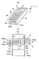
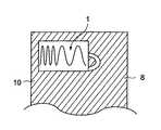
図16には携帯電話機等の通信機に内蔵される表面実装型アンテナの一例が模式的に示されている。
この表面実装型アンテナ1は誘電体基体2を有し、この誘電体基体2の表面には放射電極3と接地電極4と給電電極5が形成されている。
つまり、放射電極3は誘電体基体2の側面2aから側面2bを介し側面2cに掛けて形成されており、接地電極4は誘電体基体2の側面2dの全領域に上記放射電極3に導通して形成されている。
また、給電電極5は誘電体基体2の側面2aに放射電極3と間隔を介して形成されている。
【0003】
上記給電電極5には外部の電力供給手段(電力供給源)6が導通接続される構成であり、該電力供給手段6から給電電極5に電力が供給されると、給電電極5から放射電極3へ電力が容量結合によって供給される。
この供給電力により放射電極3が励振して表面実装型アンテナ1は予め定まる1つの周波数帯域の電波の送受信を行う。
【0004】
【発明が解決しようとする課題】
ところで、現在では、携帯型の電話機の使用周波数帯域として、900MHz帯と1.9GHz帯の2つの周波数帯域が用いられる場合がある。
【0005】
しかしながら、このような異なる2つの周波数帯域を使用することが可能な通信機には、1つのアンテナで異なる2つの周波数帯域の電波の送受信が可能な表面実装型アンテナが要求されるが、前記図16に示す表面実装型アンテナ1では、前述したように、1つの周波数帯域の電波の送受信しか行うことができなかった。
【0006】
本発明は上記課題を解決するために成されたものであり、その目的は、異なる2つ以上の周波数帯域の電波の送受信が可能な表面実装型アンテナおよびそれを用いた通信機を提供することにある。
【0007】
【課題を解決するための手段】
上記目的を達成するために、この発明は次に示す構成をもって前記課題を解決する手段としている。
すなわち、第1の発明の表面実装型アンテナは、直方体状の誘電体基体の表面に形成された放射電極によって少なくとも異なる2つの周波数帯域の電波の送受信を行う表面実装型アンテナであって、上記放射電極は第1ミアンダピッチで形成されたミアンダ状の第1電極部と、上記第1ミアンダピッチよりも狭い第2ミアンダピッチで形成されたミアンダ状の第2電極部とを少なくとも有し、上記放射電極は上記第1電極部と上記第2電極部が直列に接続されたミアンダ状の放射電極と成し、上記放射電極は上記第1電極部と上記第2電極部とが共に共振する周波数帯域と、該周波数帯域よりも周波数が高い上記第2電極部が単独で共振する周波数帯域とにおいて電波の送受信を行なう構成と成して、上記放射電極は上記誘電体基体の表面の内の2面以上に形成されており、上記誘電体基体の表面には上記放射電極に接続される給電電極が1つ形成されており、上記誘電体基体の表面には上記放射電極に電磁結合する無給電放射電極が1つ以上形成されており、該無給電放射電極は、上記放射電極が共振する複数の周波数帯域のうちの少なくとも1つの周波数帯域で複共振状態と成すことを
もって前記課題を解決する手段としている。
【0008】
第2の発明の表面実装型アンテナは、上記第1の発明の構成を備え、上記無給電放射電極はミアンダ状の無給電放射電極と成していることを特徴として構成されている。
【0009】
第3の発明の表面実装型アンテナは、上記第1又は第2の発明の構成を備え、上記無給電放射電極は上記誘電体基体の表面の2面以上の面に渡って形成されていることを特徴として構成されている。
【0010】
第4の発明の表面実装型アンテナは、上記第2又は第3の発明の構成を備え、上記無給電放射電極は上記誘電体基体の少なくとも上面に放射電極と異にした部位に形成されており、上記誘電体基体の表面の内の1つに上記放射電極と上記無給電放射電極が略直交状に形成されていることを特徴として構成されている。
【0011】
第5の発明の表面実装型アンテナは、上記第1乃至第4の発明の何れか1つの構成を備え、上記放射電極は整合回路を介して電力供給源と導通接続される構成と成し、上記整合回路は上記誘電体基体の表面に設けられていることを特徴として構成されている。
【0012】
第6の発明の表面実装型アンテナを用いた通信機は、上記第1乃至第5の発明の何れか1つの発明を構成する表面実装型アンテナが実装基板上に装着されて成ることを特徴として構成されている。
【0013】
上記構成の発明において、誘電体基体の表面に形成される放射電極は少なくともミアンダ状の第1電極部とミアンダ状の第2電極部が直列に接続されたミアンダ状の放射電極と成している。ここで、ミアンダ状の電極部はミアンダピッチおよびターン数(電気長)によって共振周波数が定まる。このことから、本発明のように、ミアンダピッチの異なる複数の電極部を直列に接続して放射電極を構成することにより、この放射電極は複数の共振周波数を有することとなる。このために、本発明の表面実装型アンテナは複数の異なる周波数帯域の電波の送受信を行うことが可能となる。また、本発明の通信機は、1つのアンテナで複数の周波数帯域をカバーできるので、小型化が可能となる。
【0014】
【発明の実施の形態】
以下に、この発明に係る実施形態例を図面に基づき説明する。
【0015】
図1(a)には第1の実施形態例における表面実装型アンテナが模式的な斜視図により示されており、図1(b)には第1の実施形態例の表面実装型アンテナを構成する誘電体基体の表面形態が展開状態で示されている。
【0016】
図1(a)、(b)に示すように、この第1の実施形態例に示す表面実装型アンテナ1は、誘電体基体2を有し、この誘電体基体2の前端面2aから上面2eを通り後端面2cに掛けてミアンダ状の放射電極3が形成されている。
【0017】
このミアンダ状の放射電極3はミアンダピッチが異なる第1電極部3aと第2電極部3bが直列に接続されて構成されている。
上記第1電極部3aのミアンダピッチ(以下、第1ミアンダピッチと記す)d1は、第2電極部3bのミアンダピッチ(以下、第2ミアンダピッチと記す)d2よりも広くなっている。
【0018】
上記第1電極部3aの第1ミアンダピッチd1およびターン数、第2電極部3bの第2ミアンダピッチd2およびターン数は次に示すように定められている。
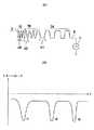
例えば、図2に示すように、第1周波数帯域f1(例えば、900MHz帯)と、該第1周波数帯域f1よりも高い第2周波数帯域f2(例えば、1.9GHz帯)との異なる2つの周波数帯域でリターンロスを低くする場合、つまり、上記周波数帯域f1,f2で電波の送受信が可能な表面実装型アンテナ1が要求される場合を例にとる。
この場合、上記第1電極部3aと第2電極部3bのうちのミアンダピッチが狭い方の第2電極部3bが図2に示す共振周波数f2を有することができるように、その第2電極部3bの第2ミアンダピッチd2およびターン数は定められる。
【0019】
また、上記第1ミアンダピッチd1と第2ミアンダピッチd2の比と、図2に示す周波数f1,f2間の間隔Hとには予め求まる相関関係がある。
このことから、この相関関係と、上述の如く定まる第2ミアンダピッチd2とに基づいて、上記第1電極部3aの第1ミアンダピッチd1が定められる。
さらに、上記第1電極部3aおよび第2電極部3bが両方共に共振周波数f1で共振することができるように、上記第1電極部3aのターン数は定められる。
なお、図1の例では、ミアンダピッチの狭い第2電極部3bは誘電体基体2の2面に渡って形成されているが、1面(2a)のみに集中させることで、上記共振周波数f1,f2のコントロールが行い易いという特徴を有する。
【0020】
図1(b)に示すように、上記誘電体基体2の後端面2cには上記放射電極3の第1電極部3aに導通接続する給電電極5が形成されている。
また、誘電体基体2の後端面2cには上記放射電極3や給電電極5と異にした部位に固定電極7aが形成されている。
【0021】
さらに、誘電体基体2の前端面2aには、放射電極3の開放端に対向する領域に固定電極7b,7cがそれぞれ形成されている。
上記給電電極5および固定電極7a,7b,7cはそれぞれ誘電体基体2の底面2fにも回り込んで形成されている。
【0022】
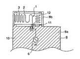
この第1の実施形態例に示す表面実装型アンテナ1は上記のように構成されており、例えば、図3に示すように、通信機の回路基板8に実装される。
すなわち、この回路基板8は、PCB等により構成されて表面に接地電極10が形成されている主要部8aと、接地電極が形成されていない非グランド部8bとを有して構成されている。
図3に示す例では、上記表面実装型アンテナ1は上記非グランド部8bに実装されている。
【0023】
上記回路基板8には上記表面実装型アンテナ1を駆動させるための電力供給源である電力供給手段6および整合回路11が設けられている。
表面実装型アンテナ1は上記非グランド部8bの所定の実装位置に表面実装されることにより、給電電極5が整合回路11を介して電力供給手段6に導通接続される。
上記電力供給手段6から整合回路11と給電電極5を順に通って電力が放射電極3に供給され、該電力に基づいて放射電極3の第1電極部3aおよび第2電極部3bが両方共に励振すると、表面実装型アンテナ1は第1周波数帯域f1での電波の送受信が可能となる。
また、上記供給電力に基づいて放射電極3の第2電極部3bのみが励振すると、表面実装型アンテナ1は前記第2周波数帯域f2での電波の送受信が可能となる。
【0024】
この第1の実施形態例によれば、放射電極3はミアンダピッチが異なる第1電極部3aと第2電極部3bが直列に接続して構成されているので、この放射電極3は異なる2つの共振周波数を有することとなる。
このことにより、この第1の実施形態例の表面実装型アンテナ1は、異なる2つの周波数帯域での電波の送受信が可能となる。
【0025】
また、この第1の実施形態例では、放射電極3は誘電体基体2の1つの面だけでなく、2つ以上の面に渡って形成される構成である。
このことから、放射電極3の形成領域が誘電体基体2の唯1つの面のみである場合よりも、放射電極3の形成領域が拡大することとなる。
このために、放射電極3の長さに大きく規制されることなく、誘電体基体2の小型化を図ることができ、表面実装型アンテナ1の設計の自由度を向上させることができる。
なお、この第1の実施形態例では、ミアンダピッチの狭い第2電極部3bは誘電体基体2の2面に渡って形成されているが、1面(2a)のみに集中させてもよい。
このように、第2電極部3bを誘電体基体2の1面のみに集中して形成する場合には、前記共振周波数f1,f2のコントロールを行い易くすることができる。
【0026】
以下に、第2の実施形態例を説明する。
なお、この第2の実施形態例の説明では、前記第1の実施形態例と同一構成部分には同一符号を付し、その共通部分の重複説明は省略する。
【0027】
前記第1の実施形態例で述べたように、表面実装型アンテナ1の放射電極3を、ミアンダピッチが異なる2つの電極部3a,3bにより構成することによって、表面実装型アンテナ1は異なる2つの周波数帯域f1,f2での電波の送受信が可能となる。
しかし、上記周波数帯域f1,f2のうちの一方の帯域幅が所望の幅よりも狭い場合がある。
【0028】
そこで、この第2の実施形態例では、上記所望の帯域幅よりも帯域幅が狭い方の周波数帯域の帯域幅を拡大するために、次に示すような構成を備えた。
図4には第2の実施形態例の表面実装型アンテナを構成する誘電体基体の表面形態が展開状態で示されている。
この第2の実施形態例では、図4に示すような無給電放射電極12が誘電体基体2に形成されていることを特徴としている。
この無給電放射電極12は誘電体基体2の上面2eに、側面2d側から側面2b側へ向かう方向にミアンダ状に形成されている。
また、誘電体基体2の底面2fから側面2dに掛けて導入パターン12aが形成されており、上記ミアンダ状の無給電放射電極12の一端側は上記導入パターン12aに導通接続され、他端側は開放端と成している。
【0029】
上記無給電放射電極12のミアンダピッチおよびターン数は次に示すように定められている。
例えば、前記周波数帯域f1,f2のうちの周波数帯域f1の帯域幅を拡大したい場合(換言すれば、広帯域化を図りたい場合)には、図5(a)に示す放射電極3の共振周波数f1から僅かにずれた周波数f1’を共振周波数として持つように、無給電放射電極12のミアンダピッチおよびターン数が定められる。
このように定められたミアンダピッチおよびターン数でもって無給電放射電極12が形成されると、前記周波数帯域f1では、放射電極3は図5(a)の実線のようなリターンロス特性を有する。
また、一方、上記無給電放射電極12は図5(a)の点線のようなリターンロス特性を有することとなる。
このことから、上記放射電極3および無給電放射電極12によって、周波数帯域f1では、図5(b)に示すような複共振状態となる。
【0030】
また、上記周波数帯域f2の帯域幅を拡大したい場合には、図5(a)に示す放射電極3の共振周波数f2から僅かにずれた周波数f2’を共振周波数として持つように、無給電放射電極12のミアンダピッチおよびターン数が定められる。
このように定められたミアンダピッチおよびターン数で無給電放射電極12が形成されると、上記同様に、周波数帯域f2では、複共振状態となる。
【0031】
図4に示すように、この第2の実施形態例では、給電電極5は、前記導入パターン12aに近接して誘電体基体2の側面2dから底面2fに掛けて形成されている。
放射電極3は、前記第1の実施形態例と同様に、ミアンダピッチが互いに異なる第1電極部3aと第2電極部3bが直列に接続されて構成されている。
そのミアンダ状の放射電極3は誘電体基体2の上面2eから側面2aに掛けて形成されている。
つまり、放射電極3のミアンダ状のパターンは前記無給電放射電極12のミアンダ状のパターンと間隔を介し、かつ、ほぼ直交状に形成されている。
この放射電極3の一端側は上記給電電極5に導通接続され、他端側は開放端と成している。
【0032】
また、図4に示すように、誘電体基体2の側面2bには固定電極7a,7bがそれぞれ間隔を介して形成され、側面2dには固定電極7c,7dがそれぞれ形成されている。
これら固定電極7a,7b,7c,7dはそれぞれ側面2bから底面2fに回り込んで形成されている。
【0033】
この第2の実施形態例に示す表面実装型アンテナ1は上記のように構成されている。
この表面実装型アンテナ1は、例えば、図6に示すように、前記第1の実施形態例と同様に回路基板8の非グランド部8bに実装される。
このように、表面実装型アンテナ1が回路基板8に実装されることにより、前記放射電極3は給電電極5と整合回路11を介して電力供給手段6に導通接続される。
また、固定電極7a,7b,7c,7dと導入パターン12aは回路基板8の接地電極10に導通接続されてグランドに接地される。
【0034】
このように表面実装型アンテナ1が実装されている状態で、上記電力供給手段6から整合回路11を通して表面実装型アンテナ1の給電電極5に電力が供給されると、その電力は給電電極5から放射電極3に供給されると共に、給電電極5から上記導入パターン12aにも電力が電磁結合によって供給される。
上記供給電力によって放射電極3が励振することによって、表面実装型アンテナ1は周波数帯域f1,f2での電波の送受信が可能となる。
また、上記供給電力に基づいて無給電放射電極12が励振すると、周波数帯域f1あるいは周波数帯域f2では複共振状態となり、これにより、帯域幅が拡大する(広帯域化が図られる)。
【0035】
この第2の実施形態例によれば、誘電体基体2の表面に無給電放射電極12を設け、この無給電放射電極12によって、表面実装型アンテナ1の送受信が可能な周波数帯域f1,f2のうちの一方で複共振状態にする構成である。
このため、周波数帯域f1,f2のうちの所望の周波数帯域の帯域幅を広げることが可能であり、広帯域化が図れる。
【0036】
また、この第2の実施形態例では、放射電極3のミアンダ状のパターンと無給電放射電極12のミアンダ状のパターンとがほぼ直交状に形成されている。
このために、放射電極3の励振が無給電放射電極12の励振に悪影響を及ぼす干渉問題を回避することができ、所望の周波数帯域で確実に複共振状態とすることができる。
これにより、放射電極3と無給電放射電極12間の干渉によるアンテナ特性の劣化を防止することができる。
【0037】
以下に、第3の実施形態例を説明する。
なお、この第3の実施形態例の説明において、前記各実施形態例と同一構成部分には同一符号を付し、その共通部分の重複説明は省略する。
【0038】
図7には第3の実施形態例の表面実装型アンテナを構成する誘電体基体の表面形態が展開状態によって示されている。
この第3の実施形態例において特徴的なことは、図7に示すように、第1の無給電放射電極13と第2の無給電放射電極14が形成されていることである。
【0039】
この第3の実施形態例では、図7に示すように、ミアンダ状の放射電極3は誘電体基体2の上面2eから側面2bに掛けて形成されている。
この放射電極3を挟み込みようにして上記第1の無給電放射電極13および第2の無給電放射電極14がそれぞれ形成されている。
つまり、上記第1の無給電放射電極13は誘電体基体2の上面2eから側面2aに渡ってミアンダ状に形成されている。
また、第2の無給電放射電極14は誘電体基体2の上面2eから側面2cに渡ってミアンダ状に形成されている。
このように、第1の無給電放射電極13および第2の無給電放射電極14の各ミアンダ状のパターンは放射電極3のミアンダ状のパターンと間隔を介し、かつ、ほぼ直交状に形成されている。
【0040】
上記第1の無給電放射電極13および第2の無給電放射電極14の各ミアンダピッチとターン数は次に示すように定められる。
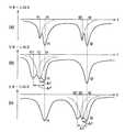
例えば、表面実装型アンテナ1が2つの異なる周波数帯域f1,f2で送受信が可能である場合に、上記周波数帯域f1,f2の両方の帯域幅を拡大したい場合を例にする。
この場合には、上記第1の無給電放射電極13と第2の無給電放射電極14のうちの一方は、図8(a)に示す放射電極3の共振周波数f1から僅かにずれた周波数f1’を共振周波数として持つように、そのミアンダピッチおよびターン数が定められる。
また、他方側は放射電極3の共振周波数f2から僅かにずれた周波数f2’を共振周波数として持つように、そのミアンダピッチおよびターン数が定められる。
【0041】
また、上記周波数帯域f1,f2のうちの一方の周波数帯域f1の帯域幅を拡大したい場合を例にする。
この場合には、上記第1の無給電放射電極13と第2の無給電放射電極14のうちの一方は、図8(b)に示す放射電極3の共振周波数f1から所定のΔfだけずれた周波数f1’を共振周波数として持つように、そのミアンダピッチおよびターン数が定められる。
また、他方側は、上記共振周波数f1から上記Δfとは異なるΔf’だけずれた周波数f1’’を共振周波数として持つように、そのミアンダピッチおよびターン数が定められる。
【0042】
さらに、上記周波数帯域f2の帯域幅を拡大したい場合を例にする。
この場合には、上記同様に、図8(c)に示すように、上記第1の無給電放射電極13と第2の無給電放射電極14のうちの一方は、放射電極3の共振周波数f2から所定のΔfだけずれた周波数f2’を共振周波数として持つように、そのミアンダピッチおよびターン数が定められる。
また、他方側は、上記共振周波数f2から上記Δfとは異なるΔf’だけずれた周波数f2’’を共振周波数として持つように、そのミアンダピッチおよびターン数が定められる。
【0043】
上記のように、第1の無給電放射電極13および第2の無給電放射電極14の各ミアンダピッチおよびターン数を定めることによって、前記周波数帯域f1,f2の所望の周波数帯域で複共振状態と成すことができることとなり、周波数帯域の帯域幅を拡大することができる。
【0044】
この第2の実施形態例では、図7に示すように、給電電極5は誘電体基体2の側面2dから底面2fに掛けて形成され、誘電体基体2の側面2bには固定電極7a,7bがそれぞれ間隔を介して形成されている。
また、誘電体基体2の側面2dには上記給電電極5に近接して導入パターン13a,14aが、さらに、固定電極7c,7dがそれぞれ形成されている。
【0045】
上記固定電極7a,7b,7c,7dと導入パターン13a,14aはそれぞれ誘電体基体2の底面2fに回り込んでいる。
【0046】
この第3の実施形態例に示す表面実装型アンテナ1は上記のように構成されており、この表面実装型アンテナ1は図9に示すように回路基板8の非グランド部8bに実装される。
このように、表面実装型アンテナ1が実装されることにより、放射電極3は給電電極5と整合回路11とを介して電力供給手段6に導通接続されることとなる。
また、固定電極7a,7b,7c,7dと導入パターン13a,14aは回路基板8の接地電極10に導通接続されてグランドに接地されることになる。
【0047】
この第3の実施形態例によれば、第1の無給電放射電極13と第2の無給電放射電極14を設けて、異なる2つの周波数帯域の少なくとも1つの周波数帯域では複共振状態にする構成とした。
この構成により、放射電極3のみの励振では所望の帯域幅が得られない周波数帯域の帯域幅を所望の幅に広げることが可能となり、広帯域化を図ることができる。
【0048】
また、この第3の実施形態例では、放射電極3のミアンダ状のパターンと、第1の無給電放射電極13および第2の無給電放射電極14の各ミアンダ状のパターンとはほぼ直交状に形成されている。
しかも、第1の無給電放射電極13の開放端と第2の無給電放射電極14の開放端は誘電体基体2の側面に形成されてグランドとの容量結合を強める構成である。
このことから、放射電極3の励振が、第1の無給電放射電極13あるいは第2の無給電放射電極14の励振に悪影響を及ぼす干渉問題をより確実に防止することができ、所望の複共振状態を得ることができる。
これにより、放射電極3と、第1の無給電放射電極13あるいは第2の無給電放射電極14間の干渉によるアンテナ特性の劣化を防止することができる。
【0049】
以下に、第4の実施形態例を説明する。
この第4の実施形態例において特徴的なことは、整合回路11を誘電体基体2の表面に形成したことである。
それ以外の構成は前記各実施形態例と同様であり、この第4の実施形態例では、上記各実施形態例と同一構成部分には同一符号を付し、その共通部分の重複説明は省略する。
【0050】
この第4の実施形態例では、図10(a)や図11(a)に示すように、誘電体基体2の表面に整合回路11が給電電極5に接続して形成されている。
【0051】
図10(b)には図10(a)に示す整合回路11の等価回路が示されている。
この図10(b)に示すように、図10(a)に示す整合回路11はコンデンサCにより整合を行うものである。
つまり、この図10(a)に示す整合回路11は、給電電極5に導通接続する導体パターン11aと、該導体パターン11aに間隙を介して対向する導体パターン11bとから成るコンデンサを有して構成されている。
【0052】
また、図11(b)には図11(a)の整合回路11の等価回路が示されている。
この図11(b)に示すように、図11(a)に示す整合回路11はインダクタLにより整合を行うものである。
つまり、図11(a)に示すように、整合回路11はミアンダ状の導体パターン11cにより構成されたインダクタを有して構成されている。
【0053】
この第4の実施形態例によれば、整合回路11を誘電体基体2に設けたので、前記各実施形態例とほぼ同様の効果を奏することができる。
その上に、整合回路11を回路基板8に設けなくともよくなり、整合回路11を設けなくともよい分、回路基板8の部品が実装される面積を縮小させることができる。
【0054】
また、整合回路11は上記のように、導体パターン11a,11bや導体パターン11cにより構成されている。
この構成により、誘電体基体2の表面に印刷技術等を用いて上記導体パターン11a,11bや11cを形成するだけで、簡単に、整合回路11を形成することができることとなり、部品点数の削減に伴い、製造コストの低減を図ることができる。
【0055】
以下に、第5の実施形態例を説明する。
この第5の実施形態例では、表面実装型アンテナを内蔵した通信機を示す。
この第5の実施形態例において特徴的なことは、上記各実施形態例に示した表面実装型アンテナ1が内蔵されていることである。
なお、この第5の実施形態例の説明において、前記各実施形態例と同一構成部分には同一符号を付し、その共通部分の重複説明は省略する。
【0056】
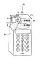
図15にはこの第5の実施形態例において特徴的な通信機である携帯型の電話機の一例が示されている。
この図15に示すように、携帯型の電話機20のケース21内には、実装基板(回路基板)8が設けられており、この実装基板8には電力供給手段6が形成されている。
上記実装基板8の接地面(接地電極)10に表面実装型アンテナ1が実装されている。
この表面実装型アンテナ1は上記各実施形態例に示した形態のうちの何れか1つの形態を備えたものである。
上記電力供給手段6は切り換え回路22を介して送信回路23と受信回路24に接続されている。
【0057】
この図5に示す通信機20においては、電力供給手段6から電力が表面実装型アンテナ1に供給されて、前述したようなアンテナ動作が行われ、切り換え回路22の切り換え動作によって、信号の送受信が円滑に行われるものである。
【0058】
この第5の実施形態例によれば、上記各実施形態例に示した表面実装型アンテナ1を内蔵したので、1つのアンテナを用いるだけで、異なる2つの周波数帯域の電波の送受信が可能になる。
このことから、通信機20の小型化を図ることができるという効果を奏することができる。
【0059】
なお、この発明は上記各実施形態例に限定されるものではなく、様々な実施の形態を採り得る。
例えば、上記各実施形態例では、誘電体基体2は直方体状であったが、誘電体基体2は、例えば、円柱状や多角柱状でもよい。
【0060】
また、上記第1〜第4の各実施形態例では、表面実装型アンテナ1は回路基板8の非グランド部8bに実装される例を示したが、本発明は、図12に示すように回路基板8の接地電極10上に実装される表面実装型アンテナ1にも適用することができるものである。
【0061】
さらに、上記各実施形態例では、放射電極3はミアンダピッチが異なる2つの電極部3a,3bが直列に接続されて成る例を示したが、放射電極3はミアンダピッチが異なる3つ以上の電極部が直列に接続されている構成としてもよい。
例えば、図13(a)に示す放射電極3はミアンダピッチd1,d2,d3の異なる3つの電極部3a,3b,3cが直列に接続されたものである。
この場合には、その放射電極3によって、表面実装型アンテナ1は、例えば、図13(b)に示すように、異なる3つの周波数帯域f1,f2,f3で放射電極3のリターンロスが低くなり、電波の送受信が可能となる。
【0062】
さらに、図14(a)、(b)、(c)に示すように、誘電体基体2に穴部17や凹部18を設けてもよい。
このように、誘電体基体2に穴部17や凹部18を設けることによって、誘電体基体2の軽量化を図ることができるという効果や、次に示すような効果を奏することが可能となる。
つまり、グランドと放射電極間の誘電率が下がり、電界集中が緩和されて、広帯域化、高利得化を実現できる。
【0063】
さらに、上記各実施形態例では、放射電極3は2つ以上の面に渡って形成されている例を示したが、第1電極部3aや第2電極部3bのミアンダピッチやターン数等に応じて放射電極3は1つの面のみに形成してもよい。
【0064】
さらに、上記第5の実施形態例では、携帯型の電話機に表面実装型アンテナ1を内蔵する例を示したが、本発明の表面実装型アンテナは携帯型の電話機以外の通信機にも内蔵することができるものであり、上記したような通信機の小型化を図ることが可能になるという効果を奏することができる。
【0065】
【発明の効果】
この発明によれば、ミアンダピッチが異なる2つ以上のミアンダ状の電極部が直列に接続されてミアンダ状の放射電極を形成したので、放射電極は、上記複数のミアンダ状の電極部に基づいた複数の共振周波数を有することとなる。
このことによって、表面実装型アンテナは少なくとも2つ以上の周波数帯域の電波の送受信が可能となる。
【0066】
放射電極が直方体状の誘電体基体の2面以上に形成されているものや、無給電放射電極が誘電体基体の2面以上に形成されているものにあっては、放射電極や無給電放射電極を誘電体基体の1面のみに形成する場合に比べて、放射電極や無給電放射電極の形成領域が広がる。
このために、放射電極や無給電放射電極の大きさに大きく規制されることなく、誘電体基体の小型化を図ることができる。
【0067】
誘電体基体の表面に無給電放射電極が形成され、表面実装型アンテナの複数の周波数帯域のうちの少なくとも1つの周波数帯域では複共振状態とするものにあっては、放射電極の励振のみでは帯域幅が狭くて所望の帯域幅の周波数帯域が得られない場合に、上記無給電放射電極によって、その狭い帯域幅の周波数帯域では複共振状態にすることで、周波数帯域の帯域幅を所望の帯域幅に拡大することができて広帯域化を図ることが可能となる。
また、表面実装型アンテナの複数の周波数帯域のうちの少なくとも1つの周波数帯域において複共振状態を作り出す手段が設けられているものにあっては、上記同様に、複共振状態とすることで広帯域化を図ることができる。
【0068】
無給電放射電極がミアンダ状に形成され、この無給電放射電極のミアンダ状のパターンと放射電極のミアンダ状のパターンとがほぼ直交状に形成されているものにあっては、放射電極の励振が無給電放射電極の励振に悪影響を及ぼす干渉問題を回避することができる。
特に、無給電放射電極の開放端がグランドと容量結合により間接的に接続されているものにあっては、その開放端とグランドとの容量結合によって、より確実に上記干渉問題を防止することができる。
このように、干渉問題を防止することができるので、放射電極の励振と無給電放射電極の励振とをそれぞれ独立的に行わせることができる。
このことにより、放射電極の励振と無給電放射電極の励振とによって、所定の周波数帯域で複共振状態にすることができる。
これにより、放射電極と無給電放射電極間の干渉によるアンテナ特性の劣化を防止することができる。
【0069】
誘電体基体の表面に整合回路を形成したものにあっては、表面実装型アンテナが実装する回路基板に上記整合回路を形成しなくて済むので、回路基板の部品が実装される面積の縮小化および部品の削減により、部品コストと実装コストの両面からコストダウンを図ることができる。
【0070】
本発明の表面実装型アンテナを用いた通信機は、1つのアンテナを用いるのみで複数の周波数帯域をカバーできるため、通信機そのものの小型化を図ることができる。
【図面の簡単な説明】
【図1】 第1の実施形態例に示す表面実装型アンテナを示す説明図である。
【図2】 第1の実施形態例の表面実装型アンテナにおける送受信可能な周波数帯域例を示す説明図である。
【図3】 第1の実施形態例における表面実装型アンテナの回路基板への実装例を示す説明図である。
【図4】 第2の実施形態例を示す説明図である。
【図5】 第2の実施形態例の実装型アンテナにおける送受信可能な周波数帯域例を示す説明図である。
【図6】 第2の実施形態例における表面実装型アンテナの回路基板への実装例を示す説明図である。
【図7】 第3の実施形態例の表面実装型アンテナを示す説明図である。
【図8】 第3の実施形態例の表面実装型アンテナにおける送受信可能な周波数帯域例を示す説明図である。
【図9】 第3の実施形態例における表面実装型アンテナの回路基板への実装例を示す説明図である。
【図10】 第4の実施形態例において特徴的な、コンデンサにより整合を行う整合回路の一例を示す説明図である。
【図11】 第4の実施形態例において特徴的な、インダクタにより整合を行う整合回路の一例を示す説明図である。
【図12】 表面実装型アンテナを回路基板の接地電極上に実装した場合の一例を示す説明図である。
【図13】 その他の実施形態例を示す説明図である。
【図14】 さらに、その他の実施形態例を示す説明図である。
【図15】 表面実装型アンテナを内蔵した通信機の一例を示す説明図である。
【図16】 表面実装型アンテナの従来例を示す説明図である。
【符号の説明】
1 表面実装型アンテナ
2 誘電体基体
2a 前端面
2c 後端面
2e 上面
3 放射電極
3a 第1電極部
3b 第2電極部
5 給電電極
6 電力供給手段
8 回路基板
11 整合回路
12 無給電放射電極
13 第1無給電放射電極
14 第2無給電放射電極
20 通信機[0001]
BACKGROUND OF THE INVENTION
The present invention relates to a surface mount antenna built in a communication device such as a portable telephone and a communication device using the same.
[0002]
[Prior art]
FIG. 16 schematically shows an example of a surface-mounted antenna incorporated in a communication device such as a mobile phone.
The
That is, the
The
[0003]
An external power supply means (power supply source) 6 is electrically connected to the
The
[0004]
[Problems to be solved by the invention]
By the way, at present, there are cases where two frequency bands of 900 MHz band and 1.9 GHz band are used as frequency bands used for portable telephones.
[0005]
However, a communication device that can use two different frequency bands requires a surface-mounted antenna that can transmit and receive radio waves in two different frequency bands with one antenna. As described above, the
[0006]
The present invention has been made to solve the above-described problems, and an object of the present invention is to provide a surface-mounted antenna capable of transmitting and receiving radio waves in two or more different frequency bands and a communication device using the same. It is in.
[0007]
[Means for Solving the Problems]
In order to achieve the above object, the present invention has the following configuration as means for solving the above problems.
That is, a surface-mounted antenna according to a first aspect of the present invention is a surface-mounted antenna that transmits and receives radio waves in at least two different frequency bands by means of radiation electrodes formed on the surface of a rectangular parallelepiped dielectric substrate. The electrode has at least a meander-shaped first electrode portion formed at a first meander pitch, and a meander-shaped second electrode portion formed at a second meander pitch narrower than the first meander pitch,the above The radiation electrode includes the first electrode portion andthe above The second electrode part is formed with a meandering radiation electrode connected in series,the above The radiation electrode includes the first electrode portion andthe above A configuration in which radio waves are transmitted and received in a frequency band in which the second electrode unit resonates together and in a frequency band in which the second electrode unit having a frequency higher than the frequency band resonates independently,The radiation electrode Of the
Therefore, it is a means for solving the problems.
[0008]
A surface mount antenna according to a second aspect of the present invention comprises the configuration of the first aspect of the present invention,the above The parasitic radiation electrode is configured to be a meandering parasitic radiation electrode.
[0009]
A surface mount antenna according to a third aspect of the present invention has the configuration of the first or second aspect of the present invention,the above The parasitic radiation electrodethe above Of dielectric substratesurface It is characterized by being formed over two or more surfaces.
[0010]
A surface-mounted antenna according to a fourth aspect of the present invention comprises the configuration of the second or third aspect of the present invention,the above The parasitic radiation electrodethe above It is formed in a part different from the radiation electrode on at least the upper surface of the dielectric substrate,The radiation electrode and the parasitic radiation electrode are provided on one of the surfaces of the dielectric substrate. It is characterized by being formed in a substantially orthogonal shape.
[0011]
A surface-mounted antenna according to a fifth invention comprises any one of the first to fourth inventions,the above The radiation electrode is configured to be conductively connected to a power supply source via a matching circuit.the above It is characterized by being provided on the surface of the dielectric substrate.
[0012]
According to a sixth aspect of the present invention, there is provided a communication device using a surface-mounted antenna, wherein the surface-mounted antenna constituting any one of the first to fifth inventions is mounted on a mounting substrate. It is configured.
[0013]
In the invention having the above-described configuration, the radiation electrode formed on the surface of the dielectric substrate is a meander-shaped radiation electrode in which at least a meander-shaped first electrode portion and a meander-shaped second electrode portion are connected in series. . Here, the resonance frequency of the meander electrode portion is determined by the meander pitch and the number of turns (electric length). Therefore, as in the present invention, by connecting a plurality of electrode portions having different meander pitches in series to form a radiation electrode, the radiation electrode has a plurality of resonance frequencies. For this reason, the surface-mounted antenna of the present invention can transmit and receive radio waves in a plurality of different frequency bands. In addition, since the communication device of the present invention can cover a plurality of frequency bands with one antenna, it can be miniaturized.
[0014]
DETAILED DESCRIPTION OF THE INVENTION
Embodiments according to the present invention will be described below with reference to the drawings.
[0015]
FIG. 1A shows a schematic perspective view of a surface mount antenna according to the first embodiment, and FIG. 1B shows the surface mount antenna according to the first embodiment. The surface form of the dielectric substrate is shown in a developed state.
[0016]
As shown in FIGS. 1A and 1B, the surface-mounted
[0017]
The
The meander pitch (hereinafter referred to as the first meander pitch) d1 of the
[0018]
The first meander pitch d1 and the number of turns of the
For example, as shown in FIG. 2, two different frequencies of a first frequency band f1 (for example, 900 MHz band) and a second frequency band f2 (for example, 1.9 GHz band) higher than the first frequency band f1. The case where the return loss is reduced in the band, that is, the case where the surface-mounted
In this case, the
[0019]
The ratio between the first meander pitch d1 and the second meander pitch d2 and the interval H between the frequencies f1 and f2 shown in FIG.
Therefore, the first meander pitch d1 of the
Further, the number of turns of the
In the example of FIG. 1, the
[0020]
As shown in FIG. 1B, a feeding
Further, a fixed
[0021]
Further, fixed
The feeding
[0022]
The
In other words, the
In the example shown in FIG. 3, the
[0023]
The
The surface-mounted
Power is supplied from the power supply means 6 to the
Further, when only the
[0024]
According to the first embodiment, the
As a result, the surface-mounted
[0025]
In the first embodiment, the
Therefore, the area where the
For this reason, the
In the first embodiment, the
As described above, when the
[0026]
The second embodiment will be described below.
In the description of the second embodiment, the same components as those in the first embodiment are denoted by the same reference numerals, and duplicate descriptions of common portions are omitted.
[0027]
As described in the first embodiment, the radiating
However, one of the frequency bands f1 and f2 may be narrower than a desired width.
[0028]
Therefore, in the second embodiment, the following configuration is provided in order to expand the bandwidth of the frequency band having a narrower bandwidth than the desired bandwidth.
FIG. 4 shows the surface form of the dielectric substrate constituting the surface mount antenna according to the second embodiment in a developed state.
The second embodiment is characterized in that a
The
An
[0029]
The meander pitch and the number of turns of the
For example, when it is desired to expand the bandwidth of the frequency band f1 of the frequency bands f1 and f2 (in other words, to increase the bandwidth), the resonance frequency f1 of the
When the
On the other hand, the
For this reason, the
[0030]
When it is desired to expand the bandwidth of the frequency band f2, the parasitic radiation electrode has a frequency f2 ′ slightly shifted from the resonance frequency f2 of the
When the
[0031]
As shown in FIG. 4, in the second embodiment, the feeding
As in the first embodiment, the
The meandering
In other words, the meandering pattern of the
One end side of the
[0032]
Further, as shown in FIG. 4, fixed
These fixed
[0033]
The
For example, as shown in FIG. 6, the surface-mounted
As described above, when the surface-mounted
The fixed
[0034]
When power is supplied from the power supply means 6 to the
When the
In addition, when the
[0035]
According to the second embodiment, the
For this reason, it is possible to widen the bandwidth of a desired frequency band out of the frequency bands f1 and f2, and a wider band can be achieved.
[0036]
In the second embodiment, the meandering pattern of the
For this reason, it is possible to avoid an interference problem in which the excitation of the
Thereby, deterioration of the antenna characteristics due to interference between the
[0037]
The third embodiment will be described below.
In the description of the third embodiment, the same reference numerals are given to the same components as those in each of the above embodiments, and the overlapping description of the common portions is omitted.
[0038]
FIG. 7 shows the surface form of the dielectric substrate constituting the surface mount antenna of the third embodiment according to the developed state.
What is characteristic in the third embodiment is that a first
[0039]
In the third embodiment, as shown in FIG. 7, the meandering
The first
That is, the first
The second
Thus, each meandering pattern of the first
[0040]
The meander pitch and the number of turns of the first
For example, when the surface-mounted
In this case, one of the first
Further, the meander pitch and the number of turns are determined so that the other side has a frequency f2 ′ slightly shifted from the resonance frequency f2 of the
[0041]
Further, a case where it is desired to increase the bandwidth of one of the frequency bands f1 and f2 is taken as an example.
In this case, one of the first
On the other side, the meander pitch and the number of turns are determined so that the resonance frequency has a frequency f1 ″ shifted from the resonance frequency f1 by Δf ′ different from Δf.
[0042]
Furthermore, the case where it is desired to expand the bandwidth of the frequency band f2 is taken as an example.
In this case, similarly to the above, as shown in FIG. 8C, one of the first
On the other side, the meander pitch and the number of turns are determined so that the resonance frequency has a frequency f2 ″ shifted from the resonance frequency f2 by Δf ′ different from Δf.
[0043]
As described above, by determining the meander pitch and the number of turns of the first
[0044]
In the second embodiment, as shown in FIG. 7, the feeding
In addition,
[0045]
The fixed
[0046]
The surface-mounted
As described above, by mounting the
The fixed
[0047]
According to the third embodiment, the first
With this configuration, it becomes possible to widen the bandwidth of a frequency band where a desired bandwidth cannot be obtained by excitation with only the
[0048]
In the third embodiment, the meandering pattern of the
Moreover, the open end of the first
Therefore, it is possible to more reliably prevent the interference problem that the excitation of the
Thereby, it is possible to prevent deterioration of antenna characteristics due to interference between the
[0049]
The fourth embodiment will be described below.
What is characteristic in the fourth embodiment is that the matching
The rest of the configuration is the same as in each of the above-described embodiments. In this fourth embodiment, the same components as those in the above-described embodiments are denoted by the same reference numerals, and redundant description of common portions is omitted. .
[0050]
In the fourth embodiment, as shown in FIG. 10A and FIG. 11A, a matching
[0051]
FIG. 10B shows an equivalent circuit of the matching
As shown in FIG. 10B, the matching
That is, the matching
[0052]
FIG. 11B shows an equivalent circuit of the matching
As shown in FIG. 11B, the matching
That is, as shown in FIG. 11A, the matching
[0053]
According to the fourth embodiment, since the matching
In addition, it is not necessary to provide the
[0054]
Further, the matching
With this configuration, the matching
[0055]
The fifth embodiment will be described below.
In the fifth embodiment, a communication device incorporating a surface mount antenna is shown.
What is characteristic in the fifth embodiment is that the
In the description of the fifth embodiment, the same reference numerals are given to the same components as those in each of the above embodiments, and the overlapping description of the common portions will be omitted.
[0056]
FIG. 15 shows an example of a portable telephone which is a characteristic communication device in the fifth embodiment.
As shown in FIG. 15, a mounting board (circuit board) 8 is provided in a
The
The
The power supply means 6 is connected to a
[0057]
In the
[0058]
According to the fifth embodiment, since the
From this, it is possible to achieve an effect that the
[0059]
The present invention is not limited to the above embodiments, and various embodiments can be adopted.
For example, in each of the above embodiments, the
[0060]
In the first to fourth embodiments, the surface-mounted
[0061]
Further, in each of the above embodiments, the
For example, the
In this case, due to the
[0062]
Furthermore, as shown in FIGS. 14A, 14 </ b> B, and 14 </ b> C, a
As described above, by providing the
That is, the dielectric constant between the ground and the radiation electrode is lowered, the electric field concentration is relaxed, and a wide band and a high gain can be realized.
[0063]
Further, in each of the above embodiments, the
[0064]
Further, in the fifth embodiment, the example in which the surface-mounted
[0065]
【The invention's effect】
According to this invention, since two or more meander-shaped electrode portions having different meander pitches are connected in series to form a meander-shaped radiation electrode, the radiation electrode is based on the plurality of meander-shaped electrode portions. It has a plurality of resonance frequencies.
As a result, the surface-mounted antenna can transmit and receive radio waves in at least two frequency bands.
[0066]
When the radiation electrode is formed on two or more surfaces of a rectangular parallelepiped dielectric substrate or when the parasitic radiation electrode is formed on two or more surfaces of the dielectric substrate, the radiation electrode or parasitic radiation is used. Compared with the case where the electrode is formed on only one surface of the dielectric substrate, the area where the radiation electrode and the parasitic radiation electrode are formed is expanded.
For this reason, the dielectric substrate can be downsized without being largely restricted by the size of the radiation electrode or the parasitic radiation electrode.
[0067]
In the case where a parasitic radiation electrode is formed on the surface of the dielectric substrate and a multi-resonant state is obtained in at least one frequency band of a plurality of frequency bands of the surface mount antenna, the band is obtained only by excitation of the radiation electrode. When the frequency band of a desired bandwidth cannot be obtained due to the narrow width, the parasitic radiation electrode makes the frequency band of the desired band by making a double resonance state in the narrow bandwidth of the frequency band. It is possible to increase the width and widen the bandwidth.
In addition, in the case where a means for creating a multiple resonance state in at least one frequency band of a plurality of frequency bands of the surface mount antenna is provided, as in the above case, it is possible to increase the bandwidth by setting the multiple resonance state. Can be achieved.
[0068]
When the parasitic radiation electrode is formed in a meander shape and the meandering pattern of the parasitic radiation electrode and the meandering pattern of the radiation electrode are formed substantially orthogonal, the excitation of the radiation electrode is Interference problems that adversely affect excitation of the parasitic radiation electrode can be avoided.
In particular, in the case where the open end of the parasitic radiation electrode is indirectly connected to the ground by capacitive coupling, the interference problem can be more reliably prevented by capacitive coupling between the open end and the ground. it can.
Thus, since the interference problem can be prevented, the excitation of the radiation electrode and the excitation of the parasitic radiation electrode can be performed independently.
Thus, a double resonance state can be achieved in a predetermined frequency band by excitation of the radiation electrode and excitation of the parasitic radiation electrode.
Thereby, it is possible to prevent deterioration of the antenna characteristics due to interference between the radiation electrode and the parasitic radiation electrode.
[0069]
In the case where a matching circuit is formed on the surface of a dielectric substrate, it is not necessary to form the matching circuit on the circuit board on which the surface mount antenna is mounted. In addition, by reducing the number of parts, it is possible to reduce costs in terms of both part cost and mounting cost.
[0070]
Since the communication device using the surface mount antenna of the present invention can cover a plurality of frequency bands by using only one antenna, the communication device itself can be downsized.
[Brief description of the drawings]
FIG. 1 is an explanatory diagram showing a surface mount antenna shown in a first embodiment.
FIG. 2 is an explanatory diagram showing an example of a frequency band that can be transmitted and received in the surface-mounted antenna according to the first embodiment.
FIG. 3 is an explanatory diagram showing an example of mounting the surface-mounted antenna on the circuit board in the first embodiment.
FIG. 4 is an explanatory diagram showing a second embodiment.
FIG. 5 is an explanatory diagram showing an example of frequency bands that can be transmitted and received in the mounting antenna according to the second embodiment.
FIG. 6 is an explanatory diagram showing an example of mounting a surface-mounted antenna on a circuit board in the second embodiment.
FIG. 7 is an explanatory diagram showing a surface-mounted antenna according to a third embodiment.
FIG. 8 is an explanatory diagram showing an example of frequency bands that can be transmitted and received in the surface-mounted antenna according to the third embodiment.
FIG. 9 is an explanatory diagram showing an example of mounting a surface-mounted antenna on a circuit board in a third embodiment.
FIG. 10 is an explanatory diagram showing an example of a matching circuit that performs matching using a capacitor, which is characteristic in the fourth embodiment.
FIG. 11 is an explanatory diagram showing an example of a matching circuit that performs matching using an inductor, which is characteristic in the fourth embodiment.
FIG. 12 is an explanatory diagram showing an example when a surface-mounted antenna is mounted on a ground electrode of a circuit board.
FIG. 13 is an explanatory diagram showing another embodiment.
FIG. 14 is an explanatory diagram showing another embodiment.
FIG. 15 is an explanatory diagram showing an example of a communication device incorporating a surface-mounted antenna.
FIG. 16 is an explanatory view showing a conventional example of a surface mount antenna.
[Explanation of symbols]
1 Surface mount antenna
2 Dielectric substrate
2a Front end face
2c Rear end face
2e Top surface
3 Radiation electrode
3a 1st electrode part
3b Second electrode part
5 Feeding electrode
6 Power supply means
8 Circuit board
11 Matching circuit
12 Parasitic radiation electrode
13 First parasitic radiation electrode
14 Second parasitic radiation electrode
20 communication equipment
Claims (6)
Translated fromJapanesePriority Applications (5)
| Application Number | Priority Date | Filing Date | Title |
|---|---|---|---|
| JP2000111820AJP3639767B2 (en) | 1999-06-24 | 2000-04-13 | Surface mount antenna and communication device using the same |
| CA002310682ACA2310682C (en) | 1999-06-24 | 2000-06-02 | Surface-mount antenna and communication apparatus using the same |
| US09/593,072US6320545B1 (en) | 1999-06-24 | 2000-06-13 | Surface-mount antenna and communication apparatus using the same |
| DE10030402ADE10030402B4 (en) | 1999-06-24 | 2000-06-21 | Surface mounting antenna and communication device using the same |
| CNB001192566ACN1159803C (en) | 1999-06-24 | 2000-06-23 | Surface mount antenna and communication equipment using it |
Applications Claiming Priority (3)
| Application Number | Priority Date | Filing Date | Title |
|---|---|---|---|
| JP11-177961 | 1999-06-24 | ||
| JP17796199 | 1999-06-24 | ||
| JP2000111820AJP3639767B2 (en) | 1999-06-24 | 2000-04-13 | Surface mount antenna and communication device using the same |
Publications (2)
| Publication Number | Publication Date |
|---|---|
| JP2001068917A JP2001068917A (en) | 2001-03-16 |
| JP3639767B2true JP3639767B2 (en) | 2005-04-20 |
Family
ID=26498309
Family Applications (1)
| Application Number | Title | Priority Date | Filing Date |
|---|---|---|---|
| JP2000111820AExpired - Fee RelatedJP3639767B2 (en) | 1999-06-24 | 2000-04-13 | Surface mount antenna and communication device using the same |
Country Status (5)
| Country | Link |
|---|---|
| US (1) | US6320545B1 (en) |
| JP (1) | JP3639767B2 (en) |
| CN (1) | CN1159803C (en) |
| CA (1) | CA2310682C (en) |
| DE (1) | DE10030402B4 (en) |
Families Citing this family (79)
| Publication number | Priority date | Publication date | Assignee | Title |
|---|---|---|---|---|
| US7190319B2 (en)* | 2001-10-29 | 2007-03-13 | Forster Ian J | Wave antenna wireless communication device and method |
| JP3658639B2 (en)* | 2000-04-11 | 2005-06-08 | 株式会社村田製作所 | Surface mount type antenna and radio equipped with the antenna |
| JP3640595B2 (en)* | 2000-05-18 | 2005-04-20 | シャープ株式会社 | Multilayer pattern antenna and wireless communication apparatus including the same |
| US6630906B2 (en)* | 2000-07-24 | 2003-10-07 | The Furukawa Electric Co., Ltd. | Chip antenna and manufacturing method of the same |
| FR2812766B1 (en)* | 2000-08-01 | 2006-10-06 | Sagem | ANTENNA WITH SURFACE (S) RADIANT (S) PLANE (S) AND PORTABLE TELEPHONE COMPRISING SUCH ANTENNA |
| US6597320B2 (en)* | 2000-09-11 | 2003-07-22 | Nippon Soken, Inc. | Antenna for portable radio communication device and method of transmitting radio signal |
| JP4522564B2 (en)* | 2000-09-22 | 2010-08-11 | 富士通株式会社 | Electronics |
| KR100374174B1 (en)* | 2000-10-24 | 2003-03-03 | 주식회사 에이스테크놀로지 | A wideband internal antenna |
| DE60120894T2 (en) | 2000-12-26 | 2007-01-11 | The Furukawa Electric Co., Ltd. | Manufacturing method of an antenna |
| US7038635B2 (en)* | 2000-12-28 | 2006-05-02 | Matsushita Electric Industrial Co., Ltd. | Antenna, and communication device using the same |
| CN2476881Y (en)* | 2000-12-30 | 2002-02-13 | 深圳市中兴通讯股份有限公司 | Built-in planar aerial for mobile phone |
| TW513827B (en) | 2001-02-07 | 2002-12-11 | Furukawa Electric Co Ltd | Antenna apparatus |
| US6466174B2 (en)* | 2001-02-08 | 2002-10-15 | Centurion Wireless Technologies, Inc. | Surface mount CHIP antenna |
| US6639559B2 (en)* | 2001-03-07 | 2003-10-28 | Hitachi Ltd. | Antenna element |
| JP2002299933A (en)* | 2001-04-02 | 2002-10-11 | Murata Mfg Co Ltd | Electrode structure for antenna and communication equipment provided with the same |
| JP3678167B2 (en) | 2001-05-02 | 2005-08-03 | 株式会社村田製作所 | ANTENNA DEVICE AND RADIO COMMUNICATION DEVICE HAVING THE ANTENNA DEVICE |
| JP2002359514A (en)* | 2001-05-31 | 2002-12-13 | Anten Corp | Helical antenna |
| JP2003069330A (en)* | 2001-06-15 | 2003-03-07 | Hitachi Metals Ltd | Surface-mounted antenna and communication apparatus mounting the same |
| KR100413010B1 (en)* | 2001-07-02 | 2003-12-31 | (주) 래트론 | A small dielectric antenna |
| KR100423396B1 (en)* | 2001-07-02 | 2004-03-18 | 삼성전기주식회사 | A Chip Antenna |
| DE60212429T2 (en) | 2001-10-11 | 2007-09-20 | Taiyo Yuden Co., Ltd. | DIELECTRIC ANTENNA |
| WO2003038747A2 (en) | 2001-10-29 | 2003-05-08 | Marconi Intellectual Property (Us) Inc | Wave antenna wireless communication device |
| US6630910B2 (en) | 2001-10-29 | 2003-10-07 | Marconi Communications Inc. | Wave antenna wireless communication device and method |
| WO2003046824A2 (en)* | 2001-11-21 | 2003-06-05 | Marconi Intellectual Property (Us) Inc. | Wireless communication device interconnectivity |
| EP1688871B1 (en)* | 2001-11-21 | 2008-08-27 | Mineral Lassen LLC | Wireless communication device interconnectivity |
| KR100455120B1 (en)* | 2002-02-01 | 2004-11-06 | 엘지전자 주식회사 | Meander slot antenna and manufacturing method thereof |
| US6639564B2 (en) | 2002-02-13 | 2003-10-28 | Gregory F. Johnson | Device and method of use for reducing hearing aid RF interference |
| KR100477271B1 (en)* | 2002-05-15 | 2005-03-22 | (주) 코산아이엔티 | Micro chip dual band antenna |
| KR100532223B1 (en)* | 2002-05-15 | 2005-11-29 | (주) 코산아이엔티 | Micro chip dual band antenna |
| DE10258184A1 (en)* | 2002-12-12 | 2004-07-15 | Siemens Ag | Antenna structure for two overlapping frequency bands |
| EP1441414A1 (en)* | 2003-01-23 | 2004-07-28 | Alps Electric Co., Ltd. | Dual band antenna with reduced size and height |
| JP2004228984A (en) | 2003-01-23 | 2004-08-12 | Alps Electric Co Ltd | Antenna assembly |
| US6914567B2 (en)* | 2003-02-14 | 2005-07-05 | Centurion Wireless Technologies, Inc. | Broadband combination meanderline and patch antenna |
| CN1324761C (en)* | 2003-03-03 | 2007-07-04 | 正文科技股份有限公司 | dual frequency antenna |
| US7501984B2 (en) | 2003-11-04 | 2009-03-10 | Avery Dennison Corporation | RFID tag using a surface insensitive antenna structure |
| US7652636B2 (en) | 2003-04-10 | 2010-01-26 | Avery Dennison Corporation | RFID devices having self-compensating antennas and conductive shields |
| US6914562B2 (en)* | 2003-04-10 | 2005-07-05 | Avery Dennison Corporation | RFID tag using a surface insensitive antenna structure |
| CN1778014B (en)* | 2003-06-04 | 2011-06-15 | 株式会社村田制作所 | Frequency-variable antenna and communication device having the same |
| KR20030064717A (en)* | 2003-07-15 | 2003-08-02 | 학교법인 한국정보통신학원 | An internal triple-band antenna |
| GB0318134D0 (en)* | 2003-08-01 | 2003-09-03 | Gatan Uk | Specimen tip and tip holder assembly |
| US7148851B2 (en)* | 2003-08-08 | 2006-12-12 | Hitachi Metals, Ltd. | Antenna device and communications apparatus comprising same |
| JP4263972B2 (en)* | 2003-09-11 | 2009-05-13 | 京セラ株式会社 | Surface mount antenna, antenna device, and wireless communication device |
| EP1719207A2 (en)* | 2004-02-18 | 2006-11-08 | Koninklijke Philips Electronics N.V. | Antenna |
| KR100674667B1 (en) | 2004-05-14 | 2007-01-25 | 경기대학교 | Dual band small chip antenna with stacked meander structure for wireless mobile terminal |
| CN100379085C (en)* | 2004-06-22 | 2008-04-02 | 明基电通股份有限公司 | Antenna device and mobile unit using the same |
| JP2006080721A (en)* | 2004-09-08 | 2006-03-23 | Nec Corp | Antenna device and portable radio device |
| US7501955B2 (en)* | 2004-09-13 | 2009-03-10 | Avery Dennison Corporation | RFID device with content insensitivity and position insensitivity |
| TWI246226B (en)* | 2004-10-14 | 2005-12-21 | Mediatek Inc | Dual band antenna device, wireless communication device and radio frequency chip using the same |
| JP4663346B2 (en)* | 2005-02-01 | 2011-04-06 | 富士通株式会社 | Meander line antenna |
| US7274334B2 (en)* | 2005-03-24 | 2007-09-25 | Tdk Corporation | Stacked multi-resonator antenna |
| TW200707842A (en)* | 2005-08-08 | 2007-02-16 | Wistron Neweb Corp | Antenna structure |
| US7528791B2 (en)* | 2005-08-08 | 2009-05-05 | Wistron Neweb Corporation | Antenna structure having a feed element formed on an opposite surface of a substrate from a ground portion and a radiating element |
| US7265726B2 (en)* | 2005-09-26 | 2007-09-04 | Motorola, Inc. | Multi-band antenna |
| JP2007123982A (en)* | 2005-10-25 | 2007-05-17 | Sony Ericsson Mobilecommunications Japan Inc | Multiband compatible antenna system and communication terminal |
| US20070164909A1 (en)* | 2006-01-13 | 2007-07-19 | Ogawa Harry K | Embedded antenna of a mobile device |
| GB0609871D0 (en) | 2006-05-17 | 2006-06-28 | Transense Technologies Plc | Runflat safety band incorporating wireless device |
| US8432313B2 (en)* | 2006-06-23 | 2013-04-30 | Nokia Corporation | Conformal and compact wideband antenna |
| US20080024366A1 (en)* | 2006-07-25 | 2008-01-31 | Arcadyan Technology Corporation | Dual band flat antenna |
| JP4586998B2 (en)* | 2007-03-23 | 2010-11-24 | 日立金属株式会社 | Chip antenna, antenna device using the same, and wireless communication device |
| JP4661816B2 (en)* | 2007-03-30 | 2011-03-30 | 株式会社村田製作所 | Antenna and wireless communication device |
| KR100899293B1 (en)* | 2007-04-04 | 2009-05-27 | 주식회사 이엠따블유안테나 | Broadband Antenna by Double Resonance |
| US7705783B2 (en)* | 2007-04-06 | 2010-04-27 | Research In Motion Limited | Slot-strip antenna apparatus for a radio device operable over multiple frequency bands |
| US8972021B2 (en) | 2008-03-04 | 2015-03-03 | Cardiac Pacemakers, Inc. | Detachable helical antenna for implantable medical device |
| US8588924B2 (en) | 2008-03-04 | 2013-11-19 | Cardiac Pacemakers, Inc. | Loaded RF antenna for implantable device |
| AU2009220198B2 (en) | 2008-03-04 | 2012-11-29 | Cardiac Pacemakers, Inc. | Implantable multi-length RF antenna |
| US8305286B2 (en)* | 2009-05-29 | 2012-11-06 | Cisco Technology, Inc. | Mounting an antenna system to a solid surface |
| WO2011087123A1 (en)* | 2010-01-18 | 2011-07-21 | 株式会社フジクラ | Antenna device and antenna system |
| JP2011193088A (en)* | 2010-03-12 | 2011-09-29 | Sony Corp | High-frequency coupler, and communication device |
| JP5626483B2 (en)* | 2012-06-08 | 2014-11-19 | 株式会社村田製作所 | Antenna and wireless communication device |
| KR101378847B1 (en)* | 2012-07-27 | 2014-03-27 | 엘에스엠트론 주식회사 | Internal antenna with wideband characteristic |
| US10283854B2 (en)* | 2012-10-08 | 2019-05-07 | Taoglas Group Holdings Limited | Low-cost ultra wideband LTE antenna |
| CN103022014A (en)* | 2012-11-06 | 2013-04-03 | 日月光半导体制造股份有限公司 | Packaging module structure with antenna and manufacturing method thereof |
| TWI617083B (en)* | 2013-06-20 | 2018-03-01 | 群邁通訊股份有限公司 | Antenna structure and wireless communication device using same |
| JP5676722B1 (en)* | 2013-11-13 | 2015-02-25 | 三井造船株式会社 | Planar antenna and radar device |
| JP6190409B2 (en)* | 2014-06-06 | 2017-08-30 | 原田工業株式会社 | In-vehicle antenna device |
| WO2020062293A1 (en) | 2018-09-30 | 2020-04-02 | 华为技术有限公司 | Antenna and terminal |
| TWI738343B (en)* | 2020-05-18 | 2021-09-01 | 為昇科科技股份有限公司 | Meander antenna structure |
| CN112563737B (en)* | 2020-11-02 | 2022-02-11 | 中山大学 | Dual-frequency antenna comprising periodic leaky-wave structure and manufacturing method thereof |
| TWI760197B (en)* | 2021-04-27 | 2022-04-01 | 和碩聯合科技股份有限公司 | Antenna module |
Family Cites Families (7)
| Publication number | Priority date | Publication date | Assignee | Title |
|---|---|---|---|---|
| US5363114A (en)* | 1990-01-29 | 1994-11-08 | Shoemaker Kevin O | Planar serpentine antennas |
| JPH05347507A (en)* | 1992-06-12 | 1993-12-27 | Junkosha Co Ltd | Antenna |
| JP3319268B2 (en)* | 1996-02-13 | 2002-08-26 | 株式会社村田製作所 | Surface mount antenna and communication device using the same |
| JP3296189B2 (en)* | 1996-06-03 | 2002-06-24 | 三菱電機株式会社 | Antenna device |
| FI112983B (en)* | 1997-12-10 | 2004-02-13 | Nokia Corp | Antenna |
| SE9801381D0 (en)* | 1998-04-20 | 1998-04-20 | Allgon Ab | Ground extension arrangement for coupling to ground means in an antenna system, and an antenna system and a mobile radio device having such ground arrangement |
| US6124831A (en)* | 1999-07-22 | 2000-09-26 | Ericsson Inc. | Folded dual frequency band antennas for wireless communicators |
- 2000
- 2000-04-13JPJP2000111820Apatent/JP3639767B2/ennot_activeExpired - Fee Related
- 2000-06-02CACA002310682Apatent/CA2310682C/ennot_activeExpired - Fee Related
- 2000-06-13USUS09/593,072patent/US6320545B1/ennot_activeExpired - Lifetime
- 2000-06-21DEDE10030402Apatent/DE10030402B4/ennot_activeExpired - Fee Related
- 2000-06-23CNCNB001192566Apatent/CN1159803C/ennot_activeExpired - Fee Related
Also Published As
| Publication number | Publication date |
|---|---|
| CA2310682A1 (en) | 2000-12-24 |
| JP2001068917A (en) | 2001-03-16 |
| CN1279521A (en) | 2001-01-10 |
| CN1159803C (en) | 2004-07-28 |
| US6320545B1 (en) | 2001-11-20 |
| DE10030402A1 (en) | 2001-02-08 |
| DE10030402B4 (en) | 2008-05-15 |
| CA2310682C (en) | 2003-05-06 |
Similar Documents
| Publication | Publication Date | Title |
|---|---|---|
| JP3639767B2 (en) | Surface mount antenna and communication device using the same | |
| KR100663018B1 (en) | Antenna and radio communication apparatus | |
| US7466277B2 (en) | Antenna device and wireless communication apparatus | |
| EP1569300B1 (en) | Wireless device having antenna | |
| JP3562512B2 (en) | Surface mounted antenna and communication device provided with the antenna | |
| JP3658639B2 (en) | Surface mount type antenna and radio equipped with the antenna | |
| JP3843429B2 (en) | Electronic equipment and printed circuit board mounted with antenna | |
| US6456249B1 (en) | Single or dual band parasitic antenna assembly | |
| EP1289052B1 (en) | Antenna with an integral RF circuit, antenna module and communication apparatus incorporating the same | |
| US20070040749A1 (en) | Surface mount antenna apparatus having triple land structure | |
| JP2002319811A (en) | Plural resonance antenna | |
| JP2004007559A (en) | Multi-resonance antenna, antenna module, and wireless device using multi-resonance antenna | |
| JPH09219619A (en) | Surface mount antenna and communication equipment using the same | |
| JP2004088218A (en) | Planar antenna | |
| KR20050054478A (en) | Dielectric antenna and communication device incorporating the same | |
| US20070057849A1 (en) | Antenna for dual band operation | |
| US6982673B2 (en) | Inverted-F metal plate antenna having increased bandwidth | |
| KR20100079243A (en) | Infinite wavelength antenna apparatus | |
| JP2008177888A (en) | Multi-frequency antenna | |
| US6697023B1 (en) | Built-in multi-band mobile phone antenna with meandering conductive portions | |
| KR20080016353A (en) | Multiband antenna | |
| JP3042386B2 (en) | Surface mount antenna and communication device using the same | |
| JP4228559B2 (en) | Surface mount antenna and communication device using the same | |
| JP3554972B2 (en) | Surface mount antenna, antenna mounting structure, and wireless device | |
| JPH09232854A (en) | Small planar antenna device for mobile radio |
Legal Events
| Date | Code | Title | Description |
|---|---|---|---|
| A521 | Written amendment | Free format text:JAPANESE INTERMEDIATE CODE: A523 Effective date:20041028 | |
| A61 | First payment of annual fees (during grant procedure) | Free format text:JAPANESE INTERMEDIATE CODE: A61 Effective date:20050117 | |
| R150 | Certificate of patent or registration of utility model | Free format text:JAPANESE INTERMEDIATE CODE: R150 | |
| FPAY | Renewal fee payment (event date is renewal date of database) | Free format text:PAYMENT UNTIL: 20090121 Year of fee payment:4 | |
| FPAY | Renewal fee payment (event date is renewal date of database) | Free format text:PAYMENT UNTIL: 20090121 Year of fee payment:4 | |
| FPAY | Renewal fee payment (event date is renewal date of database) | Free format text:PAYMENT UNTIL: 20100121 Year of fee payment:5 | |
| FPAY | Renewal fee payment (event date is renewal date of database) | Free format text:PAYMENT UNTIL: 20110121 Year of fee payment:6 | |
| FPAY | Renewal fee payment (event date is renewal date of database) | Free format text:PAYMENT UNTIL: 20110121 Year of fee payment:6 | |
| FPAY | Renewal fee payment (event date is renewal date of database) | Free format text:PAYMENT UNTIL: 20120121 Year of fee payment:7 | |
| FPAY | Renewal fee payment (event date is renewal date of database) | Free format text:PAYMENT UNTIL: 20120121 Year of fee payment:7 | |
| FPAY | Renewal fee payment (event date is renewal date of database) | Free format text:PAYMENT UNTIL: 20130121 Year of fee payment:8 | |
| FPAY | Renewal fee payment (event date is renewal date of database) | Free format text:PAYMENT UNTIL: 20130121 Year of fee payment:8 | |
| FPAY | Renewal fee payment (event date is renewal date of database) | Free format text:PAYMENT UNTIL: 20140121 Year of fee payment:9 | |
| LAPS | Cancellation because of no payment of annual fees |