JP3636657B2 - Clock and data recovery circuit and clock control method thereof - Google Patents
Clock and data recovery circuit and clock control method thereofDownload PDFInfo
- Publication number
- JP3636657B2 JP3636657B2JP2000389526AJP2000389526AJP3636657B2JP 3636657 B2JP3636657 B2JP 3636657B2JP 2000389526 AJP2000389526 AJP 2000389526AJP 2000389526 AJP2000389526 AJP 2000389526AJP 3636657 B2JP3636657 B2JP 3636657B2
- Authority
- JP
- Japan
- Prior art keywords
- clock
- output
- circuit
- input
- phase
- Prior art date
- Legal status (The legal status is an assumption and is not a legal conclusion. Google has not performed a legal analysis and makes no representation as to the accuracy of the status listed.)
- Expired - Fee Related
Links
- 238000011084recoveryMethods0.000titleclaimsdescription32
- 238000000034methodMethods0.000titleclaimsdescription8
- 239000003990capacitorSubstances0.000claimsdescription34
- 230000007704transitionEffects0.000claimsdescription22
- 230000010363phase shiftEffects0.000claimsdescription19
- 238000001514detection methodMethods0.000claimsdescription14
- 230000003111delayed effectEffects0.000claimsdescription4
- 238000007599dischargingMethods0.000claimsdescription3
- 238000012935AveragingMethods0.000claimsdescription2
- 230000007423decreaseEffects0.000claimsdescription2
- 230000000737periodic effectEffects0.000claims1
- 102100040101Proto-oncogene serine/threonine-protein kinase mosHuman genes0.000description69
- 238000010586diagramMethods0.000description29
- 230000000630rising effectEffects0.000description23
- 102100040862Dual specificity protein kinase CLK1Human genes0.000description4
- 101150110971CIN7 geneProteins0.000description3
- 101100286980Daucus carota INV2 geneProteins0.000description3
- 101150110298INV1 geneProteins0.000description3
- 102100024061Integrator complex subunit 1Human genes0.000description3
- 101710092857Integrator complex subunit 1Proteins0.000description3
- 102100030148Integrator complex subunit 8Human genes0.000description3
- 101710092891Integrator complex subunit 8Proteins0.000description3
- 101100397044Xenopus laevis invs-a geneProteins0.000description3
- 101100397045Xenopus laevis invs-b geneProteins0.000description3
- 238000005070samplingMethods0.000description3
- 101710169754CD-NTase-associated protein 12Proteins0.000description2
- 101000749294Homo sapiens Dual specificity protein kinase CLK1Proteins0.000description2
- 238000009499grossingMethods0.000description2
- 101710169705CD-NTase-associated protein 13Proteins0.000description1
- 101100508840Daucus carota INV3 geneProteins0.000description1
- 230000000295complement effectEffects0.000description1
- 239000013256coordination polymerSubstances0.000description1
- 239000013078crystalSubstances0.000description1
- 230000003247decreasing effectEffects0.000description1
- 230000000694effectsEffects0.000description1
- 125000005842heteroatomChemical group0.000description1
- 230000010355oscillationEffects0.000description1
- 230000001360synchronised effectEffects0.000description1
- 238000003079width controlMethods0.000description1
Images


Classifications
- H—ELECTRICITY
- H03—ELECTRONIC CIRCUITRY
- H03L—AUTOMATIC CONTROL, STARTING, SYNCHRONISATION OR STABILISATION OF GENERATORS OF ELECTRONIC OSCILLATIONS OR PULSES
- H03L7/00—Automatic control of frequency or phase; Synchronisation
- H—ELECTRICITY
- H04—ELECTRIC COMMUNICATION TECHNIQUE
- H04L—TRANSMISSION OF DIGITAL INFORMATION, e.g. TELEGRAPHIC COMMUNICATION
- H04L7/00—Arrangements for synchronising receiver with transmitter
- H04L7/02—Speed or phase control by the received code signals, the signals containing no special synchronisation information
- H04L7/033—Speed or phase control by the received code signals, the signals containing no special synchronisation information using the transitions of the received signal to control the phase of the synchronising-signal-generating means, e.g. using a phase-locked loop
- H04L7/0337—Selecting between two or more discretely delayed clocks or selecting between two or more discretely delayed received code signals
- H—ELECTRICITY
- H03—ELECTRONIC CIRCUITRY
- H03K—PULSE TECHNIQUE
- H03K5/00—Manipulating of pulses not covered by one of the other main groups of this subclass
- H03K5/13—Arrangements having a single output and transforming input signals into pulses delivered at desired time intervals
- H03K5/133—Arrangements having a single output and transforming input signals into pulses delivered at desired time intervals using a chain of active delay devices
- H—ELECTRICITY
- H03—ELECTRONIC CIRCUITRY
- H03K—PULSE TECHNIQUE
- H03K5/00—Manipulating of pulses not covered by one of the other main groups of this subclass
- H03K2005/00013—Delay, i.e. output pulse is delayed after input pulse and pulse length of output pulse is dependent on pulse length of input pulse
- H03K2005/00019—Variable delay
- H03K2005/00058—Variable delay controlled by a digital setting
- H03K2005/00065—Variable delay controlled by a digital setting by current control, e.g. by parallel current control transistors
- H—ELECTRICITY
- H03—ELECTRONIC CIRCUITRY
- H03K—PULSE TECHNIQUE
- H03K5/00—Manipulating of pulses not covered by one of the other main groups of this subclass
- H03K2005/00013—Delay, i.e. output pulse is delayed after input pulse and pulse length of output pulse is dependent on pulse length of input pulse
- H03K2005/00019—Variable delay
- H03K2005/00058—Variable delay controlled by a digital setting
- H03K2005/00071—Variable delay controlled by a digital setting by adding capacitance as a load
Landscapes
- Physics & Mathematics (AREA)
- Nonlinear Science (AREA)
- Engineering & Computer Science (AREA)
- Computer Networks & Wireless Communication (AREA)
- Signal Processing (AREA)
- Stabilization Of Oscillater, Synchronisation, Frequency Synthesizers (AREA)
- Manipulation Of Pulses (AREA)
- Pulse Circuits (AREA)
Description
Translated fromJapanese【0001】
【発明の属する技術分野】
本発明は、クロックアンドデータリカバリ回路及び方法に関する。
【0002】
【従来の技術】
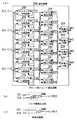
図13は、従来のクロックアンドデータリカバリ回路の構成を示す図である。基準クロック(Ref CLK)からPLL(Phase Locked Loop;位相同期ループ)の電圧制御発振器(Voltage Controlled Oscillator;VCO)51で互いに等間隔の位相差の多相クロック(Multiphase Output)を生成する。VCO51は、アナログ構成のリングオシレータ(反転回路を奇数段リング状に接続して発振器を構成する)よりなり、該リングオシレータを構成する各段の差動反転回路の出力から、等間隔の位相差の多相クロックが差動で取り出される。複数のフリップフロップ52(F/F1〜F/F8)は、入力データDATAをデータ端子に共通に入力し、VCO51から出力される多相クロックの各クロックをそれぞれクロック端子に入力し、データDATAをクロック信号の立ち上がり又は立ち下がりエッジでサンプルして出力し、複数のフリップフロップ52(F/F1〜F/F8)からそれぞれ出力される出力データを入力し、出力データが論理値をアップ、ダウンとしてカウントするカウンタ53と、カウンタ53の出力を所定の時定数にわたって時間平均するフィルタ55を備え、フィルタ55の出力電圧を電圧制御発振器(VCO)の制御電圧として供給し、フリップフロップ52の出力のうちの一部又はすべてと、VCO51から出力される1相のクロックとが、データとクロックとして出力される。複数のフリップフロップ52(F/F1〜F/F8)の出力は、データDATAを、少しずつ位相のずれたクロックでサンプルしたものであり、データDATAを、基準クロックの周波数の8倍の周波数でサンプルしたサンプリング波形が得られ、出力値が隣りのフリップフロップの出力値と不一致となるフリップフロップのクロックのタイミングが、データDATAの遷移点となる。
【0003】
データの遷移点に対してクロックが遅れている場合(ラッチタイミングが遅れる場合)、カウンタ53の値をアップさせて、クロックの位相を進め、データの遷移点に対してクロックが進んでいる場合(ラッチタイミングが進んでいる場合)、カウンタ53の値をダウンさせてクロックの位相を遅らせる制御が行われる。なお、カウンタ53は、複数のフリップフロップF/F1〜F/F8のそれぞれの出力値が論理0のとき、容量を定電流で充電し、論理1のとき容量を定電流で放電させるチャージポンプ(CP)で構成してもよい。
【0004】
図13に示したクロックアンドデータリカバリ回路の例としては、例えば文献1(ISSCC 1997 p.p 238−239 Alan Fiedler,"A 1.0625GHz Tranceiver with 2x−Oversampling and Transmit Siginal Preemphasis")が参照される。上記文献1に記載されるクロックアンドデータリカバリ回路は、シリアル入力データからクロックとデータをリカバしパラレルデータとして出力するレシーバ回路を備え、PLL(Phase Locked Loop;位相同期ループ)のVCO(電圧制御発振器)は10遅延段(10-delay-stage)のリングオシレータを有し、VCOの20のクロック位相は2xオーバサンプリングクロックをクロックとデータのリカバするレシーバ回路に与えており、レシーバ回路では、VCOを入力データにロックさせ、NRZ(Non Return to Zero)波形のデータの遷移からクロックをリカバしている。なお、上記文献1に記載されるクロックアンドデータリカバリ回路において、データ位相検出器(data phase detector)は、複数配置された高速ラッチと、高速ラッチ回路の一致/不一致を検出する排他的論理ゲートよりなり、データビットをサンプルするラッチは、VCOの正相クロックでクロッキングされ、データビット間のバウンダリ(境界;boundary)をサンプルするラッチは、VCOの逆相クロックでクロッキングされる構成とされている。
【0005】
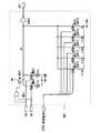
図14は、文献2(ISSCC 1997 p.p 332−333 S.Sidiropoulos and Mark Horowitz et al.,"A semi−digital delay locked loop with unlimited phase shift capability and 0.08-400MHz operating range")に記載されているDLL(遅延同期ループ)とインターポレータとの組み合わせからなるクロック制御回路の構成の一例を示す図である。図14を参照すると、DLL回路60において、入力クロックに同期した多相クロック信号P1〜Pnを出力し、多相クロック信号P1〜Pnはスイッチ20に入力され、スイッチ20で選択された隣り合う二つの信号がインターポレータ(位相インターポレータ)30に入力され、インターポレータ30で二つの信号の位相を内分した信号が出力OUTから出力される。制御回路40は、出力OUTと基準クロックとの位相差検出結果に基づき、インターポレータ30の内分比を可変制御するとともにスイッチ20の切り替えを制御する。
【0006】
図14のインターポレータ30(位相インターポレータ)は、図15に示すようなアナログ回路で構成されている。図15を参照すると、この位相インターポレータは、ソースが共通接続されて第1の定電流源CS1に接続され、ゲートにクロックIN1、IN1Bを差動で受け、出力対がそれぞれ第1の負荷の一端(並列接続されたPチャネルMOSトランジスタMP61、MP62の共通ドレイン)と第2の負荷の一端(並列接続されたPチャネルMOSトランジスタMP61、MP62の共通ドレイン)に接続され第1の差動対をなすNチャネルMOSトランジスタMN61、MN62と、ソースが共通接続されて第2の定電流源CS2に接続され、ゲートにクロックIN2、IN2Bを差動で受け出力対がそれぞれ第1の負荷の一端(並列接続されたPチャネルMOSトランジスタMP61、MP62の共通ドレイン)と第2の負荷の一端(並列接続されたPチャネルMOSトランジスタMP61、MP62の共通ドレイン)に接続され第2の差動対をなすNチャネルMOSトランジスタMN63、MN64と、を備え、第1、第2の差動対の共通接続された出力対から、二つの入力クロックの重み付き和の位相の出力OUT、OUTBを出力する。この位相インターポレータにおいて、デジタル重みコードictlを(16ビットb[0]〜b[15])が第1、第2の定電流源CS1、CS2に供給されており、第1、第2の定電流源CS1、CS2の電流値を可変させ(16ビットb[0]〜b[15]をゲート端子に入力するNチャネルMOSトランジスタMN6A1〜MN6A15のオン、オフで定電流源トランジスタMN6B1〜MN6B15の個数が選択され電流値が可変される)、出力クロックの位相に変換している。
【0007】
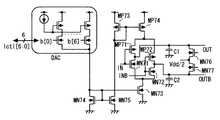
また文献3(ISSCC1999 p.p 180-181 "A2BPararell 1.25Gb/s Interconnect I/O interface with Self Configurable Link and Plesiochronous Clocking")には、位相インターポレータとして、図16に示すような構成が開示されている。図16を参照すると、制御信号Ictlに応じた出力電流を出力する電流出力型のデジタルアナログ変換器(DAC)と、DACの出力電流を第1のカレントミラー回路(MN74、MN75)で折り返し、折り返した電流を第2のカレントミラー回路(MP73、MP74)で受け、その出力ミラー電流を、差動クロック入力IN、INBを入力とする差動対回路に対して供給し、第1のカレントミラー回路(MN74、MN75)の第2の出力端をなす定電流源トランジスタMN73から差動対回路に電流を供給し、差動対回路の出力からはクロックINを位相シフトしたクロックOUT、OUTBが出力される。なお、差動対回路において、共通接続されたソースが定電流源トランジスタMP73に接続され、ゲートに差動クロック対IN、INBが入力されるNチャネルMOSトランジスタMN71、MN72と、ソースが共通接続されて第2のカレントミラー回路の出力トランジスタMP74のドレインに接続され、ゲートに差動クロック対IN、INBを入力とし、ドレインがそれぞれNチャネルMOSトランジスタMN71、MN72のドレインに接続されたPチャネルMOSトランジスタMP71、MP72を有し、NチャネルMOSトランジスタMN71、MN72のドレインから出力OUT、OUTBが取り出される。NチャネルMOSトランジスタMN71、MN72のドレインとグランド間にはそれぞれ容量C1、C2が接続されており、またNチャネルMOSトランジスタMN71、MN72のドレイン間には、NチャネルMOSトランジスタMN76、MN77が直列に接続され、NチャネルMOSトランジスタMN76、MN77がオンのとき、出力OUT、OUTBは中間電位VDDに充電される。
【0008】
図16において、クロックINがHighレベルに遷移すると、NチャネルMOSトランジスタMN71がオンし、NチャネルMOSトランジスタMN72がオフし、PチャネルMOSトランジスタMP71がオフし、PチャネルMOSトランジスタMP72がオンし、容量C1は放電され、容量C2は充電され、出力OUTはLowレベル、出力OUTBはHighレベルに遷移し、クロックINがLowレベルに遷移すると、MOSトランジスタMN71がオフし、NチャネルMOSトランジスタMN72がオンし、PチャネルMOSトランジスタMP72がオフし、PチャネルMOSトランジスタMP71がオンし、容量C1は充電され、容量C2は放電され、出力OUTはHighレベル、出力OUTBはLowレベルに遷移し、デジタルアナログ変換器(DAC)に供給する制御信号Ictlによってクロックの帯域が可変制御される。
【0009】
以上、図13、図15を参照して説明したように、上記従来の回路においては、多相クロックをVCO回路で生成しており、またインターポレータとしては、アナログ回路よりなる位相インターポレータが用いられている。
【0010】
また図16に示したように、アナログ位相インターポレータの帯域制御を電流源に流す電流で制御しており、複数の周波数帯に対応するには、定電流源の出力電流範囲を広げる等の対策を施すことが必要とされている。この場合、位相インターポレータのリニアリティを補償して、定電流源の出力電流範囲を広げることは、必ずしも容易とはいえない。
【0011】
【発明が解決しようとする課題】
したがって、本発明が解決しようとする課題は、周波数範囲の変更を容易化し、特性の調整を容易化するクロックアンドデータリカバリ回路及び方法を提供することにある。本発明の他の課題は、データ及びクロックの並列数を可変自在とするクロックアンドデータリカバリ回路及び方法を提供することにある。
【0012】
【課題を解決するための手段】
上記課題を解決するための手段を提供する本発明は、入力データを共通に入力とする複数のラッチ回路を備え、前記複数のラッチ回路は、前記複数のラッチ回路にそれぞれ供給される互いに位相がずれているクロックの遷移エッジで前記入力データをサンプルして出力し、前記複数のラッチ回路の出力から前記入力データの遷移点のクロックに関する位相を検出して出力する位相検出回路と、前記位相検出回路の出力を平滑化するフィルタと、前記フィルタの出力に基づき前記クロックの位相を制御する回路と、を備え、前記入力データからクロックとデータを復元するクロックアンドデータリカバリ回路において、前記複数のラッチ回路にそれぞれ互いに位相がずれているクロックを供給する回路が、互いに位相の異なる複数のクロック(「多相クロック」という)を入力とし前記多相クロックの中からクロック対を複数組選択して出力するスイッチと、前記スイッチから出力される複数組のクロック対を入力とし該クロック対の位相差を内分した時間で遅延時間が規定される信号を出力する複数のインターポレータと、を備え、前記各インターポレータは、入力するクロック対の論理値に応じて、容量の充電パスと放電パスをそれぞれオン及びオフさせる回路と、前記容量の端子電圧としきい値との大小関係が反転したときに出力論理値を可変させるバッファ回路と、を備え、さらに、前記容量の容量値が制御信号によってオン及びオフされるスイッチ群により可変に設定される構成とされており、前記複数のインターポレータから出力される信号が、前記複数のラッチ回路のクロックとして供給され、前記クロックの位相を制御する回路が、前記フィルタの出力をデコードするデコーダを備え、前記デコーダの出力信号に基づき、前記スイッチにおけるクロック対の選択の切替えが制御されるとともに、前記インターポレータの内分比が可変に設定されることで、前記複数のラッチ回路に供給されるクロックの位相が可変される。以下の説明からも明らかとされるように、上記課題は本願特許請求の範囲の各請求項の発明によっても同様にして解決される。
【0013】
【発明の実施の形態】
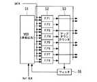
本発明の実施の形態について説明する。本発明のクロックアンドデータリカバリ(clock and data recovery)回路は、その好ましい一実施の形態において、図1及び図2を参照すると、互いに位相の異なる複数のクロックを入力し、複数のクロックから複数組のクロック対を選択出力するスイッチ110と、スイッチ110から出力されるクロック対をそれぞれ入力とし該クロック対の位相差を所定の内部比で内分した時間で遅延時間が規定される出力クロックを出力するインターポレータ111(INT1〜INT8)を複数備えてなる位相シフト回路101と、複数のインターポレータから出力されるクロック(CLK1〜CLK8)の立ち上がり又は立ち下がりエッジで入力データをサンプルする複数のラッチ回路102(F/F1〜F/F8)と、複数のラッチ回路102(F/F1〜F/F8)の出力がアップを示すかダウンを示すかでカウント値をアップ・ダウンするカウンタ103と、カウンタ103の出力を時間平均するフィルタ105と、フィルタ105の出力をデコードするデコーダ106と、を備えている。各部の構成と動作の概略を以下に説明する。
【0014】
インターポレータ111(INT1〜INT8)は、入力するクロック対の値に基づき、容量の充電パスと放電パスをそれぞれオン及びオフさせる回路(図4の遅延が可変されるCMOS型のインバータINV1とINV2)と、前記容量の端子電圧としきい値との大小関係が反転したときに出力論理値を可変させるバッファ回路(図4のINV3)を備え、出力信号の位相が可変に設定され、さらに、容量の容量値が、容量値決定用の制御信号(図4のCnt[0:7])によって、オン及びオフ制御されるスイッチ群(図4のMNA1〜MNA8)により可変に設定される構成とされており、広い周波数範囲に対応可能としている。
【0015】
カウンタ103は、複数のラッチ回路(F/F1〜F/F8)102の出力に基づき、充電パスをオンして容量を充電し、又は放電パスをオンして容量の電荷を放電する(結果として蓄積電荷の加算又は減算を行う)チャージポンプで構成してもよいし、あるいは、アップ・ダウンカウンタ、加算器等のデジタル回路で構成してもよい。フィルタ105は、アナログ回路の低域通過フィルタ、もしくはデジタルフィルタ(平均化フィルタ)よりなる。
【0016】
デコーダ106から出力される切替信号Uに基づき、スイッチ110のクロック対の組み合わせが切り換えられ、デコーダ106から出力される制御信号Sに基づき、複数のインターポレータ111の内分比が可変に設定され、複数のインターポレータ111から出力されるクロックの位相が可変に制御される。
【0017】
本発明の一実施の形態においては、複数のラッチ回路102(フリップフロップF/F1〜F/F8)から出力される出力データと、位相シフト回路101から出力されるクロック(例えば1相クロック)との組が、セレクタ(選択回路)104に入力され、任意の組が選択出力され、データ及びクロック出力の並列数が可変自在とされている。
【0018】
【実施例】
上記した本発明の実施の形態についてさらに詳細に説明すべく、本発明の実施例について以下に説明する。図1(a)は、本発明の一実施例の構成を示す図である。図1(a)を参照すると、本発明のクロックアンドデータリカバリ回路の一実施例は、8相クロックを入力し、位相をシフトさせた8組のクロックを出力する位相シフト回路101と、位相シフト回路101から出力されるクロックをクロック入力端に入力し、入力データDATAをデータ入力端に入力し、入力データDATAを、クロックの立ち上がりエッジでサンプルする複数のD型フリップフロップ102(F/F1〜F/F8)と、複数のD型フリップフロップ102の出力が論理0のときアップ信号とし、論理1のときダウン信号としてカウント値をアップ/ダウンさせるカウンタ103と、カウンタ103の出力を時間平均するフィルタ105と、フィルタ105の出力をデコードするデコーダ106と、位相シフト回路101から出力される1相クロックと複数のD型フリップフロップ102(F/F1〜F/F8)の出力データとの各組を入力し、選択制御信号に基づき、選択された組(1相クロックとサンプルされた出力データ)を並列出力するセレクタ(選択回路)104と、を備えている。なお、図1(a)において、セレクタ104には、複数のD型フリップフロップ102(F/F1〜F/F8)のうち、F/F1、F/F3、F/F5、F/F7の出力が入力されているが、F/F1〜F/F8すべての出力を入力する構成としてもよい。
【0019】
複数のD型フリップフロップ102(F/F1〜F/F8)は、位相シフト回路101から出力されるクロックCLK1〜CLK8の、立ち上がりエッジ(又は立ち下がりエッジ)で入力データDATAをサンプル出力する(図1(b)参照)。複数のD型フリップフロップ102(F/F1〜F/F8)の出力(例えば“00001111”)からは、クロック周期の1/8のサンプリング周期で入力データをサンプリングした波形データが得られ、隣り合うD型フリップフロップ102の出力値の変化点で入力データが遷移している。カウンタ103は、複数のD型フリップフロップ102の出力をカウントし、カウント値をフィルタ105により所定の時定数で平滑化した信号により、複数のD型フリップフロップ102に供給されるクロックの位相を進ませるか遅らせるかの制御が行われ、入力データDATAにロックしたクロックとデータが出力される。
【0020】
図2は、本発明の一実施例の位相シフト回路101の構成を示す図である。図2を参照すると、位相シフト回路101は、8相クロック(8 phase CLK)を入力とするスイッチ110と、スイッチ110から出力されるクロック対を入力する8個のインターポレータ111(INT1〜INT8)を備えている。スイッチ110は、例えばロータリスイッチとして構成され、デコーダ回路からの出力に基づき、出力クロック対の組み合わせを切り換える。
【0021】
図3は、図2に示したスイッチ110(ロータリスイッチ)とインターポレータ111の構成の一例を示す図である。図3を参照すると、このロータリスイッチは、8相のクロックP0〜P7のうちの奇位相クロック(P0、P2、P4、P6)を入力して各インターポレータ111に選択出力する第1のスイッチ110−1と、多相クロックP0〜Pnのうちの偶位相クロック(P1、P3、P5、P7)を入力して各インターポレータ111に選択出力する第2のスイッチ110−2と、を備えている。初期状態(デコーダ106による切替制御が行われていない状態)において、例えばインターポレータ1111〜1118には、第1のスイッチ110−1及び第2のスイッチ110−2より出力される、クロック対(P0、P1)、(P1、P2)、(P2、P3)、(P3、P4)、(P4、P5)、(P5、P6)、(P6、P7)、(P7、P0)がそれぞれ入力される。
【0022】
デコーダ106は、各インターポレータ1111〜1118に制御信号S、SBを出力するとともに、インターポレータ1111〜1118の位相差の内分比(内分比とは、後述する図4のw:1−w)が上限又は下限に達した場合において、さらに位相を進めるか遅らせる必要がある場合には、当該インターポレータ1111〜1118に供給するクロック対の組み合わせを切替えるための切替信号Uをスイッチ110−1、110−2に出力する。例えばインターポレータ1111〜1118にクロック対の組み合わせ(P0、P1)、(P1、P2)、(P2、P3)、(P3、P4)、(P5、P6)、(P6、P7)、(P7、P0)が供給されている場合、クロック対の組み合わせを切替えてクロックの位相を遅らせる場合、インターポレータ1111〜1118に、(P1、P2)、(P2、P3)、(P3、P4)、(P5、P6)、(P6、P7)、(P7、P0)、(P0、P1)を供給するように切替える。スイッチ110は、クロック対の組み合わせを回転(rotate)するため「ロータリスイッチ」という。
【0023】
図4は、図2に示したインターポレータ111の構成を示す図である。図5は、図4のインターポレータの動作を示す図である。図4及び図5を参照すると、このインターポレータは、第1の入力IN1と、第2の入力IN2の位相差がTの場合、二つの入力にIN1を入力した遅延時間の出力信号とOUT1と二つの入力にIN2を入力した遅延時間の出力信号とOUT2の間をw:1−wで内分した時間で規定される遅延時間の出力OUTが出力される。インターポレータは、入力IN1、入力IN2を受け、遅延時間が可変されるCMOS型のインバータINV1、INV2と、インバータINV1、INV2の出力の共通接続点(ノードN1)を入力するインバータ3と、ノードN1とグランド間に直列に接続される、NチャネルMOSトランジスタ(MNA1〜MNA8)と容量(C0〜C7)とを備え、NチャネルMOSトランジスタ(MNA1〜MNA8)のゲートに入力される制御信号Cnt[0:7]により、NチャネルMOSトランジスタ(MNA1〜MNA8)がオン、オフされ、ノードN1に付加される容量値が決定される。なお、容量C0〜C7の容量値は、C0を基準に、例えば2倍、4倍、8倍、16倍と2のべき乗等に設定してもよい。この場合、NチャネルMOSトランジスタ(MNA1〜MNA8)のW/L比(ゲート幅)も、対応する容量の容量値に応じたサイズとされる。
【0024】
制御信号Cnt[0:7]は、クロック信号の周波数を検知する周波数検知回路からの出力で設定してもよいし、あるいは、アプリケーションに応じて、レジスタ、ディップスイッチ等を所望の値に設定することで、制御信号Cnt[0:7]を決定してもよい。制御信号Cnt[0:7]により、ノードN1に付加される容量値を可変させることで、対応可能な周波数範囲を拡大することができる。
【0025】
図6は、図2に示したインターポレータ111のトランジスタレベルでの具体的構成の一例を示す図である。図6を参照すると、このインターポレータは、電源VDDと内部ノードN51間に接続され、入力IN1とIN2を入力とする論理和回路OR51からの出力信号がLowのとき、オンされるPチャネルMOSトランジスタMP51を備え、内部ノードN51とグランド間には、NチャネルMOSトランジスタと容量の直列回路が複数本並列に接続されており(MN51とC1、…、MN58とC8)、内部ノードN51が入力端に接続され、出力端から出力信号OUTが取り出されるインバータINV51と、を備えている。NチャネルMOSトランジスタMN51〜MN58のゲートに接続される制御信号Cnt[0:7]は、クロック信号の周波数を検知する周波数検知回路(図示されない)からの出力で設定してもよいし、あるいは、アプリケーションに応じて、レジスタ、ディップスイッチ等を所望の値に設定することで、制御信号Cnt[0:7]を決定してもよい。制御信号Cnt[0:7]により、ノードN51に付加される容量値を可変させることで、対応可能な周波数範囲を拡大することができる。
【0026】
内部ノードN51にドレインが接続され、互い並列に接続された2N個のNチャネルMOSトランジスタMN11〜MN1N、MN21〜MN2Nと、2N個のNチャネルMOSトランジスタMN11〜MN1N、MN21〜MN2Nのソースにドレインがそれぞれ接続され、ソースがグランドに接続された2N個のNチャネルMOSトランジスタMN31〜MN3N、MN41〜MN4Nと、を備え、2N個のNチャネルMOSトランジスタのうちの片側半分の、N個のNチャネルMOSトランジスタMN11〜MN1Nのゲートには、入力信号IN1が共通に接続され、2N個のNチャネルMOSトランジスタのうちもう半分の、N個のNチャネルMOSトランジスタMN21〜MN2Nのゲートには、入力信号IN2が共通に接続されている。
【0027】
NチャネルMOSトランジスタMN31〜MN3N、MN41〜MN4Nのゲートに入力される制御信号(Nビット制御コード)S[0]〜S[N−1]、制御信号(Nビット制御コード)SB[0]〜SB[N−1]により、NチャネルMOSトランジスタMN31〜MN3NとNチャネルMOSトランジスタMN41〜MN4Nのうちの所定個数がオンとされる。Nビットの制御信号S[0:N−1]、SB[0:N−1]は、デコーダ106から入力され、SB[0]〜SB[N−1]は、S[0]〜S[N−1]をそれぞれインバータ(図3のインターバINV)で反転した相補の信号で与えられる。
【0028】
図6を参照して、このインターポレータの動作について説明する。入力IN1、IN2がLowレベルのときOR回路51の出力をゲートに入力とするPチャネルMOSトランジスタMP51はオンし、電源からの電流で容量C(容量値は、容量C1〜C8のうち制御信号Cntでオンに設定されているNチャネルMOSトランジスタMN51〜MN58に接続する容量の合成容量値)を充電する。
【0029】
そして、入力IN1に印加される信号がLowレベルからHighレベルへの立ち上がり遷移時に、NチャネルMOSトランジスタMN11〜MN1Nがオンし、ドレインがNチャネルMOSトランジスタMN11〜MN1Nのソースに接続され、ソースがグランドに接続され、ゲートに、制御信号S[0]〜S[N−1]がそれぞれ入力されるNチャネルMOSトランジスタMN31〜MN3Nのうち、制御信号でオンとされているn個のNチャネルMOSトランジスタのパスを介して、容量Cの蓄積電荷が一部放電される。
【0030】
入力IN1の立ち上がり遷移から遅れて入力IN2がLowレベルからHighレベルへの立ち上がる時に、NチャネルMOSトランジスタMN21〜MN2Nがオンし、ドレインがNチャネルMOSトランジスタMN21〜MN2Nのソースに接続され、ソースがグランドに接続され、ゲートに制御信号SB[0]〜SB[N−1]が入力されるNチャネルMOSトランジスタMN41〜MN4Nのうち、制御信号でオンとされている(N−n)個のNチャネルMOSトランジスタのパスを介して、容量Cの蓄積電荷が放電される。
【0031】
容量Cの端子電圧を入力するインバータINV51の出力がHighレベルに反転するまでに放電される電荷をCVとすると、入力IN1がHighレベルへの遷移してから位相差(T)の間、電流nIで放電し、つづいて、入力IN2がHighレベルへの遷移し、n個のNチャネルMOSトランジスタMN11〜MN1nと,(N−n)個のNチャネルMOSトランジスタMN21〜MN2(N−n)の計N個のNチャネルMOSトランジスタのドレイン電流NIで放電され、入力IN2のLowからHighレベルへの立ち上がりから出力OUTの立ち上がりまでの遅延時間は、
(CV−n・I・T)/NI=CV/NI−n・T/N …(1)
と表され、入力IN1とIN2の位相差TのN分割を単位として遅延時間を可変することができる。
【0032】
本発明において、多相クロックは、PLLの電圧制御発振器(VCO)から生成してもよい。この場合、VCOのリングオシレータの所定の段の反転回路からクロックが取り出される。あるいは、多相クロックは、多相クロック逓倍回路で生成してもよい。
【0033】
図7は、位相シフト回路101に供給する多相クロックを、逓倍用インターポレータ(多相クロック逓倍回路)を用いた多相クロック発生回路200を用いて生成する構成を示したものである。図1の位相シフト回路101は、多相クロック発生回路200と、ロータリスイッチ110から構成されており、インターポレータ1111〜111nから出力されるクロックCLK1〜CLKn(ただし、nは8)は、図1のD型フリップフロップ102(F/F1〜F/F8)のクロック入力端にそれぞれ供給される。図7において、クロック1としては、水晶発振回路等のクロック生成回路から生成された基準クロックが用いられる。
【0034】
図8は、図7の多相クロック発生回路200として構成の一例として、4相クロックを生成する4相クロック逓倍回路の構成の具体例を示す図である。図8に示すように、この4相クロック逓倍回路は、入力クロック205を4分周し4相クロックQ1〜Q4を出力する1/4分周器201と、n段縦続接続された4相クロック逓倍回路(MPFD(multiphase frequency doubler;多相倍周回路)ともいう)2021〜202nと、周期検知回路204とを備えている。最終段の4相クロック逓倍回路202nからは、2n逓倍された4相クロックQn1〜Qn4が出力される。なお、4相クロック逓倍回路の段数nは任意である。この4相クロック逓倍回路の動作の概略を述べれば、4相のクロックを、各4相クロック逓倍回路202で、8相にした後、4相に戻すことで、連続的に逓倍を行う。なお、最終段の4相クロック逓倍回路202nから生成された8相のクロック(図10のP21〜P28)をそのまま出力する構成としてもよい。詳細を以下に説明する。
【0035】
図9は、図8に示した、多相クロック逓倍回路を4相クロック逓倍回路とした場合の、4相クロック逓倍回路202nの構成の一例を示す図である。なお、図8に示した4相クロック逓倍回路2021〜202nは、いずれも同一構成とされる。
【0036】
図9(a)を参照すると、この4相クロック逓倍回路202nは、8組のタイミング差分割回路208〜215と、8個のパルス補正回路216〜223と、4組の多重化回路224〜227から構成されている。すなわち、4相のクロック(Q(n-1)1〜Q(n-1)4)を入力し、二つの入力のタイミング差を分割した信号を出力する8個のタイミング差分割回路208〜215を備え、奇数番目のタイミング差分割回路208、210、212、214は、二つの入力としてn相のクロックのうち同一クロック(Q(n-1)1とQ(n-1)1、Q(n-1)2とQ(n-1)2、Q(n-1)3とQ(n-1)3、Q(n-1)4とQ(n-1)4)をそれぞれ入力とし、偶数番目のタイミング差分割回路209、211、213、215は、n相のクロックのうち隣り合うクロック対(Q(n-1)1とQ(n-1)2、Q(n-1)2とQ(n-1)3、Q(n-1)3とQ(n-1)4、Q(n-1)4とQ(n-1)1)を入力としている。
【0037】
J番目(ただし、1≦J≦8)のパルス幅補正回路は、J番目のタイミング差分割回路の出力を第1の入力とし、((J+2) mod n)番目(ただし、(J+2) mod nは、(J+2)をnで割った余り)のタイミング差分割回路の出力を第2の入力とし、K番目(ただし、1≦K≦4)の多重化回路は、K番目のパルス幅補正回路の出力と(K+n)番目のパルス幅補正回路の出力とを入力とする。図9(b)は、パルス幅補正回路の構成を示す図であり、第2の入力T23をインバータINVで反転した信号と、第1の入力T21を入力とするNAND回路からなる。図9(c)は、多重化回路の構成を示す図であり、2入力NAND回路からなる。
【0038】
図10は、図9に示した4相クロック逓倍回路202のタイミング動作を示す信号波形図である。クロックT21の立ち上がりは、クロックQ(n−1)1の立ち上がりからタイミング差分割回路208の内部遅延分の遅れで決定され、クロックT22の立ち上がりは、クロックQ(n−1)1の立ち上がりとクロックQ(n−1)2の立ち上がりのタイミングのタイミング差分割回路209でのタイミング分割と内部遅延分の遅れで決定され、クロックT23の立ち上がりは、クロックQ(n−1)1の立ち上がりとクロックQ(n−1)2の立ち上がりのタイミングのタイミング差分割回路210でのタイミング分割と内部遅延分の遅れで決定され、以下同様にして、クロックT26の立ち上がりはクロックQ(n−1)3の立ち上がりとクロックQ(n−1)4の立ち上がりのタイミングのタイミング差分割回路213でのタイミング分割と内部遅延分の遅れで決定され、クロックT27の立ち上がりはクロックQ(n−1)4の立ち上がりのタイミングのタイミング差分割回路214での内部遅延分の遅れで決定され、クロックT28の立ち上がりはクロックQ(n−1)4の立ち上がりとクロックQ(n−1)1の立ち上がりのタイミングのタイミング差分割回路215でのタイミング分割と内部遅延分の遅れで決定される。
【0039】
タイミング差分割回路208と210から出力されるクロックT21とT23はパルス幅補正回路216に入力され、パルス幅補正回路216では、クロックT21で決定される立ち下がりエッジ、クロックT23で決定される立ち上がりエッジを有するパルスP21を出力する。同様の手順で、パルスP22〜P28が生成され、クロックP21〜P28は位相が45度ずつずれたデューティ25%の8相のパルス群となる。このクロックP21と位相が180度ずれたクロックP25は、多重化回路224で多重化反転され、デューティ25%のクロックQn1として出力される。同様にして、クロックQn2〜Qn4が生成される。クロックQn1〜Qn4は、位相が90度ずつずれたデューティ50%の4相のパルス群となり、クロックQn1〜Qn4の周期は、クロックQ(n−1)1〜Q(n−1)4からクロックQn1〜Qn4を生成する過程で、周波数が2倍に逓倍される。
【0040】
すなわち、4相のクロックQ(n−1)1〜Q(n−1)4から8相クロックP21〜P28を生成し、倍周の4相クロックQn1〜Qn4を生成している。なお、最終段の4相クロック逓倍回路202nから(図8参照)において、8相クロックP21〜P28を出力する構成としてもよい。
【0041】
図11は、図9に示したタイミング差分割回路208、209の動作原理を模式的に示す図であり、同一の信号を入力とするタイミング差分割回路208、210、212、214(homo)では、固有の遅延時間で出力信号を出力し、位相差Tのある2入力を入力とするタイミング差分割回路209、211、213、215(hetero)は、タイミング差分割回路の固有の遅延時間に、位相差Tを2等分した時間T/2(位相差Tを等分した時間)を加算した遅延時間で遷移する信号を出力する。
【0042】
図12は、図9に示したタイミング差分割回路208、209の構成の一例を図である。タイミング差分割回路208では、二つの入力IN1、IN2に、同一信号が入力され、タイミング差分割回路209では、隣り合う二つの信号が入力されている。すなわち、タイミング差分割回路208では、同一入力Q(n−1)1が入力端IN1、IN2に入力され、タイミング差分割回路209では、Q(n−1)1とQ(n−1)2が入力端IN1、IN2に入力されている。電源VDDにソースが接続されドレインが内部ノードN1に接続されたPチャネルMOSトランジスタMP01と、入力信号IN1、IN2を入力し、出力がPチャネルMOSトランジスタMP01のゲートに接続されたOR回路OR1と、内部ノードN1にドレインが接続され、ソースが定電流源I0を介してグランドに接続され、ゲートに入力信号IN1、IN2が接続されたNチャネルMOSトランジスタMN01、MN02を備え、内部ノードN1は、インバータINV01の入力端に接続され、内部ノードN1とグランド間には、NチャネルMOSトランジスタMN11と容量CAP11を直列接続した回路、NチャネルMOSトランジスタMN12と容量CAP12を直列接続した回路、…、NチャネルMOSトランジスタMN15と容量CAP15を直列接続した回路が、並列に接続され、各NチャネルMOSトランジスタMN11、MN12、…、MN15のゲートには、入力クロックの周期を検知する周期検知回路204からの、5ビット幅の制御信号206がそれぞれ接続されてオン・オフ制御される。NチャネルMOSトランジスタMN11、MN12、MN13、MN14、MN15のゲート幅と容量CAP11、CAP12、CAP13、CAP14、CAP15は、そのサイズ比が、例えば16:8:4:2:1とされており、周期検知回路204(図8参照)から出力される制御信号206に基づき、共通ノードに接続される負荷を32段階に調整することで、クロック周期が設定される。
【0043】
タイミング差分割回路208については、二つの入力IN1、IN2に共通入力されるクロックQ(n−1)1の立ち上がりエッジにより、ノードN1の電荷が二つのNチャネルMOSトランジスタMN01、MN02を介して引き抜かれ、ノードN1の電位がインバータINV01のしきい値に達したところで、インバータINV01の出力であるクロックT21が立ち上がる。インバータINV01のしきい値に達したところまで引き抜く必要のあるノードN1の電荷をCV(ただし、Cは容量値、Vは電圧)とし、NチャネルMOSトランジスタによる放電電流をIとすると、クロックQ(n−1)1の立ち上がりから、CVの電荷量を、電流値2Iの定電流で放電することになり、その結果、時間CV/2Iが、クロックQ(n−1)1の立ち上がりエッジから、クロックT21の立ち上がりまでのタイミング差(伝搬遅延時間)を表している。
【0044】
クロックQ(n−1)1がLowレベルのとき、PチャネルMOSトランジスタMP01がオンとされ、ノードN1がHighに充電され、インバータINV01の出力クロックT21はLowレベルとなる。
【0045】
タイミング差分割回路209については、クロックQ(n−1)1の立ち上がりエッジから時間tCKn(=多相クロック周期)後の期間、ノードN1の電荷が引き抜かれ、時間tCKn後、クロックQ(n−1)2の立ち上がりエッジから、ノードN1の電位がインバータINV01のしきい値に達したところで、クロックT22のエッジが立ち上がる。ノードN1の電荷をCVとし、NMOSトランジスタの放電電流をIとすると、クロックQ(n−1)1の立ち上がりから、CVの電荷量をtCKnの期間、定電流Iで放電し、残りの期間を、定電流2Iで引き抜く結果、時間、
tCKn+(CV−tCKn・I)/2I=CV/2I+tCKn/2 …(2)
が、クロックQ(n−1)1の立ち上がりエッジから、クロックT22の立ち上がりエッジのタイミング差を表している。
【0046】
すなわち、クロックT22とクロックT21の立ち上がりのタイミング差は、tCKn/2となる。
【0047】
クロックQ(n−1)1とQ(n−1)2がともにLowレベルとなり、ノードN1が、PチャネルMOSトランジスタMP01を介して電源からHighレベルに充電された場合、クロックT22が立ち下がる。クロックT22〜T28についても同様とされ、クロックT21〜T28の立ち上がりのタイミング差はそれぞれtCKn/2となる。
【0048】
パルス幅補正回路216〜223は、位相が45度ずつずれたデューティ25%の8相のパルス群P21〜P28を生成する(図9、図10参照)。
【0049】
多重化回路224〜227は、位相が90度ずつずれたデューティ50%の4相のパルス群Qn1〜Qn4を生成する(図9、図10参照)。
【0050】
図12に示したタイミング差分割回路は、使用されるアプリケーションに応じて、適宜、変形される。例えば、PチャネルMOSトランジスタMP01のゲートに、第1、第2の入力信号IN1、IN2を入力とする否定論理積回路(NAND)の出力信号を入力し、第1の入力信号IN1、第2の入力信号IN2をインバータでそれぞれ反転した信号をNチャネルMOSトランジスタMN01、MN02のゲートに入力する構成としてもよい。この場合、第1、第2の入力信号IN1、IN2がHighレベルのとき、PチャネルMOSトランジスタMP01がオン(導通)して内部ノードN1が充電され、インバータINV01の出力はLowレベルとされ、第1、第2の入力信号IN1、IN2の一方又は両方がLowレベルのとき、PチャネルMOSトランジスタMP01がオフしPチャネルMOSトランジスタMN01とMN02の一方又は両方がオンし、内部ノードN1が放電され、内部ノードN1の電圧がインバータINV01のしきい値以下に下がった場合、インバータINV01の出力は立ち上がりHighレベルとなる。
【0051】
【発明の効果】
以上説明したように、本発明によれば、従来の回路に較べて、周波数範囲の変更を容易化し、特性の調整を容易化する、という効果を奏する。その理由は、本発明においては、多相クロックの位相をシフトさせて出力する位相シフト回路を構成するインターポレータの内部ノードに付加される容量値を可変させることで周波数の変更に対応可能としているためである。
【0052】
また、本発明によれば、選択回路を設け、クロックアンドデータリカバリ回路の並列数を可変に切替えることができるという利点も有する。
【図面の簡単な説明】
【図1】本発明の一実施例の構成を示す図である。
【図2】本発明の一実施例の位相シフト回路の構成を示す図である。
【図3】本発明の一実施例の位相シフト回路におけるスイッチの構成を示す図である。
【図4】本発明の一実施例の位相シフト回路におけるインターポレータの構成を示す図である。
【図5】本発明の一実施例の位相シフト回路におけるインターポレータの動作原理を説明するタイミング波形図である。
【図6】本発明の一実施例の位相シフト回路におけるインターポレータの構成の一例を示す図である。
【図7】本発明の一実施例において位相シフト回路の入力に多相クロック発生回路の出力を用いた場合の構成の一例を示す図である。
【図8】本発明の一実施例の多相クロック発生回路の構成を示す図である。
【図9】本発明の一実施例における多相クロック発生回路を構成する4相クロック逓倍回路の構成を示す図である。
【図10】本発明の一実施例における4相クロック逓倍回路のタイミング動作を示す図である。
【図11】本発明の一実施例における4相クロック逓倍回路のインターポレータの動作を説明する図である。
【図12】本発明の一実施例における4相クロック逓倍回路のインターポレータの構成の一例を示す図である。
【図13】従来のクロックアンドリカバリ回路の構成の一例を示す図である。
【図14】従来のクロック制御回路の構成を示す図である。
【図15】従来の位相インターポレータの構成を示す図である。
【図16】従来の位相インターポレータの構成を示す図である。
【符号の説明】
1 クロック
20 スイッチ
30 インターポレータ
40 制御回路
51 VCO
52 フリップフロップ
53 アップダウンカウンタ
55 フィルタ
60 DLL
101 位相シフト回路
102 フリップフロップ
103 アップダウンカウンタ
104 セレクタ
105 フィルタ
106 デコーダ
110 スイッチ
111 インターポレータ
200 多相クロック発生回路
201 1/4分周回路
202 4相クロック逓倍回路
204 周期検知回路
205 クロック
206 制御信号
208〜215 タイミング差分割回路
216〜223 パルス幅補正回路
224〜227 多重化回路[0001]
BACKGROUND OF THE INVENTION
The present invention relates to a clock and data recovery circuit and method.
[0002]
[Prior art]
FIG. 13 is a diagram showing a configuration of a conventional clock and data recovery circuit. A voltage controlled oscillator (Voltage Controlled Oscillator: VCO) 51 of a PLL (Phase Locked Loop) is used to generate a multiphase clock (Multiphase Output) having a phase difference of equal intervals from the reference clock (Ref CLK). The
[0003]
When the clock is delayed with respect to the data transition point (when the latch timing is delayed), the value of the
[0004]
As an example of the clock and data recovery circuit shown in FIG. 13, Reference 1 (ISSCC 1997 pp 238-239 Alan Fiedler, “A 1.0625 GHz Tranceiver with 2x—Oversampling and Transmit Signal Preemphasis”) is referred to, for example. The clock and data recovery circuit described in
[0005]
FIG. 14 shows a DLL described in Reference 2 (ISSCC 1997 pp 332-333 S. Sidiropoulos and Mark Horowitz et al., “A semi-digital delay locked loop with unlimited phase shift capability and 0.08-400 MHz operating range”). It is a figure which shows an example of a structure of the clock control circuit which consists of a combination of (delay locked loop) and an interpolator. Referring to FIG. 14, the
[0006]
The interpolator 30 (phase interpolator) shown in FIG. 14 includes an analog circuit as shown in FIG. Referring to FIG. 15, in this phase interpolator, the sources are connected in common and connected to the first constant current source CS1, the gates receive the clocks IN1 and IN1B differentially, and the output pairs each have a first load. And a first differential pair connected to one end of the second load (common drain of the P channel MOS transistors MP61 and MP62 connected in parallel) and one end of the second load (common drain of the P channel MOS transistors MP61 and MP62 connected in parallel). N-channel MOS transistors MN61 and MN62 having a source connected in common to the second constant current source CS2, and receiving gates IN2 and IN2B differentially at their gates and each output pair having one end of a first load ( A common drain of P-channel MOS transistors MP61 and MP62 connected in parallel) and one end of the second load (parallel connection) N-channel MOS transistors MN63 and MN64 that are connected to the common drain of the P-channel MOS transistors MP61 and MP62 and form a second differential pair, and the first and second differential pairs are connected in common. From the output pair, outputs OUT and OUTB having a weighted sum of two input clocks are output. In this phase interpolator, the digital weight code ictl (16 bits b [0] to b [15]) is supplied to the first and second constant current sources CS1 and CS2, and the first and second constant current sources CS1 and CS2 are supplied. N-channel MOS transistor MN6A that varies the current values of constant current sources CS1 and CS2 (16 bits b [0] to b [15] are input to the gate terminals)1 ~ MN6A15 ON / OFF of constant current source transistor MN6B1 ~ MN6B15 Is selected and the current value is varied), and converted to the phase of the output clock.
[0007]
Reference 3 (ISSCC 1999 pp 180-181 “A2BPararell 1.25 Gb / s Interconnect I / O interface with Self Configurable Link and Plesiochronous Clocking”) discloses a configuration as shown in FIG. 16 as a phase interpolator. . Referring to FIG. 16, a current output type digital-to-analog converter (DAC) that outputs an output current corresponding to the control signal Ictl and the output current of the DAC are folded back by the first current mirror circuit (MN74, MN75). The current is received by the second current mirror circuit (MP73, MP74), and the output mirror current is supplied to the differential pair circuit having the differential clock inputs IN and INB as inputs. The first current mirror circuit A current is supplied to the differential pair circuit from the constant current source transistor MN73 forming the second output terminal of (MN74, MN75), and clocks OUT, OUTB obtained by shifting the phase of the clock IN are output from the output of the differential pair circuit. The In the differential pair circuit, the source connected in common is connected to the N-channel MOS transistors MN71 and MN72 in which the commonly connected source is connected to the constant current source transistor MP73 and the differential clock pair IN and INB are input to the gates. P-channel MOS transistor connected to the drain of the output transistor MP74 of the second current mirror circuit, having the differential clock pair IN and INB as inputs to the gate and the drain connected to the drains of the N-channel MOS transistors MN71 and MN72, respectively. MP71 and MP72 are provided, and outputs OUT and OUTB are taken out from the drains of the N-channel MOS transistors MN71 and MN72. Capacitors C1 and C2 are respectively connected between the drains of the N-channel MOS transistors MN71 and MN72 and the ground, and N-channel MOS transistors MN76 and MN77 are connected in series between the drains of the N-channel MOS transistors MN71 and MN72. When the N-channel MOS transistors MN76 and MN77 are on, the outputs OUT and OUTB are charged to the intermediate potential VDD.
[0008]
In FIG. 16, when the clock IN transitions to a high level, the N-channel MOS transistor MN71 is turned on, the N-channel MOS transistor MN72 is turned off, the P-channel MOS transistor MP71 is turned off, the P-channel MOS transistor MP72 is turned on, and the capacitance C1 is discharged, the capacitor C2 is charged, the output OUT transitions to the low level, the output OUTB transitions to the high level, and when the clock IN transitions to the low level, the MOS transistor MN71 is turned off and the N-channel MOS transistor MN72 is turned on. , The P-channel MOS transistor MP72 is turned off, the P-channel MOS transistor MP71 is turned on, the capacitor C1 is charged, the capacitor C2 is discharged, the output OUT transitions to the high level, and the output OUTB transitions to the low level. Band of the clock by the control signal Ictl supplied to barrel-analog converter (DAC) is variably controlled.
[0009]
As described above with reference to FIGS. 13 and 15, in the conventional circuit, the multiphase clock is generated by the VCO circuit, and the interpolator is a phase interpolator formed of an analog circuit. Is used.
[0010]
Also, as shown in FIG. 16, the band control of the analog phase interpolator is controlled by the current flowing through the current source, and in order to support a plurality of frequency bands, the output current range of the constant current source is expanded. It is necessary to take measures. In this case, it is not always easy to compensate the linearity of the phase interpolator and widen the output current range of the constant current source.
[0011]
[Problems to be solved by the invention]
Therefore, the problem to be solved by the present invention is to provide a clock and data recovery circuit and method that facilitate the change of the frequency range and facilitate the adjustment of the characteristics. Another object of the present invention is to provide a clock and data recovery circuit and method that can change the parallel number of data and clock.
[0012]
[Means for Solving the Problems]
The present invention for providing means for solving the above-described problems includes a plurality of latch circuits that receive input data in common, and the plurality of latch circuits are supplied to the plurality of latch circuits and are in phase with each other. A phase detection circuit that samples and outputs the input data at a shifted clock transition edge, detects a phase related to a clock at a transition point of the input data from outputs of the plurality of latch circuits, and the phase detection A clock and data recovery circuit for restoring a clock and data from the input data, the filter comprising: a filter for smoothing an output of the circuit; and a circuit for controlling a phase of the clock based on the output of the filter. A circuit that supplies clocks that are out of phase with each other to a circuit may have multiple clocks ( A multi-phase clock ”) as an input and a plurality of clock pairs selected from the multi-phase clock and output, and a plurality of clock pairs output from the switch as inputs, and the phase difference between the clock pairs is determined. A plurality of interpolators that output a signal whose delay time is defined by an internally divided time, and each of the interpolators has a capacity charging path and a discharging path according to a logical value of an input clock pair. And a buffer circuit that varies the output logic value when the magnitude relationship between the terminal voltage of the capacitor and the threshold value is inverted, and the capacitance value of the capacitor is controlled by a control signal. It is configured to be variably set by a group of switches that are turned on and off, and signals output from the plurality of interpolators are connected to the plurality of latch circuits. The circuit that is supplied as a lock and controls the phase of the clock includes a decoder that decodes the output of the filter, and based on the output signal of the decoder, the switching of the selection of the clock pair in the switch is controlled, and By setting the internal ratio of the interpolator to be variable, the phase of the clock supplied to the plurality of latch circuits is variable. As will be apparent from the following description, the above-described problems can be similarly solved by the inventions of the claims of the present application.
[0013]
DETAILED DESCRIPTION OF THE INVENTION
Embodiments of the present invention will be described. In a preferred embodiment of the clock and data recovery circuit of the present invention, referring to FIG. 1 and FIG. 2, a plurality of clocks having different phases are input, and a plurality of sets of a plurality of clocks are input. The
[0014]
The interpolators 111 (INT1 to INT8) are circuits for turning on and off the capacity charging path and discharging path based on the input clock pair values (CMOS type inverters INV1 and INV2 with variable delay in FIG. 4). And a buffer circuit (INV3 in FIG. 4) that changes the output logic value when the magnitude relationship between the terminal voltage of the capacitor and the threshold value is inverted, the phase of the output signal is set to be variable, and the capacitance Is configured to be variably set by a switch group (MNA1 to MNA8 in FIG. 4) that is controlled to be turned on and off by a control signal for determining the capacitance value (Cnt [0: 7] in FIG. 4). It can handle a wide frequency range.
[0015]
Based on the outputs of the plurality of latch circuits (F / F1 to F / F8) 102, the
[0016]
Based on the switching signal U output from the
[0017]
In one embodiment of the present invention, output data output from a plurality of latch circuits 102 (flip-flops F / F1 to F / F8), a clock output from the phase shift circuit 101 (for example, one-phase clock), Are input to a selector (selection circuit) 104, and an arbitrary set is selected and output so that the parallel number of data and clock output can be varied.
[0018]
【Example】
In order to describe the above-described embodiment of the present invention in more detail, examples of the present invention will be described below. FIG. 1A is a diagram showing the configuration of an embodiment of the present invention. Referring to FIG. 1A, an embodiment of the clock and data recovery circuit of the present invention includes a
[0019]
The plurality of D-type flip-flops 102 (F / F1 to F / F8) sample and output the input data DATA at the rising edges (or falling edges) of the clocks CLK1 to CLK8 output from the phase shift circuit 101 (see FIG. 1 (b)). From the outputs (for example, “000011111”) of the plurality of D-type flip-flops 102 (F / F1 to F / F8), waveform data obtained by sampling input data at a sampling period that is 1/8 of the clock period is obtained and adjacent to each other. The input data changes at the change point of the output value of the D flip-
[0020]
FIG. 2 is a diagram showing a configuration of the
[0021]
FIG. 3 is a diagram showing an example of the configuration of the switch 110 (rotary switch) and the
[0022]
The
[0023]
FIG. 4 is a diagram showing a configuration of the
[0024]
The control signal Cnt [0: 7] may be set by an output from a frequency detection circuit that detects the frequency of the clock signal, or a register, a dip switch, or the like is set to a desired value according to the application. Thus, the control signal Cnt [0: 7] may be determined. By changing the capacitance value added to the node N1 by the control signal Cnt [0: 7], the frequency range that can be handled can be expanded.
[0025]
FIG. 6 is a diagram showing an example of a specific configuration of the
[0026]
The drain is connected to the internal node N51, and the drains are connected to the sources of 2N N-channel MOS transistors MN11 to MN1N and MN21 to MN2N connected in parallel to each other, and 2N N-channel MOS transistors MN11 to MN1N and MN21 to MN2N. 2N N-channel MOS transistors MN31 to MN3N and MN41 to MN4N, each of which is connected and whose source is connected to the ground, and N N-channel MOSs of one half of the 2N N-channel MOS transistors An input signal IN1 is commonly connected to the gates of the transistors MN11 to MN1N, and the input signal IN2 is connected to the gates of the N N-channel MOS transistors MN21 to MN2N, which is the other half of the 2N N-channel MOS transistors. Connected in common There.
[0027]
Control signals (N-bit control codes) S [0] to S [N-1] and control signals (N-bit control codes) SB [0] to N-channel MOS transistors MN31 to MN3N and MN41 to MN4N A predetermined number of N-channel MOS transistors MN31 to MN3N and N-channel MOS transistors MN41 to MN4N is turned on by SB [N-1]. N-bit control signals S [0: N−1] and SB [0: N−1] are input from the
[0028]
The operation of this interpolator will be described with reference to FIG. When the inputs IN1 and IN2 are at the low level, the P-channel MOS transistor MP51 having the output of the
[0029]
When the signal applied to the input IN1 makes a transition from Low level to High level, the N-channel MOS transistors MN11 to MN1N are turned on, the drains are connected to the sources of the N-channel MOS transistors MN11 to MN1N, and the sources are grounded. N-channel MOS transistors that are turned on by the control signal among the N-channel MOS transistors MN31 to MN3N to which the control signals S [0] to S [N-1] are respectively input to the gates. A part of the charge stored in the capacitor C is discharged through this path.
[0030]
When the input IN2 rises from the Low level to the High level with a delay from the rising transition of the input IN1, the N-channel MOS transistors MN21 to MN2N are turned on, the drains are connected to the sources of the N-channel MOS transistors MN21 to MN2N, and the sources are grounded N-channel MOS transistors MN41 to MN4N that are connected to the gate and receive control signals SB [0] to SB [N-1] at their gates, and are turned on by the control signal (N−n) N channels The accumulated charge in the capacitor C is discharged through the path of the MOS transistor.
[0031]
If the charge discharged until the output of the inverter INV51 to which the terminal voltage of the capacitor C is input is inverted to the high level is CV, the current nI during the phase difference (T) after the input IN1 transitions to the high level. Then, the input IN2 transitions to the high level, and a total of n N-channel MOS transistors MN11 to MN1n and (Nn) N-channel MOS transistors MN21 to MN2 (Nn) The delay time from the rise of the input IN2 from Low to High level to the rise of the output OUT is discharged by the drain current NI of the N N-channel MOS transistors.
(CV−n · I · T) / NI = CV / NI−n · T / N (1)
The delay time can be varied in units of N divisions of the phase difference T between the inputs IN1 and IN2.
[0032]
In the present invention, the multiphase clock may be generated from a PLL voltage controlled oscillator (VCO). In this case, a clock is taken out from an inversion circuit at a predetermined stage of the ring oscillator of the VCO. Alternatively, the multiphase clock may be generated by a multiphase clock multiplication circuit.
[0033]
FIG. 7 shows a configuration in which a multiphase clock supplied to the
[0034]
FIG. 8 is a diagram showing a specific example of the configuration of a four-phase clock multiplication circuit that generates a four-phase clock as an example of the configuration of the multi-phase
[0035]
FIG. 9 is a diagram showing an example of the configuration of the four-phase
[0036]
Referring to FIG. 9A, this four-phase clock multiplication circuit 202n Is composed of eight sets of timing
[0037]
The J-th (where 1 ≦ J ≦ 8) pulse width correction circuit uses the output of the J-th timing difference dividing circuit as the first input, and ((J + 2) mod n) -th (where (J + 2) mod n Is the output of the timing difference dividing circuit of (J + 2) divided by n) as the second input, and the Kth (where 1 ≦ K ≦ 4) multiplexing circuit is the Kth pulse width correction circuit. And the output of the (K + n) th pulse width correction circuit are input. FIG. 9B is a diagram illustrating the configuration of the pulse width correction circuit, which includes a signal obtained by inverting the second input T23 by the inverter INV and a NAND circuit having the first input T21 as an input. FIG. 9C shows the configuration of the multiplexing circuit, which is composed of a 2-input NAND circuit.
[0038]
FIG. 10 is a signal waveform diagram showing a timing operation of the four-phase clock multiplication circuit 202 shown in FIG. The rising edge of the clock T21 is determined by a delay corresponding to the internal delay of the timing
[0039]
The clocks T21 and T23 output from the timing
[0040]
That is, 8-phase clocks P21-P28 are generated from the 4-phase clocks Q (n-1) 1-Q (n-1) 4, and double-phased 4-phase clocks Qn1-Qn4 are generated. The final four-phase clock multiplication circuit 202n (See FIG. 8), the configuration may be such that 8-phase clocks P21 to P28 are output.
[0041]
FIG. 11 is a diagram schematically showing the operation principle of the timing
[0042]
FIG. 12 is a diagram showing an example of the configuration of the timing
[0043]
With respect to the timing
[0044]
When the clock Q (n-1) 1 is at the low level, the P-channel MOS transistor MP01 is turned on, the node N1 is charged high, and the output clock T21 of the inverter INV01 is at the low level.
[0045]
With respect to the timing
tCKn + (CV−tCKn · I) / 2I = CV / 2I + tCKn / 2 (2)
Represents the timing difference between the rising edge of the clock Q (n−1) 1 and the rising edge of the clock T22.
[0046]
That is, the timing difference between the rising edges of the clock T22 and the clock T21 is tCKn / 2.
[0047]
When the clocks Q (n−1) 1 and Q (n−1) 2 are both at the low level and the node N1 is charged to the high level from the power supply via the P-channel MOS transistor MP01, the clock T22 falls. The same applies to the clocks T22 to T28, and the rising timing difference between the clocks T21 to T28 is tCKn / 2.
[0048]
The pulse
[0049]
The multiplexing
[0050]
The timing difference dividing circuit shown in FIG. 12 is modified as appropriate according to the application used. For example, an output signal of a NAND circuit (NAND) having the first and second input signals IN1 and IN2 as inputs is input to the gate of the P-channel MOS transistor MP01, and the first input signal IN1 and the second input signal A signal obtained by inverting the input signal IN2 with an inverter may be input to the gates of the N-channel MOS transistors MN01 and MN02. In this case, when the first and second input signals IN1 and IN2 are at a high level, the P-channel MOS transistor MP01 is turned on (conducted) to charge the internal node N1, the output of the inverter INV01 is set to a low level, When one or both of the first and second input signals IN1 and IN2 are at a low level, the P-channel MOS transistor MP01 is turned off, one or both of the P-channel MOS transistors MN01 and MN02 are turned on, and the internal node N1 is discharged, When the voltage of the internal node N1 falls below the threshold value of the inverter INV01, the output of the inverter INV01 rises and becomes a high level.
[0051]
【The invention's effect】
As described above, according to the present invention, it is possible to facilitate the change of the frequency range and facilitate the adjustment of the characteristics as compared with the conventional circuit. The reason is that in the present invention, it is possible to cope with a change in frequency by varying the capacitance value added to the internal node of the interpolator that constitutes the phase shift circuit that shifts and outputs the phase of the multiphase clock. Because it is.
[0052]
Further, according to the present invention, there is an advantage that the selection circuit is provided and the parallel number of the clock and data recovery circuit can be variably switched.
[Brief description of the drawings]
FIG. 1 is a diagram showing a configuration of an embodiment of the present invention.
FIG. 2 is a diagram illustrating a configuration of a phase shift circuit according to an embodiment of the present invention.
FIG. 3 is a diagram illustrating a configuration of a switch in a phase shift circuit according to an embodiment of the present invention.
FIG. 4 is a diagram illustrating a configuration of an interpolator in a phase shift circuit according to an embodiment of the present invention.
FIG. 5 is a timing waveform diagram illustrating the operation principle of the interpolator in the phase shift circuit according to the embodiment of the present invention.
FIG. 6 is a diagram illustrating an example of a configuration of an interpolator in a phase shift circuit according to an embodiment of the present invention.
FIG. 7 is a diagram showing an example of a configuration when an output of a multiphase clock generation circuit is used as an input of a phase shift circuit in an embodiment of the present invention.
FIG. 8 is a diagram showing a configuration of a multi-phase clock generation circuit according to an embodiment of the present invention.
FIG. 9 is a diagram showing a configuration of a four-phase clock multiplication circuit constituting a multi-phase clock generation circuit in an embodiment of the present invention.
FIG. 10 is a diagram showing a timing operation of the four-phase clock multiplier circuit in one embodiment of the present invention.
FIG. 11 is a diagram for explaining the operation of the interpolator of the four-phase clock multiplication circuit in one embodiment of the present invention.
FIG. 12 is a diagram showing an example of a configuration of an interpolator of a four-phase clock multiplication circuit in an embodiment of the present invention.
FIG. 13 is a diagram illustrating an example of a configuration of a conventional clock and recovery circuit.
FIG. 14 is a diagram showing a configuration of a conventional clock control circuit.
FIG. 15 is a diagram showing a configuration of a conventional phase interpolator.
FIG. 16 is a diagram showing a configuration of a conventional phase interpolator.
[Explanation of symbols]
1 clock
20 switches
30 Interpolator
40 Control circuit
51 VCO
52 flip-flop
53 Up / Down Counter
55 Filter
60 DLL
101 Phase shift circuit
102 flip-flop
103 Up / down counter
104 selector
105 Filter
106 Decoder
110 switch
111 Interpolator
200 Multi-phase clock generation circuit
201 1/4 frequency divider
202 Four-phase clock multiplier
204 Period detection circuit
205 clock
206 Control signal
208 to 215 Timing difference division circuit
216 to 223 pulse width correction circuit
224 to 227 Multiplexing circuit
Claims (15)
Translated fromJapanese前記複数のラッチ回路にそれぞれ互いに位相がずれているクロックを供給する回路が、互いに位相の異なる複数のクロック(「多相クロック」という)を入力とし前記多相クロックの中からクロック対を複数組選択して出力するスイッチと、
前記スイッチから出力される複数組のクロック対を入力とし該クロック対の位相差を内分した時間で遅延時間が規定される信号を出力する複数のインターポレータと、を備え、
前記各インターポレータは、入力するクロック対の論理値に応じて、容量の充電パスと放電パスをそれぞれオン及びオフさせる回路と、前記容量の端子電圧としきい値との大小関係が反転したときに出力論理値を可変させるバッファ回路と、を備え、さらに、前記容量の容量値が容量値決定用の制御信号によってオン及びオフされるスイッチ群により可変に設定される構成とされており、前記複数のインターポレータから出力される信号が、前記複数のラッチ回路のクロックとして供給され、
前記クロックの位相を制御する回路が、前記フィルタの出力をデコードするデコーダを備え、
前記デコーダからの出力信号に基づき、前記スイッチにおけるクロック対の選択の切替えが制御されるとともに、前記複数のインターポレータの内分比が可変に設定され、前記複数のラッチ回路にそれぞれ供給されるクロックの位相を進ませるか遅れらせる制御が行われる、ことを特徴とするクロックアンドデータリカバリ回路。A plurality of latch circuits that receive input data in common; and the plurality of latch circuits sample the input data at transition edges of clocks that are supplied to the plurality of latch circuits and are out of phase with each other. A phase detection circuit that outputs and detects a phase related to a clock at a transition point of the input data from outputs of the plurality of latch circuits, a filter that smoothes an output of the phase detection circuit, and an output of the filter A clock and data recovery circuit for recovering (recovering) the clock and data based on input data, and a circuit for controlling the phase of the clock based on
A circuit that supplies clocks that are out of phase with each other to the plurality of latch circuits, and inputs a plurality of clocks having different phases (referred to as “multi-phase clocks”), and sets a plurality of clock pairs from among the multi-phase clocks. A switch to select and output,
A plurality of interpolators that input a plurality of clock pairs output from the switch and output a signal whose delay time is defined by a time obtained by internally dividing the phase difference between the clock pairs;
When each interpolator reverses the magnitude relationship between a circuit that turns on and off the charge path and discharge path of the capacitor, and the terminal voltage of the capacitor and the threshold according to the logic value of the input clock pair A buffer circuit for varying the output logic value, and further, the capacitance value of the capacitor is variably set by a switch group that is turned on and off by a control signal for determining the capacitance value, Signals output from a plurality of interpolators are supplied as clocks for the plurality of latch circuits,
The circuit for controlling the phase of the clock includes a decoder for decoding the output of the filter;
Based on the output signal from the decoder, the switching of the clock pair selection in the switch is controlled, and the internal division ratios of the plurality of interpolators are variably set and supplied to the plurality of latch circuits, respectively. A clock and data recovery circuit characterized in that control is performed to advance or delay the phase of the clock.
前記スイッチから出力される複数組のクロック対を入力とし該クロック対の位相差を内分した時間で遅延時間が規定される信号を出力する複数のインターポレータと、
複数の前記インターポレータからそれぞれ出力される信号に基づき入力データをラッチする複数のラッチ回路と、
前記複数のラッチ回路の出力論理値に基づき出力値を増加又は減少させる計数回路と、
前記計数回路の出力を所定の時間にわたって平均化するフィルタと、
前記フィルタの出力をデコードするデコーダと、
複数の前記ラッチ回路から出力されたデータと、複数の前記インターポレータのうち所定のインターポレータから出力されるクロックとの組を入力とし、出力するデータを選択して前記クロックとともに出力し、出力データとクロックの組の並列数を可変させる選択回路と、
を備え、
前記デコーダからの出力信号に基づき、前記スイッチにおけるクロック対の選択の切替えが制御されるとともに、前記複数のインターポレータの内分比が可変に設定される、ことを特徴とするクロックアンドデータリカバリ回路。A switch that receives a plurality of clocks having different phases (referred to as "multi-phase clocks") as input and outputs a plurality of clock pairs selected from among them;
A plurality of interpolators for inputting a plurality of clock pairs output from the switch and outputting a signal whose delay time is defined by a time obtained by internally dividing the phase difference between the clock pairs;
A plurality of latch circuits for latching input data based on signals output from the plurality of interpolators,
A counting circuit that increases or decreases an output value based on output logic values of the plurality of latch circuits;
A filter that averages the output of the counting circuit over a predetermined time;
A decoder for decoding the output of the filter;
A set of data output from the plurality of latch circuits and a clock output from a predetermined interpolator among the plurality of interpolators is input, and data to be output is selected and output together with the clock, A selection circuit that varies the number of parallel output data and clock pairs;
With
Clock and data recovery characterized in that, based on an output signal from the decoder, switching of the clock pair selection in the switch is controlled, and internal ratios of the plurality of interpolators are variably set. circuit.
前記スイッチから出力されるクロック対をそれぞれ入力とし、前記クロック対の位相差を、与えられた制御信号で設定される内部比で内分した時間で遅延時間が規定される出力クロックを出力するインターポレータを複数備えてなる位相シフト回路と、
前記複数のインターポレータからそれぞれ出力されるクロックで入力データをそれぞれサンプルして出力する複数のフリップフロップと、
前記複数のフリップフロップの複数の出力を入力とし、前記各出力の論理値に応じてアップカウント又はダウンカウントするカウンタと、
前記カウンタのカウント出力の時間平均をとるフィルタと、
前記フィルタの出力をデコードするデコーダと、
を備え、
前記デコーダは、前記フィルタの出力のデコード結果に基づき、前記スイッチにおけるクロック対の組み合わせを切替える切替信号を出力するとともに、前記複数のインターポレータにおける内分比を可変させる制御信号を出力し、
前記複数のフリップフロップの出力の一部又は全てと、前記第1のインターポレータから出力されるクロックとの組を入力し、出力データとクロックの組の並列数を選択自在とする選択回路と、
を備えている、ことを特徴とするクロックアンドデータリカバリ回路。A switch for inputting a plurality of clocks having different phases (referred to as “multi-phase clock”), and selecting and outputting a plurality of clock pairs from the multi-phase clock based on a given switching signal;
Each of the clock pairs output from the switch is an input, and outputs an output clock whose delay time is defined by a time obtained by internally dividing the phase difference of the clock pair by an internal ratio set by a given control signal. A phase shift circuit comprising a plurality of porators;
A plurality of flip-flops that respectively sample and output input data with clocks respectively output from the plurality of interpolators;
A counter that receives a plurality of outputs of the plurality of flip-flops, and counts up or down according to a logical value of each output;
A filter that takes a time average of the count output of the counter;
A decoder for decoding the output of the filter;
With
The decoder outputs a switching signal for switching a combination of clock pairs in the switch based on a decoding result of the output of the filter, and outputs a control signal for varying an internal ratio in the plurality of interpolators,
A selection circuit which inputs a set of a part or all of the outputs of the plurality of flip-flops and a clock output from the first interpolator, and allows the parallel number of the output data and the set of clocks to be selected; ,
A clock and data recovery circuit comprising:
第1の電源と内部ノード間に挿入され前記論理回路の出力が第1の論理値のときにオンするスイッチと、
前記内部ノードが入力端に接続され、前記内部ノード電位としきい値との大小関係が反転した場合に出力論理値を反転させるバッファ回路と、
を備え、
前記内部ノードに一端が接続され、制御端子に前記第1の入力端からの第1の入力信号が供給される、互い並列に接続されたN個の第2のスイッチと、
前記内部ノードに一端が接続され、制御端子に前記第2の入力端からの第2の入力信号が供給される、互い並列に接続されたN個の第3のスイッチと、
前記第2のスイッチの他端と第2の電源間に互い並列に挿入され、制御端子に、前記デコーダからの制御信号が接続され、オン及びオフされるN個の第4のスイッチと、
前記第3のスイッチの他端と前記第2の電源間に互い並列に挿入され、制御端子に、前記デコーダからの制御信号が接続され、オン及びオフされるN個の第5のスイッチと、を備え、
前記内部ノードと前記第2の電源間に挿入され、第6のスイッチと容量とからなる直列回路を複数本並列に備え、
前記第6のスイッチの制御端子に入力される容量値決定用の制御信号により、前記第6のスイッチがオン及びオフされ、前記内部ノードに付加される容量の値が可変に制御される、ことを特徴とする請求項1乃至6のいずれか一に記載のクロックアンドデータリカバリ回路。Each of the interpolators has a logic circuit that receives the first and second input signals from the first input terminal and the second input terminal, and
A switch inserted between a first power supply and an internal node and turned on when the output of the logic circuit has a first logic value;
A buffer circuit that inverts an output logic value when the internal node is connected to an input terminal and the magnitude relation between the internal node potential and a threshold value is inverted;
With
N second switches connected in parallel, one end of which is connected to the internal node and a first input signal from the first input terminal is supplied to a control terminal;
N third switches connected in parallel, one end of which is connected to the internal node and a second input signal from the second input terminal is supplied to the control terminal;
N fourth switches that are inserted in parallel with each other between the other end of the second switch and a second power source, and connected to a control terminal from the decoder, and turned on and off;
N fifth switches inserted in parallel with each other between the other end of the third switch and the second power source, and connected to a control terminal from the decoder, and turned on and off; With
A plurality of series circuits each including a sixth switch and a capacitor, which are inserted between the internal node and the second power source,
The sixth switch is turned on and off by the control signal for determining the capacitance value input to the control terminal of the sixth switch, and the value of the capacitance added to the internal node is variably controlled. The clock and data recovery circuit according to any one of claims 1 to 6.
前記インターポレータの内分比の設定上限値又は下限値に達し、なおも前記インターポレータの出力信号の位相をさらに遅らせるか、またはさらに進ませる調整を行う必要がある場合、前記インターポレータに供給するクロックを選択出力する前記スイッチに対して、クロック対の組み合わせの切替を行う切替信号を出力する、ことを特徴とする請求項1乃至6のいずれか一に記載のクロックアンドデータリカバリ回路。The decoder sets the internal ratio of the interpolator based on a value obtained by averaging the output of the counter with the filter.
When the upper limit value or the lower limit value of the internal ratio of the interpolator is reached and the phase of the output signal of the interpolator needs to be further delayed or advanced, the interpolator 7. A clock and data recovery circuit according to claim 1, wherein a switching signal for switching a combination of clock pairs is output to the switch that selectively outputs a clock to be supplied to the clock. .
前記入力クロックの周期を検知する周期検知回路と、
前記分周回路から出力される複数相(n相)のクロックを入力とし、前記クロックを逓倍したクロックを生成する1つ又は複数段縦続接続された多相クロック逓倍回路と、を備え、
前記多相クロック逓倍回路が、n相のクロック(第1乃至第nクロック)を入力し、
二つの入力のタイミング差を分割した信号を出力する2n個のタイミング差分割回路を備え、
奇数番目(2I−1番目、ただし、1≦I≦n)のタイミング差分割回路は、前記二つの入力としてn相のクロックのうちI番目の同一クロックを入力とし、偶数番目(2I番目、ただし、1≦I≦n)のタイミング差分割回路は、n相のクロックのうちI番目のクロックとI+1番目のクロック(ただし、n+1番目は、1番目に巡回する)のクロックを入力とし、
2n個のパルス幅補正回路を備え、
J番目(ただし、1≦J≦2n)のパルス幅補正回路は、J番目のタイミング差分割回路の出力を第1の入力とし、((J+2) mod n)番目(ただし、(J+2) mod nは、(J+2)をnで割った余り)のタイミング差分割回路の出力を第2の入力とし、前記第1の入力と前記第2の入力の反転信号の否定論理積を出力し、
n個の多重化回路を備え、K番目(ただし、1≦K≦n)の多重化回路は、K番目のパルス幅補正回路の出力と(K+n)番目のパルス幅補正回路の出力とを入力とし、これらの否定論理積を出力する、ことを特徴とする請求項1乃至6のいずれか一に記載のクロックアンドデータリカバリ回路。The multiphase clock is supplied from a multiphase clock generation circuit, and the multiphase clock generation circuit divides an input clock to generate and output a plurality of phases of clocks having different phases; and
A period detection circuit for detecting the period of the input clock;
A multi-phase clock multiplying circuit connected in cascade to one or a plurality of stages for generating a clock obtained by multiplying a clock of a plurality of phases (n-phase) output from the frequency divider circuit;
The multi-phase clock multiplication circuit inputs n-phase clocks (first to n-th clocks),
2n timing difference dividing circuits for outputting a signal obtained by dividing the timing difference between two inputs,
The odd-numbered (2I-1th, where 1 ≦ I ≦ n) timing difference divider circuit receives the same I-th clock among the n-phase clocks as the two inputs, and the even-numbered (2I-th, where The timing difference dividing circuit (1 ≦ I ≦ n) receives the clocks of the I-th clock and the (I + 1) -th clock (where n + 1-th circuit circulates first) among the n-phase clocks,
2n pulse width correction circuits are provided,
The Jth (where 1 ≦ J ≦ 2n) pulse width correction circuit uses the output of the Jth timing difference dividing circuit as the first input, and ((J + 2) mod n) th (where (J + 2) mod n Is the output of the timing difference dividing circuit (the remainder obtained by dividing (J + 2) by n) as the second input, and outputs a negative logical product of the inverted signal of the first input and the second input,
The nth multiplexing circuit is provided, and the Kth (where 1 ≦ K ≦ n) multiplexing circuit inputs the output of the Kth pulse width correction circuit and the output of the (K + n) th pulsewidth correction circuit. The clock-and-data recovery circuit according to any one of claims 1 to 6, wherein a negative logical product of these is output.
第1の電源と内部ノード間に接続され、前記論理回路の出力信号を制御端子に入力とする第1のスイッチ素子と、
前記内部ノードに入力端が接続され、前記内部ノード電位としきい値との大小関係が反転した場合に出力論理値を反転させる、バッファ回路と、
前記内部ノードと第2の電源との間に接続され、前記第1の入力端からの信号の値に基づきオン・オフ制御される第2のスイッチ素子と、
前記内部ノードと第2の電源との間に接続され、前記第2の入力端からの信号に基づきオン・オフ制御される第3のスイッチ素子と、を備え、
前記内部ノードと前記第2の電源間に、第4のスイッチ素子と容量よりなる直列回路が、複数本互いに並列接続され、前記第4のスイッチ素子の制御端子に供給される周期制御信号の値によって前記第4のスイッチ素子がオン及びオフ制御され、前記内部ノードに付加する容量の容量値が決められる、ことを特徴とする請求項12に記載のクロックアンドデータリカバリ回路。A logic circuit that receives the signals input from the first and second input terminals and outputs a predetermined logical operation result of the first and second input signals;
A first switch element connected between a first power supply and an internal node and having an output signal of the logic circuit as an input to a control terminal;
A buffer circuit having an input terminal connected to the internal node and inverting an output logic value when a magnitude relationship between the internal node potential and a threshold value is inverted;
A second switch element connected between the internal node and a second power source and controlled to be turned on / off based on a value of a signal from the first input terminal;
A third switch element connected between the internal node and a second power source and controlled to be turned on / off based on a signal from the second input terminal,
A value of a periodic control signal supplied to the control terminal of the fourth switch element, in which a plurality of series circuits composed of a fourth switch element and a capacitor are connected in parallel between the internal node and the second power source. 13. The clock and data recovery circuit according to claim 12, wherein the fourth switch element is controlled to be turned on and off by the switch, and a capacitance value of a capacitor added to the internal node is determined.
互いに位相の異なる複数のクロック(「多相クロック」という)を入力とするスイッチにて、前記多相クロックの中からクロック対を複数組選択して出力し、前記スイッチから出力される複数組のクロック対をそれぞれ入力とする複数のインターポレータで、前記クロック対の位相差を内分した時間で遅延時間が規定される信号を出力し、
前記フィルタの出力をデコードするデコーダからの出力信号に基づき、前記スイッチにおけるクロック対の選択の切替えが制御されるとともに、前記インターポレータの内分比が可変に設定されることで、前記複数のラッチ回路にそれぞれ供給されるクロックの位相が可変され、
入力するクロック対の論理値に応じて、容量の充電パスと放電パスをそれぞれオン及びオフさせる回路と、前記容量の端子電圧としきい値との大小関係が反転したときに出力論理値を可変させるバッファ回路とを有する前記各インターポレータの前記容量の容量値を、容量値決定用の制御信号によってオン及びオフされるスイッチ群により可変させることで、対応可能な周波数範囲を広げる、ことを特徴とするクロックアンドデータリカバリ回路のクロック制御方法。A plurality of latch circuits that receive input data in common; and the plurality of latch circuits sample the input data at transition edges of clocks that are supplied to the plurality of latch circuits and are out of phase with each other. A phase detection circuit that outputs and detects a phase related to a clock at a transition point of the input data from outputs of the plurality of latch circuits, a filter that smoothes an output of the phase detection circuit, and an output of the filter A clock and data recovery circuit for controlling the phase of the clock based on the input data, and a clock and data recovery circuit for restoring the clock and data from the input data,
In a switch that receives a plurality of clocks having different phases (referred to as “multi-phase clocks”), a plurality of clock pairs are selected from the multi-phase clocks and output, and a plurality of sets output from the switches are output. With a plurality of interpolators each receiving a clock pair, a signal whose delay time is defined by a time obtained by internally dividing the phase difference of the clock pair is output.
Based on the output signal from the decoder that decodes the output of the filter, the switching of the clock pair selection in the switch is controlled, and the internal ratio of the interpolator is variably set, The phase of the clock supplied to each latch circuit is varied,
Depending on the logic value of the input clock pair, the output logic value is varied when the magnitude relationship between the capacitance terminal voltage and the threshold value is reversed, and the circuit for turning on and off the capacitance charge path and discharge path, respectively. The capacity value of the capacitance of each interpolator having a buffer circuit is varied by a switch group that is turned on and off by a control signal for determining the capacitance value, thereby expanding a compatible frequency range. A clock control method for a clock and data recovery circuit.
Priority Applications (7)
| Application Number | Priority Date | Filing Date | Title |
|---|---|---|---|
| JP2000389526AJP3636657B2 (en) | 2000-12-21 | 2000-12-21 | Clock and data recovery circuit and clock control method thereof |
| TW090129176ATWI289976B (en) | 2000-12-21 | 2001-11-26 | Clock and data recovery circuit and clock control method therefor |
| DE10161054ADE10161054B4 (en) | 2000-12-21 | 2001-12-12 | Clock and data recovery circuit and clock control method |
| US10/022,551US7187727B2 (en) | 2000-12-21 | 2001-12-17 | Clock and data recovery circuit and clock control method |
| KR10-2001-0081723AKR100401321B1 (en) | 2000-12-21 | 2001-12-20 | Clock and data recovery circuit and clock control method |
| CNB2004100686385ACN1303758C (en) | 2000-12-21 | 2001-12-21 | Clock and data restoring circuit and its clock control method |
| CNB011447303ACN1196264C (en) | 2000-12-21 | 2001-12-21 | Clock and Data Recovery Circuit |
Applications Claiming Priority (1)
| Application Number | Priority Date | Filing Date | Title |
|---|---|---|---|
| JP2000389526AJP3636657B2 (en) | 2000-12-21 | 2000-12-21 | Clock and data recovery circuit and clock control method thereof |
Publications (2)
| Publication Number | Publication Date |
|---|---|
| JP2002190724A JP2002190724A (en) | 2002-07-05 |
| JP3636657B2true JP3636657B2 (en) | 2005-04-06 |
Family
ID=18856054
Family Applications (1)
| Application Number | Title | Priority Date | Filing Date |
|---|---|---|---|
| JP2000389526AExpired - Fee RelatedJP3636657B2 (en) | 2000-12-21 | 2000-12-21 | Clock and data recovery circuit and clock control method thereof |
Country Status (6)
| Country | Link |
|---|---|
| US (1) | US7187727B2 (en) |
| JP (1) | JP3636657B2 (en) |
| KR (1) | KR100401321B1 (en) |
| CN (2) | CN1303758C (en) |
| DE (1) | DE10161054B4 (en) |
| TW (1) | TWI289976B (en) |
Cited By (2)
| Publication number | Priority date | Publication date | Assignee | Title |
|---|---|---|---|---|
| US8023605B2 (en) | 2006-09-05 | 2011-09-20 | Ricoh Company, Ltd. | Oversampling circuit and oversampling method |
| KR20180124395A (en)* | 2017-05-11 | 2018-11-21 | 에스케이하이닉스 주식회사 | Semiconductor apparatus including clock generation circuit and semiconductor system |
Families Citing this family (117)
| Publication number | Priority date | Publication date | Assignee | Title |
|---|---|---|---|---|
| JP3519693B2 (en)* | 2000-04-04 | 2004-04-19 | 松下電器産業株式会社 | Multi-phase clock signal generation circuit |
| WO2002058318A1 (en)* | 2000-10-27 | 2002-07-25 | Silicon Image | Method and apparatus for recovering n times oversampled data by selection of n phase shifted sampling clocks out of n*x interpolated clocks according to the relative values of the sampled data |
| JP2003304225A (en)* | 2002-04-09 | 2003-10-24 | Mitsubishi Electric Corp | Data recovery circuit |
| US20030210758A1 (en)* | 2002-04-30 | 2003-11-13 | Realtek Semiconductor Corp. | Recovered clock generator with high phase resolution and recovered clock generating method |
| JP3802447B2 (en) | 2002-05-17 | 2006-07-26 | Necエレクトロニクス株式会社 | Clock and data recovery circuit and clock control method thereof |
| KR100448707B1 (en)* | 2002-08-20 | 2004-09-13 | 삼성전자주식회사 | Clock and data recovery circuit and method |
| US7519090B2 (en)* | 2002-12-13 | 2009-04-14 | Intelligent Design Limited | Very high speed arbitrary number of multiple signal multiplexer |
| US7170963B2 (en)* | 2003-01-15 | 2007-01-30 | Nano Silicon Pte. Ltd. | Clock recovery method by phase selection |
| US7457391B2 (en)* | 2003-03-26 | 2008-11-25 | Infineon Technologies Ag | Clock and data recovery unit |
| JP4335586B2 (en)* | 2003-06-11 | 2009-09-30 | Necエレクトロニクス株式会社 | Clock and data recovery circuit |
| JP2005004451A (en) | 2003-06-11 | 2005-01-06 | Nec Electronics Corp | Spread spectrum clock generation device |
| KR100513385B1 (en)* | 2003-06-19 | 2005-09-07 | 삼성전자주식회사 | Apparatus for recovering clock and data using linear phase detector, and method using the same |
| CN1295902C (en)* | 2003-07-08 | 2007-01-17 | 上海大学 | High speed outburst type clock and data restoring apparatus |
| JP2005033089A (en)* | 2003-07-10 | 2005-02-03 | Matsushita Electric Ind Co Ltd | Semiconductor device |
| JP2007306580A (en)* | 2003-07-14 | 2007-11-22 | Nec Corp | Frequency synthesizer |
| DE10332008B4 (en)* | 2003-07-14 | 2006-08-10 | Infineon Technologies Ag | Electrical circuit and method for testing electronic components |
| JP2005050123A (en)* | 2003-07-28 | 2005-02-24 | Nec Micro Systems Ltd | Skew correction circuit |
| JP4613483B2 (en)* | 2003-09-04 | 2011-01-19 | 日本電気株式会社 | Integrated circuit |
| TWI226774B (en)* | 2003-10-15 | 2005-01-11 | Via Tech Inc | Clock and data recovery circuit |
| CN1307566C (en)* | 2003-10-29 | 2007-03-28 | 威盛电子股份有限公司 | Timing and data recovery circuit |
| US20050093594A1 (en)* | 2003-10-30 | 2005-05-05 | Infineon Technologies North America Corp. | Delay locked loop phase blender circuit |
| JP4480536B2 (en) | 2003-12-05 | 2010-06-16 | 株式会社リコー | Data recovery method and data recovery circuit |
| JP4376611B2 (en)* | 2003-12-19 | 2009-12-02 | パナソニック株式会社 | Frequency modulation circuit |
| EP1605354A1 (en)* | 2004-06-10 | 2005-12-14 | Deutsche Thomson-Brandt Gmbh | Method and apparatus for improved synchronization of a processing unit for multimedia streams in a multithreaded environment |
| KR100570632B1 (en)* | 2004-07-06 | 2006-04-12 | 삼성전자주식회사 | Clock restoration circuit and method and high speed data transmission / reception circuit using the same |
| KR100574619B1 (en) | 2004-08-04 | 2006-04-27 | 삼성전자주식회사 | Clock data recovery circuit operating at quarter frequency clock of received data rate and method of operation thereof |
| TW200620938A (en) | 2004-09-07 | 2006-06-16 | Nec Electronics Corp | Synchronization device and semiconductor device |
| JP4657662B2 (en) | 2004-09-10 | 2011-03-23 | ルネサスエレクトロニクス株式会社 | Clock and data recovery circuit |
| US7084689B2 (en)* | 2004-11-12 | 2006-08-01 | International Business Machines Corporation | Method and apparatus for generating non-skewed complementary signals through interpolation |
| US7583459B1 (en)* | 2004-11-18 | 2009-09-01 | Marvell International Ltd. | Method and apparatus for write precompensation in a magnetic recording system |
| JP4587798B2 (en) | 2004-12-08 | 2010-11-24 | ルネサスエレクトロニクス株式会社 | Spread spectrum clock generator |
| KR100674955B1 (en)* | 2005-02-07 | 2007-01-26 | 삼성전자주식회사 | Clock recovery apparatus and method for adjusting phase offset according to data frequency |
| JP4676792B2 (en) | 2005-03-17 | 2011-04-27 | 株式会社リコー | Data recovery method, data recovery circuit, data transmission / reception device, and information processing device |
| KR100679261B1 (en)* | 2005-05-10 | 2007-02-05 | 삼성전자주식회사 | Phase interpolation circuit and corresponding method of generating phase interpolation signal |
| JP2007036869A (en) | 2005-07-28 | 2007-02-08 | Nec Electronics Corp | Serial/parallel conversion, parallel/serial conversion, and fifo integrated circuit |
| JP4756954B2 (en) | 2005-08-29 | 2011-08-24 | ルネサスエレクトロニクス株式会社 | Clock and data recovery circuit |
| JP4668750B2 (en)* | 2005-09-16 | 2011-04-13 | 富士通株式会社 | Data recovery circuit |
| US7379382B2 (en) | 2005-10-28 | 2008-05-27 | Micron Technology, Inc. | System and method for controlling timing of output signals |
| JP2007129616A (en)* | 2005-11-07 | 2007-05-24 | Matsushita Electric Ind Co Ltd | Receiving machine |
| JP2007184847A (en) | 2006-01-10 | 2007-07-19 | Nec Electronics Corp | Clock and data recovery circuit and serdes circuit |
| JP4749168B2 (en) | 2006-02-01 | 2011-08-17 | ルネサスエレクトロニクス株式会社 | Clock and data recovery circuit |
| JP4684919B2 (en)* | 2006-03-03 | 2011-05-18 | ルネサスエレクトロニクス株式会社 | Spread spectrum clock controller and spread spectrum clock generator |
| JP4964006B2 (en) | 2006-04-19 | 2012-06-27 | パナソニック株式会社 | Pulse signal receiving device, pulsed QPSK signal receiving device, and pulse signal receiving method |
| JP4967483B2 (en)* | 2006-07-06 | 2012-07-04 | 富士通セミコンダクター株式会社 | Clock switching circuit |
| US7672417B2 (en)* | 2006-08-31 | 2010-03-02 | Montage Technology Group Limited | Clock and data recovery |
| JP2008136030A (en)* | 2006-11-29 | 2008-06-12 | Matsushita Electric Ind Co Ltd | Clock timing adjustment method and semiconductor integrated circuit |
| CN101202615B (en)* | 2006-12-13 | 2010-05-12 | 中芯国际集成电路制造(上海)有限公司 | Surge filter and clock data recovery circuit having the filter |
| JP4984872B2 (en) | 2006-12-15 | 2012-07-25 | 富士通セミコンダクター株式会社 | Semiconductor memory, semiconductor memory operating method, memory controller and system |
| KR100825800B1 (en)* | 2007-02-12 | 2008-04-29 | 삼성전자주식회사 | Wideband Multiphase Output Delay Synchronizer Loop Circuit with Delay Matrix |
| JP2008235985A (en)* | 2007-03-16 | 2008-10-02 | Ricoh Co Ltd | Clock data recovery circuit and communication device |
| JP5235190B2 (en)* | 2007-03-20 | 2013-07-10 | 株式会社アドバンテスト | CLOCK DATA RECOVERY CIRCUIT, METHOD, AND TEST DEVICE USING THEM |
| KR100885888B1 (en)* | 2007-05-16 | 2009-02-26 | 삼성전자주식회사 | Clock-Data Recovery Circuits, Multi-Port Receivers Including Them, and Clock-Data Recovery Methods |
| JP2008294730A (en) | 2007-05-24 | 2008-12-04 | Sony Corp | Signal processing device and method, and program |
| JP2008301337A (en) | 2007-06-01 | 2008-12-11 | Nec Electronics Corp | Input and output circuit |
| CN101369883B (en)* | 2007-08-17 | 2011-07-20 | 中芯国际集成电路制造(上海)有限公司 | Data recovery circuit and method |
| KR100890388B1 (en) | 2007-11-02 | 2009-03-26 | 주식회사 하이닉스반도체 | A clock data recovery method, a semiconductor memory device having a clock data recovery circuit and a system having the same |
| US7821315B2 (en)* | 2007-11-08 | 2010-10-26 | Qualcomm Incorporated | Adjustable duty cycle circuit |
| US8615205B2 (en)* | 2007-12-18 | 2013-12-24 | Qualcomm Incorporated | I-Q mismatch calibration and method |
| JP5286845B2 (en)* | 2008-03-12 | 2013-09-11 | 株式会社リコー | Data recovery circuit |
| US8170150B2 (en)* | 2008-03-21 | 2012-05-01 | Broadcom Corporation | Digitally controlled phase interpolator circuit |
| JP5243877B2 (en)* | 2008-08-04 | 2013-07-24 | ルネサスエレクトロニクス株式会社 | Communication device |
| US8970272B2 (en)* | 2008-05-15 | 2015-03-03 | Qualcomm Incorporated | High-speed low-power latches |
| JP5188287B2 (en)* | 2008-06-25 | 2013-04-24 | ルネサスエレクトロニクス株式会社 | Communication device |
| JP5369524B2 (en)* | 2008-07-23 | 2013-12-18 | 株式会社リコー | Clock data recovery circuit |
| US8712357B2 (en)* | 2008-11-13 | 2014-04-29 | Qualcomm Incorporated | LO generation with deskewed input oscillator signal |
| US8718574B2 (en) | 2008-11-25 | 2014-05-06 | Qualcomm Incorporated | Duty cycle adjustment for a local oscillator signal |
| JP4623216B2 (en)* | 2009-02-09 | 2011-02-02 | ソニー株式会社 | Signal processing apparatus and signal processing method |
| CN101859595B (en)* | 2009-04-07 | 2012-04-04 | 丰田自动车株式会社 | Latch device and latch method thereof |
| JP5478950B2 (en) | 2009-06-15 | 2014-04-23 | ルネサスエレクトロニクス株式会社 | Semiconductor device and data processing system |
| US8847638B2 (en)* | 2009-07-02 | 2014-09-30 | Qualcomm Incorporated | High speed divide-by-two circuit |
| US8791740B2 (en) | 2009-07-16 | 2014-07-29 | Qualcomm Incorporated | Systems and methods for reducing average current consumption in a local oscillator path |
| JP2011055048A (en)* | 2009-08-31 | 2011-03-17 | Renesas Electronics Corp | Polyphase clock generating circuit |
| JP5347955B2 (en)* | 2009-12-28 | 2013-11-20 | 日本電気株式会社 | Interphase skew detection circuit between multiphase clocks, interphase skew adjustment circuit, and semiconductor integrated circuit |
| CN102195770A (en)* | 2010-03-19 | 2011-09-21 | 上海贝尔股份有限公司 | Sampling equipment and method |
| US20110241746A1 (en)* | 2010-03-30 | 2011-10-06 | Taiwan Semiconductor Manufacturing Co., Ltd. | Low power small area static phase interpolator with good linearity |
| DE102010003521A1 (en) | 2010-03-31 | 2011-10-06 | Robert Bosch Gmbh | Modular structure for data processing |
| US8405426B2 (en) | 2010-05-28 | 2013-03-26 | Qualcomm Incorporated | Method and apparatus to serialize parallel data input values |
| JP2012060431A (en) | 2010-09-09 | 2012-03-22 | Toshiba Corp | Time measurement circuit and digital phase synchronous circuit |
| CN101997543B (en)* | 2010-11-30 | 2012-07-25 | 四川和芯微电子股份有限公司 | Frequency discriminator and method for realizing frequency discrimination |
| CN102571318B (en)* | 2010-12-30 | 2014-11-05 | 中兴通讯股份有限公司 | Method and device for clock recovery |
| US8854098B2 (en) | 2011-01-21 | 2014-10-07 | Qualcomm Incorporated | System for I-Q phase mismatch detection and correction |
| KR101218364B1 (en)* | 2011-04-12 | 2013-01-03 | 주식회사 더즈텍 | data receiving device |
| US8451042B2 (en)* | 2011-06-03 | 2013-05-28 | Texas Instruments Incorporated | Apparatus and system of implementation of digital phase interpolator with improved linearity |
| CN103107796B (en)* | 2011-11-09 | 2016-02-03 | 群联电子股份有限公司 | Clock data recovery circuit |
| CN103178784B (en)* | 2011-12-21 | 2017-02-08 | 北京普源精电科技有限公司 | Oscillation keying modulation method and device and function signal generator |
| US9154077B2 (en) | 2012-04-12 | 2015-10-06 | Qualcomm Incorporated | Compact high frequency divider |
| US8779815B2 (en) | 2012-06-25 | 2014-07-15 | Intel Corporation | Low power oversampling with delay locked loop implementation |
| US8797075B2 (en)* | 2012-06-25 | 2014-08-05 | Intel Corporation | Low power oversampling with reduced-architecture delay locked loop |
| CN103873050B (en)* | 2012-12-12 | 2016-12-21 | 上海华虹宏力半导体制造有限公司 | Leggy phase-locked loop circuit for clock and data recovery |
| JP6155744B2 (en)* | 2013-03-26 | 2017-07-05 | 富士通株式会社 | Clock phase interpolation circuit and data transmission / reception circuit |
| KR20150070779A (en)* | 2013-12-17 | 2015-06-25 | 에스케이하이닉스 주식회사 | Clock Generation Circuit |
| US20150207617A1 (en)* | 2014-01-22 | 2015-07-23 | Kabushiki Kaisha Toshiba | Reception circuit and communication system |
| JP2015149669A (en)* | 2014-02-07 | 2015-08-20 | 富士通株式会社 | Clock control circuit, receiver, and communication apparatus |
| TWI554037B (en)* | 2015-04-16 | 2016-10-11 | 群聯電子股份有限公司 | Clock and data recovery circuit module, memory storage device and phase lock method |
| CN106330140B (en)* | 2015-07-02 | 2019-08-09 | 创意电子股份有限公司 | Phase interpolator and clock and data recovery circuit |
| US9379880B1 (en)* | 2015-07-09 | 2016-06-28 | Xilinx, Inc. | Clock recovery circuit |
| US9356775B1 (en)* | 2015-07-09 | 2016-05-31 | Xilinx, Inc. | Clock data recovery (CDR) phase walk scheme in a phase-interpolater-based transceiver system |
| CN105676943B (en)* | 2015-12-31 | 2018-08-17 | 广州中大微电子有限公司 | I/Q demodulation clock circuits in a kind of SoC chip |
| US9900144B2 (en)* | 2016-04-08 | 2018-02-20 | Analog Bits Inc. | Method and circuits for phase-locked loops |
| CN107294526A (en)* | 2016-04-11 | 2017-10-24 | 苏州超锐微电子有限公司 | A kind of improved digital clock and data recovery method |
| WO2018182585A1 (en)* | 2017-03-29 | 2018-10-04 | Intel IP Corporation | Multiphase signal generators, frequency multipliers, mixed signal circuits, and methods for generating phase shifted signals |
| US10483956B2 (en) | 2017-07-20 | 2019-11-19 | Rohm Co., Ltd. | Phase interpolator, timing generator, and semiconductor integrated circuit |
| CN107911114B (en)* | 2017-11-15 | 2021-03-09 | 中国科学技术大学 | Broadband phase-locked loop with constant loop bandwidth |
| US10148257B1 (en)* | 2018-04-19 | 2018-12-04 | Realtek Semiconductor Corp. | Method and apparatus for generating twenty-five percent duty cycle clock |
| CN108770056B (en)* | 2018-05-31 | 2020-12-04 | 成都精位科技有限公司 | Ultra-wideband synchronization signal correction method and device and positioning base station |
| DE102018210089A1 (en)* | 2018-06-21 | 2019-12-24 | Infineon Technologies Ag | Frequency multiplier and method for frequency multiplication |
| CN110719088B (en)* | 2018-07-13 | 2023-04-07 | 瑞昱半导体股份有限公司 | Clock generating circuit and hybrid circuit |
| CN110299911B (en)* | 2019-06-11 | 2021-01-22 | 西安电子科技大学 | Multiphase clock generating circuit |
| US10644706B1 (en)* | 2019-07-15 | 2020-05-05 | Faraday Technology Corp. | Data and clock recovery circuit |
| CN111224649B (en)* | 2020-01-17 | 2021-06-18 | 深圳市紫光同创电子有限公司 | Fixed Delay Circuit for High Speed Interface |
| CN111399588B (en)* | 2020-03-18 | 2021-09-21 | 深圳市紫光同创电子有限公司 | Clock signal generation circuit, driving method and electronic device |
| CN111697950B (en)* | 2020-06-23 | 2021-07-09 | 上海安路信息科技股份有限公司 | Intrinsic linear phase interpolator |
| KR102832886B1 (en) | 2021-06-16 | 2025-07-10 | 삼성전자주식회사 | Semiconductor chip and vehicle comprising the same |
| CN114049907B (en)* | 2021-10-14 | 2025-07-29 | 西安紫光国芯半导体股份有限公司 | Duty cycle adjusting circuit, chip and duty cycle adjusting method for clock signal |
| CN116149425A (en)* | 2021-11-23 | 2023-05-23 | 意法半导体(鲁塞)公司 | Devices with Synchronous Outputs |
| CN114567307A (en)* | 2022-01-25 | 2022-05-31 | 中国科学院微电子研究所 | Multi-phase clock generation circuit and clock phase modulation method |
| KR102694980B1 (en)* | 2024-02-08 | 2024-08-14 | 주식회사 램쉽 | Signal receive circuit, signal receiver and method for recovering clock of received signal |
Family Cites Families (15)
| Publication number | Priority date | Publication date | Assignee | Title |
|---|---|---|---|---|
| JPS6481584A (en)* | 1987-09-24 | 1989-03-27 | Victor Company Of Japan | Pll circuit |
| JPH04271615A (en)* | 1991-02-27 | 1992-09-28 | Nec Corp | Pll circuit |
| US5920494A (en)* | 1997-01-10 | 1999-07-06 | Renco Encoders, Inc. | Method and device for varying interpolation factors |
| JP3955150B2 (en)* | 1998-01-08 | 2007-08-08 | 富士通株式会社 | Phase interpolator, timing signal generation circuit, semiconductor integrated circuit device and semiconductor integrated circuit system to which the timing signal generation circuit is applied |
| JP3346224B2 (en)* | 1997-06-13 | 2002-11-18 | 日本電気株式会社 | Clock signal controller |
| US6122336A (en)* | 1997-09-11 | 2000-09-19 | Lsi Logic Corporation | Digital clock recovery circuit with phase interpolation |
| US6285726B1 (en)* | 1998-05-18 | 2001-09-04 | National Semiconductor Corporation | 10/100 mb clock recovery architecture for switches, repeaters and multi-physical layer ports |
| JP2000013218A (en)* | 1998-06-22 | 2000-01-14 | Advantest Corp | Clock extracting circuit |
| JP3789247B2 (en) | 1999-02-26 | 2006-06-21 | Necエレクトロニクス株式会社 | Clock cycle detection circuit |
| GB2362045B (en)* | 2000-02-23 | 2004-05-05 | Phoenix Vlsi Consultants Ltd | Analogue-Controlled phase interpolator |
| JP3495311B2 (en)* | 2000-03-24 | 2004-02-09 | Necエレクトロニクス株式会社 | Clock control circuit |
| JP3667196B2 (en)* | 2000-05-26 | 2005-07-06 | Necエレクトロニクス株式会社 | Timing difference division circuit |
| US20020085656A1 (en)* | 2000-08-30 | 2002-07-04 | Lee Sang-Hyun | Data recovery using data eye tracking |
| JP4562300B2 (en)* | 2000-11-14 | 2010-10-13 | ルネサスエレクトロニクス株式会社 | Clock control method and circuit |
| JP3802447B2 (en)* | 2002-05-17 | 2006-07-26 | Necエレクトロニクス株式会社 | Clock and data recovery circuit and clock control method thereof |
- 2000
- 2000-12-21JPJP2000389526Apatent/JP3636657B2/ennot_activeExpired - Fee Related
- 2001
- 2001-11-26TWTW090129176Apatent/TWI289976B/ennot_activeIP Right Cessation
- 2001-12-12DEDE10161054Apatent/DE10161054B4/ennot_activeExpired - Fee Related
- 2001-12-17USUS10/022,551patent/US7187727B2/ennot_activeExpired - Fee Related
- 2001-12-20KRKR10-2001-0081723Apatent/KR100401321B1/ennot_activeExpired - Fee Related
- 2001-12-21CNCNB2004100686385Apatent/CN1303758C/ennot_activeExpired - Fee Related
- 2001-12-21CNCNB011447303Apatent/CN1196264C/ennot_activeExpired - Fee Related
Cited By (3)
| Publication number | Priority date | Publication date | Assignee | Title |
|---|---|---|---|---|
| US8023605B2 (en) | 2006-09-05 | 2011-09-20 | Ricoh Company, Ltd. | Oversampling circuit and oversampling method |
| KR20180124395A (en)* | 2017-05-11 | 2018-11-21 | 에스케이하이닉스 주식회사 | Semiconductor apparatus including clock generation circuit and semiconductor system |
| KR102355437B1 (en) | 2017-05-11 | 2022-01-26 | 에스케이하이닉스 주식회사 | Semiconductor apparatus including clock generation circuit and semiconductor system |
Also Published As
| Publication number | Publication date |
|---|---|
| DE10161054B4 (en) | 2004-04-08 |
| CN1592105A (en) | 2005-03-09 |
| US7187727B2 (en) | 2007-03-06 |
| TWI289976B (en) | 2007-11-11 |
| CN1196264C (en) | 2005-04-06 |
| KR100401321B1 (en) | 2003-10-10 |
| CN1303758C (en) | 2007-03-07 |
| US20020079938A1 (en) | 2002-06-27 |
| CN1360396A (en) | 2002-07-24 |
| DE10161054A1 (en) | 2002-09-26 |
| KR20020050730A (en) | 2002-06-27 |
| JP2002190724A (en) | 2002-07-05 |
Similar Documents
| Publication | Publication Date | Title |
|---|---|---|
| JP3636657B2 (en) | Clock and data recovery circuit and clock control method thereof | |
| JP3802447B2 (en) | Clock and data recovery circuit and clock control method thereof | |
| KR100399209B1 (en) | Clock control circuit and clock control method | |
| KR100436604B1 (en) | Clock Control Circuit and Clock Control Method | |
| JP3647364B2 (en) | Clock control method and circuit | |
| US6583655B2 (en) | Clock control circuit | |
| US6742133B2 (en) | Clock controlling method and clock control circuit | |
| KR20010107751A (en) | Timing difference division circuit and signal controlling method and apparatus |
Legal Events
| Date | Code | Title | Description |
|---|---|---|---|
| A977 | Report on retrieval | Free format text:JAPANESE INTERMEDIATE CODE: A971007 Effective date:20041125 | |
| TRDD | Decision of grant or rejection written | ||
| A01 | Written decision to grant a patent or to grant a registration (utility model) | Free format text:JAPANESE INTERMEDIATE CODE: A01 Effective date:20041207 | |
| A61 | First payment of annual fees (during grant procedure) | Free format text:JAPANESE INTERMEDIATE CODE: A61 Effective date:20050105 | |
| R150 | Certificate of patent or registration of utility model | Free format text:JAPANESE INTERMEDIATE CODE: R150 | |
| FPAY | Renewal fee payment (event date is renewal date of database) | Free format text:PAYMENT UNTIL: 20080114 Year of fee payment:3 | |
| FPAY | Renewal fee payment (event date is renewal date of database) | Free format text:PAYMENT UNTIL: 20090114 Year of fee payment:4 | |
| FPAY | Renewal fee payment (event date is renewal date of database) | Free format text:PAYMENT UNTIL: 20100114 Year of fee payment:5 | |
| FPAY | Renewal fee payment (event date is renewal date of database) | Free format text:PAYMENT UNTIL: 20110114 Year of fee payment:6 | |
| FPAY | Renewal fee payment (event date is renewal date of database) | Free format text:PAYMENT UNTIL: 20110114 Year of fee payment:6 | |
| S533 | Written request for registration of change of name | Free format text:JAPANESE INTERMEDIATE CODE: R313533 | |
| FPAY | Renewal fee payment (event date is renewal date of database) | Free format text:PAYMENT UNTIL: 20110114 Year of fee payment:6 | |
| R350 | Written notification of registration of transfer | Free format text:JAPANESE INTERMEDIATE CODE: R350 | |
| FPAY | Renewal fee payment (event date is renewal date of database) | Free format text:PAYMENT UNTIL: 20110114 Year of fee payment:6 | |
| FPAY | Renewal fee payment (event date is renewal date of database) | Free format text:PAYMENT UNTIL: 20120114 Year of fee payment:7 | |
| FPAY | Renewal fee payment (event date is renewal date of database) | Free format text:PAYMENT UNTIL: 20130114 Year of fee payment:8 | |
| FPAY | Renewal fee payment (event date is renewal date of database) | Free format text:PAYMENT UNTIL: 20130114 Year of fee payment:8 | |
| FPAY | Renewal fee payment (event date is renewal date of database) | Free format text:PAYMENT UNTIL: 20140114 Year of fee payment:9 | |
| S531 | Written request for registration of change of domicile | Free format text:JAPANESE INTERMEDIATE CODE: R313531 | |
| R350 | Written notification of registration of transfer | Free format text:JAPANESE INTERMEDIATE CODE: R350 | |
| LAPS | Cancellation because of no payment of annual fees |