JP3635219B2 - Multilayer substrate for semiconductor device and manufacturing method thereof - Google Patents
Multilayer substrate for semiconductor device and manufacturing method thereofDownload PDFInfo
- Publication number
- JP3635219B2 JP3635219B2JP37098499AJP37098499AJP3635219B2JP 3635219 B2JP3635219 B2JP 3635219B2JP 37098499 AJP37098499 AJP 37098499AJP 37098499 AJP37098499 AJP 37098499AJP 3635219 B2JP3635219 B2JP 3635219B2
- Authority
- JP
- Japan
- Prior art keywords
- semiconductor element
- layer
- pad
- multilayer substrate
- insulating layer
- Prior art date
- Legal status (The legal status is an assumption and is not a legal conclusion. Google has not performed a legal analysis and makes no representation as to the accuracy of the status listed.)
- Expired - Lifetime
Links
- 239000004065semiconductorSubstances0.000titleclaimsdescription236
- 239000000758substrateSubstances0.000titleclaimsdescription142
- 238000004519manufacturing processMethods0.000titleclaimsdescription40
- 229910052751metalInorganic materials0.000claimsdescription101
- 239000002184metalSubstances0.000claimsdescription101
- 239000004020conductorSubstances0.000claimsdescription61
- 238000005530etchingMethods0.000claimsdescription57
- 239000011347resinSubstances0.000claimsdescription48
- 229920005989resinPolymers0.000claimsdescription48
- 238000000034methodMethods0.000claimsdescription40
- 239000010931goldSubstances0.000claimsdescription19
- PCHJSUWPFVWCPO-UHFFFAOYSA-NgoldChemical compound[Au]PCHJSUWPFVWCPO-UHFFFAOYSA-N0.000claimsdescription17
- 229910052737goldInorganic materials0.000claimsdescription17
- 238000009713electroplatingMethods0.000claimsdescription14
- 238000007747platingMethods0.000claimsdescription14
- 239000003990capacitorSubstances0.000claimsdescription10
- 230000002093peripheral effectEffects0.000claimsdescription9
- 230000000149penetrating effectEffects0.000claimsdescription5
- 238000002844meltingMethods0.000claimsdescription4
- 239000000155meltSubstances0.000claimsdescription3
- 230000008018meltingEffects0.000claimsdescription3
- 229910000510noble metalInorganic materials0.000claimsdescription3
- 239000010410layerSubstances0.000description308
- 239000010949copperSubstances0.000description134
- RYGMFSIKBFXOCR-UHFFFAOYSA-NCopperChemical compound[Cu]RYGMFSIKBFXOCR-UHFFFAOYSA-N0.000description129
- 229910052802copperInorganic materials0.000description124
- 239000011651chromiumSubstances0.000description45
- 229910000679solderInorganic materials0.000description27
- VYZAMTAEIAYCRO-UHFFFAOYSA-NChromiumChemical compound[Cr]VYZAMTAEIAYCRO-UHFFFAOYSA-N0.000description23
- 229910052804chromiumInorganic materials0.000description22
- 239000010409thin filmSubstances0.000description21
- 229920002120photoresistant polymerPolymers0.000description15
- 238000004544sputter depositionMethods0.000description12
- 238000005498polishingMethods0.000description11
- 230000015572biosynthetic processEffects0.000description10
- 238000010586diagramMethods0.000description10
- 239000011889copper foilSubstances0.000description6
- 239000010936titaniumSubstances0.000description6
- 238000007772electroless platingMethods0.000description5
- 229920001721polyimidePolymers0.000description5
- CURLTUGMZLYLDI-UHFFFAOYSA-NCarbon dioxideChemical compoundO=C=OCURLTUGMZLYLDI-UHFFFAOYSA-N0.000description4
- XAGFODPZIPBFFR-UHFFFAOYSA-NaluminiumChemical compound[Al]XAGFODPZIPBFFR-UHFFFAOYSA-N0.000description4
- 239000010408filmSubstances0.000description4
- PXHVJJICTQNCMI-UHFFFAOYSA-NnickelSubstances[Ni]PXHVJJICTQNCMI-UHFFFAOYSA-N0.000description4
- 239000009719polyimide resinSubstances0.000description4
- 239000002344surface layerSubstances0.000description4
- RTAQQCXQSZGOHL-UHFFFAOYSA-NTitaniumChemical compound[Ti]RTAQQCXQSZGOHL-UHFFFAOYSA-N0.000description3
- 229910052782aluminiumInorganic materials0.000description3
- 238000010438heat treatmentMethods0.000description3
- 238000000059patterningMethods0.000description3
- 230000003014reinforcing effectEffects0.000description3
- 239000010935stainless steelSubstances0.000description3
- 229910001220stainless steelInorganic materials0.000description3
- 229910052719titaniumInorganic materials0.000description3
- 229910002113barium titanateInorganic materials0.000description2
- 229910002092carbon dioxideInorganic materials0.000description2
- 239000001569carbon dioxideSubstances0.000description2
- 239000011888foilSubstances0.000description2
- 229910052759nickelInorganic materials0.000description2
- KDLHZDBZIXYQEI-UHFFFAOYSA-NpalladiumSubstances[Pd]KDLHZDBZIXYQEI-UHFFFAOYSA-N0.000description2
- 238000000206photolithographyMethods0.000description2
- 229920001955polyphenylene etherPolymers0.000description2
- 239000007787solidSubstances0.000description2
- 229920001187thermosetting polymerPolymers0.000description2
- 238000007740vapor depositionMethods0.000description2
- 239000004593EpoxySubstances0.000description1
- 239000004642PolyimideSubstances0.000description1
- ATJFFYVFTNAWJD-UHFFFAOYSA-NTinChemical compound[Sn]ATJFFYVFTNAWJD-UHFFFAOYSA-N0.000description1
- 229910045601alloyInorganic materials0.000description1
- 239000000956alloySubstances0.000description1
- JRPBQTZRNDNNOP-UHFFFAOYSA-Nbarium titanateChemical compound[Ba+2].[Ba+2].[O-][Ti]([O-])([O-])[O-]JRPBQTZRNDNNOP-UHFFFAOYSA-N0.000description1
- 239000002131composite materialSubstances0.000description1
- 150000001879copperChemical class0.000description1
- 239000003989dielectric materialSubstances0.000description1
- ALKZAGKDWUSJED-UHFFFAOYSA-Ndinuclear copper ionChemical compound[Cu].[Cu]ALKZAGKDWUSJED-UHFFFAOYSA-N0.000description1
- 230000000694effectsEffects0.000description1
- 238000005868electrolysis reactionMethods0.000description1
- 230000010354integrationEffects0.000description1
- 150000002739metalsChemical class0.000description1
- 230000003647oxidationEffects0.000description1
- 238000007254oxidation reactionMethods0.000description1
- 229910052763palladiumInorganic materials0.000description1
- 239000011241protective layerSubstances0.000description1
- 239000012779reinforcing materialSubstances0.000description1
- 229910052709silverInorganic materials0.000description1
- 239000004332silverSubstances0.000description1
- VEALVRVVWBQVSL-UHFFFAOYSA-Nstrontium titanateChemical compound[Sr+2].[O-][Ti]([O-])=OVEALVRVVWBQVSL-UHFFFAOYSA-N0.000description1
Images


Classifications
- H—ELECTRICITY
- H05—ELECTRIC TECHNIQUES NOT OTHERWISE PROVIDED FOR
- H05K—PRINTED CIRCUITS; CASINGS OR CONSTRUCTIONAL DETAILS OF ELECTRIC APPARATUS; MANUFACTURE OF ASSEMBLAGES OF ELECTRICAL COMPONENTS
- H05K3/00—Apparatus or processes for manufacturing printed circuits
- H05K3/46—Manufacturing multilayer circuits
- H05K3/4644—Manufacturing multilayer circuits by building the multilayer layer by layer, i.e. build-up multilayer circuits
- H05K3/4682—Manufacture of core-less build-up multilayer circuits on a temporary carrier or on a metal foil
- H—ELECTRICITY
- H01—ELECTRIC ELEMENTS
- H01L—SEMICONDUCTOR DEVICES NOT COVERED BY CLASS H10
- H01L21/00—Processes or apparatus adapted for the manufacture or treatment of semiconductor or solid state devices or of parts thereof
- H01L21/67—Apparatus specially adapted for handling semiconductor or electric solid state devices during manufacture or treatment thereof; Apparatus specially adapted for handling wafers during manufacture or treatment of semiconductor or electric solid state devices or components ; Apparatus not specifically provided for elsewhere
- H01L21/683—Apparatus specially adapted for handling semiconductor or electric solid state devices during manufacture or treatment thereof; Apparatus specially adapted for handling wafers during manufacture or treatment of semiconductor or electric solid state devices or components ; Apparatus not specifically provided for elsewhere for supporting or gripping
- H01L21/6835—Apparatus specially adapted for handling semiconductor or electric solid state devices during manufacture or treatment thereof; Apparatus specially adapted for handling wafers during manufacture or treatment of semiconductor or electric solid state devices or components ; Apparatus not specifically provided for elsewhere for supporting or gripping using temporarily an auxiliary support
- H—ELECTRICITY
- H01—ELECTRIC ELEMENTS
- H01L—SEMICONDUCTOR DEVICES NOT COVERED BY CLASS H10
- H01L23/00—Details of semiconductor or other solid state devices
- H01L23/48—Arrangements for conducting electric current to or from the solid state body in operation, e.g. leads, terminal arrangements ; Selection of materials therefor
- H01L23/488—Arrangements for conducting electric current to or from the solid state body in operation, e.g. leads, terminal arrangements ; Selection of materials therefor consisting of soldered or bonded constructions
- H01L23/498—Leads, i.e. metallisations or lead-frames on insulating substrates, e.g. chip carriers
- H01L23/49811—Additional leads joined to the metallisation on the insulating substrate, e.g. pins, bumps, wires, flat leads
- H—ELECTRICITY
- H01—ELECTRIC ELEMENTS
- H01L—SEMICONDUCTOR DEVICES NOT COVERED BY CLASS H10
- H01L23/00—Details of semiconductor or other solid state devices
- H01L23/48—Arrangements for conducting electric current to or from the solid state body in operation, e.g. leads, terminal arrangements ; Selection of materials therefor
- H01L23/488—Arrangements for conducting electric current to or from the solid state body in operation, e.g. leads, terminal arrangements ; Selection of materials therefor consisting of soldered or bonded constructions
- H01L23/498—Leads, i.e. metallisations or lead-frames on insulating substrates, e.g. chip carriers
- H01L23/49822—Multilayer substrates
- H—ELECTRICITY
- H05—ELECTRIC TECHNIQUES NOT OTHERWISE PROVIDED FOR
- H05K—PRINTED CIRCUITS; CASINGS OR CONSTRUCTIONAL DETAILS OF ELECTRIC APPARATUS; MANUFACTURE OF ASSEMBLAGES OF ELECTRICAL COMPONENTS
- H05K1/00—Printed circuits
- H05K1/02—Details
- H05K1/11—Printed elements for providing electric connections to or between printed circuits
- H05K1/111—Pads for surface mounting, e.g. lay-out
- H05K1/112—Pads for surface mounting, e.g. lay-out directly combined with via connections
- H05K1/113—Via provided in pad; Pad over filled via
- H—ELECTRICITY
- H01—ELECTRIC ELEMENTS
- H01L—SEMICONDUCTOR DEVICES NOT COVERED BY CLASS H10
- H01L2221/00—Processes or apparatus adapted for the manufacture or treatment of semiconductor or solid state devices or of parts thereof covered by H01L21/00
- H01L2221/67—Apparatus for handling semiconductor or electric solid state devices during manufacture or treatment thereof; Apparatus for handling wafers during manufacture or treatment of semiconductor or electric solid state devices or components; Apparatus not specifically provided for elsewhere
- H01L2221/683—Apparatus for handling semiconductor or electric solid state devices during manufacture or treatment thereof; Apparatus for handling wafers during manufacture or treatment of semiconductor or electric solid state devices or components; Apparatus not specifically provided for elsewhere for supporting or gripping
- H01L2221/68304—Apparatus for handling semiconductor or electric solid state devices during manufacture or treatment thereof; Apparatus for handling wafers during manufacture or treatment of semiconductor or electric solid state devices or components; Apparatus not specifically provided for elsewhere for supporting or gripping using temporarily an auxiliary support
- H01L2221/68345—Apparatus for handling semiconductor or electric solid state devices during manufacture or treatment thereof; Apparatus for handling wafers during manufacture or treatment of semiconductor or electric solid state devices or components; Apparatus not specifically provided for elsewhere for supporting or gripping using temporarily an auxiliary support used as a support during the manufacture of self supporting substrates
- H—ELECTRICITY
- H01—ELECTRIC ELEMENTS
- H01L—SEMICONDUCTOR DEVICES NOT COVERED BY CLASS H10
- H01L2224/00—Indexing scheme for arrangements for connecting or disconnecting semiconductor or solid-state bodies and methods related thereto as covered by H01L24/00
- H01L2224/01—Means for bonding being attached to, or being formed on, the surface to be connected, e.g. chip-to-package, die-attach, "first-level" interconnects; Manufacturing methods related thereto
- H01L2224/10—Bump connectors; Manufacturing methods related thereto
- H01L2224/15—Structure, shape, material or disposition of the bump connectors after the connecting process
- H01L2224/16—Structure, shape, material or disposition of the bump connectors after the connecting process of an individual bump connector
- H01L2224/161—Disposition
- H01L2224/16151—Disposition the bump connector connecting between a semiconductor or solid-state body and an item not being a semiconductor or solid-state body, e.g. chip-to-substrate, chip-to-passive
- H01L2224/16221—Disposition the bump connector connecting between a semiconductor or solid-state body and an item not being a semiconductor or solid-state body, e.g. chip-to-substrate, chip-to-passive the body and the item being stacked
- H01L2224/16225—Disposition the bump connector connecting between a semiconductor or solid-state body and an item not being a semiconductor or solid-state body, e.g. chip-to-substrate, chip-to-passive the body and the item being stacked the item being non-metallic, e.g. insulating substrate with or without metallisation
- H—ELECTRICITY
- H01—ELECTRIC ELEMENTS
- H01L—SEMICONDUCTOR DEVICES NOT COVERED BY CLASS H10
- H01L2924/00—Indexing scheme for arrangements or methods for connecting or disconnecting semiconductor or solid-state bodies as covered by H01L24/00
- H01L2924/01—Chemical elements
- H01L2924/01019—Potassium [K]
- H—ELECTRICITY
- H01—ELECTRIC ELEMENTS
- H01L—SEMICONDUCTOR DEVICES NOT COVERED BY CLASS H10
- H01L2924/00—Indexing scheme for arrangements or methods for connecting or disconnecting semiconductor or solid-state bodies as covered by H01L24/00
- H01L2924/01—Chemical elements
- H01L2924/01046—Palladium [Pd]
- H—ELECTRICITY
- H01—ELECTRIC ELEMENTS
- H01L—SEMICONDUCTOR DEVICES NOT COVERED BY CLASS H10
- H01L2924/00—Indexing scheme for arrangements or methods for connecting or disconnecting semiconductor or solid-state bodies as covered by H01L24/00
- H01L2924/01—Chemical elements
- H01L2924/01078—Platinum [Pt]
- H—ELECTRICITY
- H01—ELECTRIC ELEMENTS
- H01L—SEMICONDUCTOR DEVICES NOT COVERED BY CLASS H10
- H01L2924/00—Indexing scheme for arrangements or methods for connecting or disconnecting semiconductor or solid-state bodies as covered by H01L24/00
- H01L2924/01—Chemical elements
- H01L2924/01079—Gold [Au]
- H—ELECTRICITY
- H01—ELECTRIC ELEMENTS
- H01L—SEMICONDUCTOR DEVICES NOT COVERED BY CLASS H10
- H01L2924/00—Indexing scheme for arrangements or methods for connecting or disconnecting semiconductor or solid-state bodies as covered by H01L24/00
- H01L2924/15—Details of package parts other than the semiconductor or other solid state devices to be connected
- H01L2924/151—Die mounting substrate
- H01L2924/153—Connection portion
- H01L2924/1531—Connection portion the connection portion being formed only on the surface of the substrate opposite to the die mounting surface
- H01L2924/15311—Connection portion the connection portion being formed only on the surface of the substrate opposite to the die mounting surface being a ball array, e.g. BGA
- H—ELECTRICITY
- H01—ELECTRIC ELEMENTS
- H01L—SEMICONDUCTOR DEVICES NOT COVERED BY CLASS H10
- H01L2924/00—Indexing scheme for arrangements or methods for connecting or disconnecting semiconductor or solid-state bodies as covered by H01L24/00
- H01L2924/30—Technical effects
- H01L2924/301—Electrical effects
- H01L2924/3025—Electromagnetic shielding
- H—ELECTRICITY
- H05—ELECTRIC TECHNIQUES NOT OTHERWISE PROVIDED FOR
- H05K—PRINTED CIRCUITS; CASINGS OR CONSTRUCTIONAL DETAILS OF ELECTRIC APPARATUS; MANUFACTURE OF ASSEMBLAGES OF ELECTRICAL COMPONENTS
- H05K2201/00—Indexing scheme relating to printed circuits covered by H05K1/00
- H05K2201/09—Shape and layout
- H05K2201/09209—Shape and layout details of conductors
- H05K2201/095—Conductive through-holes or vias
- H05K2201/09509—Blind vias, i.e. vias having one side closed
- H05K2201/09527—Inverse blind vias, i.e. bottoms outwards in multilayer PCB; Blind vias in centre of PCB having opposed bottoms
- H—ELECTRICITY
- H05—ELECTRIC TECHNIQUES NOT OTHERWISE PROVIDED FOR
- H05K—PRINTED CIRCUITS; CASINGS OR CONSTRUCTIONAL DETAILS OF ELECTRIC APPARATUS; MANUFACTURE OF ASSEMBLAGES OF ELECTRICAL COMPONENTS
- H05K2201/00—Indexing scheme relating to printed circuits covered by H05K1/00
- H05K2201/09—Shape and layout
- H05K2201/09209—Shape and layout details of conductors
- H05K2201/095—Conductive through-holes or vias
- H05K2201/09563—Metal filled via
- H—ELECTRICITY
- H05—ELECTRIC TECHNIQUES NOT OTHERWISE PROVIDED FOR
- H05K—PRINTED CIRCUITS; CASINGS OR CONSTRUCTIONAL DETAILS OF ELECTRIC APPARATUS; MANUFACTURE OF ASSEMBLAGES OF ELECTRICAL COMPONENTS
- H05K2203/00—Indexing scheme relating to apparatus or processes for manufacturing printed circuits covered by H05K3/00
- H05K2203/01—Tools for processing; Objects used during processing
- H05K2203/0147—Carriers and holders
- H05K2203/0152—Temporary metallic carrier, e.g. for transferring material
- H—ELECTRICITY
- H05—ELECTRIC TECHNIQUES NOT OTHERWISE PROVIDED FOR
- H05K—PRINTED CIRCUITS; CASINGS OR CONSTRUCTIONAL DETAILS OF ELECTRIC APPARATUS; MANUFACTURE OF ASSEMBLAGES OF ELECTRICAL COMPONENTS
- H05K2203/00—Indexing scheme relating to apparatus or processes for manufacturing printed circuits covered by H05K3/00
- H05K2203/03—Metal processing
- H05K2203/0376—Etching temporary metallic carrier substrate
- H—ELECTRICITY
- H05—ELECTRIC TECHNIQUES NOT OTHERWISE PROVIDED FOR
- H05K—PRINTED CIRCUITS; CASINGS OR CONSTRUCTIONAL DETAILS OF ELECTRIC APPARATUS; MANUFACTURE OF ASSEMBLAGES OF ELECTRICAL COMPONENTS
- H05K2203/00—Indexing scheme relating to apparatus or processes for manufacturing printed circuits covered by H05K3/00
- H05K2203/03—Metal processing
- H05K2203/0384—Etch stop layer, i.e. a buried barrier layer for preventing etching of layers under the etch stop layer
- H—ELECTRICITY
- H05—ELECTRIC TECHNIQUES NOT OTHERWISE PROVIDED FOR
- H05K—PRINTED CIRCUITS; CASINGS OR CONSTRUCTIONAL DETAILS OF ELECTRIC APPARATUS; MANUFACTURE OF ASSEMBLAGES OF ELECTRICAL COMPONENTS
- H05K3/00—Apparatus or processes for manufacturing printed circuits
- H05K3/007—Manufacture or processing of a substrate for a printed circuit board supported by a temporary or sacrificial carrier
- H—ELECTRICITY
- H05—ELECTRIC TECHNIQUES NOT OTHERWISE PROVIDED FOR
- H05K—PRINTED CIRCUITS; CASINGS OR CONSTRUCTIONAL DETAILS OF ELECTRIC APPARATUS; MANUFACTURE OF ASSEMBLAGES OF ELECTRICAL COMPONENTS
- H05K3/00—Apparatus or processes for manufacturing printed circuits
- H05K3/02—Apparatus or processes for manufacturing printed circuits in which the conductive material is applied to the surface of the insulating support and is thereafter removed from such areas of the surface which are not intended for current conducting or shielding
- H05K3/04—Apparatus or processes for manufacturing printed circuits in which the conductive material is applied to the surface of the insulating support and is thereafter removed from such areas of the surface which are not intended for current conducting or shielding the conductive material being removed mechanically, e.g. by punching
- H05K3/045—Apparatus or processes for manufacturing printed circuits in which the conductive material is applied to the surface of the insulating support and is thereafter removed from such areas of the surface which are not intended for current conducting or shielding the conductive material being removed mechanically, e.g. by punching by making a conductive layer having a relief pattern, followed by abrading of the raised portions
- H—ELECTRICITY
- H05—ELECTRIC TECHNIQUES NOT OTHERWISE PROVIDED FOR
- H05K—PRINTED CIRCUITS; CASINGS OR CONSTRUCTIONAL DETAILS OF ELECTRIC APPARATUS; MANUFACTURE OF ASSEMBLAGES OF ELECTRICAL COMPONENTS
- H05K3/00—Apparatus or processes for manufacturing printed circuits
- H05K3/10—Apparatus or processes for manufacturing printed circuits in which conductive material is applied to the insulating support in such a manner as to form the desired conductive pattern
- H05K3/108—Apparatus or processes for manufacturing printed circuits in which conductive material is applied to the insulating support in such a manner as to form the desired conductive pattern by semi-additive methods; masks therefor
- H—ELECTRICITY
- H05—ELECTRIC TECHNIQUES NOT OTHERWISE PROVIDED FOR
- H05K—PRINTED CIRCUITS; CASINGS OR CONSTRUCTIONAL DETAILS OF ELECTRIC APPARATUS; MANUFACTURE OF ASSEMBLAGES OF ELECTRICAL COMPONENTS
- H05K3/00—Apparatus or processes for manufacturing printed circuits
- H05K3/10—Apparatus or processes for manufacturing printed circuits in which conductive material is applied to the insulating support in such a manner as to form the desired conductive pattern
- H05K3/20—Apparatus or processes for manufacturing printed circuits in which conductive material is applied to the insulating support in such a manner as to form the desired conductive pattern by affixing prefabricated conductor pattern
- H05K3/205—Apparatus or processes for manufacturing printed circuits in which conductive material is applied to the insulating support in such a manner as to form the desired conductive pattern by affixing prefabricated conductor pattern using a pattern electroplated or electroformed on a metallic carrier
- H—ELECTRICITY
- H05—ELECTRIC TECHNIQUES NOT OTHERWISE PROVIDED FOR
- H05K—PRINTED CIRCUITS; CASINGS OR CONSTRUCTIONAL DETAILS OF ELECTRIC APPARATUS; MANUFACTURE OF ASSEMBLAGES OF ELECTRICAL COMPONENTS
- H05K3/00—Apparatus or processes for manufacturing printed circuits
- H05K3/38—Improvement of the adhesion between the insulating substrate and the metal
- H05K3/388—Improvement of the adhesion between the insulating substrate and the metal by the use of a metallic or inorganic thin film adhesion layer
- Y—GENERAL TAGGING OF NEW TECHNOLOGICAL DEVELOPMENTS; GENERAL TAGGING OF CROSS-SECTIONAL TECHNOLOGIES SPANNING OVER SEVERAL SECTIONS OF THE IPC; TECHNICAL SUBJECTS COVERED BY FORMER USPC CROSS-REFERENCE ART COLLECTIONS [XRACs] AND DIGESTS
- Y10—TECHNICAL SUBJECTS COVERED BY FORMER USPC
- Y10T—TECHNICAL SUBJECTS COVERED BY FORMER US CLASSIFICATION
- Y10T29/00—Metal working
- Y10T29/49—Method of mechanical manufacture
- Y10T29/49002—Electrical device making
- Y10T29/49117—Conductor or circuit manufacturing
- Y10T29/49124—On flat or curved insulated base, e.g., printed circuit, etc.
- Y10T29/49126—Assembling bases
- Y—GENERAL TAGGING OF NEW TECHNOLOGICAL DEVELOPMENTS; GENERAL TAGGING OF CROSS-SECTIONAL TECHNOLOGIES SPANNING OVER SEVERAL SECTIONS OF THE IPC; TECHNICAL SUBJECTS COVERED BY FORMER USPC CROSS-REFERENCE ART COLLECTIONS [XRACs] AND DIGESTS
- Y10—TECHNICAL SUBJECTS COVERED BY FORMER USPC
- Y10T—TECHNICAL SUBJECTS COVERED BY FORMER US CLASSIFICATION
- Y10T29/00—Metal working
- Y10T29/49—Method of mechanical manufacture
- Y10T29/49002—Electrical device making
- Y10T29/49117—Conductor or circuit manufacturing
- Y10T29/49124—On flat or curved insulated base, e.g., printed circuit, etc.
- Y10T29/4913—Assembling to base an electrical component, e.g., capacitor, etc.
- Y—GENERAL TAGGING OF NEW TECHNOLOGICAL DEVELOPMENTS; GENERAL TAGGING OF CROSS-SECTIONAL TECHNOLOGIES SPANNING OVER SEVERAL SECTIONS OF THE IPC; TECHNICAL SUBJECTS COVERED BY FORMER USPC CROSS-REFERENCE ART COLLECTIONS [XRACs] AND DIGESTS
- Y10—TECHNICAL SUBJECTS COVERED BY FORMER USPC
- Y10T—TECHNICAL SUBJECTS COVERED BY FORMER US CLASSIFICATION
- Y10T29/00—Metal working
- Y10T29/49—Method of mechanical manufacture
- Y10T29/49002—Electrical device making
- Y10T29/49117—Conductor or circuit manufacturing
- Y10T29/49124—On flat or curved insulated base, e.g., printed circuit, etc.
- Y10T29/49155—Manufacturing circuit on or in base
- Y10T29/49165—Manufacturing circuit on or in base by forming conductive walled aperture in base
- Y—GENERAL TAGGING OF NEW TECHNOLOGICAL DEVELOPMENTS; GENERAL TAGGING OF CROSS-SECTIONAL TECHNOLOGIES SPANNING OVER SEVERAL SECTIONS OF THE IPC; TECHNICAL SUBJECTS COVERED BY FORMER USPC CROSS-REFERENCE ART COLLECTIONS [XRACs] AND DIGESTS
- Y10—TECHNICAL SUBJECTS COVERED BY FORMER USPC
- Y10T—TECHNICAL SUBJECTS COVERED BY FORMER US CLASSIFICATION
- Y10T29/00—Metal working
- Y10T29/49—Method of mechanical manufacture
- Y10T29/49345—Catalytic device making
Landscapes
- Engineering & Computer Science (AREA)
- Microelectronics & Electronic Packaging (AREA)
- Physics & Mathematics (AREA)
- Condensed Matter Physics & Semiconductors (AREA)
- General Physics & Mathematics (AREA)
- Computer Hardware Design (AREA)
- Power Engineering (AREA)
- Manufacturing & Machinery (AREA)
- Production Of Multi-Layered Print Wiring Board (AREA)
Description
Translated fromJapanese【0001】
【発明の属する技術分野】
本発明は半導体装置用多層基板及びその製造方法に関し、更に詳細には導体配線が絶縁層を介して多層に形成されて成る多層基板の一面側が、搭載される半導体素子の電極端子と接続される半導体素子用パッドが形成された半導体素子搭載面であり、且つ前記多層基板の他面側が、外部接続端子用パッドが形成された外部接続端子装着面である半導体装置用多層基板及びその製造方法に関する。
【0002】
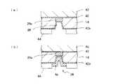
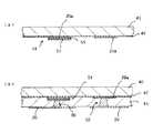
【従来の技術】
半導体装置に用いる半導体装置用多層基板には、図18に示す半導体装置用多層基板(以下、単に多層基板と称することがある)がある。図18に示す多層基板は、コア基板としての樹脂基板102を貫通するスルーホールヴィア110、110・・によって、樹脂基板102の両面に形成された上層部106a及び下層部106bの各々に形成された導体配線104、104・・等は電気的に接続されている。
また、上層部106a及び下層部106bの各層においても、樹脂製の絶縁層の両面に形成された導体配線104、104・・等の電気的な接続は、各絶縁層を貫通して形成されたヴィア118、118・・によってなされている。
更に、上層部106aの最上層には、搭載される半導体素子120の電極端子122、122・・と電気的に接続されるパッド124、124・・が形成されており、かかる最上層の上面は、パッド124、124・・を除きソルダレジスト126によって覆われている。
一方、下層部106bの最下層には、外部接続端子としてのはんだボール128、128・・が装着されるパッド130、130・・が形成されており、かかる最下層の下面は、パッド130、130・・を除きソルダレジスト132によって覆われている。
【0003】
図18に示す半導体装置用多層基板は、図19に示すビルドアップ法によって製造できる。かかるビルドアップ法によれば、図18に示す上層部116aと下層部116bとは同時に形成される。このため、図19では、上層部116aの形成工程を示し、下層部116bの形成工程を省略した。
図19に示す製造方法では、先ず、銅箔100が両面に形成された樹脂基板102に、ドリル等によってヴィア用のスルーホールを穿設した後、スルーホールに、その内壁面に無電解めっきによって形成した銅薄膜層を形成し、必要に応じて電解めっきによって所定厚さとするスルーホールめっきを施し、スルーホールヴィア110を形成する〔図19(a)の工程〕。
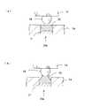
次いで、銅箔100にサブトラクティプ法によって導体配線104、104・・及びパッド105等を形成した後〔図19(b)の工程〕、樹脂基板102の導体配線形成面(樹脂基板102の両面)に、熱硬化樹脂であるポリイミド樹脂から成る樹脂フィルム106の片面に銅箔108が形成された片面金属箔フィルムを接着し〔図19(c)の工程〕、ヴィア形成箇所に導体配線104のランド部に達する凹部107、107・・をレーザ光によって形成する〔図19(d)の工程〕。形成された凹部107は、導体配線104の表面によって底面が形成された、開口面積が底面面積よりも大となる円錐台形状である。
尚、スルーホールヴィア110内にも、樹脂基板102と片面金属箔フィルムとを接着する際に、ポリイミド樹脂等が充填される。
【0004】
この凹部107の各内壁面には、銅箔108と電気的に接続される銅層112を形成する〔図19(e)の工程〕。かかる銅層112は、凹部107を除いて銅箔108をレジスト114によって覆っておき、凹部107の内壁面のみに無電解銅めっき又は銅スパッタ等によって形成した銅薄膜層を、必要に応じて電解めっきによって所定厚さとしたものである。
その後、レジスト114を除去し、銅箔108にサブトラクティブ法によって導体配線116等を形成する。この様にして形成された下層の導体配線114と上層の導体配線116とは、ヴィア118によって電気的に接続される。
かかる(c)〜(f)の工程を繰り返すことによって、図18に示す半導体装置用多層基板を得ることができる。
【0005】
【発明が解決しようとする課題】
図19に示すビルドアップ法によって得られた図18に示す多層基板によれば、集積度が進展した半導体素子120でも搭載可能である。
しかし、図18の多層基板の上層部106aでは、樹脂基板102から半導体素子120を搭載する最上層面(半導体素子120の搭載面)の方向に各層を順次形成するため、半導体素子120の搭載面の平坦性が低下し易い。このため、図18の多層基板の搭載面に、例えばフリップチップ方式で半導体素子120を搭載した際に、半導体素子120の電極端子122、122・・のうち、多層基板の最上層面に形成されたパッド124、124・・と当接しないものが発生するおそれがある。
また、図19に示すビルドアップ法においては、コア基板としての樹脂基板102の両面に同時に各層を積み上げる。樹脂基板102の片面のみに各層を形成すると、得られた多層基板が反ってしまうことがあるからである。このため、上層部106aのみで十分な場合であっても、得られる多層基板の反り防止として下層部106bを形成することを要し、得られた多層基板が厚くなる。
そこで、本発明の課題は、半導体素子が搭載される搭載面を可及的に平坦に形成でき、且つ厚さを可及的に薄く形成し得る半導体装置用多層基板及びその製造方法を提供することにある。
【0006】
【課題を解決するための手段】
本発明者等は、前記課題を解決すべく、検討した結果、半導体素子を搭載する半導体素子搭載面側から外部接続端子装着面の方向に順次導体配線及び絶縁層を形成することによって、コア基板を用いることなく多層基板を形成できること、及び多層基板の半導体素子搭載面を可及的に平坦にできることが判明し、本発明に到達した。
すなわち、本発明は、導体配線が絶縁層を介して多層に形成されて成る多層基板の一面側が、搭載される半導体素子の電極端子と接続されるように、半導体素子用パッドが露出する半導体素子搭載面であり、且つ前記多層基板の他面側が、外部接続端子用パッドが露出する外部接続端子装着面である半導体装置用多層基板において、該半導体素子用パッドと外部接続端子用パッドとが、前記絶縁層の各々に形成された導体配線及びパッドの少なくとも一方と各絶縁層を貫通するヴィアとによって電気的に接続されており、前記絶縁層の各々に形成された全てのヴィアが、前記絶縁層の外部接続端子装着面側に開口されていると共に、前記絶縁層の半導体素子搭載面側に形成された導体配線又はパッドの外部接続端子装着面側の内面によって底面が形成された、開口面積が底面面積よりも大となる円錐台状の凹部に形成されていることを特徴とする半導体装置用多層基板にある。
【0007】
また、本発明は、導体配線が絶縁層を介して多層に形成されて成る多層基板の一面側が、搭載される半導体素子の電極端子と接続されるように、半導体素子用パッドが露出する半導体素子搭載面であり、且つ前記多層基板の他面側が、外部接続端子用パッドが露出する外部接続端子装着面である半導体装置用多層基板を製造する際に、該半導体素子用パッドが形成される半導体素子搭載面側から前記外部接続端子用パッドが形成される外部接続端子装着面側に順次導体配線及び絶縁層を形成すると共に、前記導体配線及び絶縁層を順次形成する際に、前記絶縁層の半導体素子搭載面側に形成する導体配線及びパッドの少なくとも一方と、前記絶縁層の外部接続端子装着面側に形成する導体配線及びパッドの少なくとも一方とを、前記絶縁層を貫通して電気的に接続するヴィアを、前記絶縁層の外部接続端子装着面側に開口され、且つ前記絶縁層の半導体素子搭載面側に形成された導体配線及びパッドの少なくとも一方の外部端子接続装着面側の内面が底面に露出する、開口面積が底面面積よりも大の円錐台状の凹部に形成することを特徴とする半導体装置用多層基板の製造方法にある。
【0008】
かかる本発明において、半導体素子用パッドを覆う絶縁層を金属板の一面側に形成した後、前記絶縁層の表面に開口され、且つ前記半導体素子用パッドが底面に露出された、開口面積が底面面積よりも大の円錐台状の凹部にヴィアを形成すると共に、前記凹部の周縁部を形成する絶縁層の表面に所定の導体配線及びパッドの少なくとも一方を形成し、次いで、外部接続端子装着層を形成した後、前記金属板をエッチングして除去することによって半導体素子搭載用層を形成すること、或いは金属板の一面側に、前記金属板をエッチングするエッチング液によって実質的にエッチングされない金属から成る金属層を形成した後、前記金属層上に形成した半導体素子用パッドを覆う絶縁層の表面に開口され、且つ前記半導体素子用パッドが底面に露出された、開口面積が底面面積よりも大の円錐台状の凹部にヴィアを形成すると共に、前記凹部の周縁部を形成する絶縁層の表面に所定の導体配線及びパッドの少なくとも一方を形成し、次いで、外部接続端子装着層を形成した後、前記金属板及び金属層をエッチングして除去することによって半導体素子搭載用層を形成することによって、多層基板の製造工程において、金属板を補強板として使用でき基板の搬送等を容易に行うことができる。
【0009】
ここで、金属板の一面側に、前記金属板をエッチングするエッチング液によって実質的にエッチングされない樹脂から成る樹脂層を形成した後、前記金属板上に形成した半導体素子用パッドを覆う樹脂層の表面に開口され、且つ前記半導体素子用パッドが底面に露出された、開口面積が底面面積よりも大の円錐台状の凹部にヴィアを形成すると共に、前記凹部の周縁部を形成する樹脂層の表面に所定の導体配線及びパッドの少なくとも一方を形成し、次いで、外部接続端子装着層を形成した後、前記金属板をエッチングして除去することによって半導体素子搭載用層を形成することによって、半導体装置用多層基板の製造工程の省略を可能とすることができる。
【0010】
また、金属板をエッチングして除去する際に、半導体素子搭載面の周縁部に金属枠体が形成されるように、前記金属板をエッチングすることによって、得られた多層基板の強度を向上でき、搬送等を容易にすることができる。
かかる金属枠体は、得られた半導体装置用多層基板の周縁部に、別体に形成したものを接合してもよい。
更に、ヴィアを形成する際に、絶縁層に形成した円錐台状の凹部の内壁面に沿って凹状の金属層を電解めっきによって形成することによって、凹状のヴィアを容易に形成できる。
他方、ヴィアを形成する際に、絶縁層に形成した円錐台状の凹部に円錐台状のヴィアを電解めっきによって金属を充填して形成した後、前記円錐台状のヴィアの端面を含む絶縁層の開口面側を平坦面に研磨することによって、中実ヴィアを形成した絶縁層の凹部の開口面側を平坦面に形成できる。
【0011】
この様な本発明において、半導体素子用パッドを、少なくとも二層のめっき金属層によって形成し、その際に、搭載する半導体素子の電極端子と当接するめっき金属層を貴金属めっきによって形成することによって、下層のめっき金属層の酸化等を防止できる。
或いは半導体素子用パッドを、少なくとも二層のめっき金属層によって形成し、その際に、搭載する半導体素子の電極端子と当接するめっき金属層を、前記半導体素子の電極端子と半導体素子用パッドとを電気的に接続するリフロー工程において溶融する低融点金属によって形成することにより、半導体素子のフリップチップボンディングを容易とすることができる。
また、半導体素子用パッドを形成する際に、コンデンサを作り込むこともできる。
【0012】
従来のビルドアップ法による多層基板は、外部接続端子装着面を具備する外部接続端子装着層側から半導体素子搭載面を具備する半導体素子搭載層の方向に順次導体配線及び絶縁層を形成するため、最後に形成する半導体素子搭載層は、それまでに形成した層の凹凸が積層されて拡大し、半導体素子搭載面の平坦性が劣ることがある。
この点、本発明によれば、半導体素子搭載面を具備する半導体素子搭載層側から外部接続端子装着面を具備する外部接続端子装着層の方向に順次導電配線及び接続層を形成するため、半導体素子搭載層を最初に形成できる結果、半導体素子搭載面を可及的に平坦面とすることができる。
ところで、最後に形成する外部接続端子装着層は、それまでに形成した絶縁層等の凹凸の影響を受けているが、外部接続端子のサイズは半導体素子の電極端子よりも大きく、外部接続端子装着面の多少の凹凸は吸収可能である。このため、外部接続端子装着面の平坦性の要求は、半導体素子搭載面の平坦性の要求よりも緩和されており問題とならない。
【0013】
【発明の実施の形態】
本発明に係る半導体装置用多層基板の一例を図1に示す。図1は、半導体装置用多層基板の部分断面図である。この図1に示す半導体装置用多層基板10は、導体配線12、12・・がポリイミド樹脂やポリフェニレンエーテル等の樹脂から成る絶縁層14、14・・を介して多層に配されて成る多層基板(以下、多層基板10と称することがある)である。かかる多層基板10の一面側は、搭載する半導体素子16の電極端子18と接続されるように、半導体素子用パッド20a、20a・・が露出する半導体素子搭載面であり、多層基板10の他面側は、外部接続端子としてのはんだボール22、22・・を装着する外部接続端子用パッド24、24・・が露出する外部接続端子装着面である。
この多層基板10の半導体素子搭載面及び外部接続端子装着面には、半導体素子用パッド20a及び外部接続端子用パッド24を除き、ソルダレジスト26、26によって覆われている。
【0014】
この様な多層基板10において、半導体素子用パッド20aと外部接続端子用パッド24とは、図1に示す様に、絶縁層14、14・・の各層に形成された導体配線12及びパッド20の少なくとも一方と、絶縁層14を貫通して形成されたヴィア28とによって電気的に接続されている。かかるヴィア28は、絶縁層14の外部接続端子装着面側に開口されていると共に、半導体素子搭載面側に形成された導体配線12又はパッド20の面によって底面が形成された凹部30内に形成されている。
この凹部30は、開口面積が底面面積よりも大の円錐台状である。図1に示すヴィア28は、円錐台状の凹部30の内壁面に沿って金属層が所定厚さに形成されて成る凹状ヴィアである。
【0015】
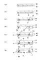
図1に示す多層基板10は、図2〜図5に示す製造方法によって、半導体素子搭載面が形成された半導体素子搭載層から外部接続端子装着面が形成された外部接続端子装着層の方向に順次導線配線及び絶縁層を形成して製造できる。
先ず、金属板としての銅板40の一面側にシードレイヤ42を形成する〔図2(a)〕。このシードレイヤ42を形成する銅板40の面の平均粗さ(Ra)は0.1μm以下であることが好ましい。シードレイヤ42の形成面の平均粗さ(Ra)が0.1μmを越える場合、平均粗さ(Ra)が0.1μm以下となるように、銅板40のシードレイヤ42の形成面に研磨を施すことが好ましい。
かかる銅板40の一面側に形成されたシードレイヤ42は、その拡大図に示す様に、銅板40の面に直接接触する厚さ0.01μmのクロム(Cr)層41aと、クロム(Cr)層41a上に形成した厚さ0.1μmの銅(Cu)層41bとから成る。かかるクロム(Cr)層41aは、後述する様に、銅板40をエッチングする際に、銅板40をエッチングするエッチング液によってエッチングされない金属から成る金属層である。また、銅(Cu)層41bは、後述する電解めっきの際の給電層である。これらクロム(Cr)層41a及び銅(Cu)層41bは、スパッタ、蒸着、或いは無電解めっきによって形成できる。
尚、クロム(Cr)層41aに代えて、銅板40をエッチングするエッチング液によってエッチングされるものの、エッチング速度が著しく遅い金属層を形成してもよい。
【0016】
銅板40の一面側に形成したシードレイヤ42上には、半導体素子16の電極端子18が接続される銅から成る、厚さ10μm程度の半導体素子用パッド20a、20a・・を形成する〔図2(b)〕。この半導体素子用パッド20aは、シードレイヤ42上に形成したフォトレジスト層にパターニングを施し、半導体素子用パッド20a等を形成する部分のシードレイヤ42を露出させた後、シードレイヤ42、特に銅層41(b)を給電層とする電解めっきによって形成できる。
半導体素子用パッド20a、20a・・を形成した銅板40の面には、厚さ10μm程度の半導体素子用パッド20a、20a・・を覆うように、熱硬化性樹脂であるポリイミド樹脂を印刷等によって塗布し硬化して絶縁層14を形成する〔図2(c)〕。この絶縁層14に、YAGレーザや炭酸ガスレーザ等のレーザ光によってヴィア形成用の凹部30を形成する。形成した凹部30は、絶縁層14の表面に開口されていると共に、半導体素子用パッド20aの面によって底面が形成された凹部であって、開口面積が底面面積よりも大の円錐台状である〔図2(d)〕。
ここで、凹部30をYAGレーザ等のレーザ光によって形成しているが、エッチングでも形成できる。
尚、凹部30は、絶縁層14を感光性樹脂によって形成してフォトリソ法によって形成してもよい。
【0017】
形成された凹部30の内壁面を含む絶縁層14の全表面に、シードレイヤ42aを形成する〔図2(e)〕。このシードレイヤ42aも、凹部30の内壁面を形成する絶縁層14の面に直接接触する厚さ0.01μmのクロム(Cr)層41aと、クロム(Cr)層41a上に形成した厚さ0.1μmの銅(Cu)層41bとから成る。かかるクロム(Cr)層41a及び銅(Cu)層41bはスパッタによって形成できる。
更に、図3(a)に示す様に、シードレイヤ42a上に形成したフォトレジスト層44にパターニングを施し、ヴィアや導体配線を形成する部分のシードレイヤ42aを露出する。
次いで、シードレイヤ42aを給電層とする電解めっきによって、シードレイヤ42aが露出する部分に所定厚さの銅層46を形成してヴィア28や厚さ10μm程度の導体配線を形成する。このヴィア28は、凹部30の内壁面に沿って所定厚さの銅層46が形成された凹状ヴィアである。
その後、フォトレジスト層44を除去し、ヴィア28と導体配線との間等のシードレイヤ42aをエッチングして除去することによって、図2(f)に示す様に、絶縁層14の表面にヴィア28、28・・及び導体配線12、12・・を形成できる。
尚、図2(a)や図2(e)に示すシードレイヤ42aを構成するクロム(Cr)層41aは、クロム(Cr)層41aに代えてチタン(Ti)層をスパッタによって形成してもよく、シードレイヤ42aに代えて無電解めっきによって薄膜状の銅層を形成してもよい。
【0018】
更に、図2(c)〜(f)及び図3の工程を繰り返すことによって、半導体素子搭載面を具備する半導体素子搭載層側から外部接続端子装着面を具備する外部接続端子装着層の方向に順次導体配線及び絶縁層を形成し、図4に示す多層基板10の中間体10aを得ることができる。得られた中間体10aの一面側には、半導体素子用パッド20a、20a・・が形成された半導体素子搭載面に、シードレイヤ42を介して銅板40が接合され、中間体10aの他面側には、外部接続端子用パッド24、24・・が形成されている。かかる銅板40は、中間体10a等の補強板としての役割を奏し、中間体10a等の搬送等の取扱を容易にできる。
唯、最終的に図1に示す多層基板10を得るためには、中間体10aの銅板40をエッチングによって除去することが必要である。この銅板40のエッチングは、銅板40を形成する銅をエッチングするエッチング液によって行うが、銅板40のエッチングの完了時期を厳格に管理することは困難である。このため、シードレイヤ42に、銅板40のエッチング液にエッチングされないクロム(Cr)層41a〔図2(a)〕を形成しておくことによって、銅板40のエッチングが完了した際に、半導体素子用パッド20a等が更にエッチングされることを防止できる。
【0019】
つまり、図5(a)に示す銅版40のエッチングは、銅板40の全面を一様な速度でエッチングすることは至難のことであり、エッチング面に凹凸が形成され易い。この点、シードレイヤ42に銅板40のエッチング液にエッチングされないクロム(Cr)層41aを形成しておくことによって、銅板40のエッチングが速く進行する個所においても、エッチングがシードレイヤー42のクロム(Cr)層41aに到達したとき、エッチングがストップする。このため、銅版40のエッチングがストップする個所が経時と共に順次拡大し、図5(b)に示す様に、シードレイヤー42のクロム(Cr)層41aの全面が露出した時点で銅板40のエッチングが終了する。
次いで、シードレイヤー42をエッチングによって除去することによって、図5(c)に示す様に、半導体素子用パッド20aの表面が露出する。かかるシードレイヤー42をエッチングによって除去する際には、先ず、クロム(Cr)層41aを、クロム(Cr)をエッチングするが銅(Cu)をエッチングしないエッチング液によってエッチングし、その後、銅(Cu)層41bもエッチングによって除去する。
尚、シードレイヤ42の銅層41bをエッチングする場合は、同時に銅製の半導体素子用パッド20aも同時にエッチングがなされるが、銅層41bの厚さは0.1μm程度であり、半導体素子用パッド20aの厚さは10μm程度であるため問題とはならない。
【0020】
この様に、図5に示す様に、図4に示す多層基板10aの銅板40及びシードレイヤ42を除去した後、半導体素子用パッド20a及び外部接続端子用パッド24を除き半導体素子搭載面及び外部接続端子装着面に、ソルダレジスト26、26を塗布することによって、図1に示す多層基板10を得ることができる。
銅板40及びシードレイヤ42を除去した、半導体素子用パッド20aの表面を含む絶縁層14の表面を極めて平坦面に形成でき、半導体素子16の電極端子18と半導体素子用パッド20aとを確実に当接させることができる。
ところで、図3に示す工程において、凹部30の内壁面を含む絶縁層14の表面に形成したシードレイヤ42a上にフォトレジスト層44を形成した後、フォトレジスト層44にパターニングを施し、ヴィアや導体配線を形成する部分のシードレイヤ42aを露出させているが、形成するヴィアが小径になるにしたがって凹部30の内径も小径となり、凹部30の底面に充分な光量が届き難くなる。このため、凹部30内に充填されたフォトレジスト、特に凹部30の底面近傍のフォトレジストが充分に感光され難くなり、凹部30内のフォトレジストを完全に除去することが困難となる傾向にある。
このため、図6(a)に示す様に、シードレイヤ42aを給電層とする電解めっきによって、シードレイヤ42a上に銅層47を形成して凹部30を浅くし、凹部30の底面に充分な光量が届くようにした後、凹部30にフォトレジストを充填してフォトレジスト層44をシードレイヤ42a上に形成する。
【0021】
次いで、図6(b)に示す様に、フォトレジスト層44にパターニングを施し、ヴィアや導体配線を形成する部分の銅層47を露出させる。このパターニングの際に、凹部30に充填されたフォトレジストは充分に感光されるため、完全に除去できる。
その後、シードレイヤ42a及び銅層47を給電層としての電解めっきを施し、所定厚さの銅層46から成る導体配線及び凹部30の内壁面に沿って形成された所定厚さの銅層46から成る凹状のヴィア28の少なくとも一方を形成する。
更に、ヴィア28や導体配線の間に形成されたシードレイヤ42a及び銅層47をエッチングして除去することによって、図2(f)に示す様に、絶縁層14の表面にヴィア28、28・・及び導体配線12、12・・を形成できる。
尚、図2〜図6において、クロム(Cr)層41aと銅(Cu)層41bとから成るシードレイヤ42aを形成しているが、クロム(Cr)層41aに代えてチタン(Ti)層をスパッタによって形成してもよく、銅板40に代えてアルミ板又はステンレス板を用いてもよい。
【0022】
ここで、図6に示す方法によって形成したヴィアよりも更に小径のヴィアを形成する場合には、図7に示す方法を採用することが好ましい。先ず、図7(a)に示す様に、薄膜状銅層54をスパッタ又は無電解めっき等によって形成し、この薄膜状銅層54を給電層として電解めっきによって、薄膜状銅層54上に凹部30を銅によって充填し得る厚さの銅層56を形成する〔図7(b)〕。かかる銅層56の上面には、凹部30に対応する位置に小凹部55が形成されるが、形成するヴィアが小径となるにしたがって凹部30も小径となり、銅層56の上面に形成される小凹部55も微小となるため、銅銅56の上面は実質的に平坦面に形成される。
次いで、図7(c)に示す様に、銅層56にパターニングを施し、ヴィア28及び導体配線12を形成する。
尚、薄膜状銅層54は、シードレイヤ42を形成するクロム(Cr)層41a又はチタン(Ti)層を形成した後、スパッタ又は無電解めっき等によって形成してもよい。
【0023】
図1〜図7において、半導体素子用パッド20aは銅層のみによって形成されているが、互いに異なる種類の金属から成る少なくとも二層の金属層によって形成されていてもよい。図8には、半導体素子用パッド20aが、銅層21と金層23によって形成されている例を示す。この金層23は、半導体素子用パッド20aの表層を形成し、銅層21の酸化防止等の保護層としての役割を奏する。かかる金層23も、金(Au)−パラジウム(Pd)ーニッケル(Ni)或いは金(Au)ーニッケル(Ni)の複合構造であってもよい。
かかる図8に示す半導体素子用パッド20aを形成するには、図9(a)に示す様に、図2(a)に示すシードレイヤ42の表面に形成した樹脂層43の所定の個所に、レーザ或いはエッチングによって半導体素子用パッド20a形成用の凹部45を形成する。
この凹部45には、シードレイヤ42を給電層として電解金めっきによって、シードレイヤ42に接触する金層23を形成した後、電解銅めっきによって銅層21を形成する[図9(b)]。
更に、樹脂層43を除去することによって、二層構造の半導体素子用パッド20aを形成できる[図9(c)]。
尚、その後は、図2(c)以降と同様な工程で多層基板を得ることができる。
【0024】
ここで、図8に示す半導体素子用パッド20aの金層23を、図10(a)に示す様に、はんだ層25としてもよい。はんだ層25を形成するはんだは、リフロー工程の加熱雰囲気下で溶融する低融点金属であって、溶融はんだは、搭載された半導体素子の電極端子と半導体素子用パッド20aとを電気的に接続することができる。このはんだ層25を形成するはんだとしては、リフロー工程の加熱雰囲気下で溶融するものであればよいが、錫(Sn)−銀(Ag)等の鉛(Pb)フリーの合金が好ましい。
この様に、半導体素子用パッド20aの表層にはんだ層25を形成しておくことによって、図10(a)に示す様に、搭載された半導体素子16の電極端子18のうち、半導体素子用パッド20aの表面に当接しない電極端子18が存在しても、リフロー工程を通過した半導体素子16の電極端子18と半導体素子用パッド20aとは、図10(b)に示す様に、はんだ層25によって電気的に接続され、最終的に得られた半導体装置の信頼性を向上できる。つまり、リフロー工程の加熱雰囲気下ではんだ層25が溶融して溶融はんだとなったとき、溶融はんだは表面張力で楕円球状となって、絶縁層14の表面から楕円球状の溶融はんだの一部が突出して電極端子18と接触するためである。
尚、図10(a)に示す半導体素子用パッド20aは、図9に示す工程において、金層23を形成する電解金めっきに代えて、電解はんだめっきによってはんだ層25を形成する他は、図9に示す工程と同様にして形成できる。
【0025】
これまで説明してきた図1〜図10では、銅板40の一面側にシードレイヤ42を形成してきたが、図8に示す様に、半導体素子用パッド20aの表層を金層23によって形成されている場合には、銅板40をエッチングするエッチング液によって金層23はエッチングされないため、シードレイヤ42の形成を不要にできる。
一方、図10(a)に示す様に、半導体素子用パッド20aの表層をはんだ層25によって形成されている場合には、銅板40をエッチングするエッチング液によってはんだ層25もエッチングされるが、そのエッチング速度が銅板40のエッチング速度よりも著しく遅く、実質的にはんだ層25はエッチングされないため、この場合も、シードレイヤ42の形成を不要にできる。
また、半導体素子用パッド20aを銅層のみで形成する場合でも、多層基板の製造工程の短縮を図るべく、図11に示す様に、シードレイヤ42を省略して多層基板を形成することができる。
図11に示す製造方法では、先ず、金属板としての銅板40の一面側に樹脂層43を形成する〔図11(a)〕。この銅板40の樹脂層43を形成する面は、図2に示す製造方法と同様に、平均粗さ(Ra)は0.1μm以下であることが好ましい。樹脂43の形成面の平均粗さ(Ra)が0.1μmを越える場合、平均粗さ(Ra)が0.1μm以下となるように、銅板40の樹脂層43の形成面に研磨を施すことが好ましい。
この樹脂層43は、銅板40をエッチングするエッチング液にエッチングされない樹脂又は実質的にエッチングされないエポキシ、ポリイミド、ポリフェニレンエーテル等の樹脂によって形成されている。
【0026】
銅板40の一面側に形成した樹脂層43の所定個所には、図11(b)に示す様に、レーザ或いはエッチングによって半導体素子用パッド20a形成用の凹部45を形成する。
この凹部45には、銅板40を給電層として電解金めっきによって、銅板40に接触する金層23を形成した後、電解銅めっきによって銅層21を形成するすることによって、二層構造の半導体素子用パッド20aを形成できる[図11(c)]。
次いで、樹脂層43の上面に、半導体素子用パッド20aを覆うように樹脂層を積層する。この樹脂層43の上面に積層する樹脂は、図11(d)に示す様に、樹脂層43を形成する樹脂と同一樹脂を用い、樹脂層43と一体化された絶縁層45を形成する。
かかる絶縁層45には、YAGレーザや炭酸ガスレーザ等のレーザ光によってヴィア形成用の凹部30を形成する。形成した凹部30は、絶縁層45の表面に開口されていると共に、半導体素子用パッド20aの面によって底面が形成された凹部であって、開口面積が底面面積よりも大の円錐台状である〔図11(e)〕。
ここで、凹部30をYAGレーザ等のレーザ光によって形成しているが、エッチングでも形成できる。
尚、凹部30は、絶縁層45を感光性樹脂によって形成してフォトリソ法によって形成してもよい。
【0027】
形成された凹部30の内壁面を含む絶縁層45の全表面に、無電解銅めっき、スパッタ、或いは蒸着によって薄膜状銅層43aを形成する〔図11(f)〕。この薄膜状銅層43aの厚さは30の内壁面を形成する絶縁層45の面に直接接触する厚さは0.1μm程度である。
更に、図3(a)に示す様に、薄膜状銅層43a上に形成したフォトレジスト層44にパターニングを施し、ヴィアや導体配線を形成する部分の薄膜状銅層43aを露出する。
次いで、薄膜状銅層43aを給電層とする電解めっきによって、薄膜状銅層43aが露出する部分に所定厚さの銅層46を形成してヴィア28や厚さ10μm程度の導体配線を形成する。このヴィア28は、凹部30の内壁面に沿って所定厚さの銅層46が形成された凹状ヴィアである。
その後、フォトレジスト層44を除去し、ヴィア28と導体配線との間等のシードレイヤ42aをエッチングして除去することによって、図11(g)に示す様に、絶縁層45の表面にヴィア28、28・・及び導体配線12、12・・を形成できる。
【0028】
図1〜図11に示す多層基板10のヴィア28は、円錐台状の凹部30の内壁面に沿って金属層が所定厚さに形成されて成る凹状であるため、多層基板10の外部接続端子装着面の多少の凹凸が形成され易い。かかる凹凸は、外部接続端子用パッド24、24・・に装着される、外部接続端子としてのはんだボール22、22・・が、半導体素子16の電極端子18よりも大きいため、ある程度は吸収可能である。しかし、はんだボール22の小粒化が進展すると、外部接続端子装着面も平坦性が要求される。
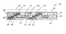
この様に、外部接続端子装着面の平坦性が要求される多層基板としては、図12に示す多層基板50が好ましい。図12に示す多層基板50では、図1の多層基板10と共通する構成部材は同一番号を付けて詳細な説明を省略した。
【0029】
図12に示す多層基板50において、ヴィア52は、円錐台状の凹部30内に銅が充填されて成る円錐台状の中実体であり、ヴィア52の端面を含む絶縁層14の凹部30の開口面側に研磨が施されている点が、図1の多層基板10と相違する点である。この様に、ヴィア52の端面を含む絶縁層14の凹部30の開口面側に研磨を施すことによって、多層基板50の外部接続端子装着面を、図1に示す多層基板10の外部接続端子装着面よりも平坦面に形成できる。このため、外部接続端子用パッド24、24・・に装着するはんだボール22、22・・の小粒化を更に図ることができる。
図12に示す多層基板50は図13及び図14に示す製造方法によって形成できる。図13に示す製造方法においても、図2(a)〜(d)に示す工程を採用し、YAGレーザ等のレーザ光を用いて絶縁層14にヴィア形成用の凹部30を形成する〔図2(d)〕。この凹部30は、絶縁層14の外部接続端子装着面側に開口されていると共に、半導体素子用パッド20aの面によって底面が形成された、開口面積が底面面積よりも大となる円錐台状である。
【0030】
かかる凹部30の内壁面を含むて絶縁層14の表面には、図13(a)に示す様に、薄膜状銅層54をスパッタ等によって形成し、この薄膜状銅層54を給電層として電解めっきによって、凹部30を銅によって充填し得る厚さの銅層56を薄膜状銅層54上に形成する〔図13(b)〕。かかる銅層56の上面には、凹部30に対応する位置に、小凹部55が形成される。
このため、絶縁層14の凹部30の開口面側に研磨を施する。この研磨によって、銅層56を除去すると共に、凹部30に銅が充填されて形成されたヴィア52の端面も研磨されるため、凹部30の開口面側である絶縁層14の表面は平坦面に形成できる〔図13(c)〕。
次いで、研磨を施した絶縁層14の研磨面に電解めっき、無電解めっき、或いはスパッタ等によって所定厚さに形成した銅層に、フォトリソ法等によってパッド20及び導体配線12を形成した後〔図13(d)〕、図13(a)〜(d)の工程を繰り返すことによって、半導体素子搭載面を具備する半導体素子搭載層から外部接続端子装着面を具備する外部接続端子装着層の方向に順次各層を形成し、図14に示す中間体50aを得ることができる。
【0031】
得られた中間体50aには、図4に示す多層基板10aと同様に、半導体素子搭載面に、シードレイヤ42を介して銅板40が接合されている。この銅板40は、中間体50a等の補強板の役割を奏し、中間体50a等の搬送等の取扱を容易とすることができる。
かかる中間体50aの銅板40をエッチングして除去する際には、銅をエッチングするエッチング液によって銅板40をエッチングし、シードレイヤ42を形成するクロム(Cr)層41〔図2(a)〕に銅板40のエッチングが到達したとき、銅板40のエッチングを終了する。
更に、クロム(Cr)層41も、銅板40のエッチングが完了した後、クロム(Cr)をエッチングするが銅(Cu)をエッチングしないエッチング液によってエッチングし、その後、シードレイヤ42を形成する銅層41bもエッチングによって除去される。
この様に、図14に示す多層基板50aの銅板40及びシードレイヤ42を除去した後、半導体素子用パッド20a及び外部接続端子用パッド24を除き半導体素子搭載面及び外部接続端子装着面に、ソルダレジスト26、26を塗布することによって、図12に示す多層基板50を得ることができる。
【0032】
以上、説明してきた図1〜図14に示す多層基板では、銅板40を完全に除去しているが、図15に示す様に、銅板40の多層基板10の周縁に沿う部分を残留することによって枠体41が形成される。この枠体41は、多層基板10の補強材として作用し、多層基板10の搬送等の取扱等の取扱性を向上できる。
また、金属製の枠体41が、シードレイヤ42を介して多層基板10に設けられているため、枠体41とシードレイヤ42との間に、薄膜状の高誘電体皮膜を形成することによって薄膜コンデンサを形成することも可能であり、図16に示す様に、多層基板50に薄膜コンデンサ51を作り込むことも可能である。図16は、図12に示す多層基板50であり、搭載する半導体素子16の電極端子18の直近に薄膜コンデンサ51を形成した例である。この薄膜コンデンサ51は、図17(a)に示す様に、銅板40の一面側に形成されたシードレイヤ42に形成する。先ず、シードレイヤ42の表面にスパッタで形成した半導体素子用パッド20aの表面に、チタン酸ストロンチウム(SrTiO3)やチタン酸バリウム(BaTiO3)等の高誘電体材料から成る高誘電体層53をスパッタによって形成した後、この高誘電体層53の表面にスパッタで薄膜銅層57を形成することにより、薄膜コンデンサ51を形成できる。
次いで、薄膜コンデンサ51及び半導体素子用パッド20aが形成された銅板40には、図13(a)〜(d)の工程を繰り返すことによって図17(b)に示すヴィア52等を形成できる。
【0033】
更に、図2〜図9、図11、図13〜図15、図17には、銅板40を用いていたが、銅板40に代えてアルミニウム製の金属板又はステンレス製の金属板を使用できる。この様に、アルミニウム製又はステンレス製の金属板を用いる場合にも、半導体素子用パッド20a等と金属板との密着性等を向上すべく金属板と半導体素子用パッド20a等との間にシールドレイヤ42を形成してもよい。
ここで、半導体素子用パッド20a等を銅製とし、金属板をアルミニウム製とした場合、エッチング液を選択することによって、銅から成る半導体素子用パッド20aをエッチングすることなく金属板をエッチングでき、シードレイヤ42を不要とすることができる。
尚、多層基板10の搬送等の取扱性等を更に一層向上せんとする場合には、図1に示す様に、多層基板10の周縁部に所定の強度を有する金属製の枠体17を別体に形成して接合してもよい。
【0034】
【発明の効果】
本発明によれば、多層基板の半導体素子搭載面を可及的に平坦面とすることができ、搭載する半導体素子の電極端子と多層基板の半導体素子用パッドとを確実に接続することができる。
また、コア基板を不要とすることができ、更に薄い多層基板を形成できる。
【図面の簡単な説明】
【図1】 本発明に係る半導体装置用多層基板の一例を示す部分断面図である。
【図2】 図1に示す半導体装置用多層基板の製造工程を示す工程図である。
【図3】 図1に示す半導体装置用多層基板の製造工程の一部について説明する説明図である。
【図4】 図1に示す半導体装置用多層基板の中間体を示す部分断面図である。
【図5】 図3に示す半導体装置用多層基板の製造工程の次の工程を説明するための工程図である。
【図6】 図3に示す半導体装置用多層基板の製造工程の一部についての他の方法を説明する説明図である。
【図7】 図3に示す半導体装置用多層基板の製造工程の一部についての他の方法を説明する説明図である。
【図8】 図1に示す半導体装置用多層基板の他の例を示す部分断面図である。
【図9】 図8に示す半導体装置用多層基板の製造方法を説明するための部分工程図である。
【図10】 図1に示す半導体装置用多層基板の他の例を示す部分断面図である。
【図11】 図2に示す半導体装置用多層基板の製造方法の他の例を説明するための工程図である。
【図12】 本発明に係る半導体装置用多層基板の他の例を示す部分断面図である。
【図13】 図12に示す半導体装置用多層基板の製造工程を示す工程図である。
【図14】 図12に示す半導体装置用多層基板の中間体を示す部分断面図である。
【図15】 本発明に係る半導体装置用多層基板の他の例を示す部分断面図である。
【図16】 薄膜コンデンサを作り込んだ半導体装置用多層基板の一例を説明する部分断面図である。
【図17】 図16に示す半導体装置用多層基板の製造方法を説明する工程図である。
【図18】 従来の半導体装置用多層基板を示す部分断面図である。
【図19】 図18に示す従来の半導体装置用多層基板の製造工程を示す工程図である。
【符号の説明】
10、50 半導体装置用基板
10a、50a 中間体
12 導体配線
14 絶縁層
16 半導体素子
18 電極端子
20 パッド
20a 半導体素子用パッド
22 外部接続端子
24 外部接続端子用パッド
26 ソルダレジスト
28、52 ヴィア
30 凹部
40 金属板(銅板)
41a クロム(Cr)層
41b 銅(Cu)層
42、42a シードレイヤ
44 フォトレジスト層
46、47 銅層[0001]
BACKGROUND OF THE INVENTION
The present invention relates to a multilayer substrate for a semiconductor device and a method for manufacturing the same, and more specifically, one side of a multilayer substrate in which conductor wiring is formed in a multilayer via an insulating layer is connected to an electrode terminal of a semiconductor element to be mounted. The present invention relates to a semiconductor device multilayer substrate on which a semiconductor element pad is formed and the other surface side of the multilayer substrate is an external connection terminal mounting surface on which external connection terminal pads are formed, and a method for manufacturing the same. .
[0002]
[Prior art]
As a multilayer substrate for a semiconductor device used for a semiconductor device, there is a multilayer substrate for a semiconductor device shown in FIG. 18 (hereinafter sometimes simply referred to as a multilayer substrate). The multilayer substrate shown in FIG. 18 is formed on each of the
Also, in each of the
Further,
On the other hand,
[0003]
The multilayer substrate for a semiconductor device shown in FIG. 18 can be manufactured by the build-up method shown in FIG. According to the build-up method, the upper layer portion 116a and the lower layer portion 116b shown in FIG. 18 are formed at the same time. For this reason, in FIG. 19, the formation process of the upper layer part 116a was shown, and the formation process of the lower layer part 116b was abbreviate | omitted.
In the manufacturing method shown in FIG. 19, first, a through hole for a via is drilled by a drill or the like in a
Next, after forming
The through hole via 110 is also filled with polyimide resin or the like when the
[0004]
A
Thereafter, the
By repeating these steps (c) to (f), the multilayer substrate for a semiconductor device shown in FIG. 18 can be obtained.
[0005]
[Problems to be solved by the invention]
According to the multilayer substrate shown in FIG. 18 obtained by the build-up method shown in FIG. 19, it is possible to mount even the
However, in the
In the build-up method shown in FIG. 19, the layers are stacked simultaneously on both surfaces of the
Accordingly, an object of the present invention is to provide a multilayer substrate for a semiconductor device that can form a mounting surface on which a semiconductor element is mounted as flat as possible and can be formed as thin as possible, and a method for manufacturing the same. There is.
[0006]
[Means for Solving the Problems]
As a result of studies to solve the above problems, the present inventors have formed a core substrate by sequentially forming a conductor wiring and an insulating layer in the direction from the semiconductor element mounting surface side where the semiconductor element is mounted to the external connection terminal mounting surface side. It has been found that a multilayer substrate can be formed without using and that the semiconductor element mounting surface of the multilayer substrate can be made as flat as possible.
That is, according to the present invention, a semiconductor element in which a pad for a semiconductor element is exposed so that one surface side of a multilayer substrate in which conductor wiring is formed in multiple layers via an insulating layer is connected to an electrode terminal of the mounted semiconductor element. In the multilayer substrate for a semiconductor device which is a mounting surface and the other surface side of the multilayer substrate is an external connection terminal mounting surface from which the external connection terminal pad is exposed, the semiconductor element pad and the external connection terminal pad are: Formed on each of the insulating layersAt least one of conductor wiring and pads And vias penetrating each insulating layer, all the vias formed in each of the insulating layers are opened to the external connection terminal mounting surface side of the insulating layer, and The bottom surface is formed by the inner surface of the insulating layer on the semiconductor element mounting surface side of the conductor wiring or pad on the external connection terminal mounting surface side, and is formed in a truncated cone-shaped recess whose opening area is larger than the bottom surface area. A multilayer substrate for a semiconductor device is provided.
[0007]
The present invention also provides a semiconductor element in which a pad for a semiconductor element is exposed so that one surface side of a multilayer substrate in which conductor wiring is formed in multiple layers via an insulating layer is connected to an electrode terminal of the mounted semiconductor element. A semiconductor device on which the semiconductor element pad is formed when manufacturing the multilayer substrate for a semiconductor device, which is a mounting surface and the other surface side of the multilayer substrate is an external connection terminal mounting surface from which the external connection terminal pad is exposed. The conductor wiring and the insulating layer are sequentially formed from the element mounting surface side to the external connection terminal mounting surface side on which the external connection terminal pad is formed, and when the conductor wiring and the insulating layer are sequentially formed, Form on the semiconductor element mounting surface sideAt least one of conductor wiring and pads And on the external connection terminal mounting surface side of the insulating layerAt least one of conductor wiring and pads Vias that are electrically connected through the insulating layer are opened on the external connection terminal mounting surface side of the insulating layer and formed on the semiconductor element mounting surface side of the insulating layer.At least one of conductor wiring and pads In the method of manufacturing a multilayer substrate for a semiconductor device, the inner surface of the external terminal connection mounting surface side is exposed to the bottom surface, and the opening area is formed in a truncated cone-shaped concave portion larger than the bottom surface area.
[0008]
In the present invention, an insulating layer covering the semiconductor element pad is formed on the one surface side of the metal plate, and then opened on the surface of the insulating layer, and the semiconductor element pad is exposed on the bottom surface. A via is formed in the conical recess having a larger area than the area, and a predetermined surface is formed on the surface of the insulating layer forming the peripheral edge of the recess.At least one of conductor wiring and pads Then, after forming the external connection terminal mounting layer, the metal plate is etched and removed to form a semiconductor element mounting layer, or the metal plate is etched on one side of the metal plate After forming a metal layer made of a metal that is not substantially etched by the etching solution, an opening is formed in the surface of the insulating layer covering the semiconductor element pad formed on the metal layer, and the semiconductor element pad is exposed to the bottom surface The via is formed in the truncated conical recess having an opening area larger than the bottom area, and a predetermined surface is formed on the surface of the insulating layer forming the peripheral edge of the recess.At least one of conductor wiring and pads Then, after forming the external connection terminal mounting layer, the metal plate and the metal layer are etched and removed to form a semiconductor element mounting layer. Can be used as a reinforcing plate, and the substrate can be easily transported.
[0009]
Here, a resin layer made of a resin that is not substantially etched by an etchant that etches the metal plate is formed on one side of the metal plate, and then the resin layer that covers the semiconductor element pad formed on the metal plate is formed. A resin layer forming a via in a truncated cone-shaped recess having an opening on the surface and the semiconductor element pad exposed on the bottom surface, the opening area being larger than the bottom surface area, and forming a peripheral portion of the recess Predetermined on the surfaceAt least one of conductor wiring and pads Then, after forming the external connection terminal mounting layer, it is possible to omit the manufacturing process of the semiconductor device multilayer substrate by forming the semiconductor element mounting layer by etching and removing the metal plate It can be.
[0010]
In addition, when the metal plate is removed by etching, the strength of the obtained multilayer substrate can be improved by etching the metal plate so that a metal frame is formed on the peripheral portion of the semiconductor element mounting surface. , Transportation and the like can be facilitated.
Such a metal frame may be bonded separately to the periphery of the obtained multilayer substrate for a semiconductor device.
Furthermore, when forming the via, the concave via can be easily formed by forming a concave metal layer along the inner wall surface of the truncated cone-shaped concave formed in the insulating layer by electrolytic plating.
On the other hand, when forming the via, after forming the truncated cone-shaped via by filling the truncated cone-shaped recess formed in the insulating layer with metal by electrolytic plating, the insulating layer including the end surface of the truncated cone-shaped via The opening side of thePolish Thus, the opening surface side of the recess of the insulating layer in which the solid via is formed can be formed on a flat surface.
[0011]
In the present invention, the semiconductor element pad is formed by at least two plated metal layers, and at that time, by forming a plated metal layer in contact with the electrode terminal of the semiconductor element to be mounted by noble metal plating, Oxidation of the lower plating metal layer can be prevented.
Alternatively, the semiconductor element pad is formed of at least two plated metal layers, and at this time, the plated metal layer contacting the electrode terminal of the semiconductor element to be mounted is formed by connecting the electrode terminal of the semiconductor element and the semiconductor element pad. By forming with a low melting point metal that melts in the reflow process for electrical connection, flip chip bonding of the semiconductor element can be facilitated.
In addition, a capacitor can be formed when forming the semiconductor element pad.
[0012]
In order to form a conductive wiring and an insulating layer sequentially in the direction from the external connection terminal mounting layer side having the external connection terminal mounting surface to the semiconductor element mounting layer having the semiconductor element mounting surface, the multilayer substrate by the conventional build-up method, The semiconductor element mounting layer to be formed last may be enlarged by stacking the unevenness of the layers formed so far, resulting in poor flatness of the semiconductor element mounting surface.
In this regard, according to the present invention, the conductive wiring and the connection layer are sequentially formed in the direction from the semiconductor element mounting layer side having the semiconductor element mounting surface to the external connection terminal mounting layer having the external connection terminal mounting surface. As a result of forming the element mounting layer first, the semiconductor element mounting surface can be made as flat as possible.
By the way, the external connection terminal mounting layer to be finally formed is affected by the unevenness of the insulating layer formed so far, but the size of the external connection terminal is larger than the electrode terminal of the semiconductor element, and the external connection terminal mounting Some irregularities on the surface can be absorbed. For this reason, the flatness requirement of the external connection terminal mounting surface is more relaxed than the flatness requirement of the semiconductor element mounting surface and does not cause a problem.
[0013]
DETAILED DESCRIPTION OF THE INVENTION
An example of a multilayer substrate for a semiconductor device according to the present invention is shown in FIG. FIG. 1 is a partial cross-sectional view of a multilayer substrate for a semiconductor device. 1 includes a
The semiconductor element mounting surface and the external connection terminal mounting surface of the
[0014]
In such a
The
[0015]
The
First, the
As shown in the enlarged view, the
Instead of the chromium (Cr)
[0016]
On the
The surface of the
Here, the
In addition, the recessed
[0017]
A
Further, as shown in FIG. 3A, the
Next, a
Thereafter, the
Note that the chromium (Cr)
[0018]
Further, by repeating the steps of FIGS. 2C to 2F and FIG. 3, the semiconductor element mounting layer side having the semiconductor element mounting surface is moved in the direction of the external connection terminal mounting layer having the external connection terminal mounting surface. By sequentially forming the conductor wiring and the insulating layer, the
However, in order to finally obtain the
[0019]
That is, in the etching of the
Next, the
When the
[0020]
In this manner, as shown in FIG. 5, after removing the
The surface of the insulating
By the way, in the step shown in FIG. 3, after forming a
For this reason, as shown in FIG. 6A, the
[0021]
Next, as shown in FIG. 6B, the
Thereafter, the
Further, by removing the
2 to 6, a
[0022]
Here, when forming a via having a smaller diameter than the via formed by the method shown in FIG. 6, it is preferable to adopt the method shown in FIG. First, as shown in FIG. 7A, a thin film-
Next, as shown in FIG. 7C, the
The thin-
[0023]
1 to 7, the
In order to form the
After forming the
Furthermore, by removing the
After that, a multilayer substrate can be obtained by the same process as in FIG.
[0024]
Here, the
Thus, by forming the
The
[0025]
1 to 10 described so far, the
On the other hand, as shown in FIG. 10A, when the surface layer of the
Even when the
In the manufacturing method shown in FIG. 11, first, a
The
[0026]
As shown in FIG. 11B, a
The
Next, a resin layer is laminated on the upper surface of the
In the insulating
Here, the
Note that the
[0027]
A thin
Further, as shown in FIG. 3A, patterning is performed on the
Next, by electrolytic plating using the thin
Thereafter, the
[0028]
The via 28 of the
As described above, the
[0029]
In the
The
[0030]
As shown in FIG. 13A, a thin
For this reason, polishing is performed on the opening surface side of the
Next, the researchPolishing Of the insulating
[0031]
In the obtained intermediate 50a, a
When the
Further, after the etching of the
As described above, after removing the
[0032]
As described above, in the multilayer substrate shown in FIGS. 1 to 14, the
In addition, since the
Next, vias 52 and the like shown in FIG. 17B can be formed on the
[0033]
Furthermore, although the
Here, when the
If the handling of the
[0034]
【The invention's effect】
According to the present invention, the semiconductor element mounting surface of the multilayer substrate can be made as flat as possible, and the electrode terminals of the semiconductor element to be mounted and the semiconductor element pads of the multilayer substrate can be reliably connected. .
In addition, the core substrate can be omitted, and a thinner multilayer substrate can be formed.
[Brief description of the drawings]
FIG. 1 is a partial sectional view showing an example of a multilayer substrate for a semiconductor device according to the present invention.
2 is a process diagram showing a manufacturing process of the multilayer substrate for a semiconductor device shown in FIG. 1; FIG.
3 is an explanatory diagram illustrating a part of the manufacturing process of the semiconductor device multilayer substrate shown in FIG. 1; FIG.
4 is a partial cross-sectional view showing an intermediate body of the multilayer substrate for a semiconductor device shown in FIG. 1;
5 is a process diagram for explaining a next process of the manufacturing process of the multilayer substrate for a semiconductor device shown in FIG. 3; FIG.
6 is an explanatory diagram illustrating another method for a part of the manufacturing process of the semiconductor device multilayer substrate shown in FIG. 3; FIG.
7 is an explanatory diagram illustrating another method for a part of the manufacturing process of the multilayer substrate for a semiconductor device shown in FIG. 3; FIG.
FIG. 8 is a partial cross-sectional view showing another example of the multilayer substrate for a semiconductor device shown in FIG. 1;
9 is a partial process diagram for explaining the manufacturing method of the multilayer substrate for a semiconductor device shown in FIG. 8; FIG.
10 is a partial cross-sectional view showing another example of the multilayer substrate for a semiconductor device shown in FIG. 1. FIG.
11 is a process diagram for explaining another example of the method for manufacturing the multilayer substrate for a semiconductor device shown in FIG. 2; FIG.
FIG. 12 is a partial cross-sectional view illustrating another example of a multilayer substrate for a semiconductor device according to the present invention.
13 is a process diagram showing a manufacturing process of the multilayer substrate for a semiconductor device shown in FIG. 12; FIG.
14 is a partial cross-sectional view showing an intermediate of the multilayer substrate for a semiconductor device shown in FIG.
FIG. 15 is a partial cross-sectional view showing another example of a multilayer substrate for a semiconductor device according to the present invention.
FIG. 16 is a partial cross-sectional view illustrating an example of a multilayer substrate for a semiconductor device in which a thin film capacitor is formed.
FIG. 17 is a process diagram illustrating a method for manufacturing the multilayer substrate for a semiconductor device shown in FIG. 16;
FIG. 18 is a partial cross-sectional view showing a conventional multilayer substrate for a semiconductor device.
FIG. 19 is a process diagram showing a manufacturing process of the conventional multilayer substrate for a semiconductor device shown in FIG. 18;
[Explanation of symbols]
10, 50 Semiconductor device substrate
10a, 50a intermediate
12 Conductor wiring
14 Insulating layer
16 Semiconductor elements
18 Electrode terminal
20 pads
20a Pad for semiconductor device
22 External connection terminal
24 Pad for external connection terminal
26 Solder resist
28, 52 Via
30 recess
40 Metal plate (copper plate)
41a Chrome (Cr) layer
41b Copper (Cu) layer
42, 42a Seed layer
44 Photoresist layer
46, 47 Copper layer
Claims (22)
Translated fromJapanese該半導体素子用パッドと外部接続端子用パッドとが、前記絶縁層の各々に形成された導体配線及びパッドの少なくとも一方と各絶縁層を貫通するヴィアとによって電気的に接続されており、
前記絶縁層の各々に形成された全てのヴィアが、前記絶縁層の外部接続端子装着面側に開口されていると共に、前記絶縁層の半導体素子搭載面側に形成された導体配線又はパッドの外部接続端子装着面側の内面によって底面が形成された、開口面積が底面面積よりも大となる円錐台状の凹部に形成されていることを特徴とする半導体装置用多層基板。A semiconductor element mounting surface from which a pad for a semiconductor element is exposed so that one surface side of a multilayer substrate in which conductor wiring is formed in a multilayer via an insulating layer is connected to an electrode terminal of the mounted semiconductor element; In the multilayer substrate for a semiconductor device, wherein the other surface side of the multilayer substrate is an external connection terminal mounting surface from which the external connection terminal pad is exposed,
The semiconductor element pad and the external connection terminal pad are electrically connected byat least one of aconductor wiring and a pad formed in each of the insulating layers and vias penetrating each insulating layer;
All the vias formed in each of the insulating layers are opened on the external connection terminal mounting surface side of the insulating layer, and outside the conductor wiring or pad formed on the semiconductor element mounting surface side of the insulating layer. A multi-layer substrate for a semiconductor device, wherein a bottom surface is formed by an inner surface on the connection terminal mounting surface side, and is formed in a truncated cone-shaped recess having an opening area larger than the bottom surface area.
該半導体素子用パッドが形成される半導体素子搭載面側から前記外部接続端子用パッドが形成される外部接続端子装着面側に順次導体配線及び絶縁層を形成すると共に、
前記導体配線及び絶縁層を順次形成する際に、前記絶縁層の半導体素子搭載面側に形成する導体配線及びパッドの少なくとも一方と、前記絶縁層の外部接続端子装着面側に形成する導体配線及びパッドの少なくとも一方とを、前記絶縁層を貫通して電気的に接続するヴィアを、前記絶縁層の外部接続端子装着面側に開口され、且つ前記絶縁層の半導体素子搭載面側に形成された導体配線及びパッドの少なくとも一方の外部接続端子装着面側の内面が底面に露出する、開口面積が底面面積よりも大の円錐台状の凹部に形成することを特徴とする半導体装置用多層基板の製造方法。A semiconductor element mounting surface from which a pad for a semiconductor element is exposed so that one surface side of a multilayer substrate in which conductor wiring is formed in a multilayer via an insulating layer is connected to an electrode terminal of the mounted semiconductor element; When manufacturing the multilayer substrate for a semiconductor device in which the other surface side of the multilayer substrate is an external connection terminal mounting surface from which the external connection terminal pad is exposed.
A conductor wiring and an insulating layer are sequentially formed from the semiconductor element mounting surface side where the semiconductor element pad is formed to the external connection terminal mounting surface side where the external connection terminal pad is formed,
When sequentially forming the conductor wiring and the insulating layer, at least one of theconductor wiring and the pad formed on the semiconductor element mounting surface side of the insulating layer, theconductor wiring formed on the external connection terminal mounting surface side of the insulating layer,and Vias that electrically connectat least one of the pads through the insulating layer are formed on the external connection terminal mounting surface side of the insulating layer and formed on the semiconductor element mounting surface side of the insulating layer.A multilayer substrate for a semiconductor device, characterized in that the inner surfaceof at least one of theconductor wiring and the pad on the side of the external connection terminal mounting surface is exposed on the bottom surface, and the opening area is formed in a truncated cone-shaped concave portion larger than the bottom surface area Production method.
前記絶縁層の表面に開口され、且つ前記半導体素子用パッドが底面に露出された、開口面積が底面面積よりも大の円錐台状の凹部にヴィアを形成すると共に、前記凹部の周縁部を形成する絶縁層の表面に所定の導体配線及びパッドの少なくとも一方を形成し、
次いで、外部接続端子装着層を形成した後、前記金属板をエッチングして除去することによって半導体素子搭載用層を形成する請求項8記載の半導体装置用多層基板の製造方法。After forming an insulating layer covering the semiconductor element pad on one side of the metal plate,
A via is formed in a truncated cone-shaped recess having an opening on the surface of the insulating layer and the pad for the semiconductor element exposed on the bottom surface, the opening area being larger than the bottom surface area, and a peripheral portion of the recess is formed. Formingat least one of a predeterminedconductor wiring and a pad on the surface of the insulating layer,
9. The method of manufacturing a multilayer substrate for a semiconductor device according to claim 8, wherein after forming the external connection terminal mounting layer, the metal element mounting layer is formed by etching and removing the metal plate.
前記金属層上に形成した半導体素子用パッドを覆う絶縁層の表面に開口され、且つ前記半導体素子用パッドが底面に露出された、開口面積が底面面積よりも大の円錐台状の凹部にヴィアを形成すると共に、前記凹部の周縁部を形成する絶縁層の表面に所定の導体配線及びパッドの少なくとも一方を形成し、
次いで、外部接続端子装着層を形成した後、前記金属板及び金属層をエッチングして除去することによって半導体素子搭載用層を形成する請求項8記載の半導体装置用多層基板の製造方法。After forming a metal layer made of a metal that is not substantially etched by an etchant that etches the metal plate on one side of the metal plate,
Opening in the surface of the insulating layer covering the semiconductor element pad formed on the metal layer, and exposing the semiconductor element pad to the bottom surface, the opening area is larger than the bottom surface area. And formingat least one of a predeterminedconductor wiring and a pad on the surface of the insulating layer forming the peripheral edge of the recess,
9. The method of manufacturing a multilayer board for a semiconductor device according to claim 8, wherein after forming the external connection terminal mounting layer, the metal element mounting layer is formed by etching and removing the metal plate and the metal layer.
前記金属板上に形成した半導体素子用パッドを覆う樹脂層の表面に開口され、且つ前記半導体素子用パッドが底面に露出された、開口面積が底面面積よりも大の円錐台状の凹部にヴィアを形成すると共に、前記凹部の周縁部を形成する樹脂層の表面に所定の導体配線及びパッドの少なくとも一方を形成し、
次いで、外部接続端子装着層を形成した後、前記金属板をエッチングして除去することによって半導体素子搭載用層を形成する請求項8記載の半導体装置用多層基板の製造方法。After forming a resin layer made of a resin that is not substantially etched by an etchant that etches the metal plate on one side of the metal plate,
Opened in the surface of the resin layer covering the semiconductor element pad formed on the metal plate, and the semiconductor element pad is exposed on the bottom surface, and the via is formed in a truncated cone-shaped recess having an opening area larger than the bottom surface area. And formingat least one of a predeterminedconductor wiring and a pad on the surface of the resin layer forming the peripheral edge of the recess,
9. The method of manufacturing a multilayer substrate for a semiconductor device according to claim 8, wherein after forming the external connection terminal mounting layer, the metal element mounting layer is formed by etching and removing the metal plate.
該半導体素子用パッドを、金属板の一面側に形成した、前記金属板をエッチングするエッチング液によって実質的にエッチングされない金属から成る金属層上に形成した後、前記半導体素子用パッドを覆う絶縁層を形成し、
次いで、前記絶縁層の表面に開口され且つ前記半導体素子用パッドが底面に露出された、開口面積が底面面積よりも大の円錐台状の凹部を形成した後、前記絶縁層の表面に導体配線を形成すると共に、前記凹部内に前記ヴィアを形成し、
更に、前記外部接続端子装着面の方向に、順次前記絶縁層、導体配線及びヴィアを形成した後、前記外部接続端子用パッドを形成し、
その後、前記半導体素子用パッドを露出すべく、前記金属板をエッチングによって除去した後、前記金属層を除去することを特徴とする半導体装置用多層基板の製造方法。A semiconductor substrate is formed such that one side of a multilayer substrate, in which conductor wirings formed in multiple layers via an insulating layer are electrically connected by vias penetrating the insulating layer, is connected to an electrode terminal of a mounted semiconductor element. When manufacturing the multilayer substrate for a semiconductor device, which is a semiconductor element mounting surface where the element pad is exposed, and the other surface side of the multilayer substrate is an external connection terminal mounting surface where the external connection terminal pad is exposed,
An insulating layer covering the semiconductor element pad after the semiconductor element pad is formed on a metal layer formed on one side of the metal plate and made of a metal that is not substantially etched by an etching solution for etching the metal plate. Form the
Next, after forming a truncated cone-shaped recess having an opening area on the surface of the insulating layer and the semiconductor element pad exposed on the bottom surface, the opening area being larger than the bottom surface area, a conductor wiring is formed on the surface of the insulating layer. And forming the via in the recess,
Furthermore, in the direction of the external connection terminal mounting surface, after sequentially forming the insulating layer, conductor wiring and vias, the external connection terminal pad is formed,
Thereafter, the metal plate is removed by etching to expose the semiconductor element pads, and then the metal layer is removed.
該半導体素子用パッドとして、金属板の一面側に形成した、前記金属板に接触する金属層を金層とする二層構造の半導体素子用パッドを絶縁層によって覆い、
前記絶縁層の表面に開口され且つ前記半導体素子用パッドが底面に露出された、開口面積が底面面積よりも大の円錐台状の凹部を形成した後、前記絶縁層の表面に導体配線を形成すると共に、前記凹部内に前記ヴィアを形成し、
次いで、前記外部接続端子装着面の方向に、順次前記絶縁層、導体配線及びヴィアを形成した後、前記外部接続端子用パッドを形成し、
その後、前記半導体素子用パッドの金層を露出すべく、前記金属板をエッチングによって除去することを特徴とする半導体装置用多層基板の製造方法。Conductor wiring formed in multiple layers via an insulating layer is electrically connected by vias penetrating the insulating layer so that one side of the multilayer substrate is connected to the electrode terminals of the mounted semiconductor element. When manufacturing a multilayer substrate for a semiconductor device, which is a semiconductor element mounting surface from which a semiconductor element pad is exposed, and the other surface side of the multilayer substrate is an external connection terminal mounting surface from which an external connection terminal pad is exposed.
As the semiconductor element pad, a two-layer structure semiconductor element pad having a metal layer in contact with the metal plate formed on one side of the metal plate as a gold layer is covered with an insulating layer,
After forming a frustoconical recess having an opening area on the surface of the insulating layer and the pad for the semiconductor element exposed on the bottom surface and having an opening area larger than the bottom surface area, a conductor wiring is formed on the surface of the insulating layer. And forming the via in the recess,
Next, in the direction of the external connection terminal mounting surface, after sequentially forming the insulating layer, conductor wiring and vias, the external connection terminal pad is formed,
Thereafter, the metal plate is removed by etching so as to expose the gold layer of the semiconductor element pad.
次いで、前記樹脂層を形成する樹脂と同一の樹脂を用い、前記樹脂層と一体化した絶縁層によって、前記半導体素子用パッドを覆う請求項21記載の半導体装置用多層基板の製造方法。As a semiconductor element pad, a resin layer that is not substantially etched by an etching solution for etching the metal plate is formed on one surface side of the metal plate, and then, in a recess for forming a semiconductor element pad formed on the resin layer. Forming a pad for a semiconductor element having a two-layer structure in which a metal layer in contact with the metal plate is a gold layer,
The method for producing a multilayer substrate for a semiconductor device according to claim 21, wherein the same resin as that forming the resin layer is used, and the semiconductor element pad is covered with an insulating layer integrated with the resin layer.
Priority Applications (5)
| Application Number | Priority Date | Filing Date | Title |
|---|---|---|---|
| JP37098499AJP3635219B2 (en) | 1999-03-11 | 1999-12-27 | Multilayer substrate for semiconductor device and manufacturing method thereof |
| US09/523,149US6418615B1 (en) | 1999-03-11 | 2000-03-10 | Method of making multilayered substrate for semiconductor device |
| US09/815,047US6441314B2 (en) | 1999-03-11 | 2001-03-23 | Multilayered substrate for semiconductor device |
| US10/207,259US6931724B2 (en) | 1999-03-11 | 2002-07-30 | Insulated multilayered substrate having connecting leads for mounting a semiconductor element thereon |
| US10/920,270US7763809B2 (en) | 1999-03-11 | 2004-08-18 | Multilayered substrate for semiconductor device and method of manufacturing same |
Applications Claiming Priority (3)
| Application Number | Priority Date | Filing Date | Title |
|---|---|---|---|
| JP6424899 | 1999-03-11 | ||
| JP11-64248 | 1999-03-11 | ||
| JP37098499AJP3635219B2 (en) | 1999-03-11 | 1999-12-27 | Multilayer substrate for semiconductor device and manufacturing method thereof |
Publications (2)
| Publication Number | Publication Date |
|---|---|
| JP2000323613A JP2000323613A (en) | 2000-11-24 |
| JP3635219B2true JP3635219B2 (en) | 2005-04-06 |
Family
ID=26405372
Family Applications (1)
| Application Number | Title | Priority Date | Filing Date |
|---|---|---|---|
| JP37098499AExpired - LifetimeJP3635219B2 (en) | 1999-03-11 | 1999-12-27 | Multilayer substrate for semiconductor device and manufacturing method thereof |
Country Status (2)
| Country | Link |
|---|---|
| US (4) | US6418615B1 (en) |
| JP (1) | JP3635219B2 (en) |
Cited By (2)
| Publication number | Priority date | Publication date | Assignee | Title |
|---|---|---|---|---|
| KR101042060B1 (en) | 2009-05-27 | 2011-06-16 | 주식회사 코리아써키트 | Manufacturing Method of Circuit Board |
| US8093503B2 (en)* | 2008-03-13 | 2012-01-10 | Ngk Spark Plug Co., Ltd. | Multilayer wiring board |
Families Citing this family (171)
| Publication number | Priority date | Publication date | Assignee | Title |
|---|---|---|---|---|
| US6884944B1 (en)* | 1998-01-14 | 2005-04-26 | Mitsui Mining & Smelting Co., Ltd. | Multi-layer printed wiring boards having blind vias |
| DE69939221D1 (en) | 1998-09-03 | 2008-09-11 | Ibiden Co Ltd | MULTILAYER CONDUCTOR PLATE AND METHOD FOR THE PRODUCTION THEREOF |
| JP3635219B2 (en)* | 1999-03-11 | 2005-04-06 | 新光電気工業株式会社 | Multilayer substrate for semiconductor device and manufacturing method thereof |
| KR100556818B1 (en)* | 1999-05-13 | 2006-03-10 | 이비덴 가부시키가이샤 | Multilayer printed wiring board and its manufacturing method |
| GB2385465A (en)* | 1999-11-04 | 2003-08-20 | Nec Corp | Flip-chip stress aborbing layers and connections |
| JP3450238B2 (en)* | 1999-11-04 | 2003-09-22 | Necエレクトロニクス株式会社 | Semiconductor device and manufacturing method thereof |
| US6841862B2 (en) | 2000-06-30 | 2005-01-11 | Nec Corporation | Semiconductor package board using a metal base |
| JP3838232B2 (en)* | 2000-06-30 | 2006-10-25 | 日本電気株式会社 | Semiconductor package substrate manufacturing method and semiconductor device manufacturing method |
| JP2002026515A (en)* | 2000-07-07 | 2002-01-25 | Toshiba Corp | Printed wiring board and method of manufacturing the same |
| JP2002075995A (en)* | 2000-08-24 | 2002-03-15 | Matsushita Electric Ind Co Ltd | Semiconductor device and manufacturing method thereof |
| JP4905749B2 (en)* | 2001-03-02 | 2012-03-28 | 日立化成工業株式会社 | WIRING BOARD, ITS MANUFACTURING METHOD, SEMICONDUCTOR MOUNTING BOARD USING THE WIRING BOARD, ITS MANUFACTURING METHOD, SEMICONDUCTOR PACKAGE AND ITS MANUFACTURING METHOD |
| KR100882664B1 (en)* | 2001-03-14 | 2009-02-06 | 이비덴 가부시키가이샤 | Multilayer printed wiring board |
| JP3530149B2 (en)* | 2001-05-21 | 2004-05-24 | 新光電気工業株式会社 | Wiring board manufacturing method and semiconductor device |
| US6930256B1 (en)* | 2002-05-01 | 2005-08-16 | Amkor Technology, Inc. | Integrated circuit substrate having laser-embedded conductive patterns and method therefor |
| JP2003023250A (en)* | 2001-07-06 | 2003-01-24 | Denso Corp | Multilayered substrate and its manufacturing method |
| US6847527B2 (en)* | 2001-08-24 | 2005-01-25 | 3M Innovative Properties Company | Interconnect module with reduced power distribution impedance |
| US6861757B2 (en) | 2001-09-03 | 2005-03-01 | Nec Corporation | Interconnecting substrate for carrying semiconductor device, method of producing thereof and package of semiconductor device |
| US6979894B1 (en)* | 2001-09-27 | 2005-12-27 | Marvell International Ltd. | Integrated chip package having intermediate substrate |
| US20030066679A1 (en)* | 2001-10-09 | 2003-04-10 | Castro Abram M. | Electrical circuit and method of formation |
| JP3615727B2 (en) | 2001-10-31 | 2005-02-02 | 新光電気工業株式会社 | Package for semiconductor devices |
| JP3664720B2 (en)* | 2001-10-31 | 2005-06-29 | 新光電気工業株式会社 | Method for manufacturing multilayer circuit board for semiconductor device |
| JP3492348B2 (en)* | 2001-12-26 | 2004-02-03 | 新光電気工業株式会社 | Method of manufacturing package for semiconductor device |
| JP2003209366A (en)* | 2002-01-15 | 2003-07-25 | Sony Corp | Flexible multilayer wiring board and method of manufacturing the same |
| JP4070470B2 (en) | 2002-01-24 | 2008-04-02 | 新光電気工業株式会社 | Multilayer circuit board for semiconductor device, manufacturing method thereof, and semiconductor device |
| US6622380B1 (en)* | 2002-02-12 | 2003-09-23 | Micron Technology, Inc. | Methods for manufacturing microelectronic devices and methods for mounting microelectronic packages to circuit boards |
| US20030178388A1 (en)* | 2002-03-22 | 2003-09-25 | Phillips Kenneth L. | Inverted micro-vias |
| US20080043447A1 (en)* | 2002-05-01 | 2008-02-21 | Amkor Technology, Inc. | Semiconductor package having laser-embedded terminals |
| US7548430B1 (en) | 2002-05-01 | 2009-06-16 | Amkor Technology, Inc. | Buildup dielectric and metallization process and semiconductor package |
| US7670962B2 (en) | 2002-05-01 | 2010-03-02 | Amkor Technology, Inc. | Substrate having stiffener fabrication method |
| US7399661B2 (en)* | 2002-05-01 | 2008-07-15 | Amkor Technology, Inc. | Method for making an integrated circuit substrate having embedded back-side access conductors and vias |
| US9691635B1 (en) | 2002-05-01 | 2017-06-27 | Amkor Technology, Inc. | Buildup dielectric layer having metallization pattern semiconductor package fabrication method |
| US7474538B2 (en) | 2002-05-27 | 2009-01-06 | Nec Corporation | Semiconductor device mounting board, method of manufacturing the same, method of inspecting the same, and semiconductor package |
| JP3591524B2 (en)* | 2002-05-27 | 2004-11-24 | 日本電気株式会社 | Semiconductor device mounting board, method of manufacturing the same, board inspection method thereof, and semiconductor package |
| US7084354B2 (en)* | 2002-06-14 | 2006-08-01 | Intel Corporation | PCB method and apparatus for producing landless interconnects |
| JP3990962B2 (en) | 2002-09-17 | 2007-10-17 | 新光電気工業株式会社 | Wiring board manufacturing method |
| JP3983146B2 (en) | 2002-09-17 | 2007-09-26 | Necエレクトロニクス株式会社 | Manufacturing method of multilayer wiring board |
| JP2004111544A (en)* | 2002-09-17 | 2004-04-08 | Ngk Spark Plug Co Ltd | Multilayer wiring board |
| JP3910907B2 (en) | 2002-10-29 | 2007-04-25 | 新光電気工業株式会社 | Capacitor element and manufacturing method thereof, substrate for semiconductor device, and semiconductor device |
| US20040079643A1 (en)* | 2002-10-29 | 2004-04-29 | Noritaka Ban | Method for manufacturing wiring substrates |
| US6905914B1 (en) | 2002-11-08 | 2005-06-14 | Amkor Technology, Inc. | Wafer level package and fabrication method |
| US7723210B2 (en) | 2002-11-08 | 2010-05-25 | Amkor Technology, Inc. | Direct-write wafer level chip scale package |
| JP2004186265A (en)* | 2002-11-29 | 2004-07-02 | Ngk Spark Plug Co Ltd | Method for manufacturing multilayer wiring board |
| JP4267903B2 (en)* | 2002-11-29 | 2009-05-27 | 日本特殊陶業株式会社 | Manufacturing method of multilayer wiring board |
| KR20070097598A (en)* | 2002-12-13 | 2007-10-04 | 가부시키가이샤 가네카 | Thermoplastic polyimide resin film, laminated body, and manufacturing method of printed wiring board containing the same |
| US6806563B2 (en)* | 2003-03-20 | 2004-10-19 | International Business Machines Corporation | Composite capacitor and stiffener for chip carrier |
| US7265300B2 (en)* | 2003-03-21 | 2007-09-04 | Commscope Solutions Properties, Llc | Next high frequency improvement using hybrid substrates of two materials with different dielectric constant frequency slopes |
| TWI221667B (en)* | 2003-05-29 | 2004-10-01 | Advanced Semiconductor Eng | Substrate and process for fabricating the same |
| JP2004356569A (en) | 2003-05-30 | 2004-12-16 | Shinko Electric Ind Co Ltd | Package for semiconductor device |
| JP2005039243A (en)* | 2003-06-24 | 2005-02-10 | Ngk Spark Plug Co Ltd | Intermediate board |
| JP2005026316A (en)* | 2003-06-30 | 2005-01-27 | Tohoku Pioneer Corp | Printed circuit board and electronic apparatus |
| DE10334575B4 (en)* | 2003-07-28 | 2007-10-04 | Infineon Technologies Ag | Electronic component and use and method for producing the same |
| US20050121769A1 (en)* | 2003-12-05 | 2005-06-09 | Watts Nicholas R. | Stacked integrated circuit packages and methods of making the packages |
| JP3855992B2 (en)* | 2003-12-17 | 2006-12-13 | セイコーエプソン株式会社 | Semiconductor device and manufacturing method thereof, circuit board, and electronic apparatus |
| JP2005183720A (en)* | 2003-12-19 | 2005-07-07 | Brother Ind Ltd | Device mounting substrate manufacturing method and printed circuit board |
| JP4541763B2 (en) | 2004-01-19 | 2010-09-08 | 新光電気工業株式会社 | Circuit board manufacturing method |
| JP4549693B2 (en)* | 2004-02-27 | 2010-09-22 | 日本特殊陶業株式会社 | Wiring board manufacturing method |
| JP4549692B2 (en)* | 2004-02-27 | 2010-09-22 | 日本特殊陶業株式会社 | Wiring board manufacturing method |
| US7342181B2 (en)* | 2004-03-12 | 2008-03-11 | Commscope Inc. Of North Carolina | Maximizing capacitance per unit area while minimizing signal transmission delay in PCB |
| US11081370B2 (en) | 2004-03-23 | 2021-08-03 | Amkor Technology Singapore Holding Pte. Ltd. | Methods of manufacturing an encapsulated semiconductor device |
| US10811277B2 (en) | 2004-03-23 | 2020-10-20 | Amkor Technology, Inc. | Encapsulated semiconductor package |
| JP4336605B2 (en)* | 2004-04-09 | 2009-09-30 | 日本特殊陶業株式会社 | Wiring board manufacturing method |
| JP4342366B2 (en)* | 2004-04-09 | 2009-10-14 | 日本特殊陶業株式会社 | Wiring board manufacturing method |
| JP4342367B2 (en)* | 2004-04-09 | 2009-10-14 | 日本特殊陶業株式会社 | Wiring board manufacturing method |
| JP4063240B2 (en)* | 2004-04-21 | 2008-03-19 | 日本電気株式会社 | Semiconductor device mounting substrate, manufacturing method thereof, and semiconductor package |
| US7145238B1 (en) | 2004-05-05 | 2006-12-05 | Amkor Technology, Inc. | Semiconductor package and substrate having multi-level vias |
| JP4108643B2 (en)* | 2004-05-12 | 2008-06-25 | 日本電気株式会社 | Wiring board and semiconductor package using the same |
| US7190594B2 (en)* | 2004-05-14 | 2007-03-13 | Commscope Solutions Properties, Llc | Next high frequency improvement by using frequency dependent effective capacitance |
| US7980900B2 (en)* | 2004-05-14 | 2011-07-19 | Commscope, Inc. Of North Carolina | Next high frequency improvement by using frequency dependent effective capacitance |
| KR100858075B1 (en)* | 2004-07-06 | 2008-09-11 | 도쿄엘렉트론가부시키가이샤 | Interposer |
| JP4768994B2 (en) | 2005-02-07 | 2011-09-07 | ルネサスエレクトロニクス株式会社 | Wiring board and semiconductor device |
| US8826531B1 (en) | 2005-04-05 | 2014-09-09 | Amkor Technology, Inc. | Method for making an integrated circuit substrate having laminated laser-embedded circuit layers |
| TWI315657B (en)* | 2005-06-07 | 2009-10-01 | Phoenix Prec Technology Corp | Reverse build-up structure of circuit board |
| US7838779B2 (en)* | 2005-06-17 | 2010-11-23 | Nec Corporation | Wiring board, method for manufacturing same, and semiconductor package |
| US20060286696A1 (en)* | 2005-06-21 | 2006-12-21 | Peiffer Joel S | Passive electrical article |
| JP2007059821A (en) | 2005-08-26 | 2007-03-08 | Shinko Electric Ind Co Ltd | Method for manufacturing wiring board |
| JP2007109825A (en) | 2005-10-12 | 2007-04-26 | Nec Corp | Multilayer wiring board, semiconductor device using the same, and their manufacturing methods |
| JP4819471B2 (en) | 2005-10-12 | 2011-11-24 | 日本電気株式会社 | Wiring substrate, semiconductor device using the wiring substrate, and manufacturing method thereof |
| KR100704919B1 (en)* | 2005-10-14 | 2007-04-09 | 삼성전기주식회사 | Substrate without core layer and its manufacturing method |
| KR100881303B1 (en)* | 2005-11-02 | 2009-02-03 | 이비덴 가부시키가이샤 | Multilayer printed wiring board for semiconductor device and manufacturing method therefor |
| US7572681B1 (en) | 2005-12-08 | 2009-08-11 | Amkor Technology, Inc. | Embedded electronic component package |
| JP4811015B2 (en) | 2005-12-21 | 2011-11-09 | イビデン株式会社 | Method for manufacturing printed wiring board |
| JP4929784B2 (en)* | 2006-03-27 | 2012-05-09 | 富士通株式会社 | Multilayer wiring board, semiconductor device and solder resist |
| US7902660B1 (en)* | 2006-05-24 | 2011-03-08 | Amkor Technology, Inc. | Substrate for semiconductor device and manufacturing method thereof |
| JP5117692B2 (en) | 2006-07-14 | 2013-01-16 | ルネサスエレクトロニクス株式会社 | Manufacturing method of semiconductor device |
| JP4783692B2 (en)* | 2006-08-10 | 2011-09-28 | 新光電気工業株式会社 | Capacitor-embedded substrate, manufacturing method thereof, and electronic component device |
| US7589398B1 (en) | 2006-10-04 | 2009-09-15 | Amkor Technology, Inc. | Embedded metal features structure |
| US7752752B1 (en) | 2007-01-09 | 2010-07-13 | Amkor Technology, Inc. | Method of fabricating an embedded circuit pattern |
| CN101647327B (en)* | 2007-04-03 | 2012-04-25 | 住友电木株式会社 | Multilayer circuit board and semiconductor device |
| JP4881211B2 (en) | 2007-04-13 | 2012-02-22 | 新光電気工業株式会社 | Wiring substrate manufacturing method, semiconductor device manufacturing method, and wiring substrate |
| JP5032187B2 (en) | 2007-04-17 | 2012-09-26 | 新光電気工業株式会社 | Wiring substrate manufacturing method, semiconductor device manufacturing method, and wiring substrate |
| JP5101169B2 (en)* | 2007-05-30 | 2012-12-19 | 新光電気工業株式会社 | Wiring board and manufacturing method thereof |
| US7918018B2 (en)* | 2007-06-12 | 2011-04-05 | Texas Instruments Incorporated | Method of fabricating a semiconductor device |
| TWI360205B (en)* | 2007-06-20 | 2012-03-11 | Princo Corp | Multi-layer substrate and manufacture method there |
| JP5114130B2 (en) | 2007-08-24 | 2013-01-09 | 新光電気工業株式会社 | WIRING BOARD, MANUFACTURING METHOD THEREOF, AND SEMICONDUCTOR DEVICE |
| US8238114B2 (en) | 2007-09-20 | 2012-08-07 | Ibiden Co., Ltd. | Printed wiring board and method for manufacturing same |
| JP5025399B2 (en)* | 2007-09-27 | 2012-09-12 | 新光電気工業株式会社 | Wiring board and manufacturing method thereof |
| KR100929839B1 (en)* | 2007-09-28 | 2009-12-04 | 삼성전기주식회사 | Substrate Manufacturing Method |
| JP5394625B2 (en)* | 2007-10-05 | 2014-01-22 | 新光電気工業株式会社 | Wiring board and manufacturing method thereof |
| KR101551898B1 (en) | 2007-10-05 | 2015-09-09 | 신꼬오덴기 고교 가부시키가이샤 | Wiring board, semiconductor device and manufacturing method thereof |
| JP5224784B2 (en) | 2007-11-08 | 2013-07-03 | 新光電気工業株式会社 | Wiring board and manufacturing method thereof |
| JP5144222B2 (en) | 2007-11-14 | 2013-02-13 | 新光電気工業株式会社 | Wiring board and manufacturing method thereof |
| JP5306634B2 (en)* | 2007-11-22 | 2013-10-02 | 新光電気工業株式会社 | WIRING BOARD, SEMICONDUCTOR DEVICE, AND WIRING BOARD MANUFACTURING METHOD |
| JP2009135162A (en) | 2007-11-29 | 2009-06-18 | Shinko Electric Ind Co Ltd | Wiring board and electronic component device |
| KR20090056077A (en)* | 2007-11-29 | 2009-06-03 | 엘지전자 주식회사 | Printed Circuit Board, Manufacturing Method and Panel for Manufacturing Printed Circuit Board |
| US10074553B2 (en)* | 2007-12-03 | 2018-09-11 | STATS ChipPAC Pte. Ltd. | Wafer level package integration and method |
| US9460951B2 (en)* | 2007-12-03 | 2016-10-04 | STATS ChipPAC Pte. Ltd. | Semiconductor device and method of wafer level package integration |
| JP5079475B2 (en) | 2007-12-05 | 2012-11-21 | 新光電気工業株式会社 | Electronic component mounting package |
| US7759212B2 (en)* | 2007-12-26 | 2010-07-20 | Stats Chippac, Ltd. | System-in-package having integrated passive devices and method therefor |
| US20090189296A1 (en)* | 2008-01-30 | 2009-07-30 | Chipmos Technologies Inc. | Flip chip quad flat non-leaded package structure and manufacturing method thereof and chip package structure |
| JP4981712B2 (en) | 2008-02-29 | 2012-07-25 | 新光電気工業株式会社 | Wiring board manufacturing method and semiconductor package manufacturing method |
| KR100924559B1 (en)* | 2008-03-07 | 2009-11-02 | 주식회사 하이닉스반도체 | Manufacturing method of semiconductor package |
| JP5284146B2 (en)* | 2008-03-13 | 2013-09-11 | 日本特殊陶業株式会社 | Multilayer wiring board and manufacturing method thereof |
| JP2009231635A (en)* | 2008-03-24 | 2009-10-08 | Shinko Electric Ind Co Ltd | Wiring board and its manufacturing method, semiconductor device, and its manufacturing method |
| JP4837696B2 (en) | 2008-03-24 | 2011-12-14 | 新光電気工業株式会社 | Wiring substrate manufacturing method and semiconductor device manufacturing method |
| KR100957787B1 (en) | 2008-03-24 | 2010-05-12 | 삼성전기주식회사 | Multilayer Substrate Manufacturing Method and Multilayer Substrate |
| JP4957638B2 (en)* | 2008-04-24 | 2012-06-20 | イビデン株式会社 | Multilayer printed wiring board and method for manufacturing multilayer printed wiring board |
| JP2010010644A (en) | 2008-05-27 | 2010-01-14 | Toshiba Corp | Method of manufacturing semiconductor device |
| JP5281346B2 (en)* | 2008-09-18 | 2013-09-04 | 新光電気工業株式会社 | Semiconductor device and manufacturing method thereof |
| JP5101451B2 (en)* | 2008-10-03 | 2012-12-19 | 新光電気工業株式会社 | Wiring board and manufacturing method thereof |
| JP5313626B2 (en)* | 2008-10-27 | 2013-10-09 | 新光電気工業株式会社 | Electronic component built-in substrate and manufacturing method thereof |
| JP2010118635A (en) | 2008-11-12 | 2010-05-27 | Ibiden Co Ltd | Multilayer printed wiring board |
| KR101022903B1 (en)* | 2008-11-26 | 2011-03-16 | 삼성전기주식회사 | Printed circuit board with embedded pattern and manufacturing method |
| KR101025520B1 (en)* | 2008-11-26 | 2011-04-04 | 삼성전기주식회사 | Multi-layer printed circuit board manufacturing method |
| US8686300B2 (en) | 2008-12-24 | 2014-04-01 | Ibiden Co., Ltd. | Printed wiring board and method for manufacturing the same |
| US8188380B2 (en) | 2008-12-29 | 2012-05-29 | Ibiden Co., Ltd. | Printed wiring board and method for manufacturing printed wiring board |
| KR101006603B1 (en)* | 2009-01-09 | 2011-01-07 | 삼성전기주식회사 | Printed circuit board and manufacturing method thereof |
| US8872329B1 (en) | 2009-01-09 | 2014-10-28 | Amkor Technology, Inc. | Extended landing pad substrate package structure and method |
| JP5339928B2 (en) | 2009-01-15 | 2013-11-13 | 新光電気工業株式会社 | Wiring board and manufacturing method thereof |
| US8047879B2 (en)* | 2009-01-26 | 2011-11-01 | Commscope, Inc. Of North Carolina | Printed wiring boards and communication connectors having series inductor-capacitor crosstalk compensation circuits that share a common inductor |
| JP5231340B2 (en)* | 2009-06-11 | 2013-07-10 | 新光電気工業株式会社 | Wiring board manufacturing method |
| JP4473935B1 (en) | 2009-07-06 | 2010-06-02 | 新光電気工業株式会社 | Multilayer wiring board |
| KR101067199B1 (en)* | 2009-07-07 | 2011-09-22 | 삼성전기주식회사 | Printed circuit board and manufacturing method thereof |
| US20110114372A1 (en)* | 2009-10-30 | 2011-05-19 | Ibiden Co., Ltd. | Printed wiring board |
| KR101203965B1 (en)* | 2009-11-25 | 2012-11-26 | 엘지이노텍 주식회사 | Printed circuit board and manufacturing method of the same |
| JP5003812B2 (en) | 2009-12-10 | 2012-08-15 | イビデン株式会社 | Printed wiring board and printed wiring board manufacturing method |
| JP2011204765A (en)* | 2010-03-24 | 2011-10-13 | Toshiba Corp | Method for manufacturing semiconductor device, and semiconductor device |
| JP5693977B2 (en)* | 2011-01-11 | 2015-04-01 | 新光電気工業株式会社 | Wiring board and manufacturing method thereof |
| JP5675443B2 (en) | 2011-03-04 | 2015-02-25 | 新光電気工業株式会社 | Wiring board and method of manufacturing wiring board |
| JP5861262B2 (en) | 2011-03-26 | 2016-02-16 | 富士通株式会社 | Circuit board manufacturing method and electronic device manufacturing method |
| JP2011166177A (en)* | 2011-05-30 | 2011-08-25 | Shinko Electric Ind Co Ltd | Wiring board |
| TWI495051B (en)* | 2011-07-08 | 2015-08-01 | Unimicron Technology Corp | Coreless package substrate and fabrication method thereof |
| TWI492680B (en)* | 2011-08-05 | 2015-07-11 | Unimicron Technology Corp | Package substrate having embedded interposer and fabrication method thereof |
| TW201352078A (en)* | 2012-06-05 | 2013-12-16 | Hon Hai Prec Ind Co Ltd | Printed circuit board |
| JP6036837B2 (en) | 2012-09-26 | 2016-11-30 | 日立化成株式会社 | Multilayer wiring board and method for manufacturing multilayer wiring board |
| US9554456B2 (en) | 2012-12-28 | 2017-01-24 | Hitachi Chemical Company, Ltd. | Layered body with support substrate, method for fabricating same, and method for fabricating multi-layer wiring substrate |
| US10128175B2 (en)* | 2013-01-29 | 2018-11-13 | Taiwan Semiconductor Manufacturing Company | Packaging methods and packaged semiconductor devices |
| US8802504B1 (en)* | 2013-03-14 | 2014-08-12 | Taiwan Semiconductor Manufacturing Company, Ltd. | 3D packages and methods for forming the same |
| US9299649B2 (en) | 2013-02-08 | 2016-03-29 | Taiwan Semiconductor Manufacturing Company, Ltd. | 3D packages and methods for forming the same |
| US9263376B2 (en)* | 2013-04-15 | 2016-02-16 | Intel Deutschland Gmbh | Chip interposer, semiconductor device, and method for manufacturing a semiconductor device |
| JP2015082645A (en)* | 2013-10-24 | 2015-04-27 | イビデン株式会社 | Flex rigid wiring board and method of manufacturing the same |
| TWI525769B (en)* | 2013-11-27 | 2016-03-11 | 矽品精密工業股份有限公司 | Package substrate and manufacturing method thereof |
| US9693455B1 (en)* | 2014-03-27 | 2017-06-27 | STATS ChipPAC Pte. Ltd. | Integrated circuit packaging system with plated copper posts and method of manufacture thereof |
| JP2015195305A (en)* | 2014-03-31 | 2015-11-05 | イビデン株式会社 | Manufacturing method of printed wiring board with conductor post, and printed wiring board with conductor post |
| US9704735B2 (en)* | 2014-08-19 | 2017-07-11 | Intel Corporation | Dual side solder resist layers for coreless packages and packages with an embedded interconnect bridge and their methods of fabrication |
| KR102268781B1 (en)* | 2014-11-12 | 2021-06-28 | 삼성전자주식회사 | Printed circuit board and method for manufacturing the same |
| KR20160127226A (en)* | 2015-04-23 | 2016-11-03 | 에스케이하이닉스 주식회사 | PCB substrate having supporting pattern and method of fabricating the same |
| US10440836B2 (en)* | 2016-04-26 | 2019-10-08 | Kinsus Interconnect Technology Corp. | Double layer circuit board |
| US10204889B2 (en) | 2016-11-28 | 2019-02-12 | Taiwan Semiconductor Manufacturing Co., Ltd. | Package structure and method of forming thereof |
| JP7085328B2 (en) | 2017-09-29 | 2022-06-16 | 日東電工株式会社 | Wiring circuit board, its manufacturing method and image pickup device |
| JP2019140174A (en) | 2018-02-07 | 2019-08-22 | イビデン株式会社 | Printed wiring board and method for manufacturing printed wiring board |
| US11081392B2 (en)* | 2018-09-28 | 2021-08-03 | Taiwan Semiconductor Manufacturing Co., Ltd. | Dicing method for stacked semiconductor devices |
| TWI692846B (en)* | 2019-03-21 | 2020-05-01 | 旭德科技股份有限公司 | Heat dissipation substrate and fabricating method thereof |
| CN110112126A (en)* | 2019-05-16 | 2019-08-09 | 深圳市兆驰节能照明股份有限公司 | Display device and display module and its manufacturing method |
| JP2021022685A (en) | 2019-07-30 | 2021-02-18 | イビデン株式会社 | Printed wiring board and manufacturing method of printed wiring board |
| JP2021036554A (en)* | 2019-08-30 | 2021-03-04 | イビデン株式会社 | Manufacturing method for print circuit board |
| US11195788B2 (en)* | 2019-10-18 | 2021-12-07 | Taiwan Semiconductor Manufacturing Company, Ltd. | Hybrid dielectric scheme in packages |
| JP7443092B2 (en)* | 2020-03-04 | 2024-03-05 | 日東電工株式会社 | wiring circuit board |
| KR102800191B1 (en)* | 2020-07-28 | 2025-04-28 | 삼성전자주식회사 | Semiconductor package |
| US11824037B2 (en)* | 2020-12-31 | 2023-11-21 | International Business Machines Corporation | Assembly of a chip to a substrate |
| EP4328963B1 (en)* | 2021-05-21 | 2025-08-27 | Resonac Corporation | Method for manufacturing semiconductor device |
| KR20230095591A (en)* | 2021-12-22 | 2023-06-29 | 삼성전기주식회사 | Printed Circuit Board |
Family Cites Families (36)
| Publication number | Priority date | Publication date | Assignee | Title |
|---|---|---|---|---|
| US3471631A (en)* | 1968-04-03 | 1969-10-07 | Us Air Force | Fabrication of microminiature multilayer circuit boards |
| US4902610A (en)* | 1985-08-02 | 1990-02-20 | Shipley Company Inc. | Method for manufacture of multilayer circuit board |
| US4783695A (en)* | 1986-09-26 | 1988-11-08 | General Electric Company | Multichip integrated circuit packaging configuration and method |
| DE3913966B4 (en)* | 1988-04-28 | 2005-06-02 | Ibiden Co., Ltd., Ogaki | Adhesive dispersion for electroless plating, and use for producing a printed circuit |
| US5446620A (en)* | 1990-08-01 | 1995-08-29 | Staktek Corporation | Ultra high density integrated circuit packages |
| JP2739726B2 (en)* | 1990-09-27 | 1998-04-15 | インターナシヨナル・ビジネス・マシーンズ・コーポレーシヨン | Multilayer printed circuit board |
| JP2551224B2 (en)* | 1990-10-17 | 1996-11-06 | 日本電気株式会社 | Multilayer wiring board and method for manufacturing multilayer wiring board |
| CA2059020C (en)* | 1991-01-09 | 1998-08-18 | Kohji Kimbara | Polyimide multilayer wiring board and method of producing same |
| US5344893A (en)* | 1991-07-23 | 1994-09-06 | Ibiden Co., Ltd. | Epoxy/amino powder resin adhesive for printed circuit board |
| EP0526133B1 (en)* | 1991-07-26 | 1997-03-19 | Nec Corporation | Polyimide multilayer wiring substrate and method for manufacturing the same |
| CA2083072C (en)* | 1991-11-21 | 1998-02-03 | Shinichi Hasegawa | Method for manufacturing polyimide multilayer wiring substrate |
| JPH05259639A (en) | 1992-03-13 | 1993-10-08 | Toshiba Corp | Method for manufacturing printed wiring board |
| US5353498A (en)* | 1993-02-08 | 1994-10-11 | General Electric Company | Method for fabricating an integrated circuit module |
| JPH0828580B2 (en)* | 1993-04-21 | 1996-03-21 | 日本電気株式会社 | Wiring board structure and manufacturing method thereof |
| US5519177A (en)* | 1993-05-19 | 1996-05-21 | Ibiden Co., Ltd. | Adhesives, adhesive layers for electroless plating and printed circuit boards |
| JP3360882B2 (en) | 1993-06-30 | 2003-01-07 | 株式会社ニデック | Lens meter |
| JP3632981B2 (en)* | 1993-08-16 | 2005-03-30 | 株式会社東芝 | Multilayer wiring board and method for manufacturing multilayer wiring apparatus |
| US5434751A (en)* | 1994-04-11 | 1995-07-18 | Martin Marietta Corporation | Reworkable high density interconnect structure incorporating a release layer |
| US5590460A (en)* | 1994-07-19 | 1997-01-07 | Tessera, Inc. | Method of making multilayer circuit |
| US5524339A (en)* | 1994-09-19 | 1996-06-11 | Martin Marietta Corporation | Method for protecting gallium arsenide mmic air bridge structures |
| JP3290041B2 (en)* | 1995-02-17 | 2002-06-10 | インターナショナル・ビジネス・マシーンズ・コーポレーション | Multilayer printed circuit board, method for manufacturing multilayer printed circuit board |
| TW323432B (en)* | 1995-04-28 | 1997-12-21 | Victor Company Of Japan | |
| US5765279A (en)* | 1995-05-22 | 1998-06-16 | Fujitsu Limited | Methods of manufacturing power supply distribution structures for multichip modules |
| US5745984A (en)* | 1995-07-10 | 1998-05-05 | Martin Marietta Corporation | Method for making an electronic module |
| US6010768A (en)* | 1995-11-10 | 2000-01-04 | Ibiden Co., Ltd. | Multilayer printed circuit board, method of producing multilayer printed circuit board and resin filler |
| US5723907A (en)* | 1996-06-25 | 1998-03-03 | Micron Technology, Inc. | Loc simm |
| US6217987B1 (en)* | 1996-11-20 | 2001-04-17 | Ibiden Co. Ltd. | Solder resist composition and printed circuit boards |
| US6248428B1 (en)* | 1997-04-15 | 2001-06-19 | Ibiden Co., Ltd. | Adhesive for electroless plating, raw material composition for preparing adhesive for electroless plating and printed wiring board |
| CN1155304C (en)* | 1997-04-15 | 2004-06-23 | 揖斐电株式会社 | Adhesive for electroless plating and printed wiring board |
| US6049122A (en)* | 1997-10-16 | 2000-04-11 | Fujitsu Limited | Flip chip mounting substrate with resin filled between substrate and semiconductor chip |
| US6461675B2 (en)* | 1998-07-10 | 2002-10-08 | Cvc Products, Inc. | Method for forming a copper film on a substrate |
| US6274821B1 (en)* | 1998-09-16 | 2001-08-14 | Denso Corporation | Shock-resistive printed circuit board and electronic device including the same |
| JP3635219B2 (en)* | 1999-03-11 | 2005-04-06 | 新光電気工業株式会社 | Multilayer substrate for semiconductor device and manufacturing method thereof |
| JP2000277912A (en)* | 1999-03-29 | 2000-10-06 | Clover Denshi Kogyo Kk | Manufacture of multilayer printed wiring board |
| JP2001015930A (en)* | 1999-06-30 | 2001-01-19 | Kyocera Corp | Multilayer wiring board and method of manufacturing the same |
| JP2001068802A (en)* | 1999-08-31 | 2001-03-16 | Kyocera Corp | Insulating sheet for wiring board and method for manufacturing wiring board using the same |
- 1999
- 1999-12-27JPJP37098499Apatent/JP3635219B2/ennot_activeExpired - Lifetime
- 2000
- 2000-03-10USUS09/523,149patent/US6418615B1/ennot_activeExpired - Lifetime
- 2001
- 2001-03-23USUS09/815,047patent/US6441314B2/ennot_activeExpired - Lifetime
- 2002
- 2002-07-30USUS10/207,259patent/US6931724B2/ennot_activeExpired - Lifetime
- 2004
- 2004-08-18USUS10/920,270patent/US7763809B2/ennot_activeExpired - Lifetime
Cited By (2)
| Publication number | Priority date | Publication date | Assignee | Title |
|---|---|---|---|---|
| US8093503B2 (en)* | 2008-03-13 | 2012-01-10 | Ngk Spark Plug Co., Ltd. | Multilayer wiring board |
| KR101042060B1 (en) | 2009-05-27 | 2011-06-16 | 주식회사 코리아써키트 | Manufacturing Method of Circuit Board |
Also Published As
| Publication number | Publication date |
|---|---|
| JP2000323613A (en) | 2000-11-24 |
| US20010013425A1 (en) | 2001-08-16 |
| US6441314B2 (en) | 2002-08-27 |
| US7763809B2 (en) | 2010-07-27 |
| US20050017271A1 (en) | 2005-01-27 |
| US20020195272A1 (en) | 2002-12-26 |
| US6931724B2 (en) | 2005-08-23 |
| US6418615B1 (en) | 2002-07-16 |
Similar Documents
| Publication | Publication Date | Title |
|---|---|---|
| JP3635219B2 (en) | Multilayer substrate for semiconductor device and manufacturing method thereof | |
| JP4431123B2 (en) | Electronic device substrate and manufacturing method thereof, and electronic device and manufacturing method thereof | |
| US9119319B2 (en) | Wiring board, semiconductor device, and method for manufacturing wiring board | |
| US6545353B2 (en) | Multilayer wiring board and semiconductor device | |
| US8039756B2 (en) | Multilayered wiring board, semiconductor device in which multilayered wiring board is used, and method for manufacturing the same | |
| US6828224B2 (en) | Method of fabricating substrate utilizing an electrophoretic deposition process | |
| JP5101169B2 (en) | Wiring board and manufacturing method thereof | |
| JP6690929B2 (en) | Wiring board, semiconductor device and wiring board manufacturing method | |
| US7614146B2 (en) | Method for fabricating circuit board structure | |
| JP2008085089A (en) | Resin wiring board and semiconductor device | |
| JP2019192885A (en) | Wiring board, semiconductor device and method for manufacturing wiring board | |
| US20080164597A1 (en) | Plate structure having chip embedded therein and the manufacturing method of the same | |
| US9232644B2 (en) | Wiring substrate | |
| US12382582B2 (en) | Printed circuit board | |
| US11019725B2 (en) | Wiring substrate | |
| JP4584700B2 (en) | Wiring board manufacturing method | |
| JP4170266B2 (en) | Wiring board manufacturing method | |
| KR102449368B1 (en) | Multilayer Printed Circuit Board | |
| JP4445778B2 (en) | Wiring board manufacturing method | |
| US20250079322A1 (en) | Stacked wiring substrate and semiconductor device | |
| US20250113438A1 (en) | Wiring board and semiconductor device | |
| JP4097364B2 (en) | Package substrate |
Legal Events
| Date | Code | Title | Description |
|---|---|---|---|
| A977 | Report on retrieval | Free format text:JAPANESE INTERMEDIATE CODE: A971007 Effective date:20040608 | |
| A871 | Explanation of circumstances concerning accelerated examination | Free format text:JAPANESE INTERMEDIATE CODE: A871 Effective date:20040728 | |
| A975 | Report on accelerated examination | Free format text:JAPANESE INTERMEDIATE CODE: A971005 Effective date:20040812 | |
| A131 | Notification of reasons for refusal | Free format text:JAPANESE INTERMEDIATE CODE: A131 Effective date:20040824 | |
| A521 | Written amendment | Free format text:JAPANESE INTERMEDIATE CODE: A523 Effective date:20041019 | |
| A131 | Notification of reasons for refusal | Free format text:JAPANESE INTERMEDIATE CODE: A131 Effective date:20041116 | |
| A521 | Written amendment | Free format text:JAPANESE INTERMEDIATE CODE: A523 Effective date:20041129 | |
| TRDD | Decision of grant or rejection written | ||
| A01 | Written decision to grant a patent or to grant a registration (utility model) | Free format text:JAPANESE INTERMEDIATE CODE: A01 Effective date:20041221 | |
| A61 | First payment of annual fees (during grant procedure) | Free format text:JAPANESE INTERMEDIATE CODE: A61 Effective date:20041228 | |
| R150 | Certificate of patent or registration of utility model | Ref document number:3635219 Country of ref document:JP Free format text:JAPANESE INTERMEDIATE CODE: R150 Free format text:JAPANESE INTERMEDIATE CODE: R150 | |
| FPAY | Renewal fee payment (event date is renewal date of database) | Free format text:PAYMENT UNTIL: 20090107 Year of fee payment:4 | |
| FPAY | Renewal fee payment (event date is renewal date of database) | Free format text:PAYMENT UNTIL: 20100107 Year of fee payment:5 | |
| FPAY | Renewal fee payment (event date is renewal date of database) | Free format text:PAYMENT UNTIL: 20110107 Year of fee payment:6 | |
| FPAY | Renewal fee payment (event date is renewal date of database) | Free format text:PAYMENT UNTIL: 20110107 Year of fee payment:6 | |
| FPAY | Renewal fee payment (event date is renewal date of database) | Free format text:PAYMENT UNTIL: 20120107 Year of fee payment:7 | |
| FPAY | Renewal fee payment (event date is renewal date of database) | Free format text:PAYMENT UNTIL: 20120107 Year of fee payment:7 | |
| FPAY | Renewal fee payment (event date is renewal date of database) | Free format text:PAYMENT UNTIL: 20130107 Year of fee payment:8 | |
| FPAY | Renewal fee payment (event date is renewal date of database) | Free format text:PAYMENT UNTIL: 20130107 Year of fee payment:8 | |
| FPAY | Renewal fee payment (event date is renewal date of database) | Free format text:PAYMENT UNTIL: 20140107 Year of fee payment:9 | |
| EXPY | Cancellation because of completion of term |