JP3627478B2 - Light source device - Google Patents
Light source deviceDownload PDFInfo
- Publication number
- JP3627478B2 JP3627478B2JP32363697AJP32363697AJP3627478B2JP 3627478 B2JP3627478 B2JP 3627478B2JP 32363697 AJP32363697 AJP 32363697AJP 32363697 AJP32363697 AJP 32363697AJP 3627478 B2JP3627478 B2JP 3627478B2
- Authority
- JP
- Japan
- Prior art keywords
- emitting diode
- light
- light emitting
- transparent substrate
- diode chip
- Prior art date
- Legal status (The legal status is an assumption and is not a legal conclusion. Google has not performed a legal analysis and makes no representation as to the accuracy of the status listed.)
- Expired - Fee Related
Links
Images


Landscapes
- Fastening Of Light Sources Or Lamp Holders (AREA)
- Planar Illumination Modules (AREA)
- Led Device Packages (AREA)
Description
Translated fromJapanese【0001】
【発明の属する技術分野】
本発明は、発光ダイオードを利用した光源装置に関するものである。
【0002】
【従来の技術】
従来より、発光ダイオードを利用した光源装置として、発光色の異なる発光ダイオードチップを一平面上に複数個配設し混色することにより所望の発光色を得る光源装置が提案されている。この種の光源装置では、発光色が異なる同一チップ面積の可視光発光ダイオードチップを配設している。そして、例えば、図12に示すように、赤色発光ダイオードDR、緑色発光ダイオードDG、青色発光ダイオードDBを並列接続し、且つ各発光ダイオードDR、DG、DBそれぞれのアノード側に限流要素としての抵抗RR、RG、RBを直列に挿入してあり、各抵抗RR、RG、RBの抵抗値を適宜設定することにより、各発光ダイオードDR、DG、DBに流れる電流を調整して調光・調色を行うようになっている。
【0003】
また、図13に示すように、同一チップ面積の赤色発光ダイオードDR、緑色発光ダイオードDG、青色発光ダイオードDBを直列接続し、且つ限流要素としての抵抗Rを直列接続したものもある。
また、発光ダイオードを利用した面光源としての光源装置は、図14に示すように構成され、可視光発光ダイオードチップ1(例えば、赤色発光ダイオードDRのチップ、緑色発光ダイオードDGのチップ、青色発光ダイオードDBのチップ)と、光反射板5に設けられ可視光発光ダイオードチップ1へ給電する電極パターン8と、可視光発光ダイオードチップ1が実装される光反射板5と、該光反射板5の実装面側に対向配置され可視光発光ダイオードチップ1の光を拡散透過させる拡散透過板9(例えば、乳白色の拡散透過板)とを備えている。
【0004】
【発明が解決しようとする課題】
しかしながら、図12に示した従来構成では、各発光ダイオードDR,DG,DBのチップ面積が同じなので、混色によって所望の発光色を得ようとする場合、各発光ダイオードDR、DG、DBのうち一番輝度の小さくなる発光ダイオードの輝度によって発光色の輝度が決まり、所望の発光色の十分な輝度が得られないという問題があった。
【0005】
また、図13に示した従来構成では、各発光ダイオードDR,DG,DBのチップ面積が同じで且つ各発光ダイオードDR,DG,DBに流れる電流が等しいので、調色ができないという問題があった。
また、図14に示した従来構成では、可視光発光ダイオード1の光を拡散透過板9を通して外部へ取り出しているが、拡散透過板9の光の透過率が低いので、可視光発光ダイオードチップ1からの光を効率良く外部へ取り出すことができず、十分な輝度が得られないという問題があった。
【0006】
本発明は上記事由に鑑みて為されたものであり、請求項1、2の発明の目的は、発光ダイオードを用いた面光源を構成する高輝度の光源装置を提供することにある。
【0007】
【課題を解決するための手段】
請求項1の発明は、上記目的を達成するために、第1の可視光発光ダイオードチップと、第1の可視光発光ダイオードチップが実装される第1の透明基板と、第1の透明基板に設けられ第1の可視光発光ダイオードチップへ給電する第1の透明電極と、第2の可視光発光ダイオードチップと、第1の透明基板の実装面側に対向配置され第2の可視光発光ダイオードチップが実装される第2の透明基板と、第2の透明基板に設けられ第2の可視光発光ダイオードへ給電する第2の透明電極とを備えて成ることを特徴とするものであり、第1の透明電極及び第1の透明基板を通して第2の可視光発光ダイオードチップの光を外部へ取り出すことができるとともに、第2の透明電極及び第2の透明基板を通して第1の可視光発光ダイオードチップの光を外部へ取り出すことができ、可視光発光ダイオードを利用した従来の面光源に比べて高輝度の面光源を実現することができる。
【0015】
請求項2の発明は、第1の発光ダイオードチップと、第1の発光ダイオードチップが実装される第1の透明基板と、第1の透明基板に設けられ第1の発光ダイオードチップへ給電する第1の透明電極と、第2の発光ダイオードチップと、第1の透明基板の実装面側に対向配置され第2の発光ダイオードチップが実装される第2の透明基板と、第2の透明基板に設けられ第2の発光ダイオードへ給電する第2の透明電極とを備え、各透明基板の実装面側には対向する透明基板に実装された発光ダイオードチップの光を受けて可視光領域の光を発光する蛍光体が設けられて成ることを特徴とするものであり、蛍光体の光を第1の透明基板及び第2の透明基板を通して外部へ取り出すことができ、発光ダイオードチップの光を有効に利用して、可視光発光ダイオードを利用した従来の面光源に比べて高輝度の面光源を実現することができる。
【0017】
【発明の実施の形態】
(参考例1)
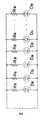
図2は本参考例の光源装置の基本構成を示すものであって、発光色の異なる赤色発光ダイオードチップ1R、緑色発光ダイオードチップ1G、青色発光ダイオードチップ1Bを基板の同一平面上に実装して所望の発光色になるようにそれぞれのチップ面積が設定されている。したがって、所望の発光色になるように各発光ダイオードチップ1R、1G、1Bそれぞれのチップ面積を設定することにより、所望の発光色を高輝度で得ることができる。例えば、図12に示した従来構成において各発光ダイオードDR、DG、DBに流れる電流比を1.5:2.0:1.0として得ていた発光色も各発光ダイオードチップ1R、1G、1Bそれぞれのチップ面積を適宜設定することにより得ることが可能となる。
【0018】
本参考例では、図1に示すように、矩形状の基板10の同一平面上に実装され所望の発光色になるようにそれぞれのチップ面積が設定された1つの赤色発光ダイオードチップ1R、1つの緑色発光ダイオードチップ1G、1つの青色発光ダイオードチップ1Bにより1単位のモジュールMを構成し、複数のモジュールMを同一平面上に配列してある。したがって、本参考例の光源装置は、所望の発光色及び光量を得ることができる面光源を構成し、モジュールMの数を増やすことによって比較的大面積の面光源を提供することができる。また、各モジュールMごとに輝度を異ならせることによって配光を変化させることができる。
【0019】
なお、発光色の異なる赤色発光ダイオードチップ1R、緑色発光ダイオードチップ1G、青色発光ダイオードチップ1Bを複数個ずつ集合させたものを1単位としてモジュールMを構成してもよいことは勿論である。また、モジュールMの形状は図1に示すように矩形状に限らず、形状を適宜変化させて配列することにより任意の形状の面光源を提供することが可能になる。
【0020】
ところで、本参考例では、赤色発光ダイオードチップ1R、緑色発光ダイオードチップ1G、青色発光ダイオードチップ1Bに形成されている発光各発光ダイオードをDR、DG、DBとした場合、図3に示すように各発光ダイオードDR、DG、DBを直列接続し定電流源Iに接続してある。しかして、本参考例の光源装置では、各発光ダイオードDR、DG、DBを直列接続し各発光ダイオードDR、DG、DBに流れる電流の大きさを同じにした場合であっても所望の発光色を得ることができる。
【0021】
また、他の構成例としては、各発光ダイオードDR、DG、DBを図4に示すように、それぞれ限流要素としての抵抗RR、RG、RBを介して並列接続してもよく、この場合には、抵抗RR、RG、RBの抵抗値を変化させることによっても任意の調色が可能になる。しかも、抵抗RR、RG、RBによって発光ダイオードDR、DG、DBに過電流が流れるのを防止することができる。また、図5に示すように、発光ダイオードDR、DG、DBを直列接続し且つ限流要素としての抵抗を直列接続した複数の直列回路を直流電圧源Eに並列接続してもよく、該直列回路を適宜位置に配置することにより、配光を変化させることが可能となる。この場合も抵抗Rによって発光ダイオードDR、DG、DBに過電流が流れるのを防止することができる。
【0022】
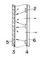
(参考例2)
本参考例の光源装置は、図6に示すように、複数の可視光発光ダイオードチップ1と、これらの可視光発光ダイオードチップ1が同一平面に実装される透明基板6(光透過率の良い透明材料により形成された光透過板)と、透明基板6に設けられ可視光発光ダイオードチップ1へ給電する透明電極4(例えばITOなど)と、透明基板6の実装面側に対向配置され可視光発光ダイオード1の光を反射する光反射板5とを備えている。
【0023】
しかして、本参考例の光源装置では、可視光発光ダイオードチップ1からの光は、光反射板5により反射され、透明電極4及び透明基板6を通して外部へ取り出されるので、可視光発光ダイオードチップ1からの光を効率良く外部へ取り出すことができ、可視光発光ダイオードを利用した従来の面光源に比べて高輝度の面光源を提供することができる。なお、図6中の矢印は、光の経路を例示したものである。
【0024】
(参考例3)
本参考例の光源装置は、図7に示すように、複数の可視光発光ダイオードチップ1と、これら可視光発光ダイオードチップ1が同一平面に実装される透明基板6と、透明基板6に設けられ可視光発光ダイオードチップ1へ給電する透明電極4と、透明基板6の実装面側に対向配置され可視光発光ダイオードチップ1の光の一部を透過させ残りの光を反射する光反射板7とを備えている。
【0025】
しかして、本参考例の光源装置では、可視光発光ダイオードチップ1からの光は、対向配置される光反射板7と透明基板6との両方を通して外部へ取り出されるので、可視光発光ダイオードチップ1からの光を効率良く外部へ取り出すことができ、可視光発光ダイオードを利用した従来の面光源に比べて高輝度の面光源を提供することができる。なお、図7中の矢印は、光の経路を例示したものである。
【0026】
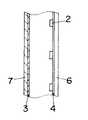
(参考例4)
本参考例の光源装置は、図8に示すように、複数の発光ダイオードチップ2と、これら発光ダイオードチップ2が同一平面に実装される透明基板6と、透明基板6に設けられ発光ダイオードチップ2へ給電する透明電極4と、透明基板6の実装面側に対向配置され発光ダイオードチップ2からの光を反射する光反射板5とを備え、発光ダイオードチップ2からの光を受けて可視光領域の光を発光する蛍光体3が上記光反射板5に設けられている。発光ダイオードチップ2としては紫外域か青色の少なくとも一方の波長域の光を発光するものを用いている。
【0027】
しかして、本参考例の光源装置では、蛍光体3の光を、透明電極4及び透明基板6を通して外部へ取り出すことができ、発光ダイオードチップ2の光を有効に利用して、可視光発光ダイオードを利用した従来の面光源に比べて高輝度の面光源を提供することができる。なお、図8中において実線で示す矢印は、発光ダイオードチップ2からの光の経路を例示したものであり、一点鎖線で示す矢印は、蛍光体3からの光の経路を例示したものである。
【0028】
(参考例5)
本参考例の光源装置は、図9に示すように、複数の発光ダイオードチップ2と、これら発光ダイオードチップ2が実装される透明基板6と、透明基板6に設けられ発光ダイオードチップ2へ給電する透明電極4と、透明基板6の実装面側に対向配置され発光ダイオード2の光の一部を透過させ残りの光を反射する光反射板7(光反射透過板)とを備え、発光ダイオードチップ2からの光を受けて可視光領域の光を発光する蛍光体3が上記光反射板7に設けられている。発光ダイオードチップ2としては紫外域か青色の少なくとも一方の発光域の光を発光するものを用いている。
【0029】
しかして、本参考例の光源装置では、蛍光体3の光を光反射板7と透明基板6との両方を通して外部へ取り出すことができ、発光ダイオードチップ2の光を有効に利用して、可視光発光ダイオードを利用した従来の面光源に比べて高輝度の面光源を提供することができる。
(実施形態1)
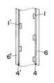
本実施形態の光源装置は、図10に示すように、第1の可視光発光ダイオードチップ1と、第1の可視光発光ダイオードチップ1が実装される第1の透明基板6と、第1の透明基板6に設けられ第1の可視光発光ダイオードチップ1へ給電する第1の透明電極4と、第2の可視光発光ダイオードチップ1’と、第1の透明基板6の実装面側に対向配置され第2の可視光発光ダイオード1’が実装される第2の透明基板6’と、第2の透明基板6’に設けられ第2の可視光発光ダイオードチップ1’へ給電する第2の透明電極4’とを備えている。
【0030】
しかして、本実施形態の光源装置では、可視光発光ダイオードチップ1からの光を第2の透明電極4’及び第2の透明基板6’を通して外部へ取り出すことができ且つ可視光発光ダイオード1’からの光を第1の透明電極4及び第1の透明基板6を通して外部へ取り出すことができるので、可視光発光ダイオードチップ1及び可視光発光ダイオードチップ1’からの光を効率良く外部へ取り出すことができ、可視光発光ダイオードを利用した従来の面光源に比べて高輝度の面光源を提供することができる。
【0031】
(実施形態2)
本実施形態の光源装置は、図11に示すように、第1の発光ダイオードチップ2と、第1の発光ダイオードチップ2が実装される第1の透明基板6と、第1の透明基板6に設けられ第1の発光ダイオードチップ2へ給電する第1の透明電極4と、第2の発光ダイオードチップ2’と、第1の透明基板6の実装面側に対向配置され第2の発光ダイオードチップ2’が実装される第2の透明基板6’と、第2の透明基板6’に設けられ第2の発光ダイオードチップ2’へ給電する第2の透明電極4’とを備え、各透明基板6、6’の実装面側には発光ダイオードチップ2、2’の光を受けて可視光領域の光を発光する蛍光体3が設けられている。発光ダイオードチップ2、2’としては紫外域か青色の少なくとも一方の発光域の光を発光するものを用いている。
【0032】
しかして、本実施形態の光源装置では、蛍光体3の光を透明基板6、6’を通して外部へ取り出すことができ、発光ダイオードチップ2の光を有効に利用して、可視光発光ダイオードを利用した従来の面光源に比べて高輝度の面光源を提供することができる。
なお、参考例2〜5、実施形態1、2において光反射板の反射面が拡散反射性を有するものであってもよい。
【0033】
【発明の効果】
請求項1の発明は、第1の可視光発光ダイオードチップと、第1の可視光発光ダイオードチップが実装される第1の透明基板と、第1の透明基板に設けられ第1の可視光発光ダイオードチップへ給電する第1の透明電極と、第2の可視光発光ダイオードチップと、第1の透明基板の実装面側に対向配置され第2の可視光発光ダイオードチップが実装される第2の透明基板と、第2の透明基板に設けられ第2の可視光発光ダイオードへ給電する第2の透明電極とを備えているので、第1の透明電極及び第1の透明基板を通して第2の可視光発光ダイオードチップの光を外部へ取り出すことができるとともに、第2の透明電極及び第2の透明基板を通して第1の可視光発光ダイオードチップの光を外部へ取り出すことができ、可視光発光ダイオードを利用した従来の面光源に比べて高輝度の面光源を実現することができるという効果がある。
【0041】
請求項2の発明は、第1の発光ダイオードチップと、第1の発光ダイオードチップが実装される第1の透明基板と、第1の透明基板に設けられ第1の発光ダイオードチップへ給電する第1の透明電極と、第2の発光ダイオードチップと、第1の透明基板の実装面側に対向配置され第2の発光ダイオードチップが実装される第2の透明基板と、第2の透明基板に設けられ第2の発光ダイオードへ給電する第2の透明電極とを備え、各透明基板の実装面側には対向する透明基板に実装された発光ダイオードチップの光を受けて可視光領域の光を発光する蛍光体が設けられているので、蛍光体の光を第1の透明基板及び第2の透明基板を通して外部へ取り出すことができ、発光ダイオードチップの光を有効に利用して、可視光発光ダイオードを利用した従来の面光源に比べて高輝度の面光源を実現することができるという効果がある。
【図面の簡単な説明】
【図1】参考例1を示す概略構成図である。
【図2】同上の基本構成の説明図である。
【図3】同上の回路構成の説明図である。
【図4】同上の他の回路構成例の説明図である。
【図5】同上のまた他の回路構成例の説明図である。
【図6】参考例2を示す概略構成図である。
【図7】参考例3を示す概略構成図である。
【図8】参考例4を示す概略構成図である。
【図9】参考例5を示す概略構成図である。
【図10】実施形態1を示す概略構成図である。
【図11】実施形態2を示す概略構成図である。
【図12】従来例を示す回路図である。
【図13】他の従来例を示す回路図である。
【図14】従来例を示す概略構成図である。
【符号の説明】
1R 赤色発光ダイオードチップ
1G 緑色発光ダイオードチップ
1B 青色発光ダイオードチップ
10 基板
M モジュール[0001]
BACKGROUND OF THE INVENTION
The present invention relates to a light source device using a light emitting diode.
[0002]
[Prior art]
2. Description of the Related Art Conventionally, as a light source device using a light emitting diode, a light source device that obtains a desired light emission color by arranging a plurality of light emitting diode chips having different light emission colors on one plane and mixing them has been proposed. In this type of light source device, visible light emitting diode chips having the same chip area and different emission colors are provided. Then, for example, as shown in FIG. 12, a red light-emitting diodeD R, the green light-emitting diodeD G, a blue light-emitting diodeD B connected in parallel, and the light emitting diodeDR, D G, the anode side of eachD B Resistors RR , RG , and RB as current limiting elements are inserted in series, and by appropriately setting the resistance values of the resistors RR , RG , and RB , the respective light emitting diodes DR , DG , and performs the adjustment by dimming-toning the current flowing through the DB.
[0003]
There also, as shown in FIG. 13, a red light-emitting diode DR of the same chiparea, green light emitting diode DG, a blue light-emitting diode DB connected in series, even and that the resistance R as a current limiting element connected in series .
Further, the light source device as a surface light source using a light emitting diode, is configured as shown in FIG. 14, a visible light emitting diode chip 1 (for example, red light-emitting diode DR of the chip, the green light-emitting diode DG chips, blue a chip) of the light emitting diode DB, an
[0004]
[Problems to be solved by the invention]
However, in the conventional structure shown in FIG. 12, the light emitting diode DR, DG, since the same chip area DB, the case of obtaining a desired emission color by color mixing, the light emitting diode DR, DG determines the brightness of the light emission color by the luminance of most brightness smaller light emitting diode of DB, there is desired a problem that sufficient luminance of light emission color can not be obtained.
[0005]
In the conventional configuration shown in FIG. 13, the light emitting diodeDR, D G, and the light emitting diode chip area are the same forD BDR, since D G, equal the current flowing through theD B, toning There was a problem that I could not.
In the conventional configuration shown in FIG. 14, the light from the visible
[0006]
The present invention has been made in view of the above circumstances, an object ofthe inventionof
[0007]
[Means for Solving the Problems]
The invention of
[0015]
According to asecond aspect of the present invention, there is provided a first light emitting diode chip, a first transparent substrate on which the first light emitting diode chip is mounted, a first light emitting diode chip provided on the first transparent substrate and supplying power to the first light emitting diode chip. A first transparent electrode, a second light emitting diode chip, a second transparent substrate on which the second light emitting diode chip is mounted facing the mounting surface side of the first transparent substrate, and a second transparent substrate. A second transparent electrode for supplying power to the second light emitting diode, and receiving light from a light emitting diode chip mounted on the opposing transparent substrate on the mounting surface side of each transparent substrate to receive light in the visible light region It is characterized in that a phosphor emitting light is provided, and the light of the phosphor can be taken out through the first transparent substrate and the second transparent substrate, and the light of the light emitting diode chip is effectively used. Use and visible It is possible to realize a high luminance surface light source as compared with the conventional surface light source using light emitting diodes.
[0017]
DETAILED DESCRIPTION OF THE INVENTION
(ReferenceExample 1)
FIG. 2 shows the basic configuration of the light source device of this reference example. The red light
[0018]
In this reference example, as shown in FIG. 1, one red light
[0019]
It should be noted that the module M may be configured with a unit in which a plurality of red light
[0020]
By the way, inthis reference example, when the light emitting diodes formed on the red light
[0021]
As another configuration example, the light emitting diodeDR, D G, theD B as shown in FIG. 4, the resistanceR R as respective current limitingelement, R G, connected in parallel via theR B In this case, arbitrary toning can be performed by changing the resistance values of the resistors RR , RG , and RB. Moreover, the resistorRR, R G, the light emitting diodeD R byRB, D G, it is possible to prevent the overcurrent from flowing to theD B. Further, as shown in FIG. 5, the light emitting diode DR, DG, may be connected in parallel a plurality of series circuits of resistors connected in series to the DB as connected in series and current-limiting element to a DC voltage source E The light distribution can be changed by arranging the series circuit at an appropriate position. Emitting diode DR in this case by the resistanceR, DG, it is possible to prevent the overcurrent from flowing to the DB.
[0022]
(Reference Example 2)
As shown in FIG. 6,the light source device ofthis reference example includes a plurality of visible light
[0023]
Thus, inthe light source device of thepresent reference example, the light from the visible light
[0024]
(Reference Example 3)
As shown in FIG. 7,the light source device ofthis reference example is provided on a plurality of visible light
[0025]
Thus, inthe light source device of thepresent reference example, the light from the visible light emitting
[0026]
(Reference Example 4)
As shown in FIG. 8,the light source device ofthis reference example includes a plurality of light emitting
[0027]
Thus, inthe light source device of thepresent reference example, the light of the
[0028]
(Reference Example 5)
As shown in FIG. 9,the light source device ofthis reference example has a plurality of light emitting
[0029]
Thus, inthe light source device ofthis reference example, the light of the
(Embodiment1 )
As shown in FIG. 10, the light source device of the present embodiment includes a first visible light emitting
[0030]
Thus, in the light source device of the present embodiment, the light from the visible light emitting
[0031]
(Embodiment2 )
As shown in FIG. 11, the light source device of the present embodiment includes a first light emitting
[0032]
Thus, in the light source device of the present embodiment, the light of the
Incidentally, Reference Examples 2-5, the reflecting surface of the Oite light reflectorto the
[0033]
【The invention's effect】
The invention of
[0041]
According to asecond aspect of the present invention, there is provided a first light emitting diode chip, a first transparent substrate on which the first light emitting diode chip is mounted, a first light emitting diode chip provided on the first transparent substrate and supplying power to the first light emitting diode chip. A first transparent electrode, a second light emitting diode chip, a second transparent substrate on which the second light emitting diode chip is mounted facing the mounting surface side of the first transparent substrate, and a second transparent substrate. A second transparent electrode for supplying power to the second light emitting diode, and receiving light from a light emitting diode chip mounted on the opposing transparent substrate on the mounting surface side of each transparent substrate to receive light in the visible light region Since the phosphor that emits light is provided, the light of the phosphor can be taken out through the first transparent substrate and the second transparent substrate, and the light of the light emitting diode chip is effectively used to emit visible light. Use diode There is an effect that it is possible to realize a high luminance surface light source as compared with the conventional surface light source.
[Brief description of the drawings]
FIG. 1is a schematic configuration diagram showing a referenceexample 1 ;
FIG. 2 is an explanatory diagram of the basic configuration of the above.
FIG. 3 is an explanatory diagram of the circuit configuration of the above.
FIG. 4 is an explanatory diagram of another circuit configuration example same as above.
FIG. 5 is an explanatory diagram of still another circuit configuration example.
6is a schematic configuration diagram showing areference example 2. FIG.
7is a schematic configuration diagram showing areference example 3. FIG.
8is a schematic configuration diagram showing areference example 4. FIG.
9is a schematic configuration diagram showing areference example 5. FIG.
10 is a schematic configuration
FIG. 11 is a schematic configuration diagram showing asecond embodiment.
FIG. 12 is a circuit diagram showing a conventional example.
FIG. 13 is a circuit diagram showing another conventional example.
FIG. 14 is a schematic configuration diagram showing a conventional example.
[Explanation of symbols]
1R red light emitting
Claims (2)
Translated fromJapanesePriority Applications (1)
| Application Number | Priority Date | Filing Date | Title |
|---|---|---|---|
| JP32363697AJP3627478B2 (en) | 1997-11-25 | 1997-11-25 | Light source device |
Applications Claiming Priority (1)
| Application Number | Priority Date | Filing Date | Title |
|---|---|---|---|
| JP32363697AJP3627478B2 (en) | 1997-11-25 | 1997-11-25 | Light source device |
Publications (2)
| Publication Number | Publication Date |
|---|---|
| JPH11162233A JPH11162233A (en) | 1999-06-18 |
| JP3627478B2true JP3627478B2 (en) | 2005-03-09 |
Family
ID=18156945
Family Applications (1)
| Application Number | Title | Priority Date | Filing Date |
|---|---|---|---|
| JP32363697AExpired - Fee RelatedJP3627478B2 (en) | 1997-11-25 | 1997-11-25 | Light source device |
Country Status (1)
| Country | Link |
|---|---|
| JP (1) | JP3627478B2 (en) |
Families Citing this family (42)
| Publication number | Priority date | Publication date | Assignee | Title |
|---|---|---|---|---|
| JP2001028947A (en)* | 1999-07-23 | 2001-02-06 | Yamato Kogyo Kk | Method for raising useful plant |
| GB0011749D0 (en) | 2000-05-17 | 2000-07-05 | Cambridge Display Tech Ltd | Light-eminating devices |
| CN100541813C (en) | 2000-06-23 | 2009-09-16 | 剑桥显示技术有限公司 | Light emitting device |
| AT410266B (en)* | 2000-12-28 | 2003-03-25 | Tridonic Optoelectronics Gmbh | LIGHT SOURCE WITH A LIGHT-EMITTING ELEMENT |
| DE10102585A1 (en)* | 2001-01-20 | 2002-07-25 | Philips Corp Intellectual Pty | Mixed colour luminair with differently coloured light sources and light emission surface |
| JP2004071807A (en)* | 2002-08-06 | 2004-03-04 | Sharp Corp | Lighting device, camera device, and portable device |
| US7554258B2 (en)* | 2002-10-22 | 2009-06-30 | Osram Opto Semiconductors Gmbh | Light source having an LED and a luminescence conversion body and method for producing the luminescence conversion body |
| KR100852579B1 (en)* | 2003-03-31 | 2008-08-14 | 샤프 가부시키가이샤 | Surface illumination device and liquid display device using the same |
| US6974229B2 (en)* | 2003-05-21 | 2005-12-13 | Lumileds Lighting U.S., Llc | Devices for creating brightness profiles |
| ATE507703T1 (en)* | 2004-06-03 | 2011-05-15 | Koninkl Philips Electronics Nv | LIGHT DIODES DRIVEN WITH AC CURRENT |
| KR101090751B1 (en)* | 2004-06-29 | 2011-12-08 | 엘지디스플레이 주식회사 | LCD with a back-light assembly |
| KR100647126B1 (en) | 2005-02-02 | 2006-11-23 | 럭스피아 주식회사 | LED package |
| JP2006302582A (en)* | 2005-04-18 | 2006-11-02 | Sony Corp | Backlight device and color liquid crystal display device |
| JP4822499B2 (en)* | 2005-06-03 | 2011-11-24 | シチズン電子株式会社 | Chip type LED |
| JP4726204B2 (en)* | 2005-06-03 | 2011-07-20 | シチズン電子株式会社 | Chip type LED |
| JP4733434B2 (en)* | 2005-06-03 | 2011-07-27 | シチズン電子株式会社 | Chip type LED |
| JP2006339060A (en)* | 2005-06-03 | 2006-12-14 | Akita Denshi Systems:Kk | Lighting system |
| JP4935004B2 (en) | 2005-07-01 | 2012-05-23 | ソニー株式会社 | Display device |
| JP2007027421A (en)* | 2005-07-15 | 2007-02-01 | Harison Toshiba Lighting Corp | LED package and lighting device |
| US20070019129A1 (en)* | 2005-07-20 | 2007-01-25 | Cree, Inc. | Independent control of light emitting diodes for backlighting of color displays |
| JP4678256B2 (en)* | 2005-08-01 | 2011-04-27 | ソニー株式会社 | Surface light source device and color liquid crystal display device assembly |
| US20090279284A1 (en)* | 2005-10-14 | 2009-11-12 | Sharp Kabushiki Kaisha | Illumination device, light source device used for the same, and liquid crystal display equipped with the illumination device |
| US7789536B2 (en)* | 2005-11-21 | 2010-09-07 | Koninklijke Philips Electronics N.V. | Lighting device |
| JP2007150080A (en)* | 2005-11-29 | 2007-06-14 | Mitsubishi Rayon Co Ltd | Linear light source device |
| KR100691454B1 (en)* | 2005-12-23 | 2007-03-12 | 삼성전기주식회사 | LED backlight unit with side color deviation |
| US20090251922A1 (en)* | 2006-05-30 | 2009-10-08 | Sharp Kabushiki Kaisha | Backlight device and display device using the same |
| EP2082160B1 (en)* | 2006-10-10 | 2013-06-19 | Koninklijke Philips Electronics N.V. | Thin illumination device, display device and luminary device |
| US8018424B2 (en)* | 2006-10-19 | 2011-09-13 | Au Optronics Corporation | Backlight device with zone control |
| KR100966374B1 (en)* | 2007-08-27 | 2010-07-01 | 삼성엘이디 주식회사 | Surface light source using white LED and LCD backlight unit having same |
| JP5056520B2 (en)* | 2008-03-21 | 2012-10-24 | 東芝ライテック株式会社 | Lighting device |
| JP4366431B1 (en)* | 2008-07-30 | 2009-11-18 | シーシーエス株式会社 | Light irradiation device |
| JP2010147190A (en)* | 2008-12-17 | 2010-07-01 | Panasonic Electric Works Co Ltd | Double-sided light-emitting device |
| KR20110006773A (en)* | 2009-07-15 | 2011-01-21 | 삼성전자주식회사 | Display and Television |
| KR101495580B1 (en) | 2010-04-26 | 2015-02-25 | 파나소닉 주식회사 | Leadframe, wiring board, light emitting unit, and illuminating apparatus |
| JP2012022220A (en)* | 2010-07-16 | 2012-02-02 | Eeshikku Kk | Display device |
| JP2011205142A (en)* | 2011-07-12 | 2011-10-13 | Sony Corp | Display device |
| KR101188748B1 (en)* | 2012-07-18 | 2012-10-09 | 지스마트 주식회사 | Transparent display board and manucfacturing method |
| JP6342415B2 (en)* | 2012-12-05 | 2018-06-13 | フィリップス ライティング ホールディング ビー ヴィ | Flat lighting equipment |
| CN107146787B (en)* | 2017-04-19 | 2019-08-09 | 深圳市梓光智能科技有限公司 | A production process of an integrated surface mount light emitting device |
| WO2019066491A1 (en)* | 2017-09-29 | 2019-04-04 | 서울반도체 주식회사 | Light emitting device and display device having same |
| KR102650950B1 (en) | 2017-09-29 | 2024-03-26 | 서울반도체 주식회사 | Light emitting device for display and display apparatus having the same |
| JP7380026B2 (en)* | 2019-09-30 | 2023-11-15 | 東芝ライテック株式会社 | Light source module and lighting device |
- 1997
- 1997-11-25JPJP32363697Apatent/JP3627478B2/ennot_activeExpired - Fee Related
Also Published As
| Publication number | Publication date |
|---|---|
| JPH11162233A (en) | 1999-06-18 |
Similar Documents
| Publication | Publication Date | Title |
|---|---|---|
| JP3627478B2 (en) | Light source device | |
| US6540377B1 (en) | Full-color light source unit | |
| US6834977B2 (en) | Light emitting device | |
| EP0921568B1 (en) | LED Luminaire | |
| JP4944796B2 (en) | Lighting device | |
| US7794098B2 (en) | Light-emitting diode light source and backlight module using the same | |
| CN100386688C (en) | Surface illuminating device and liquid crystal display device having the same | |
| US7309151B2 (en) | Light emitting panel | |
| US20060087866A1 (en) | LED backlight | |
| US20130102097A1 (en) | Multicolor light emitting diodes | |
| JP2001053341A (en) | Surface-emitting display | |
| WO2007016110A2 (en) | Acicular ito for led array | |
| JP3454123B2 (en) | LED lighting module | |
| JP2001177156A (en) | Side emitting led lamp | |
| US7375384B2 (en) | Side structure of a bare LED and backlight module thereof | |
| CN1937222A (en) | LED package and illuminating device | |
| US11193635B2 (en) | Flexible and cuttable LED sheet | |
| JP2000275636A (en) | Light source, lighting device, and liquid crystal device using the lighting device | |
| JP2005117028A (en) | LED lighting source | |
| JP3530442B2 (en) | Chromaticity adjustment method for surface light source device | |
| JP2011023295A (en) | Led lighting device and image display apparatus | |
| JP2003150074A (en) | Led module and led display device | |
| JP4028985B2 (en) | Backlight unit | |
| KR102671003B1 (en) | Backlight module with mjt led and backlight unit having the same | |
| JP2001006416A (en) | Backlight structure |
Legal Events
| Date | Code | Title | Description |
|---|---|---|---|
| A977 | Report on retrieval | Free format text:JAPANESE INTERMEDIATE CODE: A971007 Effective date:20031216 | |
| A131 | Notification of reasons for refusal | Free format text:JAPANESE INTERMEDIATE CODE: A131 Effective date:20031224 | |
| A521 | Written amendment | Free format text:JAPANESE INTERMEDIATE CODE: A523 Effective date:20040223 | |
| A131 | Notification of reasons for refusal | Free format text:JAPANESE INTERMEDIATE CODE: A131 Effective date:20040817 | |
| A521 | Written amendment | Free format text:JAPANESE INTERMEDIATE CODE: A523 Effective date:20041018 | |
| TRDD | Decision of grant or rejection written | ||
| A01 | Written decision to grant a patent or to grant a registration (utility model) | Free format text:JAPANESE INTERMEDIATE CODE: A01 Effective date:20041116 | |
| A61 | First payment of annual fees (during grant procedure) | Free format text:JAPANESE INTERMEDIATE CODE: A61 Effective date:20041129 | |
| FPAY | Renewal fee payment (event date is renewal date of database) | Free format text:PAYMENT UNTIL: 20071217 Year of fee payment:3 | |
| FPAY | Renewal fee payment (event date is renewal date of database) | Free format text:PAYMENT UNTIL: 20081217 Year of fee payment:4 | |
| FPAY | Renewal fee payment (event date is renewal date of database) | Free format text:PAYMENT UNTIL: 20081217 Year of fee payment:4 | |
| S533 | Written request for registration of change of name | Free format text:JAPANESE INTERMEDIATE CODE: R313533 | |
| FPAY | Renewal fee payment (event date is renewal date of database) | Free format text:PAYMENT UNTIL: 20081217 Year of fee payment:4 | |
| R350 | Written notification of registration of transfer | Free format text:JAPANESE INTERMEDIATE CODE: R350 | |
| FPAY | Renewal fee payment (event date is renewal date of database) | Free format text:PAYMENT UNTIL: 20091217 Year of fee payment:5 | |
| FPAY | Renewal fee payment (event date is renewal date of database) | Free format text:PAYMENT UNTIL: 20091217 Year of fee payment:5 | |
| FPAY | Renewal fee payment (event date is renewal date of database) | Free format text:PAYMENT UNTIL: 20101217 Year of fee payment:6 | |
| LAPS | Cancellation because of no payment of annual fees |