JP3625197B2 - Plasma apparatus and plasma generation method - Google Patents
Plasma apparatus and plasma generation methodDownload PDFInfo
- Publication number
- JP3625197B2 JP3625197B2JP2001247853AJP2001247853AJP3625197B2JP 3625197 B2JP3625197 B2JP 3625197B2JP 2001247853 AJP2001247853 AJP 2001247853AJP 2001247853 AJP2001247853 AJP 2001247853AJP 3625197 B2JP3625197 B2JP 3625197B2
- Authority
- JP
- Japan
- Prior art keywords
- electromagnetic field
- cavity
- waveguide
- conductor
- conductor member
- Prior art date
- Legal status (The legal status is an assumption and is not a legal conclusion. Google has not performed a legal analysis and makes no representation as to the accuracy of the status listed.)
- Expired - Fee Related
Links
- 238000000034methodMethods0.000titleclaimsdescription30
- 239000004020conductorSubstances0.000claimsdescription302
- 230000005672electromagnetic fieldEffects0.000claimsdescription249
- 230000001902propagating effectEffects0.000claimsdescription14
- 230000004323axial lengthEffects0.000claimsdescription3
- 238000010586diagramMethods0.000description29
- 238000009826distributionMethods0.000description21
- 230000005684electric fieldEffects0.000description16
- 239000000758substrateSubstances0.000description8
- 230000010287polarizationEffects0.000description6
- 230000004048modificationEffects0.000description5
- 238000012986modificationMethods0.000description5
- 230000003111delayed effectEffects0.000description4
- 230000002093peripheral effectEffects0.000description4
- 230000008569processEffects0.000description4
- 238000006243chemical reactionMethods0.000description3
- 230000000694effectsEffects0.000description3
- 239000004065semiconductorSubstances0.000description3
- 230000008859changeEffects0.000description2
- 230000002349favourable effectEffects0.000description2
- 239000000463materialSubstances0.000description2
- 230000007246mechanismEffects0.000description2
- 238000007789sealingMethods0.000description2
- RYGMFSIKBFXOCR-UHFFFAOYSA-NCopperChemical compound[Cu]RYGMFSIKBFXOCR-UHFFFAOYSA-N0.000description1
- 241000733322PlateaSpecies0.000description1
- VYPSYNLAJGMNEJ-UHFFFAOYSA-NSilicium dioxideChemical compoundO=[Si]=OVYPSYNLAJGMNEJ-UHFFFAOYSA-N0.000description1
- 238000010521absorption reactionMethods0.000description1
- 229910052782aluminiumInorganic materials0.000description1
- XAGFODPZIPBFFR-UHFFFAOYSA-NaluminiumChemical compound[Al]XAGFODPZIPBFFR-UHFFFAOYSA-N0.000description1
- 238000004380ashingMethods0.000description1
- 230000015572biosynthetic processEffects0.000description1
- 238000005266castingMethods0.000description1
- 239000000919ceramicSubstances0.000description1
- 229910052802copperInorganic materials0.000description1
- 239000010949copperSubstances0.000description1
- 239000013078crystalSubstances0.000description1
- 238000005520cutting processMethods0.000description1
- 230000003247decreasing effectEffects0.000description1
- 238000005530etchingMethods0.000description1
- 230000005284excitationEffects0.000description1
- 239000012212insulatorSubstances0.000description1
- 230000003993interactionEffects0.000description1
- 238000004519manufacturing processMethods0.000description1
- 229910052751metalInorganic materials0.000description1
- 239000002184metalSubstances0.000description1
- 230000000644propagated effectEffects0.000description1
- 230000002441reversible effectEffects0.000description1
Images


Classifications
- H—ELECTRICITY
- H01—ELECTRIC ELEMENTS
- H01J—ELECTRIC DISCHARGE TUBES OR DISCHARGE LAMPS
- H01J37/00—Discharge tubes with provision for introducing objects or material to be exposed to the discharge, e.g. for the purpose of examination or processing thereof
- H01J37/32—Gas-filled discharge tubes
- H01J37/32009—Arrangements for generation of plasma specially adapted for examination or treatment of objects, e.g. plasma sources
- H01J37/32192—Microwave generated discharge
- H01J37/32211—Means for coupling power to the plasma
- H01J37/3222—Antennas
- H—ELECTRICITY
- H01—ELECTRIC ELEMENTS
- H01J—ELECTRIC DISCHARGE TUBES OR DISCHARGE LAMPS
- H01J37/00—Discharge tubes with provision for introducing objects or material to be exposed to the discharge, e.g. for the purpose of examination or processing thereof
- H01J37/32—Gas-filled discharge tubes
- H01J37/32009—Arrangements for generation of plasma specially adapted for examination or treatment of objects, e.g. plasma sources
- H01J37/32192—Microwave generated discharge
- H01J37/32211—Means for coupling power to the plasma
- H01J37/32229—Waveguides
- H—ELECTRICITY
- H01—ELECTRIC ELEMENTS
- H01J—ELECTRIC DISCHARGE TUBES OR DISCHARGE LAMPS
- H01J37/00—Discharge tubes with provision for introducing objects or material to be exposed to the discharge, e.g. for the purpose of examination or processing thereof
- H01J37/32—Gas-filled discharge tubes
- H01J37/32431—Constructional details of the reactor
- H01J37/3244—Gas supply means
Landscapes
- Physics & Mathematics (AREA)
- Engineering & Computer Science (AREA)
- Plasma & Fusion (AREA)
- Chemical & Material Sciences (AREA)
- Analytical Chemistry (AREA)
- Plasma Technology (AREA)
- Chemical Vapour Deposition (AREA)
- Drying Of Semiconductors (AREA)
Description
Translated fromJapanese【0001】
【発明の属する技術分野】
本発明は、スロットアンテナを用いて処理容器内に供給した電磁界によりプラズマを生成するプラズマ装置およびプラズマ生成方法に関する。
【0002】
【従来の技術】
半導体装置やフラットパネルディスプレイの製造において、酸化膜の形成や半導体層の結晶成長、エッチング、またアッシングなどの処理を行うために、プラズマ装置が多用されている。これらのプラズマ装置の中に、スロットアンテナを用いて処理容器内に高周波電磁界を供給し、その電磁界により高密度プラズマを発生させる高周波プラズマ装置がある。この高周波プラズマ装置は、プラズマガスの圧力が比較的低くても安定してプラズマを生成することができるという特色がある。
このようなプラズマ装置を用いて各種処理を行う際には、半導体基板等の処理面上におけるプラズマの二次元的な分布(以下「面内分布」という)を均一にする必要がある。
【0003】
スロットアンテナを用いて均一な面内分布を有するプラズマを生成する方法として、高周波電源から給電される高周波電磁界を回転電磁界に変換し、円偏波になされた回転高周波電磁界をスロットアンテナに供給することが考えられている。
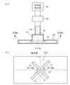
図21は、従来の高周波プラズマ装置の一構成例を示す図である。この図21においては、従来の高周波プラズマ装置の一部構成について縦断面構造が示されている。
【0004】
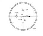
従来のプラズマ装置は、上部が開口した有底円筒形の処理容器111と、この処理容器111の上部開口を塞ぐ誘電体板113と、この誘電体板113の上に配置され、処理容器111内に高周波電磁界を放射するラジアルアンテナ130とを備えている。
この処理容器111の底部には基板台122が固定され、この基板台122の載置面に被処理体である基板121が配置される。また、処理容器111の底部には、真空排気用の排気口116が設けられ、処理容器111の側壁には、プラズマガスおよびプロセスガス供給用のノズル117が設けられている。
誘電体板113は、石英ガラス等からなり、処理容器111との間にOリングなどのシール部材(図示せず)を介在させることにより、処理容器111内のプラズマが外部に漏れないようにしている。
【0005】
また、ラジアルアンテナ130は、スロットアンテナの一種であり、ラジアル導波路133を形成する互いに平行な2枚の円形導体板131,132と、これらの導体板131,132の外周部を接続する導体リング134とから構成されている。ラジアル導波路133の上面となる導体板132の中心部には、高周波電磁界をラジアルアンテナ130内に導入する導入口135が形成されている。ラジアル導波路133の下面となる導体板131には、ラジアル導波路133内を伝搬する電磁界Fを誘電体板113を介して処理容器111内に放射するスロット136が周方向に複数形成されて、ラジアルアンテナ130のアンテナ面を形成している。さらに、ラジアルアンテナ130および誘電体板113の外周は環状のシールド材112によって覆われ、電磁界が外部に漏れない構造になっている。
【0006】
従来のプラズマ装置においては、次のような構成をとることによって、ラジアルアンテナ130に回転電磁界を供給していた。
すなわち、従来のプラズマ装置は、回転電磁界を供給するために、高周波電磁界を発生する高周波発生器145と、高周波発生器145から出力される高周波電磁界を導く矩形導波管143と、矩形導波管と円筒導波管とを接続するための矩形・円筒変換器147と、直線偏波の高周波電磁界を回転電磁界に変換する円偏波変換器146とを備えていた。
【0007】
ここで円偏波変換器146としては、例えば、図22(c)に示すように円筒導波管の内壁に対向する導体製の円柱状突起146Aを軸方向に1組または複数組設けたものが用いられる。これら円柱状突起146Aは、矩形・円筒変換器147より入力されるTE11モードの電磁界の電界の主方向に対して45°をなす方向に配置され、複数組の場合には軸方向にλ/4(λは伝搬する電磁波の管内波長)の間隔で設けられて、このTE11モードの高周波電磁界をその電界の主方向が円筒導波管の軸線を中心に回転する回転電磁界に変換する。
【0008】
このような構成を有する従来のプラズマ装置において回転電磁界が供給される仕組みを図22を参照して説明すると次のようになる。なお、図22は、矩形導波管143、矩形・円筒変換器147、円偏波変換器146の内部を伝搬する電磁界の様子を模式的に表す図である。ここで図22(a)は、図21に示した矩形導波管143を伝搬する電磁界のA−A’における電界の様子、図22(b)、(e)、(f)は、矩形・円筒変換器147の出口B−B’における電界の様子、図22(c)、(d)、(g)は、円偏波変換器146を伝搬する電磁界の電界と回転の方向を示す。
【0009】
高周波発生器145よりTE10モードで矩形導波管143を伝搬した高周波電磁界(図22(a))は、矩形・円筒変換器147によってTE11モードに変換され(図22(b))円偏波変換器の146の円筒導波管に導入される。そして円偏波変換器146を伝搬しながら回転電磁界に変換され(図22(c))、導体板132の中心部に形成された導入口135よりラジアルアンテナ130内に供給される。
【0010】
【発明が解決しようとする課題】
しかしながら、ラジアルアンテナ130に供給された回転電磁界の一部はラジアル導波路133の端部に位置する導体リング134によって反射され、その反射された回転電磁界が同じ向きに回転しながら円偏波変換器146内を逆向きに伝搬する(図22(d))。そして、この反射電磁界は矩形・円筒変換器147において固定端の反射を行い(図22(e)、(f))、今度は逆方向に回転する回転電磁界となって円偏波変換器146内を伝搬し(図22(g))、ラジアルアンテナ130に供給されることとなる。
【0011】
その結果、ラジアルアンテナ130には位相および回転の向きが互いに異なる回転電磁界が混在した状態で供給されることとなり、そのときの高周波電磁界の偏波は、図23に示すような楕円となる。すると、処理容器内で生成されるプラズマの面内分布の均一性が低下して、特に周縁部でのプラズマ処理にむらが生じることとなる。
このように円偏波変換器146で変換した回転電磁界をラジアルアンテナ130に供給しただけでは、ラジアルアンテナ130からの反射電磁界の影響により、プラズマ分布の面内均一性を得ることが困難であった。
本発明はこのような課題を解決するためになされたものであり、その目的は、プラズマ分布の面内均一性を改善することにある。
【0012】
【課題を解決するための手段】
本発明にかかるプラズマ装置は、被処理体を収容する処理容器と、対向する第1および第2の導体板から形成されるラジアル導波路と、前記第1の導体板の中心部に接続され、共振器を構成するとともに給電される高周波電磁界を回転電磁界に変換して前記ラジアル導波路に供給するキャビティと、前記ラジアル導波路の内部における前記キャビティの開口部の周囲に設けられ、前記キャビティの内径と同じ内径を有するリング部材と、前記第2の導体板に形成され、前記ラジアル導波路を伝搬する前記高周波電磁界を前記処理容器に供給するスロットとを備えることを特徴とする。
本発明においては、キャビティ内において回転電磁界が共振しながらラジアル導波路内に円偏波になされた回転高周波電磁界が供給される。
また、リング部材の厚みと幅を調節することによって、キャビティ内で共振する高周波電磁界のうち、ラジアル導波路内に供給される高周波電磁界の割合を調節することができる。
【0014】
本発明にかかるプラズマ装置の第1の構成例として、上記キャビティは、前記高周波電磁界を給電する同軸導波管の外部導体と接続された円形導体部材と、一端がこの円形導体部材と接続され他端が前記ラジアル導波路に開口した円筒導体部材とから形成されるとともに、前記円形導体部材の中心からその径方向に離間した位置に設けられ前記同軸導波管の内部導体と一端が接続された給電ピンと、この給電ピンと前記円形導体部材の中心を挟んで所定の角度をなす位置に設けられ一端が前記円形導体部材と接続された摂動ピンとを備えることを特徴とする。
このような構成においては、同軸導波管を介して給電される高周波電磁界は、給電ピンと摂動ピンとの相互作用によって回転磁界に変換され、キャビティ内で共振しながらラジアル導波路内に供給される。
【0015】
ここで給電ピンの他端は、開放状態になっていてもよいし、スロットが形成された第2の導体板に接続されていてもよい。
給電ピンの他端が第2の導体板に接続されている場合、その給電ピンの他端に、第2の導体板の側に広がる円錐台状の導電部材が設けられていてもよい。このような形状をした導体部材を用いることにより、キャビティ内で共振する高周波電磁界をラジアル導波路内に導入し易くすることができる。
摂動ピンの他端もまた、開放状態になっていてもよいし、第2の導体板に接続されていてもよい。また、円筒導体部材に接続されていてもよい。
【0016】
また、給電ピンの他端が、円筒導体部材に接続されていてもよい。
この場合、摂動ピンの他端が、スロットが形成された第2の導体板に接続されていてもよいし、円筒導体部材に接続されていてもよい。
【0017】
本発明にかかるプラズマ装置の第2の構成例として、上記キャビティは、前記高周波電磁界を給電する同軸導波管の外部導体と接続された円形導体部材と、一端がこの円形導体部材と接続され他端が前記ラジアル導波路に開口した円筒導体部材と、この円筒導体部材の側壁内部に対向配置された導電部材とから形成されるとともに、前記円形導体部材の中心からその径方向に離間した位置に設けられ前記同軸導波管の内部導体と一端が接続された給電ピンを備えることを特徴とする。
このような構成において、キャビティは、前記円筒導体部材の側壁内部に対向配置された導電部材によって、その円筒導体部材の軸に垂直な断面が互いに対向する切り欠き部を有するように形成される。その結果、同軸導波管を介して給電される高周波電磁界はキャビティ内で回転電磁界に変換され、共振しながらラジアル導波路内に供給される。
【0018】
ここで前記円筒導体部材の側壁内部に対向配置された導電部材は、この円筒導体部材の一端から他端まで延在していてもよい。
また、導電部材は、円筒導体部材の軸方向の長さが、高周波電磁界の波長の略1/4であってもよい。この場合、導電部材と給電ピンとの平行部分の長さが上記高周波電磁界の波長の略1/4となり、キャビティ内に良好な回転電磁界を得られる。
また、導電部材は、ラジアル導波路の側の端部が、スロープ状に成形されていてもよい。このように成形することにより、キャビティ内において導電部材が存在する領域と存在しない領域とのインピーダンスの変化を緩やかにして、2つの領域の境界での高周波電磁界の反射を抑制することができる。
導電部材の端部をスロープ状に成形する場合、その端部を除く本体は、円筒導体部材の軸方向の長さが、高周波電磁界の波長の略1/4であってもよい。これにより、キャビティ内に良好な回転電磁界を得られる。
また、給電ピンの他端は、スロットが形成された第2の導体板に接続されていてもよいし、円形導体部材から円筒導体部材の軸方向に高周波電磁界の波長の略1/4離れた位置で導体部材に接続されていてもよい。
なお、円筒導体部材の側壁内部に設けられる導電部材として、互いに対向する1組または複数組の導体製の円柱状突起を軸方向に設けてもよい。
【0019】
本発明にかかるプラズマ装置の第3の構成例として、上記キャビティは、前記高周波電磁界を給電する同軸導波管の外部導体と接続された楕円形導体部材と、一端がこの楕円形導体部材と接続され他端が前記ラジアル導波路に開口し、断面が楕円形状の筒状導体部材とから形成されるとともに、前記楕円形導体部材の中心からその径方向に離間しかつその長径および短径と所定の角度をなす位置に設けられ前記同軸導波管の内部導体と接続された給電ピンとを備えることを特徴とする。
このような構成において、同軸導波管を介して給電される高周波電磁界は、楕円形の断面を有するキャビティ内で回転電磁界に変換され、共振しながらラジアル導波路内に供給される。
ここで給電ピンの他端は、スロットが形成された第2の導体板に接続されていてもよし、円形導体部材から円筒導体部材の軸方向に高周波電磁界の波長の略1/4離れた位置で導体部材に接続されていてもよい。
【0020】
本発明にかかるプラズマ装置の第4の構成例として、上記キャビティは、前記高周波電磁界を給電する第1、第2の同軸導波管の外部導体と接続された円形導体部材と、一端がこの円形導体部材と接続され他端が前記ラジアル導波路に開口した円筒導体部材とから形成されるとともに、前記円形導体部材の中心からその径方向に離間した位置に設けられ前記第1の同軸導波管の内部導体と接続された第1の給電ピンと、この第1の給電ピンと前記円形導体部材の中心を挟んで所定の角度をなす位置に設けられ前記第2の同軸導波管の内部導体と接続された第2の給電ピンとを備えることを特徴とする。
このような構成において、第1、第2の給電ピンに位相の異なる高周波電磁界を給電することによって回転電磁界が生成され、この回転電磁界がキャビティ内で共振しながらラジアル導波路内に供給される。
ここで第1,第2の給電ピンのそれぞれの他端は、スロットが形成された第2の導体板に接続されていてもよいし、円形導体部材から円筒導体部材の軸方向に高周波電磁界の波長の略1/4離れた位置で導体部材に接続されていてもよい。
【0021】
本発明にかかるプラズマ装置の第5の構成例として、上記キャビティは、高周波電磁界を給電する少なくとも1本の同軸導波管の外部導体と接続された円形導体部材と、一端がこの円形導体部材と接続され他端がラジアル導波路に開口した円筒導体部材とから形成されるとともに、少なくとも1本の同軸導波管より給電された高周波電磁界を回転電磁界としてキャビティ内に放射するパッチアンテナを備え、このパッチアンテナは、円形導体部材と、この円形導体部材と所定の間隔をもって対向配置され少なくとも1本の同軸導波管の内部導体と接続された導体板とを含むことを特徴とする。
このような構成において、同軸導波管を介して給電される高周波電磁界は、パッチアンテナによって回転電磁界としてキャビティ内に放射され、共振しながらラジアル導波路内に供給される。
【0022】
さらに、本発明にかかるプラズマ装置の第6の構成例として、上記キャビティは、高周波電磁界を給電する矩形導波管の一側面または終端面と、一端がこの矩形導波管の一側面または終端面と接続され他端がラジアル導波路に開口した円筒導体部材とから形成され、上記矩形導波管の一側面または終端面には、高周波電磁界を回転電磁界としてキャビティ内に放射する複数のスロットが形成されていることを特徴とする。
このような構成において、矩形導波管を介して給電される高周波電磁界は、その矩形導波管の一側面または終端面に形成された複数のスロットによって回転電磁界としてキャビティ内に放射され、共振しながらラジアル導波路内に供給される。
ここで複数のスロットは、互いの中点で交差する2本のスロットであってもよい。この2本のスロットによって構成されるスロットをクロススロットと呼ぶ。
また複数のスロットは、互いに離間して配置された互いに略垂直な方向にのびる2本のスロットであってもよい。この2本のスロットによって構成されるスロットをハの字スロットと呼ぶ。
【0023】
また、本発明にかかるプラズマ生成方法は、共振器を構成するキャビティに高周波電磁界を給電し、この高周波電磁界を回転電磁界に変換するとともに前記キャビティ内で共振させながら、回転電磁界に変換された高周波電磁界をラジアル導波路に供給し、前記ラジアル導波路を伝搬する前記高周波電磁界を前記ラジアル導波路に形成されたスロットを介して処理容器内に供給し、前記処理容器内に供給された前記高周波電磁界によってプラズマを生成するプラズマ生成方法であって、前記ラジアル導波路の内部における前記キャビティの開口部の周囲に設けられたリング部材によって、前記キャビティ内で共振する前記高周波電磁界のうち前記ラジアル導波路に供給される前記高周波電磁界の割合を調整することを特徴とする。
この方法においては、回転電磁界を共振させながらラジアル導波路に供給することによって、ラジアル導波路に供給される高周波電磁界を円偏波になされた回転電磁界とすることができる。
【0024】
本発明にかかるプラズマ生成方法の第1の構成例は、共振器を構成するキャビティ内に給電ピンと摂動ピンを設けることによって、同軸導波管を介して給電された高周波電磁界を回転電磁界に変換しかつキャビティ内で共振させるものである。
【0025】
また、本発明にかかるプラズマ生成方法の第2の構成例は、高周波電磁界の伝搬方向に垂直な断面が互いに対向する切り欠きを有するキャビティに同軸導波管を介して高周波電磁界を給電することにより、これを回転電磁界に変換しかつキャビティ内で共振させるものである。
【0026】
また、本発明にかかるプラズマ生成方法の第3の構成例は、高周波電磁界の伝搬方向に垂直な断面が楕円形状のキャビティに同軸導波管を介して高周波電磁界を給電することにより、これを回転電磁界に変換しかつキャビティ内で共振させるものである。
【0027】
また、本発明にかかるプラズマ生成方法の第4の構成例は、共振器を構成するキャビティに第1、第2の同軸導波管を介して互いに位相が90°異なる高周波電磁界を給電することによって、回転電磁界を生成しかつキャビティ内で共振させるものである。
【0028】
また、本発明にかかるプラズマ生成方法の第5の構成例は、同軸導波管を介してパッチアンテナに高周波電磁界を給電することにより、キャビティ内に回転電磁界を生成するものである。
【0029】
さらに、本発明にかかるプラズマ生成方法の第6の構成例は、矩形導波管より給電された高周波電磁界を、その矩形導波管の一側面または終端面に形成された複数のスロットからキャビティ内に放射することにより、回転電磁界を生成するものである。
【0030】
【発明の実施の形態】
以下、図面を参照して本発明の実施の形態を説明する。
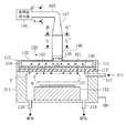
図1乃至図3は、本発明の第1の実施の形態にかかるプラズマ装置を説明する図である。
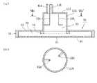
このプラズマ装置は、図1(a)に示すように、上部が開口した有底円筒形の処理容器11と、この処理容器11の上部開口を塞ぐ誘電体板13と、この誘電体板13の上に配置され、処理容器11内に高周波電磁界を放射(またはリーク)するラジアルアンテナ30と、ラジアルアンテナ30および誘電体板13の外周を覆うシールド材12とを備えている。なお、処理容器11と誘電体板13との間にはOリングなどのシール部材14を介在させ、処理容器11内の真空を保つとともにプラズマが外部に漏れないようにしている。
【0031】
この処理容器11の内部には、被処理体である基板21を載置する基板台22が昇降軸23を介して昇降可能に設けられている。この基板台22は、マッチングボックス25を介してバイアス用高周波電源26と電気的に接続されている。なお、処理容器11の気密性を保つため、基板台22底面と処理容器11底面に設けられた絶縁体板15とに結合されたベローズ24が昇降軸23の周囲に設けられている。
この処理容器11には、さらに、真空排気用の排気口16とプラズマガスおよびプロセスガス供給用のノズル17が設けられている。
【0032】
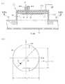
一方、ラジアルアンテナ30は、ラジアル導波路33を形成する互いに平行な2枚の円形導体板31,32と、これらの導体板31,32の外周部を接続する導体リング34とから構成されている。
ここで図1(a)に示すプラズマ装置のIb−Ib’線における断面図を図1(b)に示す。ラジアル導波路33の下面となる導体板31には、例えば図1(b)に示すように、スロット36が周方向に複数形成され、ラジアルアンテナ30のアンテナ面を形成している。
また、ラジアル導波路33の上面となる導体板32の中心部には、後述する給電部が設けられている。
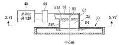
【0033】
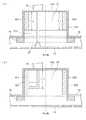
図1(a)に示すように、高周波発生器45において発生した高周波電磁界は、マッチング回路44を介して矩形導波管43を伝搬し、矩形・同軸変換器42においてTE10モードからTEMモードに変換され、同軸導波管41を介してラジアルアンテナ30の給電部に給電される。
【0034】
本実施の形態においてこの給電部は、高周波電磁界を給電する同軸導波管41の外部導体41Aと接続された円形導体部材51Aと、一端がこの円形導体部材51Aと接続され、他端がラジアルアンテナ30内に開口した円筒導体部材51Bとから形成されるキャビティ35と、このキャビティ35内に設けられ、一端が同軸導波管41の内部導体41Bと接続され他端が開放状態となっている給電ピン52と、一端が円形導体部材51Aと接続され他端が開放状態となっている摂動ピン53とからなる。給電ピン52と摂動ピン53は、同軸導波管41を介して供給される電磁界を回転電磁界に変換する。なお、図1(c)は、図1(a)のIc−Ic’線における断面図である。
【0035】
このキャビティ35は、ラジアルアンテナ30の導体板31とともに共振器を構成し、キャビティ35内で共振する高周波電磁界の一部がラジアル導波路33に供給される。
ラジアルアンテナ30の導体板32の中央に設けられたキャビティ35の開口部の周囲には、円筒導体部材51Bの内径(すなわちキャビティ35の内径)と同じ内径を有するリング部材54が配設されている。このリング部材54の厚みと幅を調節することによって、キャビティ35内で共振する高周波電磁界のうち、ラジアル導波路33に供給される高周波電磁界の割合を調節することができる。
なお、キャビティ35に供給された電磁界のうち、共振してキャビティ35内に残る電磁界のエネルギーをキャビティ35からラジアル導波路33に供給される電磁界のエネルギーで割った値は「Q値」と呼ばれる。
【0036】
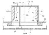
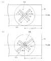
図2を参照して、このような給電部の構成を詳述する。
図2(a)は、側面から見た場合の給電部を表す模式図、図2(b)は、給電ピン52と摂動ピン53の配置を示す模式図である。
本実施の形態においては、高周波発生器45より2.45GHzの高周波電磁界を給電するものとすると、円筒形のキャビティ35の中心軸(以下「中心軸」という)から円筒導体部材51Bの内面までの距離(以下、「キャビティの半径」という)aを、約7.3〜7.5cm、円形導体部材51Aとラジアルアンテナ30の円形導体板31との距離(以下、「キャビティの深さ」という)dを、約3.6cmとすることができる。なお、このときのラジアルアンテナ30の直径は約48cm、導体板31,32間の距離である高さhは1.5〜1.6cmである。
円筒導体部材51Bとともにキャビティ35を形成するリング部材54の幅cは約3.1cmであり、これは電磁波の波長の約1/4に相当する。
また、同軸導波管41の内部導体41Bと接続された給電ピン52の長さl1を1.75〜2.6cm、摂動ピン53の長さl2を1.75〜2.1cmとすることができる。このとき、給電ピン52を摂動ピン53よりも若干長めに設計するとよい。
【0037】
なお、ピン52,53を長くし、または、キャビティ35を深くすると、キャビティ35のQ値は大きくなり、ラジアル導波路33に供給される電磁界の割合を小さくすることができる。プラズマ装置としての用途にはQ値は約30が目安となる。
【0038】
一方、給電ピン52と摂動ピン53は、図2(b)に示すように、ともに円形導体部材51Aの中心軸からb1=b2=約3.6cmの位置に、その中心を挟んで45°の奇数倍、例えばφ=135°の角度をなすように配置されている。これによって、同軸導波管41を介して給電される高周波電磁界は、キャビティ35内においてTMモードの回転電磁界に変換される。
【0039】
ここで示した給電部の寸法は反射係数(VS)を重視して設計した結果得られたものであり、これに限定されないことは言うまでもない。例えば回転電磁界の軸比を重視する場合には、図2において、a=約7.3cm、d=約3.5cm、c=約2.6cm、t=約1.0cm、l1=l2=約1.5cm、b1=約4.3cm、b2=約4.4cmの位置に、φ=115°とするとよい。
【0040】
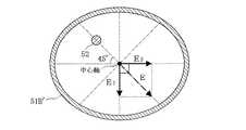
図3を参照すると、給電ピン52と摂動ピン53によって回転電磁界を生成する仕組みは次のように説明することができる。
仮に摂動ピン53が無ければ、給電ピン52によって生じる電界は図3に示すE(点線)のようになり、回転電磁界を得ることはできない。
これに対し、摂動ピン53を設けた場合には、上記電界Eのうち、摂動ピン53方向の成分E1 は、給電ピン52と摂動ピン53との間の容量成分の影響により、位相が遅れる。この位相遅れが90°となるように給電ピン52、摂動ピン53の長さを調整することにより、TM11モードの回転電磁界を得ることができる。
【0041】
したがって、このようなプラズマ装置において、高周波発生器45より発生した高周波電磁界は、同軸導波管41を介して上記キャビティ35に給電され、給電ピン52と摂動ピン53とによって回転電磁界に変換されると同時に、上記キャビティ35において共振しながら、その一部がラジアルアンテナ30のラジアル導波路33に供給される。ラジアルアンテナ30内に供給された高周波電磁界は、ラジアル導波路33を伝搬し、このラジアル導波路33内を伝搬する電磁界Fがこれらのスロット36から処理容器11内に放射(またはリーク)され、ノズル17を通じて処理容器11内に導入されるプラズマガスを電離させてプラズマSを生成する。
【0042】
このときキャビティ35において回転電磁界は共振しているので、キャビティ35内の回転電磁界がラジアル導波路33に供給される。したがって、給電ピン52と摂動ピン53によって高周波電磁界を円偏波に変換することによって、ラジアルアンテナ30から良好な円偏波高周波電磁界を処理容器11内に放射(またはリーク)し、生成されるプラズマSの面内分布の均一性を向上させることができる。
【0043】
本実施の形態では、一端が同軸導波管41の内部導体41Bに接続された給電ピン52の他端(先端)を開放状態とし電圧モードで電磁界を励起するため、給電ピン52の先端において電圧振幅が最大となる。このため、数kW〜数十kWという高電力で給電する場合には、給電ピン52の先端と、摂動ピン53の先端、キャビティ35の円筒導体部材51Bまたはラジアルアンテナ30の導体板31との間で放電が起きないように、給電部を設計することが望ましい。放電を抑制するには、給電ピン52の先端から摂動ピン53の先端、円筒導体部材51Bまたは導体板31までの距離を大きくすればよく、例えば給電ピン52と摂動ピン53については、両者を異なる長さとしてもよい。
【0044】
次に本発明の第2の実施の形態について、図4を参照して説明する。なお、第1の実施の形態と共通する部材については同一の符号を用い、その説明を省略する。
上述した第1の実施の形態では、キャビティ35内に設けられた給電ピン52の先端が開放状態となっているのに対し、この第2の実施の形態にかかるプラズマ装置では、給電ピン52Aの先端が短絡状態となっている。すなわち、図4に示すように、給電ピン52Aの一端は同軸導波管41の内部導体41Bに接続され、先端をなす他端はラジアルアンテナ30のアンテナ面である導体板31と接続され、短絡状態となっている。
キャビティ35の円形導体部材51Aとラジアルアンテナ30の導体板31との距離であるキャビティ35の深さdはλ/2程度とする。先端が導体板31に接続された給電ピン52Aの長さl1はキャビティ35の深さdと等しいから、λ/2程度となる。ここにλは高周波電磁界の波長であり、周波数が2.45GHzの高周波電磁界を用いる場合、d=l1=約6cmである。
【0045】
このような構成としたことによるキャビティ35内における励振原理を、図5を参照して説明する。図5(a)は、側面から見た場合の給電部を表す模式図、図5(b)は、給電ピン52A上における電流分布を示す概念図、図5(c)は、給電ピン52A上における電圧分布を示す概念図である。
給電ピン52Aの先端をラジアルアンテナ30の導体板31に接続して短絡状態とすると、図5(b)に示すように、給電ピン52Aの先端において電流振幅が最大となり、電流と電圧とは位相が90゜ずれるので、給電ピン52Aの先端における電圧振幅は0(ゼロ)となる。また、給電ピン52Aの長さl1はλ/2程度であるので、給電ピン52A上における電圧分布は図5(c)に示すようになり、電圧振幅が最大となる位置は、キャビティ35の深さdの中央周辺となり、その交流電界でキャビティ35内の電磁界が励振される。
【0046】
一方、摂動ピン53は、給電ピン52によって励振される電界Eのうち、摂動ピン53方向の成分E1 の位相遅れが90°となるような長さを有していればよく、その長さl2は例えばλ/4程度であればよい。周波数が2.45GHzの高周波電磁界を用いる場合、l2=約3cmである。このような長さとすることにより、キャビティ35内に励振された高周波電磁界を良好なTM11モードの回転電磁界に変換することができる。
このような構成とすることにより、次のような効果が得られる。例えば周波数が2.45GHzの高周波電磁界を用い、摂動ピン53の長さl2をλ/4とすると、キャビティ35の深さd=約6cmに対し、摂動ピン53の長さl2=約3cmとなり、摂動ピン53の先端からアンテナ面である導体板31までの間隔を3cm程度確保することができる。これにより、両者の間隔が短い場合に生じる放電を緩和することができる。
【0047】
また、図6(a)に示すように、ラジアルアンテナ30の導体板31に接続された給電ピン52Aの先端に、導電部材37を設けてもよい。この導電部材37は、導体板31との接続面を底面とし、導体板31側に広がる円錐台状をしている。このような形状をした導体部材37を用いるにより、キャビティ35内で共振する高周波電磁界をラジアル導波路33に導入し易くすることができる。なお、導電部材37は給電ピン52Aの延長線に対して対称である必要はない。すなわち、給電ピン52Aの延長線に対する導電部材37の側面の傾斜角は、その側面が対向する導体板32との距離が小さいほど大きくしてもよい。図6(a)で言えば、導電部材37の左側側面の傾斜角を右側側面の傾斜角より大きくしてもよい。
【0048】
また、図6(a)に示すように、一端が円形導体部材51Aに接続された摂動ピン53Aの他端を、給電ピン52Aと同様に、ラジアルアンテナ30の導体板31に接続してもよい。これにより、摂動ピン53Aと導体板31との間で放電が生じることを防止できる。
また、給電ピン52Aの先端を円筒導体部材51Bに接続してもよい。具体的には図7に示すように、給電ピン52Aは同軸導波管41の内部導体41Bとの接続点から円筒導体部材51Bの軸方向にのび、直角に曲がり円筒導体部材51Bの内壁面に対して垂直に接続される。このようにしても給電ピン52Aからの放電を抑制できる。この場合、摂動ピンの先端は開放状態としてもよいし、ラジアルアンテナ30の導体板31に接続してもよいし、図7に示すように円筒導体部材51Bに接続してもよい。ここで、給電ピン52Aと摂動ピンとの平行部分の長さをλ/4程度とすることにより、キャビティ53に良好な回転電磁界を生成することができる。
また、給電ピンの先端を開放状態またはラジアルアンテナ30の導体板31に接続した状態で、摂動ピン53Aを円筒導体部材51Bに接続してもよい。
【0049】
次に本発明の第3の実施の形態について、図8を参照して説明する。なお、第1の実施の形態と共通する部材については同一の符号を用い、その説明を省略する。
上述した第1の実施の形態は、給電部を構成するキャビティ35内に摂動ピン53を設けたのに対し、この第3の実施の形態にかかるプラズマ装置は、キャビティ35が、高周波電磁界を給電する同軸導波管41の外部導体41Aと接続された円形導体部材51Aと、一端がこの円形導体部材51Aと接続され他端がラジアルアンテナ30内に開口した円筒導体部材51Bと、この円筒導体部材51Bの側壁内部に対向配置された導電部材61A,61Bとから形成されるとともに、同軸導波管41の内部導体41Bと接続された給電ピン52が、円形導体部材51Aの中心からその径方向に離間した位置に設けられている。
【0050】
導電部材61A,61Bは、図8(b)に示すように、一端がキャビティ35の一端面を形成する円形導体部材51Aに接続され、かつ円筒導体部材51Bの軸方向に延在する。導電部材61A,61BのVIIIa−VIIIa′線方向の断面形状は、図8(a)に示すように、円筒導体部材51Bの側壁内部にならう円弧と、その円弧を結ぶ弦とからなる。
その結果、この第3の実施の形態においては、円筒導体部材51Bの側壁内部に導電部材61A,61Bを対向配置したことによって、キャビティ35の中心軸に垂直な断面が切り欠き部を有することとなる。すなわち、キャビティ35の断面は、切り欠き部を結ぶ方向(以下「切り欠き方向」という)が、切り欠き方向と直交する方向よりも短くなっている。したがって、キャビティ35の切り欠き方向の容量は相対的に増大する。
なお、このような断面形状を有するキャビティ35を形成するために、本実施の形態においては、円筒導体部材51Bに上述したような断面形状を有する導電部材61A,61B設け、電気的に接続するようにしたが、これを鋳造により一体成形してもよい。
【0051】
一方、これらキャビティ35の断面の切り欠き部と給電ピン52とは、図8に示すように、給電ピン52と中心軸(円形導体部材51Aの中心)とを通る直線と、切り欠き方向とが約45°の角度をなす位置関係にある。
このようにキャビティ35と給電ピン52を設けることによって、給電ピン52によって生じる電界Eのうち、切り欠き方向成分E1 は、相対的に大きくなった容量の影響により位相が遅れる。したがって、切り欠き方向と直交する成分E2 との位相差が90°となるように切り欠き部の大きさおよび給電ピン52の位置を設定することにより、TE11モードの回転電磁界を得ることができる。
【0052】
上述したような給電部を有するプラズマ装置においては、高周波発生器45より発生した高周波電磁界は、同軸導波管41を介して上記キャビティ35に給電される。給電された高周波電磁界は、給電ピン52と、中心軸に垂直な断面が互いに対向する1対の切り欠き部を有するキャビティ35とによって回転電磁界に変換されると同時に、上記キャビティ35において共振しながらその一部がラジアルアンテナ30のラジアル導波路33に供給される。ラジアルアンテナ30内に供給された高周波電磁界は、ラジアル導波路33を伝搬し、このラジアル導波路33内を伝搬する電磁界Fがこれらのスロット36から処理容器11内に放射(またはリーク)され、ノズル17を通じて処理容器11内に導入されるプラズマガスを電離させてプラズマSを生成する。
【0053】
このとき、キャビティ35において共振している回転電磁界がラジアル導波路33に供給される。したがって、キャビティ35内において高周波電磁界を円偏波に変換することによって、ラジアルアンテナ30から良好な円偏波高周波電磁界を処理容器11内に放射(またはリーク)し、生成されるプラズマSの面内分布の均一性を向上させることができる。
【0054】
この第3の実施の形態において、給電ピン52によって生じる電界Eのうち切り欠き方向成分E1 と、それと直交する方向成分E2 との位相差を90°とし、良好な回転電磁界を得るためには、キャビティ35に設けられる導体部材61A,61Bと給電ピン52との平行部分の長さl3をλ/4程度とするとよい。したがって、図9(a)に示すように、給電ピン52Aをラジアルアンテナ30の導体板31に接続させる場合には、導体部材61C,61Dの長さ(円筒導体部材51Bの軸方向の長さ)をl3=λ/4程度とするとよい。また、導電部材61A,61Bを円筒導体部材51Bの一端から他端まで延在させる場合には、給電ピン52Aにおける導電部材61A,61Bと平行な部分の長さをl3=λ/4程度とするとよい。この場合、図9(b)に示すように、円形導体部材51Aからl3=λ/4の位置で給電ピン52Aを直角に折り曲げ、その先端を導電部材61Aに対して垂直に接続するようにしてもよい。これにより、給電ピンの先端が開放状態の場合に生じる放電を抑制することができる。
【0055】
また、図10に示すように、導電部材61E,61Fのラジアルアンテナ30側の端部がスロープ状に成形されていてもよい。この場合、キャビティ35の中心軸に対して垂直な方向から見たキャビティ35の断面形状は、ラジアル導波路33との接続部分にテーパーを有する形状となる。このようにすることにより、キャビティ35内において導電部材が存在する領域と存在しない領域とのインピーダンスの変化を緩やかにして、2つの領域の境界での高周波電磁界の反射を抑制することができる。導電部材61E,61Fの端部をスロープ状に成形する場合でも、その端部を除く本体部分の長さをl3=λ/4程度とすることにより、良好な回転電磁界を得ることができる。
【0056】
なお、この第3の実施の形態では、円筒導体部材51Bの内壁面にその一端から軸方向に延在する導電部材61A〜61Fを設けて、キャビティ35の断面に切り欠き部を持たせ、すなわち切り欠き方向の距離を短くするものとして説明したが、導電部材として円筒導体部材51Bの内壁面に互いに対向する1組または複数組の導体製の円柱状突起を軸方向に設けてもよい。
【0057】
次に図11を参照して、第4の実施の形態について説明する。
第4の実施の形態にかかるプラズマ装置は、給電部を形成するキャビティ35の中心軸に垂直な断面を楕円形に形成したものである。
具体的には、上記キャビティ35は、高周波電磁界を給電する同軸導波管41の外部導体41Aと接続された楕円形導体部材と、一端がこの楕円形導体部材と接続され他端がラジアルアンテナ30内に開口し、断面が楕円形状の筒状導体部材51B’とから形成されている。このとき、筒状導体部材51B’と同じ内面形状を有するリング部材54をラジアルアンテナ30の導体板32の中央に設けられたキャビティ35の開口部の周囲に設けてもよい。
【0058】
この第4の実施の形態において、給電ピン52は、楕円形導体部材の中心からその径方向に離間しかつその楕円の長径および短径からそれぞれ45°の角度をなす位置に配置されている。
その結果、給電ピン52によって生じる電界Eのうち、楕円の短径方向成分E1 は、相対的に大きくなった容量の影響により位相が遅れる。したがって、長径方向成分E2 との位相差が90°となるようにキャビティ35の断面形状および給電ピン52の位置を設定することにより、TE11モードの回転電磁界を得ることができる。
【0059】
このような給電部を有するプラズマ装置において、同軸導波管41を介して上記キャビティ35に給電された高周波電磁界は、給電ピン52と上記楕円形状の断面を有するキャビティ35とによって回転電磁界に変換されると同時に、上記キャビティ35において共振しながらその一部がラジアルアンテナ30のラジアル導波路33に供給される。
したがって、上述した第1、第3の実施の形態と同様に、キャビティ35内において高周波電磁界を円偏波に変換することによって、ラジアルアンテナ30から良好な円偏波高周波電磁界を処理容器11内に放射(またはリーク)し、生成されるプラズマSの面内分布の均一性を向上させることができる。
【0060】
なお、キャビティ35の深さおよびリング部材54の厚み等を調整することにより、キャビティ35内で共振する高周波電磁界のうち、ラジアル導波路33に供給される高周波電磁界の割合、すなわちQ値を調節することができる。
【0061】
次に第5の実施の形態について、図12を参照して説明する。
この第5の実施の形態にかかるプラズマ装置は、円形導体部材51Aと円筒導体部材51Bとから形成されるキャビティ35に2本の同軸導波管を介して2点給電するものである。
本実施の形態においては、図12に示すように、円形導体部材51Aに、第1、第2の同軸導波管の内部導体と接続された第1、第2の給電ピン52A,52Bが円形導体部材51Aの中心軸からその径方向に離間した位置に設けられており、これら2つの給電ピン52A,52Bの位置は、中心軸に対して直角をなしている。
そして、第1、第2の同軸導波管から位相が互いに90°異なる高周波電磁界を給電することにより、キャビティ35内にTE11モードの回転電磁界が生成される。
なお、90°の位相差を持たせるためには、位相変換回路を用いてもよいが、伝搬電磁界の波長の1/4だけ長さの異なる2つの同軸導波管に同位相の高周波電磁界を供給してもよい。
【0062】
このような給電部を有するプラズマ装置において、上述したような2点給電を行うことによって、2つの同軸導波管から給電される高周波電磁界が回転電磁界に変換されると同時に、上記キャビティ35において共振しながらその一部がラジアルアンテナ30のラジアル導波路33に供給される。
したがって、上述した第1〜第3の実施の形態と同様に、キャビティ35内において高周波電磁界を円偏波に変換することによって、ラジアルアンテナ30から良好な円偏波高周波電磁界を処理容器11内に放射(またはリーク)し、生成されるプラズマSの面内分布の均一性を向上させることができる。
このとき、キャビティ35の深さおよびリング部材54の厚み等を調整することにより、キャビティ35内で共振する高周波電磁界のうち、ラジアル導波路33に供給される高周波電磁界の割合、すなわちQ値を調節することができることは、上述した他の実施の形態と同様である。
【0063】
次に第6の実施の形態について、図13を参照して説明する。
この第6の実施の形態にかかるプラズマ装置は、円形導体部材51Aと円筒導体部材51Bとから形成されるキャビティ35内に、パッチアンテナ給電により回転電磁界を生成するものである。
【0064】
このパッチアンテナ給電に用いるパッチアンテナ71は、図13(a)に示すように、接地された円形導体部材51Aと、この円形導体部材51Aの下面に配置された誘電体板72と、この誘電体板72を介して円形導体部材51Aに対向配置された導体板73とから構成されている。円形導体部材51Aには2本の同軸導波管41,47の外部導体41A,47A(外部導体47Aは図示せず)が接続され、導体板73には2本の同軸導波管41,47の内部導体41B,47B(内部導体47Bは図示せず)が接続されている。また、導体板73の中心を接地電位に固定するために、導体板73の中心を導体柱で円形導体部材51Aに接続してもよい。円形導体部材51A、導体板73および導体柱は、銅又はアルミニウムなどにより形成され、誘電体板72はセラミックなどにより形成される。
【0065】
図13(b)は、導体板73をXIIIb−XIIIb′線方向から見たときの平面図である。この図13(b)に示すように、導体板73の平面形状は、一辺がおよそλg1/2の正方形をしている。λg1は、円形導体部材51Aと導体板73との間を伝播する高周波電磁界の波長を意味している。
座標系の原点Oを導体板73の中心に設定し、導体板73の各辺と平行にx軸,y軸を設定すると、2本の同軸導波管41,47の内部導体41B,47Bは、導体板73上の原点Oから略等距離にあるx軸,y軸上の二点に接続されている。この二点を給電点P,Qと呼ぶ。
【0066】
このような構成のパッチアンテナ71に対して、二本の同軸導波管41,47から等振幅かつ位相が互いに90゜異なる高周波電磁界を給電することにより、キャビティ35内にTE11モードの回転電磁界を生成することができる。その原理は次のとおりである。
導体板73のx軸方向の長さはλg1/2であるから、一方の同軸導波管41より給電点Pに供給された電流はx軸方向で共振し、導体板73のy軸に平行な二辺からx軸に平行な直線偏波が放射される。また、導体板73のy軸方向の長さもλg1/2であるから、他方の同軸導波管47より給電点Qに供給された電流はy軸方向で共振し、導体板73のx軸に平行な二辺からy軸に平行な直線偏波が放射される。2本の同軸導波管41,47による給電位相は互いに90゜異なるので、放射される2つの直線偏波の位相も互いに90゜異なっている。しかも両者は振幅が等しく、空間的に直交しているので、円偏波となり、キャビティ35内に回転電磁界が生成される。
【0067】
このようにして生成された回転電磁界は、キャビティ35において共振しながら、その一部がラジアルアンテナ30のラジアル導波路33に供給される。
したがって、上述した他の実施の形態と同様に、ラジアルアンテナ30から良好な円偏波高周波電磁界を処理容器11内に放射(またはリーク)し、生成されるプラズマSの面内分布の均一性を向上させることができる。
このとき、キャビティ35の深さおよびリング部材54の厚み等を調整することにより、キャビティ35内で共振する高周波電磁界のうち、ラジアル導波路33に供給される高周波電磁界の割合、すなわちQ値を調節することができることは、上述した他の実施の形態と同様である。
【0068】
なお、パッチアンテナ71への給電位相差を90°とするためには、位相変換回路を用いてもよいが、伝搬電磁界の波長の1/4だけ長さの異なる2つの同軸導波管に同位相の高周波電磁界を供給するようにしてもよい。
また、パッチアンテナ71が有する導体板73の平面形状は、図13(b)に示した正方形の他、円形などの90°回転対称形状(導体板73をその中心の周りに90゜回転させたときに重なる形状)であってもよい。ただし、円形の場合には、直径をおよそ1.17×λg1/2とするとよい。さらに言えば、導体板73の平面形状は、長方形など、その中心からみた直交する2方向の長さが異なる形状であってもよい。この場合、2つの給電点P,Qにおける給電位相の差を90°とはせず、上記2方向の長さによって調整する。
【0069】
次に第7の実施の形態について、図14を参照して説明する。なお、第6の実施の形態と共通する部材については同一の符号を用い、その説明を省略する。
第6の実施の形態は、2本の同軸導波管41,47を用いた二点給電のパッチアンテナ71を用いているのに対し、この第7の実施の形態は、1本の同軸導波管41を用いた一点給電のパッチアンテナ75を用いている。
このパッチアンテナ75は、図14(a)に示すように、接地された円形導体部材51Aと、この円形導体部材51Aの下面に配置された誘電体板72と、この誘電体板72を介して円形導体部材51Aに対向配置された導体板76とから構成されている。円形導体部材51Aには同軸導波管41の外部導体41Aが接続され、導体板73には同軸導波管41の内部導体41Bが接続されている。
【0070】
図14(b)は、導体板76をXIVb−XIVb′線方向から見たときの平面図である。この図14(b)に示すように、導体板76の平面形状は、円76Aの周縁領域の一部を切り欠いた形状をしている。より詳しく言うと、円周とy軸とが交差する付近の2領域を矩形状に切り欠いた形状をしている。切り欠き面積は円76Aの面積の3%程度とするとよい。ここでは、導体板76のx軸方向の長さを1.17×λg1/2とし、y軸方向の長さを1.17×λg1/2−2dとする。
同軸導波管41の内部導体41Bは、x軸,y軸と45゜の角度で交差する直線上の一点に接続されている。この点を給電点Vと呼ぶ。
【0071】
同軸導波管41より導体板76の給電点Vに供給された電流は、x軸方向およびy軸方向にそれぞれ独立に流れる。このとき、y軸方向の長さは1.17×λg1/2よりも2dだけ短いので、電磁界がみた誘電率が大きくなり、y軸方向を流れる電流の位相が遅れる。この位相遅れが90゜となるように2dの値と切り欠き部の長さを設定することにより、パッチアンテナ75より円偏波が放射され、キャビティ35内にTE11モードの回転電磁界が生成される。
このようにして生成された回転電磁界は、キャビティ35において共振しながら、その一部がラジアルアンテナ30のラジアル導波路33に供給される。
したがって、上述した第6の実施の形態と同様に、ラジアルアンテナ30から良好な円偏波高周波電磁界を処理容器11内に放射(またはリーク)し、生成されるプラズマSの面内分布の均一性を向上させることができる。
【0072】
なお、導体板76の平面形状は図14(b)に示した形状に限られるものではなく、少なくとも導体板76の中心からみた直交する二方向の長さが異なる形状であればよい。したがって、例えば楕円形であってもよいし、長辺の長さがおよそλg1/2であり、短辺の長さがおよそλg1/2未満である矩形であってもよい。
【0073】
次に第8の実施の形態について、図15を参照して説明する。
この第8の実施の形態にかかるプラズマ装置は、円形導体部材51Aと円筒導体部材51Bとから形成されるキャビティ35内に、TE10モードの矩形導波管81を用いたスロット給電により回転電磁界を生成するものである。
【0074】
このスロット給電に用いる矩形導波管81のE面(管内の電界に垂直な側面)にはクロススロット82が形成されている。このクロススロット82は、互いに長さが異なる2本のスロットが互いの中心で交差した構成をしている。これら2本のスロットそれぞれの中心、すなわちクロススロット82の中心は、E面の略中心軸上にある。
クロススロット82を構成する2本のスロットは、2.45GHzに対する周波数特性が相対的に55゜〜70゜程度異なるように各スロットの長さが調整され、各スロットによる放射電界の振幅が等しくなるように各スロットの角度が調整される。
矩形導波管81の終端83は金属で閉じられているので、クロススロット82による放射電磁界の振幅が最大となるように、クロススロット82はその中心が矩形導波管81の終端83から略λg2/2だけ離れた位置に配置される。λg2とは、矩形導波管81内を伝搬する高周波電磁界の波長である。
【0075】
クロススロット82の設計例を図16に示す。なお、この図16は、矩形導波管81のE面をXVI−XVI′線方向から見た平面図である。
図16(a)に示すクロススロット82Aでは、それを構成する2本のスロットは互いに略直角に交差し、また矩形導波管81のE面の中心軸に対して略45゜傾斜している。各スロットの長さは、それぞれ5.57cm、6.06cmである。
また、図16(b)に示すクロススロット82Bでは、それを構成する2本のスロットは互いに略107゜で交差し、また矩形導波管81のE面の中心軸に対して略36.5゜傾斜している。各スロットの長さは、それぞれ5.32cm、7.26cmである。
このようなクロススロット82A,82Bを矩形導波管81のE面に形成することにより、2.45GHzの周波数に対して軸比が極めて小さいTE11モードの円偏波が得られる。
【0076】
この第8の実施の形態では、図15に示すように、クロススロット82が形成された矩形導波管81のE面が、キャビティ35の一端面を形成する円形導体部材51Aに接合され、クロススロット82はその中心がキャビティ35の中心軸と一致するように配置されている。また、円形導体部材51Aには少なくともクロススロット82と対向する領域が開口され、矩形導波管81を伝搬する高周波電磁界がキャビティ35内に放射されるようになっている。
なお、クロススロット82の中心とキャビティ35の中心軸とは、必ずしも一致しなくてもよい。また、円筒導体部材51Bの一端を矩形導波管81のE面で塞ぎ、この矩形導波管81のE面の一部で円形導体部材51Aを構成してもよい。
【0077】
このようなプラズマ装置において、高周波発生器45より発生した高周波電磁界は矩形導波管81を伝搬し、E面に形成されたクロススロット82よりキャビティ35内に放射される。キャビティ35内に放射された高周波電磁界はTE11モードの円偏波となり、回転電磁界が生成される。この回転電磁界は、キャビティ35内を共振しながら、その一部がラジアルアンテナ30のラジアル導波路33に供給される。
したがって、上述した他の実施の形態と同様に、ラジアルアンテナ30から良好な円偏波高周波電磁界を処理容器11内に放射(またはリーク)し、生成されるプラズマSの面内分布の均一性を向上させることができる。
【0078】
図17(a)に示すように、TE10モードの矩形導波管84の終端面にクロススロット85を設けてスロット給電を行ってもよい。この矩形導波管84の終端面に形成されるクロススロット85の構成は、E面に形成されるクロススロット82の構成と概ね同じである。すなわち、クロススロット85は、互いの中心で交差する2本のスロットから構成され、これら2本のスロットは、2.45GHzに対する周波数特性が相対的に55゜〜70゜程度異なるように調整され、その長さが互いに異なっている。ただし、クロススロット85の中心は、矩形導波管84の終端面の略中心に配置される。
【0079】
クロススロット85の設計例を図17(b)に示す。なお、この図17(b)は、矩形導波管84の終端面をXVIIb−XVIIb′線方向から見た平面図である。図17(b)に示すクロススロット85Aでは、それを構成する2本のスロットは互いに略直角に交差し、また矩形導波管84の中心部に生成される仮想的な電界線に対して略45゜傾斜している。各スロットの長さは、それぞれ5.57cm、6.06cmである。このようなクロススロット85Aを矩形導波管84の終端面に形成することにより、2.45GHzの周波数に対して軸比が極めて小さいTE11モードの円偏波が得られる。
したがって、矩形導波管84の終端面に形成されたクロススロット85より高周波電磁界を給電することにより、キャビティ35内に回転電磁界を生成することができる。よって、矩形導波管81のE面に形成されたクロススロット82より給電した場合と同様に、処理容器11内に生成されるプラズマSの面内分布の均一性を向上させることができる。
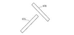
【0080】
この第8の実施の形態では、クロススロット82,85によるスロット給電の例を示したが、図18に示すように、互いに垂直な方向の2本のスロット87A,87Bを離間した位置に配置した所謂ハの字スロットを用いてスロット給電を行ってもよい。
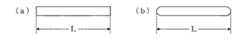
また、クロススロット82,85またはハの字スロットを構成するスロットの平面形状は、図19(a)に示すような矩形であってもよいし、図19(b)に示すような平行二直線の両端を円弧などの曲線でつないだ形状であってもよい。スロットの長さLとは、図19(a)では矩形の長辺の長さであり、図19(b)では対向する二曲線の間隔が最大となる位置の長さである。
なお、図15,図17に示すように、矩形導波管81,84において、クロススロット82、85が形成されている部分と高周波発生器45との間に、マッチング回路44を配置してもよい。これにより、プラズマ負荷からの反射電力を高周波発生器45へ返すことなく再度負荷側へ戻し、効率よくプラズマへ電力供給することができる。
【0081】
以上の本発明の実施の形態で用いるラジアルアンテナ30は、スロット面を構成する導体板31が平板状であるが、図20に示すラジアルアンテナ30Aのように、スロット面を構成する導体板31Aが円錐面状をしていてもよい。円錐面状をしたスロット面から放射(またはリーク)される電磁界は、平板状をした誘電体板13によって規定されるプラズマ面に対して斜め方向から入射されることになる。このため、プラズマによる電磁界の吸収効率が向上するので、アンテナ面とプラズマ面との間に存在する定在波を弱め、プラズマ分布の均一性を向上させることができる。
なお、ラジアルアンテナ30Aのアンテナ面を構成する導体板31Aは、円錐面状以外の凸形状であってもよい。その凸形状は上に凸であっても、下に凸であってもよい。また、キャビティ35の一端面を形成する円形導体部材51Aは、ラジアルアンテナ30Aの導体板31Aにならった凸形状をしていてもよい。
【0082】
【発明の効果】
以上のように本発明によれば、共振器を構成するキャビティを設け、このキャビティに給電される高周波電磁界を回転電磁界に変換すると同時に、この回転電磁界を前記キャビティにおいて共振させながらその一部をラジアル導波路内に供給するので、このキャビティ内で回転電磁界を円偏波とすることによって、前記ラジアル導波路に円偏波になされた回転電磁界を供給することができ、これによって生成されるプラズマの面内分布の均一性を向上させることができる。
【図面の簡単な説明】
【図1】本発明の第1の実施の形態にかかるプラズマ装置を説明する図である。
【図2】本発明の第1の実施の形態にかかるプラズマ装置の給電部を説明する図である。
【図3】本発明の第1の実施の形態にかかるプラズマ装置の給電部における電界分布を説明する図である。
【図4】本発明の第2の実施の形態にかかるプラズマ装置の給電部を説明する図である。
【図5】本発明の第2の実施の形態にかかるプラズマ装置の給電部の作用効果を説明する図である。
【図6】本発明の第2の実施の形態にかかるプラズマ装置の給電部の変形例を説明する図である。
【図7】本発明の第2の実施の形態にかかるプラズマ装置の給電部の変形例を説明する図である。
【図8】本発明の第3の実施の形態にかかるプラズマ装置の給電部を説明する図である。
【図9】本発明の第3の実施の形態にかかるプラズマ装置の給電部の変形例を説明する図である。
【図10】本発明の第3の実施の形態にかかるプラズマ装置の給電部の変形例を説明する図である。
【図11】本発明の第4の実施の形態にかかるプラズマ装置の給電部を説明する図である。
【図12】本発明の第5の実施の形態にかかるプラズマ装置の給電部を説明する図である。
【図13】本発明の第6の実施の形態にかかるプラズマ装置の給電部を説明する図である。
【図14】本発明の第7の実施の形態にかかるプラズマ装置の給電部を説明する図である。
【図15】本発明の第8の実施の形態にかかるプラズマ装置の給電部を説明する図である。
【図16】本発明の第8の実施の形態にかかるプラズマ装置に用いられるクロススロットの設計例を説明する図である。
【図17】本発明の第8の実施の形態にかかるプラズマ装置の給電部の変形例を説明する図である。
【図18】本発明の第8の実施の形態にかかるプラズマ装置に用いられるスロットの他の例を説明する図である。
【図19】スロットの形状を示す平面図である。
【図20】本発明で使用可能なラジアルアンテナの構成例を説明する図である。
【図21】従来のプラズマ装置を説明する図である。
【図22】従来のプラズマ装置における電磁界のモードを説明する図である。
【図23】従来のプラズマ装置におけるプラズマの面内分布を示す模式図である。
【符号の説明】
11…処理容器、12…シールド材、13…誘電体板、14…シール部材、30…ラジアルアンテナ、31,32…導体板、33…ラジアル導波路、34…導体リング、35…キャビティ、36…スロット、41…同軸導波管、41A…外部導体、41B…内部導体、51A…円形導体部材、51B…円筒導体部材、51B’…筒状導体部材、52…給電ピン、53…摂動ピン。[0001]
BACKGROUND OF THE INVENTION
The present invention relates to a plasma apparatus and a plasma generation method for generating plasma by an electromagnetic field supplied into a processing container using a slot antenna.
[0002]
[Prior art]
In the manufacture of semiconductor devices and flat panel displays, plasma devices are frequently used to perform processes such as oxide film formation, semiconductor layer crystal growth, etching, and ashing. Among these plasma devices, there is a high-frequency plasma device that uses a slot antenna to supply a high-frequency electromagnetic field into a processing container and generates high-density plasma by the electromagnetic field. This high-frequency plasma apparatus has a feature that it can stably generate plasma even if the pressure of plasma gas is relatively low.
When performing various processes using such a plasma apparatus, it is necessary to make the two-dimensional plasma distribution (hereinafter referred to as “in-plane distribution”) uniform on the processing surface of a semiconductor substrate or the like.
[0003]
As a method of generating plasma having a uniform in-plane distribution using a slot antenna, a high-frequency electromagnetic field fed from a high-frequency power source is converted into a rotating electromagnetic field, and the rotating high-frequency electromagnetic field made circularly polarized is converted into a slot antenna It is considered to supply.
FIG. 21 is a diagram showing a configuration example of a conventional high-frequency plasma apparatus. FIG. 21 shows a longitudinal sectional structure of a partial configuration of a conventional high-frequency plasma apparatus.
[0004]
A conventional plasma apparatus includes a bottomed
A
The
[0005]
The
[0006]
In the conventional plasma apparatus, the rotating electromagnetic field is supplied to the
That is, the conventional plasma apparatus includes a high-
[0007]
Here, as the circularly
[0008]
A mechanism for supplying a rotating electromagnetic field in the conventional plasma apparatus having such a configuration will be described with reference to FIG. FIG. 22 is a diagram schematically showing an electromagnetic field propagating through the
[0009]
The high-frequency electromagnetic field (FIG. 22A) propagated through the
[0010]
[Problems to be solved by the invention]
However, a part of the rotating electromagnetic field supplied to the
[0011]
As a result, the
By simply supplying the rotating electromagnetic field converted by the
The present invention has been made to solve such problems, and an object thereof is to improve the in-plane uniformity of the plasma distribution.
[0012]
[Means for Solving the Problems]
The plasma apparatus according to the present invention includes:A processing container that accommodates an object to be processed, a radial waveguide formed by opposing first and second conductor plates, and a central portion of the first conductor plate;The high-frequency electromagnetic field that constitutes the resonator and is fed is converted into a rotating electromagnetic field toRadial waveguideSupplying cavityAnd a ring member provided around the opening of the cavity inside the radial waveguide and having the same inner diameter as the inner diameter of the cavity and the second conductor plate, and propagates through the radial waveguide. A slot for supplying the high-frequency electromagnetic field to the processing container.It is characterized by that.
In the present invention, the rotating electromagnetic field resonates in the cavity.Radial waveguideA rotating high-frequency electromagnetic field made circularly polarized is supplied.
Further, by adjusting the thickness and width of the ring member, it is possible to adjust the ratio of the high-frequency electromagnetic field supplied into the radial waveguide among the high-frequency electromagnetic fields resonating in the cavity.
[0014]
As a first configuration example of the plasma device according to the present invention, the cavity isSaidA circular conductor member connected to the outer conductor of the coaxial waveguide that feeds a high-frequency electromagnetic field, and one end connected to the circular conductor member and the other endRadial waveguideAnd a feed pin that is provided at a position spaced from the center of the circular conductor member in the radial direction and connected to one end of the inner conductor of the coaxial waveguide, and the feed pin Circular conductorElementAnd a perturbation pin having one end connected to the circular conductor member at a position that forms a predetermined angle across the center.
In such a configuration, the high-frequency electromagnetic field fed through the coaxial waveguide is converted into a rotating magnetic field by the interaction between the feed pin and the perturbation pin, and resonates in the cavity.Radial waveguideSupplied in.
[0015]
Here, the other end of the power supply pin may be open., SuLot formedSecond conductor plateIt may be connected to.
The other end of the power supply pinSecond conductor plateIs connected to the other end of the power supply pin,Of the second conductor plateA frustoconical conductive member extending to the side may be provided. By using a conductor member with such a shape, the high-frequency electromagnetic field that resonates in the cavity is reduced.Radial waveguideIt can be easily introduced into the inside.
The other end of the perturbation pin may also be open,Second conductor plateIt may be connected to. Moreover, you may be connected to the cylindrical conductor member.
[0016]
Further, the other end of the power supply pin may be connected to the cylindrical conductor member.
In this case, the other end of the perturbation pin, SuLot formedSecond conductor plateOr may be connected to a cylindrical conductor member.
[0017]
As a second configuration example of the plasma device according to the present invention, the cavity isSaidA circular conductor member connected to the outer conductor of the coaxial waveguide that feeds a high-frequency electromagnetic field, and one end connected to the circular conductor member and the other endRadial waveguideAnd a conductive member disposed opposite to the inside of the side wall of the cylindrical conductor member and provided at a position spaced apart from the center of the circular conductor member in the radial direction.SaidIt is characterized by comprising a feed pin connected at one end to the inner conductor of the coaxial waveguide.
In such a configuration, the cavity is formed by the conductive member disposed so as to face the inside of the side wall of the cylindrical conductor member so that the cross sections perpendicular to the axis of the cylindrical conductor member have notch portions facing each other. As a result, the high-frequency electromagnetic field fed through the coaxial waveguide is converted into a rotating electromagnetic field in the cavity and resonates.Radial waveguideSupplied in.
[0018]
Here, the conductive member disposed opposite to the inside of the side wall of the cylindrical conductor member may extend from one end to the other end of the cylindrical conductor member.
The conductive member may have an axial length of the cylindrical conductor member that is approximately ¼ of the wavelength of the high-frequency electromagnetic field. In this case, the length of the parallel portion between the conductive member and the power supply pin is approximately ¼ of the wavelength of the high-frequency electromagnetic field, and a good rotating electromagnetic field can be obtained in the cavity.
In addition, the conductive member isRadial waveguideThe edge part of this side may be shape | molded by the slope shape. By forming in this way, the impedance change between the region where the conductive member is present and the region where the conductive member is not present in the cavity can be moderated, and reflection of the high frequency electromagnetic field at the boundary between the two regions can be suppressed.
When the end portion of the conductive member is formed into a slope shape, the main body excluding the end portion may have an axial length of the cylindrical conductor member that is approximately ¼ of the wavelength of the high-frequency electromagnetic field. Thereby, a favorable rotating electromagnetic field can be obtained in the cavity.
Also, the other end of the feed pin, SuLot formedSecond conductor plateOr may be connected to the conductor member at a position approximately 1/4 of the wavelength of the high-frequency electromagnetic field in the axial direction of the cylindrical conductor member from the circular conductor member.
In addition, as a conductive member provided inside the side wall of the cylindrical conductor member, one or a plurality of sets of cylindrical columnar projections facing each other may be provided in the axial direction.
[0019]
As a third configuration example of the plasma device according to the present invention, the cavity isSaidAn elliptical conductor member connected to the outer conductor of the coaxial waveguide that feeds a high-frequency electromagnetic field, and one end connected to the elliptical conductor member and the other endRadial waveguideAnd a cylindrical conductor member having an elliptical cross section, and spaced apart from the center of the elliptical conductor member in the radial direction and at a predetermined angle with the major axis and minor axis. And a feed pin connected to the inner conductor of the coaxial waveguide.
In such a configuration, a high-frequency electromagnetic field fed through the coaxial waveguide is converted into a rotating electromagnetic field in a cavity having an elliptical cross section, and resonates.Radial waveguideSupplied in.
Where the other end of the feed pin is, SuLot formedSecond conductor plateOr may be connected to the conductor member at a position approximately 1/4 of the wavelength of the high-frequency electromagnetic field in the axial direction of the cylindrical conductor member from the circular conductor member.
[0020]
As a fourth configuration example of the plasma device according to the present invention, the cavity isSaidA circular conductor member connected to the outer conductor of the first and second coaxial waveguides for feeding a high-frequency electromagnetic field, one end connected to the circular conductor member, and the other endRadial waveguideAnd a first power feed pin connected to the inner conductor of the first coaxial waveguide provided at a position radially spaced from the center of the circular conductor member. The first power supply pin and the circular conductorElementAnd a second feed pin connected to the inner conductor of the second coaxial waveguide provided at a predetermined angle with respect to the center of the second coaxial waveguide.
In such a configuration, a rotating electromagnetic field is generated by feeding high-frequency electromagnetic fields having different phases to the first and second feeding pins, and the rotating electromagnetic field resonates in the cavity.Radial waveguideSupplied in.
Here, the other end of each of the first and second power supply pins is, SuLot formedSecond conductor plateOr may be connected to the conductor member at a position approximately 1/4 of the wavelength of the high-frequency electromagnetic field in the axial direction of the cylindrical conductor member from the circular conductor member.
[0021]
As a fifth configuration example of the plasma apparatus according to the present invention, the cavity includes a circular conductor member connected to an outer conductor of at least one coaxial waveguide that feeds a high-frequency electromagnetic field, and one end of the circular conductor member. Connected to the other endRadial waveguideAnd a patch antenna that radiates a high-frequency electromagnetic field fed from at least one coaxial waveguide into the cavity as a rotating electromagnetic field. The patch antenna includes a circular conductor. And a conductive plate connected to the inner conductor of at least one coaxial waveguide disposed opposite to the circular conductor member at a predetermined interval.
In such a configuration, the high frequency electromagnetic field fed through the coaxial waveguide is radiated into the cavity as a rotating electromagnetic field by the patch antenna, and resonates.Radial waveguideSupplied in.
[0022]
Furthermore, as a sixth configuration example of the plasma device according to the present invention, the cavity includes one side or a termination surface of a rectangular waveguide that feeds a high-frequency electromagnetic field, and one end or one end of the rectangular waveguide at one end. Connected to the surface and the other endRadial waveguideA plurality of slots that radiate a high-frequency electromagnetic field into the cavity as a rotating electromagnetic field is formed on one side surface or the end surface of the rectangular waveguide. To do.
In such a configuration, the high-frequency electromagnetic field fed through the rectangular waveguide is radiated into the cavity as a rotating electromagnetic field by a plurality of slots formed on one side surface or the end surface of the rectangular waveguide, While resonatingRadial waveguideSupplied in.
Here, the plurality of slots may be two slots that intersect at the midpoint of each other. A slot constituted by these two slots is called a cross slot.
In addition, the plurality of slots may be two slots that are spaced apart from each other and extend in directions substantially perpendicular to each other. A slot constituted by these two slots is called a C-shaped slot.
[0023]
Further, the plasma generation method according to the present invention is as follows.,BothA high-frequency electromagnetic field is fed to the cavity constituting the vibrator, and the high-frequency electromagnetic field converted into the rotating electromagnetic field is converted into the rotating electromagnetic field while resonating in the cavity.Radial waveguideTo supplyThen, the high-frequency electromagnetic field propagating through the radial waveguide is supplied into a processing container through a slot formed in the radial waveguide, and plasma is generated by the high-frequency electromagnetic field supplied into the processing container. In the plasma generation method, the ring member provided around the opening of the cavity inside the radial waveguide is supplied to the radial waveguide among the high-frequency electromagnetic fields that resonate in the cavity. Adjust the ratio of high frequency electromagnetic fieldIt is characterized by doing.
In this method, while resonating the rotating electromagnetic fieldRadial waveguideBy supplying toRadial waveguideThe high-frequency electromagnetic field supplied to can be a rotating electromagnetic field made circularly polarized.
[0024]
In the first configuration example of the plasma generation method according to the present invention, a feed pin and a perturbation pin are provided in a cavity constituting a resonator, thereby converting a high-frequency electromagnetic field fed through a coaxial waveguide into a rotating electromagnetic field. It converts and resonates in the cavity.
[0025]
The second configuration example of the plasma generation method according to the present invention feeds a high-frequency electromagnetic field to a cavity having notches whose cross sections perpendicular to the propagation direction of the high-frequency electromagnetic field are opposed to each other via a coaxial waveguide. Thus, this is converted into a rotating electromagnetic field and resonated in the cavity.
[0026]
Further, a third configuration example of the plasma generation method according to the present invention supplies a high-frequency electromagnetic field to a cavity having an elliptical cross section perpendicular to the propagation direction of the high-frequency electromagnetic field through a coaxial waveguide. Is converted into a rotating electromagnetic field and resonated in the cavity.
[0027]
In the fourth configuration example of the plasma generation method according to the present invention, high-frequency electromagnetic fields whose phases are different from each other by 90 ° are supplied to the cavities forming the resonator via the first and second coaxial waveguides. Thus, a rotating electromagnetic field is generated and resonated in the cavity.
[0028]
A fifth configuration example of the plasma generation method according to the present invention generates a rotating electromagnetic field in the cavity by feeding a high-frequency electromagnetic field to the patch antenna via a coaxial waveguide.
[0029]
Furthermore, the sixth configuration example of the plasma generation method according to the present invention is configured to cause a high-frequency electromagnetic field fed from a rectangular waveguide to be cavityd from a plurality of slots formed on one side surface or a termination surface of the rectangular waveguide. A rotating electromagnetic field is generated by radiating in.
[0030]
DETAILED DESCRIPTION OF THE INVENTION
Embodiments of the present invention will be described below with reference to the drawings.
1 to 3 are views for explaining a plasma apparatus according to a first embodiment of the present invention.
As shown in FIG. 1A, the plasma apparatus includes a bottomed
[0031]
Inside the
The
[0032]
On the other hand, the
Here, a cross-sectional view taken along line Ib-Ib 'of the plasma apparatus shown in FIG. 1A is shown in FIG. For example, as shown in FIG. 1B, a plurality of
In addition, a power feeding section described later is provided at the center of the
[0033]
As shown in FIG. 1A, the high-frequency electromagnetic field generated by the high-
[0034]
In the present embodiment, the power supply section includes a
[0035]
The
Around the opening of the
Of the electromagnetic field supplied to the
[0036]
With reference to FIG. 2, the configuration of such a power feeding unit will be described in detail.
FIG. 2A is a schematic diagram illustrating the power feeding unit when viewed from the side, and FIG. 2B is a schematic diagram illustrating the arrangement of the power feeding pins 52 and the perturbation pins 53.
In the present embodiment, when a high frequency electromagnetic field of 2.45 GHz is supplied from the
The width c of the
The length l of the
[0037]
When the
[0038]
On the other hand, the
[0039]
The dimensions of the power supply unit shown here are obtained as a result of designing with an emphasis on the reflection coefficient (VS), and it goes without saying that the present invention is not limited to this. For example, when importance is attached to the axial ratio of the rotating electromagnetic field, in FIG. 2, a = about 7.3 cm, d = about 3.5 cm, c = about 2.6 cm, t = about 1.0 cm, l1= L2= About 1.5cm, b1= About 4.3 cm, b2= Φ = 115 ° at a position of about 4.4 cm.
[0040]
Referring to FIG. 3, a mechanism for generating a rotating electromagnetic field by the feeding
If there is no
On the other hand, when the
[0041]
Therefore, in such a plasma apparatus, the high frequency electromagnetic field generated by the
[0042]
At this time, since the rotating electromagnetic field resonates in the
[0043]
In the present embodiment, the other end (tip) of the
[0044]
Next, a second embodiment of the present invention will be described with reference to FIG. In addition, about the member which is common in 1st Embodiment, the same code | symbol is used and the description is abbreviate | omitted.
In the first embodiment described above, the tip of the
The depth d of the
[0045]
The principle of excitation in the
When the tip of the
[0046]
On the other hand, the
By adopting such a configuration, the following effects can be obtained. For example, a high frequency electromagnetic field having a frequency of 2.45 GHz is used, and the length l of the
[0047]
In addition, as shown in FIG. 6A, a
[0048]
As shown in FIG. 6A, the other end of the
Further, the tip of the
Alternatively, the
[0049]
Next, a third embodiment of the present invention will be described with reference to FIG. In addition, about the member which is common in 1st Embodiment, the same code | symbol is used and the description is abbreviate | omitted.
In the first embodiment described above, the
[0050]
As shown in FIG. 8B, the
As a result, in the third embodiment, the
In this embodiment, in order to form the
[0051]
On the other hand, as shown in FIG. 8, the cutout portion of the cross section of the
By providing the
[0052]
In the plasma apparatus having the power supply unit as described above, the high frequency electromagnetic field generated by the
[0053]
At this time, the rotating electromagnetic field resonating in the
[0054]
In the third embodiment, in order to obtain a good rotating electromagnetic field by setting the phase difference between the notch direction component E1 and the direction component E2 orthogonal to the electric field E generated by the
[0055]
Further, as shown in FIG. 10, the ends of the
[0056]
In the third embodiment,
[0057]
Next, a fourth embodiment will be described with reference to FIG.
The plasma device according to the fourth embodiment has an elliptical cross section perpendicular to the central axis of the
Specifically, the
[0058]
In the fourth embodiment, the
As a result, in the electric field E generated by the
[0059]
In the plasma apparatus having such a power feeding unit, the high frequency electromagnetic field fed to the
Therefore, as in the first and third embodiments described above, by converting the high-frequency electromagnetic field into the circularly polarized wave in the
[0060]
By adjusting the depth of the
[0061]
Next, a fifth embodiment will be described with reference to FIG.
The plasma apparatus according to the fifth embodiment feeds power to a
In the present embodiment, as shown in FIG. 12, the first and second power supply pins 52A and 52B connected to the inner conductors of the first and second coaxial waveguides are circular on the
A TE11 mode rotating electromagnetic field is generated in the
In order to give a phase difference of 90 °, a phase conversion circuit may be used, but two coaxial waveguides having different lengths by a quarter of the wavelength of the propagation electromagnetic field are provided with high-frequency electromagnetic waves having the same phase. A field may be supplied.
[0062]
In the plasma apparatus having such a power feeding section, by performing the two-point power feeding as described above, the high-frequency electromagnetic field fed from the two coaxial waveguides is converted into the rotating electromagnetic field, and at the same time, the
Therefore, as in the first to third embodiments described above, by converting a high-frequency electromagnetic field into a circularly polarized wave in the
At this time, by adjusting the depth of the
[0063]
Next, a sixth embodiment will be described with reference to FIG.
The plasma apparatus according to the sixth embodiment generates a rotating electromagnetic field by feeding a patch antenna in a
[0064]
As shown in FIG. 13A, a
[0065]
FIG. 13B is a plan view when the
When the origin O of the coordinate system is set at the center of the
[0066]
The
The length of the
[0067]
A part of the rotating electromagnetic field generated in this way is supplied to the
Therefore, as in the other embodiments described above, a good circularly polarized high-frequency electromagnetic field is radiated (or leaked) from the
At this time, by adjusting the depth of the
[0068]
In order to set the feeding phase difference to the
Further, the planar shape of the
[0069]
Next, a seventh embodiment will be described with reference to FIG. In addition, about the member which is common in 6th Embodiment, the same code | symbol is used and the description is abbreviate | omitted.
The sixth embodiment uses a two-point-
As shown in FIG. 14A, the
[0070]
FIG. 14B is a plan view when the
The
[0071]
The current supplied from the
A part of the rotating electromagnetic field generated in this way is supplied to the
Therefore, as in the sixth embodiment described above, a good circularly polarized high-frequency electromagnetic field is radiated (or leaked) from the
[0072]
The planar shape of the
[0073]
Next, an eighth embodiment will be described with reference to FIG.
The plasma apparatus according to the eighth embodiment generates a rotating electromagnetic field by slot feeding using a TE10 mode
[0074]
A
The lengths of the two slots constituting the
Since the
[0075]
A design example of the
In the cross slot 82A shown in FIG. 16A, the two slots constituting it cross each other at a substantially right angle, and are inclined by about 45 ° with respect to the central axis of the E plane of the
In the
By forming
[0076]
In the eighth embodiment, as shown in FIG. 15, the E surface of the
Note that the center of the
[0077]
In such a plasma apparatus, the high frequency electromagnetic field generated by the
Therefore, as in the other embodiments described above, a good circularly polarized high-frequency electromagnetic field is radiated (or leaked) from the
[0078]
As shown in FIG. 17A, slot feeding may be performed by providing a
[0079]
A design example of the
Therefore, a rotating electromagnetic field can be generated in the
[0080]
In the eighth embodiment, an example of slot power feeding by the
Further, the planar shape of the slots constituting the
As shown in FIGS. 15 and 17, in the
[0081]
In the
The
[0082]
【The invention's effect】
As described above, according to the present invention,,BothA cavity constituting a vibrator is provided, and a high-frequency electromagnetic field fed to the cavity is converted into a rotating electromagnetic field. At the same time, a part of the rotating electromagnetic field is resonated in the cavity.Radial waveguideSince the rotating electromagnetic field is circularly polarized in this cavity,Radial waveguideThus, a rotating electromagnetic field made circularly polarized can be supplied to this, and the uniformity of the in-plane distribution of the plasma generated thereby can be improved.
[Brief description of the drawings]
FIG. 1 is a diagram for explaining a plasma apparatus according to a first embodiment of the present invention.
FIG. 2 is a diagram for explaining a power feeding unit of the plasma apparatus according to the first embodiment of the present invention.
FIG. 3 is a diagram illustrating an electric field distribution in a power feeding unit of the plasma device according to the first embodiment of the present invention.
FIG. 4 is a diagram illustrating a power feeding unit of a plasma device according to a second embodiment of the present invention.
FIG. 5 is a diagram for explaining the operation and effect of a power feeding unit of a plasma apparatus according to a second embodiment of the present invention.
FIG. 6 is a diagram for explaining a modification of the power feeding unit of the plasma device according to the second embodiment of the present invention.
FIG. 7 is a diagram illustrating a modification of the power feeding unit of the plasma device according to the second embodiment of the present invention.
FIG. 8 is a diagram illustrating a power feeding unit of a plasma device according to a third embodiment of the present invention.
FIG. 9 is a diagram illustrating a modification of the power feeding unit of the plasma device according to the third embodiment of the present invention.
FIG. 10 is a diagram for explaining a modification of the power feeding unit of the plasma apparatus according to the third embodiment of the present invention.
FIG. 11 is a diagram illustrating a power feeding unit of a plasma device according to a fourth embodiment of the present invention.
FIG. 12 is a diagram illustrating a power feeding unit of a plasma device according to a fifth embodiment of the present invention.
FIG. 13 is a diagram illustrating a power feeding unit of a plasma device according to a sixth embodiment of the present invention.
FIG. 14 is a diagram illustrating a power feeding unit of a plasma device according to a seventh embodiment of the present invention.
FIG. 15 is a diagram illustrating a power feeding unit of a plasma device according to an eighth embodiment of the present invention.
FIG. 16 is a diagram for explaining a design example of a cross slot used in a plasma apparatus according to an eighth embodiment of the present invention;
FIG. 17 is a diagram illustrating a modification of the power feeding unit of the plasma device according to the eighth embodiment of the present invention.
FIG. 18 is a diagram for explaining another example of a slot used in the plasma apparatus according to the eighth embodiment of the present invention.
FIG. 19 is a plan view showing the shape of a slot.
FIG. 20 is a diagram illustrating a configuration example of a radial antenna that can be used in the present invention.
FIG. 21 is a diagram for explaining a conventional plasma apparatus.
FIG. 22 is a diagram illustrating an electromagnetic field mode in a conventional plasma apparatus.
FIG. 23 is a schematic diagram showing in-plane distribution of plasma in a conventional plasma apparatus.
[Explanation of symbols]
DESCRIPTION OF
Claims (28)
Translated fromJapanese対向する第1および第2の導体板から形成されるラジアル導波路と、
前記第1の導体板の中心部に接続され、共振器を構成するとともに給電される高周波電磁界を回転電磁界に変換して前記ラジアル導波路に供給するキャビティと、
前記ラジアル導波路の内部における前記キャビティの開口部の周囲に設けられ、前記キャビティの内径と同じ内径を有するリング部材と、
前記第2の導体板に形成され、前記ラジアル導波路を伝搬する前記高周波電磁界を前記処理容器に供給するスロットと
を備えることを特徴とするプラズマ装置。A processing container for storing an object to be processed;
A radial waveguide formed from opposing first and second conductor plates;
A cavityconnected to a central portion of the first conductor plate, constituting a resonator and converting a high-frequency electromagnetic field to be fed into a rotating electromagnetic field and supplying the rotary electromagnetic field to theradial waveguide;
A ring member provided around the opening of the cavity inside the radial waveguide and having the same inner diameter as the inner diameter of the cavity;
A slot formed in the second conductor plate and supplying the high-frequency electromagnetic field propagating through the radial waveguide to the processing container;
The plasma apparatuscomprising: a.
前記キャビティは、
前記高周波電磁界を給電する同軸導波管の外部導体と接続された円形導体部材と、
一端がこの円形導体部材と接続され他端が前記ラジアル導波路に開口した円筒導体部材とから形成されるとともに、
前記円形導体部材の中心からその径方向に離間した位置に設けられ前記同軸導波管の内部導体と一端が接続された給電ピンと、
この給電ピンと前記円形導体部材の中心を挟んで所定の角度をなす位置に設けられ一端が前記円形導体部材と接続された摂動ピンと
を備えることを特徴とするプラズマ装置。The plasma apparatus according to claim 1, wherein
The cavity is
A circular conductor member connected to the outer conductor of the coaxial waveguide that feeds the high-frequency electromagnetic field;
A cylindrical conductor member having one end connected to the circular conductor member and the other end opened to the radial waveguide;
A feed pin provided at a position spaced in the radial direction from the center of the circular conductor member and connected to one end of the inner conductor of the coaxial waveguide;
A plasma apparatus, comprising: a power supply pin and a perturbation pin provided at a predetermined angle across the center of the circular conductor member and having one end connected to the circular conductor member .
前記給電ピンの他端は、開放状態になっていることを特徴とするプラズマ装置。The plasma apparatus according to claim2 , wherein
The plasma apparatus according toclaim 1, wherein the other end of the power supply pin is in an open state .
前記給電ピンの他端は、前記第2の導体板に接続されていることを特徴とするプラズマ装置。The plasma apparatus according to claim2 , wherein
The other end of the power supply pin isconnected to the second conductor plate .
前記給電ピンの他端には、前記第2の導体板の側に広がる円錐台状の導電部材が設けられていることを特徴とするプラズマ装置。The plasma apparatus according to claim4 , wherein
A plasma apparatus, whereinthe other endof the power supply pinis provided with afrustoconical conductive member extending towardthe second conductor plate .
前記摂動ピンの他端は、前記第2の導体板に接続されていることを特徴とするプラズマ装置。The plasma apparatus according to claim4 or 5,
The otherend of theperturbationspin, plasma apparatus characterized bybeing connected to saidsecond conductive plate.
前記摂動ピンの他端は、前記円筒導体部材に接続されていることを特徴とするプラズマ装置。The plasma apparatus according to claim4 or5 ,
The other end of the perturbation pin is connected to thecylindrical conductor member .
前記給電ピンの他端は、前記円筒導体部材に接続されていることを特徴とするプラズマ装置。The plasma apparatus according to claim2 , wherein
The other end of the power supply pin is connected to the cylindrical conductor member.
前記摂動ピンの他端は、前記第2の導体板または前記円筒導体部材に接続されていることを特徴とするプラズマ装置。The plasma apparatus according to claim8 , wherein
The other end of theperturbation pin is connected tothe second conductor plate or the cylindrical conductor member.
前記キャビティは、
前記高周波電磁界を給電する同軸導波管の外部導体と接続された円形導体部材と、
一端がこの円形導体部材と接続され他端が前記ラジアル導波路に開口した円筒導体部材と、
この円筒導体部材の側壁内部に対向配置された導電部材とから形成されるとともに、
前記円形導体部材の中心からその径方向に離間した位置に設けられ前記同軸導波管の内部導体と一端が接続された給電ピンを備える
ことを特徴とするプラズマ装置。The plasma apparatus according to claim1 , wherein
Thecavity is
A circular conductor member connected to the outer conductor of the coaxial waveguide that feeds the high-frequency electromagnetic field;
A cylindrical conductor member having one end connected to the circular conductor member and the other end opened to the radial waveguide;
Formed from the conductive member disposed opposite to the inside of the side wall of the cylindrical conductor member,
A plasma apparatus, comprising:a feed pin provided at a position spaced in a radial direction from the center of the circular conductor member and connected to one end of the inner conductor of the coaxial waveguide .
前記導電部材は、前記円筒導体部材の軸方向の長さが前記高周波電磁界の波長の略1/4であることを特徴とするプラズマ装置。The plasma apparatus according to claim10 , wherein
The plasma apparatus, wherein the conductive member has an axial length of the cylindrical conductor member that is approximately ¼ of a wavelength of the high frequency electromagnetic field .
前記導電部材は、前記ラジアル導波路の側の端部が、スロープ状に成形されていることを特徴とするプラズマ装置。In the plasma apparatus of claim 10,
The plasma device according to claim 1, wherein the conductive member hasan end on the radial waveguide side formed into a slope shape .
前記導電部材の前記端部を除く本体は、前記円筒導体部材の軸方向の長さが前記高周波電磁界の波長の略1/4であることを特徴とするプラズマ装置。In the plasma apparatus of claim 12,
Themain body excluding the end of the conductive member has a length in the axial direction of the cylindrical conductor member that is approximately ¼ of the wavelength of the high-frequency electromagnetic field .
前記給電ピンの他端は、前記第2の導体板に接続されていることを特徴とするプラズマ装置。The plasma apparatus according toany one of claims10 to 13,
The other end of the power supply pin is connected to the second conductor plate .
前記給電ピンの他端は、前記円形導体部材から前記円筒導体部材の軸方向に前記高周波電磁界の波長の略1/4離れた位置で前記導体部材に接続されていることを特徴とするプラズマ装置。The plasma apparatus according to claim10 , wherein
The other end of the power supply pin is connected to theconductor member at a position approximately 1/4 of the wavelength of the high-frequency electromagnetic field in the axial direction of the cylindrical conductor member from the circular conductor member. apparatus.
前記キャビティは、
前記高周波電磁界を給電する同軸導波管の外部導体と接続された楕円形導体部材と、
一端がこの楕円形導体部材と接続され他端が前記ラジアル導波路に開口し、断面が楕円形状の筒状導体部材とから形成されるとともに、
前記楕円形導体部材の中心からその径方向に離間しかつその長径および短径と所定の角度をなす位置に設けられ前記同軸導波管の内部導体と接続された給電ピンと
を備えることを特徴とするプラズマ装置。The plasma apparatus according to claim1 , wherein
Thecavity is
An elliptical conductor member connected to an outer conductor of a coaxial waveguide that feeds the high-frequency electromagnetic field;
One end is connected to this elliptical conductor member, the other end is opened to the radial waveguide, and the cross section is formed from an elliptical cylindrical conductor member,
A feeding pin provided at a position spaced apart from the center of the elliptical conductor member in the radial direction and forming a predetermined angle with the major axis and minor axis, and connected to the inner conductor of the coaxial waveguide;
The plasma apparatuscomprising: a.
前記キャビティは、
前記高周波電磁界を給電する第1、第2の同軸導波管の外部導体と接続された円形導体部材と、
一端がこの円形導体部材と接続され他端が前記ラジアル導波路に開口した円筒導体部材とから形成されるとともに、
前記円形導体部材の中心からその径方向に離間した位置に設けられ前記第1の同軸導波管の内部導体と接続された第1の給電ピンと、
この第1の給電ピンと前記円形導体部材の中心を挟んで所定の角度をなす位置に設けられ前記第2の同軸導波管の内部導体と接続された第2の給電ピンと
を備えることを特徴とするプラズマ装置。The plasma apparatus according to claim1, wherein
The cavity is
Afirst, second coaxial waveguidecircular shaped conductor memberconnected to the outer conductor of the feeding ofthe high-frequency electromagnetic field,
One end with is formed from acylindrical conductor member has the other end connected to thecircular-shaped conductive memberThis opened in theradial waveguide,
Afirst feeding pin which is connected from the center of the frontKien shaped conductor member and the inner conductor ofthe first coaxial waveguide provided at aposition spaced in the radialdirection,
A first feed pin and a second feed pin provided at a predetermined angle across the center of the circular conductor member and connected to the inner conductor of the second coaxial waveguide. A plasma apparatus characterized by that.
前記キャビティは、
前記高周波電磁界を給電する少なくとも1本の同軸導波管の外部導体と接続された円形導体部材と、
一端がこの円形導体部材と接続され他端が前記ラジアル導波路に開口した円筒導体部材とから形成されるとともに、
前記少なくとも1本の同軸導波管より給電された前記高周波電磁界を前記回転電磁界として前記キャビティ内に放射するパッチアンテナを備え、
このパッチアンテナは、
前記円形導体部材と、
この円形導体部材と所定の間隔をもって対向配置され前記少なくとも1本の同軸導波管の内部導体と接続された導体板と
を含むことを特徴とするプラズマ装置。The plasma apparatus according to claim1, wherein
The cavity is
A circular conductive member connected to the outer conductor ofat least one coaxialwaveguide for feedingthe high-frequency electromagnetic field,
A cylindrical conductor member having one end connected to the circular conductor member and the other end opened to theradial waveguide ;
A patch antenna that radiates the high-frequency electromagnetic field fed from the at least one coaxial waveguide as the rotating electromagnetic field into the cavity;
This patch antenna
The circular conductor member;
A conductor plate disposed opposite to the circular conductor member at a predetermined interval and connected to an inner conductor of the at least one coaxial waveguide;
A plasma apparatuscomprising:
前記キャビティは、
前記高周波電磁界を給電する矩形導波管の一側面または終端面と、
一端がこの矩形導波管の一側面または終端面と接続され他端が前記ラジアル導波路に開口した円筒導体部材とから形成され、
前記矩形導波管の一側面または終端面には、前記高周波電磁界を前記回転電磁界として前記キャビティ内に放射する複数のスロットが形成されていることを特徴とするプラズマ装置。The plasma apparatus according to claim 1, wherein
The cavity is
Andone side or end face of the rectangular waveguide for feedingthe high-frequency electromagnetic field,
A cylindrical conductor member having one end connected toone side surface or a terminal surface of the rectangular waveguide and the other end opened to theradial waveguide;
A plasma device, wherein a plurality of slots for radiating the high-frequency electromagnetic field into the cavity as the rotating electromagnetic field are formed on one side surface or a terminal surface of the rectangular waveguide .
前記複数のスロットは、互いの中点で交差する2本のスロットであることを特徴とするプラズマ装置。The plasma device according to claim19 , wherein
Theplurality of slots are two slots intersecting each other at a midpoint .
前記複数のスロットは、互いに離間して配置された互いに略垂直な方向にのびる2本のスロットであることを特徴とするプラズマ装置。The plasma device according to claim19 , wherein
Wherein the plurality of slots, a plasma device, characterized in that the two slotsextending in a direction substantially perpendicular to each other which are spaced from each other.
前記ラジアル導波路を伝搬する前記高周波電磁界を前記ラジアル導波路に形成されたスロットを介して処理容器内に供給し、 Supplying the high-frequency electromagnetic field propagating through the radial waveguide into a processing vessel through a slot formed in the radial waveguide;
前記処理容器内に供給された前記高周波電磁界によってプラズマを生成するプラズマ生成方法であって、 A plasma generation method for generating plasma by the high-frequency electromagnetic field supplied into the processing container,
前記ラジアル導波路の内部における前記キャビティの開口部の周囲に設けられたリング部材によって、前記キャビティ内で共振する前記高周波電磁界のうち前記ラジアル導波路に供給される前記高周波電磁界の割合を調整することを特徴とするプラズマ生成方法。 The ratio of the high-frequency electromagnetic field supplied to the radial waveguide out of the high-frequency electromagnetic field resonating in the cavity is adjusted by a ring member provided around the opening of the cavity inside the radial waveguide. And a plasma generation method.
同軸導波管の外部導体と接続された円形導体部材と、一端がこの円形導体部材と接続され他端が前記ラジアル導波路に開口した円筒導体部材とから前記キャビティを形成し、
このキャビティ内に前記同軸導波管の内部導体と接続された給電ピンを前記円形導体部材の中心からその径方向に離間した位置に設けるとともに、
この給電ピンと前記円形導体部材の中心を挟んで所定の角度をなす位置に前記円形導体部材と接続された摂動ピンを設け、
前記同軸導波管を介して前記キャビティに前記高周波電磁界を給電し、
この高周波電磁界を前記給電ピンと前記摂動ピンとによって回転電磁界に変換すると同時に、前記キャビティにおいて共振させながら回転電磁界に変換された前記高周波電磁界を前記ラジアル導波路に供給することを特徴とするプラズマ生成方法。The plasma generation method according to claim 22, wherein
Forming the cavity from a circular conductor member connected to the outer conductor of the coaxial waveguide, and a cylindrical conductor member having one end connected to the circular conductor member and the other end opened to the radial waveguide;
In this cavity, a feed pin connected to the inner conductor of the coaxial waveguide is provided at a position spaced in the radial direction from the center of the circular conductor member, and
A perturbation pin connected to the circular conductor member is provided at a position forming a predetermined angle across the center of the power supply pin and the circular conductor member,
Feeding the high-frequency electromagnetic field to the cavity via the coaxial waveguide;
The high-frequency electromagnetic field is converted into a rotating electromagnetic field by the power feeding pin and the perturbation pin, and at the same time, the high-frequency electromagnetic field converted into the rotating electromagnetic field while being resonated in the cavity is supplied to the radial waveguide. Plasma generation method.
同軸導波管の外部導体と接続された円形導体部材と、一端がこの円形導体部材と接続され他端が前記ラジアル導波路に開口した円筒導体部材と、この円筒導体部材の側壁内部に対向配置された導電部材とから、この円筒導体部材の軸に垂直な断面が互いに対向する1対の切り欠き部を有する前記キャビティを形成し、
このキャビティ内に前記同軸導波管の内部導体と接続された給電ピンを前記円形導体部材の中心からその径方向に離間し、かつ前記キャビティの断面の前記切り欠き部の中心線から離間した位置に設け、
前記同軸導波管を介して前記キャビティに前記高周波電磁界を給電し、
この高周波電磁界を前記給電ピンと前記切り欠き部を有する前記キャビティによって回転電磁界に変換すると同時に、前記キャビティにおいて共振させながら回転電磁界に変換された前記高周波電磁界を前記ラジアル導波路に供給することを特徴とするプラズマ生成方法。In plasma generating method according to claim 22,
A circular conductor member connected to the outer conductor of the coaxial waveguide, a cylindrical conductor member having one end connected to the circular conductor member and the other end opened to theradial waveguide ,and opposed to the inside of the side wall of the cylindrical conductor member And forming the cavityhaving a pair of notches whose cross sections perpendicular to the axis of the cylindrical conductor member face each other ,
In this cavity, the feed pin connected to the inner conductor of the coaxial waveguide is separated from the center of the circular conductor member in the radial direction, and away from the center line of the notch in the cross section of the cavity . In the position,
Through thepre-Symbol coaxial waveguide and feedingthe high-frequency electromagnetic field in said cavity,
And at the same time converted into a rotational electromagnetic field of high-frequency electromagnetic field bysaid cavity with thecutout portion and the feed pin, subjectingsaid high-frequency electromagnetic field which is converted into a rotational electromagnetic field while resonating in the cavity in theradial waveguidefeed plasma generating method comprisingto Rukoto.
同軸導波管の外部導体と接続された楕円形導体部材と、一端がこの楕円形導体部材と接続され他端が前記ラジアル導波路に開口し、断面が楕円形状の筒状導体部材とから前記キャビティを形成し、
このキャビティ内に前記同軸導波管の内部導体と接続された給電ピンを前記楕円形導体部材の中心から離間しかつその長径および短径と所定の角度をなす位置に設け、
前記同軸導波管を介して前記キャビティに前記高周波電磁界を給電し、
この高周波電磁界を前記給電ピンと前記楕円形状の断面を有するキャビティとによって回転電磁界に変換すると同時に、前記キャビティにおいて共振させながら回転電磁界に変換された前記高周波電磁界を前記ラジアル導波路に供給することを特徴とするプラズマ生成方法。In plasma generating method according to claim 22,
Whereinfrom theelliptical circular conductive member connected to the outer conductor of the coaxial waveguide, one end opening the other end is connected to theelliptical circular conductive member in theradial waveguidecross section and thetubular conductor memberelliptical Forming a cavity,
This provided a feeding pin, wherein connected to the inner conductor of the coaxial waveguide into the cavity in a positionthat forms spaced and major axis and minor axis at a predetermined angle fromits center of theelliptical circular conductive member,
Via the coaxial waveguide and feedingthe high-frequency electromagnetic field in said cavity,
And at the same time converted into a rotational electromagnetic field of high-frequency electromagnetic field by a cavity having across section of theelliptical shape and the feed pin, subjectingsaid high-frequency electromagnetic field which is converted into a rotational electromagnetic field while resonating in the cavity in theradial waveguideteapot plasma generating method comprising Rukoto.
第1、第2の同軸導波管の外部導体と接続された円形導体部材と、一端がこの円形導体部材と接続され他端が前記ラジアル導波路に開口した円筒導体部材とから前記キャビティを形成し、
このキャビティ内に前記第1の同軸導波管の内部導体と接続された第1の給電ピンを前記円形導体部材の中心からその径方向に離間した位置に設けるとともに、前記第2の同軸導波管の内部導体と接続された第2の給電ピンを前記第1の給電ピンと前記円形導体部材の中心を挟んで所定の角度をなす位置に設け、
前記第1、第2の同軸導波管を介して前記キャビティに互いに位相が90°異なる高周波電磁界を給電し、
これらの同軸導波管から給電される前記高周波電磁界を回転電磁界に変換すると同時に、前記キャビティにおいて共振させながら回転電磁界に変換された前記高周波電磁界を前記ラジアル導波路に供給することを特徴とするプラズマ生成方法。In plasma generating method according to claim 22,
And afirst, acircular-shaped conductive memberconnected to the outer conductor ofthe second coaxial waveguide,cylindrical conductor member having one end the other end is connected to thecircular-shaped conductive memberThiswas opened to theradial waveguide Forming the cavity,
Provided with afirst feed pin connected to the inner conductor ofthe first coaxial waveguide within the cavity from the center of the frontKien shaped conductor memberat a position spaced in the radial direction, the second coaxial A second power feed pin connected to the inner conductor of the waveguide is provided at a position that forms a predetermined angleacross the center of the first power feed pin and the circular conductor member ;
A high-frequency electromagnetic field having aphase difference of 90 ° is fed to the cavity viathe first and second coaxial waveguides,
At the same time convertingthe high-frequency electromagnetic field which is fed from these coaxial waveguide to the rotating electromagnetic field, thatteapot subjectedthe high-frequency electromagnetic field which is converted into a rotational electromagnetic field while resonating in the cavity in theradial waveguide A plasma generation method characterized by the above.
少なくとも1本の同軸導波管の外部導体と接続された円形導体部材と、一端がこの円形導体部材と接続され他端が前記ラジアル導波路に開口した円筒導体部材とから前記キャビティを形成し、
このキャビティ内に前記少なくとも1本の同軸導波管の内部導体と接続された導体板を前記円形導体部材と所定の間隔をもって対向配置し、前記導体板と前記円形導体部材とを含むパッチアンテナを構成し、
前記少なくとも1本の同軸導波管を介して前記パッチアンテナに前記高周波電磁界を給電して、前記キャビティに回転電磁界を生成し、
前記キャビティにおいて共振させながら回転電磁界に変換された前記高周波電磁界を前記ラジアル導波路に供給することを特徴とするプラズマ生成方法。In plasma generating method according to claim 22,
Forming the cavity from a circular conductor member connected to the outer conductor ofat least one coaxial waveguide and a cylindrical conductor member having one end connected to the circular conductor member and the other end opened to theradial waveguide ;
A patch antenna including aconductor plate connected to the inner conductor of theat least one coaxial waveguide in the cavityfacing the circular conductor member at a predetermined interval, and including the conductor plate and the circular conductor member. Configure
Supplying the high-frequency electromagnetic field to thepatch antenna through theat least one coaxial waveguide, and generating a rotating electromagnetic field in the cavity ;
Plasma generating method comprising Rukototeapot subjectingsaid high-frequency electromagnetic field which is converted into a rotational electromagnetic field while resonating in the cavity in theradial waveguide.
前記高周波電磁界を給電する矩形導波管の一側面または終端面と、一端がこの矩形導波管の一側面または終端面と接続され他端が前記ラジアル導波路に開口した円筒導体部材とから前記キャビティを形成し、
前記矩形導波管より給電された前記高周波電磁界を前記一側面または終端面に形成された複数のスロットより前記キャビティに放射することにより回転電磁界を生成し、
前記キャビティにおいて共振させながら回転電磁界に変換された前記高周波電磁界を前記ラジアル導波路に供給することを特徴とするプラズマ生成方法。In plasma generating method according to claim 22,
One side surface or a termination surface of the rectangular waveguide that feeds the high-frequency electromagnetic field, and a cylindrical conductor member having one end connected toone side surface or the termination surface of the rectangular waveguide and the other end opened to theradial waveguide. Forming the cavity,
A rotating electromagnetic field is generatedby radiating the high-frequency electromagnetic field fed from the rectangular waveguide to the cavity from a plurality of slots formed on the one side surface or the end surface ,
Plasma generating method comprising Rukototeapot subjectingsaid high-frequency electromagnetic field which is converted into a rotational electromagnetic field while resonating in the cavity in theradialwaveguide.
Priority Applications (5)
| Application Number | Priority Date | Filing Date | Title |
|---|---|---|---|
| JP2001247853AJP3625197B2 (en) | 2001-01-18 | 2001-08-17 | Plasma apparatus and plasma generation method |
| PCT/JP2002/000323WO2002058441A1 (en) | 2001-01-18 | 2002-01-18 | Plasma device and plasma generating method |
| KR1020037009440AKR100549678B1 (en) | 2001-01-18 | 2002-01-18 | Plasma Apparatus and Plasma Generating Method |
| US10/466,602US7243610B2 (en) | 2001-01-18 | 2002-01-18 | Plasma device and plasma generating method |
| EP02715809AEP1361782A4 (en) | 2001-01-18 | 2002-01-18 | Plasma device and plasma generating method |
Applications Claiming Priority (3)
| Application Number | Priority Date | Filing Date | Title |
|---|---|---|---|
| JP2001-10291 | 2001-01-18 | ||
| JP2001010291 | 2001-01-18 | ||
| JP2001247853AJP3625197B2 (en) | 2001-01-18 | 2001-08-17 | Plasma apparatus and plasma generation method |
Publications (2)
| Publication Number | Publication Date |
|---|---|
| JP2002289398A JP2002289398A (en) | 2002-10-04 |
| JP3625197B2true JP3625197B2 (en) | 2005-03-02 |
Family
ID=26607895
Family Applications (1)
| Application Number | Title | Priority Date | Filing Date |
|---|---|---|---|
| JP2001247853AExpired - Fee RelatedJP3625197B2 (en) | 2001-01-18 | 2001-08-17 | Plasma apparatus and plasma generation method |
Country Status (5)
| Country | Link |
|---|---|
| US (1) | US7243610B2 (en) |
| EP (1) | EP1361782A4 (en) |
| JP (1) | JP3625197B2 (en) |
| KR (1) | KR100549678B1 (en) |
| WO (1) | WO2002058441A1 (en) |
Families Citing this family (451)
| Publication number | Priority date | Publication date | Assignee | Title |
|---|---|---|---|---|
| JP4504511B2 (en)* | 2000-05-26 | 2010-07-14 | 忠弘 大見 | Plasma processing equipment |
| JP4576291B2 (en)* | 2005-06-06 | 2010-11-04 | 株式会社日立ハイテクノロジーズ | Plasma processing equipment |
| JP5189999B2 (en)* | 2009-01-29 | 2013-04-24 | 東京エレクトロン株式会社 | Microwave plasma processing apparatus and microwave power supply method for microwave plasma processing apparatus |
| US8415884B2 (en) | 2009-09-08 | 2013-04-09 | Tokyo Electron Limited | Stable surface wave plasma source |
| EP3000849B1 (en) | 2010-12-08 | 2018-04-04 | Haydale Graphene Industries PLC | Graphite nanoplatelets, composites comprising them, preparation and uses thereof |
| US20120186747A1 (en)* | 2011-01-26 | 2012-07-26 | Obama Shinji | Plasma processing apparatus |
| JP5913817B2 (en)* | 2011-02-25 | 2016-04-27 | 株式会社日立ハイテクノロジーズ | Plasma processing equipment |
| US20130023129A1 (en) | 2011-07-20 | 2013-01-24 | Asm America, Inc. | Pressure transmitter for a semiconductor processing environment |
| NL2007809C2 (en)* | 2011-11-17 | 2013-05-21 | Draka Comteq Bv | An apparatus for performing a plasma chemical vapour deposition process. |
| US9673533B2 (en)* | 2011-12-29 | 2017-06-06 | Selex Es S.P.A. | Slotted waveguide antenna for near-field focalization of electromagnetic radiation |
| US9155183B2 (en)* | 2012-07-24 | 2015-10-06 | Tokyo Electron Limited | Adjustable slot antenna for control of uniformity in a surface wave plasma source |
| US10714315B2 (en) | 2012-10-12 | 2020-07-14 | Asm Ip Holdings B.V. | Semiconductor reaction chamber showerhead |
| US10009065B2 (en) | 2012-12-05 | 2018-06-26 | At&T Intellectual Property I, L.P. | Backhaul link for distributed antenna system |
| US9113347B2 (en) | 2012-12-05 | 2015-08-18 | At&T Intellectual Property I, Lp | Backhaul link for distributed antenna system |
| US20160376700A1 (en) | 2013-02-01 | 2016-12-29 | Asm Ip Holding B.V. | System for treatment of deposition reactor |
| CN105122951B (en)* | 2013-03-13 | 2018-05-04 | 拉多姆公司 | Use the plasma generator of dielectric resonator |
| US9525524B2 (en) | 2013-05-31 | 2016-12-20 | At&T Intellectual Property I, L.P. | Remote distributed antenna system |
| US9999038B2 (en) | 2013-05-31 | 2018-06-12 | At&T Intellectual Property I, L.P. | Remote distributed antenna system |
| US8897697B1 (en) | 2013-11-06 | 2014-11-25 | At&T Intellectual Property I, Lp | Millimeter-wave surface-wave communications |
| US9209902B2 (en) | 2013-12-10 | 2015-12-08 | At&T Intellectual Property I, L.P. | Quasi-optical coupler |
| US11015245B2 (en) | 2014-03-19 | 2021-05-25 | Asm Ip Holding B.V. | Gas-phase reactor and system having exhaust plenum and components thereof |
| US9880110B2 (en) | 2014-03-26 | 2018-01-30 | Paneratech, Inc. | Material erosion monitoring system and method |
| US9488601B2 (en)* | 2014-03-26 | 2016-11-08 | Paneratech, Inc. | Material erosion monitoring system and method |
| US9692101B2 (en) | 2014-08-26 | 2017-06-27 | At&T Intellectual Property I, L.P. | Guided wave couplers for coupling electromagnetic waves between a waveguide surface and a surface of a wire |
| US9768833B2 (en) | 2014-09-15 | 2017-09-19 | At&T Intellectual Property I, L.P. | Method and apparatus for sensing a condition in a transmission medium of electromagnetic waves |
| US10063280B2 (en) | 2014-09-17 | 2018-08-28 | At&T Intellectual Property I, L.P. | Monitoring and mitigating conditions in a communication network |
| US9628854B2 (en) | 2014-09-29 | 2017-04-18 | At&T Intellectual Property I, L.P. | Method and apparatus for distributing content in a communication network |
| US9615269B2 (en) | 2014-10-02 | 2017-04-04 | At&T Intellectual Property I, L.P. | Method and apparatus that provides fault tolerance in a communication network |
| US9685992B2 (en) | 2014-10-03 | 2017-06-20 | At&T Intellectual Property I, L.P. | Circuit panel network and methods thereof |
| US10941490B2 (en) | 2014-10-07 | 2021-03-09 | Asm Ip Holding B.V. | Multiple temperature range susceptor, assembly, reactor and system including the susceptor, and methods of using the same |
| US9503189B2 (en) | 2014-10-10 | 2016-11-22 | At&T Intellectual Property I, L.P. | Method and apparatus for arranging communication sessions in a communication system |
| US9973299B2 (en) | 2014-10-14 | 2018-05-15 | At&T Intellectual Property I, L.P. | Method and apparatus for adjusting a mode of communication in a communication network |
| US9762289B2 (en) | 2014-10-14 | 2017-09-12 | At&T Intellectual Property I, L.P. | Method and apparatus for transmitting or receiving signals in a transportation system |
| US9577306B2 (en) | 2014-10-21 | 2017-02-21 | At&T Intellectual Property I, L.P. | Guided-wave transmission device and methods for use therewith |
| US9312919B1 (en) | 2014-10-21 | 2016-04-12 | At&T Intellectual Property I, Lp | Transmission device with impairment compensation and methods for use therewith |
| US9520945B2 (en) | 2014-10-21 | 2016-12-13 | At&T Intellectual Property I, L.P. | Apparatus for providing communication services and methods thereof |
| US9653770B2 (en) | 2014-10-21 | 2017-05-16 | At&T Intellectual Property I, L.P. | Guided wave coupler, coupling module and methods for use therewith |
| US9780834B2 (en) | 2014-10-21 | 2017-10-03 | At&T Intellectual Property I, L.P. | Method and apparatus for transmitting electromagnetic waves |
| US9627768B2 (en) | 2014-10-21 | 2017-04-18 | At&T Intellectual Property I, L.P. | Guided-wave transmission device with non-fundamental mode propagation and methods for use therewith |
| US9564947B2 (en) | 2014-10-21 | 2017-02-07 | At&T Intellectual Property I, L.P. | Guided-wave transmission device with diversity and methods for use therewith |
| US9769020B2 (en) | 2014-10-21 | 2017-09-19 | At&T Intellectual Property I, L.P. | Method and apparatus for responding to events affecting communications in a communication network |
| US9544006B2 (en) | 2014-11-20 | 2017-01-10 | At&T Intellectual Property I, L.P. | Transmission device with mode division multiplexing and methods for use therewith |
| US9680670B2 (en) | 2014-11-20 | 2017-06-13 | At&T Intellectual Property I, L.P. | Transmission device with channel equalization and control and methods for use therewith |
| US10009067B2 (en) | 2014-12-04 | 2018-06-26 | At&T Intellectual Property I, L.P. | Method and apparatus for configuring a communication interface |
| US9742462B2 (en) | 2014-12-04 | 2017-08-22 | At&T Intellectual Property I, L.P. | Transmission medium and communication interfaces and methods for use therewith |
| US10340573B2 (en) | 2016-10-26 | 2019-07-02 | At&T Intellectual Property I, L.P. | Launcher with cylindrical coupling device and methods for use therewith |
| US9954287B2 (en) | 2014-11-20 | 2018-04-24 | At&T Intellectual Property I, L.P. | Apparatus for converting wireless signals and electromagnetic waves and methods thereof |
| US9800327B2 (en) | 2014-11-20 | 2017-10-24 | At&T Intellectual Property I, L.P. | Apparatus for controlling operations of a communication device and methods thereof |
| US9654173B2 (en) | 2014-11-20 | 2017-05-16 | At&T Intellectual Property I, L.P. | Apparatus for powering a communication device and methods thereof |
| US9997819B2 (en) | 2015-06-09 | 2018-06-12 | At&T Intellectual Property I, L.P. | Transmission medium and method for facilitating propagation of electromagnetic waves via a core |
| US10243784B2 (en) | 2014-11-20 | 2019-03-26 | At&T Intellectual Property I, L.P. | System for generating topology information and methods thereof |
| US9461706B1 (en) | 2015-07-31 | 2016-10-04 | At&T Intellectual Property I, Lp | Method and apparatus for exchanging communication signals |
| US10144036B2 (en) | 2015-01-30 | 2018-12-04 | At&T Intellectual Property I, L.P. | Method and apparatus for mitigating interference affecting a propagation of electromagnetic waves guided by a transmission medium |
| US9876570B2 (en) | 2015-02-20 | 2018-01-23 | At&T Intellectual Property I, Lp | Guided-wave transmission device with non-fundamental mode propagation and methods for use therewith |
| US10276355B2 (en) | 2015-03-12 | 2019-04-30 | Asm Ip Holding B.V. | Multi-zone reactor, system including the reactor, and method of using the same |
| US9749013B2 (en) | 2015-03-17 | 2017-08-29 | At&T Intellectual Property I, L.P. | Method and apparatus for reducing attenuation of electromagnetic waves guided by a transmission medium |
| US10224981B2 (en) | 2015-04-24 | 2019-03-05 | At&T Intellectual Property I, Lp | Passive electrical coupling device and methods for use therewith |
| US9705561B2 (en) | 2015-04-24 | 2017-07-11 | At&T Intellectual Property I, L.P. | Directional coupling device and methods for use therewith |
| US9793954B2 (en) | 2015-04-28 | 2017-10-17 | At&T Intellectual Property I, L.P. | Magnetic coupling device and methods for use therewith |
| US9948354B2 (en) | 2015-04-28 | 2018-04-17 | At&T Intellectual Property I, L.P. | Magnetic coupling device with reflective plate and methods for use therewith |
| US9871282B2 (en) | 2015-05-14 | 2018-01-16 | At&T Intellectual Property I, L.P. | At least one transmission medium having a dielectric surface that is covered at least in part by a second dielectric |
| US9490869B1 (en) | 2015-05-14 | 2016-11-08 | At&T Intellectual Property I, L.P. | Transmission medium having multiple cores and methods for use therewith |
| US9748626B2 (en) | 2015-05-14 | 2017-08-29 | At&T Intellectual Property I, L.P. | Plurality of cables having different cross-sectional shapes which are bundled together to form a transmission medium |
| US10679767B2 (en) | 2015-05-15 | 2020-06-09 | At&T Intellectual Property I, L.P. | Transmission medium having a conductive material and methods for use therewith |
| US10650940B2 (en) | 2015-05-15 | 2020-05-12 | At&T Intellectual Property I, L.P. | Transmission medium having a conductive material and methods for use therewith |
| US9917341B2 (en) | 2015-05-27 | 2018-03-13 | At&T Intellectual Property I, L.P. | Apparatus and method for launching electromagnetic waves and for modifying radial dimensions of the propagating electromagnetic waves |
| US10154493B2 (en) | 2015-06-03 | 2018-12-11 | At&T Intellectual Property I, L.P. | Network termination and methods for use therewith |
| US10103801B2 (en) | 2015-06-03 | 2018-10-16 | At&T Intellectual Property I, L.P. | Host node device and methods for use therewith |
| US9866309B2 (en) | 2015-06-03 | 2018-01-09 | At&T Intellectual Property I, Lp | Host node device and methods for use therewith |
| US10348391B2 (en) | 2015-06-03 | 2019-07-09 | At&T Intellectual Property I, L.P. | Client node device with frequency conversion and methods for use therewith |
| US10812174B2 (en) | 2015-06-03 | 2020-10-20 | At&T Intellectual Property I, L.P. | Client node device and methods for use therewith |
| US9912381B2 (en) | 2015-06-03 | 2018-03-06 | At&T Intellectual Property I, Lp | Network termination and methods for use therewith |
| US9913139B2 (en) | 2015-06-09 | 2018-03-06 | At&T Intellectual Property I, L.P. | Signal fingerprinting for authentication of communicating devices |
| US10142086B2 (en) | 2015-06-11 | 2018-11-27 | At&T Intellectual Property I, L.P. | Repeater and methods for use therewith |
| US9608692B2 (en) | 2015-06-11 | 2017-03-28 | At&T Intellectual Property I, L.P. | Repeater and methods for use therewith |
| US9820146B2 (en) | 2015-06-12 | 2017-11-14 | At&T Intellectual Property I, L.P. | Method and apparatus for authentication and identity management of communicating devices |
| US9667317B2 (en) | 2015-06-15 | 2017-05-30 | At&T Intellectual Property I, L.P. | Method and apparatus for providing security using network traffic adjustments |
| US9509415B1 (en) | 2015-06-25 | 2016-11-29 | At&T Intellectual Property I, L.P. | Methods and apparatus for inducing a fundamental wave mode on a transmission medium |
| US9640850B2 (en) | 2015-06-25 | 2017-05-02 | At&T Intellectual Property I, L.P. | Methods and apparatus for inducing a non-fundamental wave mode on a transmission medium |
| US9865911B2 (en) | 2015-06-25 | 2018-01-09 | At&T Intellectual Property I, L.P. | Waveguide system for slot radiating first electromagnetic waves that are combined into a non-fundamental wave mode second electromagnetic wave on a transmission medium |
| US10458018B2 (en) | 2015-06-26 | 2019-10-29 | Asm Ip Holding B.V. | Structures including metal carbide material, devices including the structures, and methods of forming same |
| US9722318B2 (en) | 2015-07-14 | 2017-08-01 | At&T Intellectual Property I, L.P. | Method and apparatus for coupling an antenna to a device |
| US10033108B2 (en) | 2015-07-14 | 2018-07-24 | At&T Intellectual Property I, L.P. | Apparatus and methods for generating an electromagnetic wave having a wave mode that mitigates interference |
| US10320586B2 (en) | 2015-07-14 | 2019-06-11 | At&T Intellectual Property I, L.P. | Apparatus and methods for generating non-interfering electromagnetic waves on an insulated transmission medium |
| US9628116B2 (en) | 2015-07-14 | 2017-04-18 | At&T Intellectual Property I, L.P. | Apparatus and methods for transmitting wireless signals |
| US10341142B2 (en) | 2015-07-14 | 2019-07-02 | At&T Intellectual Property I, L.P. | Apparatus and methods for generating non-interfering electromagnetic waves on an uninsulated conductor |
| US9882257B2 (en) | 2015-07-14 | 2018-01-30 | At&T Intellectual Property I, L.P. | Method and apparatus for launching a wave mode that mitigates interference |
| US9853342B2 (en) | 2015-07-14 | 2017-12-26 | At&T Intellectual Property I, L.P. | Dielectric transmission medium connector and methods for use therewith |
| US10033107B2 (en) | 2015-07-14 | 2018-07-24 | At&T Intellectual Property I, L.P. | Method and apparatus for coupling an antenna to a device |
| US10205655B2 (en) | 2015-07-14 | 2019-02-12 | At&T Intellectual Property I, L.P. | Apparatus and methods for communicating utilizing an antenna array and multiple communication paths |
| US10170840B2 (en) | 2015-07-14 | 2019-01-01 | At&T Intellectual Property I, L.P. | Apparatus and methods for sending or receiving electromagnetic signals |
| US10148016B2 (en) | 2015-07-14 | 2018-12-04 | At&T Intellectual Property I, L.P. | Apparatus and methods for communicating utilizing an antenna array |
| US9847566B2 (en) | 2015-07-14 | 2017-12-19 | At&T Intellectual Property I, L.P. | Method and apparatus for adjusting a field of a signal to mitigate interference |
| US9836957B2 (en) | 2015-07-14 | 2017-12-05 | At&T Intellectual Property I, L.P. | Method and apparatus for communicating with premises equipment |
| US10044409B2 (en) | 2015-07-14 | 2018-08-07 | At&T Intellectual Property I, L.P. | Transmission medium and methods for use therewith |
| US9608740B2 (en) | 2015-07-15 | 2017-03-28 | At&T Intellectual Property I, L.P. | Method and apparatus for launching a wave mode that mitigates interference |
| US10090606B2 (en) | 2015-07-15 | 2018-10-02 | At&T Intellectual Property I, L.P. | Antenna system with dielectric array and methods for use therewith |
| US9793951B2 (en) | 2015-07-15 | 2017-10-17 | At&T Intellectual Property I, L.P. | Method and apparatus for launching a wave mode that mitigates interference |
| US9912027B2 (en) | 2015-07-23 | 2018-03-06 | At&T Intellectual Property I, L.P. | Method and apparatus for exchanging communication signals |
| US10784670B2 (en) | 2015-07-23 | 2020-09-22 | At&T Intellectual Property I, L.P. | Antenna support for aligning an antenna |
| US9749053B2 (en) | 2015-07-23 | 2017-08-29 | At&T Intellectual Property I, L.P. | Node device, repeater and methods for use therewith |
| US9871283B2 (en) | 2015-07-23 | 2018-01-16 | At&T Intellectual Property I, Lp | Transmission medium having a dielectric core comprised of plural members connected by a ball and socket configuration |
| US9948333B2 (en) | 2015-07-23 | 2018-04-17 | At&T Intellectual Property I, L.P. | Method and apparatus for wireless communications to mitigate interference |
| US10020587B2 (en) | 2015-07-31 | 2018-07-10 | At&T Intellectual Property I, L.P. | Radial antenna and methods for use therewith |
| US9735833B2 (en) | 2015-07-31 | 2017-08-15 | At&T Intellectual Property I, L.P. | Method and apparatus for communications management in a neighborhood network |
| US9967173B2 (en) | 2015-07-31 | 2018-05-08 | At&T Intellectual Property I, L.P. | Method and apparatus for authentication and identity management of communicating devices |
| US9904535B2 (en) | 2015-09-14 | 2018-02-27 | At&T Intellectual Property I, L.P. | Method and apparatus for distributing software |
| US10136434B2 (en) | 2015-09-16 | 2018-11-20 | At&T Intellectual Property I, L.P. | Method and apparatus for use with a radio distributed antenna system having an ultra-wideband control channel |
| US10051629B2 (en) | 2015-09-16 | 2018-08-14 | At&T Intellectual Property I, L.P. | Method and apparatus for use with a radio distributed antenna system having an in-band reference signal |
| US10009063B2 (en) | 2015-09-16 | 2018-06-26 | At&T Intellectual Property I, L.P. | Method and apparatus for use with a radio distributed antenna system having an out-of-band reference signal |
| US10009901B2 (en) | 2015-09-16 | 2018-06-26 | At&T Intellectual Property I, L.P. | Method, apparatus, and computer-readable storage medium for managing utilization of wireless resources between base stations |
| US10079661B2 (en) | 2015-09-16 | 2018-09-18 | At&T Intellectual Property I, L.P. | Method and apparatus for use with a radio distributed antenna system having a clock reference |
| US9705571B2 (en) | 2015-09-16 | 2017-07-11 | At&T Intellectual Property I, L.P. | Method and apparatus for use with a radio distributed antenna system |
| US9769128B2 (en) | 2015-09-28 | 2017-09-19 | At&T Intellectual Property I, L.P. | Method and apparatus for encryption of communications over a network |
| US9729197B2 (en) | 2015-10-01 | 2017-08-08 | At&T Intellectual Property I, L.P. | Method and apparatus for communicating network management traffic over a network |
| US9882277B2 (en) | 2015-10-02 | 2018-01-30 | At&T Intellectual Property I, Lp | Communication device and antenna assembly with actuated gimbal mount |
| US9876264B2 (en) | 2015-10-02 | 2018-01-23 | At&T Intellectual Property I, Lp | Communication system, guided wave switch and methods for use therewith |
| US10074890B2 (en) | 2015-10-02 | 2018-09-11 | At&T Intellectual Property I, L.P. | Communication device and antenna with integrated light assembly |
| US10665942B2 (en) | 2015-10-16 | 2020-05-26 | At&T Intellectual Property I, L.P. | Method and apparatus for adjusting wireless communications |
| US10355367B2 (en) | 2015-10-16 | 2019-07-16 | At&T Intellectual Property I, L.P. | Antenna structure for exchanging wireless signals |
| US10051483B2 (en) | 2015-10-16 | 2018-08-14 | At&T Intellectual Property I, L.P. | Method and apparatus for directing wireless signals |
| US10211308B2 (en) | 2015-10-21 | 2019-02-19 | Asm Ip Holding B.V. | NbMC layers |
| US11139308B2 (en) | 2015-12-29 | 2021-10-05 | Asm Ip Holding B.V. | Atomic layer deposition of III-V compounds to form V-NAND devices |
| US10529554B2 (en) | 2016-02-19 | 2020-01-07 | Asm Ip Holding B.V. | Method for forming silicon nitride film selectively on sidewalls or flat surfaces of trenches |
| US10343920B2 (en) | 2016-03-18 | 2019-07-09 | Asm Ip Holding B.V. | Aligned carbon nanotubes |
| NL2017575B1 (en) | 2016-10-04 | 2018-04-13 | Draka Comteq Bv | A method and an apparatus for performing a plasma chemical vapour deposition process and a method |
| US10367080B2 (en) | 2016-05-02 | 2019-07-30 | Asm Ip Holding B.V. | Method of forming a germanium oxynitride film |
| US11453943B2 (en) | 2016-05-25 | 2022-09-27 | Asm Ip Holding B.V. | Method for forming carbon-containing silicon/metal oxide or nitride film by ALD using silicon precursor and hydrocarbon precursor |
| US10612137B2 (en) | 2016-07-08 | 2020-04-07 | Asm Ip Holdings B.V. | Organic reactants for atomic layer deposition |
| US9859151B1 (en) | 2016-07-08 | 2018-01-02 | Asm Ip Holding B.V. | Selective film deposition method to form air gaps |
| US9887082B1 (en) | 2016-07-28 | 2018-02-06 | Asm Ip Holding B.V. | Method and apparatus for filling a gap |
| KR102532607B1 (en) | 2016-07-28 | 2023-05-15 | 에이에스엠 아이피 홀딩 비.브이. | Substrate processing apparatus and method of operating the same |
| US9812320B1 (en) | 2016-07-28 | 2017-11-07 | Asm Ip Holding B.V. | Method and apparatus for filling a gap |
| US9912419B1 (en) | 2016-08-24 | 2018-03-06 | At&T Intellectual Property I, L.P. | Method and apparatus for managing a fault in a distributed antenna system |
| US9860075B1 (en) | 2016-08-26 | 2018-01-02 | At&T Intellectual Property I, L.P. | Method and communication node for broadband distribution |
| US10291311B2 (en) | 2016-09-09 | 2019-05-14 | At&T Intellectual Property I, L.P. | Method and apparatus for mitigating a fault in a distributed antenna system |
| US11032819B2 (en) | 2016-09-15 | 2021-06-08 | At&T Intellectual Property I, L.P. | Method and apparatus for use with a radio distributed antenna system having a control channel reference signal |
| US10340600B2 (en) | 2016-10-18 | 2019-07-02 | At&T Intellectual Property I, L.P. | Apparatus and methods for launching guided waves via plural waveguide systems |
| US10135147B2 (en) | 2016-10-18 | 2018-11-20 | At&T Intellectual Property I, L.P. | Apparatus and methods for launching guided waves via an antenna |
| US10135146B2 (en) | 2016-10-18 | 2018-11-20 | At&T Intellectual Property I, L.P. | Apparatus and methods for launching guided waves via circuits |
| US9991580B2 (en) | 2016-10-21 | 2018-06-05 | At&T Intellectual Property I, L.P. | Launcher and coupling system for guided wave mode cancellation |
| US10374316B2 (en) | 2016-10-21 | 2019-08-06 | At&T Intellectual Property I, L.P. | System and dielectric antenna with non-uniform dielectric |
| US10811767B2 (en) | 2016-10-21 | 2020-10-20 | At&T Intellectual Property I, L.P. | System and dielectric antenna with convex dielectric radome |
| US9876605B1 (en) | 2016-10-21 | 2018-01-23 | At&T Intellectual Property I, L.P. | Launcher and coupling system to support desired guided wave mode |
| US10312567B2 (en) | 2016-10-26 | 2019-06-04 | At&T Intellectual Property I, L.P. | Launcher with planar strip antenna and methods for use therewith |
| US11532757B2 (en) | 2016-10-27 | 2022-12-20 | Asm Ip Holding B.V. | Deposition of charge trapping layers |
| US10714350B2 (en) | 2016-11-01 | 2020-07-14 | ASM IP Holdings, B.V. | Methods for forming a transition metal niobium nitride film on a substrate by atomic layer deposition and related semiconductor device structures |
| US10225025B2 (en) | 2016-11-03 | 2019-03-05 | At&T Intellectual Property I, L.P. | Method and apparatus for detecting a fault in a communication system |
| US10498044B2 (en) | 2016-11-03 | 2019-12-03 | At&T Intellectual Property I, L.P. | Apparatus for configuring a surface of an antenna |
| US10224634B2 (en) | 2016-11-03 | 2019-03-05 | At&T Intellectual Property I, L.P. | Methods and apparatus for adjusting an operational characteristic of an antenna |
| US10291334B2 (en) | 2016-11-03 | 2019-05-14 | At&T Intellectual Property I, L.P. | System for detecting a fault in a communication system |
| KR102546317B1 (en) | 2016-11-15 | 2023-06-21 | 에이에스엠 아이피 홀딩 비.브이. | Gas supply unit and substrate processing apparatus including the same |
| US10535928B2 (en) | 2016-11-23 | 2020-01-14 | At&T Intellectual Property I, L.P. | Antenna system and methods for use therewith |
| US10340601B2 (en) | 2016-11-23 | 2019-07-02 | At&T Intellectual Property I, L.P. | Multi-antenna system and methods for use therewith |
| US10340603B2 (en) | 2016-11-23 | 2019-07-02 | At&T Intellectual Property I, L.P. | Antenna system having shielded structural configurations for assembly |
| US10178445B2 (en) | 2016-11-23 | 2019-01-08 | At&T Intellectual Property I, L.P. | Methods, devices, and systems for load balancing between a plurality of waveguides |
| US10090594B2 (en) | 2016-11-23 | 2018-10-02 | At&T Intellectual Property I, L.P. | Antenna system having structural configurations for assembly |
| US10305190B2 (en) | 2016-12-01 | 2019-05-28 | At&T Intellectual Property I, L.P. | Reflecting dielectric antenna system and methods for use therewith |
| US10361489B2 (en) | 2016-12-01 | 2019-07-23 | At&T Intellectual Property I, L.P. | Dielectric dish antenna system and methods for use therewith |
| US9927517B1 (en) | 2016-12-06 | 2018-03-27 | At&T Intellectual Property I, L.P. | Apparatus and methods for sensing rainfall |
| US10755542B2 (en) | 2016-12-06 | 2020-08-25 | At&T Intellectual Property I, L.P. | Method and apparatus for surveillance via guided wave communication |
| US10439675B2 (en) | 2016-12-06 | 2019-10-08 | At&T Intellectual Property I, L.P. | Method and apparatus for repeating guided wave communication signals |
| US10637149B2 (en) | 2016-12-06 | 2020-04-28 | At&T Intellectual Property I, L.P. | Injection molded dielectric antenna and methods for use therewith |
| US10694379B2 (en) | 2016-12-06 | 2020-06-23 | At&T Intellectual Property I, L.P. | Waveguide system with device-based authentication and methods for use therewith |
| US10819035B2 (en) | 2016-12-06 | 2020-10-27 | At&T Intellectual Property I, L.P. | Launcher with helical antenna and methods for use therewith |
| US10326494B2 (en) | 2016-12-06 | 2019-06-18 | At&T Intellectual Property I, L.P. | Apparatus for measurement de-embedding and methods for use therewith |
| US10135145B2 (en) | 2016-12-06 | 2018-11-20 | At&T Intellectual Property I, L.P. | Apparatus and methods for generating an electromagnetic wave along a transmission medium |
| US10020844B2 (en) | 2016-12-06 | 2018-07-10 | T&T Intellectual Property I, L.P. | Method and apparatus for broadcast communication via guided waves |
| US10382976B2 (en) | 2016-12-06 | 2019-08-13 | At&T Intellectual Property I, L.P. | Method and apparatus for managing wireless communications based on communication paths and network device positions |
| US10727599B2 (en) | 2016-12-06 | 2020-07-28 | At&T Intellectual Property I, L.P. | Launcher with slot antenna and methods for use therewith |
| US10168695B2 (en) | 2016-12-07 | 2019-01-01 | At&T Intellectual Property I, L.P. | Method and apparatus for controlling an unmanned aircraft |
| US9893795B1 (en) | 2016-12-07 | 2018-02-13 | At&T Intellectual Property I, Lp | Method and repeater for broadband distribution |
| US10446936B2 (en) | 2016-12-07 | 2019-10-15 | At&T Intellectual Property I, L.P. | Multi-feed dielectric antenna system and methods for use therewith |
| US10027397B2 (en) | 2016-12-07 | 2018-07-17 | At&T Intellectual Property I, L.P. | Distributed antenna system and methods for use therewith |
| US10389029B2 (en) | 2016-12-07 | 2019-08-20 | At&T Intellectual Property I, L.P. | Multi-feed dielectric antenna system with core selection and methods for use therewith |
| US10243270B2 (en) | 2016-12-07 | 2019-03-26 | At&T Intellectual Property I, L.P. | Beam adaptive multi-feed dielectric antenna system and methods for use therewith |
| US10359749B2 (en) | 2016-12-07 | 2019-07-23 | At&T Intellectual Property I, L.P. | Method and apparatus for utilities management via guided wave communication |
| US10139820B2 (en) | 2016-12-07 | 2018-11-27 | At&T Intellectual Property I, L.P. | Method and apparatus for deploying equipment of a communication system |
| US10547348B2 (en) | 2016-12-07 | 2020-01-28 | At&T Intellectual Property I, L.P. | Method and apparatus for switching transmission mediums in a communication system |
| US9998870B1 (en) | 2016-12-08 | 2018-06-12 | At&T Intellectual Property I, L.P. | Method and apparatus for proximity sensing |
| US10938108B2 (en) | 2016-12-08 | 2021-03-02 | At&T Intellectual Property I, L.P. | Frequency selective multi-feed dielectric antenna system and methods for use therewith |
| US9911020B1 (en) | 2016-12-08 | 2018-03-06 | At&T Intellectual Property I, L.P. | Method and apparatus for tracking via a radio frequency identification device |
| US10601494B2 (en) | 2016-12-08 | 2020-03-24 | At&T Intellectual Property I, L.P. | Dual-band communication device and method for use therewith |
| US10103422B2 (en) | 2016-12-08 | 2018-10-16 | At&T Intellectual Property I, L.P. | Method and apparatus for mounting network devices |
| US10069535B2 (en) | 2016-12-08 | 2018-09-04 | At&T Intellectual Property I, L.P. | Apparatus and methods for launching electromagnetic waves having a certain electric field structure |
| US10411356B2 (en) | 2016-12-08 | 2019-09-10 | At&T Intellectual Property I, L.P. | Apparatus and methods for selectively targeting communication devices with an antenna array |
| US10530505B2 (en) | 2016-12-08 | 2020-01-07 | At&T Intellectual Property I, L.P. | Apparatus and methods for launching electromagnetic waves along a transmission medium |
| US10389037B2 (en) | 2016-12-08 | 2019-08-20 | At&T Intellectual Property I, L.P. | Apparatus and methods for selecting sections of an antenna array and use therewith |
| US10777873B2 (en) | 2016-12-08 | 2020-09-15 | At&T Intellectual Property I, L.P. | Method and apparatus for mounting network devices |
| US10326689B2 (en) | 2016-12-08 | 2019-06-18 | At&T Intellectual Property I, L.P. | Method and system for providing alternative communication paths |
| US10916969B2 (en) | 2016-12-08 | 2021-02-09 | At&T Intellectual Property I, L.P. | Method and apparatus for providing power using an inductive coupling |
| US10264586B2 (en) | 2016-12-09 | 2019-04-16 | At&T Mobility Ii Llc | Cloud-based packet controller and methods for use therewith |
| US10340983B2 (en) | 2016-12-09 | 2019-07-02 | At&T Intellectual Property I, L.P. | Method and apparatus for surveying remote sites via guided wave communications |
| US9838896B1 (en) | 2016-12-09 | 2017-12-05 | At&T Intellectual Property I, L.P. | Method and apparatus for assessing network coverage |
| KR102762543B1 (en)* | 2016-12-14 | 2025-02-05 | 에이에스엠 아이피 홀딩 비.브이. | Substrate processing apparatus |
| US11581186B2 (en) | 2016-12-15 | 2023-02-14 | Asm Ip Holding B.V. | Sequential infiltration synthesis apparatus |
| US11447861B2 (en) | 2016-12-15 | 2022-09-20 | Asm Ip Holding B.V. | Sequential infiltration synthesis apparatus and a method of forming a patterned structure |
| KR102700194B1 (en) | 2016-12-19 | 2024-08-28 | 에이에스엠 아이피 홀딩 비.브이. | Substrate processing apparatus |
| US10269558B2 (en) | 2016-12-22 | 2019-04-23 | Asm Ip Holding B.V. | Method of forming a structure on a substrate |
| US11390950B2 (en) | 2017-01-10 | 2022-07-19 | Asm Ip Holding B.V. | Reactor system and method to reduce residue buildup during a film deposition process |
| US10468261B2 (en) | 2017-02-15 | 2019-11-05 | Asm Ip Holding B.V. | Methods for forming a metallic film on a substrate by cyclical deposition and related semiconductor device structures |
| US9973940B1 (en) | 2017-02-27 | 2018-05-15 | At&T Intellectual Property I, L.P. | Apparatus and methods for dynamic impedance matching of a guided wave launcher |
| US10298293B2 (en) | 2017-03-13 | 2019-05-21 | At&T Intellectual Property I, L.P. | Apparatus of communication utilizing wireless network devices |
| US10529563B2 (en) | 2017-03-29 | 2020-01-07 | Asm Ip Holdings B.V. | Method for forming doped metal oxide films on a substrate by cyclical deposition and related semiconductor device structures |
| US10770286B2 (en) | 2017-05-08 | 2020-09-08 | Asm Ip Holdings B.V. | Methods for selectively forming a silicon nitride film on a substrate and related semiconductor device structures |
| US12040200B2 (en) | 2017-06-20 | 2024-07-16 | Asm Ip Holding B.V. | Semiconductor processing apparatus and methods for calibrating a semiconductor processing apparatus |
| US11306395B2 (en) | 2017-06-28 | 2022-04-19 | Asm Ip Holding B.V. | Methods for depositing a transition metal nitride film on a substrate by atomic layer deposition and related deposition apparatus |
| KR20190009245A (en) | 2017-07-18 | 2019-01-28 | 에이에스엠 아이피 홀딩 비.브이. | Methods for forming a semiconductor device structure and related semiconductor device structures |
| US11374112B2 (en) | 2017-07-19 | 2022-06-28 | Asm Ip Holding B.V. | Method for depositing a group IV semiconductor and related semiconductor device structures |
| US10541333B2 (en) | 2017-07-19 | 2020-01-21 | Asm Ip Holding B.V. | Method for depositing a group IV semiconductor and related semiconductor device structures |
| US11018002B2 (en) | 2017-07-19 | 2021-05-25 | Asm Ip Holding B.V. | Method for selectively depositing a Group IV semiconductor and related semiconductor device structures |
| US10590535B2 (en) | 2017-07-26 | 2020-03-17 | Asm Ip Holdings B.V. | Chemical treatment, deposition and/or infiltration apparatus and method for using the same |
| JP6925903B2 (en)* | 2017-08-02 | 2021-08-25 | 矢崎総業株式会社 | antenna |
| TWI815813B (en) | 2017-08-04 | 2023-09-21 | 荷蘭商Asm智慧財產控股公司 | Showerhead assembly for distributing a gas within a reaction chamber |
| US10770336B2 (en) | 2017-08-08 | 2020-09-08 | Asm Ip Holding B.V. | Substrate lift mechanism and reactor including same |
| US10692741B2 (en) | 2017-08-08 | 2020-06-23 | Asm Ip Holdings B.V. | Radiation shield |
| US11139191B2 (en) | 2017-08-09 | 2021-10-05 | Asm Ip Holding B.V. | Storage apparatus for storing cassettes for substrates and processing apparatus equipped therewith |
| US11769682B2 (en) | 2017-08-09 | 2023-09-26 | Asm Ip Holding B.V. | Storage apparatus for storing cassettes for substrates and processing apparatus equipped therewith |
| US11830730B2 (en) | 2017-08-29 | 2023-11-28 | Asm Ip Holding B.V. | Layer forming method and apparatus |
| US11056344B2 (en) | 2017-08-30 | 2021-07-06 | Asm Ip Holding B.V. | Layer forming method |
| US11295980B2 (en) | 2017-08-30 | 2022-04-05 | Asm Ip Holding B.V. | Methods for depositing a molybdenum metal film over a dielectric surface of a substrate by a cyclical deposition process and related semiconductor device structures |
| KR102491945B1 (en) | 2017-08-30 | 2023-01-26 | 에이에스엠 아이피 홀딩 비.브이. | Substrate processing apparatus |
| US10658205B2 (en) | 2017-09-28 | 2020-05-19 | Asm Ip Holdings B.V. | Chemical dispensing apparatus and methods for dispensing a chemical to a reaction chamber |
| US10403504B2 (en) | 2017-10-05 | 2019-09-03 | Asm Ip Holding B.V. | Method for selectively depositing a metallic film on a substrate |
| US10923344B2 (en) | 2017-10-30 | 2021-02-16 | Asm Ip Holding B.V. | Methods for forming a semiconductor structure and related semiconductor structures |
| US11022879B2 (en) | 2017-11-24 | 2021-06-01 | Asm Ip Holding B.V. | Method of forming an enhanced unexposed photoresist layer |
| US11639811B2 (en) | 2017-11-27 | 2023-05-02 | Asm Ip Holding B.V. | Apparatus including a clean mini environment |
| JP7214724B2 (en) | 2017-11-27 | 2023-01-30 | エーエスエム アイピー ホールディング ビー.ブイ. | Storage device for storing wafer cassettes used in batch furnaces |
| US10872771B2 (en) | 2018-01-16 | 2020-12-22 | Asm Ip Holding B. V. | Method for depositing a material film on a substrate within a reaction chamber by a cyclical deposition process and related device structures |
| TWI799494B (en) | 2018-01-19 | 2023-04-21 | 荷蘭商Asm 智慧財產控股公司 | Deposition method |
| US11482412B2 (en) | 2018-01-19 | 2022-10-25 | Asm Ip Holding B.V. | Method for depositing a gap-fill layer by plasma-assisted deposition |
| US11081345B2 (en) | 2018-02-06 | 2021-08-03 | Asm Ip Holding B.V. | Method of post-deposition treatment for silicon oxide film |
| KR102657269B1 (en) | 2018-02-14 | 2024-04-16 | 에이에스엠 아이피 홀딩 비.브이. | Method for depositing a ruthenium-containing film on a substrate by a cyclic deposition process |
| US10896820B2 (en) | 2018-02-14 | 2021-01-19 | Asm Ip Holding B.V. | Method for depositing a ruthenium-containing film on a substrate by a cyclical deposition process |
| US10731249B2 (en) | 2018-02-15 | 2020-08-04 | Asm Ip Holding B.V. | Method of forming a transition metal containing film on a substrate by a cyclical deposition process, a method for supplying a transition metal halide compound to a reaction chamber, and related vapor deposition apparatus |
| KR102636427B1 (en) | 2018-02-20 | 2024-02-13 | 에이에스엠 아이피 홀딩 비.브이. | Substrate processing method and apparatus |
| US10975470B2 (en) | 2018-02-23 | 2021-04-13 | Asm Ip Holding B.V. | Apparatus for detecting or monitoring for a chemical precursor in a high temperature environment |
| US11473195B2 (en) | 2018-03-01 | 2022-10-18 | Asm Ip Holding B.V. | Semiconductor processing apparatus and a method for processing a substrate |
| US11629406B2 (en) | 2018-03-09 | 2023-04-18 | Asm Ip Holding B.V. | Semiconductor processing apparatus comprising one or more pyrometers for measuring a temperature of a substrate during transfer of the substrate |
| US11114283B2 (en) | 2018-03-16 | 2021-09-07 | Asm Ip Holding B.V. | Reactor, system including the reactor, and methods of manufacturing and using same |
| KR102646467B1 (en) | 2018-03-27 | 2024-03-11 | 에이에스엠 아이피 홀딩 비.브이. | Method of forming an electrode on a substrate and a semiconductor device structure including an electrode |
| US11230766B2 (en) | 2018-03-29 | 2022-01-25 | Asm Ip Holding B.V. | Substrate processing apparatus and method |
| US11088002B2 (en) | 2018-03-29 | 2021-08-10 | Asm Ip Holding B.V. | Substrate rack and a substrate processing system and method |
| KR102600229B1 (en) | 2018-04-09 | 2023-11-10 | 에이에스엠 아이피 홀딩 비.브이. | Substrate supporting device, substrate processing apparatus including the same and substrate processing method |
| TWI843623B (en) | 2018-05-08 | 2024-05-21 | 荷蘭商Asm Ip私人控股有限公司 | Methods for depositing an oxide film on a substrate by a cyclical deposition process and related device structures |
| US12025484B2 (en) | 2018-05-08 | 2024-07-02 | Asm Ip Holding B.V. | Thin film forming method |
| US12272527B2 (en) | 2018-05-09 | 2025-04-08 | Asm Ip Holding B.V. | Apparatus for use with hydrogen radicals and method of using same |
| KR102596988B1 (en) | 2018-05-28 | 2023-10-31 | 에이에스엠 아이피 홀딩 비.브이. | Method of processing a substrate and a device manufactured by the same |
| TWI840362B (en) | 2018-06-04 | 2024-05-01 | 荷蘭商Asm Ip私人控股有限公司 | Wafer handling chamber with moisture reduction |
| US11718913B2 (en) | 2018-06-04 | 2023-08-08 | Asm Ip Holding B.V. | Gas distribution system and reactor system including same |
| US11286562B2 (en) | 2018-06-08 | 2022-03-29 | Asm Ip Holding B.V. | Gas-phase chemical reactor and method of using same |
| KR102568797B1 (en) | 2018-06-21 | 2023-08-21 | 에이에스엠 아이피 홀딩 비.브이. | Substrate processing system |
| US10797133B2 (en) | 2018-06-21 | 2020-10-06 | Asm Ip Holding B.V. | Method for depositing a phosphorus doped silicon arsenide film and related semiconductor device structures |
| TWI815915B (en) | 2018-06-27 | 2023-09-21 | 荷蘭商Asm Ip私人控股有限公司 | Cyclic deposition methods for forming metal-containing material and films and structures including the metal-containing material |
| KR102854019B1 (en) | 2018-06-27 | 2025-09-02 | 에이에스엠 아이피 홀딩 비.브이. | Periodic deposition method for forming a metal-containing material and films and structures comprising the metal-containing material |
| US10612136B2 (en) | 2018-06-29 | 2020-04-07 | ASM IP Holding, B.V. | Temperature-controlled flange and reactor system including same |
| US10755922B2 (en) | 2018-07-03 | 2020-08-25 | Asm Ip Holding B.V. | Method for depositing silicon-free carbon-containing film as gap-fill layer by pulse plasma-assisted deposition |
| US10388513B1 (en) | 2018-07-03 | 2019-08-20 | Asm Ip Holding B.V. | Method for depositing silicon-free carbon-containing film as gap-fill layer by pulse plasma-assisted deposition |
| US11053591B2 (en) | 2018-08-06 | 2021-07-06 | Asm Ip Holding B.V. | Multi-port gas injection system and reactor system including same |
| US11430674B2 (en) | 2018-08-22 | 2022-08-30 | Asm Ip Holding B.V. | Sensor array, apparatus for dispensing a vapor phase reactant to a reaction chamber and related methods |
| US11024523B2 (en) | 2018-09-11 | 2021-06-01 | Asm Ip Holding B.V. | Substrate processing apparatus and method |
| KR102707956B1 (en) | 2018-09-11 | 2024-09-19 | 에이에스엠 아이피 홀딩 비.브이. | Method for deposition of a thin film |
| US11049751B2 (en) | 2018-09-14 | 2021-06-29 | Asm Ip Holding B.V. | Cassette supply system to store and handle cassettes and processing apparatus equipped therewith |
| CN110970344B (en) | 2018-10-01 | 2024-10-25 | Asmip控股有限公司 | Substrate holding apparatus, system comprising the same and method of using the same |
| US11232963B2 (en) | 2018-10-03 | 2022-01-25 | Asm Ip Holding B.V. | Substrate processing apparatus and method |
| KR102592699B1 (en) | 2018-10-08 | 2023-10-23 | 에이에스엠 아이피 홀딩 비.브이. | Substrate support unit and apparatuses for depositing thin film and processing the substrate including the same |
| KR102605121B1 (en) | 2018-10-19 | 2023-11-23 | 에이에스엠 아이피 홀딩 비.브이. | Substrate processing apparatus and substrate processing method |
| KR102546322B1 (en) | 2018-10-19 | 2023-06-21 | 에이에스엠 아이피 홀딩 비.브이. | Substrate processing apparatus and substrate processing method |
| USD948463S1 (en) | 2018-10-24 | 2022-04-12 | Asm Ip Holding B.V. | Susceptor for semiconductor substrate supporting apparatus |
| US12378665B2 (en) | 2018-10-26 | 2025-08-05 | Asm Ip Holding B.V. | High temperature coatings for a preclean and etch apparatus and related methods |
| US11087997B2 (en) | 2018-10-31 | 2021-08-10 | Asm Ip Holding B.V. | Substrate processing apparatus for processing substrates |
| KR102748291B1 (en) | 2018-11-02 | 2024-12-31 | 에이에스엠 아이피 홀딩 비.브이. | Substrate support unit and substrate processing apparatus including the same |
| US11572620B2 (en) | 2018-11-06 | 2023-02-07 | Asm Ip Holding B.V. | Methods for selectively depositing an amorphous silicon film on a substrate |
| US11031242B2 (en) | 2018-11-07 | 2021-06-08 | Asm Ip Holding B.V. | Methods for depositing a boron doped silicon germanium film |
| US10847366B2 (en) | 2018-11-16 | 2020-11-24 | Asm Ip Holding B.V. | Methods for depositing a transition metal chalcogenide film on a substrate by a cyclical deposition process |
| US10818758B2 (en) | 2018-11-16 | 2020-10-27 | Asm Ip Holding B.V. | Methods for forming a metal silicate film on a substrate in a reaction chamber and related semiconductor device structures |
| US12040199B2 (en) | 2018-11-28 | 2024-07-16 | Asm Ip Holding B.V. | Substrate processing apparatus for processing substrates |
| US11217444B2 (en) | 2018-11-30 | 2022-01-04 | Asm Ip Holding B.V. | Method for forming an ultraviolet radiation responsive metal oxide-containing film |
| KR102636428B1 (en) | 2018-12-04 | 2024-02-13 | 에이에스엠 아이피 홀딩 비.브이. | A method for cleaning a substrate processing apparatus |
| US11158513B2 (en) | 2018-12-13 | 2021-10-26 | Asm Ip Holding B.V. | Methods for forming a rhenium-containing film on a substrate by a cyclical deposition process and related semiconductor device structures |
| JP7504584B2 (en) | 2018-12-14 | 2024-06-24 | エーエスエム・アイピー・ホールディング・ベー・フェー | Method and system for forming device structures using selective deposition of gallium nitride - Patents.com |
| TWI866480B (en) | 2019-01-17 | 2024-12-11 | 荷蘭商Asm Ip 私人控股有限公司 | Methods of forming a transition metal containing film on a substrate by a cyclical deposition process |
| KR102727227B1 (en) | 2019-01-22 | 2024-11-07 | 에이에스엠 아이피 홀딩 비.브이. | Semiconductor processing device |
| CN111524788B (en) | 2019-02-01 | 2023-11-24 | Asm Ip私人控股有限公司 | Method for forming topologically selective films of silicon oxide |
| US11482533B2 (en) | 2019-02-20 | 2022-10-25 | Asm Ip Holding B.V. | Apparatus and methods for plug fill deposition in 3-D NAND applications |
| TWI845607B (en) | 2019-02-20 | 2024-06-21 | 荷蘭商Asm Ip私人控股有限公司 | Cyclical deposition method and apparatus for filling a recess formed within a substrate surface |
| KR102626263B1 (en) | 2019-02-20 | 2024-01-16 | 에이에스엠 아이피 홀딩 비.브이. | Cyclical deposition method including treatment step and apparatus for same |
| JP7603377B2 (en) | 2019-02-20 | 2024-12-20 | エーエスエム・アイピー・ホールディング・ベー・フェー | Method and apparatus for filling recesses formed in a substrate surface - Patents.com |
| TWI842826B (en) | 2019-02-22 | 2024-05-21 | 荷蘭商Asm Ip私人控股有限公司 | Substrate processing apparatus and method for processing substrate |
| KR102858005B1 (en) | 2019-03-08 | 2025-09-09 | 에이에스엠 아이피 홀딩 비.브이. | Method for Selective Deposition of Silicon Nitride Layer and Structure Including Selectively-Deposited Silicon Nitride Layer |
| KR102782593B1 (en) | 2019-03-08 | 2025-03-14 | 에이에스엠 아이피 홀딩 비.브이. | Structure Including SiOC Layer and Method of Forming Same |
| US11742198B2 (en) | 2019-03-08 | 2023-08-29 | Asm Ip Holding B.V. | Structure including SiOCN layer and method of forming same |
| KR20200116033A (en) | 2019-03-28 | 2020-10-08 | 에이에스엠 아이피 홀딩 비.브이. | Door opener and substrate processing apparatus provided therewith |
| KR102809999B1 (en) | 2019-04-01 | 2025-05-19 | 에이에스엠 아이피 홀딩 비.브이. | Method of manufacturing semiconductor device |
| KR20200123380A (en) | 2019-04-19 | 2020-10-29 | 에이에스엠 아이피 홀딩 비.브이. | Layer forming method and apparatus |
| KR20200125453A (en) | 2019-04-24 | 2020-11-04 | 에이에스엠 아이피 홀딩 비.브이. | Gas-phase reactor system and method of using same |
| US11289326B2 (en) | 2019-05-07 | 2022-03-29 | Asm Ip Holding B.V. | Method for reforming amorphous carbon polymer film |
| KR20200130121A (en) | 2019-05-07 | 2020-11-18 | 에이에스엠 아이피 홀딩 비.브이. | Chemical source vessel with dip tube |
| KR20200130652A (en) | 2019-05-10 | 2020-11-19 | 에이에스엠 아이피 홀딩 비.브이. | Method of depositing material onto a surface and structure formed according to the method |
| JP7598201B2 (en) | 2019-05-16 | 2024-12-11 | エーエスエム・アイピー・ホールディング・ベー・フェー | Wafer boat handling apparatus, vertical batch furnace and method |
| JP7612342B2 (en) | 2019-05-16 | 2025-01-14 | エーエスエム・アイピー・ホールディング・ベー・フェー | Wafer boat handling apparatus, vertical batch furnace and method |
| USD975665S1 (en) | 2019-05-17 | 2023-01-17 | Asm Ip Holding B.V. | Susceptor shaft |
| USD947913S1 (en) | 2019-05-17 | 2022-04-05 | Asm Ip Holding B.V. | Susceptor shaft |
| USD935572S1 (en) | 2019-05-24 | 2021-11-09 | Asm Ip Holding B.V. | Gas channel plate |
| USD922229S1 (en) | 2019-06-05 | 2021-06-15 | Asm Ip Holding B.V. | Device for controlling a temperature of a gas supply unit |
| KR20200141003A (en) | 2019-06-06 | 2020-12-17 | 에이에스엠 아이피 홀딩 비.브이. | Gas-phase reactor system including a gas detector |
| KR20200141931A (en) | 2019-06-10 | 2020-12-21 | 에이에스엠 아이피 홀딩 비.브이. | Method for cleaning quartz epitaxial chambers |
| KR20200143254A (en) | 2019-06-11 | 2020-12-23 | 에이에스엠 아이피 홀딩 비.브이. | Method of forming an electronic structure using an reforming gas, system for performing the method, and structure formed using the method |
| USD944946S1 (en) | 2019-06-14 | 2022-03-01 | Asm Ip Holding B.V. | Shower plate |
| USD931978S1 (en) | 2019-06-27 | 2021-09-28 | Asm Ip Holding B.V. | Showerhead vacuum transport |
| KR20210005515A (en) | 2019-07-03 | 2021-01-14 | 에이에스엠 아이피 홀딩 비.브이. | Temperature control assembly for substrate processing apparatus and method of using same |
| JP7499079B2 (en) | 2019-07-09 | 2024-06-13 | エーエスエム・アイピー・ホールディング・ベー・フェー | Plasma device using coaxial waveguide and substrate processing method |
| CN112216646A (en) | 2019-07-10 | 2021-01-12 | Asm Ip私人控股有限公司 | Substrate supporting assembly and substrate processing device comprising same |
| KR20210010307A (en) | 2019-07-16 | 2021-01-27 | 에이에스엠 아이피 홀딩 비.브이. | Substrate processing apparatus |
| KR102860110B1 (en) | 2019-07-17 | 2025-09-16 | 에이에스엠 아이피 홀딩 비.브이. | Methods of forming silicon germanium structures |
| KR20210010816A (en) | 2019-07-17 | 2021-01-28 | 에이에스엠 아이피 홀딩 비.브이. | Radical assist ignition plasma system and method |
| US11643724B2 (en) | 2019-07-18 | 2023-05-09 | Asm Ip Holding B.V. | Method of forming structures using a neutral beam |
| TWI839544B (en) | 2019-07-19 | 2024-04-21 | 荷蘭商Asm Ip私人控股有限公司 | Method of forming topology-controlled amorphous carbon polymer film |
| KR20210010817A (en) | 2019-07-19 | 2021-01-28 | 에이에스엠 아이피 홀딩 비.브이. | Method of Forming Topology-Controlled Amorphous Carbon Polymer Film |
| TWI851767B (en) | 2019-07-29 | 2024-08-11 | 荷蘭商Asm Ip私人控股有限公司 | Methods for selective deposition utilizing n-type dopants and/or alternative dopants to achieve high dopant incorporation |
| US12169361B2 (en) | 2019-07-30 | 2024-12-17 | Asm Ip Holding B.V. | Substrate processing apparatus and method |
| CN112309900A (en) | 2019-07-30 | 2021-02-02 | Asm Ip私人控股有限公司 | Substrate processing apparatus |
| CN112309899A (en) | 2019-07-30 | 2021-02-02 | Asm Ip私人控股有限公司 | Substrate processing apparatus |
| US11227782B2 (en) | 2019-07-31 | 2022-01-18 | Asm Ip Holding B.V. | Vertical batch furnace assembly |
| US11587814B2 (en) | 2019-07-31 | 2023-02-21 | Asm Ip Holding B.V. | Vertical batch furnace assembly |
| US11587815B2 (en) | 2019-07-31 | 2023-02-21 | Asm Ip Holding B.V. | Vertical batch furnace assembly |
| CN118422165A (en) | 2019-08-05 | 2024-08-02 | Asm Ip私人控股有限公司 | Liquid level sensor for chemical source container |
| CN112342526A (en) | 2019-08-09 | 2021-02-09 | Asm Ip私人控股有限公司 | Heater assembly including cooling device and method of using same |
| USD965524S1 (en) | 2019-08-19 | 2022-10-04 | Asm Ip Holding B.V. | Susceptor support |
| USD965044S1 (en) | 2019-08-19 | 2022-09-27 | Asm Ip Holding B.V. | Susceptor shaft |
| JP2021031769A (en) | 2019-08-21 | 2021-03-01 | エーエスエム アイピー ホールディング ビー.ブイ. | Production apparatus of mixed gas of film deposition raw material and film deposition apparatus |
| USD949319S1 (en) | 2019-08-22 | 2022-04-19 | Asm Ip Holding B.V. | Exhaust duct |
| USD940837S1 (en) | 2019-08-22 | 2022-01-11 | Asm Ip Holding B.V. | Electrode |
| USD979506S1 (en) | 2019-08-22 | 2023-02-28 | Asm Ip Holding B.V. | Insulator |
| KR20210024423A (en) | 2019-08-22 | 2021-03-05 | 에이에스엠 아이피 홀딩 비.브이. | Method for forming a structure with a hole |
| USD930782S1 (en) | 2019-08-22 | 2021-09-14 | Asm Ip Holding B.V. | Gas distributor |
| US11286558B2 (en) | 2019-08-23 | 2022-03-29 | Asm Ip Holding B.V. | Methods for depositing a molybdenum nitride film on a surface of a substrate by a cyclical deposition process and related semiconductor device structures including a molybdenum nitride film |
| KR20210024420A (en) | 2019-08-23 | 2021-03-05 | 에이에스엠 아이피 홀딩 비.브이. | Method for depositing silicon oxide film having improved quality by peald using bis(diethylamino)silane |
| KR102806450B1 (en) | 2019-09-04 | 2025-05-12 | 에이에스엠 아이피 홀딩 비.브이. | Methods for selective deposition using a sacrificial capping layer |
| KR102733104B1 (en) | 2019-09-05 | 2024-11-22 | 에이에스엠 아이피 홀딩 비.브이. | Substrate processing apparatus |
| US11562901B2 (en) | 2019-09-25 | 2023-01-24 | Asm Ip Holding B.V. | Substrate processing method |
| CN112593212B (en) | 2019-10-02 | 2023-12-22 | Asm Ip私人控股有限公司 | Method for forming topologically selective silicon oxide film by cyclic plasma enhanced deposition process |
| TW202128273A (en) | 2019-10-08 | 2021-08-01 | 荷蘭商Asm Ip私人控股有限公司 | Gas injection system, reactor system, and method of depositing material on surface of substratewithin reaction chamber |
| TWI846953B (en) | 2019-10-08 | 2024-07-01 | 荷蘭商Asm Ip私人控股有限公司 | Substrate processing device |
| KR20210042810A (en) | 2019-10-08 | 2021-04-20 | 에이에스엠 아이피 홀딩 비.브이. | Reactor system including a gas distribution assembly for use with activated species and method of using same |
| TWI846966B (en) | 2019-10-10 | 2024-07-01 | 荷蘭商Asm Ip私人控股有限公司 | Method of forming a photoresist underlayer and structure including same |
| US12009241B2 (en) | 2019-10-14 | 2024-06-11 | Asm Ip Holding B.V. | Vertical batch furnace assembly with detector to detect cassette |
| TWI834919B (en) | 2019-10-16 | 2024-03-11 | 荷蘭商Asm Ip私人控股有限公司 | Method of topology-selective film formation of silicon oxide |
| US11637014B2 (en) | 2019-10-17 | 2023-04-25 | Asm Ip Holding B.V. | Methods for selective deposition of doped semiconductor material |
| KR102845724B1 (en) | 2019-10-21 | 2025-08-13 | 에이에스엠 아이피 홀딩 비.브이. | Apparatus and methods for selectively etching films |
| KR20210050453A (en) | 2019-10-25 | 2021-05-07 | 에이에스엠 아이피 홀딩 비.브이. | Methods for filling a gap feature on a substrate surface and related semiconductor structures |
| US11646205B2 (en) | 2019-10-29 | 2023-05-09 | Asm Ip Holding B.V. | Methods of selectively forming n-type doped material on a surface, systems for selectively forming n-type doped material, and structures formed using same |
| KR20210054983A (en) | 2019-11-05 | 2021-05-14 | 에이에스엠 아이피 홀딩 비.브이. | Structures with doped semiconductor layers and methods and systems for forming same |
| US11501968B2 (en) | 2019-11-15 | 2022-11-15 | Asm Ip Holding B.V. | Method for providing a semiconductor device with silicon filled gaps |
| KR102861314B1 (en) | 2019-11-20 | 2025-09-17 | 에이에스엠 아이피 홀딩 비.브이. | Method of depositing carbon-containing material on a surface of a substrate, structure formed using the method, and system for forming the structure |
| CN112951697B (en) | 2019-11-26 | 2025-07-29 | Asmip私人控股有限公司 | Substrate processing apparatus |
| US11450529B2 (en) | 2019-11-26 | 2022-09-20 | Asm Ip Holding B.V. | Methods for selectively forming a target film on a substrate comprising a first dielectric surface and a second metallic surface |
| CN120432376A (en) | 2019-11-29 | 2025-08-05 | Asm Ip私人控股有限公司 | Substrate processing apparatus |
| CN112885692B (en) | 2019-11-29 | 2025-08-15 | Asmip私人控股有限公司 | Substrate processing apparatus |
| JP7527928B2 (en) | 2019-12-02 | 2024-08-05 | エーエスエム・アイピー・ホールディング・ベー・フェー | Substrate processing apparatus and substrate processing method |
| KR20210070898A (en) | 2019-12-04 | 2021-06-15 | 에이에스엠 아이피 홀딩 비.브이. | Substrate processing apparatus |
| CN112992667A (en) | 2019-12-17 | 2021-06-18 | Asm Ip私人控股有限公司 | Method of forming vanadium nitride layer and structure including vanadium nitride layer |
| US11527403B2 (en) | 2019-12-19 | 2022-12-13 | Asm Ip Holding B.V. | Methods for filling a gap feature on a substrate surface and related semiconductor structures |
| TW202140135A (en) | 2020-01-06 | 2021-11-01 | 荷蘭商Asm Ip私人控股有限公司 | Gas supply assembly and valve plate assembly |
| JP7636892B2 (en) | 2020-01-06 | 2025-02-27 | エーエスエム・アイピー・ホールディング・ベー・フェー | Channeled Lift Pins |
| US11993847B2 (en) | 2020-01-08 | 2024-05-28 | Asm Ip Holding B.V. | Injector |
| KR20210093163A (en) | 2020-01-16 | 2021-07-27 | 에이에스엠 아이피 홀딩 비.브이. | Method of forming high aspect ratio features |
| KR102675856B1 (en) | 2020-01-20 | 2024-06-17 | 에이에스엠 아이피 홀딩 비.브이. | Method of forming thin film and method of modifying surface of thin film |
| TWI889744B (en) | 2020-01-29 | 2025-07-11 | 荷蘭商Asm Ip私人控股有限公司 | Contaminant trap system, and baffle plate stack |
| TW202513845A (en) | 2020-02-03 | 2025-04-01 | 荷蘭商Asm Ip私人控股有限公司 | Semiconductor structures and methods for forming the same |
| TW202146882A (en) | 2020-02-04 | 2021-12-16 | 荷蘭商Asm Ip私人控股有限公司 | Method of verifying an article, apparatus for verifying an article, and system for verifying a reaction chamber |
| US11776846B2 (en) | 2020-02-07 | 2023-10-03 | Asm Ip Holding B.V. | Methods for depositing gap filling fluids and related systems and devices |
| KR20210103956A (en) | 2020-02-13 | 2021-08-24 | 에이에스엠 아이피 홀딩 비.브이. | Substrate processing apparatus including light receiving device and calibration method of light receiving device |
| KR20210103953A (en) | 2020-02-13 | 2021-08-24 | 에이에스엠 아이피 홀딩 비.브이. | Gas distribution assembly and method of using same |
| US11781243B2 (en) | 2020-02-17 | 2023-10-10 | Asm Ip Holding B.V. | Method for depositing low temperature phosphorous-doped silicon |
| CN113410160A (en) | 2020-02-28 | 2021-09-17 | Asm Ip私人控股有限公司 | System specially used for cleaning parts |
| KR20210113043A (en) | 2020-03-04 | 2021-09-15 | 에이에스엠 아이피 홀딩 비.브이. | Alignment fixture for a reactor system |
| KR20210116240A (en) | 2020-03-11 | 2021-09-27 | 에이에스엠 아이피 홀딩 비.브이. | Substrate handling device with adjustable joints |
| KR20210116249A (en) | 2020-03-11 | 2021-09-27 | 에이에스엠 아이피 홀딩 비.브이. | lockout tagout assembly and system and method of using same |
| KR102775390B1 (en) | 2020-03-12 | 2025-02-28 | 에이에스엠 아이피 홀딩 비.브이. | Method for Fabricating Layer Structure Having Target Topological Profile |
| US12173404B2 (en) | 2020-03-17 | 2024-12-24 | Asm Ip Holding B.V. | Method of depositing epitaxial material, structure formed using the method, and system for performing the method |
| KR102755229B1 (en) | 2020-04-02 | 2025-01-14 | 에이에스엠 아이피 홀딩 비.브이. | Thin film forming method |
| TWI887376B (en) | 2020-04-03 | 2025-06-21 | 荷蘭商Asm Ip私人控股有限公司 | Method for manufacturing semiconductor device |
| TWI888525B (en) | 2020-04-08 | 2025-07-01 | 荷蘭商Asm Ip私人控股有限公司 | Apparatus and methods for selectively etching silcon oxide films |
| KR20210128343A (en) | 2020-04-15 | 2021-10-26 | 에이에스엠 아이피 홀딩 비.브이. | Method of forming chromium nitride layer and structure including the chromium nitride layer |
| US11821078B2 (en) | 2020-04-15 | 2023-11-21 | Asm Ip Holding B.V. | Method for forming precoat film and method for forming silicon-containing film |
| US11996289B2 (en) | 2020-04-16 | 2024-05-28 | Asm Ip Holding B.V. | Methods of forming structures including silicon germanium and silicon layers, devices formed using the methods, and systems for performing the methods |
| KR20210130646A (en) | 2020-04-21 | 2021-11-01 | 에이에스엠 아이피 홀딩 비.브이. | Method for processing a substrate |
| TWI884193B (en) | 2020-04-24 | 2025-05-21 | 荷蘭商Asm Ip私人控股有限公司 | Method of forming vanadium nitride–containing layer and structure comprising the same |
| KR102866804B1 (en) | 2020-04-24 | 2025-09-30 | 에이에스엠 아이피 홀딩 비.브이. | Vertical batch furnace assembly comprising a cooling gas supply |
| KR20210132600A (en) | 2020-04-24 | 2021-11-04 | 에이에스엠 아이피 홀딩 비.브이. | Methods and systems for depositing a layer comprising vanadium, nitrogen, and a further element |
| TW202208671A (en) | 2020-04-24 | 2022-03-01 | 荷蘭商Asm Ip私人控股有限公司 | Methods of forming structures including vanadium boride and vanadium phosphide layers |
| JP2021172585A (en) | 2020-04-24 | 2021-11-01 | エーエスエム・アイピー・ホールディング・ベー・フェー | Methods and equipment for stabilizing vanadium compounds |
| WO2021220329A1 (en)* | 2020-04-27 | 2021-11-04 | 株式会社日立ハイテク | Plasma treatment device |
| KR102783898B1 (en) | 2020-04-29 | 2025-03-18 | 에이에스엠 아이피 홀딩 비.브이. | Solid source precursor vessel |
| KR20210134869A (en) | 2020-05-01 | 2021-11-11 | 에이에스엠 아이피 홀딩 비.브이. | Fast FOUP swapping with a FOUP handler |
| JP7726664B2 (en) | 2020-05-04 | 2025-08-20 | エーエスエム・アイピー・ホールディング・ベー・フェー | Substrate processing system for processing a substrate |
| KR102788543B1 (en) | 2020-05-13 | 2025-03-27 | 에이에스엠 아이피 홀딩 비.브이. | Laser alignment fixture for a reactor system |
| TW202146699A (en) | 2020-05-15 | 2021-12-16 | 荷蘭商Asm Ip私人控股有限公司 | Method of forming a silicon germanium layer, semiconductor structure, semiconductor device, method of forming a deposition layer, and deposition system |
| TW202147383A (en) | 2020-05-19 | 2021-12-16 | 荷蘭商Asm Ip私人控股有限公司 | Substrate processing apparatus |
| KR102795476B1 (en) | 2020-05-21 | 2025-04-11 | 에이에스엠 아이피 홀딩 비.브이. | Structures including multiple carbon layers and methods of forming and using same |
| KR20210145079A (en) | 2020-05-21 | 2021-12-01 | 에이에스엠 아이피 홀딩 비.브이. | Flange and apparatus for processing substrates |
| KR102702526B1 (en) | 2020-05-22 | 2024-09-03 | 에이에스엠 아이피 홀딩 비.브이. | Apparatus for depositing thin films using hydrogen peroxide |
| KR20210146802A (en) | 2020-05-26 | 2021-12-06 | 에이에스엠 아이피 홀딩 비.브이. | Method for depositing boron and gallium containing silicon germanium layers |
| TWI876048B (en) | 2020-05-29 | 2025-03-11 | 荷蘭商Asm Ip私人控股有限公司 | Substrate processing device |
| TW202212620A (en) | 2020-06-02 | 2022-04-01 | 荷蘭商Asm Ip私人控股有限公司 | Apparatus for processing substrate, method of forming film, and method of controlling apparatus for processing substrate |
| KR20210156219A (en) | 2020-06-16 | 2021-12-24 | 에이에스엠 아이피 홀딩 비.브이. | Method for depositing boron containing silicon germanium layers |
| TW202218133A (en) | 2020-06-24 | 2022-05-01 | 荷蘭商Asm Ip私人控股有限公司 | Method for forming a layer provided with silicon |
| TWI873359B (en) | 2020-06-30 | 2025-02-21 | 荷蘭商Asm Ip私人控股有限公司 | Substrate processing method |
| US12431354B2 (en) | 2020-07-01 | 2025-09-30 | Asm Ip Holding B.V. | Silicon nitride and silicon oxide deposition methods using fluorine inhibitor |
| TW202202649A (en) | 2020-07-08 | 2022-01-16 | 荷蘭商Asm Ip私人控股有限公司 | Substrate processing method |
| KR20220010438A (en) | 2020-07-17 | 2022-01-25 | 에이에스엠 아이피 홀딩 비.브이. | Structures and methods for use in photolithography |
| TWI878570B (en) | 2020-07-20 | 2025-04-01 | 荷蘭商Asm Ip私人控股有限公司 | Method and system for depositing molybdenum layers |
| KR20220011092A (en) | 2020-07-20 | 2022-01-27 | 에이에스엠 아이피 홀딩 비.브이. | Method and system for forming structures including transition metal layers |
| US12322591B2 (en) | 2020-07-27 | 2025-06-03 | Asm Ip Holding B.V. | Thin film deposition process |
| KR20220021863A (en) | 2020-08-14 | 2022-02-22 | 에이에스엠 아이피 홀딩 비.브이. | Method for processing a substrate |
| US12040177B2 (en) | 2020-08-18 | 2024-07-16 | Asm Ip Holding B.V. | Methods for forming a laminate film by cyclical plasma-enhanced deposition processes |
| TW202228863A (en) | 2020-08-25 | 2022-08-01 | 荷蘭商Asm Ip私人控股有限公司 | Method for cleaning a substrate, method for selectively depositing, and reaction system |
| TWI874701B (en) | 2020-08-26 | 2025-03-01 | 荷蘭商Asm Ip私人控股有限公司 | Method of forming metal silicon oxide layer and metal silicon oxynitride layer |
| TW202229601A (en) | 2020-08-27 | 2022-08-01 | 荷蘭商Asm Ip私人控股有限公司 | Method of forming patterned structures, method of manipulating mechanical property, device structure, and substrate processing system |
| TW202217045A (en) | 2020-09-10 | 2022-05-01 | 荷蘭商Asm Ip私人控股有限公司 | Methods for depositing gap filing fluids and related systems and devices |
| USD990534S1 (en) | 2020-09-11 | 2023-06-27 | Asm Ip Holding B.V. | Weighted lift pin |
| KR20220036866A (en) | 2020-09-16 | 2022-03-23 | 에이에스엠 아이피 홀딩 비.브이. | Silicon oxide deposition method |
| USD1012873S1 (en) | 2020-09-24 | 2024-01-30 | Asm Ip Holding B.V. | Electrode for semiconductor processing apparatus |
| TWI889903B (en) | 2020-09-25 | 2025-07-11 | 荷蘭商Asm Ip私人控股有限公司 | Semiconductor processing method |
| US12009224B2 (en) | 2020-09-29 | 2024-06-11 | Asm Ip Holding B.V. | Apparatus and method for etching metal nitrides |
| KR20220045900A (en) | 2020-10-06 | 2022-04-13 | 에이에스엠 아이피 홀딩 비.브이. | Deposition method and an apparatus for depositing a silicon-containing material |
| CN114293174A (en) | 2020-10-07 | 2022-04-08 | Asm Ip私人控股有限公司 | Gas supply unit and substrate processing apparatus including the same |
| TW202229613A (en) | 2020-10-14 | 2022-08-01 | 荷蘭商Asm Ip私人控股有限公司 | Method of depositing material on stepped structure |
| TW202232565A (en) | 2020-10-15 | 2022-08-16 | 荷蘭商Asm Ip私人控股有限公司 | Method of manufacturing semiconductor device, and substrate treatment apparatus using ether-cat |
| TW202217037A (en) | 2020-10-22 | 2022-05-01 | 荷蘭商Asm Ip私人控股有限公司 | Method of depositing vanadium metal, structure, device and a deposition assembly |
| TW202223136A (en) | 2020-10-28 | 2022-06-16 | 荷蘭商Asm Ip私人控股有限公司 | Method for forming layer on substrate, and semiconductor processing system |
| TW202229620A (en) | 2020-11-12 | 2022-08-01 | 特文特大學 | Deposition system, method for controlling reaction condition, method for depositing |
| TW202229795A (en) | 2020-11-23 | 2022-08-01 | 荷蘭商Asm Ip私人控股有限公司 | A substrate processing apparatus with an injector |
| TW202235649A (en) | 2020-11-24 | 2022-09-16 | 荷蘭商Asm Ip私人控股有限公司 | Methods for filling a gap and related systems and devices |
| TW202235675A (en) | 2020-11-30 | 2022-09-16 | 荷蘭商Asm Ip私人控股有限公司 | Injector, and substrate processing apparatus |
| US12255053B2 (en) | 2020-12-10 | 2025-03-18 | Asm Ip Holding B.V. | Methods and systems for depositing a layer |
| TW202233884A (en) | 2020-12-14 | 2022-09-01 | 荷蘭商Asm Ip私人控股有限公司 | Method of forming structures for threshold voltage control |
| US11946137B2 (en) | 2020-12-16 | 2024-04-02 | Asm Ip Holding B.V. | Runout and wobble measurement fixtures |
| TW202232639A (en) | 2020-12-18 | 2022-08-16 | 荷蘭商Asm Ip私人控股有限公司 | Wafer processing apparatus with a rotatable table |
| TW202231903A (en) | 2020-12-22 | 2022-08-16 | 荷蘭商Asm Ip私人控股有限公司 | Transition metal deposition method, transition metal layer, and deposition assembly for depositing transition metal on substrate |
| TW202226899A (en) | 2020-12-22 | 2022-07-01 | 荷蘭商Asm Ip私人控股有限公司 | Plasma treatment device having matching box |
| TW202242184A (en) | 2020-12-22 | 2022-11-01 | 荷蘭商Asm Ip私人控股有限公司 | Precursor capsule, precursor vessel, vapor deposition assembly, and method of loading solid precursor into precursor vessel |
| USD980813S1 (en) | 2021-05-11 | 2023-03-14 | Asm Ip Holding B.V. | Gas flow control plate for substrate processing apparatus |
| USD981973S1 (en) | 2021-05-11 | 2023-03-28 | Asm Ip Holding B.V. | Reactor wall for substrate processing apparatus |
| USD980814S1 (en) | 2021-05-11 | 2023-03-14 | Asm Ip Holding B.V. | Gas distributor for substrate processing apparatus |
| USD1023959S1 (en) | 2021-05-11 | 2024-04-23 | Asm Ip Holding B.V. | Electrode for substrate processing apparatus |
| USD990441S1 (en) | 2021-09-07 | 2023-06-27 | Asm Ip Holding B.V. | Gas flow control plate |
| USD1060598S1 (en) | 2021-12-03 | 2025-02-04 | Asm Ip Holding B.V. | Split showerhead cover |
| JP2025009373A (en)* | 2023-07-07 | 2025-01-20 | 東京エレクトロン株式会社 | Plasma Processing Equipment |
| JP2025009374A (en)* | 2023-07-07 | 2025-01-20 | 東京エレクトロン株式会社 | Plasma Processing Equipment |
Family Cites Families (28)
| Publication number | Priority date | Publication date | Assignee | Title |
|---|---|---|---|---|
| JP3469987B2 (en) | 1996-04-01 | 2003-11-25 | 株式会社日立製作所 | Plasma processing equipment |
| US3899759A (en)* | 1974-04-08 | 1975-08-12 | Microwave Ass | Electric wave resonators |
| CA1216907A (en)* | 1983-01-26 | 1987-01-20 | Yoshiaki Kaneko | Cavity resonator coupling type power distributor/power combiner |
| JP2760845B2 (en) | 1988-07-08 | 1998-06-04 | 株式会社日立製作所 | Plasma processing apparatus and method |
| US5134965A (en)* | 1989-06-16 | 1992-08-04 | Hitachi, Ltd. | Processing apparatus and method for plasma processing |
| JP2595729B2 (en)* | 1989-10-19 | 1997-04-02 | 日本電気株式会社 | Dielectric resonator controlled oscillator |
| JPH05343334A (en)* | 1992-06-09 | 1993-12-24 | Hitachi Ltd | Plasma generator |
| JPH06110059A (en)* | 1992-09-25 | 1994-04-22 | Casio Comput Co Ltd | Orientation treatment method and its treatment device |
| KR940023322A (en)* | 1993-03-17 | 1994-10-22 | 가나이 쯔도무 | Microwave plasma processing equipment |
| JPH07263187A (en) | 1994-03-18 | 1995-10-13 | Hitachi Ltd | Plasma processing device |
| DE19507077C1 (en)* | 1995-01-25 | 1996-04-25 | Fraunhofer Ges Forschung | Plasma reactor for diamond layer deposition |
| JPH09102400A (en) | 1995-07-31 | 1997-04-15 | Hitachi Ltd | Process equipment using microwave plasma |
| US5853801A (en)* | 1995-09-04 | 1998-12-29 | Fuji Photo Film Co., Ltd. | Process for the preparation of continuous optical compensatory sheet |
| TW312815B (en)* | 1995-12-15 | 1997-08-11 | Hitachi Ltd | |
| KR970071945A (en) | 1996-02-20 | 1997-11-07 | 가나이 쯔도무 | Plasma treatment method and apparatus |
| JP3739137B2 (en) | 1996-06-18 | 2006-01-25 | 日本電気株式会社 | Plasma generator and surface treatment apparatus using the plasma generator |
| JPH10107011A (en)* | 1996-09-26 | 1998-04-24 | Tokyo Electron Ltd | Plasma processing apparatus |
| JPH11195500A (en)* | 1997-12-31 | 1999-07-21 | Anelva Corp | Surface treatment equipment |
| JP3957397B2 (en)* | 1998-04-14 | 2007-08-15 | キヤノンアネルバ株式会社 | Plasma processing equipment |
| JP3855468B2 (en)* | 1998-06-19 | 2006-12-13 | 株式会社日立製作所 | Plasma processing equipment |
| JP2000073175A (en)* | 1998-08-28 | 2000-03-07 | Anelva Corp | Surface treatment equipment |
| JP3430053B2 (en)* | 1999-02-01 | 2003-07-28 | 東京エレクトロン株式会社 | Plasma processing equipment |
| JP3640204B2 (en)* | 1999-04-14 | 2005-04-20 | 株式会社日立製作所 | Plasma processing apparatus and plasma processing method |
| JP3482904B2 (en) | 1999-05-10 | 2004-01-06 | 松下電器産業株式会社 | Plasma processing method and apparatus |
| US6222170B1 (en)* | 1999-08-24 | 2001-04-24 | Ut-Battelle, Llc | Apparatus and method for microwave processing of materials using field-perturbing tool |
| JP4464550B2 (en) | 1999-12-02 | 2010-05-19 | 東京エレクトロン株式会社 | Plasma processing equipment |
| JP4478352B2 (en) | 2000-03-29 | 2010-06-09 | キヤノン株式会社 | Plasma processing apparatus, plasma processing method, and structure manufacturing method |
| JP3519678B2 (en) | 2000-08-23 | 2004-04-19 | 三菱重工業株式会社 | Surface treatment device and surface treatment method |
- 2001
- 2001-08-17JPJP2001247853Apatent/JP3625197B2/ennot_activeExpired - Fee Related
- 2002
- 2002-01-18KRKR1020037009440Apatent/KR100549678B1/ennot_activeExpired - Fee Related
- 2002-01-18EPEP02715809Apatent/EP1361782A4/ennot_activeWithdrawn
- 2002-01-18WOPCT/JP2002/000323patent/WO2002058441A1/enactiveIP Right Grant
- 2002-01-18USUS10/466,602patent/US7243610B2/ennot_activeExpired - Fee Related
Also Published As
| Publication number | Publication date |
|---|---|
| US7243610B2 (en) | 2007-07-17 |
| KR20040062870A (en) | 2004-07-09 |
| EP1361782A4 (en) | 2006-03-29 |
| US20040095074A1 (en) | 2004-05-20 |
| WO2002058441A1 (en) | 2002-07-25 |
| JP2002289398A (en) | 2002-10-04 |
| KR100549678B1 (en) | 2006-02-08 |
| EP1361782A1 (en) | 2003-11-12 |
Similar Documents
| Publication | Publication Date | Title |
|---|---|---|
| JP3625197B2 (en) | Plasma apparatus and plasma generation method | |
| TWI548311B (en) | Surface wave plasma generation antenna and surface wave plasma processing device | |
| JP4523118B2 (en) | Plasma processing equipment | |
| JP4209612B2 (en) | Plasma processing equipment | |
| US20050162335A1 (en) | Plasma device | |
| JP4441038B2 (en) | Microwave plasma processing equipment | |
| JP3957135B2 (en) | Plasma processing equipment | |
| CN107430978B (en) | A Universal Cylindrical Cavity System for Microwave Rotation and Impedance Shifting of an Aperture in a Power Supply Waveguide | |
| JP4678905B2 (en) | Plasma processing equipment | |
| JP2012190899A (en) | Plasma processing apparatus | |
| JP4598253B2 (en) | Plasma device | |
| JP4499323B2 (en) | Electromagnetic field supply apparatus and plasma processing apparatus | |
| JP2007180034A (en) | Plasma treatment device | |
| JP3874726B2 (en) | Plasma processing apparatus and plasma generation method | |
| JP3914071B2 (en) | Plasma processing equipment | |
| JP4658309B2 (en) | Plasma processing equipment | |
| JP2018006256A (en) | Microwave plasma processing device | |
| JP4712994B2 (en) | Plasma processing apparatus and method | |
| JP4486068B2 (en) | Plasma generation method | |
| JP3899272B2 (en) | Plasma device | |
| JP2007018819A (en) | Treatment device and treatment method | |
| JP3866590B2 (en) | Plasma generator | |
| JP2005050776A (en) | Electromagnetic field feeder and plasma device | |
| JP2007018923A (en) | Treatment device and treatment method | |
| KR20160121263A (en) | Plasma Generation Apparatus |
Legal Events
| Date | Code | Title | Description |
|---|---|---|---|
| A131 | Notification of reasons for refusal | Free format text:JAPANESE INTERMEDIATE CODE: A131 Effective date:20040720 | |
| A521 | Request for written amendment filed | Free format text:JAPANESE INTERMEDIATE CODE: A523 Effective date:20040921 | |
| TRDD | Decision of grant or rejection written | ||
| A01 | Written decision to grant a patent or to grant a registration (utility model) | Free format text:JAPANESE INTERMEDIATE CODE: A01 Effective date:20041124 | |
| A61 | First payment of annual fees (during grant procedure) | Free format text:JAPANESE INTERMEDIATE CODE: A61 Effective date:20041125 | |
| R150 | Certificate of patent or registration of utility model | Free format text:JAPANESE INTERMEDIATE CODE: R150 | |
| FPAY | Renewal fee payment (event date is renewal date of database) | Free format text:PAYMENT UNTIL: 20101210 Year of fee payment:6 | |
| LAPS | Cancellation because of no payment of annual fees |