JP3622284B2 - Switch-mode power supply circuit that reduces the load on the power supply line due to harmonics - Google Patents
Switch-mode power supply circuit that reduces the load on the power supply line due to harmonicsDownload PDFInfo
- Publication number
- JP3622284B2 JP3622284B2JP24052895AJP24052895AJP3622284B2JP 3622284 B2JP3622284 B2JP 3622284B2JP 24052895 AJP24052895 AJP 24052895AJP 24052895 AJP24052895 AJP 24052895AJP 3622284 B2JP3622284 B2JP 3622284B2
- Authority
- JP
- Japan
- Prior art keywords
- power supply
- coil
- inductance
- transformer
- voltage
- Prior art date
- Legal status (The legal status is an assumption and is not a legal conclusion. Google has not performed a legal analysis and makes no representation as to the accuracy of the status listed.)
- Expired - Lifetime
Links
- 239000003990capacitorSubstances0.000claimsdescription43
- 230000002829reductive effectEffects0.000claimsdescription5
- 238000004804windingMethods0.000claimsdescription4
- 238000007600chargingMethods0.000description10
- 238000000034methodMethods0.000description5
- 230000002452interceptive effectEffects0.000description4
- 238000010079rubber tappingMethods0.000description4
- 230000003321amplificationEffects0.000description3
- 238000010276constructionMethods0.000description3
- 238000003199nucleic acid amplification methodMethods0.000description3
- 230000004048modificationEffects0.000description2
- 238000012986modificationMethods0.000description2
- 238000010586diagramMethods0.000description1
- 230000009977dual effectEffects0.000description1
- 230000002500effect on skinEffects0.000description1
- 230000000694effectsEffects0.000description1
- 238000005516engineering processMethods0.000description1
- 238000002955isolationMethods0.000description1
- 230000000670limiting effectEffects0.000description1
- 238000004519manufacturing processMethods0.000description1
- 229910001507metal halideInorganic materials0.000description1
- 150000005309metal halidesChemical class0.000description1
- 238000010278pulse chargingMethods0.000description1
- 230000000717retained effectEffects0.000description1
- 230000002441reversible effectEffects0.000description1
- 238000000926separation methodMethods0.000description1
- 230000000087stabilizing effectEffects0.000description1
Images


Classifications
- H—ELECTRICITY
- H02—GENERATION; CONVERSION OR DISTRIBUTION OF ELECTRIC POWER
- H02M—APPARATUS FOR CONVERSION BETWEEN AC AND AC, BETWEEN AC AND DC, OR BETWEEN DC AND DC, AND FOR USE WITH MAINS OR SIMILAR POWER SUPPLY SYSTEMS; CONVERSION OF DC OR AC INPUT POWER INTO SURGE OUTPUT POWER; CONTROL OR REGULATION THEREOF
- H02M1/00—Details of apparatus for conversion
- H02M1/42—Circuits or arrangements for compensating for or adjusting power factor in converters or inverters
- H02M1/4208—Arrangements for improving power factor of AC input
- H02M1/4258—Arrangements for improving power factor of AC input using a single converter stage both for correction of AC input power factor and generation of a regulated and galvanically isolated DC output voltage
- H—ELECTRICITY
- H02—GENERATION; CONVERSION OR DISTRIBUTION OF ELECTRIC POWER
- H02M—APPARATUS FOR CONVERSION BETWEEN AC AND AC, BETWEEN AC AND DC, OR BETWEEN DC AND DC, AND FOR USE WITH MAINS OR SIMILAR POWER SUPPLY SYSTEMS; CONVERSION OF DC OR AC INPUT POWER INTO SURGE OUTPUT POWER; CONTROL OR REGULATION THEREOF
- H02M3/00—Conversion of DC power input into DC power output
- H02M3/22—Conversion of DC power input into DC power output with intermediate conversion into AC
- H02M3/24—Conversion of DC power input into DC power output with intermediate conversion into AC by static converters
- H02M3/28—Conversion of DC power input into DC power output with intermediate conversion into AC by static converters using discharge tubes with control electrode or semiconductor devices with control electrode to produce the intermediate AC
- H02M3/325—Conversion of DC power input into DC power output with intermediate conversion into AC by static converters using discharge tubes with control electrode or semiconductor devices with control electrode to produce the intermediate AC using devices of a triode or a transistor type requiring continuous application of a control signal
- H02M3/335—Conversion of DC power input into DC power output with intermediate conversion into AC by static converters using discharge tubes with control electrode or semiconductor devices with control electrode to produce the intermediate AC using devices of a triode or a transistor type requiring continuous application of a control signal using semiconductor devices only
- Y—GENERAL TAGGING OF NEW TECHNOLOGICAL DEVELOPMENTS; GENERAL TAGGING OF CROSS-SECTIONAL TECHNOLOGIES SPANNING OVER SEVERAL SECTIONS OF THE IPC; TECHNICAL SUBJECTS COVERED BY FORMER USPC CROSS-REFERENCE ART COLLECTIONS [XRACs] AND DIGESTS
- Y02—TECHNOLOGIES OR APPLICATIONS FOR MITIGATION OR ADAPTATION AGAINST CLIMATE CHANGE
- Y02B—CLIMATE CHANGE MITIGATION TECHNOLOGIES RELATED TO BUILDINGS, e.g. HOUSING, HOUSE APPLIANCES OR RELATED END-USER APPLICATIONS
- Y02B70/00—Technologies for an efficient end-user side electric power management and consumption
- Y02B70/10—Technologies improving the efficiency by using switched-mode power supplies [SMPS], i.e. efficient power electronics conversion e.g. power factor correction or reduction of losses in power supplies or efficient standby modes
Landscapes
- Engineering & Computer Science (AREA)
- Power Engineering (AREA)
- Dc-Dc Converters (AREA)
- Rectifiers (AREA)
- Power Conversion In General (AREA)
Description
Translated fromJapanese【0001】
【発明の属する技術分野】
この発明は、スイッチモード電源に関する。
【0002】
【従来の技術】
スイッチモード電源は、電源ラインに、激しいパルス負荷、すなわち高調波を持つ負荷、を出す。電源ラインのこのような負荷は、かなりのリアクタンス電流が出され、回路網を経由して補助的に送られた情報が妨害される表皮効果の結果、既存の回路網が十分に利用できないので好ましくない。従って国際的に、電源ラインの最大高調波負荷のより厳密な規制がある。高調波負荷は、電力計数[sic]とも呼ばれる。
【0003】
電源ラインの高調波負荷は、電源ライン端子と電源ライン整流器の間に比較的大きなインダクタンスを挿入することで軽減できる。しかしながら、このようなインダクタンスは、比較的大きく高価な部品である。
【0004】
【発明が解決しようとする課題】
この発明は、電源ラインの高調波負荷が軽減され、既存または将来的な高調波負荷の規制に対応できるような、簡素な回路構成部品を使ったスイッチモード電源を開発すること、の目的に基づいている。
【0005】
【課題を解決するための手段】
この発明の場合、まず第一に電源ライン整流器の出力にある電荷コンデンサは、非常に小容量で、その電圧は、フィルタされない一定の極性の半波正弦波電圧である。非常に大きな容量を持ち、その電圧が有効なAC電圧部品なしにフィルタされたDC電圧である、実際の蓄電コンデンサは、トランスの一次コイルとスイッチングトランジスタで構成された直列回路に対して並列に接続される。小容量の電荷コンデンサと大容量の蓄電コンデンサは、互いに完全に絶縁されているか、または非干渉ダイオードを経由して互いに接続されているかのどちらかであるため、互いに非干渉である。
【0006】
加えて、電荷コンデンサは、インダクタンスとダイオードで構成された直列回路を経由して、一次コイルのピックオフに接続される。
【0007】
インダクタンスとダイオードで構成された直列回路は、蓄電コンデンサに対して、補助充電パスを構成する。設計したように、この充電パスを流れる電流は、通常流れるパルス充電電流よりもかなり長く持続する。結果として、電源ラインの高調波負荷は、電源ライン電圧に対応する理想電流に近似された電源ラインから出る電流によって、より軽減される。幅、すなわち電源ラインの一つの半サイクルの間のこの電流の持続期間、を一次コイルのピックオフの選択、すなわち一次コイルの二つのコイル部分の巻率、によって調節できる。一方、電流の増幅は、上記インダクタンスの値によって調節できる。このように電荷コンデンサは、高調波を軽減するために、大容量蓄電コンデンサに対する補助充電電流のための直接電圧源を構成する。
【0008】
この発明による回路は、本質的に一つのインダクタンスと二つのダイオードが必要となるだけなので、比較的簡素である。上記回路は、特にインダクタンスの大きさの結果と、トランスの一次コイルのピックオフの選択の結果として、最適な高調波負荷の大きさにすることが可能となる。このインダクタンスは、蓄電コンデンサに対する電荷の部分のみ送るために、このインダクタンスを比較的小さくすることができる。更なる利点は、この発明が既存のスイッチモード電源に適用されるとき、調節と制御に関しては、実質的な変更は必要ない。保持している大容量蓄電コンデンサの結果として、パルススパイクに逆らった高いレベルの安定が達成されることは、更なる利点である。
【0009】
電荷コンデンサと蓄電コンデンサは、非干渉ダイオードを用いて、互いに絶縁される。この場合、このダイオードは二重機能を持つ。一つは、蓄電コンデンサに対する充電パスとして、もう一つは、電荷コンデンサのパルス状の妨害電圧を抑えるために使われる。このダイオードはまた、できる限り省くことができる。そのとき電荷コンデンサは、電源ライン整流器と一次コイルへの蓄電コンデンサの出力へのみ接続される。これは、インダクタンスとダイオードで構成された直列回路を除いて、これらの二つのコンデンサ間に何の接続もない。
【0010】
例えば、ピックオフとスイッチングトランジスタ間の一次コイル部と、ピックオフと蓄電コンデンサに接続された一次コイルの末端との間のコイル部、の間の巻率は2:1である。その率は、一つの電源サイクルの間の補助充電電流の持続期間を決める。
【0011】
一次コイルのピックオフはまた、トランスの補助コイルの末端の一つで構成され、もう一つの末端は、一次コイルの末端の一つに接続される。この場合、複数の並行接続補助コイルが備えられる。一次コイル自身は、この場合に、チャンバーコイル構成器の個々のチャンバーに置かれる多数のコイル部と、各チャンバーに置かれている補助コイルに分割する。このようなチャンバーコイル構成器は、コイル間で閉対で製作する。この解決の場合、一つの補助ピンのみが、更にトランスで必要とされる。
【0012】
小容量電荷コンデンサは、およそ0.5μFの容量が望ましく、一方、大容量蓄電コンデンサは、およそ100μFの容量を持つ。
【0013】
電荷コンデンサは、この場合、電源ライン電圧の0交差の範囲でその電圧が0に落ちないが、代わりにそこで一定値を保つような容量にする。
【0014】
【発明の実施の形態】
図1は、スイッチモード電源の構成を示す。この図は、電源ライン電圧UN、電源ライン整流器BR、電流制限抵抗R1、電荷コンデンサCN、一次コイルW1と二次コイルW2を持つトランスTr、スイッチングトランジスタT1、負荷R2と制御回路SのためのフィルタコンデンサC1の動作電圧UBを出すダイオードD1、で構成される。制御回路Sは、二次コイルで供給され、動作電圧UBを安定化する機能の切替えを制御する。電荷コンデンサCNと蓄電コンデンサCSは、デカップリングダイオードDNを用いて、互いに非干渉となる。加えて、インダクタンスLHとダイオードDHで構成された直列回路は、電荷コンデンサCNと一次コイルW1のピックオフAの間に挿入される。
【0015】
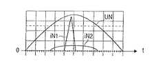
この回路の動作過程は、図2に参照して説明される。図2aは、電源ライン電圧UNの一つの半サイクルを示す。特に考慮をしていないスイッチモード電源は、最大UNの、パルス形で発生するiN1を電源ラインからとり出す。
【0016】
この電流は、電源ラインの高調波負荷の既存または将来的な規制に矛盾する。そのとき電流iN2は、図1の補助電流調節の結果、望ましい動作で電源ラインから出る。電流iN2は、電源ラインの半サイクルの間、長い持続と小さい増幅となり、UNに比例する非常に良い近似に理想波形になる。
【0017】
図2bによる電荷コンデンサCNの電圧UCNは、相当する小容量電荷コンデンサCNの電力係数[sic]の結果として、発振している正弦波電圧である。しかしながら、正弦波電圧は、UNの0交差の範囲で0に落ちないが、そこで一定した値を保つ。大容量蓄電コンデンサCSの電圧UCSは、実際に半サイクルの間ドロップしない、フィルタされたDC電圧である。ダイオードDNは、CSに対する第一充電パスを構成する。しかし、ダイオードDN自身は、望ましくない高長波を持つ電流iN1を出す。そのときLHとDHで構成された直列回路は、CSに対する第二充電パスを構成する。LHの値とピックオフAの特別な選択の結果として、補助充電電流が、UNの最大の範囲でCSに流れる。この充電電流は、より長い持続と、iN1よりも小さい増幅を保つ。そのために電源ラインから出る電流は、例えば図2aのように、形iN1から形iN2へ転換される。
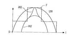
【0018】
図2dは、電源ラインから出る電流に対する規制を表わすウインドウFを示す。短い持続のために、図2aによる電流iN1は、このウインドウの中に置かれ、望んでいるようなiN2の形を想定しない。しかし図2dによる電流iN2は、ウインドウFによって構成されたエッジを越えて、十分長く持続を保つために、要求される形になる。図2によるiN2は、もしダイオードDNが逆バイアスで存続したり、備えられないとき流れる。
【0019】
もしDNが、補助的な正バイアスであるならば、電流iN3はまた更に流れる。
【0020】
CSに対する充電パスのような機能に加えて、ダイオードDNはまた、以下のような有利な効果を持つ。:DNの影響の結果として、実際問題、電圧VCNは、CSの電圧UCSよりも正になることができない。一方、実際問題、電圧UCSは、大容量蓄電コンデンサCSのために、パルスのように変化できない。結果として、電源ライン整流器BRの出力や電荷コンデンサCNの妨害パルスNは、望ましい方法でこのように抑えられる。
【0021】
図3は、ピックオフAの実装に関して、図1による回路の変更を示す。ピックオフAは、トランスTrの補助コイルW3で構成される。補助コイルW3は、三つの並列接続されたコイル部W3a、W3b、W3cから構成する。一次コイルW1は、三つのコイル部W1a、W1b、W1cと同様に分けられる。二つの対応したコイル部、すなわちW1aとW3a、W1bとW3b、W1cとW3cは、各々チャンバーコイル構成器の一つのチャンバーの中に一緒に置かれる。チャンバーコイル構成器は、コイル間で特に閉対となり、製造技術の点から経済的に生産できる。図3による解決は、補助接続ピンまたは明らかにピックオフAのピンの一つだけが、トランスTrで必要とされる。一方、図3による回路は、図1による回路と同じ方法で動作する。
【0022】
図4は、トランスTrの一例である。チャンバートランスは、個々のチャンバーに対して分かれた一次コイルと並列に置かれる。これらタッピングコイルは、並列に接続される。
【0023】
図5は、トランスTrのタッピングの更に進んだ例を示す。タッピングコイルは、並列に接続され、一次コイルのタッピングに補助的に接続される。
【0024】
図6は、この発明の発展を示す。この回路は、図1による回路と同じ方法で構成される。しかし、この回路は絶縁トランスを持たないが、ステップダウン回路と呼ばれるように構成される。この場合に、図1と同じ部分は、同じ参照シンボルで示される。スイッチングトランジスタT1までの回路の左手部分は、電源ラインの高調波負荷を軽減するために使われる。スイッチングトランジスタからの回路の右手部分は、負荷R2の動作電圧UBを何度も出すステップダウン回路と呼ばれる。トランスTr2の二次コイルW2は、ステップダウン回路のインダクタンスを構成する上記トランスTr2の一次コイルW1である、インダクタンスLHに直列に接続される。電源ラインの高調波負荷のような、高調波負荷を軽減するために、ステップダウン回路からその回路にフィードバックする結果として、1サイクルの間、電源ライン整流器BRから持続して流れるその電流は、何度も拡大される。図6による回路は、複数の利点がある。
【0025】
高調波負荷を軽減する回路と図6によるステップダウン回路の組合せの結果として、前もって必要とされる複数の部品が不要となる。特に、一つのスイッチングトランジスタT1だけは、既知の回路と比較して、両方の回路で必要とされる。例えば具体的に言うと、インダクタンスLHは、既知の回路と比較して、500μHから75μHに、かなり減らされる。一つのスイッチングトランジスタT1だけが、両方の回路で使われていることの結果として、一つの制御回路はまた全体に渡ることを必要とされる。図6による回路は、特に説明した負荷R2を意味する、メタルhalideランプを制御するためには適切である。トランスTr2の巻率は、およそW1:S2=2:1である。
【0026】
図7は、図6による回路を簡単にした例を示す。
【0027】
図6に説明されたインダクタンスLHは、トランスTr2の二次コイルW2がインダクタンスから離れて構成されたが、図7ではもはや必要とされない。結果としてインダクタンスLHは、インダクタンスの構成で離れた部品として、もはや必要とされない。
【0028】
図8は、トランスTr2の実際の例を示す。一次コイルW1と二次コイルW2は、チャンバーコイル構成器Cの二つのチャンバーK1とK2の中に置かれる。チャンバーK1とK2は、巻かれない中間空間Bを用いて、コイル構成器Cの軸方向に互いに別々の場所に置かれる。インダクタンスLHを実装するための、二次コイルW2に対する離れたインダクタンスは、この分離部Bの選択によって調節できる。
【0029】
実際に試験した回路の場合、部品は以下の値にした。
CN:0.7μF
CS:100μF
LH:300μH(図6のみ75μH)
【図面の簡単な説明】
【図1】この発明の模範的具体例を示す。
【図2a】図1による回路の動作過程を説明するためのグラフを示す。
【図2b】図1による回路の動作過程を説明するためのグラフを示す。
【図2c】図1による回路の動作過程を説明するためのグラフを示す。
【図2d】図1による回路の動作過程を説明するためのグラフを示す。
【図3】この発明の発展例を示す。
【図4】この発明の別の実施例を示す。
【図5】この発明の別の実施例を示す。
【図6】この発明の別の実施例を示す。
【図7】図6による回路を簡単にした変更を示す。
【図8】図6と図7による回路で使われたトランスの物理的な図を示す。
【符号の説明】
LH インダクタンス
DH ダイオード
Tr トランス
A 一次コイルのピックオフ
W1 一次コイル
CN、DN 電荷コンデンサ
UN 電源ライン電圧
CS 蓄電コンデンサ[0001]
BACKGROUND OF THE INVENTION
The present invention relates to a switch mode power supply.
[0002]
[Prior art]
The switch mode power supply provides a heavy pulse load, that is, a load having harmonics, to the power supply line. Such a load on the power supply line is preferred because the existing network is not fully available as a result of the skin effect that generates significant reactance currents and interferes with the information sent auxiliary via the network. Absent. Internationally, therefore, there are stricter regulations on the maximum harmonic load of power lines. The harmonic load is also called power count [sic].
[0003]
The harmonic load of the power line can be reduced by inserting a relatively large inductance between the power line terminal and the power line rectifier. However, such inductance is a relatively large and expensive component.
[0004]
[Problems to be solved by the invention]
The present invention is based on the object of developing a switch mode power supply using simple circuit components that reduces the harmonic load on the power line and can accommodate existing or future harmonic load regulations. ing.
[0005]
[Means for Solving the Problems]
In the case of the present invention, first of all, the charge capacitor at the output of the power line rectifier has a very small capacity and the voltage is a half-wave sine wave voltage of constant polarity that is not filtered. An actual storage capacitor with a very large capacity, whose voltage is a filtered DC voltage without a valid AC voltage component, is connected in parallel to a series circuit consisting of the primary coil of the transformer and a switching transistor Is done. The small-capacity charge capacitor and the large-capacity storage capacitor are either non-interfering with each other because they are either completely insulated from each other or connected to each other via a non-interfering diode.
[0006]
In addition, the charge capacitor is connected to the primary coil pickoff via a series circuit composed of an inductance and a diode.
[0007]
A series circuit composed of an inductance and a diode constitutes an auxiliary charging path for the storage capacitor. As designed, the current flowing through this charging path lasts considerably longer than the normal flowing pulse charging current. As a result, the harmonic loading of the power line is further reduced by the current leaving the power line that approximates the ideal current corresponding to the power line voltage. The width, ie the duration of this current during one half cycle of the power supply line, can be adjusted by the choice of primary coil pick-off, ie the turns of the two coil parts of the primary coil. On the other hand, the current amplification can be adjusted by the inductance value. Thus, the charge capacitor constitutes a direct voltage source for the auxiliary charging current for the large-capacity storage capacitor in order to reduce harmonics.
[0008]
The circuit according to the invention is relatively simple since essentially only one inductance and two diodes are required. The circuit can achieve the optimum harmonic load magnitude, particularly as a result of the magnitude of the inductance and the choice of transformer primary coil pickoff. Since this inductance sends only a portion of the electric charge for the storage capacitor, this inductance can be made relatively small. A further advantage is that when the invention is applied to an existing switch mode power supply, no substantial changes are required with respect to regulation and control. It is a further advantage that a high level of stability against pulse spikes is achieved as a result of the large capacity storage capacitor being retained.
[0009]
The charge capacitor and the storage capacitor are insulated from each other using a non-interfering diode. In this case, the diode has a dual function. One is used as a charging path for the storage capacitor, and the other is used to suppress the pulsed disturbance voltage of the charge capacitor. This diode can also be omitted as much as possible. The charge capacitor is then connected only to the output of the storage capacitor to the power line rectifier and primary coil. This has no connection between these two capacitors, except for a series circuit consisting of an inductance and a diode.
[0010]
For example, the winding ratio between the primary coil portion between the pick-off and the switching transistor and the coil portion between the pick-off and the end of the primary coil connected to the storage capacitor is 2: 1. That rate determines the duration of the auxiliary charging current during one power cycle.
[0011]
The primary coil pickoff also consists of one of the ends of the auxiliary coil of the transformer, the other end connected to one of the ends of the primary coil. In this case, a plurality of parallel connection auxiliary coils are provided. In this case, the primary coil itself is divided into a large number of coil portions placed in individual chambers of the chamber coil construction device and auxiliary coils placed in the respective chambers. Such a chamber coil construction device is manufactured in a closed pair between coils. In this solution, only one auxiliary pin is required in the transformer.
[0012]
The small charge capacitor preferably has a capacity of approximately 0.5 μF, while the large charge capacitor has a capacity of approximately 100 μF.
[0013]
In this case, the charge capacitor does not drop to zero in the range of the zero crossing of the power supply line voltage, but instead has a capacitance that maintains a constant value there.
[0014]
DETAILED DESCRIPTION OF THE INVENTION
FIG. 1 shows the configuration of a switch mode power supply. This figure shows a power line voltage UN, a power line rectifier BR, a current limiting resistor R1, a charge capacitor CN, a transformer Tr having a primary coil W1 and a secondary coil W2, a switching transistor T1, a load R2, and a filter for the control circuit S. It is composed of a diode D1 that outputs an operating voltage UB of the capacitor C1. The control circuit S is supplied by the secondary coil and controls switching of the function for stabilizing the operating voltage UB. The charge capacitor CN and the storage capacitor CS are non-interfering with each other using the decoupling diode DN. In addition, the series circuit composed of the inductance LH and the diode DH is inserted between the charge capacitor CN and the pick-off A of the primary coil W1.
[0015]
The operation process of this circuit will be described with reference to FIG. FIG. 2a shows one half cycle of the power supply line voltage UN. A switch mode power supply not particularly considered takes out iN1 generated in a pulse form with a maximum UN from the power supply line.
[0016]
This current is inconsistent with existing or future regulations on power line harmonic loads. At that time, the current iN2 exits the power supply line in a desirable operation as a result of the auxiliary current adjustment of FIG. The current iN2 has a long duration and small amplification during a half cycle of the power line, making it an ideal waveform for a very good approximation proportional to UN.
[0017]
The voltage UCN of the charge capacitor CN according to FIG. 2b is a sinusoidal voltage oscillating as a result of the power coefficient [sic] of the corresponding small-capacity charge capacitor CN. However, the sinusoidal voltage does not drop to zero in the range of the UN zero crossing, but remains constant there. The voltage UCS of the large storage capacitor CS is a filtered DC voltage that does not actually drop for half a cycle. The diode DN constitutes a first charging path for CS. However, the diode DN itself produces a current iN1 with an undesirable high long wave. At that time, the series circuit composed of LH and DH constitutes a second charging path for CS. As a result of the special selection of the value of LH and pickoff A, the auxiliary charging current flows to CS in the maximum range of UN. This charging current keeps longer duration and amplification smaller than iN1. For this purpose, the current emanating from the power supply line is converted from form iN1 to form iN2, for example as shown in FIG. 2a.
[0018]
FIG. 2d shows a window F representing the regulation for the current leaving the power supply line. For short duration, the current iN1 according to FIG. 2a is placed in this window and does not assume the shape of iN2 as desired. However, the current iN2 according to FIG. 2d takes the form required to remain long enough beyond the edge formed by the window F. The iN2 according to FIG. 2 flows if the diode DN persists in reverse bias or is not provided.
[0019]
If DN is an auxiliary positive bias, current iN3 will still flow.
[0020]
In addition to functions such as a charging path for CS, the diode DN also has the following advantageous effects. : As a result of the influence of DN, the actual problem, the voltage VCN cannot be more positive than the voltage UCS of CS. On the other hand, the actual problem, the voltage UCS cannot be changed like a pulse because of the large-capacity storage capacitor CS. As a result, the output of the power line rectifier BR and the disturbing pulse N of the charge capacitor CN are thus suppressed in a desirable manner.
[0021]
FIG. 3 shows a modification of the circuit according to FIG. The pickoff A is composed of an auxiliary coil W3 of the transformer Tr. The auxiliary coil W3 includes three coil parts W3a, W3b, and W3c connected in parallel. The primary coil W1 is divided in the same manner as the three coil portions W1a, W1b, and W1c. Two corresponding coil sections, W1a and W3a, W1b and W3b, W1c and W3c, are each placed together in one chamber of the chamber coil structure. The chamber coil constructer is particularly closed between the coils and can be produced economically in terms of manufacturing technology. The solution according to FIG. 3 requires only one of the auxiliary connection pins or apparently the pickoff A pins in the transformer Tr. On the other hand, the circuit according to FIG. 3 operates in the same way as the circuit according to FIG.
[0022]
FIG. 4 is an example of the transformer Tr. The chamber transformer is placed in parallel with the primary coil divided for each chamber. These tapping coils are connected in parallel.
[0023]
FIG. 5 shows a further advanced example of tapping of the transformer Tr. The tapping coils are connected in parallel and supplementarily connected to the tapping of the primary coil.
[0024]
FIG. 6 shows the development of this invention. This circuit is constructed in the same way as the circuit according to FIG. However, this circuit does not have an isolation transformer, but is configured to be called a step-down circuit. In this case, the same parts as those in FIG. 1 are denoted by the same reference symbols. The left-hand part of the circuit up to the switching transistor T1 is used to reduce the harmonic load of the power supply line. The right-hand part of the circuit from the switching transistor is called a step-down circuit that repeatedly outputs the operating voltage UB of the load R2. The secondary coil W2 of the transformer Tr2 is connected in series to the inductance LH, which is the primary coil W1 of the transformer Tr2 constituting the inductance of the step-down circuit. As a result of feedback from the step-down circuit to the circuit to reduce the harmonic load, such as the power line harmonic load, what is the current that flows continuously from the power line rectifier BR for one cycle? The degree is also expanded. The circuit according to FIG. 6 has several advantages.
[0025]
As a result of the combination of the circuit for reducing the harmonic load and the step-down circuit according to FIG. 6, a plurality of parts required in advance are not required. In particular, only one switching transistor T1 is required in both circuits compared to known circuits. For example, specifically, the inductance LH is significantly reduced from 500 μH to 75 μH compared to known circuits. As a result of only one switching transistor T1 being used in both circuits, one control circuit is also required throughout. The circuit according to FIG. 6 is particularly suitable for controlling a metal halide lamp, which means the load R2 described. The winding ratio of the transformer Tr2 is approximately W1: S2 = 2: 1.
[0026]
FIG. 7 shows a simplified example of the circuit according to FIG.
[0027]
The inductance LH illustrated in FIG. 6 is not required in FIG. 7 although the secondary coil W2 of the transformer Tr2 is configured away from the inductance. As a result, the inductance LH is no longer needed as a separate component in the inductance configuration.
[0028]
FIG. 8 shows an actual example of the transformer Tr2. The primary coil W1 and the secondary coil W2 are placed in the two chambers K1 and K2 of the chamber coil constructer C. The chambers K1 and K2 are placed at different locations in the axial direction of the coil construction device C using the intermediate space B that is not wound. The inductance away from the secondary coil W2 for mounting the inductance LH can be adjusted by the selection of the separation part B.
[0029]
For the actual tested circuit, the components were set to the following values:
CN: 0.7 μF
CS: 100 μF
LH: 300 μH (75 μH in FIG. 6 only)
[Brief description of the drawings]
FIG. 1 shows an exemplary embodiment of the present invention.
2a shows a graph for explaining the operation process of the circuit according to FIG.
2b shows a graph for explaining the operation process of the circuit according to FIG.
FIG. 2c shows a graph for explaining the operation process of the circuit according to FIG.
FIG. 2d shows a graph for explaining the operation process of the circuit according to FIG.
FIG. 3 shows a development example of the present invention.
FIG. 4 shows another embodiment of the present invention.
FIG. 5 shows another embodiment of the present invention.
FIG. 6 shows another embodiment of the present invention.
FIG. 7 shows a modification of the circuit according to FIG.
8 shows a physical diagram of the transformer used in the circuit according to FIGS. 6 and 7. FIG.
[Explanation of symbols]
LH Inductance DH Diode Tr Transformer A Primary coil pickoff W1 Primary coils CN, DN Charge capacitor UN Power supply line voltage CS Storage capacitor
Claims (11)
Translated fromJapanese(a) 電荷コンデンサ(CN)は、非常に小さく、その電圧(UCS)はフィルタされない一定極性の半波正弦波電圧であり、
(b) 蓄電コンデンサ(CS)は、直列回路(W1、T1)に対して並列に接続され、その容量は非常に大きく、その電圧(UCS)はフィルタされたDC電圧であり、
(c) 電荷コンデンサ(CN)は、インダクタンス(LH)とダイオード(DH)で構成された直列回路を経由して、一次コイル(W1)のピックオフ(A)に接続され、
(d) デカップリング素子(DN)が、電荷コンデンサ(CN)と蓄電コンデンサ(CS)の間に接続されることを特徴とする、電源ラインの高調波負荷を軽減したスイッチモード電源。The output of the power line rectifier (BR) is connected to a series circuit composed of a charge capacitor (CN), a main coil (W1) of a transformer (Tr) and a switching transistor (T1),
(A) The charge capacitor (CN) is very small and its voltage (UCS) is an unfiltered constant polarity half wave sine wave voltage;
(B) The storage capacitor (CS) is connected in parallel to the series circuit (W1, T1), its capacity is very large, its voltage (UCS) is a filtered DC voltage,
(C) The charge capacitor (CN) is connected to the pick-off (A) of the primary coil (W1) via a series circuit composed of an inductance (LH) and a diode (DH),
(D) A switch mode power supply with reduced harmonic load on the power supply line, wherein the decoupling element (DN) is connected between the charge capacitor (CN) and the storage capacitor (CS).
スイッチングトランジスタが、動作電圧(UB)を供給するフィルタコンデンサ(C1)に、第二インダクタンス(W1)を経由して接続され、
第二インダクタンス(W1)と対になった第三インダクタンス(W2)が、第一インダクタンス(LH)と直列に接続された、電源ラインの高調波負荷を軽減したスイッチモード電源。The output of the power line rectifier (BR) is connected to the switching transistor via a charge capacitor (CN), a series circuit composed of a first inductance (LH) and a diode (DH),
A switching transistor is connected via a second inductance (W1) to a filter capacitor (C1) that supplies an operating voltage (UB),
A switch mode power supply in which the third inductance (W2) paired with the second inductance (W1) is connected in series with the first inductance (LH) and the harmonic load of the power supply line is reduced.
二つのチャンバー(K1、K2)が、巻線のない中間空間(B)を用いて、軸方向に互いに分けて置かれた、請求項10に記載の電源。The primary coil (W1) and the secondary coil (W2) of the transformer (Tr2) are placed in the two chambers (K1, K2) of the chamber coil structure (C),
11. The power supply according to claim 10, wherein the two chambers (K1, K2) are placed separately from each other in the axial direction using an intermediate space (B) without windings.
Applications Claiming Priority (4)
| Application Number | Priority Date | Filing Date | Title |
|---|---|---|---|
| DE4431120.6 | 1994-09-01 | ||
| DE4431120ADE4431120A1 (en) | 1994-09-01 | 1994-09-01 | Switched-mode power supply unit reducing mains harmonic loading |
| DE19502647.0 | 1995-01-28 | ||
| DE19502647 | 1995-01-28 |
Publications (2)
| Publication Number | Publication Date |
|---|---|
| JPH0880032A JPH0880032A (en) | 1996-03-22 |
| JP3622284B2true JP3622284B2 (en) | 2005-02-23 |
Family
ID=25939747
Family Applications (1)
| Application Number | Title | Priority Date | Filing Date |
|---|---|---|---|
| JP24052895AExpired - LifetimeJP3622284B2 (en) | 1994-09-01 | 1995-08-28 | Switch-mode power supply circuit that reduces the load on the power supply line due to harmonics |
Country Status (6)
| Country | Link |
|---|---|
| US (1) | US5673184A (en) |
| EP (1) | EP0700145B1 (en) |
| JP (1) | JP3622284B2 (en) |
| KR (1) | KR100379056B1 (en) |
| CN (1) | CN1041263C (en) |
| DE (1) | DE59502158D1 (en) |
Families Citing this family (27)
| Publication number | Priority date | Publication date | Assignee | Title |
|---|---|---|---|---|
| US5652700A (en)* | 1995-10-16 | 1997-07-29 | Computer Products, Inc. | Low cost AC-to-DC converter having input current with reduced harmonics |
| DE19610762A1 (en)* | 1996-03-19 | 1997-09-25 | Thomson Brandt Gmbh | Switching power supply with reduced harmonic load on the network |
| JPH1155943A (en)* | 1997-06-02 | 1999-02-26 | Murata Mfg Co Ltd | Switching power unit |
| US6005780A (en)* | 1997-08-29 | 1999-12-21 | Hua; Guichao | Single-stage AC/DC conversion with PFC-tapped transformers |
| DE19747801A1 (en)* | 1997-10-30 | 1999-05-06 | Thomson Brandt Gmbh | Switching power supply |
| US6570505B1 (en) | 1997-12-30 | 2003-05-27 | Gelcore Llc | LED lamp with a fault-indicating impedance-changing circuit |
| JP2991181B2 (en)* | 1998-02-27 | 1999-12-20 | 富士電機株式会社 | Switching power supply |
| US6115273A (en) | 1998-07-09 | 2000-09-05 | Illinois Tool Works Inc. | Power converter with low loss switching |
| US6865096B1 (en) | 1998-07-09 | 2005-03-08 | Illinois Tool Works Inc. | Power convertor with low loss switching |
| JP2001095253A (en) | 1999-09-24 | 2001-04-06 | Sony Corp | Switching power circuit |
| CA2306531C (en)* | 1999-10-15 | 2011-07-12 | Wayne Ernest Conrad | Method and apparatus for delivering power to mechanical or electrical system |
| JP3402361B2 (en)* | 1999-12-28 | 2003-05-06 | 横河電機株式会社 | Switching power supply |
| CA2306291A1 (en) | 2000-04-20 | 2001-10-20 | Wayne Ernest Conrad | Method and apparatus for improving the speed and fuel economy ¬hence endurance (range)| of aircraft, surface vessels, sub-surface vessels, missiles and torpedoes and/or altering the acoustic signature of such aircraft, surface vessels, sub-surface vessels, missiles or torpedoes |
| WO2002075779A2 (en) | 2001-03-16 | 2002-09-26 | Thomson Licensing S.A. | Power supply with a reduced harmonic load on the mains system, and a corresponding appliance |
| DE10135599A1 (en) | 2001-07-20 | 2003-02-13 | Thomson Brandt Gmbh | Switched-mode power supply with power factor correction, and coil for a corresponding correction circuit |
| JP2003149242A (en)* | 2001-11-09 | 2003-05-21 | Gifu Univ | Antibody detection method and antigen microarray |
| JP2004040995A (en)* | 2002-06-28 | 2004-02-05 | Oce Technol Bv | Method and apparatus for controlling power supplied to load |
| EP1376845A1 (en)* | 2002-06-28 | 2004-01-02 | Océ-Technologies B.V. | Method and apparatus for controlling the power supplied to a load |
| US20040190213A1 (en)* | 2003-03-24 | 2004-09-30 | Kuo-Liang Lin | Compensation circuit for power supply |
| JP4280976B2 (en)* | 2003-04-10 | 2009-06-17 | 横河電機株式会社 | Switching power supply |
| GB0402319D0 (en)* | 2004-02-03 | 2004-03-10 | M & Fc Holdings Llc | Wide range power supply for polyphase electricity meter |
| CN101114541B (en)* | 2006-07-28 | 2011-05-25 | 台达电子工业股份有限公司 | power conversion device |
| WO2009144784A1 (en)* | 2008-05-27 | 2009-12-03 | 富士通メディアデバイス株式会社 | Switch circuit |
| CN101686015B (en)* | 2008-09-23 | 2011-12-28 | 台达电子工业股份有限公司 | Forward-Flyback Converter with Active Clamp |
| RU2414804C1 (en)* | 2010-01-18 | 2011-03-20 | Общество с ограниченной ответственностью "Технологическая лаборатория" | Test bench of electric energy sources |
| CN102420456A (en)* | 2011-09-29 | 2012-04-18 | 特变电工新疆新能源股份有限公司 | Power supply system for photovoltaic grid-connected inverter |
| CN102714464B (en)* | 2012-02-29 | 2014-04-02 | 深圳市核达中远通电源技术有限公司 | A multi-input DC converter and a PFC circuit |
Family Cites Families (14)
| Publication number | Priority date | Publication date | Assignee | Title |
|---|---|---|---|---|
| JPH0744840B2 (en)* | 1982-01-30 | 1995-05-15 | 松下電工株式会社 | Discharge lamp lighting device |
| JPS6485574A (en)* | 1987-09-28 | 1989-03-30 | Toshiba Corp | Power converting device |
| JPH01105381U (en)* | 1987-12-26 | 1989-07-17 | ||
| DE4008652C2 (en)* | 1990-03-17 | 2000-06-21 | Schneider Automation Gmbh | Power supply unit with DC-DC converter |
| DE59009728D1 (en)* | 1990-07-03 | 1995-11-02 | Siemens Ag | Circuit arrangement for a free-running flyback converter switching power supply. |
| DE4025322A1 (en)* | 1990-08-10 | 1992-02-13 | Thomson Brandt Gmbh | MAINS OPERATED PHASE CONTROL CONTROL |
| JP2697748B2 (en)* | 1990-09-19 | 1998-01-14 | 株式会社日立製作所 | Power supply |
| JP3232593B2 (en)* | 1991-08-22 | 2001-11-26 | 松下電工株式会社 | Power supply |
| US5301095A (en)* | 1991-10-01 | 1994-04-05 | Origin Electric Company, Limited | High power factor AC/DC converter |
| US5331534A (en)* | 1991-11-20 | 1994-07-19 | Tokyo Electric Co., Ltd. | Power supply apparatus |
| GB9219663D0 (en)* | 1992-09-17 | 1992-10-28 | Rca Thomson Licensing Corp | Switch mode power supply with low input current distortion |
| DE4238808C2 (en)* | 1992-11-17 | 1996-12-19 | Siemens Ag | Flyback converter switched-mode power supply with sinusoidal current consumption |
| JP2767781B2 (en)* | 1993-09-17 | 1998-06-18 | 東光株式会社 | AC-DC converter |
| JP3287086B2 (en)* | 1993-12-17 | 2002-05-27 | 株式会社ニプロン | Switching regulator |
- 1995
- 1995-05-31USUS08/454,931patent/US5673184A/ennot_activeExpired - Lifetime
- 1995-08-14CNCN95115358Apatent/CN1041263C/ennot_activeExpired - Lifetime
- 1995-08-19EPEP95113076Apatent/EP0700145B1/ennot_activeExpired - Lifetime
- 1995-08-19DEDE59502158Tpatent/DE59502158D1/ennot_activeExpired - Lifetime
- 1995-08-28JPJP24052895Apatent/JP3622284B2/ennot_activeExpired - Lifetime
- 1995-09-01KRKR1019950028561Apatent/KR100379056B1/ennot_activeExpired - Lifetime
Also Published As
| Publication number | Publication date |
|---|---|
| JPH0880032A (en) | 1996-03-22 |
| EP0700145A2 (en) | 1996-03-06 |
| KR960012677A (en) | 1996-04-20 |
| KR100379056B1 (en) | 2003-06-09 |
| EP0700145A3 (en) | 1996-08-28 |
| US5673184A (en) | 1997-09-30 |
| EP0700145B1 (en) | 1998-05-13 |
| CN1125361A (en) | 1996-06-26 |
| CN1041263C (en) | 1998-12-16 |
| DE59502158D1 (en) | 1998-06-18 |
Similar Documents
| Publication | Publication Date | Title |
|---|---|---|
| JP3622284B2 (en) | Switch-mode power supply circuit that reduces the load on the power supply line due to harmonics | |
| US4563731A (en) | Resonant type constant voltage supply apparatus | |
| US4564897A (en) | Power source | |
| US4782268A (en) | Low-pressure discharge lamp, particularly fluorescent lamp high-frequency operating circuit with low-power network interference | |
| KR0155147B1 (en) | Inverter apparatus | |
| US7071632B2 (en) | Discharge lamp starter | |
| JP2002199718A (en) | Resonance-type switching power supply device | |
| US6337800B1 (en) | Electronic ballast with inductive power feedback | |
| JPH06245530A (en) | Power device | |
| US5635800A (en) | Ballast circuit with a japped transformer flyback converter providing driving energy for start, glow and run modes of a lamp | |
| JPH05176532A (en) | Power circuit | |
| JP2004534659A (en) | Generator for power factor 1 arc welding machine | |
| GB2133940A (en) | AC-DC-AC converter | |
| US5117176A (en) | Alternating current conditioner | |
| JP3354454B2 (en) | Switching power supply | |
| JPH0588067B2 (en) | ||
| JP3096229B2 (en) | Switching power supply | |
| JP3326660B2 (en) | Switching power supply circuit | |
| JPH10164861A (en) | Resonance inverter circuit | |
| JP3155882B2 (en) | Switching regulator | |
| JP3081417B2 (en) | Switching power supply | |
| JP2576174B2 (en) | No-load protection ballast with automatic adjustment function | |
| JPH0251361A (en) | Inverter apparatus | |
| JPH08149816A (en) | Switching power supply circuit | |
| JPH0678554A (en) | Inverter device |
Legal Events
| Date | Code | Title | Description |
|---|---|---|---|
| A131 | Notification of reasons for refusal | Free format text:JAPANESE INTERMEDIATE CODE: A131 Effective date:20040914 | |
| A521 | Request for written amendment filed | Free format text:JAPANESE INTERMEDIATE CODE: A523 Effective date:20040916 | |
| TRDD | Decision of grant or rejection written | ||
| A01 | Written decision to grant a patent or to grant a registration (utility model) | Free format text:JAPANESE INTERMEDIATE CODE: A01 Effective date:20041102 | |
| A61 | First payment of annual fees (during grant procedure) | Free format text:JAPANESE INTERMEDIATE CODE: A61 Effective date:20041115 | |
| R150 | Certificate of patent or registration of utility model | Free format text:JAPANESE INTERMEDIATE CODE: R150 | |
| FPAY | Renewal fee payment (event date is renewal date of database) | Free format text:PAYMENT UNTIL: 20071203 Year of fee payment:3 | |
| FPAY | Renewal fee payment (event date is renewal date of database) | Free format text:PAYMENT UNTIL: 20081203 Year of fee payment:4 | |
| FPAY | Renewal fee payment (event date is renewal date of database) | Free format text:PAYMENT UNTIL: 20091203 Year of fee payment:5 | |
| FPAY | Renewal fee payment (event date is renewal date of database) | Free format text:PAYMENT UNTIL: 20101203 Year of fee payment:6 | |
| FPAY | Renewal fee payment (event date is renewal date of database) | Free format text:PAYMENT UNTIL: 20101203 Year of fee payment:6 | |
| FPAY | Renewal fee payment (event date is renewal date of database) | Free format text:PAYMENT UNTIL: 20111203 Year of fee payment:7 | |
| FPAY | Renewal fee payment (event date is renewal date of database) | Free format text:PAYMENT UNTIL: 20111203 Year of fee payment:7 | |
| FPAY | Renewal fee payment (event date is renewal date of database) | Free format text:PAYMENT UNTIL: 20121203 Year of fee payment:8 | |
| FPAY | Renewal fee payment (event date is renewal date of database) | Free format text:PAYMENT UNTIL: 20121203 Year of fee payment:8 | |
| FPAY | Renewal fee payment (event date is renewal date of database) | Free format text:PAYMENT UNTIL: 20131203 Year of fee payment:9 | |
| R250 | Receipt of annual fees | Free format text:JAPANESE INTERMEDIATE CODE: R250 | |
| EXPY | Cancellation because of completion of term |