JP3617574B2 - Multiple-multi-row lead frame and method of manufacturing semiconductor device using the same - Google Patents
Multiple-multi-row lead frame and method of manufacturing semiconductor device using the sameDownload PDFInfo
- Publication number
- JP3617574B2 JP3617574B2JP15026596AJP15026596AJP3617574B2JP 3617574 B2JP3617574 B2JP 3617574B2JP 15026596 AJP15026596 AJP 15026596AJP 15026596 AJP15026596 AJP 15026596AJP 3617574 B2JP3617574 B2JP 3617574B2
- Authority
- JP
- Japan
- Prior art keywords
- lead
- frame
- frames
- lead frame
- row
- Prior art date
- Legal status (The legal status is an assumption and is not a legal conclusion. Google has not performed a legal analysis and makes no representation as to the accuracy of the status listed.)
- Expired - Fee Related
Links
- 239000004065semiconductorSubstances0.000titleclaimsdescription25
- 238000004519manufacturing processMethods0.000titleclaimsdescription17
- 238000000465mouldingMethods0.000claimsdescription40
- 229920005989resinPolymers0.000claimsdescription39
- 239000011347resinSubstances0.000claimsdescription39
- 238000007747platingMethods0.000claimsdescription31
- 238000007789sealingMethods0.000claimsdescription27
- 238000000034methodMethods0.000claimsdescription26
- 239000008188pelletSubstances0.000claimsdescription25
- 238000005192partitionMethods0.000claimsdescription18
- 238000005452bendingMethods0.000claimsdescription11
- 241000272168LaridaeSpecies0.000claimsdescription10
- 239000000725suspensionSubstances0.000claimsdescription9
- 229910000679solderInorganic materials0.000description33
- 238000009740moulding (composite fabrication)Methods0.000description19
- 238000003825pressingMethods0.000description13
- 239000011248coating agentSubstances0.000description11
- 238000000576coating methodMethods0.000description11
- 238000000638solvent extractionMethods0.000description10
- 238000001721transfer mouldingMethods0.000description6
- 239000000463materialSubstances0.000description5
- 230000013011matingEffects0.000description5
- RYGMFSIKBFXOCR-UHFFFAOYSA-NCopperChemical compound[Cu]RYGMFSIKBFXOCR-UHFFFAOYSA-N0.000description4
- XEEYBQQBJWHFJM-UHFFFAOYSA-NIronChemical compound[Fe]XEEYBQQBJWHFJM-UHFFFAOYSA-N0.000description4
- BQCADISMDOOEFD-UHFFFAOYSA-NSilverChemical compound[Ag]BQCADISMDOOEFD-UHFFFAOYSA-N0.000description4
- 229910052802copperInorganic materials0.000description4
- 239000010949copperSubstances0.000description4
- 230000007547defectEffects0.000description3
- 238000000151depositionMethods0.000description3
- 230000000694effectsEffects0.000description3
- 239000012778molding materialSubstances0.000description3
- 229910052709silverInorganic materials0.000description3
- 239000004332silverSubstances0.000description3
- 230000008646thermal stressEffects0.000description3
- 229910045601alloyInorganic materials0.000description2
- 239000000956alloySubstances0.000description2
- PCHJSUWPFVWCPO-UHFFFAOYSA-NgoldChemical compound[Au]PCHJSUWPFVWCPO-UHFFFAOYSA-N0.000description2
- 229910052737goldInorganic materials0.000description2
- 239000010931goldSubstances0.000description2
- 229910052742ironInorganic materials0.000description2
- 239000007788liquidSubstances0.000description2
- 238000012545processingMethods0.000description2
- 229910001020Au alloyInorganic materials0.000description1
- 229910000881Cu alloyInorganic materials0.000description1
- 229910000831SteelInorganic materials0.000description1
- ATJFFYVFTNAWJD-UHFFFAOYSA-NTinChemical compound[Sn]ATJFFYVFTNAWJD-UHFFFAOYSA-N0.000description1
- 239000000853adhesiveSubstances0.000description1
- 230000001070adhesive effectEffects0.000description1
- 238000013459approachMethods0.000description1
- 230000000712assemblyEffects0.000description1
- 238000000429assemblyMethods0.000description1
- 230000000903blocking effectEffects0.000description1
- 238000005336crackingMethods0.000description1
- 238000007598dipping methodMethods0.000description1
- 239000008393encapsulating agentSubstances0.000description1
- 239000003822epoxy resinSubstances0.000description1
- 238000005530etchingMethods0.000description1
- 239000003353gold alloySubstances0.000description1
- 238000010438heat treatmentMethods0.000description1
- 238000002347injectionMethods0.000description1
- 239000007924injectionSubstances0.000description1
- 238000002156mixingMethods0.000description1
- 238000012986modificationMethods0.000description1
- 230000004048modificationEffects0.000description1
- 238000012536packaging technologyMethods0.000description1
- 229920000647polyepoxidePolymers0.000description1
- 238000004080punchingMethods0.000description1
- 230000002040relaxant effectEffects0.000description1
- 239000000243solutionSubstances0.000description1
- 239000002904solventSubstances0.000description1
- 239000010959steelSubstances0.000description1
- 229920001187thermosetting polymerPolymers0.000description1
Images


Classifications
- H—ELECTRICITY
- H01—ELECTRIC ELEMENTS
- H01L—SEMICONDUCTOR DEVICES NOT COVERED BY CLASS H10
- H01L24/00—Arrangements for connecting or disconnecting semiconductor or solid-state bodies; Methods or apparatus related thereto
- H01L24/93—Batch processes
- H01L24/95—Batch processes at chip-level, i.e. with connecting carried out on a plurality of singulated devices, i.e. on diced chips
- H01L24/97—Batch processes at chip-level, i.e. with connecting carried out on a plurality of singulated devices, i.e. on diced chips the devices being connected to a common substrate, e.g. interposer, said common substrate being separable into individual assemblies after connecting
- H—ELECTRICITY
- H01—ELECTRIC ELEMENTS
- H01L—SEMICONDUCTOR DEVICES NOT COVERED BY CLASS H10
- H01L2224/00—Indexing scheme for arrangements for connecting or disconnecting semiconductor or solid-state bodies and methods related thereto as covered by H01L24/00
- H01L2224/01—Means for bonding being attached to, or being formed on, the surface to be connected, e.g. chip-to-package, die-attach, "first-level" interconnects; Manufacturing methods related thereto
- H01L2224/26—Layer connectors, e.g. plate connectors, solder or adhesive layers; Manufacturing methods related thereto
- H01L2224/31—Structure, shape, material or disposition of the layer connectors after the connecting process
- H01L2224/32—Structure, shape, material or disposition of the layer connectors after the connecting process of an individual layer connector
- H01L2224/321—Disposition
- H01L2224/32151—Disposition the layer connector connecting between a semiconductor or solid-state body and an item not being a semiconductor or solid-state body, e.g. chip-to-substrate, chip-to-passive
- H01L2224/32221—Disposition the layer connector connecting between a semiconductor or solid-state body and an item not being a semiconductor or solid-state body, e.g. chip-to-substrate, chip-to-passive the body and the item being stacked
- H01L2224/32245—Disposition the layer connector connecting between a semiconductor or solid-state body and an item not being a semiconductor or solid-state body, e.g. chip-to-substrate, chip-to-passive the body and the item being stacked the item being metallic
- H—ELECTRICITY
- H01—ELECTRIC ELEMENTS
- H01L—SEMICONDUCTOR DEVICES NOT COVERED BY CLASS H10
- H01L2224/00—Indexing scheme for arrangements for connecting or disconnecting semiconductor or solid-state bodies and methods related thereto as covered by H01L24/00
- H01L2224/01—Means for bonding being attached to, or being formed on, the surface to be connected, e.g. chip-to-package, die-attach, "first-level" interconnects; Manufacturing methods related thereto
- H01L2224/42—Wire connectors; Manufacturing methods related thereto
- H01L2224/47—Structure, shape, material or disposition of the wire connectors after the connecting process
- H01L2224/48—Structure, shape, material or disposition of the wire connectors after the connecting process of an individual wire connector
- H01L2224/4805—Shape
- H01L2224/4809—Loop shape
- H01L2224/48091—Arched
- H—ELECTRICITY
- H01—ELECTRIC ELEMENTS
- H01L—SEMICONDUCTOR DEVICES NOT COVERED BY CLASS H10
- H01L2224/00—Indexing scheme for arrangements for connecting or disconnecting semiconductor or solid-state bodies and methods related thereto as covered by H01L24/00
- H01L2224/01—Means for bonding being attached to, or being formed on, the surface to be connected, e.g. chip-to-package, die-attach, "first-level" interconnects; Manufacturing methods related thereto
- H01L2224/42—Wire connectors; Manufacturing methods related thereto
- H01L2224/47—Structure, shape, material or disposition of the wire connectors after the connecting process
- H01L2224/48—Structure, shape, material or disposition of the wire connectors after the connecting process of an individual wire connector
- H01L2224/481—Disposition
- H01L2224/48151—Connecting between a semiconductor or solid-state body and an item not being a semiconductor or solid-state body, e.g. chip-to-substrate, chip-to-passive
- H01L2224/48221—Connecting between a semiconductor or solid-state body and an item not being a semiconductor or solid-state body, e.g. chip-to-substrate, chip-to-passive the body and the item being stacked
- H01L2224/48245—Connecting between a semiconductor or solid-state body and an item not being a semiconductor or solid-state body, e.g. chip-to-substrate, chip-to-passive the body and the item being stacked the item being metallic
- H01L2224/48247—Connecting between a semiconductor or solid-state body and an item not being a semiconductor or solid-state body, e.g. chip-to-substrate, chip-to-passive the body and the item being stacked the item being metallic connecting the wire to a bond pad of the item
- H—ELECTRICITY
- H01—ELECTRIC ELEMENTS
- H01L—SEMICONDUCTOR DEVICES NOT COVERED BY CLASS H10
- H01L2224/00—Indexing scheme for arrangements for connecting or disconnecting semiconductor or solid-state bodies and methods related thereto as covered by H01L24/00
- H01L2224/01—Means for bonding being attached to, or being formed on, the surface to be connected, e.g. chip-to-package, die-attach, "first-level" interconnects; Manufacturing methods related thereto
- H01L2224/42—Wire connectors; Manufacturing methods related thereto
- H01L2224/47—Structure, shape, material or disposition of the wire connectors after the connecting process
- H01L2224/48—Structure, shape, material or disposition of the wire connectors after the connecting process of an individual wire connector
- H01L2224/484—Connecting portions
- H01L2224/48463—Connecting portions the connecting portion on the bonding area of the semiconductor or solid-state body being a ball bond
- H01L2224/48465—Connecting portions the connecting portion on the bonding area of the semiconductor or solid-state body being a ball bond the other connecting portion not on the bonding area being a wedge bond, i.e. ball-to-wedge, regular stitch
- H—ELECTRICITY
- H01—ELECTRIC ELEMENTS
- H01L—SEMICONDUCTOR DEVICES NOT COVERED BY CLASS H10
- H01L2224/00—Indexing scheme for arrangements for connecting or disconnecting semiconductor or solid-state bodies and methods related thereto as covered by H01L24/00
- H01L2224/01—Means for bonding being attached to, or being formed on, the surface to be connected, e.g. chip-to-package, die-attach, "first-level" interconnects; Manufacturing methods related thereto
- H01L2224/42—Wire connectors; Manufacturing methods related thereto
- H01L2224/47—Structure, shape, material or disposition of the wire connectors after the connecting process
- H01L2224/49—Structure, shape, material or disposition of the wire connectors after the connecting process of a plurality of wire connectors
- H01L2224/491—Disposition
- H01L2224/4912—Layout
- H01L2224/49171—Fan-out arrangements
- H—ELECTRICITY
- H01—ELECTRIC ELEMENTS
- H01L—SEMICONDUCTOR DEVICES NOT COVERED BY CLASS H10
- H01L2224/00—Indexing scheme for arrangements for connecting or disconnecting semiconductor or solid-state bodies and methods related thereto as covered by H01L24/00
- H01L2224/73—Means for bonding being of different types provided for in two or more of groups H01L2224/10, H01L2224/18, H01L2224/26, H01L2224/34, H01L2224/42, H01L2224/50, H01L2224/63, H01L2224/71
- H01L2224/732—Location after the connecting process
- H01L2224/73251—Location after the connecting process on different surfaces
- H01L2224/73265—Layer and wire connectors
- H—ELECTRICITY
- H01—ELECTRIC ELEMENTS
- H01L—SEMICONDUCTOR DEVICES NOT COVERED BY CLASS H10
- H01L2224/00—Indexing scheme for arrangements for connecting or disconnecting semiconductor or solid-state bodies and methods related thereto as covered by H01L24/00
- H01L2224/93—Batch processes
- H01L2224/95—Batch processes at chip-level, i.e. with connecting carried out on a plurality of singulated devices, i.e. on diced chips
- H01L2224/97—Batch processes at chip-level, i.e. with connecting carried out on a plurality of singulated devices, i.e. on diced chips the devices being connected to a common substrate, e.g. interposer, said common substrate being separable into individual assemblies after connecting
- H—ELECTRICITY
- H01—ELECTRIC ELEMENTS
- H01L—SEMICONDUCTOR DEVICES NOT COVERED BY CLASS H10
- H01L2924/00—Indexing scheme for arrangements or methods for connecting or disconnecting semiconductor or solid-state bodies as covered by H01L24/00
- H01L2924/10—Details of semiconductor or other solid state devices to be connected
- H01L2924/11—Device type
- H01L2924/14—Integrated circuits
- H—ELECTRICITY
- H01—ELECTRIC ELEMENTS
- H01L—SEMICONDUCTOR DEVICES NOT COVERED BY CLASS H10
- H01L2924/00—Indexing scheme for arrangements or methods for connecting or disconnecting semiconductor or solid-state bodies as covered by H01L24/00
- H01L2924/15—Details of package parts other than the semiconductor or other solid state devices to be connected
- H01L2924/181—Encapsulation
- H—ELECTRICITY
- H01—ELECTRIC ELEMENTS
- H01L—SEMICONDUCTOR DEVICES NOT COVERED BY CLASS H10
- H01L2924/00—Indexing scheme for arrangements or methods for connecting or disconnecting semiconductor or solid-state bodies as covered by H01L24/00
- H01L2924/30—Technical effects
- H01L2924/35—Mechanical effects
- H01L2924/351—Thermal stress
Landscapes
- Engineering & Computer Science (AREA)
- Computer Hardware Design (AREA)
- Microelectronics & Electronic Packaging (AREA)
- Power Engineering (AREA)
- Lead Frames For Integrated Circuits (AREA)
Description
Translated fromJapanese【0001】
【発明の属する技術分野】
本発明は、半導体装置の製造技術、特に、リードフレームを使用する半導体装置の製造技術に関し、例えば、樹脂封止形のスモール・アウトライン・パッケージを備えている半導体集積回路装置(以下、SOP・ICという。)の製造に利用して有効な半導体装置の製造方法に関する。
【0002】
【従来の技術】
一般に、SOP・ICの製造方法には、多数個の単位リードフレームが互いに隣合わせに連結された多連リードフレームが使用される。単位リードフレームは半導体ペレットを固定するためのタブとタブの周囲に放射状に配設された複数本のリードとリードを支持する枠体(フレーム)とを備え、各リードのタブと反対側端が長方形の枠体の一対のセクション枠にそれぞれ接続されており、隣合う単位リードフレームは枠体同士が一体的に連結されることにより一体的に繋げられている。
【0003】
この多連リードフレームにはペレットおよびワイヤボンディング工程において、各単位リードフレームのタブに半導体ペレットがボンディングされるとともに、この半導体ペレットと各リードとの間にワイヤがそれぞれ橋絡される。次いで、樹脂封止体成形工程において、多連リードフレームがトランスファ成形装置の成形型に成形型における長方形のキャビティーに半導体ペレットが収容されるとともにリード群がキャビティーの一対の長辺にそれぞれ貫通するようにセットされた後に、キャビティーに成形材料が注入されることにより、半導体ペレットおよびリードの一部(以下、インナリードということがある。)を封止する樹脂封止体が成形される。
【0004】
このようにして樹脂封止体を成形された多連リードフレームは、ダムやダム内の樹脂ばり等を除去されて半田めっき処理された後に、各リードの樹脂封止体の外側部分(以下、アウタリードということがある。)をガルウイング形状に屈曲される。
【0005】
なお、樹脂封止パッケージを述べてある例としては、株式会社日経BP社発行「VLSIパッケージング技術(上)」1993年5月31日発行P130〜P135、がある。
【0006】
【発明が解決しようとする課題】
前述した従来のSOP・ICの製造方法においては、半田めっき処理が実施された後にアウタリードがガルウイング形状に屈曲成形されるため、次のような問題点が発生する。すなわち、アウタリードに被着された半田めっき被膜がアウタリードの屈曲成形時に剥離されたり割れたりして損傷される。剥離した半田めっき被膜の屑がアウタリード間に付着すると、導電性異物として短絡不良等を引き起こす。さらに、半田めっき被膜を損傷されたアウタリードは下地が露出する等により外観不良になる。また、半田めっき被膜の屑がリード成形装置のパンチやダイに付着すると、次回のリード成形時に所謂打痕不良を引き起こす。
【0007】
本発明の目的は、リード成形後に半田めっき処理することができるリードフレームおよび半導体装置の製造方法を提供することにある。
【0008】
本発明の前記ならびにその他の目的と新規な特徴は、本明細書の記述および添付図面から明らかになるであろう。
【0009】
【課題を解決するための手段】
本願において開示される発明のうち代表的なものの概要を説明すれば、次の通りである。
【0010】
すなわち、リードフレームの枠体のリード群の先端から離れた位置には仕切り用スリットがリード先端群の並び方向と平行に開設されており、仕切り用スリットの両端には一対のリード成形用スリットが直角に開設されているとともに、各リード成形用スリットの先端はリードの屈曲の起点と実質的に等しい位置に延びている。
【0011】
このリードフレームには接続工程において、半導体ペレットが機械的に接続されるとともに、半導体ペレットが各リードに電気的に接続される。続いて、封止体成形工程において、リードフレームに半導体ペレットおよび各リードの一部を封止する封止体が成形される。次いで、リード成形工程において、リードフレームの各リードにおける封止体の外側部分が屈曲される。その後、リードフレームの表面に被膜が形成される。
【0012】
【発明の実施の形態】
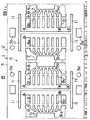
図1は本発明の一実施形態である多連リードフレームを示す一部省略平面図である。図2以降はその多連リードフレームが使用された本発明の一実施形態であるSOP・ICの製造方法の各工程を示す各説明図である。
【0013】
本実施形態において、本発明に係る半導体装置の製造方法は、高密度実装を実現するための半導体集積回路装置(以下、ICという。)である樹脂封止形のSOP・ICを製造するのに使用されている。このSOP・ICの製造方法には、図2に示されている多連リードフレーム1が使用される。この多連リードフレーム1は銅系(銅またはその合金)材料または鉄系(鉄またはその合金)からなる薄板が用いられて、打ち抜きプレス加工またはエッチング加工等の適当な手段により一体成形されており、半田めっき処理は実施されていない。
【0014】
多連リードフレーム1には複数の単位リードフレーム2が横方向に1列に並設されている。但し、連続が理解し得る数単位のみが図示されている。単位リードフレーム2は位置決め孔3aが開設されている外枠3を一対備えており、両外枠3、3は所定の間隔で平行になるように配されて一連にそれぞれ延設されている。隣り合う単位リードフレーム2、2間には一対のセクション枠4が、両外枠3、3間に互いに平行に配されて一体的に架設されており、これら両外枠3、3、両セクション枠4、4によって形成された略長方形の枠体(フレーム)5内に単位リードフレーム2が構成されている。
【0015】
単位リードフレーム2において、両外枠3、3における中央部には一対のタブ吊りリード6、6が直角にそれぞれ突設されており、両タブ吊りリード6、6の先端には長方形の平板形状に形成されたタブ7が、枠体5の枠形状と同心的に配されて一体的に吊持されている。両タブ吊りリード6、6はタブ7に固定される半導体ペレット(以下、ペレットという。)の高さが後記するリード群の一主面と一致するようにそれぞれ屈曲されている。所謂タブ下げである。
【0016】
また、両外枠3、3におけるタブ吊りリード6の両脇には一対のダム部材8、8がそれぞれ架設されており、両ダム部材8、8には複数本のリード9が長手方向に等間隔に配されて、互いに平行でダム部材8と直交するように一体的に突設されている。各リード9におけるダム部材8からタブ7寄りの部分(以下、インナリードという。)9aは、先端がタブ7に近接されて放射状に敷設されている。他方、各リード9の反対側の端部(以下、アウタリードという。)9bは、先端が各セクション枠4に一体的に接続された状態になっている。そして、隣合うアウタリード9b、9b間においてダム部材8は、後述するパッケージ成形時に隣合うアウタリード9b、9b間へのレジンの流れをせき止めるためのダム8aを構成するようになっている。
【0017】
単位リードフレーム2において、隣接する両セクション枠4、4との間には熱応力を緩和するための仕切り用スリット10が両外枠3、3にわたってそれぞれ開設されており、各仕切り用スリット10は一定幅の細長い長孔形状に形成されている。両外枠3、3内における仕切り用スリット10の両端には、仕切り用スリット10と等しい幅の細長い長孔形状のリード成形用スリット11が直角にそれぞれ開設されているとともに、各リード成形用スリット11の先端はダム部材8の延長線の位置よりもタブ吊りリード6の延長線寄りの位置に達している。すなわち、リード成形用スリット11の先端は後記する樹脂封止体の外縁の位置に達しており、この位置はアウタリード9bの屈曲の起点と実質的に等しい位置になるように設定されている。仕切り用スリット10の一端に位置する隣合う単位リードフレーム2、2同士の一対のリード成形用スリット11、11は、互いに一直線に連続した状態になっており、一直線状態になった一対のリード成形用スリット11、11の長さは、隣合う単位リードフレーム2、2のダム部材8、8の間隔よりも若干長くなっている。また、一連となった仕切り用スリット10とリード成形用スリット11群との平面視は「H」が横に寝た形状になっている。
【0018】
このように構成されて準備された多連リードフレーム1には、各単位リードフレーム2毎にペレット・ボンディング作業、続いて、ワイヤ・ボンディング作業が実施され、これら作業により、図2に示されている組立体15が製造されることになる。これらのボンディング作業は多連リードフレームが横方向にピッチ送りされることにより、各単位リードフレーム2毎に順次実施される。また、これらのボンディング作業に際して各単位リードフレーム2は加熱されるが、各単位リードフレーム2毎に仕切り用スリット10が開設されているため、加熱による熱応力は隣の単位リードフレーム2に伝達されることは抑止ないしは緩和され、その結果、多連リードフレーム1が熱応力によって変形することは防止される。
【0019】
まず、ペレットボンディング作業により、前工程において集積回路素子(図示せず)を作り込まれた半導体集積回路構造体としてのペレット13が、各単位リードフレーム2におけるタブ7上の略中央部に配されて、銀ペースト等の適当な材料を用いられて形成されるボンディング層12を介して固着される。銀ペーストは、エポキシ系樹脂接着剤、硬化促進剤、および溶剤に銀粉が混入されて構成されているものであり、リードフレーム上に塗布された銀ペーストにペレットが押接された後、適当な温度によって硬化(キュア)されることにより、ボンディング層12を形成するようになっている。
【0020】
そして、タブ7に固定的にボンディングされたペレット13のボンディングパッド13aと、単位リードフレーム2における各インナリード9aとの間には、銅系材料(銅または銅合金)や金系材料(金または金合金)を使用されて形成されているワイヤ14が、超音波熱圧着式の適当なワイヤボンディング装置が使用されることにより、その両端部をそれぞれボンディングされて橋絡される。以上のボンディング作業により、ペレット13に作り込まれている集積回路は、ボンディングパッド13a、ワイヤ14、インナリード9aおよびアウタリード9bを介して電気的に外部に引き出されることになる。
【0021】
その後、多連リードフレームにペレットおよびワイヤ・ボンディングされた組立体15には樹脂封止体16が、図3に示されているトランスファ成形装置を使用されて単位リードフレーム群について同時成形される。
【0022】
図3に示されているトランスファ成形装置20はシリンダ装置等(図示せず)によって互いに型締めされる上型21と下型22とを備えており、上型21と下型22との合わせ面には長方形の平盤形状の上型キャビティー凹部23aと下型キャビティー凹部23bとが、互いに協働してキャビティー23を形成するようにそれぞれ複数組没設されている。上型21の合わせ面にはポット24が開設されており、ポット24にはシリンダ装置(図示せず)により進退されるプランジャ25が成形材料としての樹脂から成るタブレットが投入され、タブレットが溶融されて成る樹脂(以下、レジンという。)を送給し得るようになっている。
【0023】
下型22の合わせ面にはカル26がポット24との対向位置に配されて没設されているとともに、複数条のランナ27がポット24にそれぞれ接続するように放射状に配されて没設されている。各ランナ27の他端部は下側キャビティー凹部23bにそれぞれ接続されており、その接続部にはゲート28がレジンをキャビティー23内に注入し得るように形成されている。また、下型22の合わせ面には逃げ凹所29がリードフレームの厚みを逃げ得るように、多連リードフレーム1の外形よりも若干大きめの長方形で、その厚さと略等しい寸法の一定深さに没設されている。
【0024】
トランスファ成形に際し、トランスファ成形装置20のワークである前記構成に係る組立体15は下型22に没設されている逃げ凹所29内に載置される。この状態において、単位リードフレーム2におけるペレット13およびインナリード9a群がキャビティー23内にそれぞれ収容され、ダム部材8がキャビティー23の縁辺に近接し、アウタリード9b群がキャビティー23の外側で並んだ状態になる。
【0025】
続いて、上型21と下型22とが型締めされ、ポット24からプランジャ25により成形材料としてのレジン30がランナ27およびゲート28を通じて各キャビティー23に送給されてそれぞれ圧入される。キャビティー23内に圧入されたレジン30はその充填に伴って、上型21と下型22との合わせ面間において隣合うリード9、9の間からキャビティー23の外部に漏洩する。しかし、キャビティー23は隣合うリード9、9間においてダム8a群により包囲されているため、キャビティー23から漏洩したレジン30がダム8aを越えてさらに外方へ流出することはない。そして、キャビティー23から隣合うリード9、9およびダム8aによって取り囲まれた隙間内に漏洩したレジン30により、ダム樹脂ばり(図示せず)が形成されることになる。
【0026】
注入後、レジンが熱硬化されて樹脂封止体16が成形されると、上型21および下型22は型開きされるとともに、エジェクタ・ピン(図示せず)により樹脂封止体16が離型される。このようにして、組立体15に樹脂封止体16を成形された図4に示されている成形体17が製造されたことになる。
【0027】
以上のようにして製造された成形体17の各樹脂封止体16の内部には、ペレット13、インナリード9aおよびワイヤ14が樹脂封止された状態になる。この状態において、樹脂封止体16における両アウタリード9b、9bとダム8aの内側端辺との空間内に形成されたダム樹脂ばり(図示せず)はきわめて微細であるため、樹脂封止体16に殆ど一体化されており、しかも、微細であるため、外観上もダム樹脂ばりと認識され得ない程度のものになっている。
【0028】
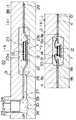
以上のようにして多連リードフレームに樹脂封止体を成形された成形体17は半田めっき処理工程を経る前に、隣合うアウタリード9b、9b間に架設された各ダム8aおよび樹脂ばりを切り落とされる。続いて、図5に示されているように、リード成形装置31が使用されて、成形体17のアウタリード9b群が図6に示されているガルウイング形状に屈曲成形される。次に、図5および図6を参照にして、リード成形工程を説明する。
【0029】
図5に示されているリード成形装置31は上側取付板32、下側取付板33を備えており、上側取付板32はシリンダ装置(図示せず)によって上下動されることにより機台上に固設された下側取付板33に対して接近、離反するように構成されている。上側取付板32および下側取付板33には上側ホルダ34および下側ホルダ35がそれぞれ固定的に取り付けられており、上側ホルダ34および下側ホルダ35には上側押さえ型(以下、上型という。)36および下側押さえ型(以下、下型という。)37が互いに心合わせされてそれぞれ保持されている。上型36および下型37は互いに最中合わせの状態になる略チャンネル型鋼形状にそれぞれ形成されている。上型36および下型37には上側押さえ部38および下側押さえ部39が対称形にそれぞれ形成されており、上側押さえ部38および下側押さえ部39は成形体17の単位リードフレーム2におけるアウタリード9bの根元部を上下から押さえるように構成されている。上型36はガイド40およびスプリング41により独立懸架されている。
【0030】
上側ホルダ34には左右で一対のパンチ42が上型36の左右両脇においてアウタリード9b群の全幅に対応するようにそれぞれ取り付けられており、両パンチ42、42はカム装置によって垂直面内において二次元的に操作されることによりダイと協働して、アウタリード9b群および両外枠3、3の一部(後述する。)をしごき状態なしにガルウイング形状に屈曲成形し得るように構成されている。他方、下型37には左右で一対のダイ43、43が下側押さえ部39の左右両脇に一体的にそれぞれ形成されており、両ダイ43、43はパンチ42と協働してアウタリード9b群および両外枠3、3の一部をガルウイング形状に屈曲成形し得るように構成されている。
【0031】
アウタリード9b群のリード成形に際して、図5(a)に示されているように、下側ホルダ35の上に成形体17が樹脂封止体16を下型37の凹部に落とし込まれるようにしてセットされる。これにより、アウタリード9b群の根元部および両外枠3、3の外側端辺部分が下型37の両下側押さえ部39、39にそれぞれ当接する。
【0032】
次に、シリンダ装置によって上側取付板32が下降され、図5(b)の左半分に示されているように、上型36が下型37にスプリング41の弾発力により合わせられる。これにより、上型36の両上側押さえ部38、38と下型37の両下側押さえ部39、39との間で、被屈曲部としてのアウタリード9b群の根元部および両外枠3、3におけるリード成形用スリット11の外側部分がそれぞれ挟圧されて固定される。
【0033】
続いて、上側取付板32がさらに下降されて行くと、スプリング41が圧縮変形されることにより、パンチ42が下降されて行き、図5(b)の右半分に示されているように、アウタリード9b群、両外枠3、3および両セクション枠4、4のリード成形用スリット11の外側部分はパンチ42の下降に伴ってダイ43に押し付けられることにより、ダイ43に倣うように屈曲されて所望のガルウイング形状に成形される。このとき、パンチ42はカム装置によって外側から内側に向けて斜め下向きに揺動されてアウタリード9b群等を屈曲させるため、アウタリード9b群等にしごき力が作用することはない。したがって、樹脂封止体16とアウタリード9bとの界面が屈曲成形力によって押し開かれる力は作用しない。このため、アウタリード9b群のガルウイング形状の屈曲成形に際して、樹脂封止体16とアウタリード9bとの界面に隙間が発生する現象は防止されることになる。
【0034】
パンチ42が所定のストロークを終了すると、パンチ42は上側取付板32によって上昇され、元の待機状態まで戻される。その後、リード成形済の単位リードフレーム2は下型37から取り外され、次の単位リードフレーム2が下型37にセットされる。以降、前記作動が繰り返されることにより、成形体17の各単位リードフレーム2におけるアウタリード9bについてリード成形が順次実施されて行く。
【0035】
以上のようにして屈曲成形されたリード成形体18は、図6に示されている状態になっている。すなわち、両外枠3、3における両リード成形用スリット11、11の内寄りの端部3bはそれぞれガルウイング形状に屈曲成形されており、屈曲された端部3bの下がった先端間にはセクション枠4が架橋された状態になっている。そして、ガルウイング形状に屈曲成形されて下がった状態になった各アウタリード9bの先端は、下がった状態になったセクション枠4の内側端辺にそれぞれ一体的に連結された状態になっている。
【0036】
その後、リード成形体18は半田めっき処理工程において半田めっき処理を実施される。例えば、図7(a)に示されているように、リード成形体18は半田めっき処理液51に浸漬された状態で、半田めっき処理液51との間に電源装置52によって電圧を印加される。この半田めっき処理によって、多連リードフレーム1には図7(b)に示されているように全体的に半田めっき被膜53が被着される。この際、各アウタリード9bの先端がセクション枠4に一体的に連結されていることにより、各アウタリード9bは全体的に均一に所定の電位になるため、半田めっき被膜53は全体的に均一に被着された状態になる。
【0037】
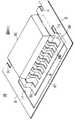
以上のようにして半田めっき処理が実施された後に、多連リードフレーム1の両外枠3、3および両セクション枠4、4がタブ吊りリード6の根元部および各アウタリード9bの先端部において切断されて切り落とされる。これにより、図8に示されているSOP・IC19が製造されたことになる。
【0038】
前記実施形態によれば次の効果が得られる。
(1) リードフレームの枠体のリード群の先端から離れた位置に仕切り用スリットをリード先端群の並び方向と平行に開設し、仕切り用スリットの両端には一対のリード成形用スリットを直角に開設するとともに、各リード成形用スリットの先端をリードの屈曲の起点と実質的に等しい位置に延設することにより、リード成形工程において、リードフレームの各リードにおける樹脂封止体の外側部分を屈曲するに際して、リード成形用スリットの先端部を屈曲点としてリード群の先端を枠体に一体的に連結した状態で屈曲成形することができるため、リード成形後にリードフレームに半田めっき処理を実施しても各リード全体に半田めっき被膜を均一に被着させることができる。
【0039】
(2) 半田めっき被膜をリード成形後に被着することにより、リード成形作業によって半田めっき被膜が損傷されたり、剥離された半田めっき被膜がリードに付着する現象を必然的に回避することができるため、SOP・ICの品質および信頼性を高めることができる。
【0040】
(3) また、半田めっき被膜をリード成形後に被着することにより、リード成形作業においてリード成形装置のパンチやダイに剥離された半田めっき被膜の屑が付着するのを必然的に回避することができるため、半田めっき被膜屑の付着によるリード成形時の所謂打痕不良を防止することができる。
【0041】
以上本発明者によってなされた発明を実施形態に基づき具体的に説明したが、本発明は前記実施形態に限定されるものではなく、その要旨を逸脱しない範囲で種々変更可能であることはいうまでもない。
【0042】
例えば、図9に示されているように、複数の多連リードフレームが多列に連結された多連多列リードフレーム(マルチリードフレーム)1Aにも適用することができる。本実施形態においては、仕切り用スリット10は多列リードフレーム全体を横断するように開設されており、その仕切り用スリット10の両端にリード成形用スリット11が直角にそれぞれ開設されている。
【0043】
リード成形用スリット11は隣合う単位リードフレーム2、2を仕切る一本の仕切り用スリット10の両端に直交するように配設するに限らず、単位リードフレーム2毎に仕切り用スリット10がそれぞれ開設されている場合には、各仕切り用スリット10の両端にそれぞれ直角に配設すればよい。すなわち、仕切り用スリット10と一対のリード成形用スリット11、11とが「コ」字形状に組まれた状態で、各単位リードフレーム2のセクション枠4および両外枠3、3に開設してもよい。
【0044】
半田被膜はアウタリードに半田めっき処理によって被着するに限らず、半田ディップ処理等によって被着してもよい。また、被膜は半田被膜に限らず、錫めっき被膜等のような他の材質の被膜であってもよい。
【0045】
リードフレームにペレットを機械的に接続するとともに各インナリードに電気的に接続する工程や、樹脂封止体を成形する工程、アウタリードを屈曲成形する工程および半田被膜をアウタリードに被着する工程は、前記実施形態の方法および装置を使用して実施するに限られない。
【0046】
以上の説明では主として本発明者によってなされた発明をその背景となった利用分野である樹脂封止SOP・ICの製造方法に適用した場合について説明したが、それに限定されるものではなく、Iリーリッド形状等のようなガルウイング形状以外の形状のアウタリードの樹脂封止パッケージおよび気密封止パッケージを備えているICやトランジスタ等の半導体装置の製造方法全般に適用することができる。
【0047】
【発明の効果】
本願において開示される発明のうち代表的なものによって得られる効果を簡単に説明すれば、次の通りである。
【0048】
リードフレームの枠体のリード群の先端から離れた位置に仕切り用スリットをリード先端群の並び方向と平行に開設し、仕切り用スリットの両端には一対のリード成形用スリットを直角に開設するとともに、各リード成形用スリットの先端をリードの屈曲の起点と実質的に等しい位置に延設することにより、リード成形工程において、リードフレームの各リードにおける封止体の外側部分を屈曲するに際して、リード成形用スリットの先端部を屈曲点としてリード群の先端を枠体に一体的に連結した状態で屈曲成形することができるため、リード成形後にリードフレームに被膜処理を実施しても各リード全体に被膜を均一に被着させることができる。
【0049】
被膜をリード成形後に被着することにより、リード成形作業によって被膜が損傷されたり剥離された被膜がリードに付着する現象を必然的に回避することができるため、半導体装置の品質および信頼性を高めることができる。
【0050】
また、被膜をリード成形後に被着することにより、リード成形作業においてリード成形装置のパンチやダイに剥離された被膜の屑が付着するのを必然的に回避することができるため、被膜屑の付着によるリード成形時の所謂打痕不良を防止することができる。
【図面の簡単な説明】
【図1】本発明の一実施形態である多連リードフレームを示す一部省略平面図である。
【図2】その多連リードフレームが使用された本発明の一実施形態であるSOP・ICの製造方法におけるペレットおよびワイヤボンディング後を示しており、(a)は一部省略平面図、(b)はその正面断面図である。
【図3】その樹脂封止体成形工程を示しており、(a)は一部省略縦断面図、(b)は(a)のb−b線に沿う部分断面図である。
【図4】樹脂封止体成形後の成形体を示しており、(a)は一部省略一部切断平面図、(b)はその正面断面図である。
【図5】(a)、(b)はリード成形工程を示す各一部切断正面図である。
【図6】リード成形後を示す一部省略斜視図である。
【図7】(a)は半田めっき処理工程を示す模式図であり、(b)は半田めっき処理後を示す一部省略斜視図である。
【図8】SOP・ICを示す斜視図である。
【図9】本発明の他の実施形態である多連多列リードフレームの樹脂封止体成形後を示す一部省略平面図である。
【符号の説明】
1…多連リードフレーム、2…単位リードフレーム、3…外枠、3a…位置決め孔、3b…被屈曲端部、4…セクション枠、5…枠体(フレーム)、6…タブ吊りリード、7…タブ、8…ダム部材、8a…ダム、9…リード、9a…インナリード、9b…アウタリード、10…仕切り用スリット、11…リード成形用スリット、12…ボンディング層、13…ペレット、13a…ボンディングパッド、14…ワイヤ、15…組立体、16…樹脂封止体、17…成形体、18…リード成形体、19…SOP・IC(半導体装置)、20…トランスファ成形装置、21…上型、22…下型、23…キャビティー、23a…上型キャビティー凹部、23b…下型キャビティー凹部、24…ポット、25…プランジャ、26…カル、27…ランナ、28…ゲート、29…逃げ凹所、30…レジン、31…リード成形装置、32…上側取付板、33…下側取付板、34…上側ホルダ、35…下側ホルダ、36…上側押さえ型(上型)、37…下側押さえ型(下型)、38…上側押さえ部、39…下側押さえ部、40…ガイド、41…スプリング、42…パンチ、43…ダイ、51…半田めっき処理液、52…電源装置、53…半田めっき被膜(被膜)、1A…多連多列リードフレーム。[0001]
BACKGROUND OF THE INVENTION
The present invention relates to a manufacturing technique of a semiconductor device, and more particularly to a manufacturing technique of a semiconductor device using a lead frame, for example, a semiconductor integrated circuit device (hereinafter referred to as SOP / IC) having a resin-encapsulated small outline package. The present invention relates to a method for manufacturing a semiconductor device effective for use in manufacturing.
[0002]
[Prior art]
In general, a SOP / IC manufacturing method uses a multiple lead frame in which a large number of unit lead frames are connected to each other. The unit lead frame includes a tab for fixing the semiconductor pellet, a plurality of leads arranged radially around the tab, and a frame (frame) for supporting the lead. The unit lead frames are connected to a pair of section frames of a rectangular frame, and adjacent unit lead frames are integrally connected by integrally connecting the frames.
[0003]
In the multiple lead frame, in the pellet and wire bonding step, the semiconductor pellet is bonded to the tab of each unit lead frame, and the wire is bridged between the semiconductor pellet and each lead. Next, in the resin sealing body molding process, the multiple lead frames are housed in the rectangular cavities of the molding die in the molding die of the transfer molding device, and the lead groups penetrate the pair of long sides of the cavity, respectively. After being set in such a manner, a molding material is injected into the cavity, thereby molding a resin sealing body that seals the semiconductor pellet and a part of the lead (hereinafter also referred to as an inner lead). .
[0004]
The multiple lead frame formed with the resin sealing body in this way is subjected to solder plating treatment after removing the dam and the resin burrs in the dam, and then the outer portion of the resin sealing body of each lead (hereinafter, Is sometimes bent into a gull wing shape.
[0005]
An example of a resin-sealed package is “VLSI packaging technology (above)” issued by Nikkei BP Co., Ltd., issued May 31, 1993, P130 to P135.
[0006]
[Problems to be solved by the invention]
In the conventional SOP / IC manufacturing method described above, since the outer lead is bent into a gull wing shape after the solder plating process is performed, the following problems occur. That is, the solder plating film applied to the outer lead is damaged by peeling or cracking when the outer lead is bent. If the scraps of the peeled solder plating film adhere between the outer leads, a short circuit failure or the like is caused as a conductive foreign matter. Further, the outer lead whose solder plating film is damaged becomes poor in appearance due to the exposed base. Further, if the scrap of the solder plating film adheres to the punch or die of the lead forming apparatus, a so-called dent defect is caused at the next lead forming.
[0007]
An object of the present invention is to provide a lead frame that can be subjected to solder plating after lead molding and a method for manufacturing a semiconductor device.
[0008]
The above and other objects and novel features of the present invention will be apparent from the description of this specification and the accompanying drawings.
[0009]
[Means for Solving the Problems]
An outline of typical inventions among inventions disclosed in the present application will be described as follows.
[0010]
That is, a partitioning slit is opened in parallel with the direction in which the lead tip group is arranged at a position away from the tip of the lead group of the lead frame frame, and a pair of lead forming slits are provided at both ends of the partitioning slit. The leads are formed at right angles, and the tip of each lead molding slit extends to a position substantially equal to the starting point of bending of the lead.
[0011]
In the connecting step, the semiconductor pellet is mechanically connected to the lead frame, and the semiconductor pellet is electrically connected to each lead. Subsequently, in a sealing body forming step, a sealing body for sealing the semiconductor pellet and a part of each lead is formed on the lead frame. Next, in the lead molding process, the outer portion of the sealing body in each lead of the lead frame is bent. Thereafter, a film is formed on the surface of the lead frame.
[0012]
DETAILED DESCRIPTION OF THE INVENTION
FIG. 1 is a partially omitted plan view showing a multiple lead frame according to an embodiment of the present invention. FIG. 2 and subsequent figures are explanatory views showing respective steps of the manufacturing method of the SOP / IC which is an embodiment of the present invention in which the multiple lead frame is used.
[0013]
In this embodiment, a method for manufacturing a semiconductor device according to the present invention is used to manufacture a resin-encapsulated SOP / IC that is a semiconductor integrated circuit device (hereinafter referred to as an IC) for realizing high-density mounting. in use. In this SOP / IC manufacturing method, a
[0014]
In the
[0015]
In the
[0016]
A pair of
[0017]
In the
[0018]
The multiple
[0019]
First, a
[0020]
Between the bonding pad 13a of the
[0021]
Thereafter, the
[0022]
The
[0023]
On the mating surface of the
[0024]
At the time of transfer molding, the
[0025]
Subsequently, the
[0026]
After the injection, when the resin is thermoset and the
[0027]
The
[0028]
As described above, the molded
[0029]
The
[0030]
A pair of left and
[0031]
When the
[0032]
Next, the upper mounting
[0033]
Subsequently, when the upper mounting
[0034]
When the
[0035]
The lead molded
[0036]
Thereafter, the lead compact 18 is subjected to a solder plating process in a solder plating process. For example, as shown in FIG. 7A, a voltage is applied by the power supply device 52 between the lead molded
[0037]
After the solder plating process is performed as described above, the
[0038]
According to the embodiment, the following effects can be obtained.
(1) A partitioning slit is opened parallel to the alignment direction of the lead tip group at a position away from the tip of the lead group of the lead frame body, and a pair of lead molding slits are perpendicular to both ends of the partitioning slit. At the same time, by extending the tip of each lead molding slit to a position substantially equal to the starting point of bending of the lead, the outer portion of the resin encapsulant in each lead of the lead frame is bent in the lead molding process. In this case, the lead frame can be bent and molded with the tip of the lead molding slit as the bending point and the tip of the lead group is integrally connected to the frame. Also, the solder plating film can be uniformly applied to the entire leads.
[0039]
(2) By applying the solder plating film after lead molding, it is possible to inevitably avoid the phenomenon that the solder plating film is damaged by the lead molding operation or the peeled solder plating film adheres to the lead. The quality and reliability of the SOP / IC can be improved.
[0040]
(3) Further, by depositing the solder plating film after lead molding, it is inevitably avoided that the solder plating film scraps peeled off from the punch or die of the lead molding apparatus in the lead molding operation. Therefore, a so-called dent defect at the time of lead molding due to adhesion of solder plating film scraps can be prevented.
[0041]
Although the invention made by the present inventor has been specifically described based on the embodiments, the present invention is not limited to the above embodiments, and various modifications can be made without departing from the scope of the invention. Nor.
[0042]
For example, as shown in FIG. 9, the present invention can also be applied to a multiple-multi-row lead frame (multi-lead frame) 1A in which a plurality of multi-lead frames are connected in multiple rows. In this embodiment, the partition slits 10 are opened so as to cross the entire multi-row lead frame, and lead molding slits 11 are opened at right angles at both ends of the partition slits 10.
[0043]
The
[0044]
The solder coating is not limited to being applied to the outer lead by a solder plating process, but may be applied by a solder dipping process or the like. Further, the coating is not limited to a solder coating, and may be a coating made of another material such as a tin plating coating.
[0045]
The steps of mechanically connecting the pellets to the lead frame and electrically connecting to each inner lead, the step of molding the resin sealing body, the step of bending the outer lead, and the step of depositing the solder coating on the outer lead, It is not limited to using the method and apparatus of the above embodiment.
[0046]
In the above description, the case where the invention made by the present inventor is mainly applied to the method of manufacturing the resin-encapsulated SOP / IC, which is the field of use behind it, has been described. However, the present invention is not limited to this. The present invention can be applied to all methods of manufacturing semiconductor devices such as ICs and transistors having an outer lead resin-sealed package and a hermetically sealed package other than a gull-wing shape such as a shape.
[0047]
【The invention's effect】
The effects obtained by the representative ones of the inventions disclosed in the present application will be briefly described as follows.
[0048]
In the lead frame frame, a partition slit is opened parallel to the direction in which the lead tip group is arranged at a position away from the tip of the lead group, and a pair of lead forming slits are opened at both ends of the partition slit at right angles. By extending the tip of each lead molding slit to a position substantially equal to the starting point of bending of the lead, in the lead molding process, when the outer portion of the sealing body in each lead of the lead frame is bent, the lead Bending can be done with the tip of the molding slit at the bending point and the tip of the lead group is integrally connected to the frame. The coating can be applied uniformly.
[0049]
By applying the coating after lead molding, it is possible to inevitably avoid the phenomenon that the coating is damaged or peeled off by the lead molding operation, thereby improving the quality and reliability of the semiconductor device. be able to.
[0050]
In addition, by depositing the coating after lead molding, it is possible to inevitably avoid the coating scraps from being peeled off on the punch or die of the lead molding device in the lead molding operation. It is possible to prevent a so-called dent defect during lead molding.
[Brief description of the drawings]
FIG. 1 is a partially omitted plan view showing a multiple lead frame according to an embodiment of the present invention.
FIG. 2 shows a pellet and wire bonding in a manufacturing method of an SOP / IC that is an embodiment of the present invention in which the multiple lead frame is used, (a) is a partially omitted plan view, (b) ) Is a front sectional view thereof.
FIGS. 3A and 3B show a resin sealing body molding step, in which FIG. 3A is a partially omitted longitudinal sectional view, and FIG. 3B is a partial sectional view taken along line bb in FIG.
4A and 4B show a molded body after molding of a resin sealing body, in which FIG. 4A is a partially omitted plan view with partial omission, and FIG. 4B is a front sectional view thereof.
FIGS. 5A and 5B are each a partially cut front view showing a lead forming process. FIGS.
FIG. 6 is a partially omitted perspective view showing after lead molding.
FIG. 7A is a schematic view showing a solder plating process, and FIG. 7B is a partially omitted perspective view showing the state after the solder plating process.
FIG. 8 is a perspective view showing an SOP IC.
FIG. 9 is a partially omitted plan view showing a multiple-multi-row lead frame according to another embodiment of the present invention after molding of a resin sealing body.
[Explanation of symbols]
DESCRIPTION OF
Claims (2)
Translated fromJapanese行に配置された複数のセクション枠と、前記外枠とセクション枠とによって囲まれる領域
に形成されたタブおよびタブ吊りリードと、一端が前記タブに近接して放射状に敷設され他端が前記セクション枠に接続された複数のリードとから構成された単位リードフレームを有し、この単位リードフレームが横方向一列に設けられるとともに、縦方向に複数列設
けられた多連多列リードフレームにおいて、
前記縦方向に伸びるセクション枠それぞれに前記列方向全体にわたって設けられた複数の仕切り用スリットと、前記仕切り用スリットそれぞれの両端にある前記縦方向に複数列の単位リードフレームの一番外側の外枠それぞれに、前記仕切り用スリットそれぞれとその先端部で直角に交わり前記仕切り用スリットそれぞれの両側の単位リードフレームそれぞれに延在して設けられた複数の一対のリード成形用スリットとを有しており、
前記複数の一対のリード成形用スリットの一方の先端部それぞれと他方の先端部それぞれとは、前記一対のリード成形用スリットの間に挟まれた前記複数のリードを屈曲して成形する際の屈曲点となることを特徴とする多連多列リードフレーム。Formed in a region surrounded by a pair of outer frames arranged in parallel at a predetermined interval, a plurality of section frames connecting the outer frames and arranged in parallel at a predetermined distance from each other, and the outer frame and the section frame A unit lead frame comprising a tab and a tab suspension lead, and a plurality of leads having one end laid radially adjacent to the tab and the other end connected to the section frame. Are provided in a row in the horizontal direction, and in a multiple-multi-row lead frame provided in a plurality of rows in the vertical direction,
Aplurality of partition slits provided over the entire column direction in each of the section frames extending in the vertical direction, and an outermost outerframe ofthe unit lead frames in theplurality of columns in the vertical direction at both ends of each of the partition slitsrespectively,and have arespective said partition slit and aplurality of pairs of leads molding slits provided extending at right angles to each unit lead frame on both sides ofeach intersection the partition slitat its distal end,
Each of the one end and the other end of each of the plurality of pairs of lead forming slits is bent when the plurality of leads sandwiched between the pair of lead forming slits are formed by bending. A multi-row lead frame characterized by being adot .
定の距離隔てて平行に配置された複数のセクション枠と、前記外枠とセクション枠とによA plurality of section frames arranged in parallel at a predetermined distance, and the outer frame and the section frame.
って囲まれる領域に形成されたタブおよびタブ吊りリードと、一端が前記タブに近接して放射状に敷設され他端が前記セクション枠に接続された複数のリードとから構成された単A tab and a tab suspension lead formed in a region surrounded by a plurality of leads, one end of which is laid radially adjacent to the tab and the other end is connected to the section frame.
位リードフレームを有し、この単位リードフレームが横方向一列に設けられるとともに、The unit lead frame is provided in a row in the horizontal direction,
縦方向に複数列設けられた多連多列リードフレームを用いる半導体装置の製造方法であって、A method of manufacturing a semiconductor device using a multiple-multi-row lead frame provided in a plurality of rows in a vertical direction,
前記縦方向に伸びるセクション枠それぞれに前記列方向全体にわたって設けられた仕切り用スリットと、前記仕切り用スリットそれぞれの両端にある前記多列の一番外側の外枠 Partition slits provided over the entire column direction in each of the section frames extending in the vertical direction, and the outermost outer frame of the multi-row at each end of each of the partition slits
それぞれに前記仕切り用スリットと直角に交わり前記仕切り用スリットの両側の単位リードフレームそれぞれに延在して設けられたリード成形用スリットとを有する多連多列リードフレームを準備する工程、A step of preparing a multiple-row lead frame having lead forming slits each extending perpendicularly to each of the unit lead frames on both sides of the partition slit;
前記多連多列リードフレームの前記各タブに半導体ペレットを接続する工程、 Connecting semiconductor pellets to the tabs of the multiple-multi-row lead frame;
前記半導体ペレットと前記複数のリードとを接続する工程、 Connecting the semiconductor pellet and the plurality of leads;
前記各半導体ペレットと複数のリードの一部とを樹脂によって封止する工程、 Sealing each of the semiconductor pellets and a plurality of leads with a resin;
前記縦方向の前記セクション枠によって囲まれる複数の単位リードフレームそれぞれの封止樹脂から突出するリードを、前記仕切り用スリットおよび前記リード成形用スリットによって囲まれる前記セクション枠と共に、ガルウィング形状に屈曲成形する工程、 A lead protruding from the sealing resin of each of the plurality of unit lead frames surrounded by the section frame in the vertical direction is bent and formed into a gull wing shape together with the section frame surrounded by the partition slit and the lead molding slit. Process,
前記屈曲成形後の前記多連多列リードフレームをめっき処理する工程、 A step of plating the multiple multi-row lead frame after the bending molding;
を有することを特徴とする半導体装置の製造方法。 A method for manufacturing a semiconductor device, comprising:
Priority Applications (1)
| Application Number | Priority Date | Filing Date | Title |
|---|---|---|---|
| JP15026596AJP3617574B2 (en) | 1996-05-22 | 1996-05-22 | Multiple-multi-row lead frame and method of manufacturing semiconductor device using the same |
Applications Claiming Priority (1)
| Application Number | Priority Date | Filing Date | Title |
|---|---|---|---|
| JP15026596AJP3617574B2 (en) | 1996-05-22 | 1996-05-22 | Multiple-multi-row lead frame and method of manufacturing semiconductor device using the same |
Publications (2)
| Publication Number | Publication Date |
|---|---|
| JPH09312368A JPH09312368A (en) | 1997-12-02 |
| JP3617574B2true JP3617574B2 (en) | 2005-02-09 |
Family
ID=15493169
Family Applications (1)
| Application Number | Title | Priority Date | Filing Date |
|---|---|---|---|
| JP15026596AExpired - Fee RelatedJP3617574B2 (en) | 1996-05-22 | 1996-05-22 | Multiple-multi-row lead frame and method of manufacturing semiconductor device using the same |
Country Status (1)
| Country | Link |
|---|---|
| JP (1) | JP3617574B2 (en) |
Families Citing this family (2)
| Publication number | Priority date | Publication date | Assignee | Title |
|---|---|---|---|---|
| JP3085278B2 (en) | 1998-05-01 | 2000-09-04 | 日本電気株式会社 | Semiconductor device manufacturing method and semiconductor manufacturing apparatus |
| CN113414314B (en)* | 2021-08-24 | 2021-11-19 | 常州协和光电器件有限公司 | Line folding machine for circuit board assembly and working method thereof |
- 1996
- 1996-05-22JPJP15026596Apatent/JP3617574B2/ennot_activeExpired - Fee Related
Also Published As
| Publication number | Publication date |
|---|---|
| JPH09312368A (en) | 1997-12-02 |
Similar Documents
| Publication | Publication Date | Title |
|---|---|---|
| US6861734B2 (en) | Resin-molded semiconductor device | |
| US7410834B2 (en) | Method of manufacturing a semiconductor device | |
| JP2972096B2 (en) | Resin-sealed semiconductor device | |
| JPS61125062A (en) | Method and device for attaching pin | |
| JPH11260985A (en) | Lead frame, resin-sealed semiconductor device and its manufacture | |
| JP2003158234A (en) | Semiconductor device and manufacturing method thereof | |
| JP3617574B2 (en) | Multiple-multi-row lead frame and method of manufacturing semiconductor device using the same | |
| JPH10256460A (en) | Terminal land frame, resin sealed type semiconductor device using it, and manufacture of the device | |
| JP3025093B2 (en) | Semiconductor device and its mounting structure | |
| JP2886250B2 (en) | Semiconductor device | |
| JP2002100722A (en) | Semiconductor device | |
| JP2000012756A (en) | Semiconductor device, method of manufacturing the same, and mounting structure using the same | |
| JP3501935B2 (en) | Method for manufacturing semiconductor device | |
| JP4266429B2 (en) | Resin-sealed semiconductor device and manufacturing method thereof | |
| JP3747991B2 (en) | Manufacturing method of semiconductor device | |
| JP3986189B2 (en) | Manufacturing method of semiconductor device | |
| JP3127104B2 (en) | Mold for sealing resin-encapsulated semiconductor device and manufacturing method using the same | |
| JPH09129661A (en) | Molding apparatus and molding method | |
| JPH01123448A (en) | Manufacturing method of semiconductor device | |
| JPH07142645A (en) | Semiconductor device and manufacturing method thereof | |
| JPH09312371A (en) | Semiconductor device, manufacturing method thereof, and lead frame used for the same | |
| JPH06244349A (en) | Semiconductor device, manufacturing method for it, and lead frame | |
| JP2004104155A (en) | Semiconductor device | |
| JPH09223770A (en) | Semiconductor device, method of manufacturing the same, and lead frame used for manufacturing the same | |
| JPH06177313A (en) | Semiconductor device and its manufacture and lead frame used in the same |
Legal Events
| Date | Code | Title | Description |
|---|---|---|---|
| A131 | Notification of reasons for refusal | Free format text:JAPANESE INTERMEDIATE CODE: A131 Effective date:20040203 | |
| A521 | Written amendment | Free format text:JAPANESE INTERMEDIATE CODE: A523 Effective date:20040402 | |
| A131 | Notification of reasons for refusal | Free format text:JAPANESE INTERMEDIATE CODE: A131 Effective date:20040608 | |
| A521 | Written amendment | Free format text:JAPANESE INTERMEDIATE CODE: A523 Effective date:20040805 | |
| TRDD | Decision of grant or rejection written | ||
| A01 | Written decision to grant a patent or to grant a registration (utility model) | Free format text:JAPANESE INTERMEDIATE CODE: A01 Effective date:20041102 | |
| A61 | First payment of annual fees (during grant procedure) | Free format text:JAPANESE INTERMEDIATE CODE: A61 Effective date:20041102 | |
| R150 | Certificate of patent or registration of utility model | Free format text:JAPANESE INTERMEDIATE CODE: R150 | |
| FPAY | Renewal fee payment (event date is renewal date of database) | Free format text:PAYMENT UNTIL: 20071119 Year of fee payment:3 | |
| FPAY | Renewal fee payment (event date is renewal date of database) | Free format text:PAYMENT UNTIL: 20081119 Year of fee payment:4 | |
| FPAY | Renewal fee payment (event date is renewal date of database) | Free format text:PAYMENT UNTIL: 20081119 Year of fee payment:4 | |
| FPAY | Renewal fee payment (event date is renewal date of database) | Free format text:PAYMENT UNTIL: 20091119 Year of fee payment:5 | |
| FPAY | Renewal fee payment (event date is renewal date of database) | Free format text:PAYMENT UNTIL: 20101119 Year of fee payment:6 | |
| FPAY | Renewal fee payment (event date is renewal date of database) | Free format text:PAYMENT UNTIL: 20111119 Year of fee payment:7 | |
| FPAY | Renewal fee payment (event date is renewal date of database) | Free format text:PAYMENT UNTIL: 20111119 Year of fee payment:7 | |
| S111 | Request for change of ownership or part of ownership | Free format text:JAPANESE INTERMEDIATE CODE: R313111 | |
| FPAY | Renewal fee payment (event date is renewal date of database) | Free format text:PAYMENT UNTIL: 20111119 Year of fee payment:7 | |
| R350 | Written notification of registration of transfer | Free format text:JAPANESE INTERMEDIATE CODE: R350 | |
| FPAY | Renewal fee payment (event date is renewal date of database) | Free format text:PAYMENT UNTIL: 20111119 Year of fee payment:7 | |
| FPAY | Renewal fee payment (event date is renewal date of database) | Free format text:PAYMENT UNTIL: 20121119 Year of fee payment:8 | |
| LAPS | Cancellation because of no payment of annual fees |