JP3615919B2 - Plasma CVD equipment - Google Patents
Plasma CVD equipmentDownload PDFInfo
- Publication number
- JP3615919B2 JP3615919B2JP30878997AJP30878997AJP3615919B2JP 3615919 B2JP3615919 B2JP 3615919B2JP 30878997 AJP30878997 AJP 30878997AJP 30878997 AJP30878997 AJP 30878997AJP 3615919 B2JP3615919 B2JP 3615919B2
- Authority
- JP
- Japan
- Prior art keywords
- electrode
- potential control
- potential
- film
- reaction vessel
- Prior art date
- Legal status (The legal status is an assumption and is not a legal conclusion. Google has not performed a legal analysis and makes no representation as to the accuracy of the status listed.)
- Expired - Fee Related
Links
- 238000005268plasma chemical vapour depositionMethods0.000titleclaimsdescription21
- 238000010438heat treatmentMethods0.000claimsdescription7
- 238000007599dischargingMethods0.000claimsdescription6
- 239000002994raw materialSubstances0.000claimsdescription6
- 239000012528membraneSubstances0.000claims1
- 239000010408filmSubstances0.000description51
- 239000000758substrateSubstances0.000description26
- 239000007789gasSubstances0.000description19
- 229910021424microcrystalline siliconInorganic materials0.000description11
- 239000010409thin filmSubstances0.000description8
- 230000015572biosynthetic processEffects0.000description6
- 239000012212insulatorSubstances0.000description5
- 238000000151depositionMethods0.000description4
- 230000008021depositionEffects0.000description4
- 238000010586diagramMethods0.000description4
- 230000000694effectsEffects0.000description4
- 238000001069Raman spectroscopyMethods0.000description3
- 239000011521glassSubstances0.000description3
- 238000010849ion bombardmentMethods0.000description3
- UFHFLCQGNIYNRP-UHFFFAOYSA-NHydrogenChemical compound[H][H]UFHFLCQGNIYNRP-UHFFFAOYSA-N0.000description2
- BLRPTPMANUNPDV-UHFFFAOYSA-NSilaneChemical compound[SiH4]BLRPTPMANUNPDV-UHFFFAOYSA-N0.000description2
- 229910021417amorphous siliconInorganic materials0.000description2
- 239000000463materialSubstances0.000description2
- 238000005259measurementMethods0.000description2
- 238000000034methodMethods0.000description2
- 239000013081microcrystalSubstances0.000description2
- 239000012495reaction gasSubstances0.000description2
- 238000001228spectrumMethods0.000description2
- 229910000577Silicon-germaniumInorganic materials0.000description1
- 239000000470constituentSubstances0.000description1
- 239000013078crystalSubstances0.000description1
- 229910021419crystalline siliconInorganic materials0.000description1
- 239000003599detergentSubstances0.000description1
- 229910003460diamondInorganic materials0.000description1
- 239000010432diamondSubstances0.000description1
- 230000004907fluxEffects0.000description1
- 239000001257hydrogenSubstances0.000description1
- 229910052739hydrogenInorganic materials0.000description1
- 150000002500ionsChemical class0.000description1
- 230000007935neutral effectEffects0.000description1
- 239000003960organic solventSubstances0.000description1
- 230000000087stabilizing effectEffects0.000description1
Images


Classifications
- Y—GENERAL TAGGING OF NEW TECHNOLOGICAL DEVELOPMENTS; GENERAL TAGGING OF CROSS-SECTIONAL TECHNOLOGIES SPANNING OVER SEVERAL SECTIONS OF THE IPC; TECHNICAL SUBJECTS COVERED BY FORMER USPC CROSS-REFERENCE ART COLLECTIONS [XRACs] AND DIGESTS
- Y02—TECHNOLOGIES OR APPLICATIONS FOR MITIGATION OR ADAPTATION AGAINST CLIMATE CHANGE
- Y02E—REDUCTION OF GREENHOUSE GAS [GHG] EMISSIONS, RELATED TO ENERGY GENERATION, TRANSMISSION OR DISTRIBUTION
- Y02E10/00—Energy generation through renewable energy sources
- Y02E10/50—Photovoltaic [PV] energy
Landscapes
- Chemical Vapour Deposition (AREA)
- Photovoltaic Devices (AREA)
Description
Translated fromJapanese【0001】
【発明の属する技術分野】
本発明はプラズマCVD装置に関し、特にプラズマCVD法を用いた微結晶及び多結晶系薄膜を製造するプラズマCVD装置に関する。
【0002】
【従来の技術】
膜中に数nm〜数百nmの結晶粒を有する所謂微結晶薄膜はアモルファス系の薄膜に対して電気的特性が優れる、経時的に安定である等の理由から、次世代の太陽電池やTFT(Thin Film Transistor )などの材料として注目されている。微結晶膜は大面積化が容易、比較的低温で形成できる等の理由からプラズマCVD法を用いて製作するのが一般的である。図4は、従来の典型的なプラズマCVD装置の基本構成図を示す。
【0003】
図中の符番1は真空チャンバを示す。この真空チャンバ1内には、基板2を加熱する機能を有した基板加熱ヒータ3が配置されている。前記真空チャンバ1内には、プラズマを生成するための電極4が基板2と対向するように配置されている。前記電極4は、電気的に接地された成膜ユニット5に図示しない絶縁碍子を介して固定されている。前記電極4には、高周波電源6より電力導入端子7を介してプラズマ生成用の電力が供給される。前記高周波電源6と電力導入端子7には、電極4と高周波電源6のインピーダンス整合をとるためのインピーダンス整合器8が接続されている。前記真空チャンバ1には、前記電極4周辺に原料ガスを導入するガス導入管9、及び真空チャンバ1内の反応ガス等を真空ポンプ(図示せず)により容器外へ排出する排気管10が設けられている。
【0004】
こうした構成の装置を用いて微結晶シリコン膜を成膜するには、原料ガスとして水素ガスで希釈したモノシランガスを所定流量流して、圧力を0.2ないし1Torr程度に調整し、基板温度を160℃ないし250℃程度に設定して高周波電力を電極4に印加し、基板加熱ヒータ3と電極4間にプラズマを発生させ、前述の原料ガスを分解して基板2上に膜を堆積させる。
【0005】
よく知られているように、微結晶シリコン膜を成膜するためには、アモルファスシリコンなどの成膜に比べ高周波電力が数倍〜数十倍必要である。しかしながら、このように高電力を印加した場合、プラズマの電位が増加するので基板2へ入射するイオンのフラックスエネルギーが増大するため、膜表面にイオン衝撃ダメージが増加し、高品質の微結晶シリコン膜を成膜することが困難であった。
【0006】
このため、図5に示すように基板2と電極4の間にメッシュ電極(グリッド電極)11を挿入し、これに直流電源12を接続して負の電圧を印加する方法がある。このようにすると、プラズマがメッシュ電極11と電極4の間に閉じ込められ、基板2とメッシュ電極11の間のプラズが弱くなることから成膜時の基板2へのイオン衝撃を低下することができるので、高品質の微結晶シリコン膜が成膜可能となる。
【0007】
【発明が解決しようとする課題】
しかしながら、この方法ではメッシュ電極11が該メッシュ電極11と電極4の間で生成された膜の基となるラジカルの基板面へ流れを物理的に阻害するため、膜の成長速度が極端に遅くなること、及びメッシュ電極11への膜堆積によるメッシュの閉塞により成膜速度が経時的に低下するという問題があった。
【0008】
本発明はこうした事情を考慮してなされたもので、開口部を有する電極に対して被処理物と反対側に電位制御板を配置し、この電位制御板の電位を電位制御電源により制御する構成とすることにより、電極とヒータ間のプラズマ電位を小さくでき、もって膜の結晶性を向上しえるプラズマCVD装置を提供することを目的とする。
【0009】
又、本発明は、開口部を有する電極に対して被処理物と反対側に被処理物側が開口した成膜ユニットを配置し、この成膜ユニットの電位を電位制御電源により制御する構成とすることにより、電極とヒータ間のプラズマ電位を小さくでき、もって膜の結晶性を向上しえるとともに、プラズマ電位の制御性に優れたプラズマCVD装置を提供することを目的とする。
【0010】
【課題を解決するための手段】
本願第1の発明は、反応容器と、この反応容器に原料ガスを導入、排出する手段と、前記反応容器内に配置され、被処理物を加熱するヒータと、前記反応容器内に配置され、被処理物側に開口部を有した成膜ユニットと、この成膜ユニットの開口部に前記被処理物と対向するようにセットされ、開口部を有する電極と、前記成膜ユニットの被処理物側と反対側に該成膜ユニットと絶縁して配置された電位制御板と、この電位制御板の電位を制御する電位制御電源と、前記電極とヒータ間、前記電極と電位制御板間にプラズマを発生させる手段とを具備することを特徴とするプラズマCVD装置である。
【0011】
本願第2の発明は、反応容器と、この反応容器に原料ガスを導入、排出する手段と、前記反応容器内に配置され、被処理物を加熱するヒータと、前記反応容器内に配置され、被処理物側に開口部を有した成膜ユニットと、この成膜ユニットの開口部に前記被処理物と対向するようにセットされ、開口部を有する電極と、前記成膜ユニットの電位を制御する電位制御電源と、前記電極とヒータ間、前記電極と成膜ユニット間にプラズマを発生させる手段とを具備することを特徴とするプラズマCVD装置である。
【0012】
本発明において、原料を導入する手段としては、図1に示すようなガス導入管が挙げられる。また、原料ガスを排出する手段としては排気管が挙げられる。
本発明において、開口部を有する電極とは、電極主面に垂直な方向にガスを通過させるような穴あるいは隙間を有した電極を意味し、例えば、図1に示すようなラダー(梯子状)電極、あるいは図5で述べたようなグリッド型電極が挙げられる。
【0013】
本発明において、プラズマを発生させる手段としては、例えば図1に示すような高周波電源、インピーダンス整合器及び電力導入端子からなる構成部材が挙げられる。
【0014】
【発明の実施の形態】
以下、本発明の実施例を図面を参照して説明する。
(実施例1)
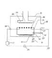
図1を参照する。図中の符番21は、反応容器としての真空チャンバを示す。この真空チャンバ21内には、基板ホルダ(図示せず)に支持されたガラス基板22を加熱する基板加熱ヒータ23が配置されている。ここで、ガラス基板22は中性洗剤あるいは有機溶剤で洗浄したものを用いる。前記真空チャンバ21内には、プラズマを生成するためのラダー電極24が基板22と対向するように配置されている。前記ラダー電極24は、電気的に接地された成膜ユニット25に図示しない絶縁体を介して固定されている。前記ラダー電極24には、高周波電源26より例えば13.56MHzの高周波をインピーダンス整合器27、電力導入端子28を介して印加し、グロー放電プラズマが発生させる。グロー放電プラズマは、基板加熱ヒータ23とラダー電極24の間、及びラダー電極24と後述する電位制御板の間の両方に発生する。前記成膜ユニット25の底部には絶縁碍子29を介して電位制御板30が設けられ、該電位制御板30には電位制御用電源30が接続されている。ここで、電位制御用電源31により電位制御板30の電位が制御される。前記真空チャンバ21には、前記ラダー電極24周辺に原料ガスを導入するガス導入管32、及び真空チャンバ21内の反応ガスなどを真空ポンプ(図示せず)により容器外へ排出する排気管33が設けられている。
【0015】
こうした装置において、真空チャンバ21内は真空ポンプにより所定圧力(通常は5×10⁻⁷Torr以下)まで排気すると共に、基板加熱ヒータ23に通電してガラス基板22を所定温度、通常150℃〜300℃に加熱し、温度を十分安定させた後、真空チャンバ21内にガス導入管32を介して原料ガスとして水素とモノシランの混合ガスを所定流量導入し、真空ポンプによりガス排気管33を介して排出される。
【0016】
上記実施例に係るプラズマCVD装置によれば、ラダー電極24に対して基板22と反対側に電位制御板30を配置し、この電位制御板30の電位を電位制御電源31により制御する構成となっているため、以下に述べる効果を有する。
【0017】
(1) ラダー電極24を構成する線材の隙間を介してラダー電極24と基板加熱ヒータ23間のプラズマとラダー電極24と電位制御板30の間のプラズマがつながっているため、電位制御板30の電位を制御することにより、ラダー電極24と基板加熱ヒータ23間のプラズマ電位を小さくすることが可能となる。この結果、イオン衝撃による膜面へのダメージが低減されることから、膜の結晶性が向上する。
【0018】
(2) 基板22の前面には従来のグリッド電極等のようにラジカルにとって遮蔽物がないことから、成膜速度を損なうことなく結晶性を向上できる。
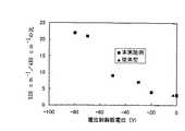
事実、前記プラズマCVD装置を用いて電位制御板30に印加する電圧を変化させ、基板22上に微結晶Si薄膜を成膜した。微結晶Si薄膜の膜厚は50nmとした。成膜した微結晶Si薄膜はレーザラマン分光測定により膜質の評価を行った。測定結果のラマン散乱スペクトルを480cm−1及び520cm−1を中心値とするガウス分布にて波形分布してそのピーク比を調べた。ここで、480cm−1はアモルファスSi成分を示し、520cm−1は結晶Si成分を示すものである。
【0019】
一般的に、その比(520cm−1のピーク値)/(480cm−1のピーク値)が大きいものほど、微結晶Si膜の結晶性が高く且つ高品質膜とされている。電位制御板30に印加する電圧とその時に得られた膜の(520cm−1のピーク値)/(480cm−1のピーク値)の関係は、図2に示す通りであった。また、比較のために従来のプラズマCVD法で製作した微結晶Si膜の値も示した。更に、この時の成膜速度と電位制御板電位との関係を図3に示す。図2及び図3より、成膜速度を落とさずに高品質の微結晶膜が得られることが確認できた。
【0020】
(実施例2)
図6を参照する。但し、図1と同部材は同符号を付して説明を省略する。本実施例2は、実施例1と比べ、電位制御板を省き、代わりに電気的に接地されていた成膜ユニット25に電位制御電源31を接続して成膜ユニット25の電位を制御したものである。前記成膜ユニット25と真空チャンバ21間、成膜ユニット25とガス導入管32間には、夫々板状の絶縁碍子61、断面が環状の絶縁碍子62が設けられている。
【0021】
実施例2に係るプラズマCVD装置によれば、実施例1と同様な効果を有する他、実施例1の電位制御板よりもプラズマに接している面積が大きくなるので、実施例1よりもプラズマ電位の制御性が優れる。
【0022】
なお、上記実施例では、微結晶Siの成膜例を示したが、これに限らず、微結晶SiCや微結晶SiGeなどのSi系微結晶、ダイヤモンド系の微結晶等の成膜に関しても同様に効果がある。
【0023】
また、上記実施例では、電極はラダー電極を用いたが、グリッド型等の開口部があり、電極の上下のプラズマがつながっているような電極では同様の効果が得られる。
【0024】
【発明の効果】
以上詳述したように本発明によれば、開口部を有する電極に対して被処理物と反対側に電位制御板を配置し、この電位制御板の電位を電位制御電源により制御する構成とすることにより、電極とヒータ間のプラズマ電位を小さくでき、もって膜の結晶性を向上しえるプラズマCVD装置を提供できる。
【0025】
また、本発明によれば、開口部を有する電極に対して被処理物と反対側に被処理物側が開口した成膜ユニットを配置し、この成膜ユニットの電位を電位制御電源により制御する構成とすることにより、電極とヒータ間のプラズマ電位を小さくでき、もって膜の結晶性を向上しえるとともに、プラズマ電位の制御性に優れたプラズマCVD装置を提供できる。
【図面の簡単な説明】
【図1】本発明の実施例1に係るプラズマCVD装置の全体図。
【図2】本発明装置及び従来装置による微結晶Si薄膜のラマン散乱スペクトルのピーク比(520cm−1/480cm−1の比)と電位制御板電位との関係を示す特性図。
【図3】本発明による成膜速度と電位制御板電位との関係を示す特性図。
【図4】従来のプラズマCVD装置の説明図。
【図5】従来の他のプラズマCVD装置の説明図。
【図6】本発明の実施例2に係るプラズマCVD装置の全体図。
【符号の説明】
21…真空チャンバ、
22…基板、
23…基板加熱ヒータ、
24…ラダー電極、
25…成膜ユニット、
26…高周波電源、
27…インピーダンス整合器、
28…電力導入端子、
30…電位制御電源、
31…電位制御板、
32…ガス導入管、
33…ガス排気管。[0001]
BACKGROUND OF THE INVENTION
The present invention relates to a plasma CVD apparatus, and more particularly to a plasma CVD apparatus for producing microcrystalline and polycrystalline thin films using a plasma CVD method.
[0002]
[Prior art]
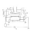
The so-called microcrystalline thin film having crystal grains of several nm to several hundred nm in the film has excellent electrical characteristics compared to the amorphous thin film, and is stable over time. It has been attracting attention as a material such as (Thin Film Transistor). A microcrystalline film is generally manufactured using a plasma CVD method because it can easily be enlarged and formed at a relatively low temperature. FIG. 4 shows a basic configuration diagram of a conventional typical plasma CVD apparatus.
[0003]
Reference numeral 1 in the figure indicates a vacuum chamber. A
[0004]
In order to form a microcrystalline silicon film using an apparatus having such a configuration, a monosilane gas diluted with hydrogen gas is supplied as a source gas at a predetermined flow rate, the pressure is adjusted to about 0.2 to 1 Torr, and the substrate temperature is set to 160 ° C. In addition, a high frequency power is applied to the
[0005]
As is well known, in order to form a microcrystalline silicon film, high frequency power is required several times to several tens of times as compared with the film formation of amorphous silicon or the like. However, when high power is applied in this way, the plasma potential increases, so that the flux energy of ions incident on the substrate 2 increases, resulting in increased ion bombardment damage on the film surface and high quality microcrystalline silicon film. It was difficult to form a film.
[0006]
For this reason, there is a method in which a mesh electrode (grid electrode) 11 is inserted between the substrate 2 and the
[0007]
[Problems to be solved by the invention]
However, in this method, the
[0008]
The present invention has been made in consideration of such circumstances, and a configuration in which a potential control plate is disposed on the side opposite to the object to be processed with respect to an electrode having an opening, and the potential of the potential control plate is controlled by a potential control power source. Thus, it is an object of the present invention to provide a plasma CVD apparatus that can reduce the plasma potential between the electrode and the heater and thereby improve the crystallinity of the film.
[0009]
In the present invention, a film forming unit having an opening on the side opposite to the object to be processed is disposed with respect to the electrode having the opening, and the potential of the film forming unit is controlled by a potential control power source. Accordingly, an object of the present invention is to provide a plasma CVD apparatus which can reduce the plasma potential between the electrode and the heater, thereby improving the crystallinity of the film and having excellent controllability of the plasma potential.
[0010]
[Means for Solving the Problems]
The first invention of the present application is a reaction vessel, a means for introducing and discharging a raw material gas into the reaction vessel, a heater arranged in the reaction vessel and heating an object to be processed, and arranged in the reaction vessel,A film forming unit having an opening on the object to be processed, an electrode set in the opening of the film forming unit so as to face the object to be processed, and having an opening, and anobject to be processed of the film forming unit A potential control plate disposed on theopposite side to the film forming unit, a potential control power source for controlling the potential of the potential control plate, a plasma between the electrode and the heater, and a plasma between the electrode and the potential control plate. And a means for generating the plasma CVD apparatus.
[0011]
The second invention of the present application is a reaction vessel, a means for introducing and discharging a raw material gas into the reaction vessel, a heater arranged in the reaction vessel and heating an object to be processed, and arranged in the reaction vessel,A film forming unit having an openingon the processing object side, an electrode having an opening set in the opening of the film forming unit so as to face the object to be processed, and a potential of the film forming unit are controlled. And a means for generating plasma between the electrode and the heater, and between the electrode and the film forming unit.
[0012]
In the present invention, examples of the means for introducing the raw material include a gas introduction pipe as shown in FIG. An exhaust pipe is an example of means for discharging the source gas.
In the present invention, an electrode having an opening means an electrode having a hole or a gap through which gas passes in a direction perpendicular to the electrode main surface. For example, a ladder (ladder shape) as shown in FIG. An electrode or a grid-type electrode as described in FIG.
[0013]
In the present invention, as means for generating plasma, for example, a constituent member including a high-frequency power source, an impedance matching device, and a power introduction terminal as shown in FIG.
[0014]
DETAILED DESCRIPTION OF THE INVENTION
Embodiments of the present invention will be described below with reference to the drawings.
Example 1
Please refer to FIG.
[0015]
In such an apparatus, the inside of the
[0016]
According to the plasma CVD apparatus according to the above embodiment, the
[0017]
(1) Since the plasma between the
[0018]
(2) Since there is no shielding material for radicals on the front surface of the
In fact, the voltage applied to the
[0019]
In general, the larger the ratio (peak value at 520 cm−1 ) / (peak value at 480 cm−1 ), the higher the crystallinity of the microcrystalline Si film and the higher the quality film. The relationship between the voltage applied to the
[0020]
(Example 2)
Please refer to FIG. However, the same members as those in FIG. In the second embodiment, the potential control plate is omitted, and the potential of the
[0021]
The plasma CVD apparatus according to the second embodiment has the same effect as that of the first embodiment, and also has a larger area in contact with the plasma than the potential control plate of the first embodiment. Excellent controllability.
[0022]
In the above embodiment, an example of film formation of microcrystalline Si is shown. However, the present invention is not limited to this, and the same applies to film formation of Si-based microcrystals such as microcrystalline SiC and microcrystalline SiGe, and diamond-based microcrystals. Is effective.
[0023]
In the above embodiment, a ladder electrode is used. However, the same effect can be obtained with an electrode having a grid-type opening and connecting plasma above and below the electrode.
[0024]
【The invention's effect】
As described above in detail, according to the present invention, a potential control plate is disposed on the opposite side of the workpiece with respect to the electrode having the opening, and the potential of the potential control plate is controlled by the potential control power source. Thus, it is possible to provide a plasma CVD apparatus that can reduce the plasma potential between the electrode and the heater, thereby improving the crystallinity of the film.
[0025]
Further, according to the present invention, a film forming unit having an opening on the side opposite to the object to be processed is disposed on the electrode having the opening, and the potential of the film forming unit is controlled by the potential control power source. Thus, it is possible to reduce the plasma potential between the electrode and the heater, thereby improving the crystallinity of the film and providing a plasma CVD apparatus excellent in controllability of the plasma potential.
[Brief description of the drawings]
FIG. 1 is an overall view of a plasma CVD apparatus according to Embodiment 1 of the present invention.
[2] The present invention apparatus and characteristic diagram showing the relationship of the peak ratio(ratio of 520cm-1 / 480cm -1) the potential control plate potential of the Raman scattering spectrum of the microcrystalline Si thin film by the conventional apparatus.
FIG. 3 is a characteristic diagram showing the relationship between the deposition rate and the potential control plate potential according to the present invention.
FIG. 4 is an explanatory diagram of a conventional plasma CVD apparatus.
FIG. 5 is an explanatory view of another conventional plasma CVD apparatus.
FIG. 6 is an overall view of a plasma CVD apparatus according to Embodiment 2 of the present invention.
[Explanation of symbols]
21 ... Vacuum chamber,
22 ... substrate,
23 ... Substrate heater,
24: Ladder electrode,
25 ... Film formation unit,
26 ... high frequency power supply,
27. Impedance matching device,
28 ... Power introduction terminal,
30: Potential control power supply,
31 ... Potential control plate,
32 ... gas introduction pipe,
33 ... Gas exhaust pipe.
Claims (2)
Translated fromJapanesePriority Applications (1)
| Application Number | Priority Date | Filing Date | Title |
|---|---|---|---|
| JP30878997AJP3615919B2 (en) | 1997-11-11 | 1997-11-11 | Plasma CVD equipment |
Applications Claiming Priority (1)
| Application Number | Priority Date | Filing Date | Title |
|---|---|---|---|
| JP30878997AJP3615919B2 (en) | 1997-11-11 | 1997-11-11 | Plasma CVD equipment |
Publications (2)
| Publication Number | Publication Date |
|---|---|
| JPH11140653A JPH11140653A (en) | 1999-05-25 |
| JP3615919B2true JP3615919B2 (en) | 2005-02-02 |
Family
ID=17985335
Family Applications (1)
| Application Number | Title | Priority Date | Filing Date |
|---|---|---|---|
| JP30878997AExpired - Fee RelatedJP3615919B2 (en) | 1997-11-11 | 1997-11-11 | Plasma CVD equipment |
Country Status (1)
| Country | Link |
|---|---|
| JP (1) | JP3615919B2 (en) |
Families Citing this family (2)
| Publication number | Priority date | Publication date | Assignee | Title |
|---|---|---|---|---|
| JP3911971B2 (en) | 1999-09-08 | 2007-05-09 | 松下電器産業株式会社 | Silicon thin film, thin film transistor, and method for manufacturing silicon thin film |
| JP2009097037A (en)* | 2007-10-16 | 2009-05-07 | Fuji Electric Systems Co Ltd | Plasma CVD film forming apparatus and film forming method using the same |
- 1997
- 1997-11-11JPJP30878997Apatent/JP3615919B2/ennot_activeExpired - Fee Related
Also Published As
| Publication number | Publication date |
|---|---|
| JPH11140653A (en) | 1999-05-25 |
Similar Documents
| Publication | Publication Date | Title |
|---|---|---|
| EP1188847B1 (en) | Plasma processing method and apparatus | |
| JP3812232B2 (en) | Polycrystalline silicon thin film forming method and thin film forming apparatus | |
| US6071797A (en) | Method for forming amorphous carbon thin film by plasma chemical vapor deposition | |
| JPH06291048A (en) | Thin-film formation method | |
| JP2990668B2 (en) | Thin film forming equipment | |
| JP2000068227A (en) | Method for processing surface and device thereof | |
| JPH0551753A (en) | Method and device for plasma cvd | |
| JP3227949B2 (en) | Plasma processing method and apparatus | |
| JP3615919B2 (en) | Plasma CVD equipment | |
| JP2000260721A (en) | Cvd system, cvd method and method of cleaning the cvd system | |
| JPH10265212A (en) | Method for producing microcrystalline and polycrystalline silicon thin films | |
| JPH0776781A (en) | Plasma vapor deposition equipment | |
| US20020056415A1 (en) | Apparatus and method for production of solar cells | |
| JP3420960B2 (en) | Electronic device manufacturing apparatus and electronic device manufacturing method | |
| JPH0747823B2 (en) | Plasma CVD method and apparatus | |
| JP3019563B2 (en) | Plasma CVD method and apparatus | |
| JP3259452B2 (en) | Electrode used for plasma CVD apparatus and plasma CVD apparatus | |
| JP3007579B2 (en) | Manufacturing method of silicon thin film | |
| JP3968649B2 (en) | Thin film forming method and apparatus | |
| JP4282047B2 (en) | Plasma processing apparatus and semiconductor device manufacturing method | |
| JPH06291045A (en) | Method for forming silicon film | |
| JPH0793272B2 (en) | Plasma CVD method and apparatus | |
| JPH08979B2 (en) | Plasma CVD method and apparatus | |
| JPH06291061A (en) | Method for forming amorphous silicon film | |
| JP2695155B2 (en) | Film formation method |
Legal Events
| Date | Code | Title | Description |
|---|---|---|---|
| TRDD | Decision of grant or rejection written | ||
| A01 | Written decision to grant a patent or to grant a registration (utility model) | Free format text:JAPANESE INTERMEDIATE CODE: A01 Effective date:20041019 | |
| A61 | First payment of annual fees (during grant procedure) | Free format text:JAPANESE INTERMEDIATE CODE: A61 Effective date:20041102 | |
| FPAY | Renewal fee payment (event date is renewal date of database) | Free format text:PAYMENT UNTIL: 20081112 Year of fee payment:4 | |
| FPAY | Renewal fee payment (event date is renewal date of database) | Free format text:PAYMENT UNTIL: 20091112 Year of fee payment:5 | |
| FPAY | Renewal fee payment (event date is renewal date of database) | Free format text:PAYMENT UNTIL: 20101112 Year of fee payment:6 | |
| FPAY | Renewal fee payment (event date is renewal date of database) | Free format text:PAYMENT UNTIL: 20101112 Year of fee payment:6 | |
| FPAY | Renewal fee payment (event date is renewal date of database) | Free format text:PAYMENT UNTIL: 20111112 Year of fee payment:7 | |
| FPAY | Renewal fee payment (event date is renewal date of database) | Free format text:PAYMENT UNTIL: 20111112 Year of fee payment:7 | |
| FPAY | Renewal fee payment (event date is renewal date of database) | Free format text:PAYMENT UNTIL: 20121112 Year of fee payment:8 | |
| LAPS | Cancellation because of no payment of annual fees |