JP3614816B2 - Magnetic element and power source using the same - Google Patents
Magnetic element and power source using the sameDownload PDFInfo
- Publication number
- JP3614816B2 JP3614816B2JP2001395124AJP2001395124AJP3614816B2JP 3614816 B2JP3614816 B2JP 3614816B2JP 2001395124 AJP2001395124 AJP 2001395124AJP 2001395124 AJP2001395124 AJP 2001395124AJP 3614816 B2JP3614816 B2JP 3614816B2
- Authority
- JP
- Japan
- Prior art keywords
- coil
- magnetic element
- magnetic
- width
- element according
- Prior art date
- Legal status (The legal status is an assumption and is not a legal conclusion. Google has not performed a legal analysis and makes no representation as to the accuracy of the status listed.)
- Expired - Fee Related
Links
Images


Landscapes
- Coils Of Transformers For General Uses (AREA)
- Coils Or Transformers For Communication (AREA)
Description
Translated fromJapanese【0001】
【発明の属する技術分野】
本発明は、産業用や民生用の電子機器に対して直流安定化電力を供給するスイッチング電源装置などに用いられる、小型、薄型かつ低損失の磁性素子、およびその磁性素子を用いた電源に関するものである。
【0002】
【従来の技術】
近年、電子機器の小型化、薄型化、高性能化、省エネルギー化などに伴い、これらに用いられる磁性素子も、これまでより小型、薄型で、かつ低損失なものが強く求められている。磁性素子に生じる損失には、鉄損と銅損との2種類が主に考えられる。銅損は、主として磁性素子に含まれるコイルの直流抵抗成分に応じてもたらされる損失であり、鉄損は、主として磁性素子に含まれる磁性体およびコイルに発生する渦電流に応じてもたらされる損失である。したがって、磁性素子の損失を低減しようとすれば、これらコイルの抵抗による損失と、渦電流による損失との、双方の低減を考慮する必要がある。
【0003】
以下、従来の磁性素子の構成例について説明する。
【0004】
まず、均等幅の導線からなるコイルを持つ磁性素子の、コイル中心軸から半径方向の断面図を図13に示す。図13の例では、平板状に形成されたコイル24の両面に、素子のインダクタンスを増加するために平板状の磁性体21が積層されている。磁性素子を、このような構成にすることにより、小型かつ薄型の磁性素子を簡便に高精度に実現することができる。また、さらに素子のインダクタンスを増加させるために、図13のように、磁心22や外足23に相当する部分に磁性体を埋め込んでもよい。このような構成は、例えば、特開2001−85421号公報などに開示されている。
【0005】
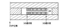
次に、コイルの導線幅を変化させた磁性素子(特開平11−40438号公報に開示)の、コイル中心軸から半径方向の断面図を図14および図15に示す。図13の例とはコイル24の形状が異なり、コイルの導線幅を、その部分を鎖交する磁束の強さに応じて変えることによって、高周波領域における抵抗損失の低減が図られている。また、この磁性素子では、渦電流による損失を同時に低減させることができる。コイルを鎖交する磁束によってコイルに渦電流が発生するため、鎖交する磁束の強い領域(コイル最内周付近および最外周付近)におけるコイル導線幅を相対的に狭くすることにより、渦電流の発生を低減できるからである。図14の例では、コイル最内周から数ターン、および最外周のコイルの導線幅が狭められている。図15の例では、コイル最内周から数ターンおよび最外周から数ターンのコイルの導線幅が狭められている。
【0006】
【発明が解決しようとする課題】
しかしながら、上記したような均等幅の導線からなるコイルを持つ磁性素子では、磁心から漏れた磁束の多くが、最内周付近のコイルを通るため、渦電流による損失が発生するという問題があった。特に小型、薄型を目指した磁性素子では、コイル導線の必要な幅の確保や、インダクタンス、直流抵抗、直流重畳特性などの特性維持のために、コイル中心部分に十分な断面積を確保することが難しい。そのため、中心部分を通れない磁束が、外側に漏れる程度がより強くなってしまう。また、コイル中心部分に置かれる磁性体に低透磁率の素材を用いた場合や、ギャップを設けた場合などにおいても、漏れ磁束の量は増大する。このような漏れ磁束を原因とした渦電流による損失は、小型化、薄型化に対応するためにコイルの導線幅が広がれば広がるほど大きくなる。また、渦電流による損失は、コイルに流れる電流が高周波になるほど大きくなる。そのため、小型、薄型を目指した磁性素子を、高周波スイッチングを行う電源などに用いる場合、とりわけ損失が増え、全体の効率が低下することになる。
【0007】
一方、特開平11−40438号公報に記載の磁性素子において、コイルを鎖交する磁束の強さのみを考慮してコイルの導線幅を変化させており、上記のような渦電流による損失の低減を図ることができる。しかし、この方法では周長の長い外周部分のコイルの導線幅をも狭くすることから、渦電流による損失を低減させることはできるが、全体の直流抵抗が増加してしまうという問題があった。特に、電源装置などの、主に直流電流を流す用途で用いる磁性素子の場合、この直流抵抗の増加が損失の大きな要因となり、低損失の磁性素子を得るといった目的を達成することが難しくなる。
【0008】
【課題を解決するための手段】
上記課題を解決するために本発明の磁性素子は、コイルを含む磁性素子であって、前記コイルの最外周の導線幅が、最内周の導線幅よりも広く、前記コイルの導線が、互いに並列接続している複数の分割導線を含み、前記並列接続している分割導線の数が、コイル外周の導線ほど多いことを特徴とする。
本発明の別の磁性素子は、コイルを含む磁性素子であって、前記コイルの最外周の導線幅が、最内周の導線幅よりも広く、前記コイルが、平角銅線を用いて構成されていることを特徴とする。
本発明のさらに別の磁性素子は、コイルを含む磁性素子であって、前記コイルの最外周の導線幅が、最内周の導線幅よりも広く、前記コイルが、ソレノイド状のコイルを用いて構成されていることを特徴とする。
本発明のさらに別の磁性素子は、コイルを含む磁性素子であって、前記コイルの導線が、互いに並列接続している複数の分割導線を含み、前記並列接続している分割導線の数が、コイル外周の導線ほど多いことを特徴とする。
【0009】
上記の磁性素子において、コイル最外周の導線幅が、コイルの導線の中で最大であることが好ましい。コイルの導線のうち、最外周の周長が最も長いため、最外周の導線幅を最大とすることでコイルの抵抗による損失をより効果的に低減させることができる。
【0010】
上記いずれかの磁性素子において、コイルの導線幅が、最内周から最外周にかけて次第に変化しているものであってもよいし、段階的に変化しているものであっても構わない。
【0011】
本発明の磁性素子は、コイルを含む磁性素子であって、上記コイルの導線が、互いに並列接続している複数の分割導線を含むことを特徴としている。また、最外周の導線幅が最内周の導線幅よりも広いことを特徴とするコイルの導線が、互いに並列接続している複数の分割導線を含むことが好ましい。ここで分割導線とは、コイルの導線を、スリットなどを設けることで複数に分割したそれぞれの部分のことであり、複数の分割導線が並列接続することで、コイルの導線を形成している。並列接続している分割導線同士は、コイルの同じ周を構成していることになる。例えば、図4あるいは図5における8がこの分割導線に相当し、並列接続することで導線7を形成している。このように、コイルの導線を分割することにより、渦電流による損失の低減と、抵抗による損失の低減とを同時に行うことができる。また、並列接続している分割導線に、ねじりを加えるなどで螺旋状にすることで、渦電流による損失の低減をさらに図ることができる。
【0012】
上記いずれかの磁性素子において、コイル最外周の導線が、互いに並列接続している複数の分割導線を含むことが好ましい。また、コイル最内周の導線が、互いに並列接続している複数の分割導線を含むことが好ましい。コイル最外周および最内周においてコイルを鎖交する磁束が強いため、このような構造を含むことで、渦電流による損失をより低減させることができる。また、コイルの抵抗を低減させる目的などで、コイル最外周の導線幅を大きくした場合に特に効果的となる。
【0013】
上記いずれかの磁性素子において、並列接続している分割導線の数が、コイル外周の導線ほど多いことが好ましい。
【0014】
上記いずれかの磁性素子において、並列接続している分割導線の幅が、互いに等しいことが好ましい。
【0015】
上記いずれかの磁性素子において、分割導線間の空隙の幅が、導線間の空隙の幅以下であることが好ましい。
【0016】
上記いずれかの磁性素子において、コイルが平板状であることが好ましい。平板状であれば、磁性素子を小型、薄型にすることができる。
【0017】
上記いずれかの磁性素子において、コイルが、少なくとも1層の、プリント基板上に形成されたコイルパターンを用いて構成されていることが好ましい。また、上記の磁性素子において、コイルパターンが、渦巻状のスリットを用いて得たコイルパターンであることが好ましい。
【0018】
上記いずれかの磁性素子において、コイルが、平角銅線を用いて構成されていることが好ましい。また、上記の磁性素子において、コイルが、平角銅線を、磁心となる磁性体の周りに巻回したものであることが好ましい。
【0019】
上記いずれかの磁性素子において、コイルが、ソレノイド状のコイルを用いて構成されていることが好ましい。
【0020】
上記いずれかの磁性素子において、複数のコイルを含み、上記コイルが互いに磁気的に結合していることが好ましい。
【0021】
上記いずれかの磁性素子において、コイルの面方向に、第1の磁性体を積層した構造であることが好ましい。また、第1の磁性体が、平板状であることが好ましい。上記いずれかの磁性素子において、コイルの中心および外周の少なくとも一方に、第2の磁性体を配置した構造を含むことが好ましい。なお、第1の磁性体と第2の磁性体は、同一の材料を用いたものであっても構わないし、必要に応じて一体化されていてもよい。
【0022】
本発明の電源は、上記いずれかの磁性素子を含むことを特徴としている。
【0023】
上記した磁性素子は、最内周付近のコイルで多く発生する渦電流による損失を低減しつつ、コイルの有する直流抵抗による損失も同時に低減可能とすることができる。その結果、小型、薄型、かつ低損失な磁性素子を提供することができる。また、これらの磁性素子を用いることで、小型で高効率の電源を提供することができる。
【0024】
【発明の実施の形態】
以下、本発明における実施の形態について図面を参照しながら説明する。
【0025】
(実施の形態1)
本発明における実施の形態1について図1〜図3を用いて説明する。
【0026】
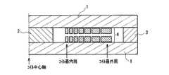
図1〜図3は、本実施の形態における磁性素子の例を示す、コイル中心軸から半径方向の断面図である。コイル4の両面に平板状の磁性体1が積層され、コイル最内周内側の中心部にあたる磁心2、およびコイル最外周外側の外周部にあたる外足3には磁性体が配置されている。コイル4は互いに接続された上下2層から成り立っており、合計14ターンとなっている。図13〜図15に示す従来例とは、コイル4以外は同じ構成となっている。
【0027】
図1〜図3に示すように、コイル4は、従来例とは異なり、内周から外周に進むにつれて各周におけるコイルの導線幅が次第に広くなり、最内周の導線幅よりも最外周の導線幅が広くなった構造を特徴としている。
【0028】
言い換えれば、各周におけるコイルの導線幅を、最内周から順に、W1、W2、…、Wn−1、Wn、…、Wp(n:2〜pの整数、Wn>0、Wp:コイル最外周の導線幅)とするとき、Wn−1≦Wn、かつW1<Wpという関係が成り立てばよいことを意味している。また、このとき、部分的にWn−1≦Wnの不等号の向きが逆転していても、その差がもたらす直流抵抗値の増加分がわずかであって、全体として内周の導線幅が狭く外周の導線幅が広い傾向をもつコイルであれば構わない。
【0029】
また、なかでも、コイル最外周の導線幅Wpが、コイルの他の周の導線幅と比較して最大であることが好ましい。コイルの導線のうち、最外周の周長が最も長いためである。
【0030】
本実施の形態における磁性素子は、コイル4が、このような特徴を持つものであればよい。このような特徴を持つコイルであれば、図14および図15に示したような従来例とは異なり、渦電流による損失の低減と、直流抵抗による損失の低減とを同時に図ることができる。
【0031】
例えば、上記の構造を実現するために、図1の例では、各周におけるコイルの導線が、中心軸からの半径に比例した幅を持つように設計されている。これは、図2に示すように半径の2乗に比例した導線幅を持つコイルであってもよいし、図3に示すように3段階に分けられた導線幅を持つコイルであっても構わない。このようにコイルの導線幅は、最内周から最外周方向に対して、段階的に増加していても一律に増加していても構わない。
【0032】
コイルとしては、特に限定されないが、平板状に形成されたものであることが、小型、薄型化のために好ましい。平板状に形成されたコイルとしては、例えば、プリント基板上にあるコイルパターンなどを用いることができる。このようなコイルパターンは、渦巻状のスリットを用いて得ることができる。
【0033】
その他、コイルとして、通常の平角銅線や丸銅線をコイル状にしたものを用いることも可能であり、エッチングやメッキ成長などの、コイルの導線幅を任意に制御できるプロセスによって得たコイルを用いることもできる。
【0034】
なお、コイル4のターン数は、図1〜図3に示す14に限定されるものではない。必要な磁気特性に応じて任意に設定することができる。
【0035】
また、図1〜図3ではコイル4は上下2層の構造になっているが、単層であっても、それぞれのコイル層が接続されていれば3層以上の複数層であっても構わない。層の数は必要な磁気特性に応じて任意に設定することができる。また、接続の方法は直列であっても並列であっても構わない。
【0036】
コイル4のみでも磁性素子として成立するが、図1〜図3に示すようにコイル4の両面に磁性体1を積層することが好ましく、また、磁心2および外足3の部分にも磁性体が配置されることが好ましい。磁性体1は、所望の磁路を確保できるものであれば、形状は限定されないが、小型、薄型の磁性素子のためには、図1〜図3に示すような平板状が好ましい。
【0037】
磁性体1としては、特に限定されないが、なかでもフェライトを用いることが好ましい。また、磁心2および外足3に配置される磁性体としては、特に限定されないが、圧粉磁心材のようなコンポジット磁性材料を用いることが好ましい。第1の磁性体と第2の磁性体は、同一の材料を用いたものであっても構わないし、必要に応じて一体化されていてもよい。
【0038】
本実施の形態における図1〜図3に示す磁性素子と、従来例である図13〜図15に示す磁性素子との特性比較の結果を下記の表1に示す。特性として、インダクタンスと、渦電流による損失を反映するパラメーターである交流抵抗と、直流抵抗とを、有限要素法を用いて算出した。交流抵抗は、1MHz時のものを用いた。図1〜図3にあたるものが、実施例1〜実施例3であり、図13〜図15にあたるものが、比較例1〜比較例3である。また、実施例4として、図1にあたるコイルの、最内周と最外周の間で一部導線幅の変化を逆転させたもの(最内周から数えて3周目と4周目のコイル幅を逆転:上記のWn−1≧Wnの状態にあたる)を用いた。
【0039】
有限要素法に基づく特性解析は、下記の表2および表3に示すパラメーターにて行った。表2に、実施例および比較例として用いたコイルの各周の導線幅を示す。表2における「2T」、「3T」などはそれぞれコイルの最内周から数えて2ターン目(2周目)、3ターン目(3周目)であることを意味している。表2に示す各コイルのターン数は7であるが、これを直列接続で2層積層させ、それぞれターン数が14のモデルとした。また、表3に示すように、実施例および比較例に用いるコイルとして、同一の最内径、最外径、厚み、材質のものを想定し、磁性体もすべて同じ材質のものを想定した。なお、表3の磁性体材料を示す欄において、「A部」とは、図1〜図3に示す磁性体1および図13〜図15に示す磁性体21に相当する部分のことであり、「B部」とは、図1〜図3に示す磁心2、外足3、および、図13〜図15に示す磁心22、外足23に相当する部分のことである。
【0040】
また、各実施例および比較例において、図1〜図3および図13〜図15に示すそれぞれの断面図を中心軸に対して一回転させたモデルを用いた。
【0041】
【表2】
【表3】
表1の結果によれば、実施例および比較例ともに、インダクタンスはすべてほぼ同一であると言える。しかし内周に比べて周長の長い外周部分の導線幅が相対的に広がっている実施例1では、全周にわたって等幅の導線を用いている比較例1に比べ、渦電流による損失低減と直流抵抗による損失低減とが同時に実現できていることがわかる。実施例2および実施例3では、実施例1に比べるとわずかに直流抵抗が上昇しているものの、特に交流抵抗が大きく減少していることがわかる。また、交流抵抗を減らすためにコイルの外周の導線幅を狭くした構造である比較例2および比較例3と比べても、交流抵抗がさらに大きく減少しており、かつ直流抵抗の低減効果も十分大きいと言える。
【0045】
また、一部コイルの導線幅の変化が逆転した構造である実施例4においても、比較例に対して、交流抵抗および直流抵抗の双方の低減が実現できていることがわかる。
【0046】
上記の実施例および比較例では、コイル両面に平板状の磁性体を積層し、磁心および外足にも磁性体が存在する場合を示したが、その他、コイルを鎖交する磁束がより大きい場合においても、渦電流による損失の低減と直流抵抗による損失の低減という両方の効果を得ることができ、相乗的な損失の低減を図ることができる。鎖交磁束が大きい場合としては、コイルのみが存在する場合、コイル両面に磁性体を積層してあるが、磁心が空芯である場合、磁心または外足に透磁率の高い磁性体を用いているが、ギャップが存在する場合、その他、ギャップはないものの、コイル両面の磁性体よりも透磁率の低い材料で磁心または外足を構成してある場合などが考えられる。
【0047】
なお、上記の実施例および比較例では、全体の形が円盤状のモデルを考えて比較したが、その他、円形、楕円形および四角形など、コイルを形成する上で可能な形であれば、どのようなものであっても同様の効果を得ることができる。
【0048】
さらに、中心から見て全方向の導線が上記した特徴を持つコイルであることが最も好ましいが、磁性素子の形状などにより上記した特徴が部分的に満たされない場合でも本発明の効果を得ることができる。
【0049】
(実施の形態2)
以下、本発明における実施の形態2について、図面を参照しながら説明する。
【0050】
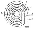
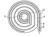
図4〜図6は、本実施の形態における磁性素子の例を示す模式図である。図4〜図6に示すように、本実施の形態の磁性素子は、磁心2を中心に渦巻状のコイル4が配置されており、コイル4の導線7が、並列接続している複数の分割導線8に分けられた分割構造を含んでいることを特徴としている。
【0051】
ここで分割導線とは、コイルの導線を、スリットなどを設けることで複数に分割したそれぞれの部分のことである。図4〜図6に示すように、複数の分割導線8が並列接続することで、導線7を形成しており、並列接続している分割導線8同士は、コイルの同じ周を構成していることになる。このような分割構造にするためには、導線にスリットなどを設ければよい。また、逆に独立した複数の導線を、分割導線として並列接続させ、その集合体をひとつの大きな導線として機能させても構わない。さらに、並列接続している分割導線に、ねじりを加えるなどで螺旋状にすることで、渦電流による損失の低減をより図ることができる。
【0052】
なお、このように分割構造を設けた部分のコイルの導線幅は、磁束と直交する分割導線の幅の和とすることができる。
【0053】
上記したような分割構造を含むコイルを用いることで、直流抵抗による損失を増加させることなく、渦電流による損失を同時に低減させた磁性素子を得ることができる。
【0054】
例えば、図6に示すように、導線幅が等幅であるコイルの最外周および最内周に対して本発明の分割構造を与えた場合、図13に示す従来例の等幅導線コイルに比べて渦電流による損失を効果的に低減させることができる。
【0055】
また図6の例では、図14および図15に示す従来例のように、鎖交磁束の強度に応じてコイルの導線幅を減少させるのではなく、分割構造を設けることにより渦電流による損失を低減させている。そのため、コイルの最内周、最外周の導線幅を等価的に最低必要なだけ確保することができ、従来例で見られた、導線幅の減少によって直流抵抗値が大きくなるデメリットを克服することが可能となる。
【0056】
この場合、分割構造は、コイルを鎖交する磁束がコイル最外周および最内周において特に強いため、コイルの最内周または最外周に、あるいは必要に応じて最内周および最外周に同時に設ければよい。また、それぞれの周の一周すべてにわたって分割構造を設けることが好ましいが、少なくとも周の一部に分割構造を設ければ、本発明の効果を得ることができる。
【0057】
また必要に応じて、コイルの最外周から2周まで、最内周から2周までの導線に対して分割構造を設けることもできる。
【0058】
さらにこのような分割構造は、実施の形態1で示したコイルと同様の、外周ほど導線幅が広くなったコイルに対して導入することもできる。その例を図4および図5に示す。図4および図5に示す例では、外周ほど導線幅が広くなったコイル4に分割構造が設けられている。コイルをこのような構成にすることで、渦電流および直流抵抗による両損失を、より効果的に低減させることができる。
【0059】
分割構造は、全周にわたって設けても、一部分に設けても、どちらでも構わない。なかでもコイルを鎖交する磁束の大きい最内周や、コイルの導線幅が相対的に広くなっているコイル4の外周部分に分割構造を設けることがより効果的である。また特に、最外周に設けることが好ましい。最外周が最も周長が長く、抵抗による損失を低減させるために導線幅を広くとる必要があることと、コイルを鎖交する磁束が大きいため、分割構造を導入する効果が大きいからである。また、外周になるにつれてコイルの導線幅が広くなるため、図5に示すように外周ほど分割導線8の数が多いことが好ましい。
【0060】
また、その他、上記した以外の導線幅の傾向を持つコイルに対しても、同様の効果を得ることができる。
【0061】
本実施の形態において、分割導線8の幅は、それぞれ互いに等しいことが好ましい。互いに等しい場合に、最も本発明の効果を得ることができる。
【0062】
また、分割導線8が部分的に導通していても何ら問題はないため、分割導線間の空隙5の幅を、導線間の空隙6の幅以下にすることが好ましい。このような構造を用いた場合、コイルの断面積の減少を最小限に押さえることができ、分割構造の存在による直流抵抗の増加を低減させることができる。
【0063】
図4〜図6にはコイル4の磁心にのみ磁性体が示されているが、実施の形態1におけるコイルと同様に、コイル外周部や、コイルの面方向に磁性体を設ければ特性をより向上させることができる。その他、コイルを鎖交する磁束がより大きい場合においても、渦電流による損失の低減と直流抵抗による損失の低減という両方の効果を得ることができ、相乗的な損失の低減を図ることができる。なお実施の形態1と同様に、本発明の効果はコイルの形状に左右されないため、コイルを形成する上で可能な形であれば、どのような形状であっても構わない。
【0064】
(実施の形態3)
以下、本発明における実施の形態3について、図面を参照しながら説明する。
【0065】
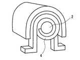
図7は、本実施の形態におけるチョークコイルの例を示す断面図である。図7に示すように、チョークコイルは、磁心2の周囲にコイル4を巻回した構造を含む磁性素子の1種である。
【0066】
このときコイル4が、実施の形態1および2と同様のコイルであれば、渦電流による損失と直流抵抗による損失との双方が低減された、低損失のチョークコイルとすることができる。チョークコイルの場合、なかでも直流抵抗による損失の低減が重要であり、本発明におけるコイル4を用いる効果がとりわけ大きくなる。
【0067】
なぜなら、チョークコイルは一般に、電気回路中の整流、平滑部分に用いられるため、流れる電流は直流重畳された電流であり、負荷が極端に軽い場合を除けば、直流成分の占める割合が高くなる。そのためコイルに流れる電流の実効値を考えた場合、交流成分の割合は少なく、直流成分が大半を占めており、コイルで発生する損失も直流抵抗損失が支配的になるからである。
【0068】
このように損失を低減したコイルは、素子の発熱も抑制できるため、一般的に高価とされている耐熱性の高い絶縁材料や、高効率な放熱手段を用いる必要がないため、小型、薄型の機器を安価に提供することが可能となる。
【0069】
また、本実施の形態における磁性素子において、コイルが平角銅線を用いて構成されていることが好ましい。平角銅線を用いた場合、コイル導線の断面積が大きいため、平板状のコイルでは流せないような大電流に対応させることができるからである。平角銅線により構成されたコイルを有するチョークコイルの例を、図8に示す。磁心2のまわりに平角銅線を用いて構成されたコイル4が巻回された構造をしている。
【0070】
図8に示す構造は、例えば、図9に示すような方法を用いて得ることができる。図9に示すように、幅を徐々に、あるいは段階的に変化させた平角銅線9を磁心2の周囲に巻回すればよい。このとき、磁心2にもっとも近い部分の銅線の幅が狭く、磁心2から離れるにつれて幅を太くした平角銅線9を用いれば、本実施の形態における磁性素子を得ることができる。
【0071】
なお、巻回する際には平角銅線9と磁心2とを絶縁させるために、両者の間に絶縁物を配置しても構わない。絶縁物としては例えば、磁心2となる磁性体の周囲をカバーするボビンなどを用いることができる。絶縁物の材料としては、樹脂など、絶縁物として一般的に用いられているものを用いることができる。
【0072】
また、本実施の形態において、磁性素子の損失が大きく低減されているため、磁心となる磁性体には、金属圧粉材料などの透磁率の低い材料から、フェライトなどの透磁率の高い材料まで、様々な磁性材料を用いることができる。また、磁心がギャップを有していても構わない。
【0073】
(実施の形態4)
以下、本発明における実施の形態4について、図面を参照しながら説明する。
【0074】
図10は、本実施の形態におけるトランスの例を示す断面図である。図10に示すように、トランスは、複数のコイル4が磁気的に結合している構造を含む磁性素子の1種である。
【0075】
スイッチング電源などの電子機器にこのようなトランスを用いた場合、コイル4には整流素子やスイッチ素子などが接続されることになり、直流重畳された電流成分が多く流れることになる。
【0076】
このとき、実施の形態1および2と同様なコイルが少なくとも1つ含まれていれば、実施の形態1〜3と同様に、低損失な磁性素子を実現することができる。
【0077】
(実施の形態5)
以下、本発明における実施の形態5について、図面を参照しながら説明する。
【0078】
図11は、本実施の形態における磁性素子の例を示す断面図である。図11に示す磁性素子において、コイル4としてソレノイド型コイルを用いたことが大きな特徴となっている。
【0079】
このようにソレノイド型のコイルを用いた場合であっても、磁心2からの漏れ磁束は、コイル中心軸に平行する成分が主体であるため、鎖交磁束の強度はコイル中心軸から半径方向の距離によって決まるといえる。したがってコイル4を、実施の形態1〜4と同様の形態を持ったソレノイド型コイルにすることにより、渦電流による損失と直流抵抗による損失とを同時に効果的に低減することができる。その結果、小型、薄型かつ低損失な磁性素子を実現することができる。
【0080】
(実施の形態6)
以下、本発明における実施の形態6について、図面を参照しながら説明する。
【0081】
図12は、本発明における磁性素子を用いて構成された電源の例を示す断面図である。
【0082】
図12に示すように、本発明における磁性素子10を、直流出力の平滑チョークとして、またはトランスなどとして用いれば、渦電流による損失と直流抵抗による損失とを同時に、効果的に低減することができる。その結果、小型、薄型かつ低損失な電源を実現することができる。
【0083】
さらに、この磁性素子を、コンデンサ12、電源制御IC11、スイッチング素子、整流素子などと一体化して立体的に配置することで電源そのものをより小型化することができる。このような電源は、高さ、大きさ、底面積、発熱などの制約の多い負荷の近傍に配置することが可能であり、耐ノイズ性能の向上やパターンの配線が短くなることによる損失低減効果、コンデンサ電極を利用したシールド効果などの相乗効果も期待することができる。
【0084】
【発明の効果】
以上説明したように、本発明によれば、渦電流による損失の低減と、直流抵抗による損失の低減とを同時に達成することのできる、低損失な磁性素子を提供することができる。また、その磁性素子を用いることで、低損失の電源を提供することができる。
【図面の簡単な説明】
【図1】本発明における磁性素子の例を示す断面図
【図2】本発明における磁性素子の例を示す断面図
【図3】本発明における磁性素子の例を示す断面図
【図4】本発明における磁性素子に用いられるコイルの例を示す模式図
【図5】本発明における磁性素子に用いられるコイルの例を示す模式図
【図6】本発明における磁性素子に用いられるコイルの例を示す模式図
【図7】本発明における磁性素子の例を示す断面図
【図8】本発明における磁性素子の例を示す模式図
【図9】本発明における磁性素子の製造方法例を示す模式図
【図10】本発明における磁性素子の例を示す断面図
【図11】本発明における磁性素子の例を示す断面図
【図12】本発明における電源の例を示す断面図
【図13】従来における磁性素子の例を示す断面図
【図14】従来における磁性素子の例を示す断面図
【図15】従来における磁性素子の例を示す断面図
【符号の説明】
1、21 磁性体
2、22 磁心
3、23 外足
4、24 コイル
5 分割導線間の空隙
6 導線間の空隙
7 導線
8 分割導線
9 平角銅線
10 磁性素子
11 電源制御IC
12 コンデンサ[0001]
BACKGROUND OF THE INVENTION
The present invention relates to a small, thin, and low loss magnetic element used for a switching power supply device that supplies DC stabilized power to industrial and consumer electronic devices, and a power source using the magnetic element. It is.
[0002]
[Prior art]
In recent years, with the downsizing, thinning, high performance, and energy saving of electronic devices, magnetic elements used for these devices are strongly demanded to be smaller, thinner, and have lower loss. There are mainly two types of loss that occur in the magnetic element: iron loss and copper loss. Copper loss is a loss mainly caused by the DC resistance component of the coil included in the magnetic element, and iron loss is a loss mainly caused by the eddy current generated in the magnetic body and coil contained in the magnetic element. is there. Therefore, in order to reduce the loss of the magnetic element, it is necessary to consider both the loss due to the resistance of these coils and the loss due to the eddy current.
[0003]
Hereinafter, a configuration example of a conventional magnetic element will be described.
[0004]
First, FIG. 13 shows a cross-sectional view in the radial direction from the coil central axis of a magnetic element having a coil made of a conductor having a uniform width. In the example of FIG. 13, a flat plate-like
[0005]
Next, FIGS. 14 and 15 are sectional views of a magnetic element (disclosed in Japanese Patent Laid-Open No. 11-40438) in which the coil conductor width is changed in the radial direction from the coil central axis. The shape of the
[0006]
[Problems to be solved by the invention]
However, in the magnetic element having a coil made of a conductor having a uniform width as described above, there is a problem that loss due to eddy current occurs because most of the magnetic flux leaking from the magnetic core passes through the coil near the innermost circumference. . In particular, in a magnetic element aimed at small size and thinness, it is necessary to secure a sufficient cross-sectional area in the central part of the coil in order to secure the necessary width of the coil conductor and to maintain the characteristics such as inductance, DC resistance, and DC superposition characteristics. difficult. Therefore, the degree to which the magnetic flux that cannot pass through the central portion leaks to the outside becomes stronger. The amount of leakage magnetic flux also increases when a low magnetic permeability material is used for the magnetic material placed in the center of the coil or when a gap is provided. The loss due to the eddy current caused by such leakage magnetic flux increases as the coil conductor width increases in order to cope with the reduction in size and thickness. Further, the loss due to the eddy current increases as the current flowing through the coil becomes higher in frequency. For this reason, when a magnetic element aiming at a small size and a thin thickness is used for a power source that performs high-frequency switching, the loss is particularly increased and the overall efficiency is lowered.
[0007]
On the other hand, in the magnetic element described in Japanese Patent Application Laid-Open No. 11-40438, the conductor wire width of the coil is changed considering only the strength of the magnetic flux interlinking the coil, and the loss due to the eddy current as described above is reduced. Can be achieved. However, this method narrows the conductive wire width of the coil in the outer peripheral portion having a long peripheral length, so that the loss due to the eddy current can be reduced, but there is a problem that the overall DC resistance increases. In particular, in the case of a magnetic element used mainly for applications where a direct current flows, such as a power supply device, this increase in direct current resistance becomes a major cause of loss, making it difficult to achieve the purpose of obtaining a low loss magnetic element.
[0008]
[Means for Solving the Problems]
In order to solve the above problems, the magnetic element of the present invention is a magnetic element including a coil, and the outermost conductor wire width of the coil is wider than the innermost conductor wire width.In addition, the conducting wire of the coil includes a plurality of divided conducting wires connected in parallel to each other, and the number of the divided conducting wires connected in parallel is larger as the conducting wire on the outer periphery of the coil.With featuresDo.
Another magnetic element of the present invention is a magnetic element including a coil, wherein the outermost conductor wire width of the coil is wider than the innermost conductor wire width, and the coil is configured using a flat copper wire. It is characterized by.
Yet another magnetic element of the present invention is a magnetic element including a coil, wherein the outermost conductor wire width of the coil is wider than the innermost conductor wire, and the coil is a solenoid coil. It is configured.
Still another magnetic element of the present invention is a magnetic element including a coil, wherein the conductive wire of the coil includes a plurality of divided conductive wires connected in parallel to each other, and the number of the divided conductive wires connected in parallel is It is characterized in that there are more conductors on the outer periphery of the coil.
[0009]
In the above magnetic element, it is preferable that the outermost conductor wire width of the coil is the largest among the coil conductor wires. Since the circumference of the outermost periphery is the longest among the conductors of the coil, the loss due to the resistance of the coil can be more effectively reduced by maximizing the width of the outermost conductor.
[0010]
In any one of the above magnetic elements, the coil wire width may be gradually changed from the innermost periphery to the outermost periphery, or may be changed stepwise.
[0011]
The magnetic element of the present invention is a magnetic element including a coil, wherein the conductive wire of the coil includes a plurality of divided conductive wires connected in parallel to each other. Moreover, it is preferable that the conducting wire of the coil characterized in that the outermost conducting wire width is wider than the innermost conducting wire width includes a plurality of divided conducting wires connected in parallel to each other. Here, the divided conducting wire is a portion obtained by dividing the coil conducting wire into a plurality of portions by providing slits or the like, and the plurality of divided conducting wires are connected in parallel to form a coil conducting wire. The divided conducting wires connected in parallel constitute the same circumference of the coil. For example, 8 in FIG. 4 or FIG. 5 corresponds to this divided conductor, and the
[0012]
In any one of the magnetic elements described above, it is preferable that the outermost conductor of the coil includes a plurality of divided conductors connected in parallel to each other. Moreover, it is preferable that the conducting wire in the innermost circumference of the coil includes a plurality of divided conducting wires connected in parallel to each other. Since the magnetic flux interlinking the coils is strong in the outermost and innermost coils, the loss due to the eddy current can be further reduced by including such a structure. Further, it is particularly effective when the conductor wire width on the outermost periphery of the coil is increased for the purpose of reducing the resistance of the coil.
[0013]
In any one of the above magnetic elements, it is preferable that the number of the divided conducting wires connected in parallel is larger as the conducting wire on the outer periphery of the coil.
[0014]
In any one of the above magnetic elements, it is preferable that the widths of the divided conducting wires connected in parallel are equal to each other.
[0015]
In any one of the above magnetic elements, the width of the gap between the divided conductors is preferably equal to or less than the width of the gap between the conductors.
[0016]
In any one of the above magnetic elements, the coil is preferably flat. If it is flat, the magnetic element can be made small and thin.
[0017]
In any one of the above magnetic elements, the coil is preferably configured using a coil pattern formed on at least one layer of a printed board. In the above magnetic element, the coil pattern is preferably a coil pattern obtained using a spiral slit.
[0018]
In any one of the above magnetic elements, the coil is preferably configured using a flat copper wire. In the above magnetic element, the coil is preferably formed by winding a rectangular copper wire around a magnetic body serving as a magnetic core.
[0019]
In any one of the above magnetic elements, the coil is preferably configured using a solenoidal coil.
[0020]
Any one of the above magnetic elements preferably includes a plurality of coils, and the coils are magnetically coupled to each other.
[0021]
Any one of the above magnetic elements preferably has a structure in which the first magnetic body is laminated in the surface direction of the coil. Moreover, it is preferable that a 1st magnetic body is flat form. Any one of the above magnetic elements preferably includes a structure in which the second magnetic body is disposed at least one of the center and the outer periphery of the coil. In addition, the 1st magnetic body and the 2nd magnetic body may use the same material, and may be integrated as needed.
[0022]
The power supply according to the present invention includes any one of the above magnetic elements.
[0023]
The magnetic element described above can reduce the loss due to the DC resistance of the coil at the same time while reducing the loss due to the eddy current frequently generated in the coil near the innermost periphery. As a result, a small, thin, and low loss magnetic element can be provided. Further, by using these magnetic elements, a small and highly efficient power source can be provided.
[0024]
DETAILED DESCRIPTION OF THE INVENTION
Hereinafter, embodiments of the present invention will be described with reference to the drawings.
[0025]
(Embodiment 1)
A first embodiment of the present invention will be described with reference to FIGS.
[0026]
1 to 3 are cross-sectional views in the radial direction from the coil central axis, showing examples of magnetic elements in the present embodiment. Flat
[0027]
As shown in FIGS. 1 to 3, the
[0028]
In other words, the coil wire width in each circumference is set to W in order from the innermost circumference.1, W2... Wn-1, Wn... Wp(N: integer from 2 to p, Wn> 0, Wp: W of the outermost coil circumference)n-1≦ WnAnd W1<WpThis means that the relationship At this time, W is partiallyn-1≦ WnEven if the direction of the inequality sign is reversed, the difference in DC resistance caused by the difference is slight, and the coil having a tendency that the inner conductor wire width is narrow and the outer conductor wire width tends to be wide as a whole. Absent.
[0029]
In particular, the outermost conductor width W of the coilpHowever, it is preferable that it is the maximum compared with the conducting wire width of the other circumference | surroundings of a coil. This is because the outermost circumference has the longest circumference among the coil wires.
[0030]
The magnetic element in this Embodiment should just be the thing in which the
[0031]
For example, in order to realize the above-described structure, in the example of FIG. 1, the coil conductor wire in each circumference is designed to have a width proportional to the radius from the central axis. This may be a coil having a conductor width proportional to the square of the radius as shown in FIG. 2, or a coil having a conductor width divided into three stages as shown in FIG. Absent. As described above, the conductive wire width of the coil may be increased stepwise or uniformly from the innermost circumference to the outermost circumference direction.
[0032]
Although it does not specifically limit as a coil, It is preferable for a small size and thickness reduction to be formed in flat form. As the coil formed in a flat plate shape, for example, a coil pattern on a printed board can be used. Such a coil pattern can be obtained using a spiral slit.
[0033]
In addition, it is also possible to use a coil made of a normal rectangular copper wire or a round copper wire as a coil. A coil obtained by a process capable of arbitrarily controlling the coil conductor width, such as etching or plating growth, is used. It can also be used.
[0034]
The number of turns of the
[0035]
1 to 3, the
[0036]
Although only the
[0037]
Although it does not specifically limit as the
[0038]
Table 1 below shows the results of a characteristic comparison between the magnetic element shown in FIGS. 1 to 3 and the conventional magnetic element shown in FIGS. 13 to 15 in the present embodiment. As characteristics, AC resistance and DC resistance, which are parameters reflecting inductance, loss due to eddy current, were calculated using a finite element method. The AC resistance was 1 MHz. Examples corresponding to FIGS. 1 to 3 are Examples 1 to 3, and those corresponding to FIGS. 13 to 15 are Comparative Examples 1 to 3. Further, as Example 4, the coil corresponding to FIG. 1 is partially reversed in change of the conductor width between the innermost circumference and the outermost circumference (the coil widths in the third and fourth rounds counted from the innermost circumference). Reverse: W aboven-1≧ WnWhich corresponds to the state of
[0039]
The characteristic analysis based on the finite element method was performed using the parameters shown in Table 2 and Table 3 below. Table 2 shows the wire width of each circumference of the coil used as an example and a comparative example. “2T”, “3T”, etc. in Table 2 mean the second turn (second turn) and the third turn (third turn) from the innermost circumference of the coil. Although the number of turns of each coil shown in Table 2 is 7, two layers are stacked in series connection to form a model with 14 turns. As shown in Table 3, the coils used in the examples and comparative examples were assumed to have the same innermost diameter, outermost diameter, thickness, and material, and all the magnetic materials were assumed to be the same material. In the column showing the magnetic material in Table 3, “A part” is a part corresponding to the
[0040]
In each example and comparative example, models were used in which the respective cross-sectional views shown in FIGS. 1 to 3 and FIGS. 13 to 15 were rotated once with respect to the central axis.
[0041]
[Table 2]
[Table 3]
According to the results in Table 1, it can be said that all the inductances are substantially the same in both the example and the comparative example. However, in Example 1 in which the conductor width of the outer peripheral portion having a longer circumference than the inner periphery is relatively wide, loss due to eddy current is reduced compared to Comparative Example 1 in which a conductor having a uniform width is used over the entire circumference. It can be seen that loss reduction due to DC resistance can be realized at the same time. In Example 2 and Example 3, although the direct current resistance slightly increased compared to Example 1, it can be seen that the alternating current resistance is greatly reduced. In addition, compared with Comparative Example 2 and Comparative Example 3 in which the conductor width on the outer periphery of the coil is narrowed in order to reduce the AC resistance, the AC resistance is further greatly reduced, and the effect of reducing the DC resistance is sufficient. It can be said that it is big.
[0045]
It can also be seen that in Example 4 which is a structure in which the change in the conductor width of some coils is reversed, both the AC resistance and the DC resistance can be reduced as compared with the comparative example.
[0046]
In the above-mentioned examples and comparative examples, the case where the flat magnetic material is laminated on both sides of the coil and the magnetic material is also present on the magnetic core and the outer leg is shown. However, when the magnetic flux interlinking the coil is larger In this case, it is possible to obtain both the effects of reduction of loss due to eddy current and reduction of loss due to DC resistance, and synergistic reduction of loss can be achieved. When the flux linkage is large, when only the coil is present, magnetic bodies are laminated on both sides of the coil, but when the magnetic core is an air core, use a magnetic material with high permeability for the magnetic core or outer leg. However, when there is a gap, there may be a case where a magnetic core or an outer leg is made of a material having a lower magnetic permeability than the magnetic bodies on both sides of the coil, although there is no gap.
[0047]
In the above-mentioned examples and comparative examples, the overall shape was compared in consideration of a disk-shaped model. However, any shape that can be used to form a coil, such as a circle, an ellipse, and a rectangle, can be used. Even if it is such, the same effect can be acquired.
[0048]
In addition, it is most preferable that the conductive wire in all directions when viewed from the center is a coil having the above-described characteristics, but the effect of the present invention can be obtained even when the above-described characteristics are not partially satisfied due to the shape of the magnetic element or the like. it can.
[0049]
(Embodiment 2)
The second embodiment of the present invention will be described below with reference to the drawings.
[0050]
4 to 6 are schematic views showing examples of the magnetic element in the present embodiment. As shown in FIGS. 4 to 6, in the magnetic element of the present embodiment, a
[0051]
Here, the divided conducting wire is a portion obtained by dividing the conducting wire of the coil into a plurality of parts by providing a slit or the like. As shown in FIGS. 4 to 6, a plurality of divided conducting
[0052]
In addition, the conducting wire width of the portion of the coil provided with the dividing structure in this way can be the sum of the widths of the dividing conducting wires orthogonal to the magnetic flux.
[0053]
By using the coil including the divided structure as described above, it is possible to obtain a magnetic element in which loss due to eddy current is simultaneously reduced without increasing loss due to DC resistance.
[0054]
For example, as shown in FIG. 6, when the divided structure of the present invention is applied to the outermost and innermost coils of the coil having the same width, the comparison with the conventional equal-width coil shown in FIG. Thus, loss due to eddy current can be effectively reduced.
[0055]
Moreover, in the example of FIG. 6, unlike the conventional example shown in FIG. 14 and FIG. It is reduced. Therefore, the innermost and outermost conductor wire widths of the coil can be assured equivalently as much as necessary, and the disadvantage of increasing the DC resistance due to the reduction of the conductor wire width seen in the conventional example is overcome. Is possible.
[0056]
In this case, since the magnetic flux interlinking the coils is particularly strong in the outermost and innermost circumferences of the coil, the split structure is provided at the innermost or outermost circumference of the coil, or at the same time on the innermost and outermost circumferences as necessary. Just do it. Moreover, although it is preferable to provide a divided structure over the entire circumference of each circumference, the effect of the present invention can be obtained if the divided structure is provided at least at a part of the circumference.
[0057]
Further, if necessary, a split structure can be provided for the conducting wire from the outermost circumference to the second circumference and from the innermost circumference to the second circumference.
[0058]
Further, such a divided structure can also be introduced into a coil having a conductor wire width wider toward the outer periphery, similar to the coil shown in the first embodiment. Examples thereof are shown in FIGS. In the example shown in FIG. 4 and FIG. 5, the split structure is provided in the
[0059]
The divided structure may be provided over the entire circumference or may be provided in a part. In particular, it is more effective to provide a split structure at the innermost circumference where the magnetic flux interlinking the coils is large or at the outer circumference of the
[0060]
In addition, the same effect can be obtained for a coil having a tendency of a wire width other than those described above.
[0061]
In the present embodiment, it is preferable that the widths of the divided conducting
[0062]
In addition, since there is no problem even if the divided conducting
[0063]
4 to 6 show the magnetic material only in the magnetic core of the
[0064]
(Embodiment 3)
[0065]
FIG. 7 is a cross-sectional view showing an example of the choke coil in the present embodiment. As shown in FIG. 7, the choke coil is one type of magnetic element including a structure in which a
[0066]
At this time, if the
[0067]
This is because the choke coil is generally used for a rectifying and smoothing portion in an electric circuit, and thus the flowing current is a DC superimposed current, and the ratio of the DC component is high except when the load is extremely light. For this reason, when considering the effective value of the current flowing through the coil, the ratio of the AC component is small, the DC component is the majority, and the DC resistance loss is dominant in the loss generated in the coil.
[0068]
Since the coil with reduced loss can suppress the heat generation of the element, it is not necessary to use a heat-resistant insulating material that is generally expensive and a highly efficient heat dissipation means. Equipment can be provided at low cost.
[0069]
In the magnetic element according to the present embodiment, it is preferable that the coil is configured using a flat copper wire. This is because when a rectangular copper wire is used, the coil conductor has a large cross-sectional area, so that a large current that cannot be flowed by a flat coil can be handled. An example of a choke coil having a coil made of a flat copper wire is shown in FIG. A
[0070]
The structure shown in FIG. 8 can be obtained using, for example, a method as shown in FIG. As shown in FIG. 9, a
[0071]
In order to insulate the
[0072]
In the present embodiment, since the loss of the magnetic element is greatly reduced, the magnetic material to be the magnetic core ranges from a material having a low magnetic permeability such as a metal dust material to a material having a high magnetic permeability such as ferrite. Various magnetic materials can be used. The magnetic core may have a gap.
[0073]
(Embodiment 4)
[0074]
FIG. 10 is a cross-sectional view showing an example of a transformer in the present embodiment. As shown in FIG. 10, the transformer is one type of magnetic element including a structure in which a plurality of
[0075]
When such a transformer is used for an electronic device such as a switching power supply, a rectifier element, a switch element, or the like is connected to the
[0076]
At this time, if at least one coil similar to that in the first and second embodiments is included, a low-loss magnetic element can be realized as in the first to third embodiments.
[0077]
(Embodiment 5)
The fifth embodiment of the present invention will be described below with reference to the drawings.
[0078]
FIG. 11 is a cross-sectional view showing an example of the magnetic element in the present embodiment. The magnetic element shown in FIG. 11 is characterized in that a solenoid type coil is used as the
[0079]
Even when a solenoid type coil is used in this way, the leakage magnetic flux from the
[0080]
(Embodiment 6)
[0081]
FIG. 12 is a cross-sectional view showing an example of a power source configured using the magnetic element of the present invention.
[0082]
As shown in FIG. 12, if the
[0083]
Furthermore, the power supply itself can be further reduced in size by integrating this magnetic element with the capacitor 12, the power
[0084]
【The invention's effect】
As described above, according to the present invention, it is possible to provide a low-loss magnetic element that can simultaneously achieve a reduction in loss due to eddy current and a reduction in loss due to DC resistance. Further, by using the magnetic element, a low-loss power source can be provided.
[Brief description of the drawings]
FIG. 1 is a cross-sectional view showing an example of a magnetic element according to the present invention.
FIG. 2 is a sectional view showing an example of a magnetic element in the present invention.
FIG. 3 is a cross-sectional view showing an example of a magnetic element according to the present invention.
FIG. 4 is a schematic diagram showing an example of a coil used in a magnetic element according to the present invention.
FIG. 5 is a schematic diagram showing an example of a coil used in a magnetic element according to the present invention.
FIG. 6 is a schematic diagram showing an example of a coil used in a magnetic element according to the present invention.
FIG. 7 is a cross-sectional view showing an example of a magnetic element according to the present invention.
FIG. 8 is a schematic view showing an example of a magnetic element in the present invention.
FIG. 9 is a schematic view showing an example of a method for manufacturing a magnetic element according to the present invention.
FIG. 10 is a cross-sectional view showing an example of a magnetic element according to the present invention.
FIG. 11 is a cross-sectional view showing an example of a magnetic element according to the present invention.
FIG. 12 is a cross-sectional view showing an example of a power supply according to the present invention.
FIG. 13 is a cross-sectional view showing an example of a conventional magnetic element
FIG. 14 is a cross-sectional view showing an example of a conventional magnetic element
FIG. 15 is a cross-sectional view showing an example of a conventional magnetic element
[Explanation of symbols]
1,21 Magnetic material
2,22 Magnetic core
3, 23 Outer legs
4, 24 coils
5 Gap between split conductors
6 Air gap between conductors
7 Conductor
8 split conductors
9 Flat copper wire
10 Magnetic elements
11 Power control IC
12 capacitors
Claims (20)
Translated fromJapanese前記コイルの導線が、互いに並列接続している複数の分割導線を含み、
前記並列接続している分割導線の数が、コイル外周の導線ほど多いことを特徴とする磁性素子。A magnetic element including a coil, conductor width of the outermost periphery of the coil,widely than the innermost conductorwidth,
The conductor of the coil includes a plurality of divided conductors connected in parallel to each other;
The number of the divided conducting wires connected in parallel is as large as the conducting wire on the outer periphery of the coil .
前記コイルが、平角銅線を用いて構成されていることを特徴とする磁性素子。A magnetic element including a coil, wherein the outermost conductor wire width of the coil is wider than the innermost conductor wire width;
The coil, characterized in that it is constructed using a flat copper wiremagnetic element.
前記コイルが、ソレノイド状のコイルを用いて構成されていることを特徴とする磁性素子。A magnetic element including a coil, wherein the outermost conductor wire width of the coil is wider than the innermost conductor wire width;
The coil,magnetic resistance elementyou characterized in that it is constructed using a solenoid-shaped coil.
前記並列接続している分割導線の数が、コイル外周の導線ほど多いことを特徴とする磁性素子。A magnetic element including a coil, conductor of the coil,viewed contains a plurality of divided conductors are connected in parallel to eachother,
The number of the divided conducting wires connected in parallel is as large as the conducting wire on the outer periphery of the coil.
Priority Applications (1)
| Application Number | Priority Date | Filing Date | Title |
|---|---|---|---|
| JP2001395124AJP3614816B2 (en) | 2001-12-26 | 2001-12-26 | Magnetic element and power source using the same |
Applications Claiming Priority (1)
| Application Number | Priority Date | Filing Date | Title |
|---|---|---|---|
| JP2001395124AJP3614816B2 (en) | 2001-12-26 | 2001-12-26 | Magnetic element and power source using the same |
Publications (2)
| Publication Number | Publication Date |
|---|---|
| JP2003197438A JP2003197438A (en) | 2003-07-11 |
| JP3614816B2true JP3614816B2 (en) | 2005-01-26 |
Family
ID=27601638
Family Applications (1)
| Application Number | Title | Priority Date | Filing Date |
|---|---|---|---|
| JP2001395124AExpired - Fee RelatedJP3614816B2 (en) | 2001-12-26 | 2001-12-26 | Magnetic element and power source using the same |
Country Status (1)
| Country | Link |
|---|---|
| JP (1) | JP3614816B2 (en) |
Families Citing this family (21)
| Publication number | Priority date | Publication date | Assignee | Title |
|---|---|---|---|---|
| JP2005311115A (en)* | 2004-04-22 | 2005-11-04 | Qiankun Kagi Kofun Yugenkoshi | Choke coil and its manufacturing method |
| JP4692679B2 (en)* | 2007-06-22 | 2011-06-01 | 株式会社村田製作所 | Non-reciprocal circuit element |
| JP4910914B2 (en)* | 2007-06-27 | 2012-04-04 | 富士電機株式会社 | Winding and magnetic parts |
| JP2009212229A (en)* | 2008-03-03 | 2009-09-17 | Tdk Corp | Stacked filter |
| KR101539879B1 (en)* | 2014-01-02 | 2015-07-27 | 삼성전기주식회사 | Chip electronic component |
| JP6337393B2 (en)* | 2014-05-08 | 2018-06-06 | パナソニックIpマネジメント株式会社 | Coil manufacturing method and coil |
| KR101818170B1 (en) | 2016-03-17 | 2018-01-12 | 주식회사 모다이노칩 | Coil pattern and method of forming the same, and chip device having the coil pattern |
| KR20170112522A (en)* | 2016-03-31 | 2017-10-12 | 주식회사 모다이노칩 | Coil pattern and method of forming the same, and chip device having the coil pattern |
| JP6848734B2 (en)* | 2017-07-10 | 2021-03-24 | Tdk株式会社 | Coil parts |
| JP6702282B2 (en)* | 2017-08-25 | 2020-06-03 | 株式会社村田製作所 | Coil antenna and electronic device |
| JP7222675B2 (en)* | 2017-11-21 | 2023-02-15 | 台湾東電化股▲ふん▼有限公司 | radio equipment |
| JP7073858B2 (en)* | 2018-03-31 | 2022-05-24 | Tdk株式会社 | Coil parts and wireless power transfer circuit equipped with them |
| JP7031466B2 (en)* | 2018-04-19 | 2022-03-08 | Tdk株式会社 | Coil parts |
| JP7496666B2 (en) | 2018-10-31 | 2024-06-07 | Tdk株式会社 | Coil parts |
| JP7283127B2 (en) | 2019-02-27 | 2023-05-30 | Tdk株式会社 | coil parts |
| JP2020167271A (en)* | 2019-03-29 | 2020-10-08 | 三菱電機エンジニアリング株式会社 | Transformer and power converter |
| JP2021057554A (en)* | 2019-10-02 | 2021-04-08 | Tdk株式会社 | Coil component |
| CN114175862B (en)* | 2020-03-27 | 2023-03-24 | 住友电气工业株式会社 | Flexible printed wiring board and jitter correction module |
| CN114724846B (en)* | 2021-01-05 | 2024-09-20 | 广州视源电子科技股份有限公司 | Transformer winding preparation method and device and planar transformer |
| CN116612969A (en) | 2021-12-01 | 2023-08-18 | 荣耀终端有限公司 | Wireless charging coil, electronic equipment and antenna |
| CN115101301A (en)* | 2022-05-20 | 2022-09-23 | 海鸿电气有限公司 | Coil design method, coil and transformer |
Family Cites Families (5)
| Publication number | Priority date | Publication date | Assignee | Title |
|---|---|---|---|---|
| JP3135941B2 (en)* | 1991-07-15 | 2001-02-19 | 日本電信電話株式会社 | High frequency thin film transformer and high frequency thin film inductor |
| JP3359099B2 (en)* | 1993-07-21 | 2002-12-24 | 日本電信電話株式会社 | Thin film inductor and thin film transformer |
| JPH08264338A (en)* | 1995-03-28 | 1996-10-11 | Matsushita Electric Works Ltd | Electromagnetic device |
| JPH0917640A (en)* | 1995-06-26 | 1997-01-17 | Yaskawa Electric Corp | Transformer element assembly and pot core transformer |
| JPH1140438A (en)* | 1997-07-15 | 1999-02-12 | Fuji Electric Co Ltd | Planar magnetic element |
- 2001
- 2001-12-26JPJP2001395124Apatent/JP3614816B2/ennot_activeExpired - Fee Related
Also Published As
| Publication number | Publication date |
|---|---|
| JP2003197438A (en) | 2003-07-11 |
Similar Documents
| Publication | Publication Date | Title |
|---|---|---|
| JP3614816B2 (en) | Magnetic element and power source using the same | |
| JP7345026B2 (en) | Inductor and EMI filter including it | |
| US7554430B2 (en) | Vertical winding structures for planar magnetic switched-mode power converters | |
| US6060976A (en) | Plane transformer | |
| US7605682B2 (en) | Magnetic core type laminated inductor | |
| KR101285646B1 (en) | Multilayer inductor | |
| JP5339398B2 (en) | Multilayer inductor | |
| US20220246349A1 (en) | Resonant lc structure with standalone capacitors | |
| JP2013501369A (en) | Current compensation choke and method of manufacturing current compensation choke | |
| JP3359099B2 (en) | Thin film inductor and thin film transformer | |
| KR101838225B1 (en) | Double core planar transformer | |
| KR101251843B1 (en) | Transformer | |
| CN208189370U (en) | A kind of flat surface transformer and electronic equipment | |
| JP2019036649A (en) | Inductor | |
| JP2017147321A (en) | Coil component, circuit board incorporating coil component, and power supply circuit including coil component | |
| JP4009142B2 (en) | Magnetic core type multilayer inductor | |
| JP2009038297A (en) | Semiconductor device | |
| JP2007317892A (en) | Multilayer inductor | |
| KR102394053B1 (en) | Magnetic core and coil component including the same | |
| JP2001167930A (en) | Inductor coil and its manufacturing method | |
| US7626801B2 (en) | Integrated inductor and capacitor components and methods of manufacture | |
| CN222637023U (en) | Magnetic integrated structure | |
| JP7296081B2 (en) | inductor | |
| US20240242873A1 (en) | Electromagnetic components with planar and non-planar conductors | |
| JP2019009177A (en) | Magnetic coated coil and transformer using the same |
Legal Events
| Date | Code | Title | Description |
|---|---|---|---|
| A977 | Report on retrieval | Free format text:JAPANESE INTERMEDIATE CODE: A971007 Effective date:20040809 | |
| A131 | Notification of reasons for refusal | Free format text:JAPANESE INTERMEDIATE CODE: A131 Effective date:20040819 | |
| A521 | Written amendment | Free format text:JAPANESE INTERMEDIATE CODE: A523 Effective date:20041004 | |
| TRDD | Decision of grant or rejection written | ||
| A01 | Written decision to grant a patent or to grant a registration (utility model) | Free format text:JAPANESE INTERMEDIATE CODE: A01 Effective date:20041025 | |
| A61 | First payment of annual fees (during grant procedure) | Free format text:JAPANESE INTERMEDIATE CODE: A61 Effective date:20041027 | |
| R150 | Certificate of patent or registration of utility model | Free format text:JAPANESE INTERMEDIATE CODE: R150 Ref document number:3614816 Country of ref document:JP Free format text:JAPANESE INTERMEDIATE CODE: R150 | |
| FPAY | Renewal fee payment (event date is renewal date of database) | Free format text:PAYMENT UNTIL: 20071112 Year of fee payment:3 | |
| FPAY | Renewal fee payment (event date is renewal date of database) | Free format text:PAYMENT UNTIL: 20081112 Year of fee payment:4 | |
| FPAY | Renewal fee payment (event date is renewal date of database) | Free format text:PAYMENT UNTIL: 20091112 Year of fee payment:5 | |
| FPAY | Renewal fee payment (event date is renewal date of database) | Free format text:PAYMENT UNTIL: 20091112 Year of fee payment:5 | |
| FPAY | Renewal fee payment (event date is renewal date of database) | Free format text:PAYMENT UNTIL: 20101112 Year of fee payment:6 | |
| FPAY | Renewal fee payment (event date is renewal date of database) | Free format text:PAYMENT UNTIL: 20111112 Year of fee payment:7 | |
| FPAY | Renewal fee payment (event date is renewal date of database) | Free format text:PAYMENT UNTIL: 20121112 Year of fee payment:8 | |
| FPAY | Renewal fee payment (event date is renewal date of database) | Free format text:PAYMENT UNTIL: 20121112 Year of fee payment:8 | |
| FPAY | Renewal fee payment (event date is renewal date of database) | Free format text:PAYMENT UNTIL: 20131112 Year of fee payment:9 | |
| LAPS | Cancellation because of no payment of annual fees |