JP3611196B2 - Method for removing organic material from a substrate - Google Patents
Method for removing organic material from a substrateDownload PDFInfo
- Publication number
- JP3611196B2 JP3611196B2JP2000567319AJP2000567319AJP3611196B2JP 3611196 B2JP3611196 B2JP 3611196B2JP 2000567319 AJP2000567319 AJP 2000567319AJP 2000567319 AJP2000567319 AJP 2000567319AJP 3611196 B2JP3611196 B2JP 3611196B2
- Authority
- JP
- Japan
- Prior art keywords
- organic
- substrate
- chemical
- physical
- sulfur trioxide
- Prior art date
- Legal status (The legal status is an assumption and is not a legal conclusion. Google has not performed a legal analysis and makes no representation as to the accuracy of the status listed.)
- Expired - Fee Related
Links
- 238000000034methodMethods0.000titleclaimsabstractdescription164
- 239000000758substrateSubstances0.000titleclaimsabstractdescription108
- 239000011368organic materialSubstances0.000titleclaimsdescription43
- AKEJUJNQAAGONA-UHFFFAOYSA-Nsulfur trioxideChemical compoundO=S(=O)=OAKEJUJNQAAGONA-UHFFFAOYSA-N0.000claimsabstractdescription149
- 238000000576coating methodMethods0.000claimsabstractdescription59
- 230000008569processEffects0.000claimsabstractdescription56
- 238000011282treatmentMethods0.000claimsabstractdescription53
- 239000000126substanceSubstances0.000claimsabstractdescription49
- 229920002120photoresistant polymerPolymers0.000claimsdescription77
- 239000010408filmSubstances0.000claimsdescription71
- 239000010410layerSubstances0.000claimsdescription51
- 239000007789gasSubstances0.000claimsdescription44
- 238000006243chemical reactionMethods0.000claimsdescription31
- 239000011248coating agentSubstances0.000claimsdescription29
- 229910052751metalInorganic materials0.000claimsdescription21
- 239000002184metalSubstances0.000claimsdescription21
- 229920000642polymerPolymers0.000claimsdescription21
- 239000004065semiconductorSubstances0.000claimsdescription21
- 239000002904solventSubstances0.000claimsdescription18
- XLYOFNOQVPJJNP-UHFFFAOYSA-NwaterSubstancesOXLYOFNOQVPJJNP-UHFFFAOYSA-N0.000claimsdescription18
- 230000003287optical effectEffects0.000claimsdescription14
- 230000005670electromagnetic radiationEffects0.000claimsdescription12
- 239000000919ceramicSubstances0.000claimsdescription11
- 239000004973liquid crystal related substanceSubstances0.000claimsdescription10
- 125000002524organometallic groupChemical group0.000claimsdescription10
- 239000010409thin filmSubstances0.000claimsdescription10
- -1lower alkanolsSubstances0.000claimsdescription9
- 239000000203mixtureSubstances0.000claimsdescription8
- 229920000620organic polymerPolymers0.000claimsdescription8
- 239000003973paintSubstances0.000claimsdescription8
- 238000010894electron beam technologyMethods0.000claimsdescription7
- 239000011261inert gasSubstances0.000claimsdescription7
- 238000010884ion-beam techniqueMethods0.000claimsdescription7
- 229920005989resinPolymers0.000claimsdescription7
- 239000011347resinSubstances0.000claimsdescription7
- 239000002253acidSubstances0.000claimsdescription5
- 150000001412aminesChemical class0.000claimsdescription5
- 239000008367deionised waterSubstances0.000claimsdescription5
- 229910021641deionized waterInorganic materials0.000claimsdescription5
- 239000003989dielectric materialSubstances0.000claimsdescription5
- 150000002739metalsChemical class0.000claimsdescription5
- 239000007921spraySubstances0.000claimsdescription5
- 229910001868waterInorganic materials0.000claimsdescription5
- CSCPPACGZOOCGX-UHFFFAOYSA-NAcetoneChemical compoundCC(C)=OCSCPPACGZOOCGX-UHFFFAOYSA-N0.000claimsdescription4
- CURLTUGMZLYLDI-UHFFFAOYSA-NCarbon dioxideChemical compoundO=C=OCURLTUGMZLYLDI-UHFFFAOYSA-N0.000claimsdescription4
- 150000007513acidsChemical class0.000claimsdescription4
- 235000011089carbon dioxideNutrition0.000claimsdescription4
- 150000002500ionsChemical class0.000claimsdescription4
- 150000004767nitridesChemical class0.000claimsdescription4
- 230000005855radiationEffects0.000claimsdescription4
- OEYIOHPDSNJKLS-UHFFFAOYSA-NcholineChemical compoundC[N+](C)(C)CCOOEYIOHPDSNJKLS-UHFFFAOYSA-N0.000claimsdescription3
- 229960001231cholineDrugs0.000claimsdescription3
- 150000001875compoundsChemical class0.000claimsdescription3
- 229910001092metal group alloyInorganic materials0.000claimsdescription3
- 238000005201scrubbingMethods0.000claimsdescription3
- 238000002604ultrasonographyMethods0.000claims2
- 239000002585baseSubstances0.000claims1
- 229910021480group 4 elementInorganic materials0.000claims1
- 238000010926purgeMethods0.000claims1
- 239000003795chemical substances by applicationSubstances0.000abstractdescription4
- 238000004140cleaningMethods0.000description50
- 238000012545processingMethods0.000description22
- 239000007788liquidSubstances0.000description15
- 239000000243solutionSubstances0.000description13
- MHAJPDPJQMAIIY-UHFFFAOYSA-NHydrogen peroxideChemical compoundOOMHAJPDPJQMAIIY-UHFFFAOYSA-N0.000description12
- 239000004642PolyimideSubstances0.000description12
- 238000004380ashingMethods0.000description12
- 229920001721polyimidePolymers0.000description12
- 239000003153chemical reaction reagentSubstances0.000description11
- 235000012431wafersNutrition0.000description11
- IJGRMHOSHXDMSA-UHFFFAOYSA-NAtomic nitrogenChemical compoundN#NIJGRMHOSHXDMSA-UHFFFAOYSA-N0.000description10
- 238000011109contaminationMethods0.000description9
- 238000004519manufacturing processMethods0.000description9
- 238000001020plasma etchingMethods0.000description9
- GQPLMRYTRLFLPF-UHFFFAOYSA-NNitrous OxideChemical compound[O-][N+]#NGQPLMRYTRLFLPF-UHFFFAOYSA-N0.000description8
- QVGXLLKOCUKJST-UHFFFAOYSA-Natomic oxygenChemical compound[O]QVGXLLKOCUKJST-UHFFFAOYSA-N0.000description8
- 238000001035dryingMethods0.000description8
- 239000000463materialSubstances0.000description8
- 229910052760oxygenInorganic materials0.000description8
- 239000001301oxygenSubstances0.000description8
- 229920000515polycarbonatePolymers0.000description8
- 239000004417polycarbonateSubstances0.000description8
- XUIMIQQOPSSXEZ-UHFFFAOYSA-NSiliconChemical compound[Si]XUIMIQQOPSSXEZ-UHFFFAOYSA-N0.000description7
- UMIVXZPTRXBADB-UHFFFAOYSA-NbenzocyclobuteneChemical compoundC1=CC=C2CCC2=C1UMIVXZPTRXBADB-UHFFFAOYSA-N0.000description7
- 238000005468ion implantationMethods0.000description7
- 229910052710siliconInorganic materials0.000description7
- 239000010703siliconSubstances0.000description7
- 238000001723curingMethods0.000description6
- 238000005516engineering processMethods0.000description6
- 230000008439repair processEffects0.000description6
- 230000002588toxic effectEffects0.000description6
- 238000001312dry etchingMethods0.000description5
- 230000003628erosive effectEffects0.000description5
- 239000012535impuritySubstances0.000description5
- 229910052757nitrogenInorganic materials0.000description5
- 231100000331toxicToxicity0.000description5
- 230000009471actionEffects0.000description4
- 239000001272nitrous oxideSubstances0.000description4
- 230000008929regenerationEffects0.000description4
- 238000011069regeneration methodMethods0.000description4
- VEXZGXHMUGYJMC-UHFFFAOYSA-NHydrochloric acidChemical compoundClVEXZGXHMUGYJMC-UHFFFAOYSA-N0.000description3
- 239000003929acidic solutionSubstances0.000description3
- 230000002378acidificating effectEffects0.000description3
- 239000012670alkaline solutionSubstances0.000description3
- 239000007795chemical reaction productSubstances0.000description3
- 238000009792diffusion processMethods0.000description3
- 231100001261hazardousToxicity0.000description3
- 239000003960organic solventSubstances0.000description3
- 230000001590oxidative effectEffects0.000description3
- 239000012071phaseSubstances0.000description3
- 229910021420polycrystalline siliconInorganic materials0.000description3
- 229920005591polysiliconPolymers0.000description3
- 239000012070reactive reagentSubstances0.000description3
- 239000007787solidSubstances0.000description3
- 238000000527sonicationMethods0.000description3
- 238000005406washingMethods0.000description3
- VHUUQVKOLVNVRT-UHFFFAOYSA-NAmmonium hydroxideChemical compound[NH4+].[OH-]VHUUQVKOLVNVRT-UHFFFAOYSA-N0.000description2
- LSNNMFCWUKXFEE-UHFFFAOYSA-MBisulfiteChemical compoundOS([O-])=OLSNNMFCWUKXFEE-UHFFFAOYSA-M0.000description2
- 241000252506CharaciformesSpecies0.000description2
- KRHYYFGTRYWZRS-UHFFFAOYSA-NFluoraneChemical compoundFKRHYYFGTRYWZRS-UHFFFAOYSA-N0.000description2
- UFHFLCQGNIYNRP-UHFFFAOYSA-NHydrogenChemical compound[H][H]UFHFLCQGNIYNRP-UHFFFAOYSA-N0.000description2
- 239000000443aerosolSubstances0.000description2
- 230000015572biosynthetic processEffects0.000description2
- 239000006227byproductSubstances0.000description2
- 239000002131composite materialSubstances0.000description2
- 238000007796conventional methodMethods0.000description2
- 238000000151depositionMethods0.000description2
- 230000008021depositionEffects0.000description2
- 238000001514detection methodMethods0.000description2
- 239000003814drugSubstances0.000description2
- 229940079593drugDrugs0.000description2
- 230000000694effectsEffects0.000description2
- RTZKZFJDLAIYFH-UHFFFAOYSA-NetherSubstancesCCOCCRTZKZFJDLAIYFH-UHFFFAOYSA-N0.000description2
- 230000005713exacerbationEffects0.000description2
- NBVXSUQYWXRMNV-UHFFFAOYSA-NfluoromethaneChemical compoundFCNBVXSUQYWXRMNV-UHFFFAOYSA-N0.000description2
- 229910052732germaniumInorganic materials0.000description2
- GNPVGFCGXDBREM-UHFFFAOYSA-Ngermanium atomChemical compound[Ge]GNPVGFCGXDBREM-UHFFFAOYSA-N0.000description2
- 239000001257hydrogenSubstances0.000description2
- 229910052739hydrogenInorganic materials0.000description2
- 239000003112inhibitorSubstances0.000description2
- 239000011229interlayerSubstances0.000description2
- 239000006193liquid solutionSubstances0.000description2
- 239000010808liquid wasteSubstances0.000description2
- 230000007246mechanismEffects0.000description2
- 238000002844meltingMethods0.000description2
- 230000008018meltingEffects0.000description2
- 230000004048modificationEffects0.000description2
- 238000012986modificationMethods0.000description2
- 239000005416organic matterSubstances0.000description2
- 230000003647oxidationEffects0.000description2
- 238000007254oxidation reactionMethods0.000description2
- 238000009832plasma treatmentMethods0.000description2
- 238000007493shaping processMethods0.000description2
- IIACRCGMVDHOTQ-UHFFFAOYSA-MsulfamateChemical compoundNS([O-])(=O)=OIIACRCGMVDHOTQ-UHFFFAOYSA-M0.000description2
- 238000009281ultraviolet germicidal irradiationMethods0.000description2
- 239000012808vapor phaseSubstances0.000description2
- QWNCDHYYJATYOG-UHFFFAOYSA-N2-phenylquinoxalineChemical compoundC1=CC=CC=C1C1=CN=C(C=CC=C2)C2=N1QWNCDHYYJATYOG-UHFFFAOYSA-N0.000description1
- YCKRFDGAMUMZLT-UHFFFAOYSA-NFluorine atomChemical compound[F]YCKRFDGAMUMZLT-UHFFFAOYSA-N0.000description1
- GYHNNYVSQQEPJS-UHFFFAOYSA-NGalliumChemical compound[Ga]GYHNNYVSQQEPJS-UHFFFAOYSA-N0.000description1
- UFWIBTONFRDIAS-UHFFFAOYSA-NNaphthaleneChemical compoundC1=CC=CC2=CC=CC=C21UFWIBTONFRDIAS-UHFFFAOYSA-N0.000description1
- CBENFWSGALASAD-UHFFFAOYSA-NOzoneChemical compound[O-][O+]=OCBENFWSGALASAD-UHFFFAOYSA-N0.000description1
- 239000004952PolyamideSubstances0.000description1
- 239000004962Polyamide-imideSubstances0.000description1
- 108010039918PolylysineProteins0.000description1
- VYPSYNLAJGMNEJ-UHFFFAOYSA-NSilicium dioxideChemical compoundO=[Si]=OVYPSYNLAJGMNEJ-UHFFFAOYSA-N0.000description1
- QAOWNCQODCNURD-UHFFFAOYSA-LSulfateChemical compound[O-]S([O-])(=O)=OQAOWNCQODCNURD-UHFFFAOYSA-L0.000description1
- 238000003848UV Light-CuringMethods0.000description1
- 239000003082abrasive agentSubstances0.000description1
- 125000001931aliphatic groupChemical group0.000description1
- 125000002947alkylene groupChemical group0.000description1
- 239000000908ammonium hydroxideSubstances0.000description1
- 125000003118aryl groupChemical group0.000description1
- 239000012298atmosphereSubstances0.000description1
- 125000004429atomChemical group0.000description1
- 238000009835boilingMethods0.000description1
- 230000001680brushing effectEffects0.000description1
- 229910052799carbonInorganic materials0.000description1
- 125000004432carbon atomChemical groupC*0.000description1
- 230000008859changeEffects0.000description1
- 239000013043chemical agentSubstances0.000description1
- 238000001311chemical methods and processMethods0.000description1
- 231100000481chemical toxicantToxicity0.000description1
- 238000005229chemical vapour depositionMethods0.000description1
- 230000003749cleanlinessEffects0.000description1
- 230000001276controlling effectEffects0.000description1
- 238000005260corrosionMethods0.000description1
- 230000007797corrosionEffects0.000description1
- 239000013078crystalSubstances0.000description1
- AJNVQOSZGJRYEI-UHFFFAOYSA-Ndigallium;oxygen(2-)Chemical compound[O-2].[O-2].[O-2].[Ga+3].[Ga+3]AJNVQOSZGJRYEI-UHFFFAOYSA-N0.000description1
- 238000007598dipping methodMethods0.000description1
- TXKMVPPZCYKFAC-UHFFFAOYSA-Ndisulfur monoxideInorganic materialsO=S=STXKMVPPZCYKFAC-UHFFFAOYSA-N0.000description1
- 238000001962electrophoresisMethods0.000description1
- 230000008030eliminationEffects0.000description1
- 238000003379elimination reactionMethods0.000description1
- 238000005530etchingMethods0.000description1
- 238000004299exfoliationMethods0.000description1
- 238000011049fillingMethods0.000description1
- 239000012467final productSubstances0.000description1
- 229910052731fluorineInorganic materials0.000description1
- 239000011737fluorineSubstances0.000description1
- 229920002313fluoropolymerPolymers0.000description1
- 239000004811fluoropolymerSubstances0.000description1
- 230000008014freezingEffects0.000description1
- 238000007710freezingMethods0.000description1
- 229910052733galliumInorganic materials0.000description1
- 229910001195gallium oxideInorganic materials0.000description1
- 239000011521glassSubstances0.000description1
- 229910052736halogenInorganic materials0.000description1
- 150000002367halogensChemical class0.000description1
- 230000009931harmful effectEffects0.000description1
- 239000000383hazardous chemicalSubstances0.000description1
- 238000010438heat treatmentMethods0.000description1
- 150000004678hydridesChemical class0.000description1
- 239000007943implantSubstances0.000description1
- 238000010348incorporationMethods0.000description1
- 239000011147inorganic materialSubstances0.000description1
- 229910052809inorganic oxideInorganic materials0.000description1
- 229910001867inorganic solventInorganic materials0.000description1
- 239000003049inorganic solventSubstances0.000description1
- 230000003993interactionEffects0.000description1
- 238000010849ion bombardmentMethods0.000description1
- 238000005259measurementMethods0.000description1
- 230000001404mediated effectEffects0.000description1
- 229910044991metal oxideInorganic materials0.000description1
- 150000004706metal oxidesChemical class0.000description1
- QLOAVXSYZAJECW-UHFFFAOYSA-Nmethane;molecular fluorineChemical compoundC.FFQLOAVXSYZAJECW-UHFFFAOYSA-N0.000description1
- 150000002790naphthalenesChemical class0.000description1
- MWUXSHHQAYIFBG-UHFFFAOYSA-Nnitrogen oxideInorganic materialsO=[N]MWUXSHHQAYIFBG-UHFFFAOYSA-N0.000description1
- 235000019407octafluorocyclobutaneNutrition0.000description1
- 239000012044organic layerSubstances0.000description1
- 239000000075oxide glassSubstances0.000description1
- 230000000149penetrating effectEffects0.000description1
- 230000000704physical effectEffects0.000description1
- 238000000053physical methodMethods0.000description1
- 238000005498polishingMethods0.000description1
- 229920000636poly(norbornene) polymerPolymers0.000description1
- 229920000052poly(p-xylylene)Polymers0.000description1
- 229920002647polyamidePolymers0.000description1
- 229920002312polyamide-imidePolymers0.000description1
- 229920000656polylysinePolymers0.000description1
- 229920001343polytetrafluoroethylenePolymers0.000description1
- 239000004810polytetrafluoroethyleneSubstances0.000description1
- 238000002360preparation methodMethods0.000description1
- 238000003825pressingMethods0.000description1
- 238000007639printingMethods0.000description1
- 238000009717reactive processingMethods0.000description1
- 230000009257reactivityEffects0.000description1
- 238000011084recoveryMethods0.000description1
- 230000001105regulatory effectEffects0.000description1
- 230000003252repetitive effectEffects0.000description1
- 229910021332silicideInorganic materials0.000description1
- 229910052814silicon oxideInorganic materials0.000description1
- 238000005507sprayingMethods0.000description1
- 239000003381stabilizerSubstances0.000description1
- 230000019635sulfationEffects0.000description1
- 238000005670sulfation reactionMethods0.000description1
- BDHFUVZGWQCTTF-UHFFFAOYSA-MsulfonateChemical compound[O-]S(=O)=OBDHFUVZGWQCTTF-UHFFFAOYSA-M0.000description1
- 238000006277sulfonation reactionMethods0.000description1
- XTQHKBHJIVJGKJ-UHFFFAOYSA-Nsulfur monoxideChemical compoundS=OXTQHKBHJIVJGKJ-UHFFFAOYSA-N0.000description1
- 231100000563toxic propertyToxicity0.000description1
- 239000003440toxic substanceSubstances0.000description1
- 230000007704transitionEffects0.000description1
- 238000001039wet etchingMethods0.000description1
Images
Classifications
- B—PERFORMING OPERATIONS; TRANSPORTING
- B08—CLEANING
- B08B—CLEANING IN GENERAL; PREVENTION OF FOULING IN GENERAL
- B08B3/00—Cleaning by methods involving the use or presence of liquid or steam
- H—ELECTRICITY
- H01—ELECTRIC ELEMENTS
- H01L—SEMICONDUCTOR DEVICES NOT COVERED BY CLASS H10
- H01L21/00—Processes or apparatus adapted for the manufacture or treatment of semiconductor or solid state devices or of parts thereof
- H01L21/02—Manufacture or treatment of semiconductor devices or of parts thereof
- H01L21/02041—Cleaning
- H01L21/02043—Cleaning before device manufacture, i.e. Begin-Of-Line process
- H01L21/02054—Cleaning before device manufacture, i.e. Begin-Of-Line process combining dry and wet cleaning steps
- B—PERFORMING OPERATIONS; TRANSPORTING
- B08—CLEANING
- B08B—CLEANING IN GENERAL; PREVENTION OF FOULING IN GENERAL
- B08B7/00—Cleaning by methods not provided for in a single other subclass or a single group in this subclass
- G—PHYSICS
- G03—PHOTOGRAPHY; CINEMATOGRAPHY; ANALOGOUS TECHNIQUES USING WAVES OTHER THAN OPTICAL WAVES; ELECTROGRAPHY; HOLOGRAPHY
- G03F—PHOTOMECHANICAL PRODUCTION OF TEXTURED OR PATTERNED SURFACES, e.g. FOR PRINTING, FOR PROCESSING OF SEMICONDUCTOR DEVICES; MATERIALS THEREFOR; ORIGINALS THEREFOR; APPARATUS SPECIALLY ADAPTED THEREFOR
- G03F7/00—Photomechanical, e.g. photolithographic, production of textured or patterned surfaces, e.g. printing surfaces; Materials therefor, e.g. comprising photoresists; Apparatus specially adapted therefor
- G03F7/26—Processing photosensitive materials; Apparatus therefor
- G03F7/42—Stripping or agents therefor
- G03F7/427—Stripping or agents therefor using plasma means only
Landscapes
- Engineering & Computer Science (AREA)
- Physics & Mathematics (AREA)
- General Physics & Mathematics (AREA)
- Plasma & Fusion (AREA)
- Manufacturing & Machinery (AREA)
- Computer Hardware Design (AREA)
- Microelectronics & Electronic Packaging (AREA)
- Power Engineering (AREA)
- Condensed Matter Physics & Semiconductors (AREA)
- Cleaning Or Drying Semiconductors (AREA)
- Devices For Indicating Variable Information By Combining Individual Elements (AREA)
- Photosensitive Polymer And Photoresist Processing (AREA)
- Treating Waste Gases (AREA)
- Exposure Of Semiconductors, Excluding Electron Or Ion Beam Exposure (AREA)
- Liquid Crystal (AREA)
- Cleaning By Liquid Or Steam (AREA)
- Magnetic Heads (AREA)
- Drying Of Semiconductors (AREA)
- Control And Other Processes For Unpacking Of Materials (AREA)
Abstract
Description
Translated fromJapanese【0001】
発明の背景
1.発明の分野
本発明は、基板の製造、修復または再生中に基板上に堆積または形成される様々の有機物質の除去、洗浄、および剥離(stripping) に関する。本発明の方法により除去、洗浄、または剥離される有機物質には、例えば感光性および非感光性有機物質、重合フォトレジスト、硬化および不硬化ポリイミド、ポリカーボネート、ペイント、樹脂、多層有機ポリマー、ある有機− 金属錯 体、ポジ型光学フォトレジスト、ネガ型光学フォトレジスト、化学増幅フォトレジスト、電子ビームフォトレジスト、X線 フォトレジスト、イオンビームフォトレジスト、およびイオン注入および他の硬化フォトレジストから成る有機コーティング、フィルム、層および残留物が含まれてもよい。本発明の方法により除去されるこれらの有機コーティング、フィルム、層および残留物が除去される基板には、例えば、半導体装置およびウェーハー、セラミック装置、液晶表示装置、フォトマスク、フラットパネルディスプレー 、印刷回路板、印刷配線板、磁気読み/書きヘッド、薄膜読み/書きヘッド、並びに有機フィルムが堆積したかもしれない他の基板が含まれてもよい。
【0002】
2.関連技術の説明
例えば感光性および非感光性有機物質、重合フォトレジスト、硬化および不硬化ポリイミド、ポリカーボネート、ペイント、樹脂、多層有機ポリマー、ある有機− 金属錯 体、ポジ型光学フォトレジスト、ネガ型光学フォトレジスト、化学増幅フォトレジスト、電子ビームフォトレジスト、X線 フォトレジスト、イオンビームフォトレジスト、およびイオン注入および他の硬化フォトレジストから成る有機コーティング、フィルム、層および残留物の除去、洗浄、または剥離は、半導体装置およびウェーハー、セラミック装置、液晶表示装置、フォトマスク、フラットパネルディスプレー 、印刷回路板、印刷配線板、磁気読み/書きヘッド、薄膜読み/書きヘッド、並びに有機フィルムが堆積したかもしれない他の基板の製造および再生において必要な工程の一つである。そのような有機物質の除去、洗浄および剥離は通常、(1 )乾燥灰化またはプラズマ灰化、乾燥剥離、乾燥エッチング、および研磨剤、極低温エアゾール技術、ドライアイス等のような運動論的方法を使用する様々の方法の使用を含む乾燥方法;(2 )いわゆるRCA 洗浄方法(半導体基板の洗浄に使用するためにRCA により開発された)、例えばスルホン酸、塩酸、過酸化水素、ピラニアエッチ(piranha etch) (スルホン酸および過酸化水素の混合物)、オゾン化脱イオン水(DI water) 、および水酸化アンモニウム溶液のような液体化学物質による湿式剥離、および例えば様々のコリン溶液、アミンを基剤とする溶液、M −ピロール、ペイントリムーバーの使用を含む湿式方法;および(3 )しばしば反復的な、乾燥および湿式方法の組合せ、を含む3 つの一般技術により行われる。
【0003】
乾燥方法にはしばしば、有機物質を除去するための高エネルギーイオンのプラズマの使用が含まれる(乾燥灰化、またはプラズマ灰化)。使用されるプラズマ方法には、2 つの一般的なカテゴリーがある。プラズマ方法の1 つは、しばしばバレル灰化と称され、基板に向けられたプラズマの流れを利用する。他の方法は、しばしば下流(down−stream) 灰化と称され、プラズマの供給源からのプラズマガス大気の「下流」(すなわち物理的に遠い)の使用を含み、基板への損傷を最小限にする。酸素、オゾン、および窒素ガスの様々の混合物からなるガスを含む、異なるプラズマガスを使用してもよく、CO 、CO2 およびH2O が最終生成物として生成される(例えば、Silicon Processing for the VLSI Era, Volume 1−Process Technology, S. Wolf and R.N. Tauber, p564, Lattice Press, Sunset Beach, California, 1986 参照)。
【0004】
ある場合には、乾燥方法を補助するために水素プラズマが必要かもしれない。例えば、除去が非常に困難なフォトレジストについては、硬化レジストの上層を剥離するために水素プラズマを使用して剥離が容易な水素化物を生成することができる(例えば、”Choose the Right Process to Strip Your Photoresist ”, Semiconductor International, February 1990, p.83 参照)。別の場合には、除去が困難な残留物には、プラズマガス混合物にフッ素ガス、または他のハロゲンガスを加えるか、またはさらに続いてフッ化水素酸蒸気に暴露することが必要かもしれない(例えば、”Managing Etch and Implant Residue ”, Semiconductor International, August 1997, p.62 参照)。
【0005】
多くの欠点は、プラズマ方法と関連する。これらには、(1 )特にバレルアッシャー(asher) において、高エネルギーイオンプラズマによる基板の衝撃により基板の結晶構造が損傷され、並びに基板中の所望でない原子が打ち込まれ、したがって基板装置の収率および信頼性が減少する、基礎基板への放射線損傷(より低速でより効率的でない有機除去速度という犠牲を払って放射線損傷を最小にするアニールまたは下流アッシャーの使用により損傷が最小になるかもしないが);(2 )レジスト中の不純物と衝突して反応しエッチング抵抗性の不溶性の無機酸化物を形成する大量イオンプラズマのような追加の汚染の発生 (例えば、”New Concerns in Dry Oxygen Ashing ”, Semiconductor International. March 1996, p.44 参照);(3 )金属不純物を基板中に存在させる高エネルギープラズマ駆動装置のような市販のフォトレジスト中で通常見られる汚染の悪化;(4 )「ベール(via veil) 」、および「金属フェンス」のような除去が困難な残留物の形成およびプラズマエッチングの放出された副産物と高温における基板構造中の側壁との相互作用の結果としての側壁ポリマーの硬化;および(5 )高エネルギーイオン衝撃の結果として形成され得るスパッター化酸化物によるさらなる処理からのレジストを微小マスキングすることによる非常に小さい特徴(feature) からのフォトレジストおよび他の有機物質の不完全な除去、洗浄および剥離、が含まれる。
【0006】
高エネルギープラズマを必要としない他の乾燥方法が使用されている。しかしながら、これらの非プラズマ方法は通常、(1 )低除去率、(2 )高温処理条件、(3 )例えば、極低温エアゾールのような微小サンドブラスチング技術により起こる機械的研磨からの損傷のような基板への過度の損傷、例えばドライアイス法(例えば、”Emerging Technology; Emerging Markets ”, Precision Cleaning, October 1996, p.14 参照)のような温度変動により発生する 損傷の可能性、および紫外線照射(UV −照射)により起こる損傷、または(4 )高温、または高エネルギー、多量、イオン注入のような前述の処理を受けることにより硬化された有機物質を完全に除去または剥離できないこと、のいずれかを欠点として有する。
【0007】
例えば、RCA洗浄、特殊有機溶剤、酸、およびカロー酸および他の液体試薬のような酸化溶液を含む、湿式方法もまた、有機物質の除去、洗浄、または剥離に使用する際に多くの欠点を有する。これらの欠点には、(1)すべての液体が、非常に小さい特徴に浸透したり、表面張力と毛管作用を克服するのが困難であることによる有機物質の不完全な除去、(2)高エネルギー、多量イオン注入、または高温処理を受けることにより硬化されたフォトレジスト、フォトレジスト残留物および有機−金属錯体を含むある有機物質に影響を与える能力が制限されていることによる不完全な除去、(3)液体試薬中で通常見られる金属不純物および他の残留汚染のさらなる生起、(4)特に剥離工程中の洗浄溶液中に堆積する痕跡有機残留物のような基板のすべての部分への汚染の拡散、(5)必要とされる有機溶剤および酸の多くの有害なまたは有毒な性質、(6)しばしば高温で高度に純粋な条件で維持される多量の危険なまたは有毒な試薬、(7)すぐに異なる洗浄用途および工程条件を扱うように維持されるべき多数の異なるタイプの試薬、(8)多量の危険なまたは有毒な試薬の安全な処理の困難性および費用、および(9)特に金属フィルムが基板中に含まれる場合に多くの液体試薬が基板の腐食を起こす傾向、が含まれる。
【0008】
通常使用されるNH4OH/H2O2 およびその後HCl/ H2O2 による処理を含む湿式工程であるRCA 洗浄工程は、有効性および用途を制限する同様の欠点を有する。
【0009】
有機物質を除去、洗浄および剥離するこれらの様々の方法の欠点にもかかわらず、より良い方法がないため、時に多くの反復を必要とする、湿式方法と組み合わせた乾燥方法を使用して、ある除去が非常に困難な有機物質、特に硬化フォトレジストを除去、洗浄および剥離する際に許容できるレベルのきれいさを達成しなければならない。従来の処理の結果としてのフォトレジストの硬化は、しばしば除去、洗浄および剥離を困難にする問題である。フォトレジストの硬化は、(1 )フォトレジスト硬化段階である、通常写真平板工程で使用される高エネルギー電磁線および非常に短い波長、または強度のUV の照射、(2 )高エネルギー、多量イオン注入工程、(3 )反応性イオンエッチング工程(RIE) 、(4)フォトレジスト硬化段階である、ポストベークのような高温工程、(5 )酸化物、金属またはポリリシン乾燥エッチング、並びに他の物理的および化学的処理、を含む多くの供給源から生じる。さらに、乾燥エッチングおよび乾燥灰化工程によりしばしば、側壁ポリマー、ベールおよび金属フェンスのような、極端にエッチング抵抗性のポリマーおよび無機または有機金属物質の残留物が生じる(例えば、”What ’s Driving Resist Dry Stripping ”, Semiconductor International, November 1994, p.61 参照)。そのような条件下では、組み合わせた湿式および乾燥方法は、有機物質の十分な除去、洗浄および剥離を提供できる唯一の利用可能な技術かもしれない。従来技術が乾燥方法の後に湿式方法を繰り返し連続的に組み合わせて使用する条件下においても、ある有機物質は十分な除去にまだ抵抗性があるかもしれない。例えば、酸化物エッチング工程を受けたフォトレジストは、乾燥および湿式剥離工程およびその後のRCA 洗浄の連続的な使用によっても除去に抵抗性があるフッ化炭素を残している。
【0010】
したがって、従来技術は本発明によって克服される多くの欠点を有する。そのような欠点としては、(1)UV硬化(紫外線硬化)のような高エネルギー電磁線、または高エネルギー、多量イオン注入、または反応性イオンエッチング(RIE)を受けた側壁ポリマー、ベール、金属フェンス、および他の無機残留物を含む硬化有機物質、およびフォトレジストの除去の困難性、(2)基板を損傷させるプラズマ方法を使用せずに非常に小さい特徴(通常ミクロン以下)および高アスペクト比の特徴からの有機物質の除去の困難性、(3)効果的な他の方法がないためプラズマ方法を使用しなければならない場合の基板損傷またはフィルム侵蝕、(4)効果的な他の方法がないためプラズマ方法を使用しなければならない場合の新しい、除去抵抗性の無機物質の生成、(5)効果的な他の方法がないためプラズマ方法を使用しなければならない場合に基板中に生起され得る現存の汚染の悪化、(6)液体試薬および溶剤が使用される場合の追加の汚染物の混入、(7)液体試薬および溶剤槽が使用される場合の基板間の汚染の拡散、(8)多量の危険なまたは有毒な試薬および溶剤を購入、使用および処理する困難性および費用、(9)高周波またはマイクロ波発生器並びに真空ポンプおよびシステムを必要とするプラズマに基づく方法の相対的な複雑さ、(10)バレルアッシャーが使用され剥離工程が最適終点の計算により停止されなければならない場合の基板の直径全域で一様な除去工程の維持の困難性、(11)不純物の基板中への拡散のような、ある拡散に関連する問題をより厳しくする原因となり得る多くの乾燥方法の相対的に高い温度(200℃以上)(使用される基板製造工程によって、不純物質の拡散および熱量の消費はいずれもユーザーの関心事かもしれない)、(12)直径12インチ(約30cm)以上の基板を処理するための乾燥工程の拡大の困難性、(13)金属フィルムを腐食させずに金属フィルムから有機物質を剥離する際に従来技術を使用する困難性、(14)近接するある有機フィルム上のフォトレジストに対する酸素プラズマの不十分な選択性(中間層誘電フィルム物質、BCBに近接するフォトレジストの除去に使用される際に酸素プラズマが示す約1:1の選択性のような)、および(15)基板から硬化有機物質を適切に洗浄するための複雑で費用のかかる多工程の、乾燥および湿式を組み合わせた除去方法を開発し実施する頻繁な必要性、が挙げられる。
【0011】
1991 年8 月6 日に発行されたS. Gupta et al の「有機物質の層を剥離する方法」と題された米国特許第5,037,506 号には、半導体またはセラミック装置の製造中に、気体三酸化硫黄を使用しその後溶剤によるすすぎにより様々の有機コーティング、重合フォトレジスト、および特に打込み層 および強度のUV 硬化レジスト層を除去する二段階の方法が開示され請求されている。この特許において開示され請求される方法は有用であるが、この特許で開示または請求されておらず他の領域の技術まで拡大する、表面を洗浄し有機物質を除去するさらなる必要性がある。特に、開示されておらず請求されていない必要性には、従来技術において考えられる半導体装置、ウェーハー、セラミック装置および印刷回路板だけでなく液晶表示装置、フォトマスク、フラットパネルディスプレー 、印刷配線板、磁気読み/書きヘッド、薄膜読み/書きヘッド、並びに有機フィルムが堆積したかもしれない他の基板を含む様々の基板上に含有される有機物質を除去、洗浄、および剥離する必要性であって、(1 )表面張力および毛管作用、または液体により導入され拡散される汚染のために液体剥離および洗浄方法が不適切であり、(2 )プラズマ技術により基板損傷、侵蝕、または不完全な有機金属の除去が生じ、(3 )従来技術により提供される基板の直径またはより大きい寸法全域での除去方法の改良された均一性が必要とされ、(4 )本質的により早い有機除去速度でまたは非常に大きいバッチ処理能力の提供により、従来技術により提供されるより早い処理量で有機物質を除去することが必要とされ、(5 )乾燥エッチング方法により生じるシリコンポリマー、側壁ポリマー、ベール、金属フェンス、および他の無機残留物のより効果的な除去が必要とされ、(6 )危険なまたは有毒なおよび他の液体廃棄物を最小限に使用して有機および無機残留物を洗浄する統合方法が必要とされ、(7 )有機洗浄中に基板金属フィルムの侵蝕を最小限にするまたは除去することが必要とされ、(8 )サイクル時間、作用工程、および処理量を改良するために剥離および洗浄工程中の段階を統合することが必要とされ、(9 )処理温度を最小にすることが必要とされ、および(1 0)例えばコーティングを平らにするまたは形成しようとする、または大きな選択性で基礎を成す有機コーティングから一つの有機コーティングを除去しようとする場合に必要とされる、有機コーティング、フィルムまたは層の一部のみの除去または剥離が必要とされる、という特徴を含む必要性が含まれる。
【0012】
時間の経過の結果として、方法の有効性を改善するために上述の特許の方法に関してのさらなる考察が必要とされることが本発明者に明らかになった。ここで述べたように、本発明の方法の有効性とは、有機除去方法の完全性、基板損傷および侵蝕の排除、基板における処理の改良された均一性、より早い有機除去速度および基板処理量、一つの処理サイクル中に同時に処理できる基板の数の増加、基板の侵蝕の最小化、本発明の方法により生成される全液体廃棄物の最小化、危険なまたは有毒な化学使用量の最小化、全処理サイクル時間の最小化、処理温度必要条件の最小化、および第2 のタイプの有機コーティングに近接する第1 のタイプの有機コーティングの除去の改良された選択性を意味する。これらのさらなる考察には、(1 )基板を三酸化硫黄反応反応室に挿入して処理ガスに暴露する前に有機物質および基板の化学的または物理的前 処理が必要かもしれない、(2 )従来技術において特定されるように、不活性ガス、乾燥窒素または三酸化硫黄以外の反応性処理ガスを三酸化硫黄反応室中で三酸化硫黄と混合する必要もあるかもしれない、(3 )三酸化硫黄の導入前または後、特定の順序で三酸化硫黄反応室中に三酸化硫黄以外の反応性処理ガスを導入する必要もあるかもしれない、(4 )処理ガスのいずれか一つを本発明の方法の間規則的な間隔で三酸化硫黄反応室中に満たす必要があるかもしれない、(5 )本発明の方法中、三酸化硫黄反応室中のすべての処理ガスを流動させる必要があるかもしれず、またその流動は特定の流動パターンである必要もあるかもしれない、(6 )三酸化硫黄反応室中では処理ガスおよび基板の温度は時間−温度曲線に従う必要があるかもしれない、(7 )三酸化硫黄反応室中の処理ガスの分圧は、分圧対時間曲線に従う必要もあるかもしれない、(8 )基板の同時の物理的な処理(例えば紫外線のような高エネルギー電磁線)が、暴露室内で処理ガスに暴露する間必要かもしれない、(9 )終了前に正確な時間で三酸化硫黄反応室中の処理反応を停止する必要があるかもしれない、(1 0)三酸化硫黄反応室内で処理ガスに暴露した後であるが溶液中ですすぎ反応産物を除去する前に、基板を前すすぎ化学的または物理的処理をすることが必要かもしれない、(11 )例えば超音波またはメガソニック(megasonic) 処理、または様々の他の運動論的方法のような同時物理的処理の使用が、従来技術に記載されるように溶液中で基板をすすぎ反応産物を除去する際に必要かもしれない、および(12 )基板を溶液中ですすぎ反応産物を除去した後に後すすぎする化学的または物理的処理をする必要があるかもしれない、ということが含まれる。
【0013】
必要なことは、例えば半導体装置およびウェーハー、セラミック装置、液晶表示装置、フォトマスク、フラットパネルディスプレー 、印刷回路板、印刷配線板、磁気読み/書きヘッド、薄膜読み/書きヘッド、並びに基板上に有機フィルムが堆積したかもしれない他の基板を含む様々の基板から、例えば感光性および非感光性有機物質、重合フォトレジスト、硬化および不硬化ポリイミド、ポリカーボネート、ペイント、樹脂、多層有機ポリマー、ある有機金属複合体、ポジ型光学フォトレジスト、ネガ型光学フォトレジスト、化学増幅フォトレジスト、電子ビームフォトレジスト、X線 フォトレジスト、イオンビームフォトレジスト、およびイオン注入および他の硬化フォトレジストから成る有機コーティング、フィルム、層および残留物を効果的に除去、剥離、または洗浄することについてこれらの考察を満足させる方法である。
【0014】
発明の概要
したがって、本発明の目的は、例えば半導体装置およびウェーハー、セラミック装置、液晶表示装置、フォトマスク、フラットパネルディスプレー 、印刷回路板、印刷配線板、磁気読み/書きヘッド、薄膜読み/書きヘッド、並びに有機フィルムが堆積したかもしれない他の基板を含む様々の基板から、例えば感光性および非感光性有機物質、重合フォトレジスト、硬化および不硬化ポリイミド、ポリカーボネート、ペイント、樹脂、多層有機ポリマー、ある有機金属複合体、ポジ型光学フォトレジスト、ネガ型光学フォトレジスト、化学増幅フォトレジスト、電子ビームフォトレジスト、X線 フォトレジスト、イオンビームフォトレジスト、およびイオン注入および他の硬化フォトレジストから成る有機コーティング、フィルム、層および残留物を完全に除去、洗浄および剥離する方法であって、
(1 )例えば有機および無機溶剤および酸を含む液体剥離または洗浄試薬を使用せず、
(2 )例えば乾燥灰化、バレル灰化、または下流灰化を含むプラズマ方法を使用せず、
(3 )200 ℃以下の処理温度で有機物質のいくつかを完全に除去、洗浄、または剥離するのに有効であり、
(4 )処理を停止する最適時間を測定するために終点検出を必要とするプラズマ剥離または洗浄方法により提供できるよりも均一性の良い基板の除去、洗浄、または剥離を提供し、
(5 )処理を停止する最適時間を測定するために終点検出を必要とするプラズマ剥離または洗浄方法により提供できるよりもそれぞれの処理された基板間で均一性の良い除去、洗浄、または剥離を提供し、
(6 )有機フォトレジストおよび有機中間層誘電フィルムの場合のように近接し得る二つの異なるタイプの有機フィルム間の除去の改良された選択性を提供し、
(7 )無機物質並びに有機物質を洗浄および除去する統合洗浄方法の一部として、効果的に具体化される、
方法を提供することにある。
【0015】
本発明によれば、基板から有機コーティング、フィルム、層または残留物を部分的にまたは完全に除去する方法が提供される。本発明の方法には、
(a) 有機コーティング、フィルム、層、または残留物を化学的または物理的前 処理にかけ、
(b) 有機コーティング、フィルム、層、または残留物を一定時間実質的に無水ガス三酸化硫黄から成る蒸気に暴露し、基板を室温から約400 ℃までの範囲の温度に維持し、
(c) 必要に応じて有機コーティング、フィルム、層、または残留物を前すすぎ化学的または物理的処理にかけ、
(d) 有機コーティング、フィルム、層、または残留物を溶剤ですすぎ、
(e) 有機コーティング、フィルム、層、または残留物を化学的または物理的な後すすぎ処理にかける、
各工程が含まれる。
【0016】
除去、洗浄、および剥離剤として作用する三酸化硫黄は、酸化、スルホン化、硫酸化、スルファメート化、または他の様式で 反応し、例えば感光性および非感光性有機物質、重合フォトレジスト、硬化および不硬化ポリイミド、ポリカーボネート、ペイント、樹脂、多層有機ポリマー、ある有機金属複合体、ポジ型光学フォトレジスト、ネガ型光学フォトレジスト、化学増幅フォトレジスト、電子ビームフォトレジスト、X線 フォトレジスト、イオンビームフォトレジスト、およびイオン注入および他の硬化フォトレジストから成る有機コーティング、フィルム、層および残留物のすべてのタイプを、その後の化学的または物理的処理により実質的に完全に除去可能にする。
【0017】
まず不活性ガスで満たすことにより三酸化硫黄反応室を使用のために準備 した後、有機コーティング、フィルム、層および残留物が堆積した基板を、堆積の方法にかかわらず、調節された量の気体三酸化硫黄および他の処理ガスに暴露する。これらのガスは、基板を含む室中にまたは一連の閉鎖した室中に良好な真空強度で投入される。この方法の有効性を改良するために、追加の化学的および物理的処理を、これらの処理ガスに暴露する前、間、および後に行う。アルファ、ベータ、またはガンマ形態、またはそれらの混合である液体または固体三酸化硫黄を保存し、蒸気の供給源として使用する。三酸化硫黄は非常に強い酸化およびスルホン化化学物質であり、様々の有機物質の除去、洗浄および剥離における薬剤として非常に有効である。三酸化硫黄ガスは、プラズマ硬化フォトレジスト、フッ化炭素含有ポリマー、UV 硬化フォトレジスト、およびマイクロメーター未満の溝および隙間からの側壁ポリマーのような有機物質の除去、洗浄および剥離における薬剤として特に有効である。気相にある場合は、三酸化硫黄は液体溶液により可能であるよりもマイクロメーター未満の溝および隙間とより完全に接触することができる。
【0018】
基板の製造、修復または再生中に基板上に堆積または形成される様々の有機物資を除去、洗浄、または剥離する本発明の方法は、方法の有効性に関して制限されない温度範囲で行ってもよい。しかしながら、本発明のいくつかの実施の形態では、特定の物質および基板についての最適の有効性のために室温から400 ℃までの範囲の温度が必要とされる。
【0019】
本発明により有益に処理される基板物質の例には、シリコン、ポリシリコン、ゲルマニウム、III−V族化合物 半導体(例えばガリウム磁化物)、酸化物(結晶およびガラス状)、窒化物、酸窒化物(oxynitride) 、有機フィルム、有機誘電体(例えばポリイミド、ベンゾシクロブテン)、有機金属複合体およびポリマー、金属および金属合金のような、半導体ウェーハーおよび装置の製造および修復に特に使用される物質が含まれる。
【0020】
本発明により有益に処理される基板物質のさらなる例には、ガラス、ポリカーボネート、および硬化および不硬化ポリイミドのような物質が含まれる。
【0021】
本発明に記載されるような三酸化硫黄の、有機除去、洗浄および剥離方法の使用により、半導体装置およびウェーハー、セラミック装置、液晶表示装置、フォトマスク、フラットパネルディスプレー 、印刷回路板、印刷配線板、磁気読み/書きヘッド、薄膜読み/書きヘッド、並びに有機フィルムが堆積し非常に小さい特徴を含有する他の基板のより有効で、より効果的で、より環境に優しい処理が提供される。
【0022】
発明の詳細な説明
本発明のある実施の形態の詳細は、本発明を実施するために本発明者により目下考えられる最良の様式を説明するために記載されている。別の実施の形態もまた、適用可能であるとして簡単に記載されている。
【0023】
形状により、または製造および修復に必要な意図的なまたは意図的でない化学的および物理的方法の結果として、半導体装置およびウェーハー、セラミック装置、液晶表示装置、フォトマスク、フラットパネルディスプレー 、印刷回路板、印刷配線板、磁気読み/書きヘッド、薄膜読み/書きヘッド、並びに有機フィルムが堆積したかもしれない他の基板上に堆積された、例えば感光性および非感光性有機物質、重合フォトレジスト、硬化および不硬化ポリイミド、ポリカーボネート、ペイント、樹脂、多層有機ポリマー、ある有機金属複合体、ポジ型光学フォトレジスト、ネガ型光学フォトレジスト、化学増幅フォトレジスト、電子ビームフォトレジスト、X線 フォトレジスト、イオンビームフォトレジスト、およびイオン注入および他の硬化フォトレジストから成る有機コーティング、フィルム、層および残留物を除去、洗浄、または剥離するための方法が設計され開発された。
【0024】
本発明の基本的概念は、適正な処理条件下で、および処理中の適切な時間に使用される適切な物理的および化学的処理と共に使用され、実質的に三酸化硫黄を含む場合に、新しい化学薬剤が気体形態で使用され、基板の製造、修復または再生中に基板上に堆積または形成され得る様々の有機物質を酸化、スルホン化、硫酸化、スルファメート化し、またはその他の様式で反応し、所望の有機物質を基板の表面から実質的に除去、洗浄、または剥離することができるということである。反応性の高い薬剤である三酸化硫黄は、様々な硬化有機物質の除去、洗浄および剥離において非常に有効である。三酸化硫黄の気体形態もまた、反応力と結びついて、暴露された基板のマイクロメーター未満の溝および隙間から様々の有機物質を非常に効果的に除去、洗浄および剥離する薬剤である。気相にある場合は、三酸化硫黄は、そのような溝および隙間との接触を妨げることにより液体溶液の作用を制限してしまう表面張力および毛管作用を欠点として有しない。したがって本発明は、(1)液体試薬によっては容易に達することのできない非常に小さい溝および隙間に非常に強力な反応性の試薬を施すことにより、有機コーティング、フィルム、層および残留物を前記溝および隙間から実質的に除去、洗浄または剥離する方法;(2)多量の危険なまたは有毒な溶剤および試薬を使用せずに有機コーティング、フィルム、層および残留物を除去、洗浄および剥離する方法;(3)室温から200℃までの間で有効な、有機コーティング、フィルム、層および残留物を除去、洗浄および剥離する方法;(4)無機洗浄および剥離方法に容易に統合することができる、有機コーティング、フィルム、層および残留物を除去、洗浄および剥離する方法;(5)基板全域で均一に有機コーティング、フィルムおよび層を部分的にまたは完全に除去する方法;(6)近接し得る異なるタイプのある有機コーティングを損傷せずに、有機コーティング、フィルムおよび層を選択的に、および完全に除去する方法;および(7)それぞれの処理された基板間で均一に有機コーティング、フィルムおよび層を部分的にまたは完全に除去する方法、を提供する。
【0025】
本発明の方法において、アルファ形態、ベータ形態、ガンマ形態またはその混合物であってもよい三酸化硫黄を、酸化、スルホン化、硫酸化、スルファメート化その他反応性の試薬として保存し使用する。16.8 ℃の融点を有するガンマ−三酸化硫黄は、本発明において使用される三酸化硫黄に好ましい形態であり、完全に純粋な 無水条件下で維持される場合はSO3 が内在する形態である。通常、安定化ガンマ−三酸化硫黄が使用され、少量の抑制剤(安定剤)を加えることにより高融点のベータ(32.5 ℃) およびアルファ(62.3 ℃) 形態の形成を防止する。ガンマ−三酸化硫黄はそのような抑制剤と共に市販されている。安定化三酸化硫黄は、凝固させた場合は容易に再溶解できる。安定化されたおよび安定化されていない三酸化硫黄を本発明の方法に使用してもよい。無水の、気体三酸化硫黄を、有機コーティング、フィルム、層および残留物の除去に使用する。発明の適切な時間において三酸化硫黄ガスへの水または水蒸気の導入を排除または最小にし、発明の過程中水分をコントロールすることは、本発明の方法の重要な必要条件である。三酸化硫黄ガスへの暴露中に水が存在すると、本発明の方法の有効性は減少する。
【0026】
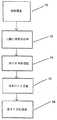
本発明の除去、洗浄および剥離方法は、図1に示されるフローチャートにより示される方法においてバッチ(多数の基板)および単一の基板操作様式のいずれにおいても有益に具体化される。本発明の方法は数工程を含み、そこでは、除去されるべき有機コーティング、フィルム、層または残留物を含有する基板をまず工程10において、三酸化硫黄と除去されるべき有機物質との反応を促進すべく、気体三酸化硫黄に暴露するのに備えるために、一つ以上の室内で物理的または化学的前処理にかける。物理的または化学的前処理には、例えば、赤外線(IR)、紫外線(UV)、またはレーザーエネルギーのような熱、高エネルギー電磁線による物理的処理;または例えば酸素、亜酸化窒素、水蒸気、蒸気相過酸化水素、窒素、または様々の溶剤を含む反応性または不反応性の気体または液体による化学的処理が含まれる。
【0027】
適切な前処理 工程10 の終了後、基板を工程12 において三酸化硫黄反応室中に配置し、気体三酸化硫黄に暴露する。本発明のいくつかの実施の形態において、前処理 工程(1 )および三酸化硫黄暴露工程(2 )を同じ物理的反応室内で行うことが都合が良い。他の実施の形態において、これらの二つの工程に多くの室が必要かもしれない。いずれにせよ、三酸化硫黄暴露工程中、従来技術に記載されているように、調節された量の気体三酸化硫黄が、連続的にまたは適切な間隔で、閉鎖した真空シールされた室内に投入され、これは三酸化硫黄暴露中の水分レベルを最小にするまたはコントロールするために主として必要とされる。水分レベルはまた、高温で室の壁を維持することによって最小にしコントロールされてもよい。三酸化硫黄ガスおよび他の処理ガスの流量および圧力、および本発明の方法における三酸化硫黄暴露に必要な暴露時間は、室のサイズおよび一度に暴露される基板の量およびそのサイズに依存する。洗浄または剥離されるべき基板の室中への導入後、窒素または通常使用される不活性ガスの一つのような乾燥不活性ガスにより、室を一度または複数回パージする。次に室を、例えば約1.33 ×10⁻¹Pa (約10−3 トル)の程度で、適切な真空に排気する。その後無水の気体三酸化硫黄を、基板上に含まれる有機コーティング、フィルム、層および残留物を除去、洗浄または剥離するための反応性試薬として室内に導入する。基板を気体三酸化硫黄および他の処理ガスに暴露する時間は多くの因子に依存して変化するのに対し、上述のように、暴露の通常の時間は5 分未満である。除去、洗浄または剥離される有機物質の性質、三酸化硫黄反応室中の基板の数、それぞれの基板のサイズ、および他の処理条件に依存して、より長い時間または反復的な暴露が必要かもしれない。しかしながら、特定の有機物質、基板、および処理条件の設定 のための時間の測定は、容易に行うことができ、不当な実験を必要としない。三酸化硫黄に暴露する間、基板は室温で維持してもよく、高温に加熱してもよい。加熱した場合、温度は本発明の方法を制限しない。基板の温度および処理環境をコントロールし、制限して本発明の方法の有効性を改善してもよい。通常、温度範囲は室温と400 ℃との間である。ここで用いたように、「室温」という用語は、処理が行われる設備の周囲の温度を称し、通常約23 ℃から約25 ℃までの範囲である。
【0028】
三酸化硫黄暴露工程中、従来技術によって開示されていないが、基板が三酸化硫黄反応室内に残留している場合には一つ以上の同時の物理的または化学的処理を行う必要があるかもしれない。同時の物理的または化学的処理には、例えば、赤外線、紫外線、レーザーエネルギーのような高エネルギー電磁線による物理的処理;三酸化硫黄反応室の物理的形状による室中の処理ガスの方向性流動;または本発明の方法の有効性を改善するために三酸化硫黄および窒素に加えて気化溶剤または亜酸化窒素のような反応性ガスを導入することによる化学的処理、が含まれる。本発明の好ましい実施の形態において、同時処理は、三酸化硫黄反応室内の三酸化硫黄の存在と正確に同時ではない。三酸化硫黄反応室内の同時の物理的または化学的処理に必要な時間調節は、有機物質の性質および有機物質が受けた一連の前の処理条件に依存する。
【0029】
三酸化硫黄工程の終了後、工程14 に示されるように、必要に応じて基板を一つ以上の室中で前すすぎ物理的または化学的処理にかけ、三酸化硫黄暴露工程後基板上に残る反応したまたは未反応の有機物質の除去を容易にしてもよい。前すすぎ物理的または化学的処理には、例えば、熱、高圧脱イオン水(DI 水)噴霧、メガソニックまたは超音波処理のような音エネルギーによる処理、レーザーエネルギーへの暴露、物理的スクラビングまたはドライアイス方法への暴露のような運動論的処理による物理的処理;または酸素、亜酸化窒素、蒸気、および蒸気相過酸化水素、または例えば様々の酸性またはアルカリ性溶液またはアミンを基剤とする溶液を含む溶液または溶剤による化学的処理が含まれる。
【0030】
必要に応じた、適切な前すすぎ物理的または化学的処理工程14 の終了後、基板を、従来技術に記載されているように、工程16 に示されるように、室中で従来のまたは標準のすすぎ処理の一つにより処理する。そのようなすすぎには、水、低級アルカノール(1 から5 までの炭素原子)、アセトン、またはそれらの混合物、様々の酸性またはアルカリ性溶液またはアミンを基剤とする溶液のようなすすぎ溶剤の使用が含まれる。工程16 のすすぎ処理中、熱、高圧脱イオン水(DI 水)噴霧による物理的処理、メガソニックまたは超音波処理のような音エネルギーによる処理またはレーザーエネルギーへの暴露のような一つ以上の物理的処理に基板を暴露してもよい。工程16 の従来のすすぎ処理の終了後、工程18 に示されるように、一つ以上の室中で一つ以上の後すすぎ物理的または化学的処理により処理し、標準すすぎ工程後に基板の表面上に残る任意の残留有機物質の除去を容易にする。後すすぎ物理的または化学的処理には、例えば、熱、赤外線(IR) 、紫外線(UV) 、またはレーザーエネルギーのような高エネルギー電磁線、高圧DI 水噴霧、メガソニックまたは超音波処理のような音エネルギーによる処理、レーザーエネルギーへの暴露、または物理的スクラビングまたはドライアイス方法への暴露のような運動論的処理による物理的処理;または酸素、亜酸化窒素、蒸気、および蒸気相過酸化水素のような様々の反応性ガス、または例えばフォトレジスト剥離に通常使用される様々の酸性またはアルカリ性溶液、コリン、またはフォトレジスト剥離に使用されるアミンを基剤とする溶液を含む溶液または溶剤による化学的処理が含まれる。
【0031】
処理工程のいずれかにおいて使用される場合、高圧DI 水噴霧は、ファンノズルまたはジュエルチップ(jewel−tip) ノズルを使用して、約350psi から約2,500psi まで、好ましくは約1,200psi の圧力下で脱イオン水により行う。所望なら、凍結点より高く沸点より低い範囲内で、冷却または加熱してもよい。
【0032】
本発明の方法は、多くの無機基板の表面またはその上の無機コーティングに有害な影響を与えない。例えば、酸化ケイ素 および酸化物 ガラス、窒化物、酸窒化物、多くの金属、珪化物、シリコン、ポリシリコン等のような表面酸化物は本発明の方法により影響を受けない。
【0033】
特定の理論に賛同せず三酸化硫黄反応の詳細と独立して、本発明の基礎をなす原理は、工程中の適切な時間において行われる適切な物理的および化学的処理と共に、溝、隙間およびすべてのマイクロメーター未満の構造を含む基板表面のすべての部分に三酸化硫黄蒸気が達することにより可能となる、有機コーティング、フィルム、層および残留物の徹底的な酸化、スルホン化、硫酸化、スルファメート化、またはそれらとの他の化学的反応である。本発明の方法は、三酸化硫黄が純粋なまたは安定化した気体の形態でも、または純粋なまたは安定化した液体、または固体の三酸化硫黄供給源から気化した形態でも実施することができる。本発明の方法は、三酸化硫黄蒸気の反応性が気体、液体、または固体形態の化学基板の混合物から得られる場合、特定の除去、洗浄または剥離反応を行うために必要な速度および量で、純粋な形態または他の形態で、三酸化硫黄蒸気を生成する正味効果を有し、等しく適用される。
【0034】
本発明のある実施の形態において、有機コーティング、フィルム、層および残留物と三酸化硫黄を含む処理ガスとの完全な反応は、例えばシリコン、ポリシリコン、ゲルマニウム、III−V族化合物 半導体(例えばヒ化 ガリウム)、酸化物(結晶およびガラス状)、窒化物、酸窒化物、有機フィルム、有機誘電体(例えばポリイミド、ベンゾシクロブテン)、有機金属複合体およびポリマー、金属および金属合金のような、半導体ウェーハーおよび装置を含む基板の表面から素早く起こる。
【0035】
従来技術において記載されていない、本発明の別の実施の形態において、基板が一部しか除去または剥離されない有機コーティング、フィルム、または層を含有する場合のように、三酸化硫黄暴露工程中において不完全な反応が所望であるかもしれない。そのような実施の形態において、適切な時間(例えば終点検出器により同定される)に処理ガスとの反応を中止させるために様々の物理的または化学的機構が必要である。反応を停止させるまたは遅くさせるための適切な機構の例には、(1 )より反応性の低いガスによる反応性の高いガスの置換のような化学的処理の実施、(2 )赤外線、紫外線(UV) 、および高エネルギー波長を含む電磁線のような、反応に影響を与える物理的処理の実施、(3 )基板の温度特性を変化させるための基板の加熱、(4 )三酸化硫黄反応室からの基板の回収、および(5 )不活性ガスによる反応性処理ガスの置換、が含まれる。
【0036】
通常、本発明の方法は、有機物質の特性を変化させ得る紫外線(UV) を含む様々の波長の電磁線への暴露、プラズマ処理への暴露、および化学的処理への暴露を含む従来の物理的および化学的処理の異なる変遷により有機コーティング、フィルム、層および残留物を除去、洗浄または剥離することができる。特に、強度のUV 、イオン注入、反応性イオンエッチング(RIE) 、乾燥および湿式エッチング、および他の厳しいプラズマ処理に暴露される残留物およびポリマーは、三酸化硫黄ガスとの反応により容易におよび効果的に除去、洗浄または剥離できる。
【0037】
本発明の方法は、マイクロメーター未満の構造の特徴が基板に加えられた場合も等しく有効である。
【0038】
有機コーティング、フィルム、層および残留物の化学的および物理的特性、並びに基板上に堆積する様式は、本発明の方法に重要ではない。有機コーティング、フィルム、層および残留物には、例えば、従来の処理活性により意図的でなく堆積されたまたはローラー加圧、浸漬、ブラッシング、噴霧、乾燥レジストのシートの使用、スピンオン(spin−on) 、電気泳動、プラズマ堆積、化学的気相成長 および有機コーティング、フィルムおよび層を使用する他の技術を含む任意の有機コーティング法により意図的に堆積された芳香族および脂肪族レジストが含まれてもよい。
【0039】
特定の除去、洗浄および剥離処理の例には、例えば、フォトレジスト剥離、BCB (ベンゾシクロブテン)剥離、後プラズマエッチング洗浄(例えば媒介洗浄、接触洗浄)、ストリンガー(stringer) ポリマー除去、金属フェンスおよびベール残留物除去、シリコンポリマー除去、硬化および不硬化ポリイミド剥離、およびポリカーボネート剥離のような有機ポリマー除去の適用が含まれる。側壁ポリマー、シリコンポリマー、ストリンガーポリマー、ベールおよび金属フェンスは、排他的 ではないが典型的に 、反応性イオンエッチング(RIE) 中形成される錯体ポリマーである。これらのポリマーおよび残留物の洗浄の困難性は、従来技術の顕著な欠点であり、本発明の方法によって克服できる。これらのポリマーには、金属、金属酸化物、エッチング剤、およびRIE の他の無機副産物が含まれてもよく、これらは酸素を基礎とするプラズマ方法(例えば乾燥灰化)、または標準すすぎ工程の後の単なる三酸化硫黄暴露工程のような従来技術によって完全に除去することが困難になる原因となる。これらのポリマーは、本発明の方法による除去、洗浄および剥離を受けやすい。これらの物質を適切に除去できないことにより、装置の収率および信頼性に負の影響を有する汚染が生じ得る。
【0040】
特定の除去、洗浄および剥離方法の他の例には、半導体装置およびウェーハー、セラミック装置、液晶表示装置、フォトマスク、フラットパネルディスプレー 、印刷回路板、印刷配線板、磁気読み/書きヘッド、薄膜読み/書きヘッド、並びに有機フィルムが堆積したかもしれない他の基板を含む様々の基板から有機コーティング、フィルム、または層を剥離する方法が含まれる。
【0041】
さらなる他の特定の例には、有機コーティング、フィルムまたは層の部分的な除去のみが必要とされている場合に、有機コーティング、フィルムまたは層を形削りする方法が含まれる。有機コーティング、フィルムまたは層の形削りは、様々の装置への誘電フィルムおよび層の組込み、および半導体装置およびウェーハー、セラミック装置、液晶表示装置、フォトマスク、フラットパネルディスプレー 、印刷回路板、印刷配線板、磁気読み/書きヘッド、薄膜読み/書きヘッド、並びに有機フィルムが堆積したかもしれない他の基板の製造および修復のための平板印刷法の改良において必要かもしれない。
【0042】
本発明により有益に処理される有機コーティング、フィルムまたは層の例には、有機誘電体が含まれる。そのような有機誘電体には、ポリイミド、コポリイミド、ポリアミド、ポリアミド−イミド、フッ素化ポリイミド、ポリ(アリーレンエーテル)、フッ素化ポリ(アリーレンエーテル)、ペルフッ素化アルキレンオキシド、パリレン(N,C,D, またはF 型) 、ポリ(フェニルキノキサリン)、ポリ−ナフタレン、ポリフッ素化ナフタレン、ベンゾシクロブテン(BCB) 、ポリテトラフルオロエチレンのような非結晶フルオロポリマー、ペルフルオロシクロブタン芳香族エーテル(PFCB) 、ポリノルボルネン、およびフッ素化炭素が含まれる。
【0043】
したがって、様々のタイプの表面から有機コーティング、フィルム、層および残留物を完全にまたは部分的に、除去、洗浄および剥離する方法が開示される。明らかな性質の様々の変化および変更が可能であり、そのような変化および変更はすべて特許請求の範囲に記載される請求項の範囲に含まれると考えられることは、当業者にとって自明である。
【図面の簡単な説明】
【図1 】本発明の方法のフローチャート[0001]
Background of the Invention
1. Field of Invention
The present invention relates to the removal, cleaning, and stripping of various organic materials deposited or formed on a substrate during manufacture, repair or regeneration of the substrate. Organic materials that are removed, washed, or stripped by the method of the present invention include, for example, photosensitive and non-photosensitive organic materials, polymerized photoresists, cured and uncured polyimides, polycarbonates, paints, resins, multilayer organic polymers, and certain organics. -Organic coatings consisting of metal complexes, positive optical photoresists, negative optical photoresists, chemically amplified photoresists, electron beam photoresists, X-ray photoresists, ion beam photoresists, and ion-implanted and other cured photoresists , Films, layers and residues may be included. These organic coatings, films, layers and residues removed by the method of the present invention include, for example, semiconductor devices and wafers, ceramic devices, liquid crystal display devices, photomasks, flat panel displays, and printed circuits. Plates, printed wiring boards, magnetic read / write heads, thin film read / write heads, and other substrates on which organic films may have been deposited may be included.
[0002]
2. Explanation of related technology
For example, photosensitive and non-photosensitive organic materials, polymerized photoresists, cured and uncured polyimides, polycarbonates, paints, resins, multilayer organic polymers, certain organic-metal complexes, positive optical photoresists, negative optical photoresists, chemicals Organic coating, film, layer and residue removal, cleaning, or stripping consisting of amplified photoresist, electron beam photoresist, x-ray photoresist, ion beam photoresist, and ion-implanted and other cured photoresists is a semiconductor device And wafers, ceramic devices, liquid crystal displays, photomasks, flat panel displays, printed circuit boards, printed wiring boards, magnetic read / write heads, thin film read / write heads, and other substrates on which organic films may have been deposited For manufacturing and regeneration This is one of the necessary steps. The removal, cleaning and stripping of such organic materials is usually (1) dry ashing or plasma ashing, dry stripping, dry etching, and kinetic methods such as abrasives, cryogenic aerosol technology, dry ice etc. (2) so-called RCA cleaning methods (developed by RCA for use in semiconductor substrate cleaning) such as sulfonic acid, hydrochloric acid, hydrogen peroxide, piranha etch ( piranha etch) (mixture of sulfonic acid and hydrogen peroxide), ozonated deionized water (DI water), and wet stripping with liquid chemicals such as ammonium hydroxide solution, and various choline solutions, amine based, for example A wet process involving the use of solutions, M-pyrrole, paint removers; and (3) often repetitive And three general techniques including a combination of drying and wet methods.
[0003]
Drying methods often involve the use of high energy ion plasma to remove organic materials (dry ashing, or plasma ashing). There are two general categories of plasma methods used. One plasma method, often referred to as barrel ashing, utilizes a plasma flow directed at the substrate. Another method, often referred to as down-stream ashing, involves the use of “downstream” (ie, physically far) of the plasma gas atmosphere from a plasma source to minimize damage to the substrate. To. Different plasma gases may be used, including gases consisting of various mixtures of oxygen, ozone, and nitrogen gases, CO 2, CO 22 And H2O 2 is produced as a final product (see, eg, Silicon Processing for the VLSI Era, Volume 1-Process Technology, S. Wolf and RN Tauber, p564, Lattice Press, Sunset Beach, 1986).
[0004]
In some cases, a hydrogen plasma may be required to assist the drying process. For example, for photoresists that are very difficult to remove, hydrogen plasma can be used to strip the top layer of the cured resist to produce a hydride that is easy to strip (eg, “Choose the Right Process to Strip”). See “Your Photoresist”, Semiconductor International, February 1990, p. 83). In other cases, residues that are difficult to remove may require the addition of fluorine gas or other halogen gas to the plasma gas mixture, or subsequent exposure to hydrofluoric acid vapor ( For example, see “Managing Etch and Implant Residue”, Semiconductor International, August 1997, p. 62).
[0005]
Many disadvantages are associated with the plasma method. These include (1) especially in the barrel asher where the crystal structure of the substrate is damaged by the impact of the substrate by the high energy ion plasma and undesired atoms in the substrate are implanted, and thus the yield of the substrate device and Radiation damage to the underlying substrate with reduced reliability (although damage may be minimized by using an anneal or downstream asher that minimizes radiation damage at the expense of slower and less efficient organic removal rates) (2) generation of additional contamination, such as high-volume ion plasma, that reacts with impurities in the resist to form an insoluble inorganic oxide that is resistant to etching (eg, “New Concerns in Dry Oxygen Ashing”, Semiconductor); International. rch 1996, p. 44); (3) contamination exacerbations commonly found in commercial photoresists such as high energy plasma drivers that cause metal impurities to be present in the substrate; (4) “via veil”; , And hardening of the sidewall polymer as a result of the formation of difficult-to-remove residues such as "metal fences" and the interaction of the plasma etch released by-products with the sidewalls in the substrate structure at high temperatures; and (5 ) Incomplete removal of photoresist and other organic material from very small features, cleaning by micromasking the resist from further processing with sputtered oxide that can be formed as a result of high energy ion bombardment And exfoliation.
[0006]
Other drying methods have been used that do not require a high energy plasma. However, these non-plasma methods typically have (1) low removal rates, (2) high temperature processing conditions, (3) such as damage from mechanical polishing caused by microsandblasting techniques such as cryogenic aerosols. Possible damage to the substrate due to excessive damage to the substrate, eg temperature fluctuations such as the dry ice method (see, for example, “Emerging Technologies; Emergence Markets”, Precision Cleaning, October 1996, p. 14), and ultraviolet radiation ( UV-irradiation), or (4) high temperature or high energy, high volume, inability to completely remove or exfoliate cured organic material by undergoing the aforementioned treatments such as ion implantation. Has as a drawback.
[0007]
Wet methods, including, for example, RCA cleaning, specialty organic solvents, acids, and oxidizing solutions such as caroic acid and other liquid reagents, also have many drawbacks when used to remove, clean, or strip organic materials. Have. These disadvantages include (1) the incomplete removal of organic matter due to the difficulty of all liquids penetrating very small features or overcoming surface tension and capillary action, (2) high Incomplete removal due to limited ability to affect certain organic materials including photoresists, photoresist residues and organo-metal complexes hardened by energy, heavy ion implantation, or high temperature processing; (3) Further occurrence of metal impurities and other residual contamination normally found in liquid reagents, (4) Contamination on all parts of the substrate, such as trace organic residues deposited in the cleaning solution, especially during the stripping process (5) many harmful or toxic properties of the required organic solvents and acids, (6) large quantities of dangerous or toxic that are often maintained in high purity conditions at high temperatures Drugs, (7) many different types of reagents to be maintained to handle different cleaning applications and process conditions immediately, (8) the difficulty and cost of safe processing of large amounts of dangerous or toxic reagents, and (9) Many liquid reagents tend to cause corrosion of the substrate, particularly when a metal film is included in the substrate.
[0008]
Normally used NH4OH / H2O2 And then HCl / H2O2 The RCA cleaning process, which is a wet process involving treatment with, has similar drawbacks that limit its effectiveness and application.
[0009]
Despite the disadvantages of these various methods of removing, cleaning and stripping organic material, there is no better method, so using drying methods combined with wet methods, which often require many iterations An acceptable level of cleanliness must be achieved when removing, cleaning and stripping organic materials that are very difficult to remove, especially cured photoresist. Curing the photoresist as a result of conventional processing is often a problem that makes removal, cleaning and stripping difficult. Photoresist curing consists of (1) high energy electromagnetic radiation and very short wavelength or intense UV irradiation, usually used in photolithographic process, which is the photoresist curing stage, and (2) high energy, high dose ion implantation. (3) a reactive ion etching process (RIE), (4) a high temperature process such as post-baking, which is a photoresist curing stage, (5) oxide, metal or polylysine dry etching, and other physical and Arising from many sources, including chemical treatments. Furthermore, dry etching and dry ashing processes often result in residues of extremely etch resistant polymers and inorganic or organometallic materials, such as sidewall polymers, veils and metal fences (eg, “What's Driving Resist Dry Stripping ", Semiconductor International, November 1994, p. 61). Under such conditions, a combined wet and dry method may be the only available technique that can provide sufficient removal, cleaning and stripping of organic material. Even under conditions where the prior art uses repeated combinations of wet methods after drying methods, certain organic materials may still be resistant to sufficient removal. For example, a photoresist that has undergone an oxide etch process leaves a fluorocarbon that is resistant to removal by continuous use of dry and wet strip processes and subsequent RCA cleaning.
[0010]
Thus, the prior art has many disadvantages that are overcome by the present invention. Such disadvantages include: (1) sidewall polymers, veils, metal fences that have undergone high energy electromagnetic radiation such as UV curing, or high energy, heavy ion implantation, or reactive ion etching (RIE). Hardened organic materials, including other inorganic residues, and photoresist removal difficulties, (2) very small features (typically less than a micron) and high aspect ratio without using plasma methods that damage the substrate Difficulty in removing organic material from features, (3) substrate damage or film erosion when plasma method must be used because there is no other effective method, (4) no other effective method Therefore, if the plasma method has to be used, a new removal-resistant inorganic substance is produced. (5) Since there is no other effective method, the plasma method is used. Exacerbation of existing contamination that can occur in the substrate if it must be, (6) additional contamination contamination when liquid reagents and solvents are used, and (7) where liquid reagents and solvent baths are used (8) Difficulty and cost to purchase, use and process large quantities of hazardous or toxic reagents and solvents, (9) Requires high frequency or microwave generators and vacuum pumps and systems (10) Difficulty in maintaining a uniform removal process across the diameter of the substrate when barrel asher is used and the stripping process must be stopped by calculating the optimum endpoint (11) The relatively high temperature (above 200 ° C.) of many drying methods that can cause problems related to certain diffusion, such as diffusion of impurities into the substrate, to become more severe ( Depending on the substrate manufacturing process used, both impurity diffusion and heat consumption may be of concern to users), (12) Expansion of the drying process to process substrates larger than 12 inches in diameter (about 30 cm) (13) Difficulty of using conventional techniques when peeling organic material from metal film without corroding the metal film, (14) Insufficient oxygen plasma for photoresist on adjacent organic film Selectivity (such as about 1: 1 selectivity exhibited by oxygen plasma when used for removal of interlayer dielectric film material, photoresist adjacent to BCB), and (15) hardened organic material from the substrate There is a frequent need to develop and implement complex and expensive multi-step, dry and wet removal methods for proper cleaning.
[0011]
Issued on August 6, 1991. U.S. Pat. No. 5,037,506 entitled “Method for Stripping Organic Layers” by Gupta et al describes the use of gaseous sulfur trioxide followed by a solvent rinse during the manufacture of semiconductor or ceramic devices. Discloses and claims a two-step method for removing various organic coatings, polymerized photoresists, and in particular the cast layer and the strong UV cured resist layer. Although the method disclosed and claimed in this patent is useful, there is a further need to clean the surface and remove organic matter that extends to other areas of technology not disclosed or claimed in this patent. In particular, the undisclosed and unclaimed needs include not only semiconductor devices, wafers, ceramic devices and printed circuit boards considered in the prior art, but also liquid crystal display devices, photomasks, flat panel displays, printed wiring boards, There is a need to remove, clean, and strip organic materials contained on various substrates, including magnetic read / write heads, thin film read / write heads, and other substrates on which organic films may have been deposited, (1) Inadequate liquid stripping and cleaning methods due to surface tension and capillary action, or contamination introduced and diffused by liquids, (2) Substrate damage, erosion, or incomplete organometallic damage due to plasma technology (3) Improved uniformity of removal method across the diameter or larger dimensions of the substrate provided by the prior art (4) it is necessary to remove organic material at a faster throughput than provided by the prior art by providing (4) inherently faster organic removal rates or by providing very large batch throughput; (5) More effective removal of silicon polymers, sidewall polymers, veils, metal fences, and other inorganic residues resulting from dry etching methods is required, and (6) hazardous or toxic and other liquid waste There is a need for an integrated method of cleaning organic and inorganic residues using a minimum of (7) minimizing or eliminating erosion of the substrate metal film during organic cleaning (8) ) It is necessary to integrate steps in the stripping and cleaning process to improve cycle time, working process, and throughput, and (9) process temperature must be minimized. And (10) an organic coating, for example required when trying to flatten or form a coating, or to remove one organic coating from an underlying organic coating with great selectivity, Included is the need to include the feature that removal or peeling of only a portion of the film or layer is required.
[0012]
As a result of the passage of time, it has become apparent to the inventors that further consideration is required regarding the method of the above-mentioned patent in order to improve the effectiveness of the method. As noted herein, the effectiveness of the method of the present invention refers to the integrity of the organic removal method, the elimination of substrate damage and erosion, improved uniformity of processing on the substrate, faster organic removal rate and substrate throughput. , Increasing the number of substrates that can be processed simultaneously in one processing cycle, minimizing substrate erosion, minimizing total liquid waste generated by the method of the present invention, minimizing hazardous or toxic chemical usage Means improved selectivity of minimizing the total process cycle time, minimizing process temperature requirements, and removal of the first type of organic coating proximate to the second type of organic coating. These further considerations may require (1) chemical or physical pretreatment of organic materials and substrates before the substrate is inserted into the sulfur trioxide reaction chamber and exposed to the process gas, (2) As specified in the prior art, it may also be necessary to mix a reactive treatment gas other than inert gas, dry nitrogen or sulfur trioxide with sulfur trioxide in a sulfur trioxide reaction chamber, (3) It may be necessary to introduce a reactive treatment gas other than sulfur trioxide into the sulfur trioxide reaction chamber in a specific order before or after the introduction of sulfur oxide. (4) Any one of the treatment gases It may be necessary to fill the sulfur trioxide reaction chamber at regular intervals during the process of the invention. (5) During the process of the present invention, it is necessary to flow all process gases in the sulfur trioxide reaction chamber. There may be and the flow is (6) in the sulfur trioxide reaction chamber, the process gas and substrate temperature may need to follow a time-temperature curve, (7) the sulfur trioxide reaction chamber The partial pressure of the processing gas in it may also need to follow a partial pressure vs. time curve, (8) Simultaneous physical processing of the substrate (eg high energy electromagnetic radiation such as ultraviolet light) is processed in the exposure chamber May be necessary during gas exposure, (9) may need to stop the treatment reaction in the sulfur trioxide reaction chamber at an exact time before termination, (10) treatment in the sulfur trioxide reaction chamber It may be necessary to pre-rinse chemical or physical treatment of the substrate after exposure to the gas but before rinsing the reaction product in solution, (11) eg ultrasonic or megasonic. ) The use of simultaneous physical processing, such as processing, or various other kinetic methods may be necessary in rinsing the substrate in solution as described in the prior art to remove reaction products, and (12) Rinsing the substrate in solution may include chemical or physical treatments that may be post-rinsed after removal of reaction products.
[0013]
What is needed is, for example, semiconductor devices and wafers, ceramic devices, liquid crystal displays, photomasks, flat panel displays, printed circuit boards, printed wiring boards, magnetic read / write heads, thin film read / write heads, and organic on a substrate From various substrates, including other substrates on which films may have been deposited, eg photosensitive and non-photosensitive organic materials, polymerized photoresists, cured and uncured polyimides, polycarbonates, paints, resins, multilayer organic polymers, certain organometallics Organic coatings, films consisting of composites, positive optical photoresists, negative optical photoresists, chemically amplified photoresists, electron beam photoresists, X-ray photoresists, ion beam photoresists, and ion-implanted and other cured photoresists , Layer and residue Effective removal of a method to satisfy these considerations about peeling or washing.
[0014]
Summary of the Invention
Accordingly, the object of the present invention is, for example, semiconductor devices and wafers, ceramic devices, liquid crystal display devices, photomasks, flat panel displays, printed circuit boards, printed wiring boards, magnetic read / write heads, thin film read / write heads, and organic From various substrates, including other substrates on which films may have been deposited, eg photosensitive and non-photosensitive organic materials, polymerized photoresists, cured and uncured polyimides, polycarbonates, paints, resins, multilayer organic polymers, certain organometallics Organic coatings, films consisting of composites, positive optical photoresists, negative optical photoresists, chemically amplified photoresists, electron beam photoresists, X-ray photoresists, ion beam photoresists, and ion-implanted and other cured photoresists , Layer and The residue was completely removed, a cleaning and a method for peeling,
(1) Do not use liquid stripping or cleaning reagents containing, for example, organic and inorganic solvents and acids,
(2) without using plasma methods including, for example, dry ashing, barrel ashing, or downstream ashing,
(3) It is effective to completely remove, wash, or peel off some organic substances at a processing temperature of 200 ° C. or lower,
(4) Provide substrate removal, cleaning, or stripping with better uniformity than can be provided by plasma stripping or cleaning methods that require endpoint detection to measure the optimal time to stop processing;
(5) Provides more uniform removal, cleaning, or stripping between each processed substrate than can be provided by plasma stripping or cleaning methods that require endpoint detection to measure the optimal time to stop processing. And
(6) provide improved selectivity of removal between two different types of organic films that can be in close proximity as in the case of organic photoresists and organic interlayer dielectric films;
(7) Effectively embodied as part of an integrated cleaning method for cleaning and removing inorganic and organic materials,
It is to provide a method.
[0015]
In accordance with the present invention, a method is provided for partially or completely removing an organic coating, film, layer or residue from a substrate. The method of the present invention includes:
(A) subjecting the organic coating, film, layer, or residue to chemical or physical pretreatment;
(B) exposing the organic coating, film, layer, or residue to a vapor consisting essentially of anhydrous gaseous sulfur trioxide for a period of time to maintain the substrate at a temperature ranging from room temperature to about 400 ° C;
(C) subjecting the organic coating, film, layer, or residue to a pre-rinse chemical or physical treatment, as appropriate,
(D) Rinse the organic coating, film, layer, or residue with a solvent,
(E) subjecting the organic coating, film, layer, or residue to a chemical or physical post-rinse treatment;
Each step is included.
[0016]
Sulfur trioxide, which acts as a removal, cleaning, and stripping agent, reacts in oxidation, sulphonation, sulphation, sulphamatation, or otherwise, such as photosensitive and non-photosensitive organic materials, polymerized photoresists, curing and Uncured polyimide, polycarbonate, paint, resin, multilayer organic polymer, certain organometallic composites, positive optical photoresist, negative optical photoresist, chemically amplified photoresist, electron beam photoresist, X-ray photoresist, ion beam photo All types of resist, and organic coatings, films, layers and residues consisting of ion implantation and other cured photoresists are made substantially completely removable by subsequent chemical or physical processing.
[0017]
After preparing the sulfur trioxide reaction chamber for use by first filling it with an inert gas, the substrate on which the organic coatings, films, layers, and residues were deposited, regardless of the method of deposition, was adjusted to a controlled amount of gas. Exposure to sulfur trioxide and other process gases. These gases are injected with good vacuum strength into the chamber containing the substrate or into a series of closed chambers. To improve the effectiveness of this method, additional chemical and physical treatments are performed before, during and after exposure to these process gases. Store liquid or solid sulfur trioxide in alpha, beta, or gamma form, or a mixture thereof, and use it as a source of vapor. Sulfur trioxide is a very strong oxidizing and sulfonated chemical and is very effective as a drug in the removal, cleaning and stripping of various organic materials. Sulfur trioxide gas is particularly effective as a chemical in the removal, cleaning and stripping of organic materials such as plasma cured photoresists, fluorocarbon-containing polymers, UV cured photoresists, and sidewall polymers from sub-micrometer grooves and gaps It is. When in the gas phase, sulfur trioxide can make more complete contact with submicrometer grooves and interstices than is possible with liquid solutions.
[0018]
The inventive method of removing, cleaning, or stripping various organic materials deposited or formed on a substrate during substrate manufacture, repair, or regeneration may be performed at a temperature range that is not limited with respect to the effectiveness of the method. However, in some embodiments of the invention, temperatures ranging from room temperature to 400 ° C. are required for optimal effectiveness for specific materials and substrates.
[0019]
Examples of substrate materials that are beneficially treated according to the present invention include silicon, polysilicon, germanium, III-V compound semiconductors (eg, gallium magnets), oxides (crystalline and glassy), nitrides, oxynitrides Includes materials specifically used in the manufacture and repair of semiconductor wafers and equipment, such as organic films, organic dielectrics (eg polyimide, benzocyclobutene), organometallic composites and polymers, metals and metal alloys It is.
[0020]
Additional examples of substrate materials that are beneficially treated according to the present invention include materials such as glass, polycarbonate, and cured and uncured polyimide.
[0021]
By using organic removal, cleaning and stripping methods for sulfur trioxide as described in the present invention, semiconductor devices and wafers, ceramic devices, liquid crystal display devices, photomasks, flat panel displays, printed circuit boards, printed wiring boards A more effective, more effective and more environmentally friendly treatment of magnetic read / write heads, thin film read / write heads and other substrates on which organic films are deposited and contain very small features is provided.
[0022]
Detailed Description of the Invention
The details of certain embodiments of the invention are set forth in order to illustrate the best mode presently contemplated by the inventors for carrying out the invention. Alternative embodiments are also briefly described as applicable.
[0023]
Semiconductor devices and wafers, ceramic devices, liquid crystal displays, photomasks, flat panel displays, printed circuit boards, as a result of intentional or unintentional chemical and physical methods necessary for manufacturing and repair, Printed wiring boards, magnetic read / write heads, thin film read / write heads, and other substrates on which organic films may be deposited, such as photosensitive and non-photosensitive organic materials, polymerized photoresists, curing and Uncured polyimide, polycarbonate, paint, resin, multilayer organic polymer, certain organometallic composites, positive optical photoresist, negative optical photoresist, chemically amplified photoresist, electron beam photoresist, X-ray photoresist, ion beam photo Resist, and ion implantation and others Organic coating comprising a cured photoresist film, removing the layers and residues, cleaning, or a method for peeling was developed designed.
[0024]
The basic concept of the present invention is new when used with the appropriate physical and chemical treatments used under the proper treatment conditions and at the appropriate time during the treatment and contains substantially sulfur trioxide. A chemical agent is used in gaseous form to oxidize, sulfonate, sulfate, sulfamate, or otherwise react various organic materials that can be deposited or formed on the substrate during manufacture, repair or regeneration of the substrate, That is, the desired organic material can be substantially removed, cleaned, or stripped from the surface of the substrate. Sulfur trioxide, a highly reactive agent, is very effective in removing, cleaning and stripping various hardened organic materials. The gaseous form of sulfur trioxide is also an agent that, in combination with reactive power, removes, cleans and strips various organic materials from sub-micrometer grooves and gaps of exposed substrates very effectively. When in the gas phase, sulfur trioxide does not suffer from surface tension and capillary action that limit the action of the liquid solution by preventing contact with such grooves and gaps. The present invention therefore (1) applies organic coatings, films, layers and residues to the grooves by applying very strong reactive reagents to very small grooves and gaps that cannot be easily reached by liquid reagents. And methods for substantially removing, cleaning or stripping from gaps; (2) methods for removing, cleaning and stripping organic coatings, films, layers and residues without the use of large amounts of dangerous or toxic solvents and reagents; (3) A method for removing, washing and stripping organic coatings, films, layers and residues, effective between room temperature and 200 ° C .; (4) Organic, which can be easily integrated into inorganic cleaning and stripping methods A method of removing, cleaning and stripping coatings, films, layers and residues; (5) organic coatings, films and uniformly across the substrate; (6) a method for selectively and completely removing organic coatings, films and layers without damaging organic coatings of different types that may be in close proximity; and (7 ) To provide a method for partially or completely removing organic coatings, films and layers uniformly between each treated substrate;
[0025]
In the method of the present invention, sulfur trioxide, which may be in alpha form, beta form, gamma form or a mixture thereof, is stored and used as an oxidizing, sulfonated, sulfated, sulfaminated or other reactive reagent. Gamma-sulfur trioxide, which has a melting point of 16.8 ° C., is the preferred form for the sulfur trioxide used in the present invention and is SO when it is maintained under completely pure anhydrous conditions.3 Is an inherent form. Usually, stabilized gamma-sulfur trioxide is used and the addition of a small amount of inhibitor (stabilizer) prevents the formation of high melting beta (32.5 ° C.) and alpha (62.3 ° C.) forms. Gamma-sulfur trioxide is commercially available with such inhibitors. Stabilized sulfur trioxide can be easily redissolved when solidified. Stabilized and unstabilized sulfur trioxide may be used in the process of the present invention. Anhydrous, gaseous sulfur trioxide is used for removal of organic coatings, films, layers and residues. Eliminating or minimizing the introduction of water or water vapor into the sulfur trioxide gas at the appropriate time of the invention and controlling moisture during the process of the invention is an important requirement of the method of the invention. The presence of water during exposure to sulfur trioxide gas reduces the effectiveness of the method of the present invention.
[0026]
The removal, cleaning and stripping method of the present invention is beneficially embodied in both the batch (multiple substrates) and single substrate operating modes in the method illustrated by the flowchart shown in FIG. The method of the present invention involves several steps in which the substrate containing the organic coating, film, layer or residue to be removed is first reacted in
[0027]
After completion of the
[0028]
While not disclosed by the prior art during the sulfur trioxide exposure process, it may be necessary to perform one or more simultaneous physical or chemical treatments if the substrate remains in the sulfur trioxide reaction chamber. Absent. Simultaneous physical or chemical treatment includes, for example, physical treatment with high energy electromagnetic radiation such as infrared, ultraviolet, laser energy; directional flow of process gas in the chamber due to the physical shape of the sulfur trioxide reaction chamber Or chemical treatment by introducing a reactive gas such as a vaporized solvent or nitrous oxide in addition to sulfur trioxide and nitrogen to improve the effectiveness of the process of the present invention. In a preferred embodiment of the invention, the simultaneous treatment is not exactly coincident with the presence of sulfur trioxide in the sulfur trioxide reaction chamber. The time adjustment required for simultaneous physical or chemical treatment in the sulfur trioxide reaction chamber depends on the nature of the organic material and the series of previous treatment conditions experienced by the organic material.
[0029]
After completion of the sulfur trioxide process, as shown in
[0030]
After completion of the appropriate pre-rinse physical or
[0031]
When used in any of the processing steps, the high pressure DI water spray is a pressure from about 350 psi to about 2500 psi, preferably about 1200 psi using a fan nozzle or a jewel-tip nozzle. Under deionized water. If desired, it may be cooled or heated in the range above the freezing point and below the boiling point.
[0032]
The method of the present invention does not deleteriously affect the surface of many inorganic substrates or inorganic coatings thereon. For example, surface oxides such as silicon oxide and oxide glasses, nitrides, oxynitrides, many metals, silicides, silicon, polysilicon, etc. are not affected by the method of the present invention.
[0033]
Independent of the details of the sulfur trioxide reaction, which is not in favor of any particular theory, the principle underlying the present invention is that the grooves, gaps and gaps, along with appropriate physical and chemical treatments performed at the appropriate time in the process. Thorough oxidation, sulfonation, sulfation, and sulfamate of organic coatings, films, layers, and residues made possible by sulfur trioxide vapor reaching all parts of the substrate surface, including all sub-micrometer structures Or other chemical reaction with them. The process of the invention can be carried out in the form of sulfur trioxide in pure or stabilized gas form or vaporized from a pure or stabilized liquid or solid sulfur trioxide source. The method of the present invention provides the rate and amount required to perform a specific removal, cleaning or stripping reaction when the reactivity of the sulfur trioxide vapor is obtained from a mixture of chemical substrates in gaseous, liquid or solid form. Has the net effect of producing sulfur trioxide vapor in pure form or other forms and applies equally.
[0034]
In certain embodiments of the present invention, the complete reaction of organic coatings, films, layers, and residues with a process gas containing sulfur trioxide can be achieved by, for example, silicon, polysilicon, germanium, III-V compound semiconductors (eg, Gallium oxide), oxides (crystalline and glassy), nitrides, oxynitrides, organic films, organic dielectrics (eg polyimide, benzocyclobutene), organometallic composites and polymers, metals and metal alloys, It happens quickly from the surface of the substrate containing semiconductor wafers and equipment.
[0035]
In another embodiment of the present invention that has not been described in the prior art, during the sulfur trioxide exposure step, such as when the substrate contains an organic coating, film, or layer that is only partially removed or stripped. A complete reaction may be desired. In such embodiments, various physical or chemical mechanisms are required to stop the reaction with the process gas at an appropriate time (eg, identified by an endpoint detector). Examples of suitable mechanisms for stopping or slowing the reaction include (1) performing a chemical treatment such as replacement of a more reactive gas with a less reactive gas, (2) infrared, ultraviolet ( UV), and physical treatments that affect the reaction, such as electromagnetic radiation including high energy wavelengths, (3) heating of the substrate to change the temperature characteristics of the substrate, (4) sulfur trioxide reaction chamber Recovery of the substrate from (5) and replacement of the reactive processing gas with an inert gas.
[0036]
In general, the methods of the present invention involve conventional physics, including exposure to various wavelengths of electromagnetic radiation, including ultraviolet (UV), which can alter the properties of organic materials, exposure to plasma treatment, and exposure to chemical treatment. Organic coatings, films, layers and residues can be removed, washed or stripped by different transitions in chemical and chemical processes. In particular, residues and polymers exposed to intense UV, ion implantation, reactive ion etching (RIE), dry and wet etching, and other harsh plasma treatments are easily and effectively affected by reaction with sulfur trioxide gas. Can be removed, washed or stripped.
[0037]
The method of the present invention is equally effective when sub-micrometer structural features are added to the substrate.
[0038]
The chemical and physical properties of organic coatings, films, layers and residues, and the manner in which they are deposited on the substrate are not critical to the method of the present invention. For organic coatings, films, layers and residues, for example, unintentionally deposited by conventional processing activities or roller pressing, dipping, brushing, spraying, using dry resist sheets, spin-on Including aromatic and aliphatic resists intentionally deposited by any organic coating method, including electrophoresis, plasma deposition, chemical vapor deposition and other techniques using organic coatings, films and layers Good.
[0039]
Examples of specific removal, cleaning and stripping processes include, for example, photoresist stripping, BCB (benzocyclobutene) stripping, post-plasma etch cleaning (eg mediated cleaning, contact cleaning), stringer polymer removal, metal fences and Application of organic polymer removal such as veil residue removal, silicon polymer removal, cured and uncured polyimide stripping, and polycarbonate stripping is included. Sidewall polymers, silicon polymers, stringer polymers, veils and metal fences are typically, but not exclusively, complex polymers formed during reactive ion etching (RIE). The difficulty in cleaning these polymers and residues is a significant disadvantage of the prior art and can be overcome by the method of the present invention. These polymers may include metals, metal oxides, etchants, and other inorganic by-products of RIE, such as oxygen-based plasma methods (eg, dry ashing), or standard rinse processes. It can be difficult to remove completely by conventional techniques such as a subsequent simple sulfur trioxide exposure step. These polymers are susceptible to removal, cleaning and stripping by the method of the present invention. Failure to properly remove these materials can result in contamination that has a negative impact on equipment yield and reliability.
[0040]
Other examples of specific removal, cleaning and stripping methods include semiconductor devices and wafers, ceramic devices, liquid crystal displays, photomasks, flat panel displays, printed circuit boards, printed wiring boards, magnetic read / write heads, thin film readings. Included are methods for peeling organic coatings, films, or layers from a variety of substrates, including / other heads on which organic films may have been deposited.
[0041]
Yet another specific example includes a method of shaping an organic coating, film or layer where only partial removal of the organic coating, film or layer is required. Organic coating, film or layer shaping, incorporation of dielectric films and layers into various devices, and semiconductor devices and wafers, ceramic devices, liquid crystal displays, photomasks, flat panel displays, printed circuit boards, printed wiring boards May be necessary in improving lithographic printing methods for the manufacture and repair of magnetic read / write heads, thin film read / write heads, and other substrates on which organic films may have been deposited.
[0042]
Examples of organic coatings, films or layers that are beneficially treated according to the present invention include organic dielectrics. Such organic dielectrics include polyimide, copolyimide, polyamide, polyamide-imide, fluorinated polyimide, poly (arylene ether), fluorinated poly (arylene ether), perfluorinated alkylene oxide, parylene (N, C, D, or F type), poly (phenylquinoxaline), poly-naphthalene, polyfluorinated naphthalene, benzocyclobutene (BCB), amorphous fluoropolymers such as polytetrafluoroethylene, perfluorocyclobutane aromatic ether (PFCB), Polynorbornene and fluorinated carbon are included.
[0043]
Accordingly, a method for completely or partially removing, cleaning and stripping organic coatings, films, layers and residues from various types of surfaces is disclosed. It will be apparent to those skilled in the art that various changes and modifications in obvious nature are possible, and all such changes and modifications are considered to be within the scope of the claims recited in the claims.
[Brief description of the drawings]
FIG. 1 is a flowchart of the method of the present invention.
Claims (12)
Translated fromJapanese(a)前記有機コーティング、フィルム、層、または残留物を、無水気体三酸化硫黄と除去すべき前記有機コーティング、フィルム、層、または残留物との反応を促進すべく化学的または物理的前処理にかけ、
(b)前記有機コーティング、フィルム、層、または残留物を一定の時間、無水気体三酸化硫黄から実質的になる蒸気に暴露し、前記基板を室温から約400℃までの範囲の温度に維持し、
(c)前記有機コーティング、フィルム、層、または残留物を溶剤ですすぎ、
(d)前記有機コーティング、フィルム、層、または残留物を化学的または物理的後すすぎ処理にかける、
各工程を含むことを特徴とする方法。A method for partially or completely removing an organic coating, film, layer or residue from a substrate, comprising:
(a) a chemical or physical pretreatment to promote the reaction of the organic coating, film, layer, or residue with anhydrous gaseous sulfur trioxide to be removed with the organic coating, film, layer, or residue To
(b) exposing the organic coating, film, layer, or residue to a vapor consisting essentially of anhydrous gaseous sulfur trioxide for a period of time to maintain the substrate at a temperature ranging from room temperature to about 400 ° C. ,
(c) rinsing the organic coating, film, layer, or residue with a solvent;
(d) subjecting the organic coating, film, layer, or residue to a chemical or physical post-rinse treatment;
A method comprising each step.
(b)前記基板を室中に配置し、
(c)前記室を乾燥不活性ガスでパージし、
(d)無水気体三酸化硫黄から実質的になる前記蒸気を前記室に導入し、前記コーティング、フィルム、層、または残留物と反応させ、
(e)適切な時間を経過させて前記三酸化硫黄と前記コーティング、フィルム、層、または残留物とを反応させ、
(f)前記三酸化硫黄と前記コーティング、フィルム、層、または残留物との前記反応を、前記基板を終点化学的または終点物理的処理をすることにより終了させる、
各工程を含むことを特徴とする請求項1記載の方法。(a) treating the substrate by the chemical or physical pretreatment;
(b) placing the substrate in a chamber;
(c) purging the chamber with dry inert gas;
(d) introducing the vapor consisting essentially of anhydrous gaseous sulfur trioxide into the chamber to react with the coating, film, layer or residue;
(e) reacting the sulfur trioxide with the coating, film, layer or residue over an appropriate period of time;
(f) terminating the reaction of the sulfur trioxide with the coating, film, layer, or residue by subjecting the substrate to an endpoint chemical or endpoint physical treatment;
The method of claim 1, comprising each step.
Applications Claiming Priority (3)
| Application Number | Priority Date | Filing Date | Title |
|---|---|---|---|
| US14144398A | 1998-08-27 | 1998-08-27 | |
| US09/141,443 | 1998-08-27 | ||
| PCT/US1999/019018WO2000012231A1 (en) | 1998-08-27 | 1999-08-20 | Method of removing organic materials from substrates |
Publications (2)
| Publication Number | Publication Date |
|---|---|
| JP2002523906A JP2002523906A (en) | 2002-07-30 |
| JP3611196B2true JP3611196B2 (en) | 2005-01-19 |
Family
ID=22495715
Family Applications (1)
| Application Number | Title | Priority Date | Filing Date |
|---|---|---|---|
| JP2000567319AExpired - Fee RelatedJP3611196B2 (en) | 1998-08-27 | 1999-08-20 | Method for removing organic material from a substrate |
Country Status (10)
| Country | Link |
|---|---|
| EP (1) | EP1123166B1 (en) |
| JP (1) | JP3611196B2 (en) |
| KR (1) | KR100391526B1 (en) |
| CN (1) | CN1234472C (en) |
| AT (1) | ATE347454T1 (en) |
| CA (1) | CA2341548C (en) |
| DE (1) | DE69934326T2 (en) |
| IL (1) | IL141595A0 (en) |
| MY (1) | MY125913A (en) |
| WO (1) | WO2000012231A1 (en) |
Families Citing this family (18)
| Publication number | Priority date | Publication date | Assignee | Title |
|---|---|---|---|---|
| JP3522249B2 (en) | 2000-10-25 | 2004-04-26 | 鹿児島日本電気株式会社 | Organic film peeling method |
| US6554004B1 (en) | 2000-11-07 | 2003-04-29 | Motorola, Inc. | Method for removing etch residue resulting from a process for forming a via |
| US6756187B2 (en) | 2002-01-04 | 2004-06-29 | Nec Lcd Technologies, Ltd. | Method for removing patterned layer from lower layer through reflow |
| JP4979941B2 (en)* | 2005-03-30 | 2012-07-18 | Hoya株式会社 | Manufacturing method of glass substrate for mask blanks, manufacturing method of mask blanks |
| US8034189B2 (en)* | 2005-05-02 | 2011-10-11 | Nalco Company | Processes for surface cleaning |
| KR20080051961A (en) | 2006-12-07 | 2008-06-11 | 한국전자통신연구원 | Cleaning Method of Flexible Substrate |
| JP5151297B2 (en)* | 2007-07-27 | 2013-02-27 | 宇部興産株式会社 | Manufacturing method of resin film, manufacturing method of conductive layer laminated resin film |
| EP2399680A1 (en)* | 2007-07-31 | 2011-12-28 | Corning Incorporated | DUV optic |
| KR100912704B1 (en)* | 2008-04-22 | 2009-08-19 | 세메스 주식회사 | Substrate Processing Apparatus and Photoresist Removal Method |
| CN104779178B (en)* | 2014-01-13 | 2018-10-16 | 中芯国际集成电路制造(上海)有限公司 | Bottom anti-reflective layer forming method |
| TWI528070B (en)* | 2014-04-18 | 2016-04-01 | 遠東科技大學 | Method of removing the polymer film of LCD module by microwave heating |
| CN104117501A (en)* | 2014-06-26 | 2014-10-29 | 苏州一合光学有限公司 | Tank arrangement structure of ultrasonic washing unit |
| KR102134261B1 (en)* | 2018-10-25 | 2020-07-16 | 세메스 주식회사 | Apparatus and method for processing substrate |
| WO2020210660A1 (en) | 2019-04-12 | 2020-10-15 | Inpria Corporation | Organometallic photoresist developer compositions and processing methods |
| CN109898089A (en)* | 2019-04-26 | 2019-06-18 | 宁德阿李科技有限公司 | A kind of surface of aluminum plate processing method |
| JP2023515693A (en)* | 2020-03-02 | 2023-04-13 | インプリア・コーポレイション | Process environment for inorganic resist patterning |
| JP7186751B2 (en)* | 2020-08-28 | 2022-12-09 | 野村マイクロ・サイエンス株式会社 | Resist Stripping Method, Resist Stripping Apparatus, and Pretreatment Method |
| CN115846310A (en)* | 2022-12-23 | 2023-03-28 | 上海华源磁业股份有限公司 | Magnetic ferrite core surface coating cleaning process |
Family Cites Families (5)
| Publication number | Priority date | Publication date | Assignee | Title |
|---|---|---|---|---|
| US4363673A (en)* | 1981-05-22 | 1982-12-14 | The Dow Chemical Company | Process for the removal of carbon from solid surfaces |
| WO1989000895A1 (en)* | 1987-07-29 | 1989-02-09 | Purusar Corporation | Surface treatment to remove impurities in microrecesses |
| US5037506A (en)* | 1990-09-06 | 1991-08-06 | Subhash Gupta | Method of stripping layers of organic materials |
| US5227001A (en)* | 1990-10-19 | 1993-07-13 | Integrated Process Equipment Corporation | Integrated dry-wet semiconductor layer removal apparatus and method |
| US5763016A (en)* | 1996-12-19 | 1998-06-09 | Anon, Incorporated | Method of forming patterns in organic coatings films and layers |
- 1999
- 1999-08-20CNCNB99812642XApatent/CN1234472C/ennot_activeExpired - Fee Related
- 1999-08-20EPEP99943798Apatent/EP1123166B1/ennot_activeExpired - Lifetime
- 1999-08-20CACA002341548Apatent/CA2341548C/ennot_activeExpired - Fee Related
- 1999-08-20ILIL14159599Apatent/IL141595A0/ennot_activeIP Right Cessation
- 1999-08-20ATAT99943798Tpatent/ATE347454T1/ennot_activeIP Right Cessation
- 1999-08-20KRKR10-2001-7002470Apatent/KR100391526B1/ennot_activeExpired - Fee Related
- 1999-08-20DEDE69934326Tpatent/DE69934326T2/ennot_activeExpired - Lifetime
- 1999-08-20JPJP2000567319Apatent/JP3611196B2/ennot_activeExpired - Fee Related
- 1999-08-20WOPCT/US1999/019018patent/WO2000012231A1/enactiveIP Right Grant
- 1999-08-26MYMYPI99003662Apatent/MY125913A/enunknown
Also Published As
| Publication number | Publication date |
|---|---|
| ATE347454T1 (en) | 2006-12-15 |
| CN1359316A (en) | 2002-07-17 |
| KR100391526B1 (en) | 2003-07-12 |
| EP1123166A4 (en) | 2003-08-06 |
| DE69934326T2 (en) | 2007-06-21 |
| EP1123166A1 (en) | 2001-08-16 |
| DE69934326D1 (en) | 2007-01-18 |
| JP2002523906A (en) | 2002-07-30 |
| KR20010109267A (en) | 2001-12-08 |
| CA2341548A1 (en) | 2000-03-09 |
| WO2000012231A1 (en) | 2000-03-09 |
| EP1123166B1 (en) | 2006-12-06 |
| CN1234472C (en) | 2006-01-04 |
| IL141595A0 (en) | 2002-03-10 |
| MY125913A (en) | 2006-08-30 |
| CA2341548C (en) | 2006-12-19 |
Similar Documents
| Publication | Publication Date | Title |
|---|---|---|
| US8066819B2 (en) | Method of removing organic materials from substrates | |
| JP3611196B2 (en) | Method for removing organic material from a substrate | |
| US5037506A (en) | Method of stripping layers of organic materials | |
| CN1481519A (en) | Process for removal of photoresis after post ion implantation | |
| KR100519835B1 (en) | Film forming method, and semi-conductor device, electric circuit, display module, color filter and light emitting element produced by the techniques | |
| US20080299780A1 (en) | Method and apparatus for laser oxidation and reduction | |
| KR20040105567A (en) | Method and apparatus for removing organic layers | |
| JP5770740B2 (en) | Method and apparatus for improving the passivation process to protect silicon prior to high dose implant strips | |
| US20060151007A1 (en) | Workpiece processing using ozone gas and chelating agents | |
| JP4031440B2 (en) | Contaminant removal using supercritical processing | |
| US5792275A (en) | Film removal by chemical transformation and aerosol clean | |
| US6184134B1 (en) | Dry process for cleaning residues/polymers after metal etch | |
| TWI497235B (en) | High dose implantation strip (hdis) in h2 base chemistry | |
| JPH08153710A (en) | Method for manufacturing semiconductor device | |
| KR20030010754A (en) | Plasma rie polymer removal | |
| KR100277781B1 (en) | Method for manufacturing semiconductor device | |
| JP2009513015A (en) | Non-plasma method to remove photoresist from substrate | |
| TW200524032A (en) | Substrate processing method, substrate processing apparatus and computer-readable recording medium | |
| US20010050272A1 (en) | Laser removal of foreign materials from surfaces | |
| US7524383B2 (en) | Method and system for passivating a processing chamber | |
| EP1032026B1 (en) | Method of photoresist ash residue removal | |
| JP4299638B2 (en) | Substrate processing apparatus and substrate processing method | |
| US20080060682A1 (en) | High temperature spm treatment for photoresist stripping | |
| US20040040934A1 (en) | Method of etching a photoresist layer disposed on a semiconductor substrate | |
| JPH0927473A (en) | Method and apparatus for removing resist |
Legal Events
| Date | Code | Title | Description |
|---|---|---|---|
| TRDD | Decision of grant or rejection written | ||
| A01 | Written decision to grant a patent or to grant a registration (utility model) | Free format text:JAPANESE INTERMEDIATE CODE: A01 Effective date:20040914 | |
| A61 | First payment of annual fees (during grant procedure) | Free format text:JAPANESE INTERMEDIATE CODE: A61 Effective date:20041014 | |
| R150 | Certificate of patent or registration of utility model | Free format text:JAPANESE INTERMEDIATE CODE: R150 | |
| FPAY | Renewal fee payment (event date is renewal date of database) | Free format text:PAYMENT UNTIL: 20081029 Year of fee payment:4 | |
| FPAY | Renewal fee payment (event date is renewal date of database) | Free format text:PAYMENT UNTIL: 20081029 Year of fee payment:4 | |
| FPAY | Renewal fee payment (event date is renewal date of database) | Free format text:PAYMENT UNTIL: 20091029 Year of fee payment:5 | |
| FPAY | Renewal fee payment (event date is renewal date of database) | Free format text:PAYMENT UNTIL: 20101029 Year of fee payment:6 | |
| FPAY | Renewal fee payment (event date is renewal date of database) | Free format text:PAYMENT UNTIL: 20101029 Year of fee payment:6 | |
| FPAY | Renewal fee payment (event date is renewal date of database) | Free format text:PAYMENT UNTIL: 20111029 Year of fee payment:7 | |
| FPAY | Renewal fee payment (event date is renewal date of database) | Free format text:PAYMENT UNTIL: 20111029 Year of fee payment:7 | |
| FPAY | Renewal fee payment (event date is renewal date of database) | Free format text:PAYMENT UNTIL: 20121029 Year of fee payment:8 | |
| FPAY | Renewal fee payment (event date is renewal date of database) | Free format text:PAYMENT UNTIL: 20131029 Year of fee payment:9 | |
| R250 | Receipt of annual fees | Free format text:JAPANESE INTERMEDIATE CODE: R250 | |
| R250 | Receipt of annual fees | Free format text:JAPANESE INTERMEDIATE CODE: R250 | |
| R250 | Receipt of annual fees | Free format text:JAPANESE INTERMEDIATE CODE: R250 | |
| LAPS | Cancellation because of no payment of annual fees |