JP3599204B2 - CVD equipment - Google Patents
CVD equipmentDownload PDFInfo
- Publication number
- JP3599204B2 JP3599204B2JP16695595AJP16695595AJP3599204B2JP 3599204 B2JP3599204 B2JP 3599204B2JP 16695595 AJP16695595 AJP 16695595AJP 16695595 AJP16695595 AJP 16695595AJP 3599204 B2JP3599204 B2JP 3599204B2
- Authority
- JP
- Japan
- Prior art keywords
- cvd apparatus
- substrate
- substrate holder
- reaction gas
- reaction vessel
- Prior art date
- Legal status (The legal status is an assumption and is not a legal conclusion. Google has not performed a legal analysis and makes no representation as to the accuracy of the status listed.)
- Expired - Fee Related
Links
- 239000000758substrateSubstances0.000claimsdescription184
- 239000012495reaction gasSubstances0.000claimsdescription84
- 238000006243chemical reactionMethods0.000claimsdescription50
- 238000010438heat treatmentMethods0.000claimsdescription10
- 239000010409thin filmSubstances0.000claimsdescription5
- 230000008859changeEffects0.000claimsdescription2
- 239000007789gasSubstances0.000description82
- 239000010408filmSubstances0.000description56
- 238000010926purgeMethods0.000description53
- 230000015572biosynthetic processEffects0.000description16
- 230000007246mechanismEffects0.000description11
- 238000000034methodMethods0.000description11
- 239000000919ceramicSubstances0.000description10
- 238000007664blowingMethods0.000description6
- 238000009826distributionMethods0.000description6
- 230000002093peripheral effectEffects0.000description5
- WFKWXMTUELFFGS-UHFFFAOYSA-NtungstenChemical compound[W]WFKWXMTUELFFGS-UHFFFAOYSA-N0.000description5
- 229910052721tungstenInorganic materials0.000description5
- 239000010937tungstenSubstances0.000description5
- 230000000694effectsEffects0.000description4
- 238000004519manufacturing processMethods0.000description4
- 230000009471actionEffects0.000description3
- 229910052782aluminiumInorganic materials0.000description3
- 239000006227byproductSubstances0.000description3
- 238000001816coolingMethods0.000description3
- 239000010949copperSubstances0.000description3
- 239000000376reactantSubstances0.000description3
- OKTJSMMVPCPJKN-UHFFFAOYSA-NCarbonChemical compound[C]OKTJSMMVPCPJKN-UHFFFAOYSA-N0.000description2
- ATJFFYVFTNAWJD-UHFFFAOYSA-NTinChemical compound[Sn]ATJFFYVFTNAWJD-UHFFFAOYSA-N0.000description2
- XAGFODPZIPBFFR-UHFFFAOYSA-NaluminiumChemical compound[Al]XAGFODPZIPBFFR-UHFFFAOYSA-N0.000description2
- 229910052799carbonInorganic materials0.000description2
- 238000005229chemical vapour depositionMethods0.000description2
- 239000011248coating agentSubstances0.000description2
- 238000000576coating methodMethods0.000description2
- 229910052802copperInorganic materials0.000description2
- 238000000151depositionMethods0.000description2
- 230000008021depositionEffects0.000description2
- 239000000428dustSubstances0.000description2
- 238000005268plasma chemical vapour depositionMethods0.000description2
- 230000009467reductionEffects0.000description2
- 239000004065semiconductorSubstances0.000description2
- 238000002230thermal chemical vapour depositionMethods0.000description2
- 229910052718tinInorganic materials0.000description2
- XLYOFNOQVPJJNP-UHFFFAOYSA-NwaterSubstancesOXLYOFNOQVPJJNP-UHFFFAOYSA-N0.000description2
- RYGMFSIKBFXOCR-UHFFFAOYSA-NCopperChemical compound[Cu]RYGMFSIKBFXOCR-UHFFFAOYSA-N0.000description1
- 230000008878couplingEffects0.000description1
- 238000010168coupling processMethods0.000description1
- 238000005859coupling reactionMethods0.000description1
- 238000005516engineering processMethods0.000description1
- 230000004907fluxEffects0.000description1
- 230000020169heat generationEffects0.000description1
- 238000009616inductively coupled plasmaMethods0.000description1
- 239000012212insulatorSubstances0.000description1
- 230000010354integrationEffects0.000description1
- 239000000463materialSubstances0.000description1
- 238000005259measurementMethods0.000description1
- 230000006911nucleationEffects0.000description1
- 238000010899nucleationMethods0.000description1
- 239000002245particleSubstances0.000description1
- 230000008569processEffects0.000description1
- 239000003566sealing materialSubstances0.000description1
- 238000004544sputter depositionMethods0.000description1
- 239000000126substanceSubstances0.000description1
- 229910052715tantalumInorganic materials0.000description1
- GUVRBAGPIYLISA-UHFFFAOYSA-Ntantalum atomChemical compound[Ta]GUVRBAGPIYLISA-UHFFFAOYSA-N0.000description1
- 238000000927vapour-phase epitaxyMethods0.000description1
- 238000001947vapour-phase growthMethods0.000description1
Images


Classifications
- C—CHEMISTRY; METALLURGY
- C23—COATING METALLIC MATERIAL; COATING MATERIAL WITH METALLIC MATERIAL; CHEMICAL SURFACE TREATMENT; DIFFUSION TREATMENT OF METALLIC MATERIAL; COATING BY VACUUM EVAPORATION, BY SPUTTERING, BY ION IMPLANTATION OR BY CHEMICAL VAPOUR DEPOSITION, IN GENERAL; INHIBITING CORROSION OF METALLIC MATERIAL OR INCRUSTATION IN GENERAL
- C23C—COATING METALLIC MATERIAL; COATING MATERIAL WITH METALLIC MATERIAL; SURFACE TREATMENT OF METALLIC MATERIAL BY DIFFUSION INTO THE SURFACE, BY CHEMICAL CONVERSION OR SUBSTITUTION; COATING BY VACUUM EVAPORATION, BY SPUTTERING, BY ION IMPLANTATION OR BY CHEMICAL VAPOUR DEPOSITION, IN GENERAL
- C23C14/00—Coating by vacuum evaporation, by sputtering or by ion implantation of the coating forming material
- C23C14/02—Pretreatment of the material to be coated
- C—CHEMISTRY; METALLURGY
- C23—COATING METALLIC MATERIAL; COATING MATERIAL WITH METALLIC MATERIAL; CHEMICAL SURFACE TREATMENT; DIFFUSION TREATMENT OF METALLIC MATERIAL; COATING BY VACUUM EVAPORATION, BY SPUTTERING, BY ION IMPLANTATION OR BY CHEMICAL VAPOUR DEPOSITION, IN GENERAL; INHIBITING CORROSION OF METALLIC MATERIAL OR INCRUSTATION IN GENERAL
- C23C—COATING METALLIC MATERIAL; COATING MATERIAL WITH METALLIC MATERIAL; SURFACE TREATMENT OF METALLIC MATERIAL BY DIFFUSION INTO THE SURFACE, BY CHEMICAL CONVERSION OR SUBSTITUTION; COATING BY VACUUM EVAPORATION, BY SPUTTERING, BY ION IMPLANTATION OR BY CHEMICAL VAPOUR DEPOSITION, IN GENERAL
- C23C16/00—Chemical coating by decomposition of gaseous compounds, without leaving reaction products of surface material in the coating, i.e. chemical vapour deposition [CVD] processes
- C23C16/44—Chemical coating by decomposition of gaseous compounds, without leaving reaction products of surface material in the coating, i.e. chemical vapour deposition [CVD] processes characterised by the method of coating
- C23C16/455—Chemical coating by decomposition of gaseous compounds, without leaving reaction products of surface material in the coating, i.e. chemical vapour deposition [CVD] processes characterised by the method of coating characterised by the method used for introducing gases into reaction chamber or for modifying gas flows in reaction chamber
- C23C16/45519—Inert gas curtains
- C23C16/45521—Inert gas curtains the gas, other than thermal contact gas, being introduced the rear of the substrate to flow around its periphery
- C—CHEMISTRY; METALLURGY
- C23—COATING METALLIC MATERIAL; COATING MATERIAL WITH METALLIC MATERIAL; CHEMICAL SURFACE TREATMENT; DIFFUSION TREATMENT OF METALLIC MATERIAL; COATING BY VACUUM EVAPORATION, BY SPUTTERING, BY ION IMPLANTATION OR BY CHEMICAL VAPOUR DEPOSITION, IN GENERAL; INHIBITING CORROSION OF METALLIC MATERIAL OR INCRUSTATION IN GENERAL
- C23C—COATING METALLIC MATERIAL; COATING MATERIAL WITH METALLIC MATERIAL; SURFACE TREATMENT OF METALLIC MATERIAL BY DIFFUSION INTO THE SURFACE, BY CHEMICAL CONVERSION OR SUBSTITUTION; COATING BY VACUUM EVAPORATION, BY SPUTTERING, BY ION IMPLANTATION OR BY CHEMICAL VAPOUR DEPOSITION, IN GENERAL
- C23C16/00—Chemical coating by decomposition of gaseous compounds, without leaving reaction products of surface material in the coating, i.e. chemical vapour deposition [CVD] processes
- C23C16/44—Chemical coating by decomposition of gaseous compounds, without leaving reaction products of surface material in the coating, i.e. chemical vapour deposition [CVD] processes characterised by the method of coating
- C23C16/455—Chemical coating by decomposition of gaseous compounds, without leaving reaction products of surface material in the coating, i.e. chemical vapour deposition [CVD] processes characterised by the method of coating characterised by the method used for introducing gases into reaction chamber or for modifying gas flows in reaction chamber
- C23C16/45563—Gas nozzles
- C23C16/45568—Porous nozzles
- C—CHEMISTRY; METALLURGY
- C23—COATING METALLIC MATERIAL; COATING MATERIAL WITH METALLIC MATERIAL; CHEMICAL SURFACE TREATMENT; DIFFUSION TREATMENT OF METALLIC MATERIAL; COATING BY VACUUM EVAPORATION, BY SPUTTERING, BY ION IMPLANTATION OR BY CHEMICAL VAPOUR DEPOSITION, IN GENERAL; INHIBITING CORROSION OF METALLIC MATERIAL OR INCRUSTATION IN GENERAL
- C23C—COATING METALLIC MATERIAL; COATING MATERIAL WITH METALLIC MATERIAL; SURFACE TREATMENT OF METALLIC MATERIAL BY DIFFUSION INTO THE SURFACE, BY CHEMICAL CONVERSION OR SUBSTITUTION; COATING BY VACUUM EVAPORATION, BY SPUTTERING, BY ION IMPLANTATION OR BY CHEMICAL VAPOUR DEPOSITION, IN GENERAL
- C23C16/00—Chemical coating by decomposition of gaseous compounds, without leaving reaction products of surface material in the coating, i.e. chemical vapour deposition [CVD] processes
- C23C16/44—Chemical coating by decomposition of gaseous compounds, without leaving reaction products of surface material in the coating, i.e. chemical vapour deposition [CVD] processes characterised by the method of coating
- C23C16/455—Chemical coating by decomposition of gaseous compounds, without leaving reaction products of surface material in the coating, i.e. chemical vapour deposition [CVD] processes characterised by the method of coating characterised by the method used for introducing gases into reaction chamber or for modifying gas flows in reaction chamber
- C23C16/45587—Mechanical means for changing the gas flow
- C23C16/45591—Fixed means, e.g. wings, baffles
- C—CHEMISTRY; METALLURGY
- C23—COATING METALLIC MATERIAL; COATING MATERIAL WITH METALLIC MATERIAL; CHEMICAL SURFACE TREATMENT; DIFFUSION TREATMENT OF METALLIC MATERIAL; COATING BY VACUUM EVAPORATION, BY SPUTTERING, BY ION IMPLANTATION OR BY CHEMICAL VAPOUR DEPOSITION, IN GENERAL; INHIBITING CORROSION OF METALLIC MATERIAL OR INCRUSTATION IN GENERAL
- C23C—COATING METALLIC MATERIAL; COATING MATERIAL WITH METALLIC MATERIAL; SURFACE TREATMENT OF METALLIC MATERIAL BY DIFFUSION INTO THE SURFACE, BY CHEMICAL CONVERSION OR SUBSTITUTION; COATING BY VACUUM EVAPORATION, BY SPUTTERING, BY ION IMPLANTATION OR BY CHEMICAL VAPOUR DEPOSITION, IN GENERAL
- C23C16/00—Chemical coating by decomposition of gaseous compounds, without leaving reaction products of surface material in the coating, i.e. chemical vapour deposition [CVD] processes
- C23C16/44—Chemical coating by decomposition of gaseous compounds, without leaving reaction products of surface material in the coating, i.e. chemical vapour deposition [CVD] processes characterised by the method of coating
- C23C16/458—Chemical coating by decomposition of gaseous compounds, without leaving reaction products of surface material in the coating, i.e. chemical vapour deposition [CVD] processes characterised by the method of coating characterised by the method used for supporting substrates in the reaction chamber
- C23C16/4582—Rigid and flat substrates, e.g. plates or discs
- C23C16/4583—Rigid and flat substrates, e.g. plates or discs the substrate being supported substantially horizontally
- C—CHEMISTRY; METALLURGY
- C23—COATING METALLIC MATERIAL; COATING MATERIAL WITH METALLIC MATERIAL; CHEMICAL SURFACE TREATMENT; DIFFUSION TREATMENT OF METALLIC MATERIAL; COATING BY VACUUM EVAPORATION, BY SPUTTERING, BY ION IMPLANTATION OR BY CHEMICAL VAPOUR DEPOSITION, IN GENERAL; INHIBITING CORROSION OF METALLIC MATERIAL OR INCRUSTATION IN GENERAL
- C23C—COATING METALLIC MATERIAL; COATING MATERIAL WITH METALLIC MATERIAL; SURFACE TREATMENT OF METALLIC MATERIAL BY DIFFUSION INTO THE SURFACE, BY CHEMICAL CONVERSION OR SUBSTITUTION; COATING BY VACUUM EVAPORATION, BY SPUTTERING, BY ION IMPLANTATION OR BY CHEMICAL VAPOUR DEPOSITION, IN GENERAL
- C23C16/00—Chemical coating by decomposition of gaseous compounds, without leaving reaction products of surface material in the coating, i.e. chemical vapour deposition [CVD] processes
- C23C16/44—Chemical coating by decomposition of gaseous compounds, without leaving reaction products of surface material in the coating, i.e. chemical vapour deposition [CVD] processes characterised by the method of coating
- C23C16/50—Chemical coating by decomposition of gaseous compounds, without leaving reaction products of surface material in the coating, i.e. chemical vapour deposition [CVD] processes characterised by the method of coating using electric discharges
- C23C16/505—Chemical coating by decomposition of gaseous compounds, without leaving reaction products of surface material in the coating, i.e. chemical vapour deposition [CVD] processes characterised by the method of coating using electric discharges using radio frequency discharges
- C23C16/509—Chemical coating by decomposition of gaseous compounds, without leaving reaction products of surface material in the coating, i.e. chemical vapour deposition [CVD] processes characterised by the method of coating using electric discharges using radio frequency discharges using internal electrodes
- H—ELECTRICITY
- H01—ELECTRIC ELEMENTS
- H01J—ELECTRIC DISCHARGE TUBES OR DISCHARGE LAMPS
- H01J37/00—Discharge tubes with provision for introducing objects or material to be exposed to the discharge, e.g. for the purpose of examination or processing thereof
- H01J37/32—Gas-filled discharge tubes
- H01J37/32431—Constructional details of the reactor
- H01J37/3244—Gas supply means
Landscapes
- Chemical & Material Sciences (AREA)
- Engineering & Computer Science (AREA)
- Organic Chemistry (AREA)
- Materials Engineering (AREA)
- Mechanical Engineering (AREA)
- Metallurgy (AREA)
- Chemical Kinetics & Catalysis (AREA)
- General Chemical & Material Sciences (AREA)
- Physics & Mathematics (AREA)
- Plasma & Fusion (AREA)
- Analytical Chemistry (AREA)
- Chemical Vapour Deposition (AREA)
- Electrodes Of Semiconductors (AREA)
Description
Translated fromJapanese【0001】
【産業上の利用分野】
本発明は、半導体装置製造工程で用いられるもので、化学反応に基づき気相成長を利用して薄膜を形成するCVD装置に関する。
【0002】
【従来の技術】
最近の半導体装置製造の分野において素子の集積化と微細化はますます進んでいる。素子の微細化は、製造工程において新しい技術を要求する。例えば、微細ホール内への充分な膜の埋込、素子内の段差を軽減する工夫、および高電流密度を原因とした発熱やエレクトロマイグレーションによる断線の予防などの技術を要求する。かかる要求に応える新しい製造工程として、アルミニウム(Al)、タングステン(W)、銅(Cu)等の配線材料の下地膜であるTiやTiN等の成膜において、スパッタリング法に代わってCVD法(化学的気相成長法)が注目されている。タングステンに関しては、特にWF6(六沸化タングステン)ガスとH2ガスを用いた熱CVD法によるブランケットタングステン膜(以下B−W膜という)の形成が注目される。
【0003】
上記のCVD法を使用すれば、ホール径0.5μm以下、アスペクト比2以上のホールにおいても充分な段差被覆性を得ることができ、素子内の平坦化やエレクトロマイグレーション防止の要求に応えることができる。
【0004】
B−W膜CVD装置の従来の基本構成を概説する。
【0005】
反応容器内の上方位置に反応ガスを供給する反応ガス供給板が設けられ、基板を搭載する基板保持体が下方位置に設けられる。反応ガス供給板を介して供給された反応ガスによって基板表面に所望の薄膜が形成される。上記基板保持体はヒータにより加熱される。すなわち熱CVD装置である。基板保持体の温度は内部に埋め込まれた熱電対によって測定され、その測定データはその後の温度制御に使用される。
【0006】
基板保持体の中心部には差圧チャック排気部に接続される孔が設けられ、また基板保持体の基板配置面には上記孔に通じる差圧溝が形成される。基板を配置面に載置した後、孔および差圧溝を差圧チャック排気部で排気すると、基板の表と裏で生じる圧力の差によって基板は基板保持体上に固定される。なお差圧チャックの代わり静電チャックで基板を固定することも可能である。
【0007】
また基板保持体の内部または周囲に設けられたスペース等を利用してAr等のパージガスを供給する供給路を形成し、基板の下側または周囲に設けられた隙間からパージガスを吹出すことによって反応ガスの侵入を防ぎ、基板の裏面や基板保持体に成膜が生じるのを防止する。
【0008】
上記のB−W膜CVD装置における成膜に関する通常の成膜条件は、例えば、成膜初期の核生成段階として、反応ガスWF6は2〜10sccm、SiH4は2〜10sccm、パージガスArは100〜500sccm、基板保持体の温度は400〜500℃、圧力0.5〜10Torrで成膜され、続いて、H2の還元により厚膜が形成される成膜条件は、反応ガスWF6は100〜200sccm、H2は1000〜2000sccm、パージガスArは300〜1000sccm、基板保持体の温度は400〜500℃、圧力は30〜70Torrである。
【0009】
またCVD装置の他の例としてのTi膜CVD装置の従来構成は、基本的には前述のB−W膜CVD装置と同じであり、反応容器の内部に反応ガス供給板、基板保持体、パージガス供給路、基板保持体を加熱するヒータ、差圧チャック機構または静電チャック機構等を備える。Ti膜CVD装置において、B−W膜CVD装置と相違する点は、反応ガス供給板に電流導入端子より高周波電力が印加され、これにより反応ガス供給板と基板保持体の間にプラズマが生成されるように構成される点である。すなわち平行平板型プラズマCVD装置である。
【0010】
かかるTi膜CVD装置の成膜に関する通常の成膜条件は、例えば、反応ガスTiCl4は1〜50sccm、H2は20〜2000sccm、パージガスArは300〜1000sccm、基板保持体の温度は400〜600℃、圧力は0.1〜10Torr、高周波電力は100〜600Wである。
【0011】
【発明が解決しようとする課題】
前述した従来のB−W膜CVD装置では、基板保持体が反応ガス供給板から離れているため、反応容器内に供給された反応ガスのうち基板に達しないで排気される反応ガスの割合が多い。このため反応ガス中に含まれるタングステンが基板上で成膜され膜となる割合、すなわち反応ガス利用効率が低いという問題点があった。
【0012】
上記の問題を解決する1つの方法として、基板保持体と反応ガス供給板の間隔を狭くする方法がある。この解決方法によれば、反応ガス供給板が基板保持体の熱によって加熱され、その温度が上昇し、反応ガス供給板に成膜が生じる。基板以外の箇所に成膜が生じることは、パーティクルやダスト(塵)の発生の原因となり、歩留まりが低下するという問題を提起する。
【0013】
反応ガス利用効率が低い問題を解決する他の方法として、基板および基板保持体を回転させる方法がある。しかし、この場合、回転に伴う周囲の反応ガス流れを安定にするための待ち時間(1000rpm までに20秒)を必要とし、これによって生産性が低減されるという問題を提起する。
【0014】
また従来のTi膜CVD装置では、上記の問題に加え、基板保持体が反応ガス供給板から離れているため、プラズマ密度が低くなりやすいという問題を有する。このため、成膜速度が遅くなる。また未反応ガスや副生成物の膜中への残留が多くなるため、生産性が低くなり、歩留まりが低くなる。
【0015】
従来のTi膜CVD装置の上記問題を解決する方法として、ECR(電子エレクトロン共鳴)等の高密度プラズマ源を使用する方法があるが、装置が大型化するという問題を生じる。
【0016】
本発明の第1の目的は、上記の問題を解決することにあり、反応ガス利用効率の高い成膜を行うことができ、高い生産性と高い歩留まりを有するCVD装置を提供することにある。
【0017】
本発明の第2の目的は、さらに、装置を大型化することなく高い生産性と高い歩留まりを有するCVD装置を提供することにある。
【0018】
【課題を解決するための手段】
第1の本発明(請求項1)に係るCVD装置は、上記目的を達成するために、反応容器と、反応容器内に設けられる基板保持体と、基板保持体を加熱する加熱装置と、基板保持体に対向して配置され、反応容器内に反応ガスを供給する反応ガス供給板とを備え、基板保持体に配置された基板の表面に薄膜を形成する装置であり、反応ガス供給板の基板対向面に同心状に設けられた少なくとも2つの例えば円筒を備え、反応ガス供給板における各円筒の内側に位置する部分から反応ガスを供給するように構成される。
【0019】
第2の本発明(請求項2)に係るCVD装置は、上記第1の発明において、反応ガス供給板と基板保持体に電力を供給する電力供給装置を設けるように構成される。
【0020】
第3の本発明(請求項3)に係るCVD装置は、上記第2の発明において、反応容器の上側と下側に配置された環状の磁石を設け、上側と下側の各磁石の対向する磁極部によってプラズマ空間を通る磁力線を生成するように構成される。
【0021】
第4の本発明(請求項4)に係るCVD装置は、上記第3の発明において、上側の環状の磁石の中心部の位置に筒型の他の磁石を設け、上側の環状磁石の反応容器側磁極部と前記筒型磁石の反応容器側磁極部との間にプラズマ空間を通る磁力線が生成されるように構成される。
【0022】
第5の本発明(請求項5)に係るCVD装置は、上記第1の発明において、外側の円筒の周囲に配置されるコイルを設け、コイルに高周波電力を供給するように構成される。
【0023】
第6の本発明(請求項6)に係るCVD装置は、上記第5の発明において、基板保持体に電力を供給する電力供給装置を設けるように構成される。
【0024】
第7の本発明(請求項7)に係るCVD装置は、上記第5または第6の発明において、反応容器の上側と下側に環状の磁石を設け、上側と下側の各磁石の対向する磁極部によってプラズマ空間を通る磁力線を生成するように構成される。
【0025】
第8の本発明(請求項8)に係るCVD装置は、上記第7の発明において、上側の環状磁石の中心部の位置に筒型磁石を設け、上側の環状磁石の反応容器側磁極部と筒型磁石の反応容器側磁極部との間にプラズマ空間を通る磁力線が生成されるように構成される。
【0026】
第9の本発明(請求項9)に係るCVD装置は、上記第1〜第8の発明において、基板保持体と反応ガス供給板の間隔を変化させるように、基板保持体を移動するための可動装置(移動機構)を備えるように構成される。
【0027】
【作用】
本発明では、CVD装置において、基板保持体に対向して配置される反応ガス供給板の対向面に同心円状に設けた2つの円筒の各々の内部空間を利用して反応ガスを導入し、基板に対し反応ガスを誘導する。これによって、反応容器内に供給される反応ガスを効率よく利用する。
【0028】
また本発明では、必要な電力が供給される反応ガス供給板と基板保持体の間に高い密度のプラズマが生成される。さらに、反応容器の上側部分および下側部分に配置された磁石によって当該プラズマ領域内に生成された磁力線で、プラズマ空間におけるプラズマ密度をさらに高める。
【0029】
さらに本発明では、外側筒体の周囲に設けられ、高周波電流が供給されるコイルを利用してプラズマ空間におけるプラズマ密度をさらに高める。
【0030】
【実施例】
以下に、本発明の実施例を添付図面に基づいて説明する。
【0031】
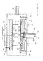
図1を参照して本発明に係るCVD装置の第1実施例を説明する。このCVD装置はB−W膜CVD装置であり、本装置では、反応容器11内の上方位置に反応ガス供給板12が設けられ、下方位置に基板保持体13が設けられる。基板保持体13は例えばアルミニウムで形成され、基板保持体13の上面に基板15が配置される。基板保持体13の平面形状は円形である。
【0032】
反応ガス供給板12の下面には所定位置に複数のガス吹出し孔12aが形成され、ガス供給管14で供給された反応ガスがガス吹出し孔12aから吹出し、反応容器11内に導入される。反応ガス供給板12の下面は、基板保持体13の上に配置された基板15に対向している。反応ガス供給板12の下面には同心円状に配置された径の小さい第1の円筒20と、径の大きい第2の円筒21が設けられる。円筒20,21の下端は基板15の処理面の付近まで延設される。円筒20,21の軸方向の長さは図示例ではほぼ同じであるが、異ならせることも可能である。上記のガス吹出し孔12aは、図1および図2に示すように、反応ガス供給板12の下面において円筒20の内部の下面領域、および円筒20と円筒21の間の下面領域に設けられる。円筒20内における反応ガス供給板12の下面領域では全領域にガス吹出し孔12aが形成され、円筒20と円筒21の間における反応ガス供給板12の下面領域では円筒21の内周縁に沿った円環状領域にガス吹出し孔12aが形成される。反応ガス供給板12で供給された反応ガスによって、基板15の表面に所望の薄膜が形成される。反応容器11内で生じた未反応ガスおよび副生成ガスは排気部16によって排気される。
【0033】
なお上記の孔12aは、直径が例えば0.5mm程度であり、例えば5mm程度のピッチで複数形成されている。
【0034】
基板保持体13の中心部には上下方向に貫通状態で形成された孔17が設けられ、この孔17は下方の差圧チャック排気部18と連結される。差圧チャック排気部18は、反応容器11に付設された上記排気部16とは別のものである。基板保持体13の上面には、基板15と接する部分に上記貫通孔17と連結された差圧溝19が設けられている。差圧溝19は、径方向に向かう放射状の例えば8本の直線溝(図示せず)と、同心円状に配置された例えば2本の円周溝とからなる。差圧溝19の深さは例えば1mm、幅は例えば1.5mmである。基板15が基板保持体13の上面に載置された後に差圧溝19を差圧チャック排気部18によって真空に排気すると、基板15の表面と差圧溝19との間に圧力差が生じる。この圧力差によって、基板15は基板保持体13の上に固定される。この基板固定手段によれば、基板15の成膜が行われる面に機械的な接触が直接的に行われず、基板15の表面全面に成膜を行うことができる。通常、この固定方法は差圧チャックまたは真空チャックと呼ばれる。なお固定手段としては、静電チャック装置を用いることもできる。
【0035】
上記の差圧溝19の構造によって、基板15を基板保持体13に固定することができる。本実施例のCVD装置の構造によれば、基板15の上面すなわち成膜面に対して直接に接触するものが存在しないために基板15の表面の温度分布は、基板保持体13の温度分布が均一ならば、基板15と基板保持体13の接触状態のみによって決定される。それ故に、基板15が基板保持体13上に均一に固定されるならば、基板15は均一な温度分布を持つことになる。
【0036】
反応容器11の下壁11aには、内外二重の筒体22が取り付けられる。筒体22は基板保持体13を支持する働きを有する。筒体22の下部は閉じられ、上部には連結体23が固設される。筒体22の内側筒部22aは上記孔17に通じる孔を形成し、筒体22の下壁から外部に延設される。筒体22の外側筒部22bと内側筒部22aの間の空間にはパージガス導入部24を介してパージガス(第1のパージガス)が供給される。上記連結体23には、その中央部に上記の孔17や内側筒部22a内の孔に通じる孔23aが形成され、その周囲部に例えば10本のパージガス供給路25が形成される。
【0037】
上記基板保持体13は、連結体23にネジ26で固定され、上記筒体22に取り付けられる。これによって基板保持体13は、筒体22に支持された状態で、反応容器11の下側中央部に好ましくはほぼ水平状態で配置される。基板保持体13と連結体23と支持用筒体22は一体的に形成される。この構造によって、差圧チャックを形成する孔17等、バージガス供給路25、反応容器11の内部空間が互いに隔離される。なお、連結体23と基板保持体13との接触面には、パージガスが通路外に漏れるのを防止するためのシール材27が設けられる。
【0038】
基板保持体13には、その表面に円形溝であるパージガス吹出し溝28が形成され、さらにその内部に例えば10本のパージガス通路29が形成される。10本のパージガス通路29の各々は、連結体23における対応するパージガス供給路25と、基板保持体13の上面に形成されたパージガス吹出し溝28とを接続する。各パージガス通路29は、パージガス導入部24によって導入される第1のパージガスをパージガス吹出し溝28に対して供給する。各パージガス通路29は、好ましくは水平であって基板保持体13の径方向を向いた径方向部と、好ましくは垂直であって基板保持体13の軸方向を向いた軸方向部とによって形成される。各パージガス通路29の径方向部は、等角度の間隔で放射状の位置に配置される。パージガス通路29の径方向部は、図1中下側に位置して円形のパージガス吹出し溝28の外壁面の半径よりも大きな長さを有する第1の径方向部と、図1中上側に位置してパージガス吹出し溝28の外壁面にパージガス吐出口(出口部)が形成される第2の径方向部とがある。パージガス通路29の形状は全体としてパージガス吹出し溝28の半径よりも長くなるように径方向に延設され、かつその後に垂直な軸方向部を経由して基板保持体13の中心部方向に折り返され、パージガス吹出し溝28に対してその外側から接続される。
【0039】
基板保持体13内に形成されるパージガス通路29は、実際には、それを形成する径方向部と軸方向部のそれぞれを個別に、基板保持体13の外表面から孔を開け、それぞれを接続することによって作製される。径方向部と軸方向部の各孔を作製した後に、当該孔の開口部は栓を埋めることにより閉じられる。
【0040】
また基板保持体13の上面では、バージガス吹出し溝28の内側に位置する表面すなわち基板配置面と、バージガス吹出し溝28の外側に位置する表面との間に段差が設けられる。この段差は、例えば0.2mmである。この段差が設けられることによって、基板15を基板配置面に配置したとき、基板15と基板保持体13の間にパージガスを吹出すための隙間30が形成される。
【0041】
また反応容器11の外面には、反応容器11を冷却するための複数の水冷通路31が設けられる。さらに基板保持体13の周囲にシールド部材32が配置される。このシールド部材32は、基板保持体13の側部周囲に位置する円筒部32aと、基板保持体13の上面の基板周囲の面を被うリング板部32bとからなる。シールド部材32の円筒部32aは、反応容器11の下壁11aに固定される。リング板部32bと基板保持体13との間の隙間は、室温では1mm程度の隙間として形成される。しかし、成膜温度のときには基板保持体13が熱膨脹し、当該隙間は0.2mm程度になり、基板15と基板保持体13の間に形成される上記隙間30とほぼ等しい隙間となる。従ってリング板部32bの内周縁と基板15の外周縁はほぼ同じ高さの位置に存在し、かつそれらの間に例えば1mm程度の隙間33が形成される。シールド部材32と基板保持体13とによって、パージガス導入部134で導入される第2のパージガスを流す供給路が形成される。
【0042】
第2のパージガスは、主に基板保持体13への成膜を防ぐためのものであり、リング板部32bを設け、このリング板部32bと基板保持体13との間に形成される隙間、およびリング板部32bの内周縁と基板15の外周縁との間の隙間33を通して第2のパージガスを吹出すようにしている。
【0043】
上記第2のパージガスは、基板保持体13のパージガス通路29およびパージガス吹出し溝28を通して供給される第1のパージガスと、隙間33付近で合流し、反応容器11の内部に吹出る。この場合において、隙間33の形成位置、第1および第2のパージガスの吹出し方向および合流作用によって、第2のパージガスは基板保持体13の表面または基板15に対してほぼ直角に吹出すことになる。第2のパージガスの吹出し作用によって、反応ガスが、基板保持体13とリング板部32bの間の隙間に侵入するのを防止することができる。さらに詳しくは、上方から隙間33付近への反応ガスは、合流したパージガスによって濃度が薄められ、基板15の裏面への反応ガスの侵入は隙間30から吹出る第1のパージガスによって防止され、基板保持体13とリング板部32bの間の隙間への反応ガスの侵入は第2のパージガスによって防止される。
【0044】
基板保持体13は、基板15を支持すると共に伝導作用によって基板15に必要な熱を与える。基板保持体13は、基板保持体13と反応容器11の下壁11aとの間に配置されたリング型平板状のセラミックヒータ34の輻射熱によって加熱される。セラミックヒータ34が配置される場所は、反応容器11内におけるパージガスが供給される通路の内部である。
【0045】
セラミックヒータ34は、少なくとも3つのセラミック製支持部35の上に、セラミック製ネジ36を用いて固定される。セラミックヒータ34の上面にはカーボンコーティング部37が設けられる。カーボンコーティング部37に、外部からの通電線38および配線固定ネジ39を経由して電流を供給することにより発熱作用を生じる。通電線38はシール部40を介して配線される。セラミックヒータ34と基板保持体13が近接して配置されるため、加熱効率が非常に良好となる。セラミックヒータ34の下側にはタンタル(Ta)等で形成された反射板41が配置される。
【0046】
基板保持体13の温度は、内部に埋め込まれた熱電対42によって測定され、その測定データは、その後、図示しない加熱制御系によって基板保持体13の温度制御に使用される。
【0047】
上記第1の円筒20の寸法は例えば外径28mm、長さ36mm、厚さ1.5mmであり、第2の円筒21の寸法は例えば外径150mm、長さ36mm、厚さ2mmである。また各円筒20,21の下端と基板15の表面との間隔はできるだけ小さいことが望ましいが、好ましくは例えば15mmである。当該間隔は、基板を基板保持体13の上に配置する搬送系のアームを入れるため最小限必要な間隔である。上記寸法を有する円筒20,21に関し、円筒20と円筒21の間における反応ガス供給板12の下面領域に形成されるガス吹出し孔12aが形成される領域は、反応ガス供給板12の中心から60〜75mmの距離を有する、円筒21の内周縁に沿った円環状領域である。反応ガス供給板12の基板対向面において上記のような形状の円筒20,21を設け、かつ円筒20,21の内部の所定の位置から反応ガスが供給されるようにガス吹出し孔12aを設けることによって、反応ガス供給板12から出た反応ガスを基板15の近くに集中させて導入できるようにしたため、これによって反応ガスの利用効率を向上することができる。なお円筒20,21については円筒の代わりに、同一の位置関係にある円形以外の他の形状の2つの筒体を用いることが可能である。
【0048】
成膜は、セラミックヒータ34で所定温度に保持された基板保持体13上に直径が例えば150mmの基板15を差圧チャックによって固定した後、反応ガス供給板12より反応ガスを導入して行われる。未反応ガスおよび副生成ガスは排気部16より排気される。また成膜時に基板15の裏面や基板保持体13等の成膜を行わないように、第1および第2のパージガスを導入する。
【0049】
上記実施例によるCVD装置の通常の成膜条件は、例えば、基板初期核形成の段階として、反応ガスWF6は2〜10sccm、SiH4は2〜10sccm、パージガス(Ar)が100〜500sccm、基板保持体13の温度は400〜500℃、圧力は0.5〜10Torrであり、H2還元により厚膜が形成される段階として、反応ガスWF6は50〜200sccm、H2は500〜2000sccm、パージガスは300〜1000sccm、基板保持体13の温度は400〜500℃、圧力は30〜70Torrである。
【0050】
本実施例では、特に、WF6が50sccm、H2が1000sccm、基板保持体温度が440℃、圧力が40Torrの条件で成膜を行い、成膜速度が0.5μm/分、基板面内分布(測定領域140mmφ)の標準偏差が±2.7%という良好な結果を得ることができた。
【0051】
一方、従来の同様なCVD装置では、WF6が100sccm、H2が1000sccm、基板保持体温度が440℃、圧力が40Torrの条件で成膜を行うと、基板面内分布(測定領域140mmφ)の標準偏差が±9%という結果が得られた。
【0052】
本実施例によるCVD装置では反応ガス利用効率は42%となり、従来装置の反応ガス利用効率13%に比較すると、大幅に改善することができた。
【0053】
上記第1実施例の変形例として、第1実施例の上記構成に加え、図5に示すように基板保持体13を上下に移動できるようにした移動機構(可動機構)を設けることもできる。この移動機構では、反応容器11の下壁11aに形成された孔に筒体22を密閉シールリング81を介して回転自在および軸方向に移動自在に設けると共に、その外面に雄ネジ部82を形成し、一方、反応容器11の下壁11aの外側に雌ネジ部83を備えた支持部材84が取り付けられる。筒体22の雄ネジ部82と支持部材84の雌ネジ部83とはネジ結合された状態にある。また筒体22の下部に設けられたギヤ85は、モータ86の出力軸に設けられたギヤ87と噛み合った状態に設けられる。なお図5中、セラミックヒータ等の図示は省略されている。かかる移動機構において、モータ86を回転駆動すると、上記のネジ結合部によって筒体22が回転しながら上下動し、こうして基板保持体13の上下動が行われる。かかる移動機構によって基板15の表面と円筒20,21の先端との間隔を例えば1mmとし、上記と同様な成膜を行った。この結果、成膜速度が0.7μm/分、基板面内分布(測定領域140mmφ)の標準偏差が±2.5%という良好な結果が得られた。また反応ガス利用効率は60%であった。
【0054】
なお上記実施例ではB−W膜CVD装置の例を説明したが、他のCVD装置、例えば、TiN、Cu、Al等のCVD装置にも適用できる。
【0055】
また上記実施例の他の効果として、基板保持体13の側から供給されるパージガスが基板15の表面に達するのを外側の円筒21で抑制することによって、基板周辺での成膜レート低下を押えることができ、これにより良好な基板面内分布を得ることができる。
【0056】
次に図3を参照して本発明に係るCVD装置の第2実施例について説明する。この実施例では、平行平板型のTi膜プラズマCVD装置を示す。図3において、図1に示した要素と実質的に同一の要素には同一の符号を付し、詳細な説明は省略する。以下、第1実施例の装置と相違する第2実施例の特徴的な構成、作用、効果を説明する。
【0057】
反応ガス供給板12には、反応容器11の上壁に設けられた電流導入端子51を経由して挿入される通電線52が接続される。通電線52の外側の端部は高周波電源に接続される。通電線52は、反応ガス供給板12と基板15との間に高い密度のプラズマを生成するための高周波電流を供給する。
【0058】
反応容器11の上壁の外側には、例えば外径が155mmで内径が135mmの円環状の磁石53と、例えば外径が20mmの円筒状磁石54が設けられる。磁石53の下面はN極、磁石54の下面はS極となっている。また反応容器11の下壁には、例えば外径155mm、内径145mmの円環状で上面がS極の磁石55が設けられる。これらの磁石53,54,55における対向するまたは近接する磁極部によって生成される磁束(磁力線)は、前述のプラズマ中を通り、プラズマ密度を高めるように形成される。かかる構成によって、プラズマ中の電子が、生成された磁力線に沿って螺旋運動を行うために、磁場がなく電子が直進する場合に比較して、電子の走行距離が長くなり、プラズマ中の電子と衝突する頻度が増すので、反応ガス供給板12と基板15との間のプラズマの密度がいっそう高くなり、基板15の表面での成膜速度が向上する。
【0059】
また第2実施例のCVD装置では、基板保持体13に載置される基板15を固定するための手段として静電チャックが使用される。従って、第1実施例のごとく基板保持体13に貫通孔17は形成されず、差圧チャック排気部18は設けられない。基板保持体13を支持するための筒体56は、二重構造ではない単純な筒体であり、第1のパージガスを導入するためのパージガス導入部24が設けられる。さらに基板保持体13の周囲に配置されるシールド部材57は、反応容器11の下壁に絶縁体58を介して設けられ、その周囲にさらにリング部材59が設けられる。
【0060】
また基板保持体13およびシールド部材57には、反応容器11の下壁に設けられた電流導入端子62を経由して挿入される通電線61が接続される。通電線61の外側端子は高周波電源に接続される。通電線61は、基板15およびシールド部材57にバイアスを加えるためのものである。通電線52によって反応ガス供給板12に高周波電流を供給し、通電線61によって基板15とシールド部材57にバイアスを加えるという構成によって、反応ガス供給板12と基板15との間に高い密度のプラズマが生成される。
【0061】
上記のごとく反応ガス供給板12と基板保持体13等の各々に所要の電力を供給することによって高密度のプラズマを発生させることができ、さらに磁石53,54,55を所定位置に設けることによってプラズマの密度をいっそう高めることができる。
【0062】
なお図3中では基板保持体13を加熱するための加熱装置、および水冷通路の図示が省略される。その他の構成は、前述した第1実施例による装置の構成と同じである。加熱装置は基板保持体13の内部に設けることもできる。特に、反応ガス供給板12の下面に同心円状に配置された第1と第2の円筒20,21を設け、円筒20の内部、および円筒20と円筒21の間に反応ガス吹出し孔12aを設けるようにした構成は、第1実施例と同様に第2実施例の特徴でもある。
【0063】
成膜を行う工程は前述の第1実施例と基本的に同じである。上記第2実施例によるCVD装置の通常の成膜条件は、例えば反応ガスTiCl4は1〜50sccm、H2は20〜2000sccm、パージガス(Ar)が300〜1000sccm、基板保持体13の温度は400〜600℃、圧力は0.1〜10Torrである。また反応ガス供給板12に周波数60MHz、電力100〜600Wを供給する。周波数を60MHzと高くしたため、電子の振幅が小さくなり、反応容器の壁部に衝突して電子が消失することが少なくなり、この結果、電子が消失するまでにプラズマ中の原子と衝突する頻度が増し、プラズマ密度が高くなり、成膜速度が向上する。また基板保持体13には周波数13.56MHz、電力10〜200Wを供給する。反応ガス供給板12と基板保持体13への電力供給は逆に接続することも、あるいは片方に電力を供給せず、接地することも可能である。
【0064】
本実施例では、特に、TiCl4が2sccm、H2が60sccm、基板保持体温度が600℃、圧力が1Torr、反応ガス供給板12への高周波周波数60MHz、電力600W、基板保持体13は接地の条件で成膜を行い、成膜速度が10nm/分が得られた。
【0065】
一方、従来のTi膜CVD装置では、TiCl4が2sccm、H2が60sccm、基板保持体温度が600℃、圧力が1Torr、反応ガス供給板13への高周波周波数13.56MHz、電力600Wの条件で2時間成膜を行ったが、成膜を観測することができなかった。
【0066】
上記第2実施例においても、第1実施例と同様に、移動機構によって基板保持体を上下し、基板15の表面と円筒20,21の先端との間隔を変えるようにすることもできる。当該間隔を1mmとすることにより、成膜速度15nm/分を得ることができた。
【0067】
次に、図4を参照して本発明に係るTi膜CVD装置の第3実施例について説明する。この実施例によるCVD装置は、第2実施例によるCVD装置の構成を変形したもので誘導結合型のプラズマCVD装置である。図4において、図1または図3に示した要素と実質的に同一要素には同一の符号を付し、詳細な説明は省略する。
【0068】
本実施例によるCVD装置では、反応ガス供給板12と基板保持体13の間に生成されるプラズマを高密度にするため、第2の円筒21の周囲にコイル71を複数巻きで巻き付けるようにした。このコイル71は反応容器11の上壁に設けられた電流導入端子72,73を介して外部に引き出される。なお第2実施例に示したように、反応ガス供給板12に電流を与えるための構成部分は設けられない。その他の構成および作用は、第2実施例で説明したものと同じである。
【0069】
コイル71の巻き数は任意であって、一巻きであっても構わない。
【0070】
成膜の工程では、基本的に第2実施例で説明されたものと同じである。相違する点は、コイル71に、例えば、周波数13.56MHz、電力100〜600Wを供給する点である。
【0071】
本実施例では、特に、TiCl4が2sccm、H2が60sccm、基板保持体温度が600℃、圧力が0.5Torr、コイル71への高周波電力600W、基板保持体13は接地の条件で成膜を行い、成膜速度が10nm/分が得られた。
【0072】
一方、従来のTi膜CVD装置では、TiCl4が2sccm、H2が60sccm、基板保持体温度が600℃、圧力が0.5Torr、反応ガス供給板12の高周波周波数13.56MHz、電力600Wの条件で2時間成膜を行ったが、成膜を観測することができなかった。
【0073】
上記第3実施例においても、第1実施例と同様に、移動機構によって基板保持体を上下し、基板15の表面と円筒20,21の先端との間隔を変えるようにすることもできる。当該間隔を1mmとすることにより、成膜速度15nm/分を得ることができた。
【0074】
【発明の効果】
以上の説明で明らかなように本発明によれば、次の効果を奏する。
【0075】
反応ガス供給板と、これに対向して配置される基板を保持する基板保持体を備えたCVD装置において、反応ガス供給板の基板対向面に同心円状に配置された内外二重の筒体を設けるようにし、この2つの筒体の内部空間を利用して反応ガスを誘導し、基板に対して導入するようにしたため、反応ガスを効率よく利用することができ、反応ガスの利用効率が高いCVD成膜を行うことができ、CVD装置において高い生産性と高い歩留まりを達成することができる。
【0076】
筒体と基板との間の間隔を変えるための構成を設けるようにしたため、最適な間隔を設定することができ、反応ガスの利用効率をCVD装置ごとに対応して最適なものにすることができる。
【0077】
反応ガス供給板と基板保持体に所要の電力を供給することにより、高い密度のプラズマを生成することができ、高い生産性と高い歩留まりのCVD装置を実現することができる。さらに反応容器の上側部分および下側部分に所定形状の任意の個数の磁石を配置することにより反応容器内のプラズマ空間を通る磁力線を形成し、これによってプラズマ密度をさらに高めることができ、生産性と歩留まりを高めることができる。
【0078】
また反応ガス供給板と基板対向面に設けられた外側筒体の周囲にコイルを設け、これに高周波電流を流すことにより生成されるプラズマの密度をさらに高めることができる。また基板保持体に所要の電力を供給する構造、あるいは反応容器の上側部分および下側部分に所定形状の任意の個数の磁石を配置する構造と組み合わせることにより、プラズマ密度をいっそう高めることができ、高い生産性と高い歩留まりのCVD装置を実現できる。
【図面の簡単な説明】
【図1】本発明に係るCVD装置の第1実施例を説明するための縦断面図である。
【図2】図1中の反応ガス供給板の下面図である。
【図3】本発明に係るCVD装置の第2実施例を説明するための縦断面図である。
【図4】本発明に係るCVD装置の第3実施例を説明するための縦断面図である。
【図5】筒体を上下動させる移動機構の一例を示す一部断面側面図である。
【符号の説明】
11 反応容器
12 反応ガス供給板
13 基板保持体
15 基板
20,21 円筒
12a ガス吹出し孔
53,54,55 磁石
71 コイル[0001]
[Industrial applications]
The present invention relates to a CVD apparatus used in a semiconductor device manufacturing process and for forming a thin film using vapor phase growth based on a chemical reaction.
[0002]
[Prior art]
In the field of recent semiconductor device manufacturing, integration and miniaturization of elements have been increasingly advanced. The miniaturization of elements requires a new technology in the manufacturing process. For example, there are demands for techniques for burying a sufficient film in a fine hole, reducing a step in an element, and preventing disconnection due to heat generation and electromigration caused by high current density. As a new manufacturing process that meets such demands, a CVD method (chemical method) is used instead of a sputtering method in forming a film such as Ti or TiN which is a base film of a wiring material such as aluminum (Al), tungsten (W), and copper (Cu). Vapor phase epitaxy) is attracting attention. For tungsten, especially WF6 (Tungsten hexaboride) gas and H2 Attention has been paid to the formation of a blanket tungsten film (hereinafter, referred to as a BW film) by a thermal CVD method using a gas.
[0003]
If the above-mentioned CVD method is used, sufficient step coverage can be obtained even in a hole having a hole diameter of 0.5 μm or less and an aspect ratio of 2 or more, and it is possible to meet the requirements for flattening and preventing electromigration in the device. it can.
[0004]
A conventional basic configuration of a BW film CVD apparatus will be outlined.
[0005]
A reaction gas supply plate for supplying a reaction gas is provided at an upper position in the reaction vessel, and a substrate holder for mounting a substrate is provided at a lower position. A desired thin film is formed on the substrate surface by the reaction gas supplied via the reaction gas supply plate. The substrate holder is heated by a heater. That is, it is a thermal CVD apparatus. The temperature of the substrate holder is measured by a thermocouple embedded therein, and the measured data is used for subsequent temperature control.
[0006]
A hole connected to the differential pressure chuck exhaust unit is provided at the center of the substrate holder, and a differential pressure groove communicating with the hole is formed on the substrate placement surface of the substrate holder. After the substrate is placed on the placement surface, the holes and the differential pressure grooves are evacuated by the differential pressure chuck exhaust unit, and the substrate is fixed on the substrate holder by the pressure difference generated between the front and back of the substrate. The substrate can be fixed by an electrostatic chuck instead of the differential pressure chuck.
[0007]
Further, a supply path for supplying a purge gas such as Ar is formed by utilizing a space provided inside or around the substrate holder, and the reaction is performed by blowing the purge gas from a gap provided below or around the substrate. Gas intrusion is prevented, and film formation on the back surface of the substrate and the substrate holder is prevented.
[0008]
The normal film forming conditions for the film formation in the BW film CVD apparatus are, for example, a reaction gas WF as a nucleation stage at the initial stage of film formation.6 Is 2-10 sccm, SiH4 Is formed at 2 to 10 sccm, the purge gas Ar is 100 to 500 sccm, the temperature of the substrate holder is 400 to 500 ° C., and the pressure is 0.5 to 10 Torr.2 The conditions under which the thick film is formed by the reduction of6 Is 100-200sccm, H2 Is 1000 to 2000 sccm, the purge gas Ar is 300 to 1000 sccm, the temperature of the substrate holder is 400 to 500 ° C., and the pressure is 30 to 70 Torr.
[0009]
The conventional structure of a Ti film CVD apparatus as another example of the CVD apparatus is basically the same as the above-described BW film CVD apparatus, and a reaction gas supply plate, a substrate holder, a purge gas A supply path, a heater for heating the substrate holder, a differential pressure chuck mechanism, an electrostatic chuck mechanism, and the like are provided. The difference between the Ti film CVD apparatus and the BW film CVD apparatus is that high frequency power is applied to the reaction gas supply plate from the current introduction terminal, thereby generating plasma between the reaction gas supply plate and the substrate holder. This is the point that is configured. That is, it is a parallel plate type plasma CVD apparatus.
[0010]
Typical film forming conditions for film formation in such a Ti film CVD apparatus include, for example, a reaction gas TiCl4 Is 1 to 50 sccm, H2 Is 20 to 2000 sccm, the purge gas Ar is 300 to 1000 sccm, the temperature of the substrate holder is 400 to 600 ° C., the pressure is 0.1 to 10 Torr, and the high frequency power is 100 to 600 W.
[0011]
[Problems to be solved by the invention]
In the conventional BW film CVD apparatus described above, since the substrate holder is separated from the reaction gas supply plate, the proportion of the reaction gas exhausted without reaching the substrate in the reaction gas supplied into the reaction vessel is reduced. Many. For this reason, there has been a problem that the ratio of tungsten contained in the reaction gas to be formed on the substrate to form a film, that is, the reaction gas utilization efficiency is low.
[0012]
As one method for solving the above-mentioned problem, there is a method of narrowing the distance between the substrate holder and the reactive gas supply plate. According to this solution, the reaction gas supply plate is heated by the heat of the substrate holder, the temperature rises, and a film is formed on the reaction gas supply plate. The formation of a film on a portion other than the substrate causes the generation of particles and dust (dust), and raises a problem that the yield is reduced.
[0013]
As another method for solving the problem of low reaction gas utilization efficiency, there is a method of rotating a substrate and a substrate holder. However, in this case, a waiting time (20 seconds until 1000 rpm) is required to stabilize the flow of the surrounding reactant gas accompanying the rotation, which poses a problem that productivity is reduced.
[0014]
In addition, in the conventional Ti film CVD apparatus, in addition to the above-described problem, there is a problem that the plasma density tends to be low because the substrate holder is separated from the reaction gas supply plate. For this reason, the film forming speed becomes slow. In addition, since unreacted gas and by-products are more likely to remain in the film, the productivity is reduced and the yield is reduced.
[0015]
As a method for solving the above-mentioned problem of the conventional Ti film CVD apparatus, there is a method using a high-density plasma source such as ECR (Electron Electron Resonance). However, there is a problem that the apparatus becomes large.
[0016]
A first object of the present invention is to solve the above problems, and an object of the present invention is to provide a CVD apparatus capable of forming a film with high reaction gas utilization efficiency and having high productivity and a high yield.
[0017]
A second object of the present invention is to provide a CVD apparatus having high productivity and high yield without increasing the size of the apparatus.
[0018]
[Means for Solving the Problems]
In order to achieve the above object, a CVD apparatus according to a first aspect of the present invention provides a reaction container, a substrate holder provided in the reaction container, a heating device for heating the substrate holder, and a substrate. A reaction gas supply plate for supplying a reaction gas to the inside of the reaction vessel, which is disposed to face the holder, and a device for forming a thin film on the surface of the substrate disposed on the substrate holder. At least two cylinders provided concentrically on the substrate facing surface are provided, for example, and the reaction gas is supplied from a portion of the reaction gas supply plate located inside each cylinder.
[0019]
A second aspect of the present invention (claim 2) is the CVD apparatus according to the first aspect, wherein a power supply device for supplying power to the reaction gas supply plate and the substrate holder is provided.
[0020]
A third aspect of the present invention (claim 3) is the CVD apparatus according to the second aspect, wherein annular magnets are provided on the upper and lower sides of the reaction vessel, and the upper and lower magnets face each other. The magnetic pole portion is configured to generate magnetic force lines passing through the plasma space.
[0021]
A fourth aspect of the present invention (claim 4) is the CVD apparatus according to the third aspect, wherein another cylindrical magnet is provided at a position of the center of the upper annular magnet, and a reaction vessel for the upper annular magnet is provided. Between the side magnetic pole part and the reaction vessel side magnetic pole part of the cylindrical magnet.Pass through plasma space The magnetic field lines are configured to be generated.
[0022]
A fifth aspect of the present invention (claim 5) is the CVD apparatus according to the first aspect, wherein a coil disposed around the outer cylinder is provided, and high-frequency power is supplied to the coil.
[0023]
A sixth aspect of the present invention (claim 6) is the CVD apparatus according to the fifth aspect, wherein a power supply device for supplying power to the substrate holder is provided.
[0024]
A seventh aspect of the present invention (claim 7) is the CVD apparatus according to the fifth or sixth aspect, wherein annular magnets are provided on the upper and lower sides of the reaction vessel, and the upper and lower magnets face each other. The magnetic pole portion is configured to generate magnetic force lines passing through the plasma space.
[0025]
An eighth aspect of the present invention (claim 8) is the CVD apparatus according to the seventh aspect, wherein a cylindrical magnet is provided at a position of a center of the upper annular magnet, and a reaction vessel side magnetic pole portion of the upper annular magnet is provided. Between the cylindrical magnet and the magnetic pole on the reaction vessel sidePass through plasma space The magnetic field lines are configured to be generated.
[0026]
A ninth aspect of the present invention (claim 9) is the CVD apparatus according to the first to eighth aspects, wherein the distance between the substrate holder and the reactive gas supply plate is set.To Changelike And a movable device (moving mechanism) for moving the substrate holder.
[0027]
[Action]
According to the present invention, in a CVD apparatus, a reaction gas is introduced by utilizing the internal space of each of two concentrically provided cylinders on an opposing surface of a reaction gas supply plate arranged opposite to a substrate holder. To induce a reaction gas. Thereby, the reaction gas supplied into the reaction vessel is efficiently used.
[0028]
Further, in the present invention, a high-density plasma is generated between the reaction gas supply plate to which necessary power is supplied and the substrate holder. Furthermore, the magnetic field lines generated in the plasma region by the magnets arranged in the upper part and the lower part of the reaction vessel further increase the plasma density in the plasma space.
[0029]
Further, in the present invention, the density of the plasma in the plasma space is further increased by using a coil provided around the outer cylinder and supplied with a high-frequency current.
[0030]
【Example】
Hereinafter, embodiments of the present invention will be described with reference to the accompanying drawings.
[0031]
A first embodiment of the CVD apparatus according to the present invention will be described with reference to FIG. This CVD apparatus is a BW film CVD apparatus. In this apparatus, a reaction
[0032]
A plurality of
[0033]
The
[0034]
A
[0035]
The
[0036]
An inner / outer
[0037]
The
[0038]
The
[0039]
The
[0040]
On the upper surface of the
[0041]
A plurality of
[0042]
The second purge gas is mainly for preventing film formation on the
[0043]
The second purge gas merges with the first purge gas supplied through the
[0044]
The
[0045]
The
[0046]
The temperature of the
[0047]
The dimensions of the
[0048]
The film is formed by fixing a
[0049]
The above embodimentTo The general film forming conditions of the CVD apparatus are, for example, a reaction gas6 Is 2-10 sccm, SiHFour Is 2 to 10 sccm, the purge gas (Ar) is 100 to 500 sccm, the temperature of the
[0050]
In this embodiment, in particular, WF6 Is 50 sccm, H2 Is formed under the conditions of 1000 sccm, a substrate holder temperature of 440 ° C., and a pressure of 40 Torr, a film forming rate of 0.5 μm / min, and a standard deviation of the in-plane distribution (measuring area 140 mmφ) of ± 2.7%. Good result was obtained.
[0051]
On the other hand, in a conventional similar CVD apparatus, WF6 Is 100sccm, HTwo Is 1000 sccm, the temperature of the substrate holder is 440 ° C., and the pressure is 40 Torr., Basis The result was that the standard deviation of the in-plate distribution (measuring area 140 mmφ) was ± 9%.
[0052]
In the CVD apparatus according to this embodiment, the reaction gas utilization efficiency was 42%, which was significantly improved as compared with the reaction gas utilization efficiency of the conventional apparatus of 13%.
[0053]
As a modified example of the first embodiment, in addition to the above-described configuration of the first embodiment, a moving mechanism (movable mechanism) that can move the
[0054]
In the above embodiment, the example of the BW film CVD apparatus has been described. However, the present invention can be applied to another CVD apparatus, for example, a CVD apparatus of TiN, Cu, Al or the like.
[0055]
Further, as another effect of the above-described embodiment, by suppressing the purge gas supplied from the
[0056]
Next, a second embodiment of the CVD apparatus according to the present invention will be described with reference to FIG. In this embodiment, a parallel plate type Ti film plasma CVD apparatus is shown. 3, elements substantially the same as the elements shown in FIG. 1 are denoted by the same reference numerals, and detailed description thereof will be omitted. Hereinafter, the characteristic configuration, operation, and effects of the second embodiment, which is different from the device of the first embodiment, will be described.
[0057]
The reaction
[0058]
An
[0059]
Further, in the CVD apparatus of the second embodiment, an electrostatic chuck is used as a means for fixing the
[0060]
The
[0061]
As described above, high-density plasma can be generated by supplying required electric power to each of the reaction
[0062]
In FIG. 3, the illustration of a heating device for heating the
[0063]
The process of forming a film is basically the same as that of the first embodiment. Second EmbodimentTo The usual film forming conditions of the CVD apparatus are, for example, the reaction gas TiClFour Is 1 to 50 sccm, HTwo Is 20 to 2000 sccm, the purge gas (Ar) is 300 to 1000 sccm, the temperature of the
[0064]
In this embodiment, in particular, TiCl4 Is 2sccm, H2 Is 60 sccm, the substrate holder temperature is 600 ° C., the pressure is 1 Torr, the high frequency frequency to the reaction
[0065]
On the other hand, in a conventional Ti film CVD apparatus, TiCl4 Is 2sccm, H2 Was formed under the conditions of 60 sccm, a substrate holder temperature of 600 ° C., a pressure of 1 Torr, a high frequency frequency of 13.56 MHz on the reaction
[0066]
In the second embodiment as well, as in the first embodiment, the distance between the surface of the
[0067]
Next, a third embodiment of the Ti film CVD apparatus according to the present invention will be described with reference to FIG. The CVD apparatus according to this embodiment is an inductively coupled plasma CVD apparatus obtained by modifying the configuration of the CVD apparatus according to the second embodiment. 4, substantially the same elements as those shown in FIG. 1 or FIG. 3 are denoted by the same reference numerals, and detailed description thereof will be omitted.
[0068]
In the CVD apparatus according to the present embodiment, the
[0069]
The number of turns of the
[0070]
The steps of film formation are basically the same as those described in the second embodiment. The difference is that, for example, a frequency of 13.56 MHz and a power of 100 to 600 W are supplied to the
[0071]
In this embodiment, in particular, TiCl4 Is 2sccm, H2 Is 60 sccm, the substrate holder temperature is 600 ° C., the pressure is 0.5 Torr, the high frequency power to the
[0072]
On the other hand, in a conventional Ti film CVD apparatus, TiCl4 Is 2sccm, H2 Was formed under the conditions of 60 sccm, a substrate holder temperature of 600 ° C., a pressure of 0.5 Torr, a high-frequency frequency of 13.56 MHz of the reactive
[0073]
In the third embodiment, similarly to the first embodiment, the distance between the surface of the
[0074]
【The invention's effect】
As apparent from the above description, the present invention has the following effects.
[0075]
In a CVD apparatus provided with a reaction gas supply plate and a substrate holder for holding a substrate arranged opposite thereto, an inner / outer double cylinder concentrically arranged on a substrate facing surface of the reaction gas supply plate is provided. Since the reaction gas is guided using the internal space of the two cylinders and introduced to the substrate, the reaction gas can be efficiently used, and the reaction gas utilization efficiency is high. A CVD film can be formed, and high productivity and high yield can be achieved in a CVD apparatus.
[0076]
Since the structure for changing the distance between the cylinder and the substrate is provided, the optimum distance can be set, and the utilization efficiency of the reaction gas can be optimized for each CVD apparatus. it can.
[0077]
By supplying required electric power to the reaction gas supply plate and the substrate holder, high-density plasma can be generated, and a CVD apparatus with high productivity and high yield can be realized. Further, by arranging an arbitrary number of magnets having a predetermined shape in the upper portion and the lower portion of the reaction vessel, magnetic lines of force passing through the plasma space in the reaction vessel are formed, thereby further increasing the plasma density, thereby improving productivity. And can increase the yield.
[0078]
In addition, a coil is provided around the reaction gas supply plate and the outer cylinder provided on the substrate facing surface, and the density of plasma generated by flowing a high-frequency current through the coil can be further increased. The plasma density can be further increased by combining with a structure for supplying required electric power to the substrate holder, or a structure in which an arbitrary number of magnets having a predetermined shape are arranged on the upper part and the lower part of the reaction vessel. A CVD apparatus with high productivity and high yield can be realized.
[Brief description of the drawings]
FIG. 1 shows a first embodiment of a CVD apparatus according to the present invention.Real It is a longitudinal section for explaining an example.
FIG. 2 is a bottom view of the reaction gas supply plate in FIG.
FIG. 3 is a longitudinal sectional view for explaining a second embodiment of the CVD apparatus according to the present invention.
FIG. 4 is a longitudinal sectional view for explaining a third embodiment of the CVD apparatus according to the present invention.
FIG. 5 is a partial cross-sectional side view illustrating an example of a moving mechanism that moves a cylinder up and down.
[Explanation of symbols]
11 Reaction vessel
12 reactive gas supply plate
13 Substrate holder
15 Substrate
20, 21 cylinder
12a Gas outlet
53,54,55 magnet
71 coil
Claims (9)
Translated fromJapanese前記反応ガス供給手段の基板対向面に同心状に設けられた少なくとも2つの筒体を備え、前記反応ガス供給手段における前記各筒体の内側に位置する部分から前記反応ガスを供給することを特徴とするCVD装置。A reaction vessel, a substrate holding means provided in the reaction vessel, a heating means for heating the substrate holding means, and a reaction gas arranged to face the substrate holding means and supplying a reaction gas into the reaction vessel A CVD apparatus for forming a thin film on a surface of a substrate arranged on the substrate holding means, comprising:
At least two cylinders are provided concentrically on the substrate facing surface of the reaction gas supply means, and the reaction gas is supplied from a portion of the reaction gas supply means located inside each of the cylinders. CVD apparatus.
Priority Applications (4)
| Application Number | Priority Date | Filing Date | Title |
|---|---|---|---|
| JP16695595AJP3599204B2 (en) | 1995-06-08 | 1995-06-08 | CVD equipment |
| TW085102914ATW293139B (en) | 1995-06-08 | 1996-03-11 | |
| US08/635,492US5676758A (en) | 1995-06-08 | 1996-04-22 | CVD apparatus |
| KR1019960014107AKR100208499B1 (en) | 1995-06-08 | 1996-05-01 | Cvd apparatus |
Applications Claiming Priority (1)
| Application Number | Priority Date | Filing Date | Title |
|---|---|---|---|
| JP16695595AJP3599204B2 (en) | 1995-06-08 | 1995-06-08 | CVD equipment |
Publications (2)
| Publication Number | Publication Date |
|---|---|
| JPH08337879A JPH08337879A (en) | 1996-12-24 |
| JP3599204B2true JP3599204B2 (en) | 2004-12-08 |
Family
ID=15840725
Family Applications (1)
| Application Number | Title | Priority Date | Filing Date |
|---|---|---|---|
| JP16695595AExpired - Fee RelatedJP3599204B2 (en) | 1995-06-08 | 1995-06-08 | CVD equipment |
Country Status (4)
| Country | Link |
|---|---|
| US (1) | US5676758A (en) |
| JP (1) | JP3599204B2 (en) |
| KR (1) | KR100208499B1 (en) |
| TW (1) | TW293139B (en) |
Families Citing this family (149)
| Publication number | Priority date | Publication date | Assignee | Title |
|---|---|---|---|---|
| JP3585606B2 (en)* | 1995-09-19 | 2004-11-04 | アネルバ株式会社 | Electrode device of CVD equipment |
| US6399143B1 (en) | 1996-04-09 | 2002-06-04 | Delsys Pharmaceutical Corporation | Method for clamping and electrostatically coating a substrate |
| US6499425B1 (en) | 1999-01-22 | 2002-12-31 | Micron Technology, Inc. | Quasi-remote plasma processing method and apparatus |
| US6123775A (en)* | 1999-06-30 | 2000-09-26 | Lam Research Corporation | Reaction chamber component having improved temperature uniformity |
| US6494955B1 (en) | 2000-02-15 | 2002-12-17 | Applied Materials, Inc. | Ceramic substrate support |
| US6502530B1 (en)* | 2000-04-26 | 2003-01-07 | Unaxis Balzers Aktiengesellschaft | Design of gas injection for the electrode in a capacitively coupled RF plasma reactor |
| US6503331B1 (en)* | 2000-09-12 | 2003-01-07 | Applied Materials, Inc. | Tungsten chamber with stationary heater |
| US6652713B2 (en)* | 2001-08-09 | 2003-11-25 | Applied Materials, Inc. | Pedestal with integral shield |
| US6730175B2 (en) | 2002-01-22 | 2004-05-04 | Applied Materials, Inc. | Ceramic substrate support |
| US7235139B2 (en)* | 2003-10-28 | 2007-06-26 | Veeco Instruments Inc. | Wafer carrier for growing GaN wafers |
| JP4590364B2 (en)* | 2005-03-16 | 2010-12-01 | 日本碍子株式会社 | Processing equipment |
| JP4405973B2 (en)* | 2006-01-17 | 2010-01-27 | キヤノンアネルバ株式会社 | Thin film production equipment |
| US20090277388A1 (en)* | 2008-05-09 | 2009-11-12 | Applied Materials, Inc. | Heater with detachable shaft |
| JP5445252B2 (en)* | 2010-03-16 | 2014-03-19 | 東京エレクトロン株式会社 | Deposition equipment |
| US9324576B2 (en) | 2010-05-27 | 2016-04-26 | Applied Materials, Inc. | Selective etch for silicon films |
| KR101671489B1 (en)* | 2010-07-29 | 2016-11-02 | 삼성디스플레이 주식회사 | Evaporation source for organic material and vapor depositing apparatus including the same |
| US10283321B2 (en) | 2011-01-18 | 2019-05-07 | Applied Materials, Inc. | Semiconductor processing system and methods using capacitively coupled plasma |
| US9064815B2 (en) | 2011-03-14 | 2015-06-23 | Applied Materials, Inc. | Methods for etch of metal and metal-oxide films |
| US8999856B2 (en) | 2011-03-14 | 2015-04-07 | Applied Materials, Inc. | Methods for etch of sin films |
| US8808563B2 (en) | 2011-10-07 | 2014-08-19 | Applied Materials, Inc. | Selective etch of silicon by way of metastable hydrogen termination |
| US9267739B2 (en) | 2012-07-18 | 2016-02-23 | Applied Materials, Inc. | Pedestal with multi-zone temperature control and multiple purge capabilities |
| US9373517B2 (en) | 2012-08-02 | 2016-06-21 | Applied Materials, Inc. | Semiconductor processing with DC assisted RF power for improved control |
| US9034770B2 (en) | 2012-09-17 | 2015-05-19 | Applied Materials, Inc. | Differential silicon oxide etch |
| US9023734B2 (en) | 2012-09-18 | 2015-05-05 | Applied Materials, Inc. | Radical-component oxide etch |
| US9390937B2 (en) | 2012-09-20 | 2016-07-12 | Applied Materials, Inc. | Silicon-carbon-nitride selective etch |
| US20140099794A1 (en)* | 2012-09-21 | 2014-04-10 | Applied Materials, Inc. | Radical chemistry modulation and control using multiple flow pathways |
| US9132436B2 (en) | 2012-09-21 | 2015-09-15 | Applied Materials, Inc. | Chemical control features in wafer process equipment |
| US8969212B2 (en) | 2012-11-20 | 2015-03-03 | Applied Materials, Inc. | Dry-etch selectivity |
| US8980763B2 (en) | 2012-11-30 | 2015-03-17 | Applied Materials, Inc. | Dry-etch for selective tungsten removal |
| US9111877B2 (en) | 2012-12-18 | 2015-08-18 | Applied Materials, Inc. | Non-local plasma oxide etch |
| US8921234B2 (en) | 2012-12-21 | 2014-12-30 | Applied Materials, Inc. | Selective titanium nitride etching |
| US10256079B2 (en) | 2013-02-08 | 2019-04-09 | Applied Materials, Inc. | Semiconductor processing systems having multiple plasma configurations |
| US9362130B2 (en) | 2013-03-01 | 2016-06-07 | Applied Materials, Inc. | Enhanced etching processes using remote plasma sources |
| US9040422B2 (en) | 2013-03-05 | 2015-05-26 | Applied Materials, Inc. | Selective titanium nitride removal |
| US20140271097A1 (en) | 2013-03-15 | 2014-09-18 | Applied Materials, Inc. | Processing systems and methods for halide scavenging |
| US9493879B2 (en) | 2013-07-12 | 2016-11-15 | Applied Materials, Inc. | Selective sputtering for pattern transfer |
| US9773648B2 (en) | 2013-08-30 | 2017-09-26 | Applied Materials, Inc. | Dual discharge modes operation for remote plasma |
| US9576809B2 (en) | 2013-11-04 | 2017-02-21 | Applied Materials, Inc. | Etch suppression with germanium |
| US9520303B2 (en) | 2013-11-12 | 2016-12-13 | Applied Materials, Inc. | Aluminum selective etch |
| US9245762B2 (en) | 2013-12-02 | 2016-01-26 | Applied Materials, Inc. | Procedure for etch rate consistency |
| US9287095B2 (en) | 2013-12-17 | 2016-03-15 | Applied Materials, Inc. | Semiconductor system assemblies and methods of operation |
| US9287134B2 (en) | 2014-01-17 | 2016-03-15 | Applied Materials, Inc. | Titanium oxide etch |
| US9293568B2 (en) | 2014-01-27 | 2016-03-22 | Applied Materials, Inc. | Method of fin patterning |
| US9396989B2 (en) | 2014-01-27 | 2016-07-19 | Applied Materials, Inc. | Air gaps between copper lines |
| US9385028B2 (en) | 2014-02-03 | 2016-07-05 | Applied Materials, Inc. | Air gap process |
| US9499898B2 (en) | 2014-03-03 | 2016-11-22 | Applied Materials, Inc. | Layered thin film heater and method of fabrication |
| US9299575B2 (en) | 2014-03-17 | 2016-03-29 | Applied Materials, Inc. | Gas-phase tungsten etch |
| US9299537B2 (en) | 2014-03-20 | 2016-03-29 | Applied Materials, Inc. | Radial waveguide systems and methods for post-match control of microwaves |
| US9299538B2 (en) | 2014-03-20 | 2016-03-29 | Applied Materials, Inc. | Radial waveguide systems and methods for post-match control of microwaves |
| US9903020B2 (en) | 2014-03-31 | 2018-02-27 | Applied Materials, Inc. | Generation of compact alumina passivation layers on aluminum plasma equipment components |
| US9269590B2 (en) | 2014-04-07 | 2016-02-23 | Applied Materials, Inc. | Spacer formation |
| JP6219229B2 (en)* | 2014-05-19 | 2017-10-25 | 東京エレクトロン株式会社 | Heater feeding mechanism |
| US9309598B2 (en) | 2014-05-28 | 2016-04-12 | Applied Materials, Inc. | Oxide and metal removal |
| US9378969B2 (en) | 2014-06-19 | 2016-06-28 | Applied Materials, Inc. | Low temperature gas-phase carbon removal |
| US9406523B2 (en) | 2014-06-19 | 2016-08-02 | Applied Materials, Inc. | Highly selective doped oxide removal method |
| US9425058B2 (en) | 2014-07-24 | 2016-08-23 | Applied Materials, Inc. | Simplified litho-etch-litho-etch process |
| US9378978B2 (en) | 2014-07-31 | 2016-06-28 | Applied Materials, Inc. | Integrated oxide recess and floating gate fin trimming |
| US9496167B2 (en) | 2014-07-31 | 2016-11-15 | Applied Materials, Inc. | Integrated bit-line airgap formation and gate stack post clean |
| US9659753B2 (en) | 2014-08-07 | 2017-05-23 | Applied Materials, Inc. | Grooved insulator to reduce leakage current |
| US9553102B2 (en) | 2014-08-19 | 2017-01-24 | Applied Materials, Inc. | Tungsten separation |
| US9355856B2 (en) | 2014-09-12 | 2016-05-31 | Applied Materials, Inc. | V trench dry etch |
| US9368364B2 (en) | 2014-09-24 | 2016-06-14 | Applied Materials, Inc. | Silicon etch process with tunable selectivity to SiO2 and other materials |
| US9355862B2 (en) | 2014-09-24 | 2016-05-31 | Applied Materials, Inc. | Fluorine-based hardmask removal |
| US9613822B2 (en) | 2014-09-25 | 2017-04-04 | Applied Materials, Inc. | Oxide etch selectivity enhancement |
| US9355922B2 (en) | 2014-10-14 | 2016-05-31 | Applied Materials, Inc. | Systems and methods for internal surface conditioning in plasma processing equipment |
| US9966240B2 (en) | 2014-10-14 | 2018-05-08 | Applied Materials, Inc. | Systems and methods for internal surface conditioning assessment in plasma processing equipment |
| US11637002B2 (en) | 2014-11-26 | 2023-04-25 | Applied Materials, Inc. | Methods and systems to enhance process uniformity |
| US9299583B1 (en) | 2014-12-05 | 2016-03-29 | Applied Materials, Inc. | Aluminum oxide selective etch |
| US10573496B2 (en) | 2014-12-09 | 2020-02-25 | Applied Materials, Inc. | Direct outlet toroidal plasma source |
| US10224210B2 (en) | 2014-12-09 | 2019-03-05 | Applied Materials, Inc. | Plasma processing system with direct outlet toroidal plasma source |
| US9502258B2 (en) | 2014-12-23 | 2016-11-22 | Applied Materials, Inc. | Anisotropic gap etch |
| US9343272B1 (en) | 2015-01-08 | 2016-05-17 | Applied Materials, Inc. | Self-aligned process |
| US11257693B2 (en) | 2015-01-09 | 2022-02-22 | Applied Materials, Inc. | Methods and systems to improve pedestal temperature control |
| US9373522B1 (en) | 2015-01-22 | 2016-06-21 | Applied Mateials, Inc. | Titanium nitride removal |
| US9449846B2 (en) | 2015-01-28 | 2016-09-20 | Applied Materials, Inc. | Vertical gate separation |
| US9728437B2 (en) | 2015-02-03 | 2017-08-08 | Applied Materials, Inc. | High temperature chuck for plasma processing systems |
| US20160225652A1 (en) | 2015-02-03 | 2016-08-04 | Applied Materials, Inc. | Low temperature chuck for plasma processing systems |
| US9881805B2 (en) | 2015-03-02 | 2018-01-30 | Applied Materials, Inc. | Silicon selective removal |
| US9741593B2 (en) | 2015-08-06 | 2017-08-22 | Applied Materials, Inc. | Thermal management systems and methods for wafer processing systems |
| US9691645B2 (en) | 2015-08-06 | 2017-06-27 | Applied Materials, Inc. | Bolted wafer chuck thermal management systems and methods for wafer processing systems |
| US9349605B1 (en) | 2015-08-07 | 2016-05-24 | Applied Materials, Inc. | Oxide etch selectivity systems and methods |
| US10504700B2 (en) | 2015-08-27 | 2019-12-10 | Applied Materials, Inc. | Plasma etching systems and methods with secondary plasma injection |
| US10522371B2 (en) | 2016-05-19 | 2019-12-31 | Applied Materials, Inc. | Systems and methods for improved semiconductor etching and component protection |
| US10504754B2 (en) | 2016-05-19 | 2019-12-10 | Applied Materials, Inc. | Systems and methods for improved semiconductor etching and component protection |
| US9865484B1 (en) | 2016-06-29 | 2018-01-09 | Applied Materials, Inc. | Selective etch using material modification and RF pulsing |
| US10629473B2 (en) | 2016-09-09 | 2020-04-21 | Applied Materials, Inc. | Footing removal for nitride spacer |
| US10062575B2 (en) | 2016-09-09 | 2018-08-28 | Applied Materials, Inc. | Poly directional etch by oxidation |
| US10546729B2 (en) | 2016-10-04 | 2020-01-28 | Applied Materials, Inc. | Dual-channel showerhead with improved profile |
| US10062585B2 (en) | 2016-10-04 | 2018-08-28 | Applied Materials, Inc. | Oxygen compatible plasma source |
| US9721789B1 (en) | 2016-10-04 | 2017-08-01 | Applied Materials, Inc. | Saving ion-damaged spacers |
| US9934942B1 (en) | 2016-10-04 | 2018-04-03 | Applied Materials, Inc. | Chamber with flow-through source |
| US10062579B2 (en) | 2016-10-07 | 2018-08-28 | Applied Materials, Inc. | Selective SiN lateral recess |
| US9947549B1 (en) | 2016-10-10 | 2018-04-17 | Applied Materials, Inc. | Cobalt-containing material removal |
| US10163696B2 (en) | 2016-11-11 | 2018-12-25 | Applied Materials, Inc. | Selective cobalt removal for bottom up gapfill |
| US9768034B1 (en) | 2016-11-11 | 2017-09-19 | Applied Materials, Inc. | Removal methods for high aspect ratio structures |
| US10026621B2 (en) | 2016-11-14 | 2018-07-17 | Applied Materials, Inc. | SiN spacer profile patterning |
| US10242908B2 (en) | 2016-11-14 | 2019-03-26 | Applied Materials, Inc. | Airgap formation with damage-free copper |
| US10566206B2 (en) | 2016-12-27 | 2020-02-18 | Applied Materials, Inc. | Systems and methods for anisotropic material breakthrough |
| US10431429B2 (en) | 2017-02-03 | 2019-10-01 | Applied Materials, Inc. | Systems and methods for radial and azimuthal control of plasma uniformity |
| US10403507B2 (en) | 2017-02-03 | 2019-09-03 | Applied Materials, Inc. | Shaped etch profile with oxidation |
| US10043684B1 (en) | 2017-02-06 | 2018-08-07 | Applied Materials, Inc. | Self-limiting atomic thermal etching systems and methods |
| US10319739B2 (en) | 2017-02-08 | 2019-06-11 | Applied Materials, Inc. | Accommodating imperfectly aligned memory holes |
| US10943834B2 (en) | 2017-03-13 | 2021-03-09 | Applied Materials, Inc. | Replacement contact process |
| US10319649B2 (en) | 2017-04-11 | 2019-06-11 | Applied Materials, Inc. | Optical emission spectroscopy (OES) for remote plasma monitoring |
| US11276559B2 (en) | 2017-05-17 | 2022-03-15 | Applied Materials, Inc. | Semiconductor processing chamber for multiple precursor flow |
| JP7176860B6 (en) | 2017-05-17 | 2022-12-16 | アプライド マテリアルズ インコーポレイテッド | Semiconductor processing chamber to improve precursor flow |
| US11276590B2 (en) | 2017-05-17 | 2022-03-15 | Applied Materials, Inc. | Multi-zone semiconductor substrate supports |
| US10049891B1 (en) | 2017-05-31 | 2018-08-14 | Applied Materials, Inc. | Selective in situ cobalt residue removal |
| US10497579B2 (en) | 2017-05-31 | 2019-12-03 | Applied Materials, Inc. | Water-free etching methods |
| US10920320B2 (en) | 2017-06-16 | 2021-02-16 | Applied Materials, Inc. | Plasma health determination in semiconductor substrate processing reactors |
| US11851763B2 (en)* | 2017-06-23 | 2023-12-26 | General Electric Company | Chemical vapor deposition during additive manufacturing |
| US10541246B2 (en) | 2017-06-26 | 2020-01-21 | Applied Materials, Inc. | 3D flash memory cells which discourage cross-cell electrical tunneling |
| US10727080B2 (en) | 2017-07-07 | 2020-07-28 | Applied Materials, Inc. | Tantalum-containing material removal |
| US10541184B2 (en) | 2017-07-11 | 2020-01-21 | Applied Materials, Inc. | Optical emission spectroscopic techniques for monitoring etching |
| US10354889B2 (en) | 2017-07-17 | 2019-07-16 | Applied Materials, Inc. | Non-halogen etching of silicon-containing materials |
| US10170336B1 (en) | 2017-08-04 | 2019-01-01 | Applied Materials, Inc. | Methods for anisotropic control of selective silicon removal |
| US10043674B1 (en) | 2017-08-04 | 2018-08-07 | Applied Materials, Inc. | Germanium etching systems and methods |
| US10297458B2 (en) | 2017-08-07 | 2019-05-21 | Applied Materials, Inc. | Process window widening using coated parts in plasma etch processes |
| US10128086B1 (en) | 2017-10-24 | 2018-11-13 | Applied Materials, Inc. | Silicon pretreatment for nitride removal |
| US10283324B1 (en) | 2017-10-24 | 2019-05-07 | Applied Materials, Inc. | Oxygen treatment for nitride etching |
| CN111417742B (en)* | 2017-11-28 | 2022-05-27 | 东京毅力科创株式会社 | Processing apparatus |
| US10256112B1 (en) | 2017-12-08 | 2019-04-09 | Applied Materials, Inc. | Selective tungsten removal |
| US10903054B2 (en) | 2017-12-19 | 2021-01-26 | Applied Materials, Inc. | Multi-zone gas distribution systems and methods |
| US11328909B2 (en) | 2017-12-22 | 2022-05-10 | Applied Materials, Inc. | Chamber conditioning and removal processes |
| US10854426B2 (en) | 2018-01-08 | 2020-12-01 | Applied Materials, Inc. | Metal recess for semiconductor structures |
| US10679870B2 (en) | 2018-02-15 | 2020-06-09 | Applied Materials, Inc. | Semiconductor processing chamber multistage mixing apparatus |
| US10964512B2 (en) | 2018-02-15 | 2021-03-30 | Applied Materials, Inc. | Semiconductor processing chamber multistage mixing apparatus and methods |
| TWI766433B (en) | 2018-02-28 | 2022-06-01 | 美商應用材料股份有限公司 | Systems and methods to form airgaps |
| US10593560B2 (en) | 2018-03-01 | 2020-03-17 | Applied Materials, Inc. | Magnetic induction plasma source for semiconductor processes and equipment |
| US10319600B1 (en) | 2018-03-12 | 2019-06-11 | Applied Materials, Inc. | Thermal silicon etch |
| US10497573B2 (en) | 2018-03-13 | 2019-12-03 | Applied Materials, Inc. | Selective atomic layer etching of semiconductor materials |
| US10526703B2 (en)* | 2018-03-15 | 2020-01-07 | Taiwan Semiconductor Manufacturing Company Ltd. | Film formation apparatus for forming semiconductor structure having shower head with plural hole patterns and with corresponding different plural hole densities |
| US10573527B2 (en) | 2018-04-06 | 2020-02-25 | Applied Materials, Inc. | Gas-phase selective etching systems and methods |
| US10490406B2 (en) | 2018-04-10 | 2019-11-26 | Appled Materials, Inc. | Systems and methods for material breakthrough |
| US10699879B2 (en) | 2018-04-17 | 2020-06-30 | Applied Materials, Inc. | Two piece electrode assembly with gap for plasma control |
| US10886137B2 (en) | 2018-04-30 | 2021-01-05 | Applied Materials, Inc. | Selective nitride removal |
| US10872778B2 (en) | 2018-07-06 | 2020-12-22 | Applied Materials, Inc. | Systems and methods utilizing solid-phase etchants |
| US10755941B2 (en) | 2018-07-06 | 2020-08-25 | Applied Materials, Inc. | Self-limiting selective etching systems and methods |
| US10672642B2 (en) | 2018-07-24 | 2020-06-02 | Applied Materials, Inc. | Systems and methods for pedestal configuration |
| US11049755B2 (en) | 2018-09-14 | 2021-06-29 | Applied Materials, Inc. | Semiconductor substrate supports with embedded RF shield |
| US10892198B2 (en) | 2018-09-14 | 2021-01-12 | Applied Materials, Inc. | Systems and methods for improved performance in semiconductor processing |
| US11062887B2 (en) | 2018-09-17 | 2021-07-13 | Applied Materials, Inc. | High temperature RF heater pedestals |
| US11417534B2 (en) | 2018-09-21 | 2022-08-16 | Applied Materials, Inc. | Selective material removal |
| US11682560B2 (en) | 2018-10-11 | 2023-06-20 | Applied Materials, Inc. | Systems and methods for hafnium-containing film removal |
| US11121002B2 (en) | 2018-10-24 | 2021-09-14 | Applied Materials, Inc. | Systems and methods for etching metals and metal derivatives |
| US11437242B2 (en) | 2018-11-27 | 2022-09-06 | Applied Materials, Inc. | Selective removal of silicon-containing materials |
| US11721527B2 (en) | 2019-01-07 | 2023-08-08 | Applied Materials, Inc. | Processing chamber mixing systems |
| US10920319B2 (en) | 2019-01-11 | 2021-02-16 | Applied Materials, Inc. | Ceramic showerheads with conductive electrodes |
| SG11202112556XA (en)* | 2019-05-15 | 2021-12-30 | Applied Materials Inc | Methods of reducing chamber residues |
Family Cites Families (3)
| Publication number | Priority date | Publication date | Assignee | Title |
|---|---|---|---|---|
| JPH0666298B2 (en)* | 1983-02-03 | 1994-08-24 | 日電アネルバ株式会社 | Dry etching equipment |
| US5230741A (en)* | 1990-07-16 | 1993-07-27 | Novellus Systems, Inc. | Gas-based backside protection during substrate processing |
| JPH04345022A (en)* | 1991-05-22 | 1992-12-01 | Sony Corp | Blanket metal cvd device |
- 1995
- 1995-06-08JPJP16695595Apatent/JP3599204B2/ennot_activeExpired - Fee Related
- 1996
- 1996-03-11TWTW085102914Apatent/TW293139B/zhnot_activeIP Right Cessation
- 1996-04-22USUS08/635,492patent/US5676758A/ennot_activeExpired - Lifetime
- 1996-05-01KRKR1019960014107Apatent/KR100208499B1/ennot_activeExpired - Fee Related
Also Published As
| Publication number | Publication date |
|---|---|
| TW293139B (en) | 1996-12-11 |
| JPH08337879A (en) | 1996-12-24 |
| KR100208499B1 (en) | 1999-07-15 |
| KR970001588A (en) | 1997-01-24 |
| US5676758A (en) | 1997-10-14 |
Similar Documents
| Publication | Publication Date | Title |
|---|---|---|
| JP3599204B2 (en) | CVD equipment | |
| US10062564B2 (en) | Method of selective gas phase film deposition on a substrate by modifying the surface using hydrogen plasma | |
| JP3555966B2 (en) | Multi-zone plasma processing method | |
| TWI877166B (en) | Substrate processing chamber | |
| US6364949B1 (en) | 300 mm CVD chamber design for metal-organic thin film deposition | |
| KR100445018B1 (en) | Method and Apparatus for Metallizing High Aspect Ratio Silicon Semiconductor Device Contacts | |
| TWI527116B (en) | Annular baffle | |
| US20020117399A1 (en) | Atomically thin highly resistive barrier layer in a copper via | |
| US7578946B2 (en) | Plasma processing system and plasma processing method | |
| EP0794553A2 (en) | High density plasma CVD and etching reactor | |
| US20110000619A1 (en) | Rotational antenna and semiconductor device including the same | |
| US6178920B1 (en) | Plasma reactor with internal inductive antenna capable of generating helicon wave | |
| JPH09237698A (en) | Inductive coupling plasma reactor, and method thereof | |
| JP7002655B2 (en) | Shape-selective deposition of dielectric film using low-frequency bias | |
| JP2003502824A (en) | Plasma reactor with multiple small internal induction antennas | |
| JP2002520492A (en) | Feedthrough overlapping coil | |
| US20030057845A1 (en) | Plasma processing apparatus | |
| WO2021132010A1 (en) | Film forming method and film forming system | |
| WO2006001253A1 (en) | Plasma processing equipment | |
| JP3720901B2 (en) | Plasma processing apparatus and antenna manufacturing method | |
| US20160379801A1 (en) | Rotational antenna and semiconductor device including the same | |
| JP3955351B2 (en) | Plasma processing equipment | |
| TWI894174B (en) | Method of depositing layers | |
| US10854432B2 (en) | Rotary plasma electrical feedthrough | |
| TW202124742A (en) | Method of depositing layers |
Legal Events
| Date | Code | Title | Description |
|---|---|---|---|
| A977 | Report on retrieval | Free format text:JAPANESE INTERMEDIATE CODE: A971007 Effective date:20040601 | |
| A131 | Notification of reasons for refusal | Free format text:JAPANESE INTERMEDIATE CODE: A131 Effective date:20040608 | |
| A521 | Request for written amendment filed | Free format text:JAPANESE INTERMEDIATE CODE: A523 Effective date:20040806 | |
| TRDD | Decision of grant or rejection written | ||
| A01 | Written decision to grant a patent or to grant a registration (utility model) | Free format text:JAPANESE INTERMEDIATE CODE: A01 Effective date:20040907 | |
| A61 | First payment of annual fees (during grant procedure) | Free format text:JAPANESE INTERMEDIATE CODE: A61 Effective date:20040909 | |
| R150 | Certificate of patent or registration of utility model | Free format text:JAPANESE INTERMEDIATE CODE: R150 | |
| FPAY | Renewal fee payment (event date is renewal date of database) | Free format text:PAYMENT UNTIL: 20070924 Year of fee payment:3 | |
| FPAY | Renewal fee payment (event date is renewal date of database) | Free format text:PAYMENT UNTIL: 20080924 Year of fee payment:4 | |
| FPAY | Renewal fee payment (event date is renewal date of database) | Free format text:PAYMENT UNTIL: 20080924 Year of fee payment:4 | |
| S531 | Written request for registration of change of domicile | Free format text:JAPANESE INTERMEDIATE CODE: R313531 | |
| S533 | Written request for registration of change of name | Free format text:JAPANESE INTERMEDIATE CODE: R313533 | |
| FPAY | Renewal fee payment (event date is renewal date of database) | Free format text:PAYMENT UNTIL: 20080924 Year of fee payment:4 | |
| R350 | Written notification of registration of transfer | Free format text:JAPANESE INTERMEDIATE CODE: R350 | |
| FPAY | Renewal fee payment (event date is renewal date of database) | Free format text:PAYMENT UNTIL: 20090924 Year of fee payment:5 | |
| FPAY | Renewal fee payment (event date is renewal date of database) | Free format text:PAYMENT UNTIL: 20090924 Year of fee payment:5 | |
| FPAY | Renewal fee payment (event date is renewal date of database) | Free format text:PAYMENT UNTIL: 20100924 Year of fee payment:6 | |
| FPAY | Renewal fee payment (event date is renewal date of database) | Free format text:PAYMENT UNTIL: 20100924 Year of fee payment:6 | |
| FPAY | Renewal fee payment (event date is renewal date of database) | Free format text:PAYMENT UNTIL: 20110924 Year of fee payment:7 | |
| FPAY | Renewal fee payment (event date is renewal date of database) | Free format text:PAYMENT UNTIL: 20110924 Year of fee payment:7 | |
| FPAY | Renewal fee payment (event date is renewal date of database) | Free format text:PAYMENT UNTIL: 20120924 Year of fee payment:8 | |
| FPAY | Renewal fee payment (event date is renewal date of database) | Free format text:PAYMENT UNTIL: 20120924 Year of fee payment:8 | |
| FPAY | Renewal fee payment (event date is renewal date of database) | Free format text:PAYMENT UNTIL: 20130924 Year of fee payment:9 | |
| LAPS | Cancellation because of no payment of annual fees |