JP3595504B2 - Computer processing method in multi-thread processor - Google Patents
Computer processing method in multi-thread processorDownload PDFInfo
- Publication number
- JP3595504B2 JP3595504B2JP2000517336AJP2000517336AJP3595504B2JP 3595504 B2JP3595504 B2JP 3595504B2JP 2000517336 AJP2000517336 AJP 2000517336AJP 2000517336 AJP2000517336 AJP 2000517336AJP 3595504 B2JP3595504 B2JP 3595504B2
- Authority
- JP
- Japan
- Prior art keywords
- thread
- switch
- processor
- execution
- cache
- Prior art date
- Legal status (The legal status is an assumption and is not a legal conclusion. Google has not performed a legal analysis and makes no representation as to the accuracy of the status listed.)
- Expired - Fee Related
Links
Images


Classifications
- G—PHYSICS
- G06—COMPUTING OR CALCULATING; COUNTING
- G06F—ELECTRIC DIGITAL DATA PROCESSING
- G06F9/00—Arrangements for program control, e.g. control units
- G06F9/06—Arrangements for program control, e.g. control units using stored programs, i.e. using an internal store of processing equipment to receive or retain programs
- G06F9/46—Multiprogramming arrangements
- G06F9/48—Program initiating; Program switching, e.g. by interrupt
- G06F9/4806—Task transfer initiation or dispatching
- G06F9/4843—Task transfer initiation or dispatching by program, e.g. task dispatcher, supervisor, operating system
- G—PHYSICS
- G06—COMPUTING OR CALCULATING; COUNTING
- G06F—ELECTRIC DIGITAL DATA PROCESSING
- G06F9/00—Arrangements for program control, e.g. control units
- G06F9/06—Arrangements for program control, e.g. control units using stored programs, i.e. using an internal store of processing equipment to receive or retain programs
- G06F9/30—Arrangements for executing machine instructions, e.g. instruction decode
- G06F9/30003—Arrangements for executing specific machine instructions
- G06F9/30076—Arrangements for executing specific machine instructions to perform miscellaneous control operations, e.g. NOP
- G06F9/3009—Thread control instructions
- G—PHYSICS
- G06—COMPUTING OR CALCULATING; COUNTING
- G06F—ELECTRIC DIGITAL DATA PROCESSING
- G06F9/00—Arrangements for program control, e.g. control units
- G06F9/06—Arrangements for program control, e.g. control units using stored programs, i.e. using an internal store of processing equipment to receive or retain programs
- G06F9/30—Arrangements for executing machine instructions, e.g. instruction decode
- G06F9/38—Concurrent instruction execution, e.g. pipeline or look ahead
- G06F9/3836—Instruction issuing, e.g. dynamic instruction scheduling or out of order instruction execution
- G06F9/3851—Instruction issuing, e.g. dynamic instruction scheduling or out of order instruction execution from multiple instruction streams, e.g. multistreaming
Landscapes
- Engineering & Computer Science (AREA)
- Software Systems (AREA)
- Theoretical Computer Science (AREA)
- Physics & Mathematics (AREA)
- General Engineering & Computer Science (AREA)
- General Physics & Mathematics (AREA)
- Multimedia (AREA)
- Memory System Of A Hierarchy Structure (AREA)
- Advance Control (AREA)
- Executing Machine-Instructions (AREA)
Description
Translated fromJapanese【0001】
【発明の属する技術分野】
関連特許出願データ
本発明は、下記の米国特許出願に関連する:(1)米国特許出願第08/958716号明細書、(2)米国特許出願第08/956875号明細書、(3)米国特許出願第08/958718号明細書、(4)米国特許出願第08/956577号明細書、(5)米国特許出願第773572号明細書、(6)米国特許出願第761378号明細書、(7)米国特許出願第761380号明細書、(8)米国特許出願第761379号明細書、(9)米国特許出願第473692号明細書、(10)米国特許第5778243号明細書。
【0002】
【従来の技術】
本発明は、全般的にはコンピュータ・データ処理システムのための改良された方法およびその装置に関し、具体的には、改良された高性能マルチスレッド式コンピュータ・データ処理システムと、そのプロセッサのハードウェア内で実施される方法に関する。
【0003】
現代のコンピュータの基本構造には、外部の世界との間で情報を通信するための周辺装置が含まれ、そのような周辺装置は、キーボード、モニタ、テープ駆動装置、ネットワークに接続された通信回線などとすることができる。やはりコンピュータの基本構造に含まれるのが、外部の世界との間でこの情報を受け取り、処理し、配送するのに必要なハードウェアであり、これには、バス、メモリ・ユニット、入出力コントローラ、記憶装置、少なくとも1つの中央処理装置(CPU)などが含まれる。CPUは、システムの頭脳である。CPUは、コンピュータ・プログラムを含む命令を実行し、他のシステム構成要素の動作を指示する。
【0004】
コンピュータのハードウェアの観点から、ほとんどのシステムは、基本的に同一の形で動作する。プロセッサは、実際には、算術演算、論理比較、ある位置から別の位置へのデータの移動など、非常に単純な動作をすばやく実行する。これらの単純な動作を大量に実行するようにコンピュータに指示するプログラムが、コンピュータが洗練されたことを行っているという錯覚をもたらす。しかし、コンピュータの新機能または改良された機能としてユーザに知覚されるものは、実際には、同一の単純な動作をはるかに高速に実行する計算機である場合がある。したがって、コンピュータ・システムに対する改良を継続するためには、これらのシステムをさらに高速にする必要がある。
【0005】
コンピュータ・システムの総合速度の尺度の1つをスループットとも称するが、これは、単位時間あたりに実行される動作の数として測定される。概念上、システム速度に対するすべての可能な改良のうちで最も単純なものは、さまざまな構成要素のクロック速度、特にプロセッサのクロック速度を高めることである。したがって、すべてが2倍の速度で走行するが、それ以外は正確に同一の形で機能する場合、そのシステムは、所与のタスクを半分の時間で実行することになる。以前に別個の構成要素から構成されていたコンピュータ・プロセッサは、構成要素のサイズの縮小と個数の減少とによって大幅に高速に動作するようになり、最終的には、プロセッサ全体が、単一チップ上の集積回路としてパッケージされるようになった。サイズの縮小によって、プロセッサのクロック速度を高めることが可能になり、したがって、システム速度を高めることが可能になった。
【0006】
集積回路から得られる速度の大幅な向上にもかかわらず、さらに高速のコンピュータ・システムに対する需要がいまだに存在する。ハードウェア設計者は、より大規模の集積、回路のサイズのさらなる縮小および他の技法によって、さらなる速度の向上を得ることができた。しかし、設計者は、物理的なサイズの縮小を際限なく継続することは不可能であり、継続的にプロセッサ・クロック速度を高めることに限界があると考えている。したがって、コンピュータ・システムの総合速度をさらに改善するために、他の手法に注意が向けられた。
【0007】
クロック速度を変更しなくても、複数のプロセッサを使用することによってシステム速度を改善することが可能である。集積回路チップにパッケージされた個々のプロセッサのコストが適度であるので、これが実用的になった。スレーブ・プロセッサを使用すると、作業をCPUからスレーブ・プロセッサにオフロードすることによって、システム速度がかなり改善される。たとえば、スレーブ・プロセッサは、通常は、入出力装置の通信および制御など、反復的で単純な専用プログラムを実行する。複数のCPUを単一のコンピュータ・システム、通常は複数のユーザを同時にサービスするホストベース・システム内に配置することも可能である。異なるCPUのそれぞれが、異なるユーザのために異なるタスクを別々に実行することができ、したがって、複数のタスクを同時に実行するシステムの総合速度が高まる。しかし、アプリケーション・プログラムなどの単独のタスクが実行される速度を改善することは、はるかに困難である。複数のCPUの間でさまざまな機能の実行および結果の配布を調整することは、注意を要する作業である。スレーブ入出力プロセッサの場合、機能が事前に定義され、制限されているので、これはそれほど困難ではないが、汎用アプリケーション・プログラムを実行する複数のCPUの場合、システム設計者がプログラムの詳細を事前に知らないことが一因となって、機能を調整することがより困難になる。ほとんどのアプリケーション・プログラムは、プロセッサによって実行されるステップの単一の経路または流れに従う。この単一の経路を複数の並列経路に分割することが可能である場合もあるが、それを行うための万能のアプリケーションは、まだ研究中である。一般に、複数のプロセッサによる並列処理のために長いタスクを小さいタスクに分割することは、コードを記述するソフトウェア・エンジニアによって、ケースバイケースで行われる。この、その場限りの手法は、必ずしも反復的でなく、予測可能でもない商業トランザクションを実行する場合に特に問題がある。
【0008】
したがって、複数のプロセッサによって総合的なシステム性能は改善されるが、個々のCPUの速度を改善する理由はまだ多数存在する。CPUクロック速度が与えられた場合、1クロック・サイクルあたりに実行される命令の「平均」数を増やすことによって、CPUの速度すなわち1秒あたりに実行される命令の数をさらに増やすことが可能である。高性能単一チップ・マイクロプロセッサのための一般的なアーキテクチャが、高速実行のために頻繁に使用される命令の小さい簡略されたセットを特徴とする縮小命令セット・コンピュータ(RISC)アーキテクチャであり、これらの単純な動作は、前に述べたものより高速に実行される。半導体技術が進歩するにつれて、RISCアーキテクチャの目標は、計算機の各クロック・サイクルに1つまたは複数の命令を実行できるプロセッサの開発になってきた。1クロック・サイクルあたりに実行される命令の「平均」数を増やすためのもう1つの手法が、CPU内のハードウェアを変更することである。この命令あたりのクロック数というスループット尺度は、高性能プロセッサのアーキテクチャの特徴を表すのに一般的に使用されている。命令パイプライン化とキャッシュ・メモリが、これを達成することを可能にしたコンピュータ・アーキテクチャの特徴である。パイプライン命令実行を用いると、前に発行された命令が完了する前に、後続の命令の実行を開始できるようになる。キャッシュ・メモリは、頻繁に使用されるデータおよび他のデータをプロセッサの近くに格納し、これによって、ほとんどの場合に主記憶のフル・アクセス・タイムを待つことなしに、命令実行を継続できるようにするものである。並列に実行する命令を見つけるためのルック・アヘッド・ハードウェアを有する複数の実行ユニットを用いるいくつかの改良も示されてきた。
【0009】
通常のRISCプロセッサの性能は、スーパースカラ・コンピュータおよびVLIW(Very Long Instruction Word)コンピュータでさらに高めることができ、これらのコンピュータの両方が、1プロセッサ・サイクルあたりに複数の命令を並列に実行する。これらのアーキテクチャでは、複数の機能ユニットまたは実行ユニットを設けて、複数のパイプラインを並列に走行させる。スーパースカラ・アーキテクチャでは、命令は、インオーダー(in−order)またはアウトオブオーダー(out−of−order)で完了できる。インオーダー完了とは、ある命令の前にディスパッチされたすべての命令が完了するまでは、その命令を完了できないことを意味する。アウトオブオーダー完了とは、事前に定義された規則が満たされる限り、ある命令の前のすべての命令が完了する前に、その命令が完了することを許可されることを意味する。
【0010】
スーパースカラ・システムでの命令のインオーダー完了とアウトオブオーダー完了の両方について、パイプラインは、ある状況の下でストールする。前にディスパッチされ、まだ完了していない命令の結果に依存する命令が、パイプラインのストールを引き起こす可能性がある。たとえば、必要なデータがキャッシュ内にない、すなわち、キャッシュ・ミスを引き起こすロード/ストア命令に依存する命令は、そのデータがキャッシュ内で使用可能になるまでは実行できない。継続実行のため、また、高いヒット率すなわちデータがキャッシュ内ですぐに使用可能である回数と比較したデータに対する要求の回数を維持するために必要な、キャッシュ内の必要不可欠なデータを維持することは、特に大きいデータ構造を伴う計算の場合には簡単ではない。キャッシュ・ミスは、数サイクルにわたるパイプラインのストールを引き起こす可能性があり、データがほとんどの時間に使用可能でない場合には、メモリ待ち時間の総量が厳しくなる。主記憶に使用される記憶装置は、高速になりつつあるが、そのようなメモリ・チップとハイエンド・プロセッサの間の速度ギャップは、ますます大きくなりつつある。したがって、現在のハイエンド・プロセッサ設計での実行時間のかなりの量が、キャッシュ・ミスの解決を待つのに費やされ、これらのメモリ・アクセスの遅れが、プロセッサ実行時間のうちで占める比率がますます大きくなっている。
【0011】
CPU内のハードウェアの効率を改善するためのもう1つの技法が、処理タスクを、スレッドと称する独立に実行可能な命令のシーケンスに分割することである。この技法は、スレッドが同一のプロセッサによって実行される点を除いて、異なるプロセッサによる独立実行のために大きいタスクを小さいタスクに分割することに関連する。CPUが、複数の理由のいずれかのために、これらのスレッドのうちの1つの処理または実行を継続できない時には、CPUは、別のスレッドに切り替え、そのスレッドを実行する。コンピュータ・アーキテクチャ界で定義される用語「マルチスレッディング」は、複数の関連するスレッドに分割された1つのタスクを意味するソフトウェアでのこの用語の使用と同一ではない。アーキテクチャ的定義では、スレッドは、独立とすることができる。したがって、この2つの用語の使用を区別するために、「ハードウェア・マルチスレッディング」が使用されることがしばしばである。本発明の文脈では、用語「マルチスレッディング」は、メモリ待ち時間を許容するためのハードウェア・マルチスレッディングを含む。
【0012】
マルチスレッディングを用いると、プロセッサのパイプラインが、現在のスレッドに関してパイプライン・ストール状態が検出された時に、異なるスレッド上の有用な作業を行えるようになる。マルチスレッディングを用いると、非パイプライン・アーキテクチャを実施するプロセッサが、現在のスレッドに関してストール状態が検出された時に、別のスレッドに関して有用な作業を行えるようにもなる。マルチスレッディングには、2つの基本形態がある。従来の形態では、プロセッサ内でN個のスレッドまたは状態を保ち、サイクル単位でスレッドをインターリーブする。これによって、単一のスレッド内の命令が分離されるので、すべてのパイプライン依存性が除去される。本発明によって考慮される、マルチスレッディングのもう1つの形態では、いくつかの長い待ち時間のイベントの際にスレッドをインターリーブする。
【0013】
マルチスレッディングの従来の形態では、スレッドごとのプロセッサ・レジスタの複製が用いられる。たとえば、商品名PowerPC(商標)の下で販売されるアーキテクチャを実施するプロセッサがマルチスレッディングを実行するためには、プロセッサは、N個のスレッドを走行させるためにN個の状態を維持しなければならない。したがって、汎用レジスタ、浮動小数点レジスタ、条件レジスタ、浮動小数点状態および制御レジスタ、カウント・レジスタ、リンク・レジスタ、例外レジスタ、セーブ/リストア・レジスタおよび特殊目的レジスタが、N回複製される。さらに、セグメント・ルックアサイド・バッファなどの特殊バッファを複製することができ、また、各項目にスレッド番号のタグを付けることができ、タグを付けない場合にはスレッド切り替えのたびにフラッシュしなければならない。また、一部の分岐予測機構、たとえば相関レジスタとリターン・スタックなども、複製しなければならない。幸い、レベル1命令キャッシュ(L1 I−キャッシュ)、レベル1データ・キャッシュ(L1 D−キャッシュ)、命令バッファ、ストア待ち行列、命令ディスパッチャ、機能ユニットまたは実行ユニット、パイプライン、変換ルックアサイド・バッファ(TLB)および分岐履歴テーブルなどのプロセッサのより大きい機能のうちのいくつかは、複製する必要がない。あるスレッドが遅延に遭遇した時に、プロセッサは、すばやく別のスレッドに切り替える。このスレッドの実行は、第1のスレッドでのメモリ遅延とオーバーラップする。
【0014】
既存のマルチスレッディング技法では、キャッシュ・ミスまたはメモリ参照の際のスレッド切り替えが説明される。この技法の主な例は、アガーワル(Agarwal)他著、「Sparcle: An Evolutionary Design for Large−Scale Multiprocessors」、IEEE Micro Volume 13、No.3、pp.48−60、1993年6月に記載されている。RISCアーキテクチャで適用される際には、通常は関数呼出しのサポートに使用される複数のレジスタ・セットが、複数のスレッドを維持するように変更される。8つのオーバーラップするレジスタ・ウィンドウが、4つのオーバーラップしないレジスタ・セットになるように変更され、各レジスタ・セットは、トラップおよびメッセージ処理のために予約される。このシステムでは、リモート・メモリ要求をもたらす第1レベルのキャッシュ・ミスのそれぞれで発生するスレッド切替えが開示される。このシステムは、当技術分野での進歩を表すが、現代のプロセッサ設計では、プロセッサに付加される複数のレベルのキャッシュ・メモリまたは高速メモリが使用されることがしばしばである。
【0015】
プロセッサ・システムは、周知のアルゴリズムを使用して、その主メモリ記憶域のどの部分がキャッシュの各レベルにロードされるかを決定し、したがって、第1レベルのキャッシュ内に存在しないメモリ参照が発生するたびに、プロセッサは、第2レベルまたはさらに上位のレベルのキャッシュからのそのメモリ参照の取得を試みなければならない。
【0016】
欧州特許EP 0 747 816 A2号明細書に、メモリ待ち時間に起因する遅延を減らす、改良された高性能マルチスレッド式データ処理システムが記載されている。このシステムでは、初期スレッド内の少なくとも1つの命令が実行される。その後、レベル2またはそれより上位のキャッシュ・ミスに応答してのみ、第1スレッド内の選択された点でのプロセッサの状態が記憶され、第1スレッドの実行が打ち切られ、実行のために第2スレッドが選択され、これによって、メモリ待ち時間に起因するプロセッサ遅延が最小になる。
【0017】
IEEE Micro誌、vol.17, no.5, 1997年9月、第12〜19ページに掲載の論文「Simultaneous Multithreading: A Platform for Next−Generation Processors」、(以下では「Eggers」論文と呼称する)に、同時マルチスレッディングが、同一サイクル内に異なるスレッドから命令を発行することによって、命令レベルとスレッド・レベルの両方の並列性を活用する方法に関する一般的な議論が記載されている。
【0018】
欧州特許EP 0 527 392 A2号明細書によれば、マルチタスキング・オペレーティング・システム内のアプリケーション・プログラムが、プログラム・スレッドのパラメータを指定することによって、プログラム・スレッドの実行のスケジュールに影響を及ぼすことが可能になる。このパラメータでは、各スレッドの優先順位レベルと、そのスレッドが常駐するディスパッチ・クラスが示される。オペレーティング・システムは、各ディスパッチ・クラスから実行のために使用可能な最高の優先順位のスレッドを、プロセッサによる実行のための走行リスト上に待ち行列化する。走行リスト上の最高の優先順位のスレッドが、最初に実行される。
【0019】
このスレッドは、ディスパッチ可能であり、実行中であるが、同一のディスパッチ・クラスからの他のスレッドは、他のスレッドがより高い優先順位を有する場合であっても、この実行中のスレッドが自発的にプロセッサの制御を放棄しない限り、そのスレッドに対する優先使用を行うことができない。
【0020】
【発明が解決しようとする課題】
したがって、本発明の目的は、マルチスレッド式データ処理システムで実施されるハードウェア論理およびレジスタを使用する、マルチレベル・キャッシュ・システムでのメモリ待ち時間に起因する遅延を減らすことのできる、改良されたデータ処理システムを提供することである。
【0021】
【課題を解決するための手段】
本発明は、命令の2つのスレッドの間で実行を切り替える能力を有するマルチスレッド式プロセッサと、任意選択のスレッド切替え条件のソフトウェア・オーバーライドを有するハードウェア・レジスタで実施されるスレッド切替え論理とを提供することによって、この目的に対処する。命令のさまざまなスレッドのさまざまな状態を処理することによって、スレッドの間でのプロセッサの使用を最適化できるようになる。プロセッサが命令の第2のスレッドを実行できるようにすることによって、(そうでなければ、キャッシュ、メモリ、外部入出力、直接アクセス記憶装置などのさまざまな記憶要素から第1スレッドのために必要なデータまたは命令を取り出している時に、遊休状態になる)プロセッサの利用度が高まる。スレッド切替えの条件は、スレッドごとに異なるものとすることができ、また、ソフトウェア・スレッド制御マネージャの使用によって処理中に変更することができる。
【0022】
第1スレッドが、キャッシュ・ミスなどの完了に多数のサイクルを必要とする待ち時間イベントを有する時に、第2スレッドを処理することができるが、この待ち時間イベント中に、第2スレッドも、同一のキャッシュ・レベルまたは異なるキャッシュ・レベルで、ただしはるかに短い時間で完了できるキャッシュ・ミスを、経験する可能性がある。
【0023】
命令実行なしでスレッドを切り替えるサイクルの反復で各スレッドがロックするスラッシングは、本発明によって、プログレス・カウント・レジスタを実施し、プログラム可能な最大回数までのスレッド切替えを許容し、それを超えた時点であるスレッドが実行可能になるまでプロセッサがスレッドの切替えを停止するようにする方法を実施することによって解決される。フォワード・プログレス・レジスタとその閾値によって、命令が実行されずに発生したスレッド切替えの回数が監視され、その回数が閾値と等しくなった時には、命令が実行されない限りスレッド切替えがそれ以上発生しなくなる。フォワード・プログレス・カウント・レジスタの追加の長所は、外部コンピュータ・ネットワークへのアクセスなどの非常に長い待ち時間イベント用の閾値と、キャッシュ・ミスなどの短い待ち時間イベント用の別のフォワード・プログレス閾値など、待ち時間イベントに合わせてレジスタと閾値をカストマイズできることである。
【0024】
スレッド切替えタイムアウト・レジスタで指定されたサイクル数を待った後にスレッド切替えを強制することによって、あるスレッドに対するコンピュータ処理が、長すぎる時間にわたって非アクティブになることが防止される。コンピュータ処理システムは、共用資源の競合から生じるハングを経験しなくなる。スレッド間のプロセッサ・サイクル割当の公平さが達成され、外部割込みおよび他のプロセッサ外部のイベントに対する最大応答待ち時間が制限される。
【0025】
すばやいスレッド切替えは、スレッドの状態、スレッドの優先順位およびスレッド切替え条件を記憶するハードウェア・レジスタによって達成される。
【0026】
プロセッサ内の1つまたは複数のスレッドの優先順位を、スレッド切替えハードウェア・レジスタを使用して変更することができる。割込み要求からの信号またはソフトウェア命令のいずれかを使用して、状態レジスタの、各スレッドの優先順位を表すビットを変更する。その後、各スレッドの優先順位に応じて、スレッド切替えを行って、高い優先順のスレッドがより多くの処理サイクルを得られるようにすることができる。優先順位変更の長所は、スレッド切替えの頻度を変更でき、クリティカルなタスクの実行サイクルを増やすことができ、スレッド切替え待ち時間のために高い優先順位のスレッドが失う処理サイクル数を減らすことができることである。
【0027】
本発明のもう1つの態様は、マルチスレッド式プロセッサ内で実行中のアクティブ・スレッドであれ、実行のために待機中のバックグラウンド・グラウンドであれ、すべてのスレッドの状態を、対応するハードウェア・レジスタに格納することと、マルチスレッド式プロセッサ内で少なくとも1つのアクティブ・スレッドを実行し、アクティブ・スレッドの状態を変更することとを含む、コンピュータ処理のための方法である。アクティブ・スレッドの状態の変更は、マルチスレッド式プロセッサに、バックグラウンド・スレッドへ実行を切り替えさせる可能性がある。
【0028】
マルチプロセッサ複合体でスレッドのいずれかまたはすべての状態を変更する方法は、複数存在する。スレッドの状態は、そのスレッドが、マルチスレッド式プロセッサ内のそのスレッドの実行をストールさせる待ち時間イベントを経験する時に変更される。スレッドの状態は、そのスレッドまたは別のスレッドの優先順位が変更された時にも変更される可能性がある。
【0029】
複数のイベントのいずれかまたはそれらの組合せの結果として、マルチスレッド式プロセッサは、別のスレッドに切り替えることができる。たとえば、本明細書に記載の発明的方法には、少なくとも1つのアクティブ・スレッドが実行されたマルチプロセッサ・サイクル数をカウントすることと、その実行サイクル数がタイムアウト値と等しい時に、少なくとも1つのバックグラウンド・スレッドに実行を切り替えることも含まれる。マルチスレッド式プロセッサのスレッド切替えをもたらすことのできる、この発明的方法のもう1つのステップは、プロセッサ内のスレッドのいずれかのデータまたは命令もしくはその両方が外部供給源から受け取られたことを示す外部割込み信号の受取であり、この外部割込み信号は、その割込み信号が関係するスレッドの優先順位を変更するものであってもそうでなくてもよい。
【0030】
この発明的方法には、なかんずく、マルチスレッド式プロセッサ内のスレッドのいずれかの状態の変更が待ち時間イベントから生じたかどうかを検査することと、その待ち時間イベントがスレッド切替えイベントであるかどうかを判定することと、そのスレッド切替えイベントがイネーブルされているかどうかを判定することによって、スレッドの状態の変更が少なくとも1つのバックグラウンド・スレッドへの実行の切替えを引き起こすかどうかを判定することも含まれる。スレッド切替えイベントは、そのスレッド切替えイベントに対応するスレッド切替え制御レジスタの少なくとも1つのビットがイネーブルされている時にイネーブルされる。
【0031】
マルチスレッド式プロセッサ内のスレッドの状態が変化する場合であっても、マルチスレッド式プロセッサは、待ち時間イベントがスレッド切替えイベントでない時または、スレッド切替えイベントがスレッド切替え制御レジスタでイネーブルされていない時または、優先順位の変更が当面の問題に関連しない時には、別のスレッドに実行を切り替えない場合がある。フォワード・プログレス・カウントも、少なくとも1つのアクティブ・スレッドからのスレッド切替えが発生した回数をカウントし、その数とカウント閾値を比較し、その数がカウント閾値と等しい時に信号を送り、それに応答して実行を切り替えないことによって、スレッド切替えを阻止する。
【0032】
本発明は、少なくとも1つのアクティブ・スレッドの第1状態を少なくとも1つのハードウェア・レジスタに格納し、少なくとも1つのバックグラウンド・スレッドの第2状態を少なくとも1つのハードウェア・レジスタに格納することと、少なくとも1つのアクティブ・スレッドをマルチスレッド式プロセッサ内で実行することとを含む、コンピュータ処理の方法でもある。この方法では、(i)待ち時間イベントのためにアクティブ・スレッドの実行がストールするか、(ii)アクティブ・スレッドの優先順位がバックグラウンド・スレッドの優先順位以下に変更されるかという条件のいずれかが発生する場合に、アクティブ・スレッドの第1状態を変更する。その後、この方法では、まずその待ち時間イベントがスレッド切替えイベントであるかどうかを判定し、次にそのスレッド切替えイベントがイネーブルされているがどうかを判定することによって、アクティブ・スレッドの第1状態の変更が、マルチスレッド式プロセッサにバックグラウンド・スレッドへ実行を切り替えさせるかどうかを判定する。この方法では、(i)アクティブ・スレッドが実行されたプロセッサ・サイクル数をカウントし、実行サイクル数がタイムアウト値と等しい時に、実行をバックグランド・スレッドに切り替えること、(ii)外部割込み信号を受け取り、その後、バックグラウンド・スレッドに切り替えること、(iii)スレッド切替えイベントに対応するスレッド切替え制御レジスタの少なくとも1つのビットがイネーブルされている、または(iv)バックグラウンド・スレッドの優先順位を、アクティブ・スレッドの優先順以上の優先順位に変更すること、という条件のうちの1つの下で、マルチスレッド式プロセッサが、少なくとも1つのバックグラウンド・スレッドに実行を切り替えることができることを想定している。マルチスレッド式プロセッサは、(i)待ち時間イベントがスレッド切替えイベントでないか、(ii)スレッド切替えイベントがイネーブルされていないか、(iii)アクティブ・スレッドから発生したスレッド切替えの数をカウントし、その後、その数をカウント閾値と比較し、その数がカウント閾値と等しい時にスレッド切替え制御レジスタに信号を送ることによるという条件のうちの1つの下で、バックグラウンド・スレッドに実行を切り替えない可能性がある。
【0033】
本発明は、少なくとも1つのアクティブ・スレッドの状態と少なくとも1つのバックグラウンド・スレッドの状態とを記憶するための複数のビットを含み、複数のビットのうちのいくつかが、待ち時間イベントと、それぞれの状態への遷移が別のスレッドへの実行の切替えをもたらす場合にスレッドの優先順位とを示す、スレッド状態レジスタでもある。
【0034】
本発明は、少なくとも1つのアクティブ・スレッドを実行することと少なくとも1つのバックグラウンド・スレッドの状態を記憶することができるマルチスレッド式プロセッサを有する中央処理装置と、複数の実行ユニットと、複数のレジスタと、複数のキャッシュ・メモリと、主記憶と、命令ユニットとを含み、実行ユニット、レジスタ、メモリおよび命令ユニットが機能的に相互接続され、前記中央処理装置が、さらに、前記マルチスレッド式プロセッサに機能的に接続されるスレッド切替え論理ユニットおよび記憶域制御ユニットを含む、データ処理システムでもある。このデータ処理システムには、いずれもがバスを介して中央処理装置にデータおよび命令を送ることができる、テープ駆動装置、データ記憶装置、コンピュータ・ネットワーク、光ファイバ通信、ワークステーション、周辺装置、情報ネットワークのうちの少なくとも1つに接続された少なくとも1つの入出力プロセッサと、バス・インターフェースと、バスとを含む複数の外部接続も含まれる。本発明のデータ処理システムでは、少なくとも1つのアクティブ・スレッドの実行がストールする時に、イベントとその理由が、記憶域制御装置に通信され、記憶域制御装置が、対応する信号をスレッド切替え論理ユニットに送り、スレッド切替え論理ユニットが、少なくとも1つのアクティブ・スレッドの状態を変更し、マルチスレッド式プロセッサがスレッドを切り替え、前記複数のバックグラウンド・スレッドのうちの1つを実行するかどうかを判定する。
【0035】
本発明は、マルチスレッド式プロセッサ・ユニットと、機能的にマルチスレッド式プロセッサに接続されたスレッド切替え論理ユニットと、機能的にマルチスレッド式プロセッサおよびスレッド切替え論理ユニットに接続された記憶域制御ユニットとを含むコンピュータ処理システムでもある。記憶域制御ユニットは、マルチスレッド式プロセッサのためのデータ、命令および入力を受け取り、データ、命令および入力に従って、スレッド切替え論理ユニットおよびマルチスレッド式プロセッサに信号を送る。これに応答して、スレッド切替え論理は、マルチスレッド式プロセッサに信号を出力する。記憶域制御ユニットには、さらに、遷移キャッシュと、実行用の命令をマルチスレッド式プロセッサ・ユニットに供給するために少なくとも1つの命令ユニットに接続された少なくとも1つの第1マルチプレクサと、少なくとも1つの実行ユニットにデータを供給するための少なくとも1つの第2マルチプレクサが含まれる。マルチスレッド式プロセッサ・ユニットには、少なくとも1つのデータ・キャッシュ、少なくとも1つのメモリ、少なくとも1つの命令ユニットおよび少なくとも1つの実行ユニットが含まれる。スレッド切替え論理には、さらに、スレッド状態レジスタおよびスレッド切替え制御レジスタが含まれる。スレッド切替え論理には、さらに、フォワード・プログレス・カウント・レジスタ、スレッド切替えタイムアウト・レジスタおよびスレッド切替えマネージャを含めることができる。
【0036】
本発明のコンピュータ処理システムには、命令の複数のスレッドのうちの少なくとも1つのアクティブ・スレッドを実行でき、少なくとも1つのバックグラウンド・スレッドを記憶することのできる少なくとも1つのマルチスレッド式プロセッサと、マルチスレッド式プロセッサにデータを供給するための1つのデータ・キャッシュと、命令キャッシュを有する少なくとも1つの命令ユニットと、キャッシュおよびマルチスレッド式プロセッサにデータおよび命令を供給するための少なくとも1つのメモリと、データおよび命令がそこで実行される少なくとも1つの実行ユニットとを有するマルチスレッド式プロセッサ複合体も含めることができる。このコンピュータ処理システムには、さらに、機能的にマルチスレッド式プロセッサに接続された記憶域制御ユニットであって、遷移キャッシュと、遷移キャッシュまたは命令キャッシュまたはメモリから命令ユニットへ命令を送るための少なくとも1つの第1マルチプレクサと、データ・キャッシュまたは遷移キャッシュまたはメモリから少なくとも1つの実行ユニットへデータを送るための少なくとも1つの第2マルチプレクサとを含む記憶域制御ユニットと、少なくともメモリ、キャッシュ、マルチプレクサおよび実行ユニットへ制御信号を供給するための少なくとも1つのシーケンサ・ユニットとが含まれる。このコンピュータ処理システムには、機能的にマルチスレッド式プロセッサおよび記憶域制御ユニットに接続されたスレッド切替え論理ユニットも含まれ、このスレッド切替え論理ユニットは、シーケンサ・ユニットとの間で制御信号を送受し、このスレッド切替え論理ユニットには、少なくとも1つのアクティブ・スレッドおよびバックグラウンド・スレッドの状態を記憶するためのスレッド状態レジスタと、複数のスレッド切替えイベントを記憶し、イネーブルするためのスレッド切替え制御レジスタとが含まれる。コンピュータ処理システムのこの配置では、スレッド切替え論理ユニットは、マルチスレッド式プロセッサ内の複数のスレッドの特徴を表す信号を記憶域制御ユニットから受け取り、これに応答して、マルチスレッド式プロセッサ内の少なくとも1つのアクティブ・スレッドから実行を切り替えるかどうかを決定する。
【0037】
この発明的コンピュータ処理システムのもう1つの実施例には、命令の少なくとも1つのアクティブ・スレッドを処理するための手段と、少なくとも1つのアクティブ・スレッドの状態を記憶するための手段と、命令の少なくとも1つのバックグラウンド・スレッドの状態を記憶するための手段と、少なくとも1つのアクティブ・スレッドおよび少なくとも1つのバックグラウンド・スレッドの状態を変更するための手段と、状態を変更する手段に応答して、処理手段が少なくとも1つのバックグラウンド・スレッドを処理するようにスレッドを切り替えるための手段が含まれる。少なくとも1つのアクティブ・スレッドおよび少なくとも1つのバックグラウンド・スレッドの状態を変更するための手段には、外部ハードウェア割込み信号またはスレッド切替えマネージャが含まれる。少なくとも1つのアクティブ・スレッドおよび少なくとも1つのバックグラウンド・スレッドの状態を変更するための手段には、処理手段が経験する、処理手段による少なくとも1つのアクティブ・スレッドの処理の継続をストールさせる複数の待ち時間イベントのうちの1つを知らせるための手段が含まれる。スレッドを切り替えるための手段には、スレッド切替えイベントになるように複数の待ち時間イベントのうちの1つをイネーブルするための手段か、スレッドのうちのいずれかの優先順位を変更するための手段か、処理するための手段をタイムアウトさせる手段が含まれる。さらに、本発明は、スレッドを切り替えるための手段を無視するための手段を提供する。
【0038】
簡単に言うと、本発明は、命令の複数のスレッドのうちの少なくとも1つを実行することのできるマルチスレッド式プロセッサと、命令の複数のスレッドのそれぞれの状態を記憶するための第1の複数のハードウェア・レジスタと、それが発生した時にマルチスレッド式プロセッサがスレッドの実行を切り替える複数の第1イベントを記憶するための第2の複数のハードウェア・レジスタとを含み、第1の複数のハードウェア・レジスタ内の命令の複数のスレッドのうちのいずれかの状態を変更する第2イベントが、第2の複数のハードウェア・レジスタでイネーブルされている場合に、コンピュータ処理システムがスレッドを切り替える、コンピュータ・プロセッサでもある。
【0039】
本発明は、マルチスレッド・データ処理システムで実施されるハードウェア論理およびレジスタを使用するマルチレベル・キャッシュ・システムでのメモリ待ち時間から生じる遅延の問題を、スレッドごとに異なるスレッド状態を設け、維持することによって解決する。本発明では、これらのスレッド状態を互いに比較すると共に、スレッド切替えの決定を行う。対照的に、前述の従来技術の欧州特許EP 0 747 816 A号明細書では、予想される待ち時間と固定された閾値を比較して、スレッドを切り替えるかどうかを決定する。従来技術の「Eggers」論文では、全般的に、「同時マルチスレッディング」の概念が説明されているが、これは、本発明で提示されるスレッド切替えの問題に対処していない。前述の従来技術の欧州特許EP 0 527 392 A号明細書には、スレッドの優先順位を調節するための機能が記載されているが、スレッド切替えをサポートするためにスレッドごとに異なるスレッド状態を設け、維持するための本発明の方法およびシステムを予期していない。
【0040】
本発明の他の目的、特徴および特性と、構造の関連する要素の方法、動作および機能と、部分の組合せと、製造の経済性とは、好ましい実施例の以下の詳細な説明および添付図面から明らかになる。添付図面は、すべてが本明細書の一部を形成し、同様の符号は、さまざまな図面の対応する部分を示す。
【0041】
本発明自体、ならびにその使用の好ましい態様、さらなる目的および長所は、下記の添付図面と共に例の実施例の詳細な説明を参照することによって最もよく理解される。
【0042】
【発明の実施の形態】
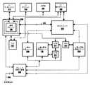
ここで図面、具体的には図1を参照すると、本発明の方法およびシステムの実施に使用することのできる、コンピュータ・データ処理システム10の高水準ブロック図が示されている。本発明を使用することのできるコンピュータ・データ処理システム10の主要なハードウェア構成要素および相互接続が、図1に示されている。命令を処理するための中央処理装置(CPU)100は、キャッシュ120、130および150に結合される。命令キャッシュ150には、CPU100による実行のための命令が格納される。データ・キャッシュ120には、CPU100によって使用されるデータが格納され、キャッシュ130には、CPU100によって使用されるデータおよび命令の両方を格納することができ、たとえば、キャッシュ130は、L2キャッシュとすることができる。キャッシュは、主記憶140内のランダム・アクセス・メモリと通信する。CPU100および主記憶140も、バス・インターフェース152を介してシステム・バス155と通信する。さまざまな入出力プロセッサ(IOP)160ないし168が、システム・バス155に付加され、直接アクセス記憶装置(DASD)170、テープ駆動装置172、遠隔通信回線174、ワークステーション176およびプリンタ178などのさまざまな記憶装置および入出力装置との通信をサポートする。図1は、高水準でコンピュータ・データ処理システム10の代表的な構成要素を示す目的のものであり、そのような構成要素の数と種類を変更できることを理解されたい。
【0043】
CPU100内では、プロセッサ・コア110に、特化した機能ユニットが含まれ、これらの機能ユニットのそれぞれが、命令のシーケンシング、整数を用いる演算の実行、実数を用いる演算の実行、アドレス可能記憶域と論理レジスタ・アレイの間の値の転送などのプリミティブ動作を実行する。図2は、コンピュータ・データ処理システム10の他の構成要素に関連するプロセッサ・コア110の詳細を示す図である。好ましい実施例では、データ処理システム10のプロセッサ・コア110は、単一集積回路のパイプライン式スーパースカラ・マイクロプロセッサであり、これは、たとえばIBM社によって販売されるPowerPC(商標)604マイクロプロセッサ・チップなど、商品名PowerPC(商標)の下で販売されるRISCプロセッサの系列などのコンピュータ・アーキテクチャを使用して実施できる。
【0044】
下で述べるように、データ処理システム10には、さまざまなユニット、レジスタ、バッファ、メモリおよび他のセクションが含まれることが好ましく、これらのすべてが集積回路によって形成されることが好ましい。図では、さまざまなデータ経路が簡略化されていることを理解されたい。実際には、さまざまな構成要素から出入りする多数の別々の並列のデータ経路がある。さらに、本明細書に記載の発明に密接に関係しないさまざまな構成要素が省略されているが、追加機能のためにプロセッサに追加ユニットが含まれることを理解されたい。データ処理システム10は、縮小命令セット・コンピューティング(RISC)技法または他のコンピューティング技法に従って動作することができる。
【0045】
図2からわかるように、データ処理システム10には、プロセッサ・コア110、レベル1データ・キャッシュ(L1 D−キャッシュ)120、レベル2(L2)キャッシュ130、遷移キャッシュ210、主記憶140およびレベル1命令キャッシュ(L1 I−キャッシュ)150が含まれることが好ましく、これらのすべてが、記憶域制御ユニット200へのさまざまなバス接続を使用して機能的に相互接続される。図2からわかるように、記憶域制御ユニット200には、L1 D−キャッシュ120およびL2キャッシュ130と、主記憶140と、複数の実行ユニットとを相互接続するための遷移キャッシュ210が含まれる。L1 D−キャッシュ120とL1 I−キャッシュ150は、プロセッサ100の一部としてチップ上に設けられることが好ましく、主記憶140とL2キャッシュ130は、チップ外に設けられる。メモリ・システム140は、プロセッサ・コア100の内部または外部とすることのできるランダム・アクセス・メイン・メモリ、プロセッサ・コア100の外部の他のデータ・バッファおよびキャッシュ(存在する場合)、および、たとえば図1に示されたDASD170、テープ駆動装置172、ワークステーション176などの他の外部メモリを表す目的のものである。L2キャッシュ130は、主記憶140より高速のメモリ・システムであることが好ましく、選択されたデータをL2キャッシュ130に格納することによって、主記憶140への参照の結果として発生するメモリ待ち時間を最小にすることができる。図2からわかるように、L2キャッシュ130および主記憶140は、L1 I−キャッシュ150に直接に、また記憶域制御ユニット200を介して命令ユニット220に接続される。
【0046】
図2からわかるように、L1 I−キャッシュ150からの命令は、命令ユニット220に出力されることが好ましく、命令ユニット220は、本発明の方法およびシステムに従って、さまざまなサブプロセッサ・ユニット、たとえば分岐ユニット260、固定小数点ユニット270、記憶域制御ユニット200、浮動小数点ユニット280および、データ処理システム10のアーキテクチャによって指定される他のユニットによる複数のスレッドの実行を制御する。当業者は、図2に示されたさまざまな実行ユニットのほかに、現代のスーパースカラ・マイクロプロセッサ・システムに、本発明の趣旨および範囲から逸脱せずに追加することのできるそのような実行ユニットのそれぞれの複数の版が含まれることがしばしばであることを了解するであろう。これらのユニットのほとんどは、入力として、汎用レジスタ(GPR)272および浮動小数点レジスタ(FPR)282などのさまざまなレジスタからのソース・オペランド情報を有する。さらに、複数の特殊目的レジスタ(SPR)274を使用することができる。図2からわかるように、記憶域制御ユニット200と遷移キャッシュ210は、汎用レジスタ272および浮動小数点レジスタ282に直接に接続される。汎用レジスタ272は、特殊目的レジスタ274に接続される。
【0047】
このマルチスレッド式プロセッサ100に固有の機能ハードウェア・ユニットの中に、スレッド切替え論理400と遷移キャッシュ210がある。スレッド切替え論理400には、どのスレッドをアクティブ・スレッドまたは実行中のスレッドにするかを決定するさまざまなレジスタが含まれる。スレッド切替え論理400は、機能的に、記憶域制御ユニット200と、実行ユニット260、270および280と、命令ユニット220に接続される。記憶域制御ユニット200内の遷移キャッシュ210は、マルチスレッディングを実施できなければならない。記憶域制御ユニット200と遷移キャッシュ210は、1スレッドあたり少なくとも1つの未処理のデータ要求を許容することが好ましい。したがって、たとえばL1 D−キャッシュ・ミスの発生に応答して、第1スレッドが延期される時に、第2スレッドが、そこに存在するデータについてL1 D−キャッシュ120にアクセスできるようになる。第2スレッドも、L1 D−キャッシュ・ミスをもたらす場合には、別のデータ要求が発行され、したがって、複数のデータ要求を、記憶域制御ユニット200および遷移キャッシュ210内で維持しなければならない。遷移キャッシュ210は、米国特許出願第08/761378号明細書の遷移キャッシュであることが好ましい。記憶域制御ユニット200と、実行ユニット260、270および280と、命令ユニット220は、すべてが機能的にスレッド切替え論理400に接続され、スレッド切替え論理400は、どのスレッドを実行するかを決定する。
【0048】
図2からわかるように、バス205は、たとえば記憶域制御ユニット200へのデータ要求および命令ユニット220へのL2キャッシュ130ミスなどの通信のために、記憶域制御ユニット200と命令ユニット220の間に設けられる。さらに、変換ルックアサイド・バッファ(TLB)250が設けられ、これには、仮想アドレスから実アドレスへのマッピングが格納される。図示されてはいないが、本発明では、変換ルックアサイド・バッファ250に類似の形で動作するセグメント・ルックアサイド・バッファなどの追加の高水準メモリ・マッピング・バッファを設けることができる。
【0049】
図3は、記憶域制御ユニット200を詳細に示す図であり、名前から暗示されるように、このユニットは、さまざまなキャッシュ、バッファおよび主記憶を含むさまざまな記憶ユニットからのデータおよび命令の入出力を制御する。図3からわかるように、記憶域制御ユニット200には、機能的にL1 D−キャッシュ120、マルチプレクサ360、L2キャッシュ130および主記憶140に接続された遷移キャッシュ210が含まれる。さらに、遷移キャッシュ210は、シーケンサ350から制御信号を受け取る。シーケンサ350には、命令またはデータの取出要求を処理するために、複数、好ましくは3つのシーケンサが含まれる。シーケンサ350は、遷移キャッシュ210およびL2キャッシュ130に制御信号を出力し、主記憶140との間で制御信号を送受する。
【0050】
図3に示された記憶域制御ユニット200内のマルチプレクサ360は、L1 D−キャッシュ120、遷移キャッシュ210、L2キャッシュ130および主記憶140からデータを受け取り、データをメモリに格納する場合には、実行ユニット270および280からデータを受け取る。これらの供給源のうちの1つからのデータは、マルチプレクサ360によって選択され、シーケンサ350から受け取った選択制御信号に応答して、L1 D−キャッシュ120または実行ユニットに出力される。さらに、図3からわかるように、シーケンサ350は、第2のマルチプレクサ370を制御する選択信号を出力する。シーケンサ350からのこの選択信号に基づいて、マルチプレクサ370は、L2キャッシュ130または主記憶140からのデータを、L1 I−キャッシュ150または命令ユニット220に出力する。上で述べた制御信号および選択信号を作る際に、シーケンサ350は、L1 D−キャッシュ120用のL1ディレクトリ320とL2キャッシュ130用のL2ディレクトリ330にアクセスし、これらを更新する。
【0051】
本明細書に記載のプロセッサのマルチスレッディング能力に関して、記憶域制御ユニット200のシーケンサ350は、スレッド切替え論理400にも信号を出力して、データ要求および命令要求の状態を示す。したがって、キャッシュ120、130および150と、主記憶140と、変換ルックアサイド・バッファ250からのフィードバックが、シーケンサ350に送られ、その後、スレッド切替え論理400に通信され、スレッド切替え論理400は、下で述べるようにスレッド切替えをもたらすことができる。マルチスレッド式プロセッサ内でのスレッド切替えを引き起こすように設計されたイベントが発生する装置は、機能的にスレッド切替え論理400に接続されることに留意されたい。
【0052】
図4は、スレッドを切り替えるかどうかを判定し、切り替える場合にはどのスレッドに切り替えるかを判定するスレッド切替え論理ハードウェア400の論理表現およびブロック図である。記憶域制御ユニット200と命令ユニット220は、スレッド切替え論理400と相互接続される。スレッド切替え論理400は、命令ユニット220に組み込まれることが好ましいが、多数のスレッドがある場合には、スレッド切替え論理400の複雑さが増し、その結果、スレッド切替え論理が命令ユニット220の外部になる場合がある。説明を簡単にするために、スレッド切替え論理400は、命令ユニット220の外部にあるものとして図示した。
【0053】
この実施例でスレッドの切替えをもたらすいくつかのイベントは、記憶域制御ユニット200のシーケンサ350からスレッド切替え論理400へ、信号線470、472、474、476、478、480、482、484および486を介して通信される。他の待ち時間イベントが、スレッド切替えを引き起こす可能性があるが、このリストは、網羅的であることを意図したものではなく、スレッド切替えを実施できる方法を代表するものにすぎない。命令ユニット220内にない第1スレッドT0または第2スレッドT1のいずれかによる命令の要求は、それぞれ図4の符号470または472によって示されるスレッド切替えをもたらす可能性があるイベントである。信号線474は、T0またはT1のいずれかであるアクティブ・スレッドが、L1 D−キャッシュ120ミスを経験する時を示す。スレッドT0またはT1のいずれかに関するL2キャッシュ130のキャッシュ・ミスは、それぞれ信号線476または478によって知らされる。信号線480および482は、それぞれT0スレッドまたはT1スレッドの継続実行のためにデータが返される時にアクティブになる。変換ルックアサイド・バッファ・ミスおよびテーブル・ウォークの完了は、それぞれ信号線484または486によって示される。
【0054】
これらのイベントは、すべてがスレッド切替え論理400に供給され、具体的には、スレッド状態レジスタ440およびスレッド切替えコントローラ450に供給される。スレッド切替え論理400は、スレッドごとに1つのスレッド状態レジスタを有する。本明細書に記載の実施例では、2つのスレッドが表現されるので、第1スレッド用T0のT0状態レジスタ442と、第2スレッドT1用のT1状態レジスタ444があり、これらを本明細書で説明する。スレッド切替え論理400には、どのイベントがスレッド切替えをもたらすかを制御するスレッド切替え制御レジスタ410が含まれる。たとえば、スレッド切替え制御レジスタ410は、状態変化がスレッド切替えコントローラ450によって見られるようにするイベントをブロックし、その結果、ブロックされたイベントの結果としてスレッドが切り替えられなくすることができる。スレッド切替え制御レジスタ410は、米国特許出願第08/958716号明細書の主題である。フォワード・プログレス・カウント・レジスタ420は、スラッシングの防止に使用され、スレッド切替え制御レジスタ410に含めることができる。フォワード・プログレス・カウント・レジスタ420は、米国特許出願第08/956875号明細書の主題である。スレッド切替えタイムアウト・レジスタ430は、米国特許出願第08/956577号明細書の主題であり、これによって、公平さとライブロック発行が割り振られる。またスレッド優先順位は、米国特許出願第08/958718号明細書の主題であるソフトウェア460を使用して変更することができる。制限的ではないが、最後に、スレッド切替えコントローラ450には、スレッドを切り替えるかどうかと、どのスレッドにどの状況の下で切り替えるのかを実際に判定するすべての論理の頂点を表す無数の論理ゲートが含まれる。これらの論理構成要素とその機能のそれぞれを、さらに詳細に説明する。
【0055】
スレッド状態レジスタ
スレッド状態レジスタ440には、各スレッドの状態レジスタが含まれ、名前からわかるように、対応するスレッドの状態が格納される。この例では、T0スレッド状態レジスタ442とT1スレッド状態レジスタ444がある。ビットの数と、各スレッドの状態を記述するための特定のビットの割振りは、特定のアーキテクチャおよびスレッド切替え優先順位方式に合わせてカスタマイズすることができる。2つのスレッドを有するマルチスレッド式プロセッサのスレッド状態レジスタ442および444のビットの割振りの例を、下の表に示す。
上で説明した実施例では、ビット0によって、ミスまたはプロセッサが実行をストールした理由が、命令のロードと、データのロードまたはストアとのどちらの要求の結果であるかが識別される。ビット1および2は、図5の説明でさらに説明するように、要求された情報が使用可能でなかったかどうかと、使用可能でなかった場合に、どのハードウェアから使用可能でなかったか、すなわち、データまたは命令の変換されたアドレスが変換ルックアサイド・バッファ250になかったのか、データまたは命令自体がL1 D−キャッシュ120またはL2キャッシュ130になかったのかを示す。ビット3は、スレッドの状態の変化が、スレッド切替えをもたらすかどうかを示す。スレッドは、スレッド切替えをもたらさずに状態を変更することができる。たとえば、スレッドT1がL1キャッシュ・ミスを経験する時にスレッド切替えが発生する場合に、スレッドT1がL2キャッシュ・ミスを経験する場合、L1キャッシュ・ミスの際にすでにスレッドが切り替えられているので、スレッド切替えはない。しかし、T1の状態は、まだ変化する。その代わりに、選択によって、スレッド切替え論理400が、L1キャッシュ・ミスの際に切り替えないように構成またはプログラミングされる場合には、スレッドがL1キャッシュ・ミスを経験した時に、スレッドの状態が変化してもスレッド切替えはない。スレッド状態レジスタ442および444のビット8は、特定のスレッドによって要求された情報が、プロセッサ・コアにロードされるのか、プロセッサ・コアからキャッシュまたは主記憶にストアされるのかに割り当てられる。ビット15ないし17は、フォワード・プログレス・カウント・レジスタ420に関して後で説明するように、スラッシングの防止に割り振られる。ビット18および19は、スレッドの優先順位を示すために、ハードウェアで設定するか、ソフトウェアによって設定することができる。
【0057】
図5は、データ処理システム10によって処理されるスレッドの現在の実施例での4つの状態を表し、これらの状態は、スレッド状態レジスタ440のビット位置1:2に格納される。状態00は、「実行可能」状態すなわち、必要なすべてのデータおよび命令が使用可能であるので、スレッドの処理の準備ができていることを表す。状態10は、スレッドがL1 D−キャッシュ120にデータが返されるかL1 I−キャッシュ150に命令が返されるかのいずれかを待っているので、プロセッサ内でのスレッドの実行がストールしているスレッド状態を表す。状態11は、スレッドがL2キャッシュ130にデータが返されるのを待っていることを表す。状態01は、テーブル・ウォークと称する、変換ルックアサイド・バッファ250でのミスがある、すなわち、仮想アドレスがエラー状態であったか、使用可能でなかったことを示す。図5には、スレッド状態の階層も示されており、スレッドの実行の準備ができていることを示す状態00が、最も高い優先順位を有する。短い待ち時間イベントには、高い優先順位を割り当てることが好ましい。
【0058】
図5には、データがさまざまな供給源から取り出される時の状態の変化も示されている。スレッドT0の通常の割り込みのない(uninterrupted)実行は、ブロック510で状態00として表されている。L1 D−キャッシュまたはI−キャッシュのミスが発生した場合、スレッドの状態は、記憶域制御ユニット200からの信号線474(図4)または命令ユニット220からの信号線470(図4)で送られる信号に従って、ブロック512に示されている状態10に変化する。要求されたデータまたは命令が、L2キャッシュ130内にあり、取り出される場合には、ブロック510のT0の通常の実行が再開される。同様に、図5のブロック514は、L2キャッシュ・ミスを表し、これによって、T0またはT1のいずれかのスレッドの状態が、記憶域制御ユニット200が信号線476または478(図4)でミスの信号を送る時に、状態11に変化する。信号線480および482(図4)に示されているように、L2キャッシュ内の命令またはデータが、主記憶140から取り出され、プロセッサ・コア100にロードされる時には、状態は、やはりブロック510の状態00に戻る。要求された情報の仮想アドレスが変換ルックアサイド・バッファ250内で使用可能でない時には、ブロック516に示されるように、TLBミスまたは状態01として、記憶域制御ユニット200が、信号線484(図4)を介してスレッド・レジスタ440に通信する。そのアドレスが使用可能になる時または、信号線486(図4)上で記憶域制御ユニット200によって送られるデータ記憶域割り込み命令がある場合には、スレッドの状態は、状態00に戻り、実行の準備ができる。
【0059】
状態の数と、各状態が表すものは、コンピュータ設計者が自由に選択できる。たとえば、あるスレッドが、L1 I−キャッシュ・ミスとL1 D−キャッシュ・ミスなど、複数のL1キャッシュ・ミスを有する場合には、キャッシュ・ミスのタイプのそれぞれに別々の状態を割り当てることができる。その代わりに、単一のスレッド状態を割り当てて、複数のイベントまたはできごとを表すことができる。
【0060】
等しい優先順位を有する2つのスレッドについて、スレッドを切り替えるかどうかを判定するスレッド切替えアルゴリズムの例を示す。このアルゴリズムは、本発明の教示に従って、より多くのスレッドおよびスレッド切替え条件のためにそれ相応に拡張し、変更することができる。スレッド切替えアルゴリズムによる、スレッド状態レジスタ440(図4)に格納された各スレッドの状態と各スレッドの優先順位との間の相互作用は、各サイクルに動的に問い合わされる。アクティブ・スレッドT0がL1ミスを有する場合に、このアルゴリズムは、休止スレッドT1がL2ミスの解決を待っている場合を除いて、休止スレッドT1へのスレッド切替えを引き起こす。切替えが発生せず、アクティブ・スレッドT0のL1キャッシュ・ミスがL2キャッシュ・ミスになった場合には、このアルゴリズムは、プロセッサに、T1の状態に無関係に休止スレッドT1に切り替えるように指示する。両方のスレッドがL2キャッシュ・ミスの解決を待っている場合には、最初にL2ミスを解決されたスレッドが、アクティブ・スレッドになる。すべての切替え決定時に、行われる処置は、最も可能性の高い事例に合わせて最適化され、最良の性能をもたらす。L2キャッシュ・ミスから生じるスレッド切替えは、性能の低下をもたらす余分なスレッド切替えが発生しない場合に、他方のスレッドの状態次第である。
【0061】
スレッド切替え制御レジスタ
どのマルチスレッド式プロセッサにも、スレッド切替えに関連する待ち時間と性能のペナルティが存在する。本明細書で説明する好ましい実施例のマルチスレッド式プロセッサでは、この待ち時間に、現在のスレッドに割り込むことができ、現在のスレッドが次に呼び出された時に正しく再始動できる点まで現在のスレッドの実行を完了するのに必要な時間と、スレッド固有のハードウェア機能を現在のスレッドの状態から新しいスレッドの状態に切り替えるのに必要な時間と、新しいスレッドを再始動し、その実行を開始するのに必要な時間が含まれる。本発明と共に動作可能なスレッド固有のハードウェア機能には、上で説明したスレッド状態レジスタと、米国特許第5778243号明細書に記載のメモリ・セルが含まれることが好ましい。粒度の粗いマルチスレッド式データ処理システムで最適の性能を達成するために、スレッド切替えを生成するイベントの待ち時間は、通常の単一スレッド・モードに対して、マルチスレッド・モードでのスレッド切替えに関連する性能コストより大きくなければならない。
【0062】
スレッド切替えを生成するのに使用されるイベントの待ち時間は、ハードウェアとソフトウェアの両方に依存する。たとえば、マルチスレッド式プロセッサの特定のハードウェア検討事項には、プロセッサ・チップの外部のL2キャッシュの実施に使用される外部SRAMの速度が含まれる。L2キャッシュのSRAMが高速になると、L1ミスの平均待ち時間が減るが、SRAMが低速になると、L1ミスの平均待ち時間が増える。したがって、あるスレッド切替えイベントが、スレッド切替えのペナルティより大きい外部L2キャッシュ・データ・アクセス待ち時間を有するハードウェアのL1キャッシュ・ミスとして定義される場合に、高性能が得られる。特定のソフトウェア・コードの特性が、スレッド切替えイベントの待ち時間にどのように影響するかの例として、コードのL2キャッシュのヒット対ミス比すなわち、データがL2キャッシュにないので主記憶から取り出さなければならない回数と比較した、データが実際にL2キャッシュ内で使用可能である回数を検討されたい。L2ヒット対ミス比が高いと、L1キャッシュ・ミスが、より長い待ち時間のL2ミスをほとんどもたらさないので、L1キャッシュ・ミスの平均待ち時間が減る。L2ヒット対ミス比が低いと、より長い待ち時間のL2ミスをもたらすL1ミスが増えるので、L1ミスの平均待ち時間が増える。したがって、実行中のコードが高いL2ヒット対ミス比を有する場合には、L2キャッシュ・データ・アクセス待ち時間がスレッド切替えペナルティより小さいので、スレッド切替えイベントとしてのL1ミスを使用不能にすることができる。低いL2ヒット対ミス比を有するソフトウェア・コードを実行する時には、L1キャッシュ・ミスが、より長い待ち時間のL2キャッシュ・ミスになる可能性が高いので、L1キャッシュ・ミスをスレッド切替えイベントとして使用可能にすることになる。
【0063】
いくつかのタイプの待ち時間イベントは、簡単には検出できない。たとえば、いくつかのシステムでは、キャッシュ・ミスが発生した時に、L2キャッシュが、命令ユニットに信号を出力する。しかし、他のL2キャッシュは、たとえばL2キャッシュ・コントローラがプロセッサとは別のチップ上にあり、したがって、プロセッサが状態変化を簡単に判定できない場合に、そのような信号を出力しない。これらのアーキテクチャでは、プロセッサに、未処理のL1キャッシュ・ミスごとに1つのサイクル・カウンタを含めることができる。所定のサイクル数の前にミス・データがL2キャッシュから返されない場合には、プロセッサは、L2キャッシュ・ミスがあったかのように動作し、スレッドの状態をそれ相応に変更する。このアルゴリズムは、複数の別個のタイプの待ち時間が存在する他の場合にも適用可能である。例のみとして、プロセッサでのL2キャッシュ・ミスの場合、主記憶からのデータの待ち時間は、別のプロセッサからのデータの待ち時間と大きく異なる場合がある。これらの2つのイベントに、スレッド状態レジスタ内で異なる状態を割り当てることができる。これらの状態を区別する信号が存在しない場合には、カウンタを使用して、スレッドがL2キャッシュ・ミスに遭遇した後に、スレッドがどの状態にならなければならないかを推定することができる。
【0064】
スレッド切替え制御レジスタ410は、スレッド切替えを生成するイベントを選択するソフトウェア・プログラム可能レジスタであり、定義されたスレッド切替え制御イベントのそれぞれについて別々のイネーブル・ビットを有する。本明細書で説明する実施例では、スレッドごとに別々のスレッド切替え制御レジスタ410は実施されないが、スレッドごとに別々のスレッド切替え制御レジスタ410を実施して、より多くのハードウェアおよび複雑さという犠牲と引き換えにより高い柔軟性と性能をもたらすことができる。さらに、あるスレッド切替え制御レジスタ内のスレッド切替え制御イベントは、他のスレッド切替え制御レジスタのスレッド切替え制御イベントと同一である必要はない。
【0065】
スレッド切替え制御レジスタ410は、米国特許第5079725号明細書に開示された動的走査通信インターフェースなどのソフトウェアを用いるサービス・プロセッサによるか、ソフトウェア・システム・コードを用いてプロセッサ自体によって、書き込むことができる。スレッド切替え制御レジスタ410の内容は、スレッド切替えの生成を使用可能または使用不能にするために、スレッド切替えコントローラ450によって使用される。レジスタ410内の1の値によって、そのビットに関連するスレッド切替え制御イベントが使用可能にされて、スレッド切替えが生成される。スレッド切替え制御レジスタ410内の0の値によって、そのビットに関連するスレッド切替え制御イベントが、スレッド切替えの生成を禁止される。もちろん、実行中のスレッド内の命令によって、その特定のスレッドまたは他のスレッドのスレッド切替え条件のうちのいくつかまたはすべてを使用不能にすることができる。下の表に、スレッド切替えイベントと、レジスタ410内のイネーブル・ビットの間の関連を示す。
スレッド切替え制御レジスタのビット割当
(0) L1データ・キャッシュ取出ミスに対するスイッチ
(1) L1データ・キャッシュ・ストア・ミスに対するスイッチ
(2) L1命令キャッシュ・ミスに対するスイッチ
(3) 命令TLBミスに対するスイッチ
(4) L2キャッシュ取出ミスに対するスイッチ
(5) L2キャッシュ・ストア・ミスに対するスイッチ
(6) L2命令キャッシュ・ミスに対するスイッチ
(7) データTLB/セグメント・ルックアサイド・バッファ・ミスに対するスイッチ
(8) L2キャッシュ・ミスおよび休止スレッド非L2キャッシュ・ミスに対するスイッチ
(9) スレッド切替えタイムアウト値到達時のスイッチ
(10) L2キャッシュ・データが返された時のスイッチ
(11) 入出力外部アクセスに対するスイッチ
(12) ダブルXストア:2つのうちの1番目でのミスに対するスイッチ*
(13) ダブルXストア:2つのうちの2番目でのミスに対するスイッチ*
(14) 複数/列ストア:すべてのアクセスでのミスに対するスイッチ
(15) 複数/列ロード:すべてのアクセスでのミスに対するスイッチ
(16) 予約済み
(17) ダブルXロード:2つのうちの1番目でのミスに対するスイッチ*
(18) ダブルXロード:2つのうちの2番目でのミスに対するスイッチ*
(19) 計算機状態レジスタ(問題状態)ビット、msr(pr)=1の場合のor 1,1,1命令に対するスイッチ。msr(pr)と独立のソフトウェア優先順位変更を可能にする。ビット19が1の場合、or 1,1,1命令によって低優先順位が設定される。ビット19が0の場合、or 1,1,1命令が実行される時にmsr(pr)=0の場合に限って優先順位が低に設定される。後で説明する、ソフトウェアによる優先順位の変更を参照されたい。
(20) 予約済み
(21) スレッド切替え優先順位イネーブル
(22:29) 予約済み
(30:31) フォワード・プログレス・カウント
(32:63) 64ビット・レジスタ実施形態で予約済み
*ダブルXロード/ストアとは、基本ハーフワード、ワードまたはダブル・ワードの、ダブルワード境界をまたぐロードまたはストアを指す。この文脈でのダブルXロード/ストアは、複数ワードまたはワードの列のロードまたはストアではない。
【0066】
スレッド切替えタイムアウト・レジスタ
上で述べたように、粒度の粗いマルチスレッド式プロセッサは、スレッド切替えをトリガするために、長い待ち時間のイベントに頼る。実行中に、多重プロセッサ環境内のプロセッサまたはマルチスレッド式アーキテクチャのバックグラウンド・スレッドが、単独の所有者だけを有することのできる資源の所有権を有し、別のプロセッサまたはアクティブ・スレッドが、フォワード・プログレスを行う前にその資源へのアクセスを必要とする場合がある。その例には、メモリ・ページ・テーブルの更新またはタスク・ディスパッチャからのタスクの取得が含まれる。アクティブ・スレッドが資源の所有権を得ることができなくても、スレッド切替えイベントはもたらされないが、スレッドは、有用な作業を行うことができないループを回り続ける。この場合、資源を保持しているバックグラウンド・スレッドは、プロセッサへのアクセスを得ず、その結果、スレッド切替えイベントに遭遇せず、アクティブ・スレッドにならないので、資源を解放することができない。
【0067】
スレッドの間での処理サイクルの割振りが、もう1つの問題である。あるスレッド上で走行するソフトウェア・コードが、同一のプロセッサ内の他のスレッド上で走行するソフトウェア・コードと比較して長い待ち時間の切替えイベントにほとんど遭遇しない場合には、そのスレッドは、処理サイクルの公平な割当分以上の処理サイクルを得る。最大の許容可能な時間を超える可能性があるもう1つの過度な遅延が、限られた時間期間内に外部割込みをサービスするために待機するかプロセッサの外部の他のイベントを待機する非アクティブ・スレッドの待ち時間である。したがって、有用な処理が達成されていない場合に、システムがハングしないようにするために、ある時間の後に休止スレッドへのスレッド切替えを強制的に行うことが好ましくなる。
【0068】
ある時間期間の後にスレッド切替えを強制するための論理が、スレッド切替えタイムアウト・レジスタ430(図4)、デクリメンタおよび、減分された値を保持する減分レジスタである。スレッド切替えタイムアウト・レジスタ430は、スレッド切替えタイムアウト値を保持する。この実施例で使用されるスレッド切替えタイムアウト・レジスタ430の実施形態を、次の表に示す。
スレッド切替えタイムアウト・レジスタのビット
(0:21) 予約済み
(22:31) スレッド切替えタイムアウト値
【0069】
本明細書で説明する本発明の実施例では、スレッドごとに別々のスレッド切替えタイムアウト・レジスタ430が実施されないが、柔軟性を高めるためにそれを行うことは可能である。同様に、複数のスレッドがある場合に、各スレッドが同一のスレッド切替えタイムアウト値を有する必要はない。スレッド切替えが発生するたびに、スレッド切替えタイムアウト・レジスタ430からのスレッド切替えタイムアウト値が、ハードウェアによって減分レジスタにロードされる。減分レジスタは、減分レジスタ値が0に等しくなるまで各サイクルに1回減分され、0になった時に、スレッド切替えコントローラ450に信号が送られ、スレッド切替えコントローラ450は、命令を処理する準備ができている他のスレッドがない場合を除いて、スレッド切替えを強制する。たとえば、システム内の他のすべてのスレッドが、キャッシュ・ミスで待機状態になっており、命令を実行する準備ができていない場合には、スレッド切替えコントローラ450は、スレッド切替えを強制しない。減分レジスタの値が0に達した時に、命令を処理する準備ができている他のスレッドが存在しない場合には、別のスレッドが命令を処理する準備ができるまで、減分された値は0で凍結され、準備ができた時点で、スレッド切替えが発生し、減分レジスタに、そのスレッドのスレッド切替えタイムアウト値が再ロードされる。同様に、減分レジスタは、簡単に増分レジスタと命名することができ、スレッドが実行中である時に、そのレジスタをある所定の値まで増分することができ、その値に達した時にスレッド切替えが強制される。
【0070】
スレッド切替えタイムアウト・レジスタ430は、上で述べたようにサービス・プロセッサによって書き込むか、ソフトウェア・コードを用いてプロセッサ自体によって書き込むことができる。スレッド切替えタイムアウト・レジスタ430にロードされるスレッド切替えタイムアウト値は、特定のハードウェア構成または特定のソフトウェア・コードに従って、不要なスレッド切替えから生じる浪費サイクルを最小にするためにカスタマイズすることができる。スレッド切替えタイムアウト・レジスタ430の値が大きすぎると、アクティブ・スレッドが別のスレッドによって保持されている資源を待っている場合と、外部割込み290または他のプロセッサ外部のイベントの応答待ち時間が長すぎる場合に、性能低下がもたらされる可能性がある。また、値が大きすぎると、一方のスレッドが多数のスレッド切替えイベントを経験し、もう一方のスレッドがそうでない場合に、公平さが損なわれる可能性がある。スレッド切替えを引き起こす、最も頻繁な最長の待ち時間イベント、たとえば主記憶へのアクセスより2倍ないし数倍長いスレッド切替えタイムアウト値が、推奨される。スレッド切替えタイムアウト・レジスタ430で指定されたサイクル数だけ待った後にスレッド切替えを強制することによって、共用資源の競合に起因するシステム・ハングが防止され、スレッド間のプロセッサ・サイクル割振りの公平さが実施され、外部割り込みおよび他のプロセッサ外部のイベントに対する最大応答待ち時間が制限される。
【0071】
フォワード・プログレスの保証
スレッド切替えが発生し、新しいスレッドがアクティブになるたびに、少なくとも1つの命令が実行されなければならないことは、単一の命令によって複数のキャッシュ・アクセスまたは複数のキャッシュ・ミスが発生する時など、いくつかの状況では制限が強すぎる。たとえば、取出命令は、要求された命令がキャッシュ内にない場合にL1 I−キャッシュ150ミスを引き起こす可能性があるが、その命令が返された時に、必要なデータがL1 D−キャッシュ120内で使用可能でない可能性がある。同様に、変換ルックアサイド・バッファ250でのミスが、データ・キャッシュ・ミスをももたらす可能性がある。したがって、フォワード・プログレスを厳密に実施する場合には、後続アクセスでのミスは、スレッド切替えをもたらさない。第2の問題は、一部のキャッシュ・ミスが、完了に大量のサイクルを必要とする可能性があり、その時間の間に、別のスレッドが、同一のキャッシュ・レベルで、はるかに短い時間で完了できるキャッシュ・ミスを経験する可能性があることである。第1のスレッドに戻る時に、厳密なフォワード・プログレスが実施される場合には、プロセッサは、より短いキャッシュ・ミスを有するスレッドに切り替えることができない。
【0072】
各スレッドが、命令実行を伴わないスレッド切替えの反復サイクルでロックされるスラッシングの問題を救済するために、フォワード・プログレス・カウント・レジスタ420(図4)が存在し、これによって、フォワード・プログレス閾値と称するプログラム可能な最大回数までのスレッド切替えが許容される。そのスレッド切替えの最大回数の後は、命令を完了しなければ切替えは発生しない。この形で、スラッシングが防止される。フォワード・プログレス・カウント・レジスタ420は、実際には、スレッド切替え制御レジスタ410のビット30:31とするか、プロセッサのためのソフトウェア・プログラム可能フォワード・プログレス閾値レジスタとすることができる。フォワード・プログレス・カウント論理は、スレッドの状態を示し、命令実行なしでスレッドが経験したスレッド切替えの回数のために割り振られる、スレッド状態レジスタ442および444のビット15:17を使用する。これらのビットは、フォワード・プログレス・カウンタを含むことが好ましい。
【0073】
スレッドの状態が変化し、スレッド切替えアルゴリズムが呼び出される時に、アクティブ・スレッド内で少なくとも1つの命令が完了している場合、アクティブ・スレッドのフォワード・プログレス・カウンタは、リセットされ、スレッド切替えアルゴリズムは、プロセッサ内のスレッドの間でのスレッド状態の比較を継続する。完了した命令がない場合、アクティブ・スレッドのスレッド状態レジスタ内のフォワード・プログレス・カウンタ値が、フォワード・プログレス閾値と比較される。カウンタ値が、閾値と等しくない場合には、スレッド切替えアルゴリズムは、プロセッサ内のスレッドのスレッド状態の評価を継続する。その後、スレッド切替えが発生した場合に、フォワード・プログレス・カウンタが増分される。しかし、カウンタ値が閾値または状態と等しい場合には、命令を実行できるまで、すなわち、フォワード・プログレスが発生するまで、スレッド切替えは発生しない。閾値レジスタが値0を有する場合には、別のスレッドに切り替える前に、アクティブ・スレッド内で少なくとも1つの命令が完了しなければならないことに留意されたい。各スレッド切替えが、3プロセッサ・サイクルを必要とし、2つのスレッドが存在し、スレッド切替え論理が、5回の試行の値にスレッド切替えの試行を停止するようにプログラミングされている場合、プロセッサのスラッシングが発生する最大サイクル数は、30サイクルである。当業者は、一方でフォワード・プログレスが行われないのでスレッド切替えを禁止することと、他方でタイムアウト・カウントを超えたのでスレッド切替えを強制することの間に潜在的な衝突が存在することを了解するであろう。このような衝突は、アーキテクチャおよびソフトウェアに従って簡単に解決することができる。
【0074】
図6は、スラッシングを防止する、スレッド切替え論理400のフォワード・プログレス・カウント機能の流れ図である。ブロック610で、スレッドT0に関係するスレッド状態レジスタ442のビット15:17が、状態111にリセットされる。ブロック620で、このスレッドの実行を試み、状態が000に変化する。スレッドT0で命令が成功裡に実行された場合、スレッドT0の状態は、111に戻り、そのままにとどまる。しかし、スレッドT0が命令を実行できない場合には、スレッドT1または、プロセッサ・アーキテクチャで3つ以上のスレッドが許容される場合には別のバックグラウンド・スレッドへのスレッド切替えが発生する。T1または他のバックグラウンド・スレッドからのスレッド切替えが発生し、実行がスレッドT0に戻った時に、ブロック630で、スレッドT0を実行する2回目の試みが行われ、スレッドT0の状態は001になる。やはり、スレッドT0がスレッド切替えイベントに遭遇した場合に、プロセッサの制御は、スレッドT0から別のスレッドに切り替えられる。同様に、たとえばT1などの他のスレッドからスレッドT0へのスレッド切替えが発生した時に、T0の状態は、T0実行の3回目の試みでは010に変化し(ブロック640)、T0実行の4回目の試みでは011に変化し(ブロック650)、T0実行の5回目の試みでは状態100に変化する(ブロック660)。
【0075】
この実施形態では、スレッドT0への切替えの試みが5回ある。5回目の試みの後と、スレッド状態レジスタ(TSR)442のビット15:17の値が、スレッド切替え制御レジスタ(TSC)410のビット30:31の値+1に等しい時すなわち、TSC(30:31)+1=TSR(15:17)の時に必ず、スレッドT0からのスレッド切替えが発生しなくなる。5回の試みは、任意の数であり、不成功の実行を伴う切替えの許容可能な最大回数すなわち、フォワード・プログレス閾値は、プログラム可能であることが了解されよう。また、あるアーキテクチャでは、5回の切替えが多すぎ、他のアーキテクチャでは5回が少なすぎることが理解されよう。どの場合でも、命令実行なしでスレッドに切り替える試みの回数の間の関係を閾値と比較しなければならず、その閾値に達した後には、そのスレッドからのスレッド切替えが発生せず、プロセッサは、そのスレッドに関連する待ち時間が解決されるまで待機する。本明細書で説明する実施例では、スレッド状態レジスタ442のビット15:17によって表されるスレッドの状態が、スレッド切替え制御レジスタ410のビット30:31と比較される。フォワード・プログレス論理による早すぎるスレッド切替えのブロックを防ぐための、入出力装置との相互作用などの極端に長い待ち時間を有する特定のイベントのための特別な処理によって、プロセッサ性能が改善される。これらの極端に長い待ち時間のイベントを処理する方法の1つが、フォワード・プログレス・カウンタの増分をブロックするか、データが返されなかった場合のフォワード・プログレス・カウンタと閾値の間の比較の出力信号を無視することである。極端に長い待ち時間のイベントを処理するもう1つの方法は、これらの特定のイベントについて、別のより大きいフォワード・プログレス・カウントを使用することである。
【0076】
スレッド切替えマネージャ
プロセッサにディスパッチされたすべてのソフトウェア・スレッドのスレッド状態は、前に説明したように図4のスレッド状態レジスタ442および444で維持されることが好ましい。単一のプロセッサでは、一時に1つのスレッドがその命令を実行し、他のすべてのスレッドは、休止状態になる。実行がアクティブ・スレッドから休止スレッドに切り替えられるのは、アクティブ・スレッドが、フォワード・プログレス・レジスタ420、スレッド切替え制御レジスタ410またはスレッド切替えタイムアウト・レジスタ430に関して上で説明した長い待ち時間のイベントに出会った時である。どのスレッドがアクティブであるかに無関係に、これらのハードウェア・レジスタでは、実行の過程の間に動的に変化しない状態が使用される。
【0077】
スレッド切替えマネージャによってスレッド切替え条件を変更する柔軟性によって、総合的なシステム性能が改善される。ソフトウェア・スレッド切替えマネージャは、スレッド切替えの頻度を変更でき、クリティカルなタスクが使用できる実行サイクルを増やすことができ、スレッド切替え待ち時間のために失われる総合サイクルを減らすことができる。スレッド切替えマネージャは、コンパイル時または、オペレーティング・システムによる実行中のいずれかにプログラミングすることができ、たとえば、ロックしているループからスレッド切替えの頻度を変更でき、また、低い優先順位状態の休止スレッドが外部割込みを待っているか他の形で作動可能であるのでオペレーティング・システム・タスクをディスパッチすることができる。アクティブ・スレッドからのスレッド切替えを許容しないか、その頻度を減らし、その結果、現在の命令ストリームの性能が、そこからの切替えとそこに戻る切替えから生じる待ち時間を被らなくすることが有利である場合がある。その代わりに、スレッドが、総合的なシステム性能を強化するために、本質的にその優先順位を下げ、その結果として、それへの切替えの頻度を下げるか、そのスレッドからの切替えの頻度を高めることによって、その実行サイクルの一部またはすべてを捨てることができる。スレッド切替えマネージャは、スレッド切替えを無条件で強制または禁止することもでき、どのスレッドが次に実行のために選択されるかに影響することもできる。
【0078】
複数優先順位スレッド切替え方式では、各スレッドに優先順位値を割り当てて、切替えを引き起こす条件を制限する。場合によっては、ハードウェアにスレッド優先順位を変更させることが望ましい可能性もある。たとえば、低優先順位スレッドが、あるイベントを待っており、そのイベントが発生した時に、ハードウェアが、そのスレッドの優先順位を引き上げて、外部割込み290などのイベントに対するそのスレッドの応答時間に影響することができる。スレッド間の相対優先順位またはあるスレッドの優先順位は、そのようなイベントの処理に影響する。スレッドの優先順位は、イベントに応答してハードウェアによって、または、1つまたは複数の命令の使用を介してスレッド切替えマネージャソフトウェアによって、調節することができる。スレッド切替えマネージャは、ハードウェア・スレッド切替え論理によって実行される処置を変更して、効果的にスレッドの相対優先順位を変更する。
【0079】
3つの優先順位が、本明細書で説明する2スレッドの実施例と共に使用され、これによって、システム性能に悪影響を及ぼさずに、性能のチューニングを可能にするのに十分な、スレッドの間の区別がもたらされる。3つの優先順位を用いると、2つのスレッドが、中優先順位の同等の状況を有することができる。2つのスレッドに関する3つの優先順位の選択は、制限的であることを目的とするものではない。いくつかのアーキテクチャでは、「通常」状態が、一方のスレッドが必ず他方のスレッドより高い優先順位を有する状態であるものとすることができる。ハードウェアで設定するかソフトウェアによってプログラミングすることのできる1つまたは複数の優先順位を有する3つ以上の実行のスレッドを含むことが、本発明の範囲内であることが意図されている。
【0080】
各スレッドの3つの優先順位は、高、中および低である。スレッドT0の優先順位がスレッドT1と同一である時には、スレッド切替え論理に対する影響はない。両方のスレッドが等しい優先順位を有するので、優先的に実行時間を与えられるスレッドは存在しない。スレッドT0の優先順位が、スレッドT1の優先順位より高い時には、T0からT1へのスレッド切替えイベントは、あるスレッド切替えイベントすなわち、すべてのL1キャッシュ・ミスすなわち、データ・ロード、データ・ストアおよび命令取出について使用不能にされる。というのは、L1キャッシュ・ミスが、L2ミスおよび変換などの他の条件よりはるかに高速に解決されるからである。どのスレッド切替えイベントでも、使用不能にし、その結果、スレッドT0に、スレッドT1より多数の実行サイクルを受け取る機会を与えることができ、これによって、スレッドT0が、過剰な数の実行サイクルを浪費しない限り、実行を継続できるようになる。しかし、プロセッサは、スレッドT0が比較的長い実行待ち時間、たとえば、L2キャッシュ・ミスまたはコンピュータ・システムの外部の供給源からのデータの取出などを経験する場合に、スレッドT1に制御を譲る。T1からT0へのスレッド切替えは、休止スレッドT0がスレッドT1をプリエンプトした場合にスレッドT0が作動可能になった時に切替えが発生する点を除いて、影響を受けない。この事例は、L2キャッシュ・ミスまたは変換要求が原因でスレッドT0からの切替えが発生し、その条件が、スレッドT1の実行中にバックグラウンドで解決された時に発生すると予想される。スレッドT0がスレッドT1より低い優先順位を有する場合は、上の場合でスレッドの指定を逆転したものに類似する。
【0081】
スレッド優先順位の変更によるスレッド切替えの管理を実装することができる異なる手法が存在する。新しい命令をプロセッサ・アーキテクチャに追加することができる。所望の動作を有する副作用を有する既存のプロセッサ命令を使用することもできる。ソフトウェア制御を可能にする方法の間での選択に影響する要因には、以下が含まれる。(a)新規命令を含めるためのアーキテクチャ再定義の容易さと、既存プロセッサに対するアーキテクチャ変更の影響、(b)異なる版のプロセッサ上で同一のソフトウェアを走行させることの望ましさ、(c)新規の専用命令の使用と、既存命令を再利用し結果の副作用を定義することとの間の性能トレードオフ、(d)たとえば、特定のロードまたはストアなどの一部の既存命令のすべての実行によって効果が生じるか、特にその効果を生じさせるためにストリームに命令を追加することによるさらなる制御を必要とするか、など、ソフトウェアによる制御の所望のレベル。
【0082】
本明細書で説明するアーキテクチャは、その値によってプロセッサのアーキテクチャ的汎用レジスタが変更されない、未使用命令を活用する。この機能は、プロセッサ・アーキテクチャを更新してマルチスレッディング機能を組み込むのに非常に重要である。そうでなければ、特殊命令をコーディングすることができる。命令は、「好ましいノー・オペレーション」or 0,0,0であるが、他の命令が、効果的にノー・オペレーションとして働くことができる。ノー・オペレーションまたはnopは、その実行が、コンピュータに、動作を実行せずに次の命令の実行に進行させる命令である。好ましいアーキテクチャの実施例では、or命令の異なる版、or 0,0,0または1,1,1か、スレッド優先順位を変更するために追加の優先順位切替えの意味を付加することのできる既存命令を使用することによって、同一の命令ストリームを、不正命令割込みなどの悪影響なしにプロセッサ上で実行することができる。不正命令割込みは、不正命令の実行が試みられる時または、実施形態によって提供されない予約済みまたは任意選択の命令の実行が試みられる時に生成される。機能拡張では、計算機状態レジスタの状態を使用して、これらの命令の意味を変更する。たとえば、ユーザがこれらのスレッド優先順位命令の一部またはすべてをコーディングし、それらが提供する機能にアクセスできるようにすることは、望ましくない場合がある。それらが提供する特殊機能は、実行のあるモードだけで発生するように定義することができ、それらの命令は、他のモードでは効果がなく、通常通りノー・オペレーションとして実行される。
【0083】
二重スレッド・マルチスレッド式プロセッサを使用する可能な実施形態の1つでは、実行中のソフトウェア自体の一部になる下記の3つの優先順位切替え命令を使用して、それ自体の優先順位を変更する。
優先順位切替え命令tsop 1およびtsop 2は、本明細書でor 1,1,1として実施されるものと同一の命令とすることができるが、これらを別々の命令とすることもできる。これらの命令は、スレッド切替え制御レジスタ410のビット19および21と、本明細書で説明した計算機状態レジスタの問題/優先順位ビットとに相互作用する。スレッド切替え制御レジスタ410のビット21が1の値を有する場合には、スレッド切替えマネージャは、そのスレッドの優先順位に、スレッド状態レジスタのビット18:19で表される3つの優先順位のうちの1つをセットすることができる。スレッド切替え制御レジスタ410のビット19が値0を有する場合には、命令tsop 2のスレッド切替えおよびスレッド優先順位の設定は、計算機状態レジスタの問題/優先順位ビットによって制御される。その一方で、スレッド切替え制御レジスタ410のビット19が値1を有する場合または、計算機状態レジスタの問題/優先順位ビットが値0を有し、命令or 1,1,1がコードに存在する場合には、アクティブ・スレッドの優先順位は、低に設定され、実行は、休止スレッドがイネーブルされる場合に即座に休止スレッドまたはバックグラウンド・スレッドに切り替えられる。命令or 2,2,2では、アクティブ・スレッドの優先順位が、計算機状態レジスタの問題/優先順位ビットの値に無関係に中に設定される。命令or 3,3,3では、計算機状態レジスタの問題/優先順位ビットが0の値を有する時に、アクティブ・スレッドの優先順位に高がセットされる。スレッド切替え制御レジスタ410のビット21が0の場合、両方のスレッドの優先順位に、中がセットされ、優先順位に対するor x,x,xの影響がブロックされる。外部割込み要求がアクティブであり、対応するスレッドの優先順位が低の場合、そのスレッドの優先順位は、中に設定される。
【0085】
スレッド優先順位によって変更されるイベントは、(1)データをロードする際のL1 D−キャッシュ・ミスに対するスイッチと、(2)データをストアする際のL1 D−キャッシュ・ミスに対するスイッチと、(3)命令を取り出す際のL1 I−キャッシュ・ミスに対するスイッチと、(4)休止スレッドが作動可能状態である場合のスイッチである。さらに、外部割込みの活動化によって、対応するスレッドの優先順位を変更することができる。下の表に、スレッド切替えを引き起こす条件に対する優先順位の影響を示す。列3および4の「TSC」だけの項目は、スレッド切替えを開始するためにスレッド切替え制御(TSC)レジスタ410に示された条件を使用することを意味する。「0として扱われるTSC[0:2]」の項目は、スレッド切替え制御レジスタ410のビット0:2が、そのスレッドに関してこれらのビットの値が0であるかのように扱われ、スレッド切替え制御レジスタ410の他のビットが、スレッド切替えを引き起こす条件の定義にそのまま使われることを意味する。列4の「スレッドT0作動可能時」は、スレッドT0が、それからのスレッド切替えを引き起こしたミス・イベントの待機を終えると同時に、スレッドT0への切替えが発生することを意味する。列3の「スレッドT1作動可能時」は、スレッドT1が、それからのスレッド切替えを引き起こしたミス・イベントの待機を終えると同時に、スレッドT1への切替えが発生することを意味する。ミス・イベントが、スレッド切替えタイムアウトである場合には、より高い優先順位のスレッドに切り替えられる前に、より低い優先順位のスレッドが命令を完了するという保証はない。
【表1】
生産的な作業を行わないスレッドには、遊休ループ内のすべての命令がスレッド切替えを引き起こす場合であっても、性能の損失を避けるために、低優先順位を与えることが推奨される。それでも、低優先順位に設定されたスレッドに対して外部割込みが要求された場合に、ハードウェアがスレッド優先順位を変更できるようにすることが重要である。この場合、そのスレッドは、割込みに対するすばやい応答を可能にするために、中優先順位に引き上げられる。これによって、外部イベントを待っているスレッドが、それ自体を低優先順位に設定し、イベントがシグナリングされるまでその状態にとどまることが可能になる。
【図面の簡単な説明】
【図1】本明細書に記載の発明を実施することのできるコンピュータ・システムのブロック図である。
【図2】本発明によるマルチスレッド式データ処理システムの高水準ブロック図である。
【図3】図2の記憶域制御ユニットのブロック図である。
【図4】図2のスレッド切替え論理、記憶域制御ユニットおよび命令ユニットのブロック図である。
【図5】図4に示されたスレッドが異なるスレッド切替えイベントを経験する際のスレッドの状態の変化を示す図である。
【図6】本発明のフォワード・プログレス・カウントの流れ図である[0001]
TECHNICAL FIELD OF THE INVENTION
Related patent application data
The present invention relates to the following U.S. patent applications: (1) U.S. patent application Ser. No. 08 / 958,716, (2) U.S. patent application Ser. No. 08 / 957,875, and (3) U.S. patent application Ser. No. 958718, (4) U.S. Patent Application No. 08/957577, (5) U.S. Patent Application No. 773572, (6) U.S. Patent Application No. 761378, (7) U.S. Patent Application No. No. 761380, (8) U.S. Patent Application No. 761379, (9) U.S. Patent Application No. 473,692, and (10) U.S. Patent No. 5,778,243.
[0002]
[Prior art]
The present invention relates generally to an improved method and apparatus for a computer data processing system, and more particularly to an improved high performance multi-threaded computer data processing system and its processor hardware. Method performed within.
[0003]
The basic structure of modern computers includes peripherals for communicating information to and from the outside world, such peripherals include keyboards, monitors, tape drives, communication lines connected to networks And so on. Also included in the basic structure of the computer are the hardware required to receive, process, and deliver this information to and from the outside world, including buses, memory units, and input / output controllers. , A storage device, at least one central processing unit (CPU), and the like. The CPU is the brain of the system. The CPU executes instructions, including computer programs, to direct the operation of other system components.
[0004]
From a computer hardware perspective, most systems operate in essentially the same way. Processors actually perform very simple operations quickly, such as arithmetic operations, logical comparisons, moving data from one location to another. A program that instructs a computer to perform these simple operations in large numbers gives the illusion that the computer is doing something sophisticated. However, what is perceived by the user as a new or improved function of the computer may actually be a computer that performs the same simple operation much faster. Therefore, in order to continue to improve computer systems, these systems need to be even faster.
[0005]
One measure of the overall speed of a computer system, also referred to as throughput, is measured as the number of operations performed per unit time. Conceptually, the simplest of all possible improvements to system speed is to increase the clock speed of various components, especially the clock speed of the processor. Thus, if everything runs at twice the speed, but otherwise functions in exactly the same way, the system will perform a given task in half the time. Computer processors, formerly made up of separate components, have become significantly faster due to the reduced size and number of components, and ultimately, the entire processor becomes a single chip. It came to be packaged as an integrated circuit above. The reduction in size has made it possible to increase the clock speed of the processor and thus the system speed.
[0006]
Despite the significant increase in speed available from integrated circuits, there is still a need for faster computer systems. Hardware designers have been able to gain additional speed gains through larger integrations, further reductions in circuit size, and other techniques. However, designers believe that it is impossible to keep the physical size shrinking endlessly, and that there is a limit to continuously increasing the processor clock speed. Therefore, attention has been paid to other approaches to further improve the overall speed of computer systems.
[0007]
Even without changing the clock speed, it is possible to improve the system speed by using multiple processors. This became practical due to the moderate cost of individual processors packaged on integrated circuit chips. Using a slave processor significantly improves system speed by offloading work from the CPU to the slave processor. For example, slave processors typically execute repetitive and simple specialized programs, such as communication and control of input / output devices. Multiple CPUs can be located in a single computer system, typically a host-based system that serves multiple users simultaneously. Each different CPU can separately execute different tasks for different users, thus increasing the overall speed of the system performing multiple tasks simultaneously. However, improving the speed at which a single task, such as an application program, is performed is much more difficult. Coordinating the execution of various functions and the distribution of results among multiple CPUs is a tricky task. For slave I / O processors, this is not so difficult because the functions are predefined and limited, but for multiple CPUs running general-purpose application programs, the system designer pre-programs the details of the program. This makes it more difficult to adjust the function, partly because of the lack of knowledge. Most application programs follow a single path or flow of steps performed by a processor. While it may be possible to split this single path into multiple parallel paths, a versatile application to do so is still under investigation. In general, dividing long tasks into smaller tasks for parallel processing by multiple processors is done on a case-by-case basis by software engineers writing the code. This ad-hoc approach is particularly problematic when performing non-repetitive and non-predictable commercial transactions.
[0008]
Thus, while multiple processors improve overall system performance, there are still many reasons to improve the speed of individual CPUs. Given a CPU clock speed, it is possible to further increase the CPU speed, that is, the number of instructions executed per second, by increasing the "average" number of instructions executed per clock cycle. is there. A common architecture for high performance single chip microprocessors is the Reduced Instruction Set Computer (RISC) architecture, which features a small, simplified set of instructions that are frequently used for high speed execution, These simple operations are performed faster than those previously described. As semiconductor technology has advanced, the goal of the RISC architecture has been the development of processors that can execute one or more instructions in each clock cycle of a computer. Another approach to increasing the "average" number of instructions executed per clock cycle is to modify the hardware in the CPU. This throughput measure of clocks per instruction is commonly used to characterize the architecture of high performance processors. Instruction pipelining and cache memory are features of computer architectures that have made it possible to achieve this. With pipelined instruction execution, execution of a subsequent instruction can begin before the previously issued instruction is completed. Cache memory stores frequently used data and other data close to the processor so that instruction execution can continue in most cases without having to wait for full access time in main memory. It is to be. Some improvements have also been shown using multiple execution units with look-ahead hardware to find instructions to execute in parallel.
[0009]
The performance of typical RISC processors can be further enhanced with superscalar computers and Very Long Instruction Word (VLIW) computers, both of which execute multiple instructions in parallel per processor cycle. In these architectures, multiple functional units or execution units are provided to run multiple pipelines in parallel. In a superscalar architecture, instructions can be completed in-order or out-of-order. In-order completion means that an instruction cannot be completed until all instructions dispatched before an instruction have completed. Out-of-order completion means that an instruction is allowed to complete before all instructions before an instruction have completed, as long as a predefined rule is satisfied.
[0010]
For both in-order and out-of-order completion of instructions in a superscalar system, the pipeline stalls under certain circumstances. Instructions that were previously dispatched and that depend on the result of an instruction that has not yet completed may cause the pipeline to stall. For example, an instruction that does not have the required data in the cache, ie, relies on a load / store instruction that causes a cache miss, cannot execute until the data is available in the cache. Maintaining essential data in the cache necessary for continuous execution and maintaining a high hit rate, i.e., the number of requests for data compared to the number of times the data is immediately available in the cache. Is not easy, especially for calculations involving large data structures. A cache miss can cause the pipeline to stall for several cycles, and if the data is not available most of the time, the total amount of memory latency will be severe. Although the storage devices used for main storage are becoming faster, the speed gap between such memory chips and high-end processors is becoming larger. Thus, a significant amount of execution time in current high-end processor designs is spent waiting for resolution of cache misses, and these memory access delays are a percentage of processor execution time. It is getting bigger.
[0011]
Another technique for improving the efficiency of hardware in a CPU is to divide a processing task into a sequence of independently executable instructions called threads. This technique involves splitting large tasks into smaller tasks for independent execution by different processors, except that the threads are executed by the same processor. When the CPU cannot continue processing or executing one of these threads for any of a number of reasons, the CPU switches to another thread and executes that thread. The term "multithreading" as defined in the computer architecture world is not the same as its use in software, meaning one task divided into a number of related threads. By architectural definition, threads can be independent. Therefore, "hardware multithreading" is often used to distinguish the use of the two terms. In the context of the present invention, the term "multithreading" includes hardware multithreading to allow for memory latency.
[0012]
Multithreading allows a processor pipeline to perform useful work on different threads when a pipeline stall condition is detected for the current thread. Using multithreading also allows a processor implementing a non-pipelined architecture to perform useful work on another thread when a stall condition is detected on the current thread. Multi-threading has two basic forms. In a conventional form, N threads or states are maintained in a processor, and threads are interleaved in cycle units. This isolates the instructions in a single thread, thus removing all pipeline dependencies. Another form of multithreading contemplated by the present invention interleaves threads during some high latency events.
[0013]
The traditional form of multithreading uses a per-thread copy of the processor registers. For example, in order for a processor implementing an architecture sold under the trade name PowerPC ™ to perform multi-threading, the processor must maintain N states to run N threads. . Thus, the general purpose registers, floating point registers, condition registers, floating point status and control registers, count registers, link registers, exception registers, save / restore registers and special purpose registers are duplicated N times. In addition, special buffers, such as segment lookaside buffers, can be duplicated, and each item can be tagged with a thread number; otherwise, you must flush each thread switch. No. Also, some branch prediction mechanisms, such as correlation registers and return stacks, must be duplicated. Fortunately, level one instruction cache (L1 I-cache), level one data cache (L1 D-cache), instruction buffer, store queue, instruction dispatcher, functional or execution unit, pipeline, translation lookaside buffer (L1). Some of the larger functions of the processor, such as TLB) and branch history tables, do not need to be duplicated. When one thread encounters a delay, the processor quickly switches to another thread. The execution of this thread overlaps the memory delay in the first thread.
[0014]
Existing multi-threading techniques describe thread switching on cache miss or memory reference. A major example of this technique is that described in Agarwal et al., "Sparkle: An Evolutionary Design for Large-Scale Multiprocessors," IEEE Micro Volume 13, No. 5, pp. 1-64. 3, pp. 48-60, June 1993. When applied in a RISC architecture, the sets of registers that are typically used to support function calls are modified to maintain multiple threads. The eight overlapping register windows are modified to be four non-overlapping register sets, each register set reserved for trap and message processing. In this system, a thread switch is disclosed that occurs on each of the first level cache misses resulting in a remote memory request. Although this system represents an advance in the art, modern processor designs often use multiple levels of cache memory or high speed memory added to the processor.
[0015]
The processor system uses well-known algorithms to determine what portion of its main memory storage is loaded at each level of the cache, and therefore memory references that are not present in the first level cache are generated. Each time, the processor must attempt to obtain that memory reference from the second or higher level cache.
[0016]
European Patent EP 0 747 816 A2 describes an improved high performance multi-threaded data processing system that reduces delays due to memory latencies. In this system, at least one instruction in an initial thread is executed. Thereafter, only in response to a level 2 or higher cache miss, the state of the processor at the selected point in the first thread is stored, execution of the first thread is aborted, and execution of the first thread is terminated. Two threads are selected, which minimizes processor delay due to memory latency.
[0017]
IEEE Micro Magazine, vol. 17, no. 5, Simultaneous Multithreading in the paper "Simultaneous Multithreading: A Platform for Next-Generation Processors" (hereinafter referred to as the "Eggers" paper) on pages 12 to 19, September 1997. A general discussion is provided on how to exploit both instruction-level and thread-level parallelism by issuing instructions from different threads.
[0018]
According to EP 0 527 392 A2, an application program in a multitasking operating system influences the schedule of the execution of a program thread by specifying the parameters of the program thread. It becomes possible. This parameter indicates the priority level of each thread and the dispatch class in which the thread resides. The operating system queues the highest priority thread available for execution from each dispatch class on a run list for execution by the processor. The highest priority thread on the run list runs first.
[0019]
This thread is dispatchable and running, but other threads from the same dispatch class are spontaneously executed even if other threads have higher priority. Unless the control of the processor is relinquished, the thread cannot be preempted.
[0020]
[Problems to be solved by the invention]
Accordingly, it is an object of the present invention to provide an improved, reduced latency due to memory latency in a multi-level cache system using hardware logic and registers implemented in a multi-threaded data processing system. To provide a data processing system.
[0021]
[Means for Solving the Problems]
The present invention provides a multi-threaded processor capable of switching execution between two threads of instructions and thread switching logic implemented in hardware registers with software override of optional thread switching conditions. Address this objective by doing so. Handling different states of different threads of instructions allows for optimization of processor usage between threads. By allowing the processor to execute a second thread of instructions,(Otherwise,When retrieving data or instructions needed for the first thread from various storage elements such as cache, memory, external I / O, direct access storage, etc., PlayGo to rest)ProcessorofIncreased usage. The conditions for thread switching can be different for each thread and can be changed during processing by using a software thread control manager.
[0022]
The second thread can be processed when the first thread has a latency event that requires a number of cycles to complete, such as a cache miss, but during this latency event, the second thread also Cache misses that can be completed at different cache levels or at different cache levels, but in a much shorter time.
[0023]
Thrashing, in which each thread locks in repeated cycles of switching threads without instruction execution, implements a progress count register in accordance with the present invention, allowing up to a maximum number of programmable thread switches, beyond which Is solved by implementing a method that causes the processor to stop switching threads until a thread becomes executable. The forward progress register and its threshold monitor the number of thread switches that have occurred without an instruction being executed, and when that number equals the threshold, no more thread switches will occur unless the instruction is executed. The added advantage of the forward progress count register is that it has a threshold for very long latency events, such as access to an external computer network, and another forward progress threshold for short latency events, such as a cache miss. For example, the register and the threshold can be customized according to the waiting time event.
[0024]
Forcing a thread switch after waiting the number of cycles specified in the thread switch timeout register prevents computer processing for a thread from becoming inactive for too long. Computer processing systems no longer experience hangs resulting from contention for shared resources. Fairness in processor cycle allocation between threads is achieved, and the maximum response latency to external interrupts and other external processor events is limited.
[0025]
Fast thread switching is accomplished by hardware registers that store thread state, thread priority, and thread switching conditions.
[0026]
The priority of one or more threads in the processor can be changed using thread switch hardware registers. Either the signal from the interrupt request or a software instruction is used to modify the bits in the status register that indicate the priority of each thread. Thereafter, thread switching can be performed in accordance with the priority of each thread, so that a thread with a higher priority can obtain more processing cycles. The advantages of priority change are that you can change the frequency of thread switching, increase the execution cycles of critical tasks, and reduce the number of processing cycles that higher priority threads lose due to thread switching latency. is there.
[0027]
Another aspect of the present invention is to determine the state of all threads, whether active threads running in a multi-threaded processor or in the background waiting for execution, on a corresponding hardware. A method for computer processing that includes storing in a register and executing at least one active thread in a multi-threaded processor and changing a state of the active thread. Changing the state of an active thread can cause a multi-threaded processor to switch execution to a background thread.
[0028]
There are multiple ways to change the state of any or all of the threads in a multiprocessor complex. A thread's state is changed when the thread experiences a latency event that stalls its execution in a multithreaded processor. A thread's state can also change when the priority of that thread or another thread changes.
[0029]
As a result of any of the multiple events or a combination thereof, the multi-threaded processor can switch to another thread. For example, the inventive method described herein includes counting the number of multiprocessor cycles in which at least one active thread has been executed, and providing at least one back-up when the number of executed cycles equals a timeout value. This includes switching execution to a ground thread. Another step of the inventive method, which can result in thread switching of a multi-threaded processor, is an external indication that either data or instructions or both of the threads in the processor have been received from an external source. Receipt of an interrupt signal, which may or may not change the priority of the thread to which the interrupt signal relates.
[0030]
The inventive method includes, among other things, checking whether a change in state of any of the threads in the multi-threaded processor has resulted from a latency event, and determining whether the latency event is a thread switch event. Determining and determining whether a change in the state of the thread causes a switch of execution to at least one background thread by determining whether the thread switch event is enabled. . A thread switch event is enabled when at least one bit of the thread switch control register corresponding to the thread switch event is enabled.
[0031]
Even when the state of a thread in the multi-threaded processor changes, the multi-threaded processor may not execute when the latency event is not a thread switch event, or when the thread switch event is not enabled in the thread switch control register, or When the priority change is not relevant to the problem at hand, execution may not be switched to another thread. The forward progress count also counts the number of times a thread switch from at least one active thread has occurred, compares the number with a count threshold, sends a signal when the number is equal to the count threshold, and responds in response. Prevent thread switching by not switching execution.
[0032]
The present invention includes storing a first state of at least one active thread in at least one hardware register and storing a second state of at least one background thread in at least one hardware register. Executing at least one active thread in a multi-threaded processor. In this method, either the condition of (i) the execution of the active thread is stalled due to the latency event, or (ii) the priority of the active thread is changed below the priority of the background thread. If this occurs, change the first state of the active thread. Thereafter, the method first determines whether the latency event is a thread switch event, and then determines whether the thread switch event is enabled to determine the first state of the active thread. Determine if the change causes the multithreaded processor to switch execution to a background thread. The method includes (i) counting the number of processor cycles in which the active thread has executed, and switching execution to a background thread when the number of execution cycles equals the timeout value; and (ii) receiving an external interrupt signal. (Iii) at least one bit of the thread switch control register corresponding to the thread switch event is enabled, or (iv) changing the priority of the background thread to the active thread. It is envisioned that a multi-threaded processor can switch execution to at least one background thread under one of the following conditions: changing to a priority equal to or higher than the priority of the threads. The multi-threaded processor counts (i) whether the latency event is not a thread switch event, (ii) whether the thread switch event is not enabled, (iii) the number of thread switches that have occurred from the active thread, May not switch execution to a background thread under one of the conditions by comparing the number to a count threshold and signaling the thread switch control register when the number is equal to the count threshold. is there.
[0033]
The present invention includes a plurality of bits for storing a state of at least one active thread and a state of at least one background thread, some of the plurality of bits including a latency event, Is also a thread status register that indicates the priority of the thread if the transition to the other state results in a switch of execution to another thread.
[0034]
The present invention relates to a central processing unit having a multi-threaded processor capable of executing at least one active thread and storing a state of at least one background thread, a plurality of execution units, and a plurality of registers. And a plurality of cache memories, a main memory, and an instruction unit, wherein the execution unit, registers, memory, and the instruction unit are functionally interconnected, and the central processing unit further comprises: A data processing system that includes a thread switching logic unit and a storage control unit that are operatively connected. The data processing system includes tape drives, data storage, computer networks, fiber optic communications, workstations, peripherals, information, all of which can send data and instructions to a central processing unit via a bus. A plurality of external connections including at least one input / output processor connected to at least one of the networks, a bus interface, and a bus are also included. In the data processing system of the present invention, when the execution of at least one active thread is stalled, the event and its reason are communicated to the storage controller, which sends a corresponding signal to the thread switching logic unit. Sending a thread switch logic unit to change a state of at least one active thread and determine whether the multi-threaded processor switches threads and executes one of the plurality of background threads.
[0035]
The present invention comprises a multi-threaded processor unit, a thread switching logic unit functionally connected to the multi-threaded processor, and a storage control unit functionally connected to the multi-threaded processor and the thread switching logic unit. Computer processing system. The storage control unit receives data, instructions and inputs for the multi-threaded processor and signals the thread switching logic unit and the multi-threaded processor according to the data, instructions and inputs. In response, the thread switching logic outputs a signal to the multi-threaded processor. The storage control unit further includes a transition cache, at least one first multiplexer connected to the at least one instruction unit for providing instructions for execution to the multi-threaded processor unit, and at least one execution unit. At least one second multiplexer for supplying data to the unit is included. The multi-threaded processor unit includes at least one data cache, at least one memory, at least one instruction unit, and at least one execution unit. The thread switching logic further includes a thread status register and a thread switching control register. The thread switch logic may further include a forward progress count register, a thread switch timeout register, and a thread switch manager.
[0036]
The computer processing system of the present invention includes at least one multi-threaded processor capable of executing at least one active thread of a plurality of threads of instructions and storing at least one background thread; One data cache for providing data to the threaded processor; at least one instruction unit having an instruction cache; at least one memory for providing data and instructions to the cache and the multi-threaded processor; And a multi-threaded processor complex having instructions and at least one execution unit in which instructions are executed. The computer processing system further includes a storage control unit operatively connected to the multi-threaded processor, the storage control unit comprising at least one transition cache and at least one instruction for sending instructions from the transition cache or instruction cache or memory to the instruction unit. A storage control unit including one first multiplexer and at least one second multiplexer for sending data from a data cache or transition cache or memory to at least one execution unit; and at least a memory, cache, multiplexer and execution unit. At least one sequencer unit for supplying control signals to the control unit. The computer processing system also includes a thread switching logic unit operatively connected to the multi-threaded processor and the storage control unit, the thread switching logic unit transmitting and receiving control signals to and from the sequencer unit. The thread switching logic unit includes a thread status register for storing a status of at least one active thread and a background thread; a thread switching control register for storing and enabling a plurality of thread switching events. Is included. In this arrangement of the computer processing system, the thread switching logic unit receives from the storage control unit a signal characterizing the plurality of threads in the multi-threaded processor, and in response, at least one signal in the multi-threaded processor. Determines whether to switch execution from one active thread.
[0037]
Another embodiment of the inventive computer processing system includes means for processing at least one active thread of the instruction, means for storing a state of the at least one active thread, and at least one of the instructions. Responsive to the means for storing a state of one background thread, for changing the state of at least one active thread and at least one background thread, and for changing the state, Means for switching threads so that the processing means processes at least one background thread are included. The means for changing the state of the at least one active thread and the at least one background thread includes an external hardware interrupt signal or a thread switch manager. The means for changing a state of the at least one active thread and the at least one background thread includes a plurality of waits experienced by the processing means for stalling the processing of the at least one active thread by the processing means. Means are included for signaling one of the time events. The means for switching threads may be a means for enabling one of the plurality of latency events to be a thread switch event or a means for changing the priority of any of the threads. , Means for processing is timed out. Further, the present invention provides a means for ignoring the means for switching threads.
[0038]
Briefly stated, the present invention comprises a multi-threaded processor capable of executing at least one of a plurality of threads of instructions, and a first plurality of threads for storing a state of each of the plurality of threads of instructions. And a second plurality of hardware registers for storing a plurality of first events that cause the multithreaded processor to switch execution of the thread when it occurs, the first plurality of hardware registers. The computer processing system switches threads when a second event that changes the state of any of the threads of the instruction in the hardware register is enabled in the second plurality of hardware registers. , A computer processor.
[0039]
The present invention addresses the problem of delays resulting from memory latency in a multi-level cache system using hardware logic and registers implemented in a multi-threaded data processing system by providing different thread states for each thread. To solve it. In the present invention, these thread states are compared with each other, and a thread switching decision is made. In contrast, the above-mentioned prior art EP 0 747 816 A compares the expected latency with a fixed threshold to determine whether to switch threads. The prior art "Eggers" dissertation generally describes the concept of "simultaneous multithreading," but does not address the thread switching problem presented in the present invention. The above-mentioned prior art EP 0 527 392 A describes a function for adjusting the priority of a thread. However, different thread states are provided for each thread to support thread switching. , Does not anticipate the method and system of the present invention for maintaining.
[0040]
Other objects, features and characteristics of the present invention, as well as the method, operation and function of related elements of the structure, the combination of parts and the economics of manufacture are set forth in the following detailed description of the preferred embodiments and the accompanying drawings. It becomes clear. BRIEF DESCRIPTION OF THE DRAWINGS The accompanying drawings all form a part of the specification, and like reference numerals designate corresponding parts of the various drawings.
[0041]
The invention itself, as well as preferred modes of use, further objects and advantages thereof, are best understood by referring to the detailed description of example embodiments which is set forth in conjunction with the accompanying drawings below.
[0042]
BEST MODE FOR CARRYING OUT THE INVENTION
Referring now to the drawings, and more particularly to FIG. 1, there is shown a high-level block diagram of a computer data processing system 10 that can be used to implement the methods and systems of the present invention. The major hardware components and interconnections of a computer data processing system 10 in which the present invention can be used are shown in FIG. A central processing unit (CPU) 100 for processing instructions is coupled to
[0043]
Within CPU 100, processor core 110 includes specialized functional units, each of which is capable of sequencing instructions, performing operations using integers, performing operations using real numbers, and addressable storage. Perform primitive operations, such as transferring values between and a logical register array. FIG. 2 is a diagram illustrating details of a processor core 110 related to other components of the computer data processing system 10. In the preferred embodiment, processor core 110 of data processing system 10 is a single integrated circuit pipelined superscalar microprocessor, such as a PowerPC ™ 604 microprocessor sold by IBM. It can be implemented using a computer architecture, such as a family of RISC processors sold under the trade name PowerPC ™, such as a chip.
[0044]
As described below, data processing system 10 preferably includes various units, registers, buffers, memories, and other sections, all of which are preferably formed by integrated circuits. It should be understood that the various data paths have been simplified in the figure. In practice, there are a number of separate parallel data paths in and out of the various components. In addition, it should be understood that various components not closely related to the invention described herein have been omitted, but additional units may be included in the processor for additional functions. Data processing system 10 may operate according to reduced instruction set computing (RISC) techniques or other computing techniques.
[0045]
As can be seen from FIG. 2, the data processing system 10 includes a processor core 110, a level 1 data cache (L1 D-cache) 120, a level 2 (L2) cache 130, a
[0046]
As can be seen from FIG. 2, the instructions from the L1 I-
[0047]
Among the functional hardware units unique to the multi-threaded processor 100 are the
[0048]
As can be seen from FIG. 2, the
[0049]
FIG. 3 is a diagram detailing the
[0050]
The
[0051]
Regarding the multi-threading capabilities of the processors described herein, the
[0052]
FIG. 4 is a logical representation and a block diagram of the thread switching
[0053]
Some events that result in thread switching in this embodiment include the
[0054]
These events are all provided to the
[0055]
Thread status register
The
In the embodiment described above, bit 0 identifies whether the miss or the reason that the processor stalled execution is the result of a request to load an instruction and to load or store data. Bits 1 and 2 indicate whether the requested information was not available and, if not, from which hardware it was not available, as further described in the description of FIG. Indicates whether the translated address of the data or instruction was not in
[0057]
FIG. 5 illustrates four states in the current embodiment of the threads processed by data processing system 10, which are stored in bit positions 1: 2 of
[0058]
FIG. 5 also illustrates the change in state as data is retrieved from various sources. Of thread T0NormalInterruptMinoAbsent(uninterrupted)Execution is represented as state 00 in
[0059]
The number of states and what each state represents can be freely selected by a computer designer. For example, if a thread has multiple L1 cache misses, such as an L1 I-cache miss and an L1 D-cache miss, a separate state can be assigned to each type of cache miss. Alternatively, a single thread state can be assigned to represent multiple events or events.
[0060]
An example of a thread switching algorithm for determining whether to switch threads for two threads having equal priorities is shown. This algorithm can be extended and modified accordingly for more threads and thread switching conditions in accordance with the teachings of the present invention. The interaction between the state of each thread stored in the thread state register 440 (FIG. 4) and the priority of each thread according to the thread switching algorithm is dynamically queried each cycle. If the active thread T0 has an L1 miss, this algorithm will cause a thread switch to the dormant thread T1 unless the dormant thread T1 is waiting for the resolution of the L2 miss. If no switch occurs and the L1 cache miss of active thread T0 becomes an L2 cache miss, the algorithm instructs the processor to switch to dormant thread T1 regardless of the state of T1. If both threads are waiting for the resolution of an L2 cache miss, the thread that resolves the L2 miss first becomes the active thread. At every switch decision, the action taken is optimized for the most likely case, resulting in the best performance. Thread switching resulting from an L2 cache miss depends on the state of the other thread if no extra thread switching that results in performance degradation occurs.
[0061]
Thread switching control register
Every multithreaded processor has a latency and performance penalty associated with thread switching. In the preferred embodiment of the multi-threaded processor described herein, this latency can interrupt the current thread and allow the current thread to restart properly the next time it is called. The time required to complete the execution, the time required to switch the thread-specific hardware functions from the current thread state to the new thread state, and to restart the new thread and start its execution. Time required. The thread-specific hardware functions operable with the present invention preferably include the thread status registers described above and the memory cells described in US Pat. No. 5,778,243. In order to achieve optimal performance in a coarse-grained multi-threaded data processing system, the latency of the event that generates a thread switch should be the same as in the normal single-thread mode, but in the multi-thread mode. Must be greater than the associated performance cost.
[0062]
The latency of the event used to generate a thread switch depends on both hardware and software. For example, specific hardware considerations for a multi-threaded processor include the speed of an external SRAM used to implement an L2 cache external to the processor chip. As the SRAM of the L2 cache becomes faster, the average waiting time for L1 misses decreases, but as the SRAM becomes slower, the average waiting time for L1 misses increases. Thus, high performance is obtained when a thread switch event is defined as a hardware L1 cache miss with an external L2 cache data access latency greater than the thread switch penalty. An example of how the characteristics of a particular software code affects the latency of a thread switch event is the L2 cache hit-to-miss ratio of the code, that is, the data is not in the L2 cache and must be retrieved from main memory. Consider the number of times the data is actually available in the L2 cache as compared to the number of times it must not. A high L2 hit-to-miss ratio reduces the average latency of L1 cache misses because L1 cache misses rarely result in longer latency L2 misses. A lower L2 hit-to-miss ratio increases the average L1 miss latency since more L1 misses result in longer latency L2 misses. Thus, if the executing code has a high L2 hit-to-miss ratio, the L1 miss as a thread switch event can be disabled since the L2 cache data access latency is less than the thread switch penalty. . When executing software code with a low L2 hit-to-miss ratio, L1 cache misses can be used as thread switch events because L1 cache misses are more likely to be longer latency L2 cache misses It will be.
[0063]
Some types of latency events are not easily detected. For example, in some systems, when a cache miss occurs, the L2 cache outputs a signal to the instruction unit. However, other L2 caches do not output such a signal if, for example, the L2 cache controller is on a separate chip from the processor, and thus the processor cannot easily determine a state change. In these architectures, the processor may include one cycle counter for each outstanding L1 cache miss. If no miss data is returned from the L2 cache before the predetermined number of cycles, the processor behaves as if there was an L2 cache miss and changes the state of the thread accordingly. This algorithm is also applicable in other cases where there are multiple distinct types of latency. By way of example only, in the case of an L2 cache miss in a processor, the latency of data from main storage may be significantly different from the latency of data from another processor. These two events can be assigned different states in the thread state register. If there is no signal to distinguish between these states, a counter can be used to estimate what state the thread must be in after the thread encounters an L2 cache miss.
[0064]
Thread
[0065]
The thread switch control register 410 can be written by a service processor using software such as the dynamic scan communication interface disclosed in US Pat. No. 5,079,725, or by the processor itself using software system code. . The contents of the thread switch control register 410 are used by the thread switch controller 450 to enable or disable the creation of a thread switch. The value of 1 in
Bit assignment of thread switch control register
(0) Switch for L1 data cache fetch miss
(1) Switch for L1 data cache store miss
(2) Switch for L1 instruction cache miss
(3) Switch for instruction TLB miss
(4) Switch for L2 cache fetch error
(5) Switch for L2 cache store miss
(6) Switch for L2 instruction cache miss
(7) Switch for data TLB / segment lookaside buffer miss
(8) Switch for L2 cache miss and dormant thread non-L2 cache miss
(9) Switch when thread switching timeout value is reached
(10) Switch when L2 cache data is returned
(11) I / O switch for external access
(12) Double X store: switch for mistake in the first of two *
(13) Double X store: switch for mistake in the second of two *
(14) Multiple / column store: switch for mistake in all accesses
(15) Load multiple / column: switch for mistake in all accesses
(16) Reserved
(17) Double X load: Switch for mistake in the first of two *
(18) Double X load: switch for mistake in second of two *
(19) Computer status register (problem status) bit, switch for or 1,1,1 instruction when msr (pr) = 1. Enables software priority change independent of msr (pr). If bit 19 is 1, a low priority is set by the or 1,1,1 instruction. If bit 19 is 0, the priority is set low only when msr (pr) = 0 when the or 1,1,1 instruction is executed. See Changing priority by software, described later.
(20) Reserved
(21) Thread switching priority enable
(22:29) Reserved
(30:31) Forward progress count
(32:63) Reserved in 64-bit register embodiments
* Double X load / store refers to a load or store that crosses a doubleword boundary of a basic halfword, word or doubleword. Double X load / store in this context is not a load or store of multiple words or a sequence of words.
[0066]
Thread switch timeout register
As mentioned above, coarse-grained multithreaded processors rely on long-latency events to trigger thread switching. During execution, a processor in a multi-processor environment or a background thread of a multi-threaded architecture has ownership of the resources that can have only a single owner, and another processor or active thread • Access to the resource may be required before proceeding. Examples include updating a memory page table or obtaining a task from a task dispatcher. The failure of the active thread to take ownership of the resource does not result in a thread switch event, but the thread continues to loop around unable to perform useful work. In this case, the background thread holding the resource does not gain access to the processor, and consequently does not encounter a thread switch event and cannot become an active thread and thus cannot release the resource.
[0067]
The allocation of processing cycles among threads is another problem. If software code running on one thread rarely encounters a long-latency switch event as compared to software code running on another thread in the same processor, the thread will execute a processing cycle. To obtain more processing cycles than the fair share of Another excessive delay that can exceed the maximum allowable time is the inactivity of waiting for servicing external interrupts or waiting for other events outside the processor within a limited time period. The waiting time of the thread. Therefore, it is preferable to forcibly switch the thread to the sleep thread after a certain time to prevent the system from hanging when useful processing is not achieved.
[0068]
The logic to force a thread switch after a period of time is the thread switch timeout register 430 (FIG. 4), a decrementer, and a decrement register that holds the decremented value. The thread
Thread switch timeout register bits
(0:21) Reserved
(22:31) Thread switching timeout value
[0069]
In the embodiments of the invention described herein, a separate thread
[0070]
The thread switch timeout register 430 can be written by the service processor as described above, or by the processor itself using software code. The thread switch timeout value loaded into the thread switch timeout register 430 can be customized according to the specific hardware configuration or specific software code to minimize waste cycles resulting from unnecessary thread switching. If the value of the thread
[0071]
Forward Progress Guarantee
At least one instruction must be executed each time a thread switch occurs and a new thread is activated, such as when a single instruction causes multiple cache accesses or multiple cache misses. In some situations the restrictions are too strong. For example, a fetch instruction may cause an L1 I-
[0072]
To remedy the problem of thrashing, where each thread is locked in a repetitive cycle of thread switching without instruction execution, there is a forward progress count register 420 (FIG. 4), whereby the forward progress threshold Up to a programmable maximum number of times, referred to as thread switching, is allowed. After the maximum number of thread switches, no switch occurs unless the instruction is completed. In this way, thrashing is prevented. The forward
[0073]
If at least one instruction in the active thread has completed when the thread state changes and the thread switch algorithm is invoked, the forward progress counter of the active thread is reset and the thread switch algorithm is Continue comparing thread states between threads in the processor. If no instruction has completed, the forward progress counter value in the thread status register of the active thread is compared to a forward progress threshold. If the counter value is not equal to the threshold, the thread switching algorithm continues to evaluate the thread state of the threads in the processor. Thereafter, when a thread switch occurs, the forward progress counter is incremented. However, if the counter value is equal to the threshold or state, thread switching does not occur until the instruction can be executed, ie, until a forward progress occurs. Note that if the threshold register has the value 0, at least one instruction must be completed in the active thread before switching to another thread. If each thread switch requires 3 processor cycles, there are two threads, and the thread switch logic is programmed to stop thread switch attempts to a value of 5 attempts, then processor thrashing Is 30 cycles. One skilled in the art will appreciate that there is a potential conflict between disabling thread switching on the one hand because no forward progress is performed and forcing thread switching on the other hand because the timeout count has been exceeded. Will do. Such conflicts can be easily resolved according to architecture and software.
[0074]
FIG. 6 is a flow diagram of the forward progress counting function of the
[0075]
In this embodiment, there are five attempts to switch to thread T0. After the fifth attempt, when the value of bits 15:17 of the thread status register (TSR) 442 is equal to the value of bits 30:31 of the thread switch control register (TSC) 410 + 1, ie, TSC (30:31 When) + 1 = TSR (15:17), thread switching from thread T0 does not occur. It will be appreciated that the five attempts are an arbitrary number, and the maximum allowable number of switches with unsuccessful execution, ie, the forward progress threshold, is programmable. It will also be appreciated that five switches are too many in some architectures and five too few in other architectures. In any case, the relationship between the number of attempts to switch to a thread without instruction execution must be compared to a threshold, after which the thread switch from that thread does not occur and the processor Wait until the latency associated with that thread has been resolved. In the embodiment described herein, the state of the thread represented by bits 15:17 of thread state register 442 is compared to bits 30:31 of thread
[0076]
Thread switching manager
The thread state of all software threads dispatched to the processor is preferably maintained in thread state registers 442 and 444 of FIG. 4, as previously described. In a single processor, one thread executes the instruction at a time and all other threads go to sleep. Execution is switched from the active thread to the dormant thread when the active thread encounters the long latency event described above with respect to the
[0077]
The flexibility of changing thread switching conditions with the thread switching manager improves overall system performance. The software thread switching manager can change the frequency of thread switching, increase the number of execution cycles available to critical tasks, and reduce the total cycles lost due to thread switching latency. The thread switch manager can be programmed either at compile time or while running by the operating system, e.g., changing the frequency of thread switching from a locked loop, and a low priority sleeping thread. Can dispatch an operating system task because it is waiting for an external interrupt or otherwise operational. It would be advantageous to not tolerate or reduce the frequency of thread switching from active threads, so that the performance of the current instruction stream does not incur the latency resulting from switching from and switching back to it. There may be. Instead, the thread inherently lowers its priority to enhance overall system performance, and consequently switches to it less frequently or switches out of it more frequently By doing so, some or all of the execution cycle can be discarded. The thread switching manager can also unconditionally force or inhibit thread switching, and can affect which thread is next selected for execution.
[0078]
In the multi-priority thread switching method, a priority value is assigned to each thread to limit conditions that cause the switching. In some cases, it may be desirable to have the hardware change the thread priority. For example, a low priority thread is waiting for an event, and when that event occurs, hardware raises the thread's priority to affect the thread's response time to events such as external interrupt 290. be able to. The relative priority between threads or the priority of a thread affects the handling of such events. Thread priorities can be adjusted by hardware in response to events or by thread switch manager software through the use of one or more instructions. The thread switch manager changes the actions performed by the hardware thread switch logic to effectively change the relative priority of the threads.
[0079]
Three priorities are used in conjunction with the two-thread embodiment described herein, whereby sufficient distinction between threads is provided to allow tuning of performance without adversely affecting system performance. Is brought. With three priorities, two threads can have a medium priority equivalent situation. The choice of three priorities for two threads is not intended to be restrictive. In some architectures, the "normal" state may be a state where one thread always has a higher priority than the other thread. It is contemplated to be within the scope of the present invention to include three or more threads of execution having one or more priorities that can be set in hardware or programmed by software.
[0080]
The three priorities for each thread are high, medium and low. When the priority of thread T0 is the same as thread T1, there is no effect on the thread switching logic. Since both threads have equal priority, no thread is given preferential execution time. When the priority of thread T0 is higher than the priority of thread T1, the thread switch event from T0 to T1 is a certain thread switch event, ie, all L1 cache misses, ie, data load, data store and instruction fetch. Will be disabled for. This is because L1 cache misses are resolved much faster than other conditions such as L2 misses and translations. Any thread switch event can be disabled, thereby giving thread T0 the opportunity to receive more execution cycles than thread T1, so that thread T0 does not waste an excessive number of execution cycles. , So that execution can be continued. However, the processor relinquishes control to thread T1 if thread T0 experiences a relatively long execution latency, such as an L2 cache miss or fetching data from a source external to the computer system. Thread switching from T1 to T0 is unaffected, except that if the dormant thread T0 preempts thread T1, a switch occurs when thread T0 becomes operational. This case is expected to occur when a switch from thread T0 occurs due to an L2 cache miss or translation request, and that condition is resolved in the background while thread T1 is executing. If thread T0 has a lower priority than thread T1, it is similar to the above case with the thread designation reversed.
[0081]
There are different approaches that can implement the management of thread switching by changing thread priorities. New instructions can be added to the processor architecture. Existing processor instructions that have side effects with the desired behavior can also be used. Factors that influence the choice between ways to enable software control include: (A) the ease of architecture redefinition to include new instructions and the impact of architectural changes on existing processors; (b) the desirability of running the same software on different versions of processors; (c) new dedicated A performance trade-off between the use of the instruction and reusing the existing instruction to define the side effects of the result; (d) the effect of all execution of some existing instruction, for example, a particular load or store; The desired level of control by software, such as whether it occurs, or in particular requires additional control by adding instructions to the stream to produce its effect.
[0082]
The architecture described herein takes advantage of unused instructions whose values do not change the architectural general purpose registers of the processor. This feature is very important for updating the processor architecture to incorporate multi-threading capabilities. Otherwise, special instructions can be coded. The instruction is a "preferred no operation" or 0,0,0, but other instructions can effectively serve as a no operation. A no operation or nop is an instruction whose execution causes the computer to proceed to the next instruction without performing the operation. In a preferred architecture embodiment, a different version of the or instruction, or 0,0,0 or 1,1,1 or an existing instruction that can add the meaning of an additional priority switch to change the thread priority The same instruction stream can be executed on a processor without adverse effects such as illegal instruction interrupts. A bad instruction interrupt is generated when the execution of a bad instruction is attempted, or when the execution of a reserved or optional instruction not provided by the embodiment is attempted. Extensions use the state of the computer state register to change the meaning of these instructions. For example, it may not be desirable for a user to code some or all of these thread priority instructions so that they can access the functionality they provide. The special functions they provide can be defined to occur only in one mode of execution, and those instructions have no effect in other modes and are executed as normal no-operation.
[0083]
One possible embodiment using a dual-threaded multi-threaded processor modifies its own priority using the following three priority switch instructions that become part of the running software itself: I do.
The priority switching instructions tsop1 and tsop2 may be the same instructions implemented herein as or 1,1,1 or they may be separate instructions. These instructions interact with bits 19 and 21 of the thread
[0085]
The events changed by the thread priority are (1) a switch for L1 D-cache miss when loading data, (2) a switch for L1 D-cache miss when storing data, and (3) A) a switch for L1 I-cache misses when fetching instructions, and (4) a switch when the dormant thread is ready. Further, activation of an external interrupt can change the priority of the corresponding thread. The table below shows the effect of priority on the conditions that cause thread switching. Entries with only "TSC" in
[Table 1]
It is recommended that threads that do not perform productive work be given a low priority to avoid loss of performance, even if all instructions in the idle loop cause a thread switch. Nevertheless, it is important that hardware be able to change the thread priority when an external interrupt is requested for a thread set to a low priority. In this case, the thread is raised to medium priority to allow a quick response to the interrupt. This allows a thread waiting for an external event to set itself to low priority and stay there until the event is signaled.
[Brief description of the drawings]
FIG. 1 is a block diagram of a computer system that can implement the invention described herein.
FIG. 2 is a high-level block diagram of a multi-threaded data processing system according to the present invention.
FIG. 3 is a block diagram of the storage control unit of FIG. 2;
FIG. 4 is a block diagram of the thread switching logic, storage control unit and instruction unit of FIG. 2;
FIG. 5 is a diagram showing a change in the state of a thread when the thread shown in FIG. 4 experiences a different thread switching event.
FIG. 6 is a flowchart of a forward progress count of the present invention.
Claims (11)
Translated fromJapanese(a)少なくとも1つのアクティブ・スレッドの実行状況を表すアクティブ・スレッド状態を、前記マルチスレッド式プロセッサ(110)内の少なくとも1つのハードウェア・レジスタ(440)に格納するステップと、
(b)少なくとも1つのバックグラウンド・スレッドの実行状況を表すバックグラウンド・スレッド状態を、前記マルチスレッド式プロセッサ(110)内の少なくとも1つのハードウェア・レジスタ(440)に格納するステップと、
(c)前記マルチスレッド式プロセッサ(110)内で前記少なくとも1つのアクティブ・スレッドを実行するステップと、
(d)前記アクティブ・スレッド状態を、前記マルチスレッド式プロセッサ(110)内で前記少なくとも1つのアクティブ・スレッドを実行することによって生成される後の状態で置換するステップと、
(e)前記置換されたアクティブ・スレッド状態を、前記バックグラウンド・スレッド状態と比較することによって、前記置換されたアクティブ・スレッド状態が、前記マルチスレッド式プロセッサ(110)に、前記少なくとも1つのバックグラウンド・スレッドに実行を切り替えさせるかどうかを判定するステップとを含み、
前記ステップ(e)が、
前記置換されたアクティブ・スレッド状態が、アクティブ・スレッド待ち時間イベント(すなわち、前記マルチスレッド式プロセッサ(110)における前記少なくとも1つのアクティブ・スレッドの実行をストールさせる待ち時間イベント)から生じたかどうかを検査することと、
前記アクティブ・スレッド待ち時間イベントがスレッド切替えイベントであるかどうかを判定することと、
前記スレッド切替えイベントがイネーブルされているかどうかを判定することとを含む、方法。A computer processing method in a multi-threaded processor (110),
(A) storing an active thread state representing an execution status of at least one active thread in at least one hardware register (440) in the multi-threaded processor (110);
(B) storing a background thread state representing the execution status of at least one background thread in at least one hardware register (440) in the multi-threaded processor (110);
(C) executing the at least one active thread in the multi-threaded processor (110);
(D) replacing the active thread state with a later state created by executing the at least one active thread in the multi-threaded processor (110);
(E) comparing the replaced active thread state with the background thread state to indicate to the multi-threaded processor (110) that the replaced active thread state is Determining whether to cause the ground thread to switch execution,
BeforeKiss step(e)is,
Active threadsstate whereinsubstitutedis, whether resulting from the active thread latency event(i.e., latency event which stalls execution of the at least one active thread in the multithreaded processor (110)) Inspecting,
Determining whether theactive thread latency event is a thread switch event;
And a said thread switching event to determine whether it isenabled, Methods.
前記少なくとも1つのアクティブ・スレッドの優先順位を、前記少なくとも1つのバックグラウンド・スレッドの優先順位以下に変更することを含む、請求項2に記載の方法。BeforeKiss step(e) further,
3. The method of claim2, comprising changing a priority of the at least one active thread to be less than or equal to a priority of the at least one background thread.
前記バックグラウンド・スレッド状態の変更が、前記マルチスレッド式プロセッサ(110)に、前記少なくとも1つのバックグラウンド・スレッドに実行を切り替えさせるかどうかを判定するステップとをさらに含む、請求項1に記載の方法。And changing the priority of at least one background thread, so that the above at least one priority of the active thread,
Changes from theprevious SL background thread state,the in multithreaded processor (110) further comprisesdetermining whether to switch execution to the at least one background thread, accordingto claim1 the method of.
前記回数をカウント閾値と比較するステップと、
前記回数が前記カウント閾値と等しい時に、それに応答して、前記少なくとも1つのアクティブ・スレッドからのスレッド切り替えを禁止するステップとをさらに含む、請求項1に記載の方法。Astep of counting the number of times the thread switching occurs from the at least one active thread,
Comparingsaid count with the count threshold,
When the count is equal to the countthreshold, in response to Retheir,further comprising thestep of prohibiting athread switchfrom the at least one active thread, the method accordingto claim1.
Applications Claiming Priority (3)
| Application Number | Priority Date | Filing Date | Title |
|---|---|---|---|
| US08/957,002US6567839B1 (en) | 1997-10-23 | 1997-10-23 | Thread switch control in a multithreaded processor system |
| US08/957,002 | 1997-10-23 | ||
| PCT/US1998/021742WO1999021083A1 (en) | 1997-10-23 | 1998-10-14 | Thread switch control in a multithreaded processor system |
Publications (2)
| Publication Number | Publication Date |
|---|---|
| JP2001521216A JP2001521216A (en) | 2001-11-06 |
| JP3595504B2true JP3595504B2 (en) | 2004-12-02 |
Family
ID=25498946
Family Applications (1)
| Application Number | Title | Priority Date | Filing Date |
|---|---|---|---|
| JP2000517336AExpired - Fee RelatedJP3595504B2 (en) | 1997-10-23 | 1998-10-14 | Computer processing method in multi-thread processor |
Country Status (8)
| Country | Link |
|---|---|
| US (1) | US6567839B1 (en) |
| EP (1) | EP1027645B1 (en) |
| JP (1) | JP3595504B2 (en) |
| CN (1) | CN1127017C (en) |
| DE (1) | DE69807729T2 (en) |
| IL (1) | IL135459A (en) |
| TW (1) | TW406241B (en) |
| WO (1) | WO1999021083A1 (en) |
Families Citing this family (234)
| Publication number | Priority date | Publication date | Assignee | Title |
|---|---|---|---|---|
| TW511034B (en)* | 1998-11-09 | 2002-11-21 | Intel Corp | Scheduling requests in a system |
| US6952827B1 (en)* | 1998-11-13 | 2005-10-04 | Cray Inc. | User program and operating system interface in a multithreaded environment |
| US20010032307A1 (en)* | 1998-12-30 | 2001-10-18 | Joseph Rohlman | Micro-instruction queue for a microprocessor instruction pipeline |
| JP3780732B2 (en)* | 1999-03-10 | 2006-05-31 | 株式会社日立製作所 | Distributed control system |
| US8762691B2 (en)* | 1999-04-09 | 2014-06-24 | Rambus Inc. | Memory access consolidation for SIMD processing elements using transaction identifiers |
| US20080184017A1 (en)* | 1999-04-09 | 2008-07-31 | Dave Stuttard | Parallel data processing apparatus |
| US6542991B1 (en)* | 1999-05-11 | 2003-04-01 | Sun Microsystems, Inc. | Multiple-thread processor with single-thread interface shared among threads |
| US6834386B1 (en)* | 1999-07-16 | 2004-12-21 | Microsoft Corporation | Method and system for regulating background tasks using performance measurements |
| AU7098600A (en)* | 1999-09-01 | 2001-03-26 | Intel Corporation | Instruction for multithreaded parallel processor |
| US7318090B1 (en)* | 1999-10-20 | 2008-01-08 | Sony Corporation | Method for utilizing concurrent context switching to support isochronous processes |
| US7518993B1 (en)* | 1999-11-19 | 2009-04-14 | The United States Of America As Represented By The Secretary Of The Navy | Prioritizing resource utilization in multi-thread computing system |
| DE19955776C1 (en)* | 1999-11-19 | 2001-07-19 | Infineon Technologies Ag | Multitasking processor system |
| US6889319B1 (en)* | 1999-12-09 | 2005-05-03 | Intel Corporation | Method and apparatus for entering and exiting multiple threads within a multithreaded processor |
| WO2001046827A1 (en)* | 1999-12-22 | 2001-06-28 | Ubicom, Inc. | System and method for instruction level multithreading in an embedded processor using zero-time context switching |
| US7120783B2 (en)* | 1999-12-22 | 2006-10-10 | Ubicom, Inc. | System and method for reading and writing a thread state in a multithreaded central processing unit |
| US7308686B1 (en) | 1999-12-22 | 2007-12-11 | Ubicom Inc. | Software input/output using hard real time threads |
| US6832265B1 (en)* | 2000-01-07 | 2004-12-14 | Cisco Technology, Inc. | Methods and apparatus for moving data elements within a data communications device |
| US8041754B1 (en)* | 2000-01-22 | 2011-10-18 | Intel Corporation | Establishing thread priority in a processor or the like |
| US7165257B2 (en)* | 2000-02-08 | 2007-01-16 | Mips Technologies, Inc. | Context selection and activation mechanism for activating one of a group of inactive contexts in a processor core for servicing interrupts |
| US7058064B2 (en)* | 2000-02-08 | 2006-06-06 | Mips Technologies, Inc. | Queueing system for processors in packet routing operations |
| US7032226B1 (en)* | 2000-06-30 | 2006-04-18 | Mips Technologies, Inc. | Methods and apparatus for managing a buffer of events in the background |
| US7155516B2 (en)* | 2000-02-08 | 2006-12-26 | Mips Technologies, Inc. | Method and apparatus for overflowing data packets to a software-controlled memory when they do not fit into a hardware-controlled memory |
| US7139901B2 (en)* | 2000-02-08 | 2006-11-21 | Mips Technologies, Inc. | Extended instruction set for packet processing applications |
| US7649901B2 (en)* | 2000-02-08 | 2010-01-19 | Mips Technologies, Inc. | Method and apparatus for optimizing selection of available contexts for packet processing in multi-stream packet processing |
| US7082552B2 (en)* | 2000-02-08 | 2006-07-25 | Mips Tech Inc | Functional validation of a packet management unit |
| US6807620B1 (en)* | 2000-02-11 | 2004-10-19 | Sony Computer Entertainment Inc. | Game system with graphics processor |
| US7162615B1 (en)* | 2000-06-12 | 2007-01-09 | Mips Technologies, Inc. | Data transfer bus communication using single request to perform command and return data to destination indicated in context to allow thread context switch |
| US7010612B1 (en) | 2000-06-22 | 2006-03-07 | Ubicom, Inc. | Universal serializer/deserializer |
| US7047396B1 (en) | 2000-06-22 | 2006-05-16 | Ubicom, Inc. | Fixed length memory to memory arithmetic and architecture for a communications embedded processor system |
| US6968392B1 (en)* | 2000-06-29 | 2005-11-22 | Cisco Technology, Inc. | Method and apparatus providing improved statistics collection for high bandwidth interfaces supporting multiple connections |
| US6681345B1 (en)* | 2000-08-15 | 2004-01-20 | International Business Machines Corporation | Field protection against thread loss in a multithreaded computer processor |
| US20020087844A1 (en)* | 2000-12-29 | 2002-07-04 | Udo Walterscheidt | Apparatus and method for concealing switch latency |
| WO2002071183A2 (en)* | 2001-02-28 | 2002-09-12 | Wily Technology, Inc. | Detecting a stalled routine |
| US7231500B2 (en)* | 2001-03-22 | 2007-06-12 | Sony Computer Entertainment Inc. | External data interface in a computer architecture for broadband networks |
| US7516334B2 (en)* | 2001-03-22 | 2009-04-07 | Sony Computer Entertainment Inc. | Power management for processing modules |
| US7233998B2 (en)* | 2001-03-22 | 2007-06-19 | Sony Computer Entertainment Inc. | Computer architecture and software cells for broadband networks |
| US7093104B2 (en)* | 2001-03-22 | 2006-08-15 | Sony Computer Entertainment Inc. | Processing modules for computer architecture for broadband networks |
| US6526491B2 (en)* | 2001-03-22 | 2003-02-25 | Sony Corporation Entertainment Inc. | Memory protection system and method for computer architecture for broadband networks |
| US20030014474A1 (en)* | 2001-05-30 | 2003-01-16 | Mckaig Ray S. | Alternate zero overhead task change circuit |
| US6976155B2 (en)* | 2001-06-12 | 2005-12-13 | Intel Corporation | Method and apparatus for communicating between processing entities in a multi-processor |
| US6880002B2 (en)* | 2001-09-05 | 2005-04-12 | Surgient, Inc. | Virtualized logical server cloud providing non-deterministic allocation of logical attributes of logical servers to physical resources |
| US20030069917A1 (en)* | 2001-10-04 | 2003-04-10 | Miller Larry J. | Balanced client/server mechanism in a time-partitioned real-time operting system |
| US7209996B2 (en)* | 2001-10-22 | 2007-04-24 | Sun Microsystems, Inc. | Multi-core multi-thread processor |
| US7117497B2 (en) | 2001-11-08 | 2006-10-03 | Honeywell International, Inc. | Budget transfer mechanism for time-partitioned real-time operating systems |
| US6957287B2 (en)* | 2001-11-09 | 2005-10-18 | Aten International Co., Ltd. | Asynchronous/synchronous KVMP switch for console and peripheral devices |
| US8176226B2 (en)* | 2001-11-09 | 2012-05-08 | Aten International Co., Ltd. | KVMP switch allowing asynchronous and synchronous switching for console devices and peripheral devices among different computers |
| US7574496B2 (en) | 2001-11-30 | 2009-08-11 | Surgient, Inc. | Virtual server cloud interfacing |
| US6963342B2 (en)* | 2002-02-28 | 2005-11-08 | Sun Microsystems, Inc. | Arbitration scheme for efficient parallel processing |
| US6990666B2 (en)* | 2002-03-18 | 2006-01-24 | Surgient Inc. | Near on-line server |
| US7257584B2 (en) | 2002-03-18 | 2007-08-14 | Surgient, Inc. | Server file management |
| US8024735B2 (en)* | 2002-06-14 | 2011-09-20 | Intel Corporation | Method and apparatus for ensuring fairness and forward progress when executing multiple threads of execution |
| US7155721B2 (en)* | 2002-06-28 | 2006-12-26 | Hewlett-Packard Development Company, L.P. | Method and apparatus for communicating information between lock stepped processors |
| US7296259B2 (en)* | 2002-09-11 | 2007-11-13 | Agere Systems Inc. | Processor system with cache-based software breakpoints |
| US7096470B2 (en)* | 2002-09-19 | 2006-08-22 | International Business Machines Corporation | Method and apparatus for implementing thread replacement for optimal performance in a two-tiered multithreading structure |
| SE524606C2 (en)* | 2002-09-20 | 2004-08-31 | Saab Ab | A digital signal processor that is event controlled |
| US7334086B2 (en) | 2002-10-08 | 2008-02-19 | Rmi Corporation | Advanced processor with system on a chip interconnect technology |
| US7961723B2 (en) | 2002-10-08 | 2011-06-14 | Netlogic Microsystems, Inc. | Advanced processor with mechanism for enforcing ordering between information sent on two independent networks |
| US7627721B2 (en) | 2002-10-08 | 2009-12-01 | Rmi Corporation | Advanced processor with cache coherency |
| US8478811B2 (en)* | 2002-10-08 | 2013-07-02 | Netlogic Microsystems, Inc. | Advanced processor with credit based scheme for optimal packet flow in a multi-processor system on a chip |
| US7346757B2 (en)* | 2002-10-08 | 2008-03-18 | Rmi Corporation | Advanced processor translation lookaside buffer management in a multithreaded system |
| US8037224B2 (en)* | 2002-10-08 | 2011-10-11 | Netlogic Microsystems, Inc. | Delegating network processor operations to star topology serial bus interfaces |
| US7984268B2 (en)* | 2002-10-08 | 2011-07-19 | Netlogic Microsystems, Inc. | Advanced processor scheduling in a multithreaded system |
| US8015567B2 (en)* | 2002-10-08 | 2011-09-06 | Netlogic Microsystems, Inc. | Advanced processor with mechanism for packet distribution at high line rate |
| US8176298B2 (en)* | 2002-10-08 | 2012-05-08 | Netlogic Microsystems, Inc. | Multi-core multi-threaded processing systems with instruction reordering in an in-order pipeline |
| US9088474B2 (en)* | 2002-10-08 | 2015-07-21 | Broadcom Corporation | Advanced processor with interfacing messaging network to a CPU |
| US7924828B2 (en)* | 2002-10-08 | 2011-04-12 | Netlogic Microsystems, Inc. | Advanced processor with mechanism for fast packet queuing operations |
| US20050033889A1 (en)* | 2002-10-08 | 2005-02-10 | Hass David T. | Advanced processor with interrupt delivery mechanism for multi-threaded multi-CPU system on a chip |
| US6971103B2 (en)* | 2002-10-15 | 2005-11-29 | Sandbridge Technologies, Inc. | Inter-thread communications using shared interrupt register |
| US7398518B2 (en)* | 2002-12-17 | 2008-07-08 | Intel Corporation | Method and apparatus for measuring thread wait time |
| US7822950B1 (en) | 2003-01-22 | 2010-10-26 | Ubicom, Inc. | Thread cancellation and recirculation in a computer processor for avoiding pipeline stalls |
| US7181741B2 (en)* | 2003-01-30 | 2007-02-20 | Hewlett-Packard Development Company, L.P. | Apparatus and method to minimize blocking overhead in upcall based MxN threads |
| US7152170B2 (en)* | 2003-02-20 | 2006-12-19 | Samsung Electronics Co., Ltd. | Simultaneous multi-threading processor circuits and computer program products configured to operate at different performance levels based on a number of operating threads and methods of operating |
| US7000047B2 (en)* | 2003-04-23 | 2006-02-14 | International Business Machines Corporation | Mechanism for effectively handling livelocks in a simultaneous multithreading processor |
| US7496915B2 (en)* | 2003-04-24 | 2009-02-24 | International Business Machines Corporation | Dynamic switching of multithreaded processor between single threaded and simultaneous multithreaded modes |
| US7363625B2 (en)* | 2003-04-24 | 2008-04-22 | International Business Machines Corporation | Method for changing a thread priority in a simultaneous multithread processor |
| US7360062B2 (en)* | 2003-04-25 | 2008-04-15 | International Business Machines Corporation | Method and apparatus for selecting an instruction thread for processing in a multi-thread processor |
| US7401207B2 (en)* | 2003-04-25 | 2008-07-15 | International Business Machines Corporation | Apparatus and method for adjusting instruction thread priority in a multi-thread processor |
| US7401208B2 (en)* | 2003-04-25 | 2008-07-15 | International Business Machines Corporation | Method and apparatus for randomizing instruction thread interleaving in a multi-thread processor |
| US7318222B2 (en)* | 2003-08-27 | 2008-01-08 | Sun Microsystems, Inc. | Methods for execution control acquistion of a program and for executing an optimized version of a program |
| US7496921B2 (en)* | 2003-08-29 | 2009-02-24 | Intel Corporation | Processing block with integrated light weight multi-threading support |
| US7269830B2 (en)* | 2003-09-16 | 2007-09-11 | Sun Microsystems, Inc. | Methods and hardware for safe memory allocation in arbitrary program environments |
| US7643484B2 (en)* | 2003-09-26 | 2010-01-05 | Surgient, Inc. | Network abstraction and isolation layer rules-based federation and masquerading |
| US7769004B2 (en)* | 2003-09-26 | 2010-08-03 | Surgient, Inc. | Network abstraction and isolation layer for masquerading machine identity of a computer |
| US20050071841A1 (en)* | 2003-09-30 | 2005-03-31 | Hoflehner Gerolf F. | Methods and apparatuses for thread management of mult-threading |
| WO2005055058A1 (en)* | 2003-12-04 | 2005-06-16 | Matsushita Electric Industrial Co., Ltd. | Task scheduling device, method, program, recording medium, and transmission medium for priority-driven periodic process scheduling |
| US7441101B1 (en) | 2003-12-10 | 2008-10-21 | Cisco Technology, Inc. | Thread-aware instruction fetching in a multithreaded embedded processor |
| US7360064B1 (en) | 2003-12-10 | 2008-04-15 | Cisco Technology, Inc. | Thread interleaving in a multithreaded embedded processor |
| US20060212874A1 (en)* | 2003-12-12 | 2006-09-21 | Johnson Erik J | Inserting instructions |
| US20050132367A1 (en)* | 2003-12-16 | 2005-06-16 | Vijay Tewari | Method, apparatus and system for proxying, aggregating and optimizing virtual machine information for network-based management |
| US20050132364A1 (en)* | 2003-12-16 | 2005-06-16 | Vijay Tewari | Method, apparatus and system for optimizing context switching between virtual machines |
| US20050132363A1 (en)* | 2003-12-16 | 2005-06-16 | Vijay Tewari | Method, apparatus and system for optimizing context switching between virtual machines |
| US8694976B2 (en)* | 2003-12-19 | 2014-04-08 | Intel Corporation | Sleep state mechanism for virtual multithreading |
| US7669203B2 (en)* | 2003-12-19 | 2010-02-23 | Intel Corporation | Virtual multithreading translation mechanism including retrofit capability |
| US7444497B2 (en)* | 2003-12-30 | 2008-10-28 | Intel Corporation | Managing external memory updates for fault detection in redundant multithreading systems using speculative memory support |
| US7206922B1 (en) | 2003-12-30 | 2007-04-17 | Cisco Systems, Inc. | Instruction memory hierarchy for an embedded processor |
| US20050166177A1 (en)* | 2004-01-27 | 2005-07-28 | Ylian Saint-Hilaire | Thread module chaining |
| US20050198475A1 (en)* | 2004-02-06 | 2005-09-08 | Infineon Technologies, Inc. | Thread selection unit and method to fairly allocate processor cycles in a block multithreaded processor |
| US8224639B2 (en) | 2004-03-29 | 2012-07-17 | Sony Computer Entertainment Inc. | Methods and apparatus for achieving thermal management using processing task scheduling |
| JP4327008B2 (en)* | 2004-04-21 | 2009-09-09 | 富士通株式会社 | Arithmetic processing device and control method of arithmetic processing device |
| US7185178B1 (en) | 2004-06-30 | 2007-02-27 | Sun Microsystems, Inc. | Fetch speculation in a multithreaded processor |
| US7747771B1 (en) | 2004-06-30 | 2010-06-29 | Oracle America, Inc. | Register access protocol in a multihreaded multi-core processor |
| US7861063B1 (en) | 2004-06-30 | 2010-12-28 | Oracle America, Inc. | Delay slot handling in a processor |
| US7434000B1 (en) | 2004-06-30 | 2008-10-07 | Sun Microsystems, Inc. | Handling duplicate cache misses in a multithreaded/multi-core processor |
| US7353364B1 (en) | 2004-06-30 | 2008-04-01 | Sun Microsystems, Inc. | Apparatus and method for sharing a functional unit execution resource among a plurality of functional units |
| US7437538B1 (en) | 2004-06-30 | 2008-10-14 | Sun Microsystems, Inc. | Apparatus and method for reducing execution latency of floating point operations having special case operands |
| US7890734B2 (en)* | 2004-06-30 | 2011-02-15 | Open Computing Trust I & II | Mechanism for selecting instructions for execution in a multithreaded processor |
| US8095778B1 (en) | 2004-06-30 | 2012-01-10 | Open Computing Trust I & II | Method and system for sharing functional units of a multithreaded processor |
| US7702887B1 (en) | 2004-06-30 | 2010-04-20 | Sun Microsystems, Inc. | Performance instrumentation in a fine grain multithreaded multicore processor |
| US7533248B1 (en) | 2004-06-30 | 2009-05-12 | Sun Microsystems, Inc. | Multithreaded processor including a functional unit shared between multiple requestors and arbitration therefor |
| US7330988B2 (en)* | 2004-06-30 | 2008-02-12 | Sun Microsystems, Inc. | Method and apparatus for power throttling in a multi-thread processor |
| US7478225B1 (en) | 2004-06-30 | 2009-01-13 | Sun Microsystems, Inc. | Apparatus and method to support pipelining of differing-latency instructions in a multithreaded processor |
| US7774393B1 (en) | 2004-06-30 | 2010-08-10 | Oracle America, Inc. | Apparatus and method for integer to floating-point format conversion |
| US7426630B1 (en) | 2004-06-30 | 2008-09-16 | Sun Microsystems, Inc. | Arbitration of window swap operations |
| US7178005B1 (en) | 2004-06-30 | 2007-02-13 | Sun Microsystems, Inc. | Efficient implementation of timers in a multithreaded processor |
| US7941642B1 (en) | 2004-06-30 | 2011-05-10 | Oracle America, Inc. | Method for selecting between divide instructions associated with respective threads in a multi-threaded processor |
| US8225034B1 (en) | 2004-06-30 | 2012-07-17 | Oracle America, Inc. | Hybrid instruction buffer |
| US7370243B1 (en) | 2004-06-30 | 2008-05-06 | Sun Microsystems, Inc. | Precise error handling in a fine grain multithreaded multicore processor |
| US7343474B1 (en) | 2004-06-30 | 2008-03-11 | Sun Microsystems, Inc. | Minimal address state in a fine grain multithreaded processor |
| US7383403B1 (en) | 2004-06-30 | 2008-06-03 | Sun Microsystems, Inc. | Concurrent bypass to instruction buffers in a fine grain multithreaded processor |
| US7676655B2 (en)* | 2004-06-30 | 2010-03-09 | Sun Microsystems, Inc. | Single bit control of threads in a multithreaded multicore processor |
| US7523330B2 (en)* | 2004-06-30 | 2009-04-21 | Sun Microsystems, Inc. | Thread-based clock enabling in a multi-threaded processor |
| US7401206B2 (en)* | 2004-06-30 | 2008-07-15 | Sun Microsystems, Inc. | Apparatus and method for fine-grained multithreading in a multipipelined processor core |
| US7216216B1 (en) | 2004-06-30 | 2007-05-08 | Sun Microsystems, Inc. | Register window management using first pipeline to change current window and second pipeline to read operand from old window and write operand to new window |
| US7373489B1 (en) | 2004-06-30 | 2008-05-13 | Sun Microsystems, Inc. | Apparatus and method for floating-point exception prediction and recovery |
| US20060031837A1 (en)* | 2004-08-05 | 2006-02-09 | International Business Machines Corporation | Thread starvation profiler |
| US7392366B2 (en)* | 2004-09-17 | 2008-06-24 | International Business Machines Corp. | Adaptive fetch gating in multithreaded processors, fetch control and method of controlling fetches |
| US20060095730A1 (en)* | 2004-09-30 | 2006-05-04 | Gilbert Wolrich | Expansion of compute engine code space by sharing adjacent control stores using interleaved program addresses |
| US8453157B2 (en)* | 2004-11-16 | 2013-05-28 | International Business Machines Corporation | Thread synchronization in simultaneous multi-threaded processor machines |
| US7418576B1 (en) | 2004-11-17 | 2008-08-26 | Nvidia Corporation | Prioritized issuing of operation dedicated execution unit tagged instructions from multiple different type threads performing different set of operations |
| US8789051B2 (en)* | 2004-11-18 | 2014-07-22 | Hamilton Sundstrand Corporation | Operating system and architecture for embedded system |
| US8037250B1 (en) | 2004-12-09 | 2011-10-11 | Oracle America, Inc. | Arbitrating cache misses in a multithreaded/multi-core processor |
| US7735081B2 (en)* | 2004-12-17 | 2010-06-08 | Intel Corporation | Method, apparatus and system for transparent unification of virtual machines |
| US9606821B2 (en)* | 2004-12-17 | 2017-03-28 | Intel Corporation | Virtual environment manager for creating and managing virtual machine environments |
| US20060143617A1 (en)* | 2004-12-29 | 2006-06-29 | Knauerhase Robert C | Method, apparatus and system for dynamic allocation of virtual platform resources |
| US7752627B2 (en) | 2005-02-04 | 2010-07-06 | Mips Technologies, Inc. | Leaky-bucket thread scheduler in a multithreading microprocessor |
| US7853777B2 (en)* | 2005-02-04 | 2010-12-14 | Mips Technologies, Inc. | Instruction/skid buffers in a multithreading microprocessor that store dispatched instructions to avoid re-fetching flushed instructions |
| US7613904B2 (en)* | 2005-02-04 | 2009-11-03 | Mips Technologies, Inc. | Interfacing external thread prioritizing policy enforcing logic with customer modifiable register to processor internal scheduler |
| US7490230B2 (en)* | 2005-02-04 | 2009-02-10 | Mips Technologies, Inc. | Fetch director employing barrel-incrementer-based round-robin apparatus for use in multithreading microprocessor |
| US7631130B2 (en)* | 2005-02-04 | 2009-12-08 | Mips Technologies, Inc | Barrel-incrementer-based round-robin apparatus and instruction dispatch scheduler employing same for use in multithreading microprocessor |
| US7681014B2 (en) | 2005-02-04 | 2010-03-16 | Mips Technologies, Inc. | Multithreading instruction scheduler employing thread group priorities |
| US7664936B2 (en)* | 2005-02-04 | 2010-02-16 | Mips Technologies, Inc. | Prioritizing thread selection partly based on stall likelihood providing status information of instruction operand register usage at pipeline stages |
| US7657883B2 (en)* | 2005-02-04 | 2010-02-02 | Mips Technologies, Inc. | Instruction dispatch scheduler employing round-robin apparatus supporting multiple thread priorities for use in multithreading microprocessor |
| US7657891B2 (en) | 2005-02-04 | 2010-02-02 | Mips Technologies, Inc. | Multithreading microprocessor with optimized thread scheduler for increasing pipeline utilization efficiency |
| US7506140B2 (en)* | 2005-02-04 | 2009-03-17 | Mips Technologies, Inc. | Return data selector employing barrel-incrementer-based round-robin apparatus |
| US7492718B2 (en)* | 2005-02-10 | 2009-02-17 | Wind River Systems, Inc. | Serial protocol controller that supports subroutine calls |
| US7921365B2 (en)* | 2005-02-15 | 2011-04-05 | Microsoft Corporation | System and method for browsing tabbed-heterogeneous windows |
| US7870311B2 (en)* | 2005-02-24 | 2011-01-11 | Wind River Systems, Inc. | Preemptive packet flow controller |
| US7917907B2 (en)* | 2005-03-23 | 2011-03-29 | Qualcomm Incorporated | Method and system for variable thread allocation and switching in a multithreaded processor |
| US8230423B2 (en)* | 2005-04-07 | 2012-07-24 | International Business Machines Corporation | Multithreaded processor architecture with operational latency hiding |
| CN100530105C (en)* | 2005-06-30 | 2009-08-19 | 华为技术有限公司 | Cocurrent event processing device and method in multi-task software system |
| GB0516474D0 (en)* | 2005-08-10 | 2005-09-14 | Symbian Software Ltd | Pre-emptible context switching in a computing device |
| US7823158B2 (en)* | 2005-08-18 | 2010-10-26 | International Business Machines Corporation | Adaptive scheduling and management of work processing in a target context in resource contention |
| US20070055852A1 (en)* | 2005-09-06 | 2007-03-08 | Alcatel | Processing operation management systems and methods |
| US20070088680A1 (en)* | 2005-10-14 | 2007-04-19 | Microsoft Corporation | Simultaneously spawning multiple searches across multiple providers |
| US7913255B2 (en)* | 2005-10-20 | 2011-03-22 | Qualcomm Incorporated | Background thread processing in a multithread digital signal processor |
| US7661115B2 (en)* | 2006-01-30 | 2010-02-09 | International Business Machines Corporation | Method, apparatus and program storage device for preserving locked pages in memory when in user mode |
| US8078728B1 (en) | 2006-03-31 | 2011-12-13 | Quest Software, Inc. | Capacity pooling for application reservation and delivery |
| CN101421702B (en)* | 2006-04-26 | 2012-05-30 | 日本电信电话株式会社 | Load control device and method thereof |
| US8001549B2 (en)* | 2006-04-27 | 2011-08-16 | Panasonic Corporation | Multithreaded computer system and multithread execution control method |
| US7565624B2 (en) | 2006-06-30 | 2009-07-21 | Research In Motion Limited | Method of learning character segments during text input, and associated handheld electronic device |
| US8395586B2 (en) | 2006-06-30 | 2013-03-12 | Research In Motion Limited | Method of learning a context of a segment of text, and associated handheld electronic device |
| US7665037B2 (en) | 2006-06-30 | 2010-02-16 | Research In Motion Limited | Method of learning character segments from received text, and associated handheld electronic device |
| US20080263324A1 (en)* | 2006-08-10 | 2008-10-23 | Sehat Sutardja | Dynamic core switching |
| US7990989B2 (en)* | 2006-09-16 | 2011-08-02 | Mips Technologies, Inc. | Transaction selector employing transaction queue group priorities in multi-port switch |
| US7773621B2 (en)* | 2006-09-16 | 2010-08-10 | Mips Technologies, Inc. | Transaction selector employing round-robin apparatus supporting dynamic priorities in multi-port switch |
| US7760748B2 (en)* | 2006-09-16 | 2010-07-20 | Mips Technologies, Inc. | Transaction selector employing barrel-incrementer-based round-robin apparatus supporting dynamic priorities in multi-port switch |
| US7961745B2 (en)* | 2006-09-16 | 2011-06-14 | Mips Technologies, Inc. | Bifurcated transaction selector supporting dynamic priorities in multi-port switch |
| US7859548B1 (en) | 2006-10-19 | 2010-12-28 | Nvidia Corporation | Offloading cube map calculations to a shader |
| US8341604B2 (en)* | 2006-11-15 | 2012-12-25 | Qualcomm Incorporated | Embedded trace macrocell for enhanced digital signal processor debugging operations |
| US8533530B2 (en)* | 2006-11-15 | 2013-09-10 | Qualcomm Incorporated | Method and system for trusted/untrusted digital signal processor debugging operations |
| US8370806B2 (en) | 2006-11-15 | 2013-02-05 | Qualcomm Incorporated | Non-intrusive, thread-selective, debugging method and system for a multi-thread digital signal processor |
| US8380966B2 (en)* | 2006-11-15 | 2013-02-19 | Qualcomm Incorporated | Method and system for instruction stuffing operations during non-intrusive digital signal processor debugging |
| US8020166B2 (en)* | 2007-01-25 | 2011-09-13 | Hewlett-Packard Development Company, L.P. | Dynamically controlling the number of busy waiters in a synchronization object |
| US8347068B2 (en)* | 2007-04-04 | 2013-01-01 | International Business Machines Corporation | Multi-mode register rename mechanism that augments logical registers by switching a physical register from the register rename buffer when switching between in-order and out-of-order instruction processing in a simultaneous multi-threaded microprocessor |
| US8799902B2 (en)* | 2007-04-09 | 2014-08-05 | Intel Corporation | Priority based throttling for power/performance quality of service |
| US8484516B2 (en)* | 2007-04-11 | 2013-07-09 | Qualcomm Incorporated | Inter-thread trace alignment method and system for a multi-threaded processor |
| US8219996B1 (en)* | 2007-05-09 | 2012-07-10 | Hewlett-Packard Development Company, L.P. | Computer processor with fairness monitor |
| US8832702B2 (en) | 2007-05-10 | 2014-09-09 | Freescale Semiconductor, Inc. | Thread de-emphasis instruction for multithreaded processor |
| US8095932B2 (en)* | 2007-08-14 | 2012-01-10 | Intel Corporation | Providing quality of service via thread priority in a hyper-threaded microprocessor |
| GB2451845B (en)* | 2007-08-14 | 2010-03-17 | Imagination Tech Ltd | Compound instructions in a multi-threaded processor |
| JPWO2009022371A1 (en) | 2007-08-16 | 2010-11-04 | ネットクリアスシステムズ株式会社 | Task processing device |
| US8117618B2 (en) | 2007-10-12 | 2012-02-14 | Freescale Semiconductor, Inc. | Forward progress mechanism for a multithreaded processor |
| US7779234B2 (en)* | 2007-10-23 | 2010-08-17 | International Business Machines Corporation | System and method for implementing a hardware-supported thread assist under load lookahead mechanism for a microprocessor |
| US8194674B1 (en) | 2007-12-20 | 2012-06-05 | Quest Software, Inc. | System and method for aggregating communications and for translating between overlapping internal network addresses and unique external network addresses |
| US7941646B2 (en) | 2007-12-31 | 2011-05-10 | Freescale Semicondoctor, Inc. | Completion continue on thread switch based on instruction progress metric mechanism for a microprocessor |
| US9596324B2 (en)* | 2008-02-08 | 2017-03-14 | Broadcom Corporation | System and method for parsing and allocating a plurality of packets to processor core threads |
| US8615647B2 (en)* | 2008-02-29 | 2013-12-24 | Intel Corporation | Migrating execution of thread between cores of different instruction set architecture in multi-core processor and transitioning each core to respective on / off power state |
| US8151008B2 (en) | 2008-07-02 | 2012-04-03 | Cradle Ip, Llc | Method and system for performing DMA in a multi-core system-on-chip using deadline-based scheduling |
| US8656145B2 (en)* | 2008-09-19 | 2014-02-18 | Qualcomm Incorporated | Methods and systems for allocating interrupts in a multithreaded processor |
| US8429658B2 (en)* | 2008-10-16 | 2013-04-23 | International Business Machines Corporation | Lock deferral for real-time garbage collection |
| US8205203B2 (en)* | 2008-10-16 | 2012-06-19 | International Business Machines Corporation | Scheduling for real-time garbage collection |
| US20100115494A1 (en)* | 2008-11-03 | 2010-05-06 | Gorton Jr Richard C | System for dynamic program profiling |
| US8024719B2 (en) | 2008-11-03 | 2011-09-20 | Advanced Micro Devices, Inc. | Bounded hash table sorting in a dynamic program profiling system |
| US8478948B2 (en)* | 2008-12-04 | 2013-07-02 | Oracle America, Inc. | Method and system for efficient tracing and profiling of memory accesses during program execution |
| JP5463076B2 (en)* | 2009-05-28 | 2014-04-09 | パナソニック株式会社 | Multithreaded processor |
| CN101661386B (en)* | 2009-09-24 | 2013-03-20 | 成都市华为赛门铁克科技有限公司 | Multi-hardware thread processor and business processing method thereof |
| CN101673223B (en)* | 2009-10-22 | 2012-03-21 | 同济大学 | Thread dispatching implementation method based on on-chip multiprocessor |
| US20110179303A1 (en) | 2010-01-15 | 2011-07-21 | Microsoft Corporation | Persistent application activation and timer notifications |
| WO2011114495A1 (en)* | 2010-03-18 | 2011-09-22 | 富士通株式会社 | Multi-core processor system, thread switching control method, and thread switching control program |
| JP2012033001A (en) | 2010-07-30 | 2012-02-16 | Toshiba Corp | Information processing apparatus and information processing method |
| US9652234B2 (en)* | 2011-09-30 | 2017-05-16 | Intel Corporation | Instruction and logic to control transfer in a partial binary translation system |
| GB2497736A (en)* | 2011-12-16 | 2013-06-26 | St Microelectronics Ltd | Hardware monitor with context selector for selecting from multiple contexts |
| US9570124B2 (en)* | 2012-01-11 | 2017-02-14 | Viavi Solutions Inc. | High speed logging system |
| US9110717B2 (en) | 2012-07-05 | 2015-08-18 | International Business Machines Corporation | Managing use of lease resources allocated on fallover in a high availability computing environment |
| US20140181484A1 (en)* | 2012-12-21 | 2014-06-26 | James Callister | Mechanism to provide high performance and fairness in a multi-threading computer system |
| US9569260B2 (en) | 2013-05-31 | 2017-02-14 | Microsoft Technology Licensing, Llc | Efficient priority-aware thread scheduling |
| KR102148948B1 (en)* | 2013-12-06 | 2020-08-27 | 삼성전자주식회사 | Multi tasking method of electronic apparatus and electronic apparatus thereof |
| US9323574B2 (en)* | 2014-02-21 | 2016-04-26 | Lenovo Enterprise Solutions (Singapore) Pte. Ltd. | Processor power optimization with response time assurance |
| US9817693B2 (en)* | 2014-03-14 | 2017-11-14 | International Business Machines Corporation | Coherence protocol augmentation to indicate transaction status |
| US9772867B2 (en)* | 2014-03-27 | 2017-09-26 | International Business Machines Corporation | Control area for managing multiple threads in a computer |
| US9734033B2 (en) | 2014-12-08 | 2017-08-15 | International Business Machines Corporation | Implementing processor functional verification by generating and running constrained random irritator tests for multiple processor system and processor core with multiple threads |
| CN104750561B (en)* | 2015-04-15 | 2019-09-10 | 苏州中晟宏芯信息科技有限公司 | Dynamic release method, system and a kind of processor of register file cache resources |
| JP6477216B2 (en) | 2015-05-08 | 2019-03-06 | 富士通株式会社 | Arithmetic device, thread switching method, and multi-thread program |
| JP6477248B2 (en) | 2015-05-22 | 2019-03-06 | 富士通株式会社 | Arithmetic processing device and processing method of arithmetic processing device |
| US10908909B2 (en) | 2015-06-09 | 2021-02-02 | Optimum Semiconductor Technologies Inc. | Processor with mode support |
| US10706101B2 (en) | 2016-04-14 | 2020-07-07 | Advanced Micro Devices, Inc. | Bucketized hash tables with remap entries |
| GB2565338B (en)* | 2017-08-10 | 2020-06-03 | Mips Tech Llc | Fault detecting and fault tolerant multi-threaded processors |
| US10503550B2 (en) | 2017-09-30 | 2019-12-10 | Intel Corporation | Dynamic performance biasing in a processor |
| US11068274B2 (en)* | 2017-12-15 | 2021-07-20 | International Business Machines Corporation | Prioritized instructions in an instruction completion table of a simultaneous multithreading processor |
| US10705843B2 (en)* | 2017-12-21 | 2020-07-07 | International Business Machines Corporation | Method and system for detection of thread stall |
| WO2019129389A1 (en)* | 2017-12-26 | 2019-07-04 | Silicon Mobility Sas | Flexible logic unit adapted for real-time task switching |
| EP3746902B1 (en)* | 2018-01-29 | 2023-09-27 | Micron Technology, Inc. | Memory controller |
| CN110647357B (en)* | 2018-06-27 | 2021-12-03 | 展讯通信(上海)有限公司 | Synchronous multithread processor |
| US10691490B2 (en)* | 2018-07-06 | 2020-06-23 | Apple Inc. | System for scheduling threads for execution |
| CN111625322B (en)* | 2019-02-27 | 2024-03-29 | 阿里巴巴集团控股有限公司 | Data processing method, system and equipment |
| CN110987742B (en)* | 2019-11-26 | 2022-11-18 | 杨建才 | Method and device for controlling and detecting content of suspended matter in sewage treatment and computer equipment |
| CN111459544B (en)* | 2020-03-03 | 2022-10-28 | 北京和利时系统工程有限公司 | Method, medium and device for voting multi-pair thread data in secure computer board card |
| CN111667820A (en)* | 2020-06-22 | 2020-09-15 | 京东方科技集团股份有限公司 | Communication method, apparatus, electronic device, and computer-readable storage medium |
| CN114461353A (en)* | 2020-11-09 | 2022-05-10 | 中兴通讯股份有限公司 | Method, terminal and computer readable storage medium for adjusting thread priority |
| CN112395064A (en)* | 2020-11-18 | 2021-02-23 | 中国联合网络通信集团有限公司 | Thread scheduling method and device |
| US12079657B2 (en)* | 2021-06-24 | 2024-09-03 | Hewlett Packard Enterprise Development Lp | Handling ownership of process threads |
| CN114327606B (en)* | 2022-03-11 | 2022-07-05 | 武汉中科通达高新技术股份有限公司 | Configuration management method and device, electronic equipment and computer readable storage medium |
| CN114756350A (en)* | 2022-04-27 | 2022-07-15 | 脸萌有限公司 | Thread scheduling mode determination method, device, storage medium and electronic device |
| CN115225633B (en)* | 2022-06-24 | 2024-04-12 | 浪潮软件集团有限公司 | State machine state transition method and system based on opposite-end network signal |
Family Cites Families (69)
| Publication number | Priority date | Publication date | Assignee | Title |
|---|---|---|---|---|
| US3373408A (en) | 1965-04-16 | 1968-03-12 | Rca Corp | Computer capable of switching between programs without storage and retrieval of the contents of operation registers |
| US3566357A (en) | 1966-07-05 | 1971-02-23 | Rca Corp | Multi-processor multi-programed computer system |
| DE1549531A1 (en) | 1966-08-16 | 1971-04-01 | Scient Data Systems Inc | Digital computer system |
| US3568173A (en) | 1968-08-19 | 1971-03-02 | Scient Data Systems Inc | Memory stroage element drive circuit |
| US3771138A (en) | 1971-08-31 | 1973-11-06 | Ibm | Apparatus and method for serializing instructions from two independent instruction streams |
| US3728692A (en) | 1971-08-31 | 1973-04-17 | Ibm | Instruction selection in a two-program counter instruction unit |
| US3916383A (en) | 1973-02-20 | 1975-10-28 | Memorex Corp | Multi-processor data processing system |
| FR2253428A5 (en) | 1973-11-30 | 1975-06-27 | Honeywell Bull Soc Ind | |
| IT1000638B (en) | 1973-12-28 | 1976-04-10 | Olivetti & Co Spa | ELECTRONIC CALCULATOR WITH DEVIATION DEVIATION OF MICROPRO GRAMS |
| US3980992A (en) | 1974-11-26 | 1976-09-14 | Burroughs Corporation | Multi-microprocessing unit on a single semiconductor chip |
| US4047161A (en) | 1976-04-30 | 1977-09-06 | International Business Machines Corporation | Task management apparatus |
| US4296466A (en)* | 1978-01-23 | 1981-10-20 | Data General Corporation | Data processing system including a separate input/output processor with micro-interrupt request apparatus |
| US4229790A (en) | 1978-10-16 | 1980-10-21 | Denelcor, Inc. | Concurrent task and instruction processor and method |
| US4320453A (en) | 1978-11-02 | 1982-03-16 | Digital House, Ltd. | Dual sequencer microprocessor |
| FR2471631B1 (en) | 1979-12-11 | 1986-02-21 | Cii Honeywell Bull | DEVICE FOR SYNCHRONIZING AND ALLOCATING PROCESSES BETWEEN SEVERAL PROCESSORS IN AN INFORMATION PROCESSING SYSTEM |
| US4384324A (en) | 1980-05-06 | 1983-05-17 | Burroughs Corporation | Microprogrammed digital data processing system employing tasking at a microinstruction level |
| US4493020A (en) | 1980-05-06 | 1985-01-08 | Burroughs Corporation | Microprogrammed digital data processor employing microinstruction tasking and dynamic register allocation |
| US4532587A (en) | 1981-08-26 | 1985-07-30 | Texas Instruments Incorporated | Single chip processor connected to an external memory chip |
| US5694603A (en) | 1982-09-28 | 1997-12-02 | Reiffin; Martin G. | Computer memory product with preemptive multithreading software |
| US4724517A (en) | 1982-11-26 | 1988-02-09 | Inmos Limited | Microcomputer with prefixing functions |
| GB8309770D0 (en) | 1983-04-11 | 1983-05-18 | Inmos Ltd | Microcomputer |
| US5103394A (en) | 1984-04-30 | 1992-04-07 | Hewlett-Packard Company | Software performance analyzer |
| US4914570A (en)* | 1986-09-15 | 1990-04-03 | Counterpoint Computers, Inc. | Process distribution and sharing system for multiple processor computer system |
| US4829425A (en) | 1986-10-21 | 1989-05-09 | Intel Corporation | Memory-based interagent communication mechanism |
| JPS63123218A (en) | 1986-11-12 | 1988-05-27 | Nec Corp | Timer/counter circuit |
| US4853849A (en) | 1986-12-17 | 1989-08-01 | Intel Corporation | Multi-tasking register set mapping system which changes a register set pointer block bit during access instruction |
| DE68909426T2 (en) | 1988-01-15 | 1994-01-27 | Quantel Ltd | Data processing and transmission. |
| US5159686A (en) | 1988-02-29 | 1992-10-27 | Convex Computer Corporation | Multi-processor computer system having process-independent communication register addressing |
| US5050070A (en) | 1988-02-29 | 1991-09-17 | Convex Computer Corporation | Multi-processor computer system having self-allocating processors |
| US5148536A (en) | 1988-07-25 | 1992-09-15 | Digital Equipment Corporation | Pipeline having an integral cache which processes cache misses and loads data in parallel |
| WO1990014629A2 (en) | 1989-05-26 | 1990-11-29 | Massachusetts Institute Of Technology | Parallel multithreaded data processing system |
| US5353418A (en) | 1989-05-26 | 1994-10-04 | Massachusetts Institute Of Technology | System storing thread descriptor identifying one of plural threads of computation in storage only when all data for operating on thread is ready and independently of resultant imperative processing of thread |
| GB2234613B (en) | 1989-08-03 | 1993-07-07 | Sun Microsystems Inc | Method and apparatus for switching context of state elements in a microprocessor |
| US5079725A (en) | 1989-11-17 | 1992-01-07 | Ibm Corporation | Chip identification method for use with scan design systems and scan testing techniques |
| US5471593A (en) | 1989-12-11 | 1995-11-28 | Branigin; Michael H. | Computer processor with an efficient means of executing many instructions simultaneously |
| US5197138A (en) | 1989-12-26 | 1993-03-23 | Digital Equipment Corporation | Reporting delayed coprocessor exceptions to code threads having caused the exceptions by saving and restoring exception state during code thread switching |
| US5179702A (en) | 1989-12-29 | 1993-01-12 | Supercomputer Systems Limited Partnership | System and method for controlling a highly parallel multiprocessor using an anarchy based scheduler for parallel execution thread scheduling |
| US5339415A (en) | 1990-06-11 | 1994-08-16 | Cray Research, Inc. | Dual level scheduling of processes to multiple parallel regions of a multi-threaded program on a tightly coupled multiprocessor computer system |
| EP0474297B1 (en) | 1990-09-05 | 1998-06-10 | Koninklijke Philips Electronics N.V. | Very long instruction word machine for efficient execution of programs with conditional branches |
| DE69130723T2 (en) | 1990-10-05 | 1999-07-22 | Koninklijke Philips Electronics N.V., Eindhoven | Processing device with memory circuit and a group of functional units |
| JP2743608B2 (en) | 1991-03-27 | 1998-04-22 | 日本電気株式会社 | Shared register control method |
| US5430850A (en) | 1991-07-22 | 1995-07-04 | Massachusetts Institute Of Technology | Data processing system with synchronization coprocessor for multiple threads |
| US5530866A (en) | 1991-07-30 | 1996-06-25 | Tera Computer Company | Register allocation methods having upward pass for determining and propagating variable usage information and downward pass for binding; both passes utilizing interference graphs via coloring |
| US5247675A (en) | 1991-08-09 | 1993-09-21 | International Business Machines Corporation | Preemptive and non-preemptive scheduling and execution of program threads in a multitasking operating system |
| US5630128A (en) | 1991-08-09 | 1997-05-13 | International Business Machines Corporation | Controlled scheduling of program threads in a multitasking operating system |
| US5524250A (en) | 1991-08-23 | 1996-06-04 | Silicon Graphics, Inc. | Central processing unit for processing a plurality of threads using dedicated general purpose registers and masque register for providing access to the registers |
| US5357617A (en) | 1991-11-22 | 1994-10-18 | International Business Machines Corporation | Method and apparatus for substantially concurrent multiple instruction thread processing by a single pipeline processor |
| US5404469A (en) | 1992-02-25 | 1995-04-04 | Industrial Technology Research Institute | Multi-threaded microprocessor architecture utilizing static interleaving |
| US6021425A (en)* | 1992-04-03 | 2000-02-01 | International Business Machines Corporation | System and method for optimizing dispatch latency of tasks in a data processing system |
| US5287508A (en) | 1992-04-07 | 1994-02-15 | Sun Microsystems, Inc. | Method and apparatus for efficient scheduling in a multiprocessor system |
| US5553305A (en) | 1992-04-14 | 1996-09-03 | International Business Machines Corporation | System for synchronizing execution by a processing element of threads within a process using a state indicator |
| JP3309425B2 (en) | 1992-05-22 | 2002-07-29 | 松下電器産業株式会社 | Cache control unit |
| US5515538A (en) | 1992-05-29 | 1996-05-07 | Sun Microsystems, Inc. | Apparatus and method for interrupt handling in a multi-threaded operating system kernel |
| US5423008A (en) | 1992-08-03 | 1995-06-06 | Silicon Graphics, Inc. | Apparatus and method for detecting the activities of a plurality of processors on a shared bus |
| JP3776449B2 (en)* | 1992-12-23 | 2006-05-17 | セントル エレクトロニク オルロジェール ソシエテ アノニム | Multitasking low power controller |
| EP0605927B1 (en) | 1992-12-29 | 1999-07-28 | Koninklijke Philips Electronics N.V. | Improved very long instruction word processor architecture |
| DE69429204T2 (en) | 1993-03-26 | 2002-07-25 | Cabletron Systems Inc | Sequence control method and device for a communication network |
| WO1994027216A1 (en)* | 1993-05-14 | 1994-11-24 | Massachusetts Institute Of Technology | Multiprocessor coupling system with integrated compile and run time scheduling for parallelism |
| US5490272A (en) | 1994-01-28 | 1996-02-06 | International Business Machines Corporation | Method and apparatus for creating multithreaded time slices in a multitasking operating system |
| US5613114A (en) | 1994-04-15 | 1997-03-18 | Apple Computer, Inc | System and method for custom context switching |
| US5752031A (en)* | 1995-04-24 | 1998-05-12 | Microsoft Corporation | Queue object for controlling concurrency in a computer system |
| JPH096633A (en) | 1995-06-07 | 1997-01-10 | Internatl Business Mach Corp <Ibm> | Method and system for operation of high-performance multiplelogical route in data-processing system |
| US5630136A (en) | 1995-06-09 | 1997-05-13 | Sun Microsystems, Inc. | Method and apparatus for serializing access to multithreading unsafe resources |
| US5826081A (en) | 1996-05-06 | 1998-10-20 | Sun Microsystems, Inc. | Real time thread dispatcher for multiprocessor applications |
| US5933627A (en) | 1996-07-01 | 1999-08-03 | Sun Microsystems | Thread switch on blocked load or store using instruction thread field |
| US6088788A (en)* | 1996-12-27 | 2000-07-11 | International Business Machines Corporation | Background completion of instruction and associated fetch request in a multithread processor |
| US5864701A (en)* | 1997-02-14 | 1999-01-26 | Integrated Device Technology, Inc. | Apparatus and method for managing interrupt delay associated with mask flag transition |
| US5835705A (en)* | 1997-03-11 | 1998-11-10 | International Business Machines Corporation | Method and system for performance per-thread monitoring in a multithreaded processor |
| US6341347B1 (en) | 1999-05-11 | 2002-01-22 | Sun Microsystems, Inc. | Thread switch logic in a multiple-thread processor |
- 1997
- 1997-10-23USUS08/957,002patent/US6567839B1/ennot_activeExpired - Fee Related
- 1998
- 1998-10-14WOPCT/US1998/021742patent/WO1999021083A1/enactiveIP Right Grant
- 1998-10-14CNCN98810345Apatent/CN1127017C/ennot_activeExpired - Lifetime
- 1998-10-14EPEP98953526Apatent/EP1027645B1/ennot_activeExpired - Lifetime
- 1998-10-14ILIL13545998Apatent/IL135459A/ennot_activeIP Right Cessation
- 1998-10-14DEDE69807729Tpatent/DE69807729T2/ennot_activeExpired - Lifetime
- 1998-10-14JPJP2000517336Apatent/JP3595504B2/ennot_activeExpired - Fee Related
- 1998-10-20TWTW087117324Apatent/TW406241B/ennot_activeIP Right Cessation
Also Published As
| Publication number | Publication date |
|---|---|
| EP1027645B1 (en) | 2002-09-04 |
| IL135459A (en) | 2004-02-19 |
| EP1027645A1 (en) | 2000-08-16 |
| US6567839B1 (en) | 2003-05-20 |
| DE69807729T2 (en) | 2003-06-05 |
| WO1999021083A1 (en) | 1999-04-29 |
| JP2001521216A (en) | 2001-11-06 |
| IL135459A0 (en) | 2001-05-20 |
| TW406241B (en) | 2000-09-21 |
| CN1127017C (en) | 2003-11-05 |
| DE69807729D1 (en) | 2002-10-10 |
| CN1276887A (en) | 2000-12-13 |
Similar Documents
| Publication | Publication Date | Title |
|---|---|---|
| JP3595504B2 (en) | Computer processing method in multi-thread processor | |
| JP3714598B2 (en) | Changing thread priorities on multithreaded processors | |
| JP4006180B2 (en) | Method and apparatus for selecting a thread switch event in a multithreaded processor | |
| US6105051A (en) | Apparatus and method to guarantee forward progress in execution of threads in a multithreaded processor | |
| US6076157A (en) | Method and apparatus to force a thread switch in a multithreaded processor | |
| US6018759A (en) | Thread switch tuning tool for optimal performance in a computer processor | |
| US6061710A (en) | Multithreaded processor incorporating a thread latch register for interrupt service new pending threads | |
| US7676808B2 (en) | System and method for CPI load balancing in SMT processors | |
| EP1137984B1 (en) | A multiple-thread processor for threaded software applications | |
| US7490228B2 (en) | Processor with register dirty bit tracking for efficient context switch | |
| EP1839146B1 (en) | Mechanism to schedule threads on os-sequestered without operating system intervention | |
| JP4818918B2 (en) | An instruction that starts a concurrent instruction stream on a multithreaded microprocessor | |
| US20040215932A1 (en) | Method and logical apparatus for managing thread execution in a simultaneous multi-threaded (SMT) processor | |
| US20040216101A1 (en) | Method and logical apparatus for managing resource redistribution in a simultaneous multi-threaded (SMT) processor | |
| US8635621B2 (en) | Method and apparatus to implement software to hardware thread priority | |
| CZ20001437A3 (en) | A method and apparatus for selecting fiber switching events in a multi-threaded processor |
Legal Events
| Date | Code | Title | Description |
|---|---|---|---|
| A131 | Notification of reasons for refusal | Free format text:JAPANESE INTERMEDIATE CODE: A131 Effective date:20040302 | |
| A521 | Request for written amendment filed | Free format text:JAPANESE INTERMEDIATE CODE: A523 Effective date:20040531 | |
| TRDD | Decision of grant or rejection written | ||
| A01 | Written decision to grant a patent or to grant a registration (utility model) | Free format text:JAPANESE INTERMEDIATE CODE: A01 Effective date:20040831 | |
| A61 | First payment of annual fees (during grant procedure) | Free format text:JAPANESE INTERMEDIATE CODE: A61 Effective date:20040903 | |
| R150 | Certificate of patent or registration of utility model | Free format text:JAPANESE INTERMEDIATE CODE: R150 | |
| FPAY | Renewal fee payment (event date is renewal date of database) | Free format text:PAYMENT UNTIL: 20080910 Year of fee payment:4 | |
| FPAY | Renewal fee payment (event date is renewal date of database) | Free format text:PAYMENT UNTIL: 20080910 Year of fee payment:4 | |
| FPAY | Renewal fee payment (event date is renewal date of database) | Free format text:PAYMENT UNTIL: 20090910 Year of fee payment:5 | |
| FPAY | Renewal fee payment (event date is renewal date of database) | Free format text:PAYMENT UNTIL: 20090910 Year of fee payment:5 | |
| FPAY | Renewal fee payment (event date is renewal date of database) | Free format text:PAYMENT UNTIL: 20100910 Year of fee payment:6 | |
| FPAY | Renewal fee payment (event date is renewal date of database) | Free format text:PAYMENT UNTIL: 20100910 Year of fee payment:6 | |
| FPAY | Renewal fee payment (event date is renewal date of database) | Free format text:PAYMENT UNTIL: 20110910 Year of fee payment:7 | |
| FPAY | Renewal fee payment (event date is renewal date of database) | Free format text:PAYMENT UNTIL: 20120910 Year of fee payment:8 | |
| FPAY | Renewal fee payment (event date is renewal date of database) | Free format text:PAYMENT UNTIL: 20130910 Year of fee payment:9 | |
| LAPS | Cancellation because of no payment of annual fees |