JP3592172B2 - Method of manufacturing ink jet recording head, ink jet recording head manufactured by the method, and ink jet recording apparatus equipped with the ink jet recording head - Google Patents
Method of manufacturing ink jet recording head, ink jet recording head manufactured by the method, and ink jet recording apparatus equipped with the ink jet recording headDownload PDFInfo
- Publication number
- JP3592172B2 JP3592172B2JP2000005328AJP2000005328AJP3592172B2JP 3592172 B2JP3592172 B2JP 3592172B2JP 2000005328 AJP2000005328 AJP 2000005328AJP 2000005328 AJP2000005328 AJP 2000005328AJP 3592172 B2JP3592172 B2JP 3592172B2
- Authority
- JP
- Japan
- Prior art keywords
- element substrate
- recording head
- recording element
- ink jet
- filler
- Prior art date
- Legal status (The legal status is an assumption and is not a legal conclusion. Google has not performed a legal analysis and makes no representation as to the accuracy of the status listed.)
- Expired - Fee Related
Links
Images


Classifications
- B—PERFORMING OPERATIONS; TRANSPORTING
- B29—WORKING OF PLASTICS; WORKING OF SUBSTANCES IN A PLASTIC STATE IN GENERAL
- B29C—SHAPING OR JOINING OF PLASTICS; SHAPING OF MATERIAL IN A PLASTIC STATE, NOT OTHERWISE PROVIDED FOR; AFTER-TREATMENT OF THE SHAPED PRODUCTS, e.g. REPAIRING
- B29C70/00—Shaping composites, i.e. plastics material comprising reinforcements, fillers or preformed parts, e.g. inserts
- B29C70/68—Shaping composites, i.e. plastics material comprising reinforcements, fillers or preformed parts, e.g. inserts by incorporating or moulding on preformed parts, e.g. inserts or layers, e.g. foam blocks
- B29C70/74—Moulding material on a relatively small portion of the preformed part, e.g. outsert moulding
- B29C70/745—Filling cavities in the preformed part
- B—PERFORMING OPERATIONS; TRANSPORTING
- B41—PRINTING; LINING MACHINES; TYPEWRITERS; STAMPS
- B41J—TYPEWRITERS; SELECTIVE PRINTING MECHANISMS, i.e. MECHANISMS PRINTING OTHERWISE THAN FROM A FORME; CORRECTION OF TYPOGRAPHICAL ERRORS
- B41J2/00—Typewriters or selective printing mechanisms characterised by the printing or marking process for which they are designed
- B41J2/005—Typewriters or selective printing mechanisms characterised by the printing or marking process for which they are designed characterised by bringing liquid or particles selectively into contact with a printing material
- B41J2/01—Ink jet
- B41J2/135—Nozzles
- B41J2/14—Structure thereof only for on-demand ink jet heads
- B41J2/14016—Structure of bubble jet print heads
- B41J2/14024—Assembling head parts
- B—PERFORMING OPERATIONS; TRANSPORTING
- B41—PRINTING; LINING MACHINES; TYPEWRITERS; STAMPS
- B41J—TYPEWRITERS; SELECTIVE PRINTING MECHANISMS, i.e. MECHANISMS PRINTING OTHERWISE THAN FROM A FORME; CORRECTION OF TYPOGRAPHICAL ERRORS
- B41J2/00—Typewriters or selective printing mechanisms characterised by the printing or marking process for which they are designed
- B41J2/005—Typewriters or selective printing mechanisms characterised by the printing or marking process for which they are designed characterised by bringing liquid or particles selectively into contact with a printing material
- B41J2/01—Ink jet
- B41J2/135—Nozzles
- B41J2/16—Production of nozzles
- B41J2/1601—Production of bubble jet print heads
- B41J2/1604—Production of bubble jet print heads of the edge shooter type
- B—PERFORMING OPERATIONS; TRANSPORTING
- B41—PRINTING; LINING MACHINES; TYPEWRITERS; STAMPS
- B41J—TYPEWRITERS; SELECTIVE PRINTING MECHANISMS, i.e. MECHANISMS PRINTING OTHERWISE THAN FROM A FORME; CORRECTION OF TYPOGRAPHICAL ERRORS
- B41J2/00—Typewriters or selective printing mechanisms characterised by the printing or marking process for which they are designed
- B41J2/005—Typewriters or selective printing mechanisms characterised by the printing or marking process for which they are designed characterised by bringing liquid or particles selectively into contact with a printing material
- B41J2/01—Ink jet
- B41J2/135—Nozzles
- B41J2/16—Production of nozzles
- B41J2/1621—Manufacturing processes
- B41J2/1623—Manufacturing processes bonding and adhesion
- B—PERFORMING OPERATIONS; TRANSPORTING
- B41—PRINTING; LINING MACHINES; TYPEWRITERS; STAMPS
- B41J—TYPEWRITERS; SELECTIVE PRINTING MECHANISMS, i.e. MECHANISMS PRINTING OTHERWISE THAN FROM A FORME; CORRECTION OF TYPOGRAPHICAL ERRORS
- B41J2/00—Typewriters or selective printing mechanisms characterised by the printing or marking process for which they are designed
- B41J2/005—Typewriters or selective printing mechanisms characterised by the printing or marking process for which they are designed characterised by bringing liquid or particles selectively into contact with a printing material
- B41J2/01—Ink jet
- B41J2/135—Nozzles
- B41J2/16—Production of nozzles
- B41J2/1621—Manufacturing processes
- B41J2/1626—Manufacturing processes etching
- B41J2/1629—Manufacturing processes etching wet etching
- B—PERFORMING OPERATIONS; TRANSPORTING
- B41—PRINTING; LINING MACHINES; TYPEWRITERS; STAMPS
- B41J—TYPEWRITERS; SELECTIVE PRINTING MECHANISMS, i.e. MECHANISMS PRINTING OTHERWISE THAN FROM A FORME; CORRECTION OF TYPOGRAPHICAL ERRORS
- B41J2/00—Typewriters or selective printing mechanisms characterised by the printing or marking process for which they are designed
- B41J2/005—Typewriters or selective printing mechanisms characterised by the printing or marking process for which they are designed characterised by bringing liquid or particles selectively into contact with a printing material
- B41J2/01—Ink jet
- B41J2/135—Nozzles
- B41J2/16—Production of nozzles
- B41J2/1621—Manufacturing processes
- B41J2/1631—Manufacturing processes photolithography
- B—PERFORMING OPERATIONS; TRANSPORTING
- B41—PRINTING; LINING MACHINES; TYPEWRITERS; STAMPS
- B41J—TYPEWRITERS; SELECTIVE PRINTING MECHANISMS, i.e. MECHANISMS PRINTING OTHERWISE THAN FROM A FORME; CORRECTION OF TYPOGRAPHICAL ERRORS
- B41J2/00—Typewriters or selective printing mechanisms characterised by the printing or marking process for which they are designed
- B41J2/005—Typewriters or selective printing mechanisms characterised by the printing or marking process for which they are designed characterised by bringing liquid or particles selectively into contact with a printing material
- B41J2/01—Ink jet
- B41J2/135—Nozzles
- B41J2/16—Production of nozzles
- B41J2/1621—Manufacturing processes
- B41J2/1632—Manufacturing processes machining
- B—PERFORMING OPERATIONS; TRANSPORTING
- B41—PRINTING; LINING MACHINES; TYPEWRITERS; STAMPS
- B41J—TYPEWRITERS; SELECTIVE PRINTING MECHANISMS, i.e. MECHANISMS PRINTING OTHERWISE THAN FROM A FORME; CORRECTION OF TYPOGRAPHICAL ERRORS
- B41J2/00—Typewriters or selective printing mechanisms characterised by the printing or marking process for which they are designed
- B41J2/005—Typewriters or selective printing mechanisms characterised by the printing or marking process for which they are designed characterised by bringing liquid or particles selectively into contact with a printing material
- B41J2/01—Ink jet
- B41J2/135—Nozzles
- B41J2/16—Production of nozzles
- B41J2/1621—Manufacturing processes
- B41J2/164—Manufacturing processes thin film formation
- B41J2/1643—Manufacturing processes thin film formation thin film formation by plating
- B—PERFORMING OPERATIONS; TRANSPORTING
- B29—WORKING OF PLASTICS; WORKING OF SUBSTANCES IN A PLASTIC STATE IN GENERAL
- B29L—INDEXING SCHEME ASSOCIATED WITH SUBCLASS B29C, RELATING TO PARTICULAR ARTICLES
- B29L2031/00—Other particular articles
- B29L2031/767—Printing equipment or accessories therefor
- Y—GENERAL TAGGING OF NEW TECHNOLOGICAL DEVELOPMENTS; GENERAL TAGGING OF CROSS-SECTIONAL TECHNOLOGIES SPANNING OVER SEVERAL SECTIONS OF THE IPC; TECHNICAL SUBJECTS COVERED BY FORMER USPC CROSS-REFERENCE ART COLLECTIONS [XRACs] AND DIGESTS
- Y10—TECHNICAL SUBJECTS COVERED BY FORMER USPC
- Y10T—TECHNICAL SUBJECTS COVERED BY FORMER US CLASSIFICATION
- Y10T29/00—Metal working
- Y10T29/49—Method of mechanical manufacture
- Y10T29/49401—Fluid pattern dispersing device making, e.g., ink jet
Landscapes
- Engineering & Computer Science (AREA)
- Manufacturing & Machinery (AREA)
- Chemical & Material Sciences (AREA)
- Composite Materials (AREA)
- Mechanical Engineering (AREA)
- Particle Formation And Scattering Control In Inkjet Printers (AREA)
Description
Translated fromJapanese【0001】
【発明の属する技術分野】
本発明は、記録紙に対して記録液を吐出することにより記録を行うインクジェット記録ヘッドの製造方法、該製法によって製造されるインクジェット記録ヘッド及び該インクジェット記録ヘッドを搭載したインクジェット記録装置に関し、特にインクジェット記録ヘッドを構成する記録素子基板周囲への充填剤方法を改良したインクジェット記録ヘッドの製造方法、該製法によって製造されるインクジェット記録ヘッド及び該インクジェット記録ヘッドを搭載したィンクジェット記録装置に関する。
【0002】
【従来の技術】
一般に、インクジェット記録装置は、吐出口から記録紙に対して記録液を吐出することにより記録を行う記録装置であり、吐出口から吐出される記録液滴を形成するためのインクジェット記録ヘッドと、インクジェット記録ヘッドに対して記録液を供給する供給系とから構成されている。
上述したようなインクジェット記録装置は、いわゆるノンインパクト記録方式の記録装置であり、高速な記録や、様々な記録メディアに対する記録が可能であるとともに、記録時における騒音がほとんど生じないという特徴を有するため、プリンタ、ワードプロセッサ、ファクシミリ、複写機等の記録機構を担う装置として広く採用されている。
【0003】
インクジェット記録装置を用いた記録方式のうち代表的なものとしては、電気熱変換素子を用いた方法があり、この方法は、吐出口付近に設けられた加圧室に電気熱変換素子を設け、これに記録信号となる電気パルスを印加することにより泡(沸騰)の圧力を利用して微小な吐出口から記録液を吐出させ、それにより、記録紙に対し記録を行うものである。
なお、上述した記録液の吐出方式においては、電気熱変換素子が配列された基板に対して平行に記録液を吐出させる方式(エッジシューター)と、電気熱変換素子が配列された基板に対して垂直に記録液を吐出させる方式(サイドシューター)とがある。
【0004】
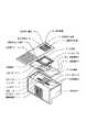
図20は、一般的な記録素子基板を示す図であり、図21は、図20に示した記録素子基板が配線基板に接続された状態を示す図である。
図20及び図21に示すように、記録素子基板1の片面には記録液を吐出するための記録素子を有する複数の吐出口2が設けられ、他方の面には吐出口2に記録液を供給するための供給口3が吐出口2列の長さとほぼ等しい長さで開口して設けられており、記録素子基板1に対して記録液を吐出するための電気パルスを印加するための配線基板4がTAB実装技術等によって接続されて記録素子ユニット6が形成される。なお、配線基板4の配線は裏面側に設けられ(不図示)ている。
また、記録素子基板1には、記録素子基板1と配線基板4とを電気的に接続するリード線(不図示)を記録液による腐食や外部から作用する力による断線から保護するために封止樹脂A5が塗布されている。
【0005】
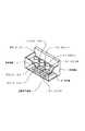
図22は、図21に示した記録素子ユニット6が設けられた従来のインクジェット記録ヘッドの一構成例を示す分解斜視図であり、図23は、図22に示したインクジェット記録ヘッドの組立完成後の外観斜視図、図24は図23に示すA−A断面の部分拡大図である。
図22及び図23に示すように、複数の記録素子ユニット6a〜6cは支持板8a〜8cを介して支持部材7の上面に接着樹脂A9a〜9c、接着樹脂B10a〜10c、接着樹脂C11a〜11cにより接着固定され、また、支持部材7の側面には、複数の配線基板4a〜4cに対する電気信号をまとめる配線統合基板12が固定されて複数の配線基板4a〜4cと電気的に接続されている。なお、20はインクの供給口である。
【0006】
そして、インクジェット記録ヘッドの記録液吐出側の面は図23に示すように、支持板8及び記録素子ユニット6の開口部と配線基板4周囲(支持板8の露出がないように)に封止樹脂B13を充填し、配線基板4裏面の配線を記録液から保護している。
また、支持板8は配線基板4を保持固定する役割の他に記録素子基板1が発生する熱を放出する放熱部材としての役割があるためアルミ等の放熱性のよい材料を使用するのが一般的となっている。そのため、支持板8も配線基板4と同様に封止樹脂B13を周囲に充填し記録液から保護する必要がある。
【0007】
【発明が解決しようとする課題】
しかしながら、上述したような従来のインクジェット記録ヘッドにおいては、封止工程を短時間で効率良く行うために、記録素子基板1の周囲と配線基板4の周囲をそれぞれ封止している。(図24封止樹脂B13a及び13b)
そのため、記録素子基板1と配線基板4の間には封止樹脂塗布機のニードルが入るだけの領域を確保する必要があり、配線基板4の外形寸法がその分大きくなる。
また、記録素子基板1は高度なフォトリソ技術により電気配線パターンが表面の外周付近まで高密度に実装されているので外周の小さなチッピングでも不良の原因となる可能性がある。したがって、記録素子ユニットの露出された電気配線部分をインクによる腐食から保護するために、充填剤をそれらの周囲に充填するに際して、この充填剤の充填を塗布機が記録素子基板に接触しないように精度良く行うことが必要となる。
また、記録素子基板1の周囲に直接封止樹脂B13を塗布するため、塗布量の制御を正確に行う必要がある。塗布量が多すぎると記録素子基板1や配線基板4の表面へ封止樹脂B13がはみ出す原因となり、封止樹脂がはみ出した状態で記録ヘッドを完成した場合、印字後に記録素子基板1の表面をクリーニングする際に障害となる可能性がある。
【0008】
また、封止樹脂B13の粘性、チキソ性の度合いによっては塗布機のニードルが封止個所から離れる際に糸引き現象を起こし、場合によっては記録素子基板1の表面に筋状に封止樹脂B13を付着させ前記同様にクリーニングの障害となる可能性がある。
また、記録素子基板1の両横をほぼ同時に封止した場合、記録素子基板1と配線基板4の接続部(封止樹脂A5の部分)の裏面には空気が残留してしまう。残留した空気の気泡は、封止樹脂B13の層を破り外側に逃げようとするか、内側に留まるかのどちらかであるが、外側に逃げた場合は封止樹脂B13の層に穴を開け封止欠陥となる。さらに気泡が破裂する際に記録素子基板1の表面に封止樹脂B13を付着させ汚してしまう可能性がある。
また、気泡が内側に留まっている場合は、記録素子基板1と配線基板4の接続部(封止樹脂A5の部分)の裏面は空洞となっており何処から記録液が配線基板4の裏面に侵入してくると配線基板4の配線を腐食する可能性がある。
【0009】
したがって、記録素子基板1と配線基板4の接続部(封止樹脂A5の部分)の裏面に気泡を残さない様な塗布方法が理想的であり、直接、記録素子基板1の周囲に封止樹脂B13を塗布する場合においては、記録素子基板1横の片側の封止個所と反対側の封止個所の塗布するタイミング、量、回数を適切に制御する必要がある。
しかし、上記記述のとおり塗布のタイミング、量、回数を適切に制御した場合には、封止工程に要する時間を大幅に拡大してしまう可能性があることを懸念しなくてはならない。
このように、従来においては、このような記録素子基板の周囲への充填剤の充填に際して、充填剤の充填を精度良く行い、充填量を適正量に制御し得るうえで、必ずしも満足の行くものがなかった。
【0010】
そこで、本発明は、上記従来のものにおける課題を解決し、記録素子基板の周囲への充填剤の充填に際して、充填剤の充填を精度良く行い、充填量を適正量に制御し得るインクジェット記録ヘッドの製造方法、インクジェット記録ヘッド、並びに該インクジェット記録ヘッドを搭載したインクジェット記録装置を提供することを目的とするものである。
また、本発明は、上記した従来の技術が有する課題を解決するため、記録素子基板の周囲に封止樹脂を充填する構造を改良して、電気及び構造的不良をなくし、また、製造工程に要する時間を短縮するとともに、ヘッド設計に自由度をもたせ、低コストで印字品質及び信頼性の高いインクジェット記録ヘッドの製造方法、インクジェット記録ヘッド、並びに該インクジェット記録ヘッドを搭載したインクジェット記録装置を提供することを目的とするものである。
【0011】
【課題を解決するための手段】
本発明は、上記課題を達成するために、つぎの(1)〜(22)のように構成したインクジェット記録ヘッドの製造方法、該製法によって製造されたインクジェット記録ヘッド及び該インクジェット記録ヘッドを搭載したインクジェット記録装置を提供するものである。
(1)インクを吐出する吐出口群を具備する記録素子基板と、記録素子基板に電気的に接続される電気配線基板と、前記記録素子基板及び前記電気配線基板を保持固定する支持部材と、を具備するインクジェット記録ヘッドの製造方法において、
前記記録素子基板と前記電気配線基板とを電気接続する電気接続部が配された領域に対して連通した充填剤溜め部に、熱硬化性充填剤を注入する工程と、
加熱することにより該充填剤溜め部に注入された熱硬化性充填剤を流動させて前記電気接続部が配された領域に充填する工程と、
前記充填された熱硬化性充填剤を硬化する工程と、
を有することを特徴とするインクジェット記録ヘッドの製造方法。
(2)前記充填剤溜め部は、前記支持部材の前記記録素子基板を支持する面の裏面側に設けられた開口部であることを特徴とする上記(1)に記載のインクジェット記録ヘッドの製造方法。
(3)前記充填剤溜め部は、前記記録素子基板を支持する前記支持部材と前記記録素子基板との段差部分であって、前記記録素子基板の電極端子が配されていない一側面に隣接した部分であることを特徴とする上記(1)に記載のインクジェット記録ヘッドの製造方法。
(4)前記記録素子基板は複数並列に設けられていることを特徴とする上記(1)乃至(3)のいずれかに記載のインクジェット記録ヘッドの製造方法。
(5)前記充填剤充填工程の加熱温度は、前記充填剤硬化工程の加熱温度よりも低いことを特徴とする上記(1)乃至(4)のいずれかに記載のインクジェット記録ヘッドの製造方法。
(6)前記充填剤充填工程の加熱温度は、前記充填剤の粘度が15ポイズ以下となる温度であることを特徴とする上記(1)乃至(5)のいずれかに記載のインクジェット記録ヘッドの製造方法。
(7)前記充填剤硬化工程の加熱温度は80℃以上であることを特徴とする上記(1)乃至(6)のいずれかに記載のインクジェット記録ヘッドの製造方法。
(8)上記(1)乃至(7)のいずれかに記載されたインクジェット記録ヘッドの製造方法によって製造されたことを特徴とするインクジェット記録ヘッド。
(9)上記(8)に記載されたインクジェット記録ヘッドを搭載するキャリッジを備えたインクジェット記録装置。
(10)インクを吐出する吐出口群を具備する記録素子基板と、記録素子基板に電気的に接続される電気配線基板と、前記記録素子基板及び前記電気配線基板を保持固定する支持部材と、を具備するインクジェット記録ヘッドにおいて、
前記記録素子基板と前記電気配線基板とを電気接続する電気接続部が配された領域に対して連通した充填剤溜め部を有していることを特徴とするインクジェット記録ヘッド。
(11)前記充填剤溜め部は、前記支持部材の前記記録素子基板を支持する面の裏面側に設けられた開口部であり、前記記録素子基板の側面に隣接した領域に連通していることを特徴とする上記(10)に記載のインクジェット記録ヘッド。
(12)前記充填剤溜め部から前記記録素子基板の周囲に封止樹脂が充填されていることを特徴とする上記(10)に記載のインクジェット記録ヘッド。
(13)前記充填剤溜め部が、前記記録素子基板と前記配線基板を電気的に接続する部分の裏面側中央付近に向けて設けられていることを特徴とする上記(10)乃至(12)のいずれかに記載のインクジェット記録ヘッド。
(14)前記充填剤溜め部が、前記記録素子基板側に向けて先細りした形状に形成されていることを特徴とする上記(10)乃至(13)のいずれかに記載のインクジェット記録ヘッド。
(15)前記充填剤溜め部が、前記記録素子基板の片側の封止箇所および該箇所と反対側の封止箇所にそれぞれ位置するように設けられていることを特徴とする上記(10)に記載のインクジェット記録ヘッド。
(16)前記支持部材は、前記記録素子基板が前記支持部材と接するための開口部を有し、前記配線基板と前記支持部材との間に介在することにより、前記配線基板を保持固定する支持板と、前記記録素子基板と前記支持部材との間に介在することにより、前記記録素子基板を保持固定する支持基板と、を有していることを特徴とする上記(10)乃至(15)のいずれかに記載のインクジェット記録ヘッド。
(17)前記支持基板に、前記支持部材の裏面に設けられた前記充填剤溜め部から、前記記録素子基板と前記支持板との間に連通する連通孔が設けられていることを特徴とする上記(16)に記載のインクジェット記録ヘッド。
(18)先細りした形状に形成されている前記充填剤溜め部の先端部の穴径は、支持基板に設けられた前記連通孔の穴径と、ほぼ同径とされていることを特徴とする上記(17)に記載のインクジェット記録ヘッド。
(19)前記支持基板には、前記充填剤溜め部に連通する複数の前記連通孔が設けられていることを特徴とする上記(17)に記載のインクジェット記録ヘッド。
(20)前記支持基板に設けられた前記連通孔自体が、充填剤溜め部となっていることを特徴とする上記(16)乃至(19)のいずれかに記載のインクジェット記録ヘッド。
(21)前記充填剤溜め部は、前記記録素子基板を支持する前記支持部材と前記記録素子基板との段差部分であって、前記記録素子基板の電極端子が配されていない一側面に隣接した部分であることを特徴とする上記(10)に記載のインクジェット記録ヘッド。
(22)上記(10)に記載されたインクジェット記録ヘッドを搭載するキャリッジを備えたインクジェット記録装置。
【0012】
【発明の実施の形態】
上記構成を用いた本発明の実施の形態においては、記録素子基板の周囲に直接、封止樹脂を塗布しないため、記録素子基板と配線基板の間に封止樹脂塗布機のニードルが入るだけの領域を確保する必要がなくなり、配線基板の外形寸法をその分小さくすることができる。
また、記録素子基板の周囲、特に電極部分に直接、封止樹脂を塗布しないため、塗布量の急激な変化が少なく、塗布量制御が容易になる。
また、記録素子基板の周囲に直接、封止樹脂を塗布しないため、塗布機のニードルが封止個所から離れる際に封止樹脂が糸引き現象を起こさなくなり、記録素子基板表面への付着を防止できる。
また、記録素子基板の周囲に直接、封止樹脂塗布機のニードルを近づけることがなくなるため、記録素子基板の外周にチッピングを発生させる可能性がなくなる。
また、記録素子基板横の片側の封止剤塗布個所と反対側の封止剤塗布個所の封止樹脂を塗布するタイミングを制御する必要がないように構成することができ、封止工程に要する時間を短縮できる。
また、充填剤溜め部を、記録素子基板と配線基板を電気的に接続する部分の裏面側中央付近に連通して設けることにより、封止樹脂をその部分から充填するようにでき、気泡の残留を防止できる。
また、充填剤溜め部を先細りした形状とすることにより、封止樹脂を注入する側の口を広げることができ、封止樹脂塗布機の位置制御が容易になる。
また、記録素子基板と前記支持部材との間に支持基板を介在させるようにし、支持部材に設けた充填剤溜め部を先細りした形状とし、その先細り先端部と、支持基板に設けられた連通孔との穴径差が減少するように構成することにより、封止樹脂を充填する際にその部分に封止樹脂が残留しにくくすることができ、必要な封止樹脂量を減らすことができる。
また、記録素子基板と前記支持部材との間に支持基板を介在させ、前記支持基板に、充填剤溜め部から記録素子基板に連通する複数の連通孔を設けることにより、一度の塗布で複数の連通孔から充填することが可能となり、工程時間を短縮することができる。
以上により、電気及び構造的な不良がなく、しかも、低コストで印字品質及び信頼性の高いインクジェット記録ヘッドを提供することができる。
【0013】
【実施例】
以下に、本発明の実施例について説明する。
[実施例1]
図1は、本発明の実施例1における記録ヘッドの部分拡大図であり、図2は、図1に示す記録ヘッドに用いる記録素子基板の一例を説明する図である。
また、図3は、図1に示す記録ヘッドの分解斜視図であり、図4は、図1に示す記録ヘッドの記録素子ユニットとタンクホルダーユニットの結合を説明する図である。そして、図5は、図1に示す記録ヘッドの全体図である。
本実施例の記録ヘッド1001は、電気信号に応じて膜沸騰をインクに対して生じせしめるための熱エネルギーを生成する電気熱変換体を用いて記録を行うバブルジェット方式のサイドシュータ型とされる記録ヘッドである。
【0014】
記録ヘッド1001は、図4に示すように、記録素子ユニット1002とタンクホルダーユニット1003から構成され、この記録素子ユニット1002は、並列に配置された記録素子基板間の隙間に連通する充填剤溜め部1311を有し、この充填剤溜め部に溜めた熱硬化性充填剤を加熱することにより記録素子基板周囲に充填して、電気接続部分をインクによる腐食や外的衝撃から保護するように構成されている。
また、図3の分解斜視図に示すように、記録素子ユニット1002は、記録素子基板1100、第1のプレー卜1200、電気配線基板1300、第2のプレート1400で構成されており、また、タンクホルダーユニット1003は、タンクホルダー1500、流路形成部材1600、フィルター1700、シールゴム1800から構成されている。
【0015】
上記のように構成された記録ヘッドについて、これらの構成を簡単に説明しながら、全体を説明することにする。
まず、本実施例における記録素子ユニットについて説明する。
図2は、記録素子基板1100の構成を説明するために一部分解した斜視図である。
記録素子基板1100は、例えば、厚さ0.5〜1mmのSi基板1101で薄膜が形成されている。
また、2色のインク流路として長溝状の貫通口からなるインク供給口1102が2つ形成され、各々のインク供給口1102の両側に電気熱変換素子1103がそれぞれ1列ずつ千鳥状に配列されており、前記電気熱変換素子1103と、電気熱変換素子1103に電力を供給するAl等の電気配線は成膜技術により形成されている。
また、前記電気配線に電力を供給するための電極部1104には、パターニングによるメッキやワイヤボンディングによるボール電極形成(スタッドバンプ)によりAu等のバンプ1105が設けられている。
【0016】
前記インク供給口1102は、前記Si基板1101の結晶方位を利用した異方性エッチングにより形成される。ウエハー面に<100>、厚さ方向に<111>の結晶方位を持つ場合、アルカリ系(KOH、TMAH、ヒトラジン等)の異方性エッチングにより、約54.7度の角度でエッチングが進行する。この方法を用いて、所望の深さにエッチングする。
また、前記Si基板1101上には、電気熱変換素子1103が具備される発泡室1109に連通するインク流路を形成するためのインク流路壁1106と吐出口1107がフォトリソ技術により形成され、2色のインクに対応した2列の吐出口群1108を形成している。
また、前記吐出口1107に対向するように前記電気熱変換素子1103は設けられており、インク供給口1102から供給されたインクを膜沸騰の作用により吐出させるものである。
【0017】
本実施例おいては、図1及び図3に示すように3つの記録素子基板1100a、1100b、1100cにより、6色のインク(ブラック:Bk、ライトシアン:LC、ライトマゼンタ:LM、シアン:C、マゼンタ:M、イエロー:Y)に対応する6つの吐出口群1108Bk、1108LC、1108LM、1108C、1108M、1108Yを具備している。
そして、図3に示す第1のプレート1200は、例えば、厚さ0.5〜10mmのアルミナ(Al2O3)材料で形成されている。なお、第1のプレート1200の素材は、アルミナに限られることなく、記録素子基板1100の材料の線膨張率と同等の線膨張率を有し、かつ、記録素子基板1100材料の熱伝導率と同等もしくは同等以上の熱伝導率を有する材料で作られてもよい。
【0018】
第1のプレート1200の素材は、例えば、シリコン(Si)、窒化アルミニウム(AlN)、ジルコニア、窒化珪素(Si3N4)、炭化珪素(SiC)、モリブデン(Mo)、タングステン(W)のうちいずれであってもよい。
第1のプレート1200には、記録素子基板1100に6色のインクを供給するための6つのインク供給口1201が等ピッチで形成されており、3つの記録素子基板1100a、1100b、1100cに2つづつ形成された6つのインク供給口1102が第1のプレー卜1200の6つのインク供給口1201にそれぞれ対応し、かつ、図1に示すように3つの記録素子基板1100a、1100b、1100cに2つづつ形成された6つの吐出口群1108Bk、1108LC、1108LM、1108C、1108M、1108YのそれぞれのピッチPa、Pb、Pc、Pd、Peが全て等しくなるように位置精度良く第1のプレート1200に接着固定されている。
【0019】
接着に用いられる第1の接着剤1202は第1のプレート1200上に略記録素子基板形状で、しかも、隣り合うインク供給口間にエアーパスが発生しないように塗布されている。
その第1の接着剤1202は、例えば、粘度が低く、接触面に形成される接着層が薄く、かつ、硬化後、比較的高い硬度を有し、かつ、耐インク性のあるものが望ましい。
その第1の接着剤1202は、例えば、エポキシ樹脂を主成分とした熱硬化接着剤であり、接着層の厚みは50μm以下が望ましい。
【0020】
電気配線基板1300は、記録素子基板1100に対してインクを吐出するための電気信号を印加するものであり、記録素子基板1100を組み込むための開口部と、記録素子基板1100の電極1104に対応する電極端子(不図示)と、この配線端部に位置し本体装置からの電気信号を受け取るための外部信号入力端子1301を有している。
電気配線基板1300と記録素子基板1100は、電気的に接続されており、接続方法は、例えば、記録素子基板1100の電極1104と電気配線基板1300の電極端子間に熱硬化接着樹脂(不図示)を塗布後、前記記録素子基板1100の電極1104と前記電気配線基板1300の電極端子をヒートツールにて一括で加熱加圧して、熱硬化接着樹脂を硬化させることにより、該電極1104と該電極端子は電気的に一括接続される。また、熱硬化接着樹脂としては、導電粒子を含んだ異方性導電接着剤を用いた場合も、同様に可能である。
【0021】
本実施例の構成において、例えば、ニッケルの単粒子径が2〜6μmの導電粒子とエポキシ樹脂を主成分とする接着剤で構成される異方性導電接着膜を用いて、記録素子基板1100の電極1104と電気配線基板1300の金メッキされた電極端子部を、温度170〜250℃で加熱圧着したところ、好適に電気接続された。
電気配線基板1300の素材としては、例えば、配線が二層構造のフレキシブル配線基板が使用され、表層はレジストフィルムで覆われている。
また、外部信号入力端子1301の裏面側には、補強板1303が接着され、外部信号入力端子1301部の平面性を向上させている。補強板1303の素材としては、例えば0.5〜2mmのガラエポ、アルミ等の耐熱性のある材料が使用される。
【0022】
第2のプレート1400は、例えば、厚さ0.5〜1mmのアルミナ(Al2O3)材料で形成されている。なお、第2のプレートの素材は、アルミナに限られることなく、記録素子基板1100及び第1のプレート1200と同等の線膨張率を有し、かつ、それらの熱伝導率と同等もしくは同等以上の熱伝導率を有する材料で作られてもよい。そして、第2のプレート1400は、第1のプレート1200に接着固定された記録素子基板1100の外形寸法よりも大きな開口部を有する形状となっている。
また、記録素子基板1100と電気配線基板1300を平面的に電気接続できるように第1のプレート1200に第2の接着剤1203により接着されており、電気配線基板1300の裏面が第3の接着剤1306により接着固定されている。
また、電気配線基板1300は、第2のプレート1400に接着されると同時に、図3に示すように第1のプレート1200及び第2のプレート1400の一側面で折り曲げられ、第1のプレート1200の側面に第3の接着剤1306で接着されている。第2の接着剤1203は、例えば、粘度が低く、接触面に形成される接着層が薄く、かつ、耐インク性のあるものが使用される。また、第3の接着剤1306は、例えば、エポキシ樹脂を主成分とした厚さ10〜100μmの熱硬化接着膜が使用される。
【0023】
以上のように構成された記録素子ユニット1002の記録素子基板1100と電気配線基板1300の電気接続部分は、第1の充填剤及び第2の充填剤により充填されており、電気接続部分をインクによる腐食や外的衝撃から保護している。
記録素子基板1100周辺の構造としては、図3に示すように第2のプレート1400が第1のプレート1200上にダムを形成するように接着固定され、かつ、そのダム内に記録素子基板1100が接着固定される。
そのようにして組み合わされた部材の概略構成の部分平面図を図16(A)に、図16(A)内のA−A断面図を図16(B)、B−B断面図を図16(C)として示す。
図16に示される通り、第1のプレート1200上に第2のプレート1400が積層され、その上方に記録素子基板1100が積層され、記録素子基板1100を露出させる開口が形成され、該開口端部の裏面に電気配線1314(図16(A)では電気配線1314が理解し易いように電気配線基板1300の表面に存在するように図示したが、実際は前述の通り裏面に配されているものである。)が形成された電気配線基板1300がさらに積層される。ここで、電気配線基板1300に設けられた端子1314は、記録素子基板1100に設けられた電極1104に対応して配置されており、記録素子基板1100に対して電気配線基板1300を積層する際に位置合わせが行われる。
この状態では、図16(B)、(C)に示される通り、充填剤溜め部1311及び、後に充填剤(1312)が充填される隙間領域1315は空間部分とされている。そして、充填剤溜め部1311は隙間領域1315に充填剤を充填するための充填剤注入口となっている。
このように積層形成された記録素子ユニット1002は、後述する製造装置のワーク固定ステージに1704に載置され、充填剤が充填される。
本例において使用される充填剤は、2種類あり、充填剤溜め部1311から充填され、隙間領域1315に充填される第1の充填剤1312と、電気配線基板1300の電気配線1314と記録素子基板1100の電極1104との接続を確保し、電気配線1314が露出する先端部分を封止する第2の充填剤1308とである。
本例で使用される第1の充填剤1312は、例えば、記録素子間の隙間を30〜300μmと設定しているため、ベアチップ実装に用いるフリップチップ用アンダーフィル剤等の浸透性の良い充填剤を用いており、具体的には、エポキシ樹脂を主成分とするフリップチップ用アンダーフィル剤である。第1の充填剤1312は熱硬化充填剤(フリップチップ用アンダーフィル剤)は、粘度が常温でおよそ50ポイズであるが、40〜70℃に加熱することにより15ポイズ以下まで低下する特性を有するものである。そのため、充填剤を充填する際には、製造装置に載置された記録素子ユニット1002の第1のプレート1200を40〜70℃に加熱しながら、第1の充填剤1312を充填剤溜め部1311に適量充填した後、記録素子基板周囲に全域にアンダーフィル剤が浸透するまで約3〜10分程度放置する。なお、図6に本実施例で使用した熱硬化充填剤の粘度特性を示す。
また、第2の充填剤1308は、アンダーフィル剤とほぼ同成分ではあるが高粘度で流動性の低いものが使用される。
以下、簡単に製法を順を追って説明する。
上述したように積層組み立てされた記録素子ユニット1002は、ワーク固定ステージ1704に固定される。そして、この記録素子ユニットに対する充填剤の充填は、図19に示される製造装置の移動アームA1701、移動アームB1702、移動アームC1703が夫々、X軸方向、Y軸方向、Z軸方向に移動しながら位置決めがなされ、充填剤容器A1705内から加圧装置1708によって加圧供給されたエアによって押出された第1の充填剤1312が図17(A)及び(B)に示すように充填剤溜め部1311に充填される。この時、図18(C)に示される通り、記録素子基板間の隙間に対しても第1の充填剤1312は流動して回り込み充填される。
なお、第1の充填剤1312の充填工程では、ワークである記録素子ユニット1002を搭載したワーク固定ステージ1704は温度調節され、第1プレート1200が40℃〜70℃に温調されている。そのため、第1の充填剤1312は、粘度が低下し、3〜10分放置することによって、充填剤溜め部1311から隙間領域1315へと流動し、図18(A)、(B)に示される通り、充填剤溜め部1311に第1の充填剤1312がほとんど残存することなく、隙間領域1315内へ移動し第1の充填剤1312によって満たされた状態となる。
その後、ほぼ同成分ではあるが高粘度で流動性の低い第2の充填剤1308を、記録素子基板1100表面に位置する電気配線基板1300の開口部の電気配線部1314が露出しないように塗布し配線の接続を確保する。
以上の製造装置における各種の制御は、符号1709で示される制御装置によって行われるものである。
第1の充填剤1312、第2の充填剤1308の充填が終了したところで、ワークである記録素子ユニット1002は、ステージ1704から取外された後、オーブンに入れられ、2種類の充填剤を同時に80〜150℃で2〜5時間の熱硬化を行っている。
ここで、使用する第1の充填剤の充填量の目安としては、電気配線基板1300裏面の電気配線が完全に充填される量であるが、記録素子基板1100は構造的にインク供給口1102の長手方向に対して垂直に作用する外力、つまり、充填剤溜め部1311が設けられている方向に作用する外力に弱いため、熱硬化後の状態で充填剤溜め部1311に残留する第1の充填剤の量が少ないほど良い。
【0024】
本実施例においては、残留する第1の充填剤の厚みを記録素子基板1100の厚みの1/3以下程度にすることによって、好適な充填状態を得ることができた。また、第2の充填剤1308の塗布量に関しては、充填剤高さが、記録素子基板1100の吐出口面と記録紙の間隔を左右し、さらには、印字品位に影響を与えるため、高さを低く抑えるほど良い。
以上のように構成された記録素子ユニット1002の電気配線基板1300は、ホルダーユニット1003の形状に合わせて、さらに、フォーミングされる。
【0025】
つぎに、タンクホルダーユニットについて説明する。
図3に示すタンクホルダー1500は、例えば、樹脂成形により形成される。該樹脂材料には、形状的剛性を向上させるためにガラスフィラーを5〜40%混入した樹脂材料を使用することが望ましい。
タンクホルダー1500は、着脱自在のインクタンクを保持するものである。
また、インクタンクから記録素子ユニット1002にインクを導くためのインク流路1501を形成するタンクホルダーユニット1003の一構成部品であり、流路形成部材1600を超音波溶着することによりインク流路1501を形成している。
また、インクタンクと係合するジョイント(不図示)には、外部からのゴミの進入を防ぐためのフィルター1700が熱溶着により接合されており、さらに、ジョイント部からのインクの蒸発を防止するために、シールゴム1800が装着されている。
【0026】
つぎに、記録ヘッドユニットとタンクホルダーユニットとを結合する構成について説明する。
先述の図4に示した通り、記録ヘッド1001は、記録ヘッドユニット1002とタンクホルダーユニット1003の結合により構成されている。構成は以下の通りである。
記録素子ユニット1002のインク供給口(第1のプレート1200のインク供給口1201)とタンクホルダーユニット1003のインク供給口(流路形成部材1600のインク供給口1601)を連通させるように第4の接着剤1602が塗布され、接着固定されている。
また、インク供給口部分以外にも記録素子ユニット1002とタンクホルダーユニット1003の接する部分を数ヶ所、第5の接着剤1603で接着固定している。第4の接着剤1602と第5の接着剤1603は、耐インク性があり、かつ、常温で硬化し、かつ、異種材料間の線膨張差に耐えられる柔軟性のある接着剤が望ましく、本実施例においては、例えば、吸湿硬化型のシリコーン接着剤を使用している。
【0027】
また、第4の接着樹脂1602と第5の接着樹脂1603は、同一の接着剤でも構わない。また、記録素子ユニット1002をタンクホルダーユニット1003に第4の接着剤1602と第5の接着剤1603で接着する際に、記録素子ユニット1002を第6の接着剤1604で位置決め固定している。該第6の接着剤1604は、瞬時に硬化する接着剤が望ましく、本実施例においては、例えば、紫外線硬化接着剤を使用しているが、他の接着剤でも構わない。
また、記録素子ユニット1002の外部信号入力端子1301部分はタンクホルダー1500の一側面に、端子位置決めピン1515(2ヶ所)と端子位置決め穴1309(2ヶ所)により位置決めし、固定されている。固定方法は、例えば、タンクホルダー1500に設けられた端子結合ピン1515と、電気配線基板1300の外部信号入力端子1301周辺に設けられた端子結合穴1310をはめ合い、端子結合ピン1515を熱溶着することにより固定しているが、その他の固定手段を用いても良い。
以上の構成よりなる本実施例のインクジェット記録ヘッドは、充填剤溜め部に溜めた熱硬化性充填剤を過熱することにより記録素子基板周囲に充填剤を充填するため、隣り合う記録素子基板間を直接塗布することがなくなるため、記録素子基板間の隙間が30μmほどの狭いギヤップの場合においても良好な充填が可能となり、電気配線基板のサイズを小型化することができる。また、充填剤溜め部に隣接する個所以外は、充填剤の塗布機が記録素子基板に接触する可能性がなくなる。
従って、コンパクトで、電気的信頼性の高い、インクジェット記録ヘッドを提供することができる。
【0028】
[実施例2]
図7、図8、図9は、本発明のインクジェット記録ヘッドの実施例2の構成を示す図であり、図7は分解斜視図、図8は組立完成後の外観斜視図、図9はヘッドの裏面及び内部の構造を説明する図である。
本実施例の記録ヘッドは、図7、図8、図9に示すように、記録液を吐出するための記録素子を有する吐出口2がそれぞれ複数配列された複数の記録素子基板1a〜1cと、記録素子基板1a〜1cが組み込まれるための開口部を有している。
そして、TAB実装等によって、前記開口部に組み込まれた記録素子基板1a〜1cのそれぞれと接続されている。
この記録ヘッドは、記録素子基板1a〜1cのそれぞれに対して記録液を吐出させるための電気信号を送る配線基板4a〜4cと、記録素子基板1a〜1cと配線基板4a〜4cとをそれぞれ接続するリード線を記録液による腐食や外部から作用する力による断線から保護するための封止樹脂A5と、記録素子基板1a〜1cを接着樹脂A9a〜9cにより接着固定するための支持部材7と、記録素子基板1a〜1cが支持部材7と接するための開口部を有しており、配線基板4a〜4cを接着樹脂C11a〜11cにより接着固定するための支持板8a〜8cと、支持板8a〜8cを支持部材7に保持固定する接着樹脂B10a〜10cと、配線基板4a〜4cに対する電気信号をまとめる配線統合基板12とから構成されている。
なお、支持部材7は封止樹脂B13を裏面側から記録素子基板1a〜1c周囲に充填するための注入口A16を具備している。
【0029】
以下に、上記のように構成されたインクジェット記録ヘッドの組立方法について説明する。
まず、シリコンウェハー上に発熱抵抗層及び配線などをフォトリソグラフィー技術によってパターニングし、次に、ノズル壁及び吐出口2を感光性樹脂によって形成し、次に、異方性エッチング、サンドブラスト等によって記録液供給口A3を形成し、その後、切断によって外形を形成することにより、記録素子基板1a〜1cを形成する。
次に、記録素子基板1a〜1cをそれぞれ、電気信号を受け取るための配線基板4a〜4cとTAB実装技術等によって電気的に接続し、接続に使用される記録素子基板1a〜1c側の電気信号入力端子と配線基板4a〜4c側のリード線上に封止樹脂A5を塗布する。
【0030】
次に、放熱性の良いアルミ等の材料を用いプレス加工、切削加工により外形及び開口部を形成した支持板8a〜8cを接着樹脂B10a〜10cにより支持部材7に接着固定する。
次に、記録素子基板1a〜1cを、それぞれ接着樹脂A9a〜9cによって支持部材7に接着固定し、また、配線基板4a〜4cを、それぞれ接着樹脂C11a〜11cによって支持板8a〜8cに接着固定することにより、記録素子基板1a〜1cと配線基板4a〜4cとからなる記録素子ユニット6a〜6cを、支持部材7と支持板8a〜8cからなるインクジェット記録ヘッドの構造体に固定することができる。
そして、配線基板4a〜4cと配線統合基板12とを電気的に接続し、配線統合基板12を接着、熱加締め等の方法により、支持部材7に保持固定する。
その後、支持部材7に設けた注入口A16a〜16fを用い、支持部材7の裏面側より記録素子基板1a〜1cの周囲に封止樹脂B13を充填する。
注入口A16a〜16fに充填された封止樹脂は、実施例1で説明した充填剤と同様の特性を具えるものであって、注入口ヘの充填が終了した後、加熱(およそ40−70℃)し流動(3−10分程度放置)させて記録素子基板の周囲へと充填する。
その後、封止樹脂を流動させた温度より高い温度(およそ80−150℃)に加熱し、2−5時間かけて封止樹脂を熱硬化する。
なお、注入口A16a〜16fは記録素子基板1a〜1cと支持板8a〜8cの間で、しかも記録素子基板1と配線基板4を電気的に接続する部分の裏面側中央付近に向けて設けている。
【0031】
また、注入口A16a〜16fは記録素子基板側に向けて先細りしている。
従って本形態においては、記録素子基板1a〜1cの周囲に直接、封止樹脂B13を塗布しないため、記録素子基板1a〜1cと配線基板4a〜4cの間に封止樹脂塗布機のニードルが入るだけの領域を確保する必要がなくなり、配線基板4の外形寸法をその分小さくできる。
また、記録素子基板1a〜1cの周囲に直接、封止樹脂B13を塗布しないため、塗布量の急激な変化が少なく、塗布量制御が容易になる。
また、記録素子基板1a〜1cの周囲に直接、封止樹脂B13を塗布しないため、塗布機のニードルが封止個所から離れる際に封止樹脂B13が糸引き現象を起こさなくなり、記録素子基板1表面への付着を防止できる。
また、記録素子基板1a〜1cの周囲に直接、封止樹脂B13の塗布機のニードルを近づけることがなくなるため、記録素子基板1a〜1cの外周にチッピングを発生させる可能性がなくなる。
また、記録素子基板1a〜1c横の片側の封止剤塗布個所と反対側の封止剤塗布個所の封止樹脂B13を塗布するタイミングを制御する必要がなくなり、封止工程に要する時間を短縮できる。
また、注入口A16a〜16fは、記録素子基板1a〜1cと配線基板4a〜4cを電気的に接続する部分の裏面側中央付近に向けて設けられているため、封止樹脂B13はその部分から充填されていき、気泡の残留を防止できる。
また、注入口A16a〜16fを先細りした形状とするため、封止樹脂B13を注入する側の口を広げることができ、封止樹脂B13の塗布機の位置制御が容易になる。
【0032】
[実施例3]
図10、図11、図12は、本発明のインクジェット記録ヘッドの実施例3の構成を示す図であり、図10は分解斜視図、図11は組立完成後の外観斜視図、図12はヘッドの裏面及び内部の構造を説明する図である。
本形態は図10に示すように、複数の吐出口列を持つ記録素子基板1と配線基板4からなる記録素子ユニット6と支持板8と支持基板14と支持部材7からなるインクジェット記録ヘッドである。
近年、インクジェット記録ヘッドは写真画質を実現するための多色化が進み、1つのヘッドに複数の記録素子基板が搭載されるのが一般的となってきた。また、高品位な画像を出力するためにも前述の複数の記録素子基板を一体化し、フォトリソ技術のパターニング精度で配列した記録素子基板1を配線基板4に電気的に接続している。
【0033】
また、本実施例においては各色の吐出口列が非常に接近しているため、支持部材7に設けられた各記録液の流路18の中央付近に集合するようになっている。また、前記流路18は支持部材7に設けられた溝周囲に接着樹脂D15を塗布し支持基板14を接着することにより形成している。
そして、封止樹脂B13は支持部材7の裏面側より塗布され、注入口A16a,16bと注入口B17a,17bを介して記録素子基板1周囲に充填される。
注入口A16a、16b、注入口B17a、17bに充填された封止樹脂は、実施例1で説明した充填剤と同様の特性を具えるものであって、注入口ヘの充填が終了した後、加熱(およそ40−70℃)し流動(3−10分程度放置)させて記録素子基板の周囲へと充填する。
その後、封止樹脂を流動させた温度より高い温度(およそ80−150℃)に加熱し、2−5時間かけて封止樹脂を熱硬化する。
注入口A16a,16bに関しては、記録素子基板側に向かって先細りした形状とし、注入口B17a,17bとの接続側の穴径を注入口B17a,17bとほぼ同程度にしている。
注入口B17a,17bに関しては、記録素子基板1と配線基板4を電気的に接続する部分の裏面側中央付近に向けて設けている。
従って、本実施例においては、記録素子基板1の周囲に直接、封止樹脂B13を塗布しないため、記録素子基板1と配線基板4の間に封止樹脂塗布機のニードルが入るだけの領域を確保する必要がなくなり、配線基板4の外形寸法をその分小さくできる。
【0034】
また、記録素子基板1の周囲に直接、封止樹脂B13を塗布しないため、塗布量の急激な変化が少なく、塗布量制御が容易になる。
また、記録素子基板1の周囲に直接、封止樹脂B13を塗布しないため、塗布機のニードルが封止個所から離れる際に封止樹脂B13が糸引き現象を起こさなくなり、記録素子基板1表面への付着を防止できる。
また、記録素子基板1の周囲に直接、封止樹脂B13の塗布機のニードルを近づけることがなくなるため、記録素子基板1の外周にチッピングを発生させる可能性がなくなる。
また、記録素子基板1横の片側の封止剤塗布個所と反対側の封止剤塗布個所の封止樹脂B13を塗布するタイミングを制御する必要がなくなり、封止工程に要する時間を短縮できる。
また、注入口A16a,16b及び注入口B17a,17bは、記録素子基板1と配線基板4を電気的に接続する部分の裏面側中央付近に向けて設けているため、封止樹脂B13はその部分から充填されていき、気泡の残留を防止できる。
また、注入口A16a,16bを先細りした形状とするため、封止樹脂B13を注入する側の口を広げることができ、封止樹脂B13の塗布機の位置制御が容易になる。また、注入口B17a,17bとの接続側の穴径を注入口B17a,17bと同程度にしているため注入口A16a,16bと注入口B17a,17bの段差が減少し、そこに封止樹脂B13が残留しにくくなる。
【0035】
[実施例4]
図13、図14、図15は、本発明のインクジェット記録ヘッドの実施例の構成を示す図であり、図13は分解斜視図、図14は組立完成後の外観斜視図、図15はヘッドの裏面及び内部の構造を説明する図である。
本形態は図13に示すように、複数の記録素子基板1a〜1cと配線基板4からなる記録素子ユニット6と支持板8と支持基板14と支持部材7からなるインクジェット記録ヘッドである。
インクジェット記録ヘッドを低コスト化するには、コストの大半を占める記録素子基板を小チップ化し、1ウェハー当たりの取り個数を増やすのが効果的であり、また、記録素子基板を各色ごとに細分化することにより、歩留まりの向上をはかることができる。従って、複数の記録素子基板1a〜1cを配線基板4に電気的に接続して1つの記録素子ユニットとしている。
【0036】
そして、各記録素子基板1a〜1cと配線基板4の電気的接合部分の裏面側にそれぞれ注入口B17a〜17fを具備しており、支持部材7に設けた注入口A16a,16bから封止樹脂B13を充填している。
注入口A16a、16bに充填された封止樹脂は、実施例1で説明した充填剤と同様の特性を具えるものであって、注入口ヘの充填が終了した後、加熱(およそ40−70℃)し流動(3−10分程度放置)させて記録素子基板の周囲へと充填する。
その後、封止樹脂を流動させた温度より高い温度(およそ80−150℃)に加熱し、2−5時間かけて封止樹脂を熱硬化する。
注入口B17a〜17fは、記録素子基板1と配線基板4を電気的に接続する部分の裏面側中央付近に向けて設けられ、また、注入口A16a,16bは配線基板4との同一接続側の注入口B17a,17c,17eもしくは17b,17d,17fに対応しているため一度の塗布で複数の注入口B17a〜17fから封止樹脂B13を記録素子基板1a〜1cの周囲へ充填することが可能になっている。
従って、本実施例においては、記録素子基板1a〜1cの周囲に直接、封止樹脂B13を塗布しないため、記録素子基板1a〜1cと配線基板4の間及び隣り合う記録素子基板1a〜1c間に封止樹脂塗布機のニードルが入るだけの領域を確保する必要がなくなり、配線基板4の外形寸法をその分小さくできる。
【0037】
また、記録素子基板1a〜1cの周囲に直接、封止樹脂B13を塗布しないため、塗布量の急激な変化が少なく、塗布量制御が容易になる。
また、記録素子基板1a〜1cの周囲に直接、封止樹脂B13を塗布しないため、塗布機のニードルが封止個所から離れる際に封止樹脂B13が糸引き現象を起こさなくなり、記録素子基板1a〜1c表面への付着を防止できる。
また、記録素子基板1a〜1cの周囲に直接、封止樹脂B13の塗布機のニードルを近づけることがなくなるため、記録素子基板1a〜1cの外周にチッピングを発生させる可能性がなくなる。
また、記録素子基板1a〜1c横の片側の封止個所と反対側の封止個所の封止樹脂B13を塗布するタイミングを制御する必要がなくなり、封止工程に要する時間を短縮できる。
また、注入口A16a,16b及び注入口B17a〜17fは、記録素子基板1a〜1cと配線基板4を電気的に接続する部分の裏面側中央付近に向けて設けられているため、封止樹脂B13はその部分から充填されていき、気泡の残留を防止できる。
また、注入口A16a,16bは配線基板4との同一接続側の注入口B17a,17c,17eもしくは17b,17d,17fに対応しているため一度の塗布で複数の注入口B17a〜17fから封止樹脂B13を記録素子基板1a〜1cの周囲へ充填することが可能になり、製造工程を短縮できる。
【0038】
【発明の効果】
以上説明したように、本発明によると、記録素子基板の周囲への充填剤の充填に際して、充填剤の充填を良好に行うことができ、充填量を適正量に制御することが可能となる。
本発明は、以上に説明したように構成されているので、電気及び構造的不良をなくし、コンパクトで信頼性の高いインクジェット記録ヘッドを実現することができる。
また、本発明によると、封止を必要とするエリア(封止領域)に連通する充填剤溜め部を設け、該充填剤溜め部から封止領域に封止樹脂を充填するため、封止領域となる記録素子基板の周囲には、及び隣り合う記録素子基板間に封止樹脂塗布機のニードルが入るだけの領域を確保する必要がなくなり、配線基板の外形寸法をその分小さくすることが可能となる。
また、本発明によると、記録素子基板の周囲に直接、封止樹脂を塗布しないため、塗布量の急激な変化が少なく、塗布量制御が容易になる。
また、本発明によると、記録素子基板の周囲に直接、封止樹脂を塗布しないため、塗布機のニードルが封止個所から離れる際に封止樹脂が糸引き現象を起こさなくなり、記録素子基板表面への付着を防止できる。
また、本発明によると、記録素子基板の周囲に直接、封止樹脂塗布機のニードルを近づけることがなくなるため、記録素子基板の外周にチッピングを発生させる可能性がなくなる。
また、本発明によると、記録素子基板横の片側の封止剤塗布個所と反対側の封止剤塗布個所の封止樹脂を塗布するタイミングを制御する必要をなくすことができ、封止工程に要する時間を短縮できる。
また、本発明によると、充填剤溜め部を、記録素子基板と配線基板を電気的に接続する部分の裏面側中央付近に連通するように設けることにより、封止樹脂はその部分から充填することができ、気泡の残留を防止できる。
また、本発明によると、充填剤溜め部を先細りした形状とすることにより、封止樹脂を注入する側の口を広げることができ、封止樹脂塗布機の位置制御が容易になる。
また、本発明によると、記録素子基板と前記支持部材との間に支持基板を介在させ、充填剤溜め部を先細りした形状とし、その先細り先端部と、支持基板に設けられた連通孔との穴径差が減少するように構成することにより、封止樹脂を充填する際にその部分に封止樹脂が残留しにくくすることができ、必要な封止樹脂量を減らすことができる。
また、記録素子基板と前記支持部材との間に支持基板を介在させ、前記支持基板に、充填剤溜め部から封止領域に連通する複数の連通孔を設けることにより、一度の塗布で複数の連通孔から充填することが可能となり、工程時間を短縮させることができる。
【図面の簡単な説明】
【図1】本発明の実施例1における記録ヘッドの構成を示す部分拡大図である。
【図2】図1に示す記録ヘッドに用いる記録素子基板を説明する図である。
【図3】図1に示す記録ヘッドの分解斜視図である。
【図4】図1に示す記録ヘッドの記録素子ユニットとタンクホルダーユニットの結合を説明する図である。
【図5】図1に示す記録ヘッドの全体図である。
【図6】本実施例における熱硬化充填剤の粘度特性を説明する図である。
【図7】本発明のインクジェット記録ヘッドの実施例2の構成を示す分解斜視図である。
【図8】本発明のインクジェット記録ヘッドの実施例2の構成を示す組立完成後の外観斜視図である。
【図9】本発明のインクジェット記録ヘッドの実施例2の構成を示すヘッドの裏面及び内部の構造図である。
【図10】本発明のインクジェット記録ヘッドの実施例3の構成を示す分解斜視図である。
【図11】本発明のインクジェット記録ヘッドの実施例3の構成を示す組立完成後の外観斜視図である。
【図12】本発明のインクジェット記録ヘッドの実施例3の構成を示すヘッドの裏面及び内部の構造図である。
【図13】本発明のインクジェット記録ヘッドの実施例4の構成を示す分解斜視図である。
【図14】本発明のインクジェット記録ヘッドの実施例4の構成を示す組立完成後の外観斜視図である。
【図15】本発明のインクジェット記録ヘッドの実施例4の構成を示すヘッドの裏面及び内部の構造図である。
【図16】(A)は、本発明の実施例1で示された記録素子ユニットを構成する要素を積層した状態の一部を示す平面図、(B)は図中B−B線における断面図、(C)は図中C−C線における断面図である。
【図17】(A)は、本発明の実施例1で示された記録素子ユニットにおいて第1の充填剤を充填した状態の一部を示す平面図、(B)は図中B’−B’線における断面図、(C)は図中C’−C’線における断面図である。
【図18】(A)は、本発明の実施例1で示された記録素子ユニットにおいて第1の充填剤の流動後、かつ第2の充填剤を充填封止した後の状態の一部を示す平面図、(B)は図中B”−B”線における断面図、(C)は図中C”−C”線における断面図、(D)は図中D−D線における断面図である。
【図19】本発明の実施例1で用いられる製造装置の概略構成図である。
【図20】一般的な記録素子基板を示す図である。
【図21】図20に示した記録素子基板が配線基板に接続された状態を示す図である。
【図22】図21に示した記録素子ユニットが設けられた従来のインクジェット記録ヘッドの一構成例を示す分解斜視図である。
【図23】図21に示した記録素子ユニットが設けられた従来のインクジェット記録ヘッドの一構成例を示す組立完成後の外観斜視図である。
【図24】図21に示した記録素子ユニットが設けられた従来のインクジェット記録ヘッドの一構成例を示す組立完成後の図23に示すA−A断面の部分拡大図である。
【符号の説明】
1,1a,1b,1c:記録素子基板
2:吐出口
3:供給口A
4,4a,4b,4c:配線基板
5:封止樹脂A
6,6a,6b,6c:記録素子ユニット
7:支持部材
8,8a,8b,8c:支持板
9,9a,9b,9c:接着樹脂A
10,10a,10b,10c:接着樹脂B
11,11a,11b,11c:接着樹脂C
12:配線統合基板
13,13a,13b:封止樹脂B
14:支持基板
15:接着樹脂D
16,16a,16b,16c,16d,16e,16f:注入口A
17,17a,17b,17c,17d,17e,17f:注入口B
18:流路
19:電気信号入力端子
20:供給口B
21:供給口C
1001:記録ヘッド
1002:記録素子ユニット
1003:タンクホルダーユニット
1100:記録素子基板
1101:Si基板
1102:インク供給口
1103:電気熱変換素子
1104:電極
1105:バンプ
1106:インク流路壁
1107:吐出口
1108:吐出口群
1109:発泡室
1110:Siウェハー
1111:記録素子部
1112:切断ライン
1200:第1のプレート
1201:インク供給口
1202:第1の接着剤
1203:第2の接着剤
1300:電気配線基板
1301:外部信号入力端子
1303:補強板
1306:第3の接着剤
1308:第2の充填剤
1309:端子位置決め穴
1310:端子結合穴
1311:充填剤溜め部
1312:第1の充填剤
1314:電気配線
1315:隙間領域
1400:第2のプレート
1500:タンクホルダー
1501:インク流路
1515:端子位置決めピン
1516:端子結合ピン
1518:支持部材
1600:流路形成部材
1601:インク供給口
1602:第4の接着剤
1603:第5の接着剤
1604:第6の接着剤
1700:フィルター
1701、1702、1703:移動アーム
1704:ワーク固定ステージ
1705:充填剤容器A
1708:加圧装置
1709:制御装置
1800:シールゴム[0001]
TECHNICAL FIELD OF THE INVENTION
The present invention relates to a method for manufacturing an ink jet recording head for performing recording by discharging a recording liquid onto recording paper, an ink jet recording head manufactured by the method, and an ink jet recording apparatus equipped with the ink jet recording head, and particularly to an ink jet recording apparatus. The present invention relates to a method for manufacturing an ink jet recording head in which a method for filling a periphery of a recording element substrate constituting a recording head is improved, an ink jet recording head manufactured by the method, and an ink jet recording apparatus equipped with the ink jet recording head.
[0002]
[Prior art]
In general, an inkjet recording apparatus is a recording apparatus that performs recording by ejecting a recording liquid onto recording paper from an ejection port, and includes an inkjet recording head for forming recording droplets ejected from an ejection port, and an inkjet apparatus. And a supply system for supplying a recording liquid to the recording head.
The ink jet recording apparatus as described above is a recording apparatus of a so-called non-impact recording method, and has a feature that high-speed recording and recording on various recording media are possible, and almost no noise occurs during recording. , Printers, word processors, facsimile machines, copiers, etc.
[0003]
As a typical one of the recording methods using an ink jet recording apparatus, there is a method using an electrothermal conversion element, and this method provides an electrothermal conversion element in a pressurized chamber provided near an ejection port, By applying an electric pulse serving as a recording signal to the recording liquid, the recording liquid is discharged from minute discharge ports using the pressure of bubbles (boiling), thereby performing recording on recording paper.
In the above-described recording liquid discharge method, a method of discharging the recording liquid in parallel to the substrate on which the electrothermal conversion elements are arranged (edge shooter) and a method of discharging the recording liquid on the substrate on which the electrothermal conversion elements are arranged are described. There is a method of ejecting the recording liquid vertically (side shooter).
[0004]
FIG. 20 is a diagram illustrating a general printing element substrate, and FIG. 21 is a diagram illustrating a state where the printing element substrate illustrated in FIG. 20 is connected to a wiring substrate.
As shown in FIGS. 20 and 21, a plurality of
In addition, the
[0005]
FIG. 22 is an exploded perspective view showing an example of the configuration of a conventional ink jet recording head provided with the
As shown in FIGS. 22 and 23, the plurality of recording element units 6a to 6c are provided on the upper surface of the
[0006]
Then, as shown in FIG. 23, the surface of the ink jet recording head on the recording liquid ejection side is sealed around the openings of the support plate 8 and the
In addition, since the support plate 8 has a role of radiating heat generated by the
[0007]
[Problems to be solved by the invention]
However, in the above-described conventional inkjet recording head, the periphery of the
For this reason, it is necessary to secure an area between the
In addition, since the
Further, since the sealing resin B13 is applied directly to the periphery of the
[0008]
Further, depending on the degree of viscosity and thixotropy of the sealing resin B13, a stringing phenomenon may occur when the needle of the coating machine separates from the sealing portion, and in some cases, the sealing resin B13 may be streaked on the surface of the
In addition, when both sides of the
When the air bubbles remain inside, the back surface of the connection portion (the portion of the sealing resin A5) between the
[0009]
Therefore, an application method that does not leave air bubbles on the back surface of the connection portion (the portion of the sealing resin A5) between the
However, as described above, when the timing, amount, and number of application are appropriately controlled, there is a concern that the time required for the sealing step may be significantly increased.
As described above, in the related art, when the filler is filled around the recording element substrate, the filling of the filler is accurately performed and the filling amount can be controlled to an appropriate amount. There was no.
[0010]
In view of the above, the present invention has been made to solve the above-mentioned conventional problems, and when filling a filler around the recording element substrate, the filling of the filler is accurately performed so that the filling amount can be controlled to an appropriate amount. It is an object of the present invention to provide a manufacturing method of the above, an ink jet recording head, and an ink jet recording apparatus equipped with the ink jet recording head.
Further, the present invention improves the structure of filling the sealing resin around the recording element substrate to solve the problems of the above-described conventional technology, eliminates electrical and structural defects, and reduces the manufacturing process. Provided is a method for manufacturing an ink jet recording head which reduces the time required and has a high degree of freedom in head design, has low cost and has high print quality and reliability, an ink jet recording head, and an ink jet recording apparatus equipped with the ink jet recording head. It is intended for that purpose.
[0011]
[Means for Solving the Problems]
In order to achieve the above object, the present invention provides the following (1) to (22 The present invention provides a method of manufacturing an ink jet recording head configured as described above, an ink jet recording head manufactured by the method, and an ink jet recording apparatus equipped with the ink jet recording head.
(1) a printing element substrate having a discharge port group for discharging ink, an electric wiring board electrically connected to the printing element substrate, a support member for holding and fixing the recording element substrate and the electric wiring board, In a method for manufacturing an ink jet recording head comprising
An area where an electric connection portion for electrically connecting the recording element substrate and the electric wiring substrate is arranged. Injecting a thermosetting filler into the filler reservoir communicating with the
By heating, the thermosetting filler injected into the filler reservoir is fluidized andArea where electrical connections are located Filling step,
Curing the filled thermosetting filler,
A method of manufacturing an ink jet recording head, comprising:
(2 The method according to (1), wherein the filler reservoir is an opening provided on a back side of a surface of the support member supporting the recording element substrate.
(3 The filler reservoir portion is a step portion between the support member supporting the recording element substrate and the recording element substrate, and is a portion adjacent to one side surface of the recording element substrate where the electrode terminals are not arranged. The method for manufacturing an ink jet recording head according to the above (1), wherein:
(4 The above (1), wherein a plurality of the printing element substrates are provided in parallel.Any of (1) to (3) 3. The method for manufacturing an ink jet recording head according to
(5 (1) The heating temperature in the filler filling step is lower than the heating temperature in the filler curing step.Any of (4) to (4) 3. The method for manufacturing an ink jet recording head according to
(6 (1) The heating temperature in the filler filling step is a temperature at which the viscosity of the filler is 15 poise or less.Any of (5) to (5) 3. The method for manufacturing an ink jet recording head according to
(7 (1) The heating temperature in the filler curing step is 80 ° C. or higher.Any of (6) to (6) 3. The method for manufacturing an ink jet recording head according to
(8 ) The above (1)Any of (7) to (7) An ink jet recording head manufactured by the method for manufacturing an ink jet recording head described in (1).
(9 )the above(8 An ink jet recording apparatus provided with a carriage on which the ink jet recording head described in 1) is mounted.
(10 A) a printing element substrate having a discharge port group for discharging ink, an electric wiring board electrically connected to the printing element substrate, and a support member for holding and fixing the printing element substrate and the electric wiring board. In an inkjet recording head,
An area where an electric connection portion for electrically connecting the recording element substrate and the electric wiring substrate is arranged. An ink jet recording head having a filler reservoir communicating with the ink jet recording head.
(11 The filler reservoir is an opening provided on the back surface side of the support member supporting the recording element substrate, and communicates with a region adjacent to the side surface of the recording element substrate. And the above (10 2. The ink jet recording head according to 1.).
(12 The sealing resin is filled around the recording element substrate from the filler reservoir.10 2. The ink jet recording head according to 1.).
(Thirteen The above-mentioned (3) is characterized in that the filler reservoir is provided toward the vicinity of the center on the back side of the portion for electrically connecting the printing element substrate and the wiring substrate.10 )Any of (12) to (12) 3. The ink jet recording head according to
(14 The said filler storage part is formed in the taper shape toward the said recording element substrate side,10 )Any of (13) to (13) 3. The ink jet recording head according to
(Fifteen The above-mentioned (3) is characterized in that the filler reservoir is provided so as to be located at a sealing location on one side of the recording element substrate and a sealing location on the opposite side of the location.10 2. The ink jet recording head according to 1.).
(16 The support member has an opening for allowing the recording element substrate to contact the support member, and is provided between the wiring substrate and the support member to hold and fix the wiring substrate. And a support substrate for holding and fixing the recording element substrate by being interposed between the recording element substrate and the supporting member.10 )Any of (15) 3. The ink jet recording head according to
(17 The said support substrate is provided with a communication hole which communicates between said recording element substrate and said support plate from said filler reservoir provided on the back surface of said support member.16 2. The ink jet recording head according to 1.).
(18 ) The filler reservoir formed in a tapered shape;At the tip The hole diameter is substantially the same as the hole diameter of the communication hole provided in the support substrate.17 2. The ink jet recording head according to 1.).
(19 The inkjet recording head according to the above (17), wherein the support substrate is provided with a plurality of the communication holes communicating with the filler reservoir.
(20 The communication hole provided in the support substrate itself serves as a filler reservoir.16 )Any of (19) 3. The ink jet recording head according to
(21 The filler reservoir portion is a step portion between the support member supporting the recording element substrate and the recording element substrate, and is a portion adjacent to one side surface of the recording element substrate where the electrode terminals are not arranged. Characterized by the above (10 2. The ink jet recording head according to 1.).
(22 )the above(10 An ink jet recording apparatus provided with a carriage on which the ink jet recording head described in 1) is mounted.
[0012]
BEST MODE FOR CARRYING OUT THE INVENTION
In the embodiment of the present invention using the above configuration, since the sealing resin is not directly applied to the periphery of the recording element substrate, only the needle of the sealing resin applicator enters between the recording element substrate and the wiring substrate. There is no need to secure an area, and the external dimensions of the wiring board can be reduced accordingly.
Further, since the sealing resin is not applied directly to the periphery of the recording element substrate, in particular, directly to the electrode portion, a sharp change in the application amount is small, and the application amount control becomes easy.
In addition, since the sealing resin is not applied directly to the periphery of the recording element substrate, the sealing resin does not cause a stringing phenomenon when the needle of the applicator separates from the sealing portion, and prevents adhesion to the recording element substrate surface. it can.
Further, since the needle of the sealing resin applicator does not directly come close to the periphery of the recording element substrate, there is no possibility of causing chipping on the outer periphery of the recording element substrate.
Further, it is possible to configure so that there is no need to control the timing of applying the sealing resin at the sealing agent application point on one side next to the recording element substrate and the sealing agent application point on the opposite side, which is required for the sealing step. You can save time.
In addition, by providing the filler reservoir in communication with the vicinity of the center on the back surface side of the portion for electrically connecting the recording element substrate and the wiring substrate, it is possible to fill the sealing resin from that portion, so that air bubbles remain. Can be prevented.
Further, by making the filler reservoir portion tapered, the opening on the side where the sealing resin is injected can be widened, and the position control of the sealing resin coating machine becomes easy.
Also, a support substrate is interposed between the recording element substrate and the support member, and a filler reservoir provided on the support member has a tapered shape, and the tapered tip portion and a communication hole provided on the support substrate are provided. By reducing the difference in hole diameter from that of the sealing resin, the sealing resin can be less likely to remain in that portion when the sealing resin is filled, and the required amount of the sealing resin can be reduced.
Further, a support substrate is interposed between the printing element substrate and the support member, and the support substrate is provided with a plurality of communication holes communicating from the filler reservoir to the printing element substrate, so that a plurality of communication holes can be formed by one coating. Filling can be performed from the communication hole, and the process time can be reduced.
As described above, it is possible to provide an ink jet recording head which is free from electrical and structural defects, has low printing cost, and has high print quality and high reliability.
[0013]
【Example】
Hereinafter, examples of the present invention will be described.
[Example 1]
FIG. 1 is a partially enlarged view of a recording head according to a first embodiment of the present invention, and FIG. 2 is a diagram illustrating an example of a recording element substrate used for the recording head shown in FIG.
FIG. 3 is an exploded perspective view of the recording head shown in FIG. 1, and FIG. 4 is a view for explaining the coupling between the recording element unit and the tank holder unit of the recording head shown in FIG. FIG. 5 is an overall view of the recording head shown in FIG.
The recording head 1001 of the present embodiment is of a bubble jet type side shooter type that performs recording using an electrothermal converter that generates thermal energy for causing film boiling to occur in ink according to an electric signal. It is a recording head.
[0014]
As shown in FIG. 4, the recording head 1001 includes a
As shown in the exploded perspective view of FIG. 3, the
[0015]
The overall configuration of the recording head configured as described above will be described while briefly describing these configurations.
First, the recording element unit according to the present embodiment will be described.
FIG. 2 is a partially exploded perspective view illustrating the configuration of the
The
In addition, two
The
[0016]
The
Further, on the
The
[0017]
In this embodiment, as shown in FIGS. 1 and 3, three
The
[0018]
The material of the
Six
[0019]
The first adhesive 1202 used for bonding is applied on the
For example, the first adhesive 1202 is desirably one having a low viscosity, a thin adhesive layer formed on the contact surface, a relatively high hardness after curing, and an ink resistance.
The first adhesive 1202 is, for example, a thermosetting adhesive mainly containing an epoxy resin, and the thickness of the adhesive layer is desirably 50 μm or less.
[0020]
The
The
[0021]
In the configuration of this embodiment, for example, the
As a material of the
Further, a reinforcing
[0022]
The
In addition, the
Further, the
[0023]
The electrical connection between the
As a structure around the
FIG. 16A is a partial plan view of the schematic configuration of the members combined in this manner, FIG. 16B is a sectional view taken along line AA in FIG. 16A, and FIG. Shown as (C).
As shown in FIG. 16, the
In this state, as shown in FIGS. 16B and 16C, the
The
There are two types of fillers used in the present example. The
The
The
Hereinafter, the manufacturing method will be briefly described in order.
The
In the step of filling the
Thereafter, a
The various controls in the manufacturing apparatus described above are performed by the control device indicated by
When the filling with the
Here, the standard of the filling amount of the first filler to be used is the amount by which the electric wiring on the back surface of the
[0024]
In the present embodiment, a preferable filling state could be obtained by setting the thickness of the remaining first filler to about 1/3 or less of the thickness of the
The
[0025]
Next, the tank holder unit will be described.
The
The
Further, it is a component of a
In addition, a
[0026]
Next, a configuration in which the recording head unit and the tank holder unit are combined will be described.
As shown in FIG. 4 described above, the recording head 1001 is configured by coupling a
The fourth bonding is performed so that the ink supply port of the recording element unit 1002 (the
In addition to the ink supply port, a portion where the
[0027]
Further, the fourth adhesive resin 1602 and the fifth
The external
The ink jet recording head of the present embodiment having the above-described configuration fills the periphery of the recording element substrate by heating the thermosetting filler stored in the filler reservoir, so that the space between the adjacent recording element substrates is reduced. Since direct coating is not required, good filling is possible even in the case of a gap in which the gap between the recording element substrates is as small as about 30 μm, and the size of the electric wiring substrate can be reduced. Except for the portion adjacent to the filler reservoir, there is no possibility that the filler applying machine contacts the recording element substrate.
Therefore, it is possible to provide a compact, highly reliable ink jet recording head.
[0028]
[Example 2]
FIGS. 7, 8, and 9 are diagrams showing the configuration of an ink jet recording head according to a second embodiment of the present invention. FIG. 7 is an exploded perspective view, FIG. 8 is an external perspective view after assembly is completed, and FIG. FIG. 3 is a view for explaining the back surface and the internal structure of the device.
As shown in FIG. 7, FIG. 8, and FIG. 9, the print head of the present embodiment includes a plurality of print element substrates 1a to 1c each having a plurality of
Then, it is connected to each of the recording element substrates 1a to 1c incorporated in the opening by TAB mounting or the like.
This print head connects the wiring boards 4a to 4c for sending an electric signal for discharging a printing liquid to each of the printing element substrates 1a to 1c, and the printing element substrates 1a to 1c and the wiring boards 4a to 4c, respectively. A sealing resin A5 for protecting the lead wire to be formed from corrosion by the recording liquid or disconnection due to an externally applied force, and a
The
[0029]
Hereinafter, a method of assembling the ink jet recording head configured as described above will be described.
First, the heating resistance layer and the wiring are patterned on the silicon wafer by photolithography, then the nozzle walls and the
Next, the recording element substrates 1a to 1c are electrically connected to the wiring substrates 4a to 4c for receiving electric signals by a TAB mounting technique or the like, respectively, and the electric signals on the recording element substrates 1a to 1c used for connection are connected. A sealing resin A5 is applied on the input terminals and the lead wires on the wiring boards 4a to 4c side.
[0030]
Next, the supporting plates 8a to 8c having the outer shape and the opening formed by press working and cutting using a material such as aluminum having good heat dissipation properties are bonded and fixed to the supporting
Next, the recording element substrates 1a to 1c are adhesively fixed to the
Then, the wiring boards 4a to 4c and the wiring integrated board 12 are electrically connected, and the wiring integrated board 12 is held and fixed to the
Thereafter, the sealing resin B13 is filled around the recording element substrates 1a to 1c from the back side of the
The sealing resin filled in the inlets A16a to 16f has the same characteristics as the filler described in the first embodiment. After the filling of the inlet is completed, heating (about 40-70) is performed. ° C) and flow (left for about 3-10 minutes) to fill around the recording element substrate.
Thereafter, the sealing resin is heated to a temperature higher than the flowing temperature (about 80 to 150 ° C.), and the sealing resin is thermally cured for 2 to 5 hours.
The injection ports A16a to 16f are provided between the recording element substrates 1a to 1c and the support plates 8a to 8c, and further, toward the vicinity of the center of the back surface side of the portion for electrically connecting the
[0031]
The injection ports A16a to 16f are tapered toward the printing element substrate.
Therefore, in this embodiment, since the sealing resin B13 is not applied directly around the recording element substrates 1a to 1c, the needle of the sealing resin application machine enters between the recording element substrates 1a to 1c and the wiring substrates 4a to 4c. Therefore, it is not necessary to secure only the area, and the external dimensions of the wiring board 4 can be reduced accordingly.
Further, since the sealing resin B13 is not applied directly to the periphery of the recording element substrates 1a to 1c, a sharp change in the application amount is small, and the application amount control becomes easy.
Further, since the sealing resin B13 is not applied directly to the periphery of the recording element substrates 1a to 1c, the stringing phenomenon does not occur in the sealing resin B13 when the needle of the applicator separates from the sealing portion. Adhesion to the surface can be prevented.
Further, since the needle of the coating machine for the sealing resin B13 is not brought directly close to the periphery of the recording element substrates 1a to 1c, there is no possibility that chipping occurs on the outer periphery of the recording element substrates 1a to 1c.
In addition, there is no need to control the timing of applying the sealing resin B13 at the sealing agent application location on the opposite side to the sealing agent application location on one side beside the recording element substrates 1a to 1c, thereby reducing the time required for the sealing process. it can.
Further, since the injection ports A16a to 16f are provided near the center of the back surface side of the portion for electrically connecting the recording element substrates 1a to 1c and the wiring substrates 4a to 4c, the sealing resin B13 is removed from the portion. As it is filled, bubbles can be prevented from remaining.
In addition, since the injection ports A16a to 16f have a tapered shape, the opening on the side where the sealing resin B13 is injected can be widened, and the position control of the coating machine for the sealing resin B13 is facilitated.
[0032]
[Example 3]
FIGS. 10, 11, and 12 are diagrams showing the configuration of an inkjet recording head according to a third embodiment of the present invention. FIG. 10 is an exploded perspective view, FIG. 11 is an external perspective view after assembly is completed, and FIG. FIG. 3 is a view for explaining the back surface and the internal structure of the device.
As shown in FIG. 10, this embodiment is an ink jet recording head including a
In recent years, ink jet recording heads have been multicolored to realize photographic image quality, and it has become common for a plurality of recording element substrates to be mounted on one head. In order to output a high-quality image, the above-described plurality of printing element substrates are integrated, and the
[0033]
In this embodiment, since the ejection port arrays of the respective colors are very close to each other, the ejection ports are gathered near the center of the flow path 18 of the recording liquid provided on the
Then, the sealing resin B13 is applied from the back side of the
The sealing resin filled in the injection ports A16a, 16b and the injection ports B17a, 17b has the same characteristics as the filler described in Example 1, and after the filling of the injection port is completed, Heating (approximately 40-70 ° C.), flowing (leaving for about 3-10 minutes), and filling around the recording element substrate.
Thereafter, the sealing resin is heated to a temperature higher than the flowing temperature (about 80 to 150 ° C.), and the sealing resin is thermally cured for 2 to 5 hours.
The injection ports A16a and 16b are tapered toward the recording element substrate, and the diameters of the holes on the connection side with the injection ports B17a and 17b are substantially the same as those of the injection ports B17a and 17b.
The inlets B17a and 17b are provided toward the vicinity of the center of the back surface side of the portion that electrically connects the
Therefore, in this embodiment, since the sealing resin B13 is not applied directly to the periphery of the
[0034]
Further, since the sealing resin B13 is not applied directly to the periphery of the
In addition, since the sealing resin B13 is not directly applied to the periphery of the
In addition, since the needle of the applicator for applying the sealing resin B13 does not directly approach the periphery of the
Further, there is no need to control the timing of applying the sealing resin B13 at the sealing agent application location on the side opposite to the one side of the
Further, since the injection ports A16a and 16b and the injection ports B17a and 17b are provided near the center of the back surface side of the portion where the
Further, since the injection ports A16a and 16b are tapered, the opening on the side where the sealing resin B13 is injected can be widened, and the position control of the coating machine for the sealing resin B13 is facilitated. Further, since the diameter of the hole on the connection side with the injection ports B17a and 17b is substantially the same as that of the injection ports B17a and 17b, the step between the injection ports A16a and 16b and the injection ports B17a and 17b is reduced, and the sealing resin B13 Are less likely to remain.
[0035]
[Example 4]
13, 14 and 15 are views showing the configuration of an embodiment of the ink jet recording head of the present invention. FIG. 13 is an exploded perspective view, FIG. 14 is an external perspective view after assembly is completed, and FIG. It is a figure explaining a back surface and an internal structure.
As shown in FIG. 13, this embodiment is an ink jet recording head including a
In order to reduce the cost of the ink jet print head, it is effective to reduce the size of the print element substrate, which accounts for the majority of the cost, and increase the number of chips per wafer, and to subdivide the print element substrate for each color. By doing so, the yield can be improved. Therefore, the plurality of printing element substrates 1a to 1c are electrically connected to the wiring board 4 to form one printing element unit.
[0036]
Injection holes B17a to 17f are provided on the back surface side of the electrical connection portion between each of the recording element substrates 1a to 1c and the wiring substrate 4, and the injection holes A16a and 16b provided in the
The sealing resin filled in the inlets A16a and 16b has the same characteristics as the filler described in the first embodiment. After the filling of the inlet is completed, heating (about 40-70) is performed. ° C) and flow (left for about 3-10 minutes) to fill around the recording element substrate.
Thereafter, the sealing resin is heated to a temperature higher than the flowing temperature (about 80 to 150 ° C.), and the sealing resin is thermally cured for 2 to 5 hours.
The inlets B17a to 17f are provided toward the vicinity of the center of the back surface side of the portion for electrically connecting the
Therefore, in this embodiment, since the sealing resin B13 is not directly applied to the periphery of the recording element substrates 1a to 1c, the space between the recording element substrates 1a to 1c and the wiring substrate 4 and between the adjacent recording element substrates 1a to 1c Therefore, it is not necessary to secure an area for the needle of the sealing resin coating machine to enter, and the external dimensions of the wiring board 4 can be reduced accordingly.
[0037]
Further, since the sealing resin B13 is not applied directly to the periphery of the recording element substrates 1a to 1c, a sharp change in the application amount is small, and the application amount control becomes easy.
Further, since the sealing resin B13 is not applied directly around the recording element substrates 1a to 1c, the stringing phenomenon does not occur in the sealing resin B13 when the needle of the applicator separates from the sealing portion, and the recording element substrate 1a ~ 1c can be prevented from adhering to the surface.
Further, since the needle of the coating machine for the sealing resin B13 is not brought directly close to the periphery of the recording element substrates 1a to 1c, there is no possibility that chipping occurs on the outer periphery of the recording element substrates 1a to 1c.
In addition, there is no need to control the timing of applying the sealing resin B13 at the sealing portion on the side opposite to the sealing portion on one side next to the recording element substrates 1a to 1c, and the time required for the sealing step can be reduced.
The injection ports A16a and 16b and the injection ports B17a to 17f are provided toward the vicinity of the center of the back surface side of the portion for electrically connecting the recording element substrates 1a to 1c and the wiring substrate 4, so that the sealing resin B13 is provided. Is filled from that part, and the residual air bubbles can be prevented.
Further, since the injection ports A16a and 16b correspond to the injection ports B17a, 17c and 17e or 17b, 17d and 17f on the same connection side as the wiring board 4, sealing is performed from a plurality of the injection ports B17a to 17f by one coating. The resin B13 can be filled around the recording element substrates 1a to 1c, and the manufacturing process can be shortened.
[0038]
【The invention's effect】
As described above, according to the present invention, when filling the periphery of the recording element substrate with the filler, the filler can be favorably filled, and the filling amount can be controlled to an appropriate amount.
Since the present invention is configured as described above, electrical and structural defects can be eliminated, and a compact and highly reliable inkjet recording head can be realized.
Also, according to the present invention, a filler reservoir communicating with an area (sealing region) requiring sealing is provided, and the sealing resin is filled from the filler reservoir into the sealing region. It is not necessary to secure an area for the needle of the sealing resin applicator to enter the periphery of the recording element substrate and between adjacent recording element substrates, and the external dimensions of the wiring board can be reduced accordingly It becomes.
Further, according to the present invention, since the sealing resin is not applied directly to the periphery of the recording element substrate, a sharp change in the application amount is small, and the application amount control becomes easy.
Further, according to the present invention, since the sealing resin is not applied directly to the periphery of the recording element substrate, the sealing resin does not cause a stringing phenomenon when the needle of the applicator separates from the sealing portion, and the surface of the recording element substrate is Can be prevented from adhering.
Further, according to the present invention, since the needle of the sealing resin applicator does not directly come close to the periphery of the recording element substrate, there is no possibility of causing chipping on the outer periphery of the recording element substrate.
Further, according to the present invention, it is possible to eliminate the need to control the timing of applying the sealing resin at the sealing agent application point on the opposite side to the sealing agent application point on one side next to the recording element substrate, and it is possible to eliminate The time required can be reduced.
Further, according to the present invention, by providing the filler reservoir so as to communicate near the center of the back surface side of the portion for electrically connecting the recording element substrate and the wiring board, the sealing resin is filled from that portion. Can be prevented, and bubbles can be prevented from remaining.
Further, according to the present invention, by forming the filler reservoir portion into a tapered shape, the opening on the side where the sealing resin is injected can be widened, and the position control of the sealing resin applicator becomes easy.
Further, according to the present invention, a support substrate is interposed between the recording element substrate and the support member, and the filler reservoir is formed into a tapered shape, and the tapered tip portion and a communication hole provided in the support substrate are formed. By configuring so that the hole diameter difference is reduced, the sealing resin can be less likely to remain in that portion when the sealing resin is filled, and the required amount of the sealing resin can be reduced.
Further, a support substrate is interposed between the recording element substrate and the support member, and the support substrate is provided with a plurality of communication holes communicating from the filler reservoir to the sealing region, so that a plurality of communication holes can be formed by one coating. Filling can be performed from the communication hole, and the process time can be reduced.
[Brief description of the drawings]
FIG. 1 is a partially enlarged view illustrating a configuration of a recording head according to a first embodiment of the invention.
FIG. 2 is a diagram illustrating a printing element substrate used in the printing head shown in FIG.
FIG. 3 is an exploded perspective view of the recording head shown in FIG.
FIG. 4 is a view for explaining the connection between a printing element unit and a tank holder unit of the printing head shown in FIG. 1;
FIG. 5 is an overall view of the recording head shown in FIG.
FIG. 6 is a diagram illustrating the viscosity characteristics of a thermosetting filler in the present example.
FIG. 7 is an exploded perspective view illustrating a configuration of an ink jet recording head according to a second embodiment of the present invention.
FIG. 8 is a perspective view of the appearance of an ink jet recording head according to a second embodiment of the present invention after assembly is completed.
FIG. 9 is a structural view of the back surface and the inside of a head showing the configuration of an ink jet recording head according to a second embodiment of the present invention.
FIG. 10 is an exploded perspective view illustrating a configuration of a third embodiment of the inkjet recording head according to the present invention.
FIG. 11 is an external perspective view showing the configuration of an ink jet recording head according to a third embodiment of the present invention after assembly is completed.
FIG. 12 is a structural diagram of the back surface and the inside of a head showing the configuration of an ink jet recording head according to a third embodiment of the present invention.
FIG. 13 is an exploded perspective view illustrating a configuration of an ink jet recording head according to a fourth embodiment of the present invention.
FIG. 14 is an external perspective view showing the configuration of an ink jet recording head according to a fourth embodiment of the present invention after assembly is completed.
FIG. 15 is a back view and an internal structural view of a head of an ink jet recording head according to a fourth embodiment of the present invention.
FIG. 16A is a plan view showing a part of a state in which elements constituting the recording element unit shown in
FIG. 17A is a plan view showing a part of the recording element unit according to the first embodiment of the present invention in which a first filler is filled, and FIG. A cross-sectional view taken along a line 'C' is a cross-sectional view taken along a line C'-C 'in the figure.
FIG. 18A shows a part of the state after the first filler has flowed and the second filler has been filled and sealed in the recording element unit shown in the first embodiment of the present invention. (B) is a cross-sectional view taken along line B "-B" in the figure, (C) is a cross-sectional view taken along line C "-C" in the figure, and (D) is a cross-sectional view taken along line DD in the figure. is there.
FIG. 19 is a schematic configuration diagram of a manufacturing apparatus used in
FIG. 20 is a diagram illustrating a general printing element substrate.
FIG. 21 is a diagram showing a state in which the recording element substrate shown in FIG. 20 is connected to a wiring substrate.
FIG. 22 is an exploded perspective view showing a configuration example of a conventional ink jet recording head provided with the recording element unit shown in FIG. 21.
23 is an external perspective view showing an example of a configuration of a conventional ink jet recording head provided with the recording element unit shown in FIG. 21 after assembly is completed.
24 is a partially enlarged view of a cross-sectional view taken along the line AA shown in FIG. 23 after assembling, showing one configuration example of a conventional ink jet print head provided with the print element unit shown in FIG. 21;
[Explanation of symbols]
1, 1a, 1b, 1c: printing element substrate
2: Discharge port
3: Supply port A
4, 4a, 4b, 4c: Wiring board
5: Sealing resin A
6, 6a, 6b, 6c: printing element unit
7: Support member
8, 8a, 8b, 8c: support plate
9, 9a, 9b, 9c: Adhesive resin A
10, 10a, 10b, 10c: Adhesive resin B
11, 11a, 11b, 11c: adhesive resin C
12: Wiring integrated board
13, 13a, 13b: sealing resin B
14: Support substrate
15: Adhesive resin D
16, 16a, 16b, 16c, 16d, 16e, 16f: Injection port A
17, 17a, 17b, 17c, 17d, 17e, 17f: Injection port B
18: Channel
19: Electric signal input terminal
20: Supply port B
21: Supply port C
1001: Recording head
1002: printing element unit
1003: Tank holder unit
1100: printing element substrate
1101: Si substrate
1102: ink supply port
1103: Electrothermal conversion element
1104: electrode
1105: Bump
1106: Ink channel wall
1107: Discharge port
1108: outlet group
1109: Foaming room
1110: Si wafer
1111: Recording element section
1112: Cutting line
1200: First plate
1201: Ink supply port
1202: First adhesive
1203: Second adhesive
1300: Electric wiring board
1301: External signal input terminal
1303: Reinforcement plate
1306: Third adhesive
1308: Second filler
1309: Terminal positioning hole
1310: Terminal connection hole
1311: Filler storage section
1312: First filler
1314: Electric wiring
1315: gap area
1400: Second plate
1500: Tank holder
1501: Ink flow path
1515: Terminal positioning pin
1516: Terminal connection pin
1518: Supporting member
1600: flow path forming member
1601: Ink supply port
1602: Fourth adhesive
1603: Fifth adhesive
1604: sixth adhesive
1700: Filter
1701, 1702, 1703: Moving arm
1704: Work fixed stage
1705: Filler container A
1708: Pressurizing device
1709: Control device
1800: Seal rubber
Claims (22)
Translated fromJapanese前記記録素子基板と前記電気配線基板とを電気接続する電気接続部が配された領域に対して連通した充填剤溜め部に、熱硬化性充填剤を注入する工程と、
加熱することにより該充填剤溜め部に注入された熱硬化性充填剤を流動させて前記電気接続部が配された領域に充填する工程と、
前記充填された熱硬化性充填剤を硬化する工程と、
を有することを特徴とするインクジェット記録ヘッドの製造方法。A printing element substrate having a discharge port group for discharging ink, an electric wiring board electrically connected to the printing element substrate, and a support member for holding and fixing the recording element substrate and the electric wiring board are provided. In a method for manufacturing an ink jet recording head,
A step of injecting a thermosetting filler into a filler reservoircommunicating with a region where an electric connection portion for electrically connecting the recording element substrate and the electric wiring substrate is arranged ,
A step of flowing the thermosetting filler injected into the filler reservoir by heating and fillingthe area where the electrical connection portion is disposed ,
Curing the filled thermosetting filler,
A method of manufacturing an ink jet recording head, comprising:
前記記録素子基板と前記電気配線基板とを電気接続する電気接続部が配された領域に対して連通した充填剤溜め部を有していることを特徴とするインクジェット記録ヘッド。A printing element substrate having a discharge port group for discharging ink, an electric wiring board electrically connected to the printing element substrate, and a support member for holding and fixing the recording element substrate and the electric wiring board are provided. In an inkjet recording head,
An ink jet recording head, comprising: a filler reservoir communicating witha region where an electric connection portion for electrically connecting the recording element substrate and the electric wiring substrate is arranged .
Priority Applications (3)
| Application Number | Priority Date | Filing Date | Title |
|---|---|---|---|
| JP2000005328AJP3592172B2 (en) | 1999-01-27 | 2000-01-14 | Method of manufacturing ink jet recording head, ink jet recording head manufactured by the method, and ink jet recording apparatus equipped with the ink jet recording head |
| US09/488,931US6471901B1 (en) | 1999-01-27 | 2000-01-21 | Method for manufacturing ink jet recording head using thermohardening filler |
| US09/986,808US6877839B2 (en) | 1999-01-27 | 2001-11-13 | Method for manufacturing an ink jet recording head, an ink jet recording head manufactured by such method of manufacture, and an ink jet recording apparatus having such ink jet recording head mounted thereon |
Applications Claiming Priority (5)
| Application Number | Priority Date | Filing Date | Title |
|---|---|---|---|
| JP1802499 | 1999-01-27 | ||
| JP11-236444 | 1999-08-24 | ||
| JP23644499 | 1999-08-24 | ||
| JP11-18024 | 1999-08-24 | ||
| JP2000005328AJP3592172B2 (en) | 1999-01-27 | 2000-01-14 | Method of manufacturing ink jet recording head, ink jet recording head manufactured by the method, and ink jet recording apparatus equipped with the ink jet recording head |
Publications (2)
| Publication Number | Publication Date |
|---|---|
| JP2001130001A JP2001130001A (en) | 2001-05-15 |
| JP3592172B2true JP3592172B2 (en) | 2004-11-24 |
Family
ID=27282059
Family Applications (1)
| Application Number | Title | Priority Date | Filing Date |
|---|---|---|---|
| JP2000005328AExpired - Fee RelatedJP3592172B2 (en) | 1999-01-27 | 2000-01-14 | Method of manufacturing ink jet recording head, ink jet recording head manufactured by the method, and ink jet recording apparatus equipped with the ink jet recording head |
Country Status (2)
| Country | Link |
|---|---|
| US (2) | US6471901B1 (en) |
| JP (1) | JP3592172B2 (en) |
Cited By (2)
| Publication number | Priority date | Publication date | Assignee | Title |
|---|---|---|---|---|
| JP2008168619A (en)* | 2006-12-14 | 2008-07-24 | Canon Inc | Liquid discharge head and manufacturing method thereof |
| US8398211B2 (en) | 2009-11-25 | 2013-03-19 | Canon Kabushiki Kaisha | Liquid-ejecting recording head having an element that generates energy and method of producing the same |
Families Citing this family (28)
| Publication number | Priority date | Publication date | Assignee | Title |
|---|---|---|---|---|
| JP2003053966A (en)* | 2000-06-12 | 2003-02-26 | Seiko Epson Corp | Ink jet recording head |
| JP3592208B2 (en)* | 2000-07-10 | 2004-11-24 | キヤノン株式会社 | Liquid jet recording head and method of manufacturing the same |
| US6896359B1 (en) | 2000-09-06 | 2005-05-24 | Canon Kabushiki Kaisha | Ink jet recording head and method for manufacturing ink jet recording head |
| US7072650B2 (en) | 2000-11-13 | 2006-07-04 | Meshnetworks, Inc. | Ad hoc peer-to-peer mobile radio access system interfaced to the PSTN and cellular networks |
| US6935726B2 (en)* | 2002-07-15 | 2005-08-30 | Canon Kabushiki Kaisha | Printing head and ink jet printing apparatus which performs printing with the printing head |
| JP2005132102A (en)* | 2003-10-09 | 2005-05-26 | Canon Inc | Ink jet head and ink jet printing apparatus having the head |
| US7448734B2 (en)* | 2004-01-21 | 2008-11-11 | Silverbrook Research Pty Ltd | Inkjet printer cartridge with pagewidth printhead |
| US7188925B2 (en)* | 2004-01-30 | 2007-03-13 | Hewlett-Packard Development Company, L.P. | Fluid ejection head assembly |
| WO2006009265A1 (en)* | 2004-07-22 | 2006-01-26 | Canon Kabushiki Kaisha | Ink jet recording head and recording apparatus |
| WO2006009236A1 (en)* | 2004-07-22 | 2006-01-26 | Canon Kabushiki Kaisha | Ink jet recording head and ink jet recording apparatus |
| JP4537166B2 (en) | 2004-10-06 | 2010-09-01 | キヤノン株式会社 | Liquid discharge head |
| JP4290154B2 (en) | 2004-12-08 | 2009-07-01 | キヤノン株式会社 | Liquid discharge recording head and ink jet recording apparatus |
| JP4939184B2 (en)* | 2005-12-15 | 2012-05-23 | キヤノン株式会社 | Method for manufacturing liquid discharge head |
| US7794058B2 (en)* | 2006-05-29 | 2010-09-14 | Canon Kabushiki Kaisha | Liquid discharge head and method for manufacturing the same |
| JP4942190B2 (en)* | 2006-05-29 | 2012-05-30 | キヤノン株式会社 | Liquid discharge head and manufacturing method thereof |
| JP5197175B2 (en)* | 2008-06-16 | 2013-05-15 | キヤノン株式会社 | Ink jet recording head and manufacturing method thereof |
| JP2010023341A (en)* | 2008-07-18 | 2010-02-04 | Canon Inc | Inkjet recording head |
| JP5366659B2 (en) | 2009-05-28 | 2013-12-11 | キヤノン株式会社 | Liquid discharge recording head |
| JP4732535B2 (en) | 2009-06-09 | 2011-07-27 | キヤノン株式会社 | Liquid discharge recording head and manufacturing method thereof |
| US8220901B2 (en)* | 2009-06-16 | 2012-07-17 | Canon Kabushiki Kaisha | Liquid discharge head and manufacturing method thereof |
| JP5867985B2 (en)* | 2010-03-01 | 2016-02-24 | キヤノン株式会社 | Recording head |
| JP5065464B2 (en)* | 2010-09-29 | 2012-10-31 | キヤノン株式会社 | Liquid discharge head and method of manufacturing liquid discharge head |
| JP5843444B2 (en)* | 2011-01-07 | 2016-01-13 | キヤノン株式会社 | Method for manufacturing liquid discharge head and liquid discharge head |
| JP6324123B2 (en) | 2013-03-29 | 2018-05-16 | キヤノン株式会社 | Liquid discharge head and manufacturing method thereof |
| US20180071981A1 (en)* | 2015-03-31 | 2018-03-15 | The Regents Of The University Of California | System and method for tunable patterning and assembly of particles via acoustophoresis |
| JP6976735B2 (en) | 2017-06-15 | 2021-12-08 | キヤノン株式会社 | How to install the liquid discharge head, liquid discharge device and liquid discharge head |
| CN112895729B (en)* | 2021-04-02 | 2024-03-01 | 广东东峰新材料集团股份有限公司 | Spray printing machine set for color spray printing |
| CN112895730B (en)* | 2021-04-02 | 2024-03-01 | 广东东峰新材料集团股份有限公司 | Full-automatic oxygen-blocking color jet printing unit |
Family Cites Families (11)
| Publication number | Priority date | Publication date | Assignee | Title |
|---|---|---|---|---|
| US4083902A (en)* | 1977-01-10 | 1978-04-11 | Raychem Corporation | Method of sealing a connector |
| US4910621A (en)* | 1987-02-09 | 1990-03-20 | Kabushiki Kaisha Toshiba | Magnetic head device having sloped sliding surface which is formed thermally curved |
| US5227812A (en) | 1990-02-26 | 1993-07-13 | Canon Kabushiki Kaisha | Liquid jet recording head with bump connector wiring |
| US5278584A (en)* | 1992-04-02 | 1994-01-11 | Hewlett-Packard Company | Ink delivery system for an inkjet printhead |
| US5817545A (en)* | 1996-01-24 | 1998-10-06 | Cornell Research Foundation, Inc. | Pressurized underfill encapsulation of integrated circuits |
| JP3595641B2 (en)* | 1996-02-29 | 2004-12-02 | キヤノン株式会社 | Method of manufacturing ink jet recording head and ink jet recording head |
| US6257703B1 (en) | 1996-07-31 | 2001-07-10 | Canon Kabushiki Kaisha | Ink jet recording head |
| JPH1044418A (en) | 1996-07-31 | 1998-02-17 | Canon Inc | Ink jet recording head and ink jet recording apparatus using the head |
| US5868887A (en)* | 1996-11-08 | 1999-02-09 | W. L. Gore & Associates, Inc. | Method for minimizing warp and die stress in the production of an electronic assembly |
| JPH10305578A (en)* | 1997-03-03 | 1998-11-17 | Seiko Epson Corp | Ink jet recording head |
| JP3282988B2 (en)* | 1997-05-01 | 2002-05-20 | アピックヤマダ株式会社 | Resin molding method and resin molding apparatus |
- 2000
- 2000-01-14JPJP2000005328Apatent/JP3592172B2/ennot_activeExpired - Fee Related
- 2000-01-21USUS09/488,931patent/US6471901B1/ennot_activeExpired - Lifetime
- 2001
- 2001-11-13USUS09/986,808patent/US6877839B2/ennot_activeExpired - Lifetime
Cited By (2)
| Publication number | Priority date | Publication date | Assignee | Title |
|---|---|---|---|---|
| JP2008168619A (en)* | 2006-12-14 | 2008-07-24 | Canon Inc | Liquid discharge head and manufacturing method thereof |
| US8398211B2 (en) | 2009-11-25 | 2013-03-19 | Canon Kabushiki Kaisha | Liquid-ejecting recording head having an element that generates energy and method of producing the same |
Also Published As
| Publication number | Publication date |
|---|---|
| JP2001130001A (en) | 2001-05-15 |
| US6877839B2 (en) | 2005-04-12 |
| US20020043742A1 (en) | 2002-04-18 |
| US6471901B1 (en) | 2002-10-29 |
Similar Documents
| Publication | Publication Date | Title |
|---|---|---|
| JP3592172B2 (en) | Method of manufacturing ink jet recording head, ink jet recording head manufactured by the method, and ink jet recording apparatus equipped with the ink jet recording head | |
| US6609782B2 (en) | Liquid jet recording head and method of manufacturing the same | |
| US6659591B2 (en) | Ink jet recording head and producing method for the same | |
| US7789499B2 (en) | Ink jet print head and method of manufacturing ink jet print head | |
| US7712870B2 (en) | Ink jet recording head with sealant filling region in substrate | |
| JP4548684B2 (en) | Method for manufacturing ink jet recording head | |
| US6652702B2 (en) | Ink jet recording head and method for manufacturing ink jet recording head | |
| US20020167567A1 (en) | Ink jet recording head, ink jet recording apparatus, and method for manufacturing ink jet recording head | |
| US7152957B2 (en) | Recording device board having a plurality of bumps for connecting an electrode pad and an electrode lead, liquid ejection head, and manufacturing method for the same | |
| JP4780875B2 (en) | Method for manufacturing ink jet recording head | |
| US6896359B1 (en) | Ink jet recording head and method for manufacturing ink jet recording head | |
| JP2004042613A (en) | Ink jet recording head and method of manufacturing ink jet recording head | |
| JP2002331667A (en) | Printhead, method of manufacturing printhead, and inkjet printing apparatus | |
| JP2001071490A (en) | Ink jet recording device | |
| JP2007326340A (en) | Ink jet recording head and manufacturing method thereof | |
| JP2004106532A (en) | Manufacturing method of liquid jet recording head | |
| JP2005138529A (en) | Liquid ejecting head, liquid ejector, and process for manufacturing liquid ejecting head | |
| JP4708840B2 (en) | Ink jet recording head and manufacturing method thereof | |
| JP2004237590A (en) | Liquid jet recording head | |
| JP3656800B2 (en) | Ink jet recording apparatus and manufacturing method thereof | |
| JP2004209967A (en) | Printing element substrate, liquid jet head and method of manufacturing the same | |
| JP2005138523A (en) | Head module, liquid ejecting head, liquid ejector, manufacturing process of head module and manufacturing process of liquid ejecting head | |
| JP2005319611A (en) | Method for manufacturing ink jet recording head | |
| JP2004351754A (en) | Inkjet recording head | |
| KR100403580B1 (en) | A printhead structure of ink-jet printer |
Legal Events
| Date | Code | Title | Description |
|---|---|---|---|
| A977 | Report on retrieval | Free format text:JAPANESE INTERMEDIATE CODE: A971007 Effective date:20040525 | |
| A131 | Notification of reasons for refusal | Free format text:JAPANESE INTERMEDIATE CODE: A131 Effective date:20040528 | |
| A521 | Request for written amendment filed | Free format text:JAPANESE INTERMEDIATE CODE: A523 Effective date:20040722 | |
| TRDD | Decision of grant or rejection written | ||
| A01 | Written decision to grant a patent or to grant a registration (utility model) | Free format text:JAPANESE INTERMEDIATE CODE: A01 Effective date:20040817 | |
| A61 | First payment of annual fees (during grant procedure) | Free format text:JAPANESE INTERMEDIATE CODE: A61 Effective date:20040824 | |
| R150 | Certificate of patent or registration of utility model | Free format text:JAPANESE INTERMEDIATE CODE: R150 | |
| FPAY | Renewal fee payment (event date is renewal date of database) | Free format text:PAYMENT UNTIL: 20080903 Year of fee payment:4 | |
| FPAY | Renewal fee payment (event date is renewal date of database) | Free format text:PAYMENT UNTIL: 20090903 Year of fee payment:5 | |
| FPAY | Renewal fee payment (event date is renewal date of database) | Free format text:PAYMENT UNTIL: 20090903 Year of fee payment:5 | |
| FPAY | Renewal fee payment (event date is renewal date of database) | Free format text:PAYMENT UNTIL: 20100903 Year of fee payment:6 | |
| FPAY | Renewal fee payment (event date is renewal date of database) | Free format text:PAYMENT UNTIL: 20100903 Year of fee payment:6 | |
| FPAY | Renewal fee payment (event date is renewal date of database) | Free format text:PAYMENT UNTIL: 20110903 Year of fee payment:7 | |
| FPAY | Renewal fee payment (event date is renewal date of database) | Free format text:PAYMENT UNTIL: 20110903 Year of fee payment:7 | |
| FPAY | Renewal fee payment (event date is renewal date of database) | Free format text:PAYMENT UNTIL: 20120903 Year of fee payment:8 | |
| FPAY | Renewal fee payment (event date is renewal date of database) | Free format text:PAYMENT UNTIL: 20120903 Year of fee payment:8 | |
| FPAY | Renewal fee payment (event date is renewal date of database) | Free format text:PAYMENT UNTIL: 20130903 Year of fee payment:9 | |
| RD03 | Notification of appointment of power of attorney | Free format text:JAPANESE INTERMEDIATE CODE: R3D03 | |
| S802 | Written request for registration of partial abandonment of right | Free format text:JAPANESE INTERMEDIATE CODE: R311802 | |
| R350 | Written notification of registration of transfer | Free format text:JAPANESE INTERMEDIATE CODE: R350 | |
| LAPS | Cancellation because of no payment of annual fees |