JP3590571B2 - Distortion compensator - Google Patents
Distortion compensatorDownload PDFInfo
- Publication number
- JP3590571B2 JP3590571B2JP2000260214AJP2000260214AJP3590571B2JP 3590571 B2JP3590571 B2JP 3590571B2JP 2000260214 AJP2000260214 AJP 2000260214AJP 2000260214 AJP2000260214 AJP 2000260214AJP 3590571 B2JP3590571 B2JP 3590571B2
- Authority
- JP
- Japan
- Prior art keywords
- signal
- distortion
- timing
- amplifier
- level
- Prior art date
- Legal status (The legal status is an assumption and is not a legal conclusion. Google has not performed a legal analysis and makes no representation as to the accuracy of the status listed.)
- Expired - Fee Related
Links
Images


Classifications
- H—ELECTRICITY
- H03—ELECTRONIC CIRCUITRY
- H03F—AMPLIFIERS
- H03F1/00—Details of amplifiers with only discharge tubes, only semiconductor devices or only unspecified devices as amplifying elements
- H03F1/32—Modifications of amplifiers to reduce non-linear distortion
- H03F1/3241—Modifications of amplifiers to reduce non-linear distortion using predistortion circuits
- H03F1/3247—Modifications of amplifiers to reduce non-linear distortion using predistortion circuits using feedback acting on predistortion circuits
- H—ELECTRICITY
- H03—ELECTRONIC CIRCUITRY
- H03F—AMPLIFIERS
- H03F1/00—Details of amplifiers with only discharge tubes, only semiconductor devices or only unspecified devices as amplifying elements
- H03F1/32—Modifications of amplifiers to reduce non-linear distortion
- H03F1/3241—Modifications of amplifiers to reduce non-linear distortion using predistortion circuits
- H03F1/3282—Acting on the phase and the amplitude of the input signal
- H03F1/3288—Acting on the phase and the amplitude of the input signal to compensate phase shift as a function of the amplitude
- H—ELECTRICITY
- H03—ELECTRONIC CIRCUITRY
- H03F—AMPLIFIERS
- H03F2200/00—Indexing scheme relating to amplifiers
- H03F2200/102—A non-specified detector of a signal envelope being used in an amplifying circuit
Landscapes
- Physics & Mathematics (AREA)
- Nonlinear Science (AREA)
- Engineering & Computer Science (AREA)
- Power Engineering (AREA)
- Amplifiers (AREA)
- Transmitters (AREA)
Description
Translated fromJapanese【0001】
【発明の属する技術分野】
本発明は、増幅器で発生する歪を補償する歪補償装置に関し、特に、当該増幅器により増幅される信号に対して発生させる歪の量を制御するタイミングを調整することにより、高精度な歪補償を実現する歪補償装置に関する。
【0002】
【従来の技術】
例えば携帯電話システム等の移動無線通信システムでは、基地局装置が統括するエリア(セル)の端までに存する移動局装置との間で無線通信するのを可能とするため、及び、通信状況によっては基地局装置が複数の移動局装置(複数のユーザ)に対して同時に信号を無線送信するため、基地局装置は大電力で信号を送信することが必要となる。また、同様に、基地局装置から無線送信される信号を受信及び増幅して当該増幅信号を移動局装置に対して無線送信する中継局装置(中継増幅器)においても、大電力で信号を送信することが必要となる。
【0003】
このため、上記のような基地局装置や中継局装置では、セルの端までの物理的距離をカバーすることが可能な(大)電力増幅器(PA:Power Amplifier)により送信対象となる信号(例えば変調波)を所望のレベルに増幅することが行われている。しかしながら、このような増幅器では、素子の限界点(飽和点)近辺で、非線型な応答(AM−AM変換やAM−PM変換)の特性を示してしまい、非線型歪が発生してしまうという問題がある。
【0004】
また、例えば電波法では、各種の無線通信サービスを行う者に対して、隣接する帯域を用いて無線通信する異なるサービス間での影響を無くすべく、厳しい帯域制限を課する規定が設けられている。
【0005】
そこで、上記のような増幅器で発生する非線型歪を補償する方式として、従来では、例えば当該増幅器で発生する非線型歪と逆の特性を有する(つまり、当該非線型歪を打ち消す)歪を前段で発生させることにより当該非線型歪を補償するプリディストータ型歪補償方式が用いられている。
【0006】
なお、上記のような非線型歪を補償する方式としては、他にも、例えばフィードフォワード型歪補償方式や負帰還型歪補償方式等の歪補償方式がある。ここで、例えばフィードフォワード型歪補償方式では、動作が安定であるという利点があるものの、歪検出ループにおいて(主増幅器で発生する)歪成分を抽出するとともに歪補償ループにおいて当該歪成分を副増幅器で増幅して当該増幅信号を主増幅器の出力信号から差し引く処理を行う必要があることから、回路が複雑となるとともに、副増幅器により電源効率が低下してしまうという問題がある。これに対して、プリディストータ型歪補償方式では、構成が比較的簡易で、副増幅器を必要としないことから、回路規模と電源効率の点で特に有利となる。
【0007】
次に、上記のようなプリディストータ型歪補償方式により歪補償を行うプリディストータを備えた(歪補償)増幅装置の一例を示す。
図11には、プリディストータを備えた増幅装置(プリディストーション機能付き増幅器)の回路構成例を示してあり、同図を参照して、当該増幅装置の動作例を示す。なお、この増幅装置は、上記のような基地局装置や中継局装置の送信部に設けられており、送信対象となる信号(送信信号)を送信機から入力し、当該信号を増幅器により増幅してアンテナへ出力する。
【0008】
まず、送信機から出力される送信対象となる信号が(当該増幅装置に)入力され、当該信号が2つに分配されて、一方の分配信号が遅延手段81に入力される一方、他方の分配信号がレベル検出部85に入力される。
【0009】
ここで、図12には、送信機から増幅装置に入力される段階における信号のスペクトラムの一例を示してあり、同図中の横軸は信号の周波数[kHz]を示しており、縦軸は信号のレベルを電力比[dB]により示してある。同図に示されるように、この段階では、プリディストータ(可変減衰器82及び可変移相器83)による歪や増幅器84による歪を受けていないため、使用帯域外の不要な信号のレベルが低いスペクトラムとなっている。
【0010】
遅延手段81は、入力される信号(一方の分配信号)を遅延させて可変減衰器(アッテネータ)82へ出力する。
可変減衰器82は、遅延手段81から入力される信号の振幅を、後述するD/A変換器88から入力される(アナログ)制御信号に応じて変化(減衰)させることにより当該入力信号に対して当該制御信号に応じた量の振幅歪を発生させて、当該信号(振幅歪を含む)を可変移相器83へ出力する。
【0011】
可変移相器83は、可変減衰器82から入力される信号の位相を、後述するD/A変換器89から入力される(アナログ)制御信号に応じて変化させることにより当該入力信号に対して当該制御信号に応じた量の位相歪を発生させて、当該信号(位相歪を含む)を増幅器84へ出力する。
なお、この例では、直列に接続された可変減衰器82と可変移相器83や、これらを制御する制御系81、85〜90からプリディストータ(前置歪発生器)が構成されている。
【0012】
増幅器84は、可変移相器83から入力される信号を所望のレベルに増幅し、当該増幅信号を(当該増幅装置から)アンテナへ出力する。
ここで、図13には、例えば歪補償が行われないとした場合に増幅器84から出力される信号のスペクトラムの一例を示してあり、同図中の横軸は信号の周波数[kHz]を示しており、縦軸は信号のレベルを電力比[dB]により示してある。同図に示されるように、この場合には、増幅器84で発生する歪に起因して、使用帯域外に歪成分(隣接チャネルへの漏洩電力)が発生したスペクトラムとなっている。
【0013】
また、このような歪成分は、増幅器84で発生する歪とは逆の特性の歪(振幅歪や位相歪)を上記したプリディストータ(可変減衰器82及び可変移相器83)で発生させることにより、補償することができる。
ここで、図14には、プリディストータにより歪補償が行われた場合に増幅器84から出力される信号のスペクトラムの一例を示してあり、同図中の横軸は信号の周波数[kHz]を示しており、縦軸は信号のレベルを電力比[dB]により示してある。同図に示されるように、この場合には、増幅器84で発生してしまう使用帯域外の歪成分(隣接チャネルへの漏洩電力)が低減させられたスペクトラムとなっている。
【0014】
レベル検出部85は、例えば信号の包絡線を検出する包絡線検出器や、検出される包絡線に関して所定の周波数成分のみを抽出する低域通過フィルタ(LPF:Low Pass Filter)や、抽出される包絡線成分をA/D(Analog/Didital)変換するA/D変換器などから構成されている。そして、レベル検出部85は、このような構成を用いて、入力される信号(他方の分配信号)のレベル(例えば電力レベル)を検出し、当該検出結果をデジタル値により制御部90へ出力する。
【0015】
歪抽出手段86は、例えば方向性結合器から構成されており、増幅器84から出力される増幅信号に含まれる歪(例えば当該増幅信号の一部)を抽出して制御部90へ出力する。
クロック源87は、所定の周期のクロック信号を発生させ、当該クロック信号を、レベル検出部85や後述する2つのD/A変換器88、89のようにデジタル処理を行う各処理部へ出力して供給する。
【0016】
D/A(Digital/Analog)変換器88は、クロック源87から入力されるクロック信号に応じたタイミングに基づいて、後述する制御部90から入力されるデジタル制御信号をアナログ制御信号へ変換して可変減衰器82へ出力する。なお、この制御信号は、可変減衰器82における振幅変化量(つまり、発生させる振幅歪の量)を制御するものである。
【0017】
D/A変換器89は、クロック源87から入力されるクロック信号に応じたタイミングに基づいて、後述する制御部90から入力されるデジタル制御信号をアナログ制御信号へ変換して可変移相器83へ出力する。なお、この制御信号は、可変移相器83における位相変化量(つまり、発生させる位相歪の量)を制御するものである。
【0018】
制御部90は、例えばデジタル信号処理器(DSP:Digital Signal Process or)から構成されている。そして、制御部90は、レベル検出部85から入力される検出結果(検出されたレベル)に基づいて、可変減衰器82により当該検出結果に応じた振幅変化量を実現するためのデジタル制御信号をD/A変換器88へ出力するとともに、可変移相器83により当該検出結果に応じた位相変化量を実現するためのデジタル制御信号をD/A変換器89へ出力する。
【0019】
具体的には、増幅器84の非線型特性では、入力信号のレベルに対して出力信号のレベルが線型ではないこと(AM−AM変換)から振幅歪が発生するとともに、入力信号のレベルに対して出力信号の位相が線型ではないこと(AM−PM変換)から位相歪が発生し、発生する振幅歪の量や位相歪の量は増幅器84により増幅される信号のレベル(入力される信号のレベルや、出力される信号のレベル)に依存して変化する。そこで、制御部90は、増幅器84により増幅される信号のレベルを反映するレベルであるレベル検出部85による検出結果に基づいて、増幅器84で発生する振幅歪を打ち消す量の振幅歪を可変減衰器82により発生させるとともに、増幅器84で発生する位相歪を打ち消す量の位相歪を可変移相器83により発生させる。
【0020】
なお、一例として、増幅器84で発生する振幅歪を補償するための補正振幅歪特性(前記振幅歪とは逆の特性)や増幅器84で発生する位相歪を補償するための補正位相歪特性(前記位相歪とは逆の特性)は予め計算(或いは測定等)されており、例えばレベル検出部85による検出結果の値に対して振幅歪に関する制御値及び位相歪に関する制御値を対応付けて記憶した補正テーブルが制御部90のメモリに格納されている。この場合、制御部90は、レベル検出部85から入力される検出結果の値に対応した振幅歪に関する制御値及び位相歪に関する制御値を補正テーブルから読み出して、これら2つの制御値をそれぞれ可変減衰器82を制御するためのデジタル制御信号及び可変移相器83を制御するためのデジタル制御信号としてそれぞれのD/A変換器88、89へ出力する。
【0021】
また、制御部90では、例えば歪抽出手段86から入力される信号から歪成分(使用帯域外の信号成分)のレベル(例えば電力レベル)を検出して、当該検出されるレベルが小さく(好ましくは、最小と)なるように(つまり、歪補償量が大きくなるように)上記した補正テーブルの内容を更新することもでき、これにより、歪補償の精度を向上させることができる。
【0022】
ところで、上記した遅延手段81は、前記一方の分配信号が可変減衰器82や可変移相器83により処理されるタイミングと、前記他方の分配信号のレベルに応じた制御信号が制御部90からD/A変換器88、89を介して可変減衰器82や可変移相器83に入力されるタイミングとの間の時間差(遅延時間)を補償する役割(理想的には、これら2つのタイミングを一致させる役割)を担っている。
【0023】
つまり、入力信号の或る信号部分に対して可変減衰器82や可変移相器83により歪(振幅歪や位相歪)を発生させる場合には、これら可変減衰器82や可変移相器83は(他の信号部分ではなく)当該信号部分のレベルに応じた制御信号により制御される必要があり、上記した遅延手段81はこのような処理のタイミングを補償するために設けられている。
【0024】
【発明が解決しようとする課題】
しかしながら、例えば上記図11に示したような遅延手段81では、前記遅延時間を微妙(微小)に調整することが困難であるといった不具合があり、このため、例えば当該遅延時間が大きくなってしまった場合には歪補償の精度が劣化してしまうといった不具合があった。
【0025】
ここで、上記のような不具合を更に詳しく説明する。
すなわち、上記した遅延手段81では、前記他方の分配信号のレベルを検出して当該検出結果に応じたデジタル制御信号をD/A変換する処理にかかる遅延時間の他にも、物理的な配線経路によって生じる遅延時間の調整を行うことが必要となる。
【0026】
一例として、本件の発明者らが想定した増幅装置(なお、一例であって、本発明は、ここで挙げる例に限られない)を検討した結果によると、遅延時間の調整としては、500psec(psec:pico second)=10−12秒のオーダーでの調整が必要となる。この遅延時間を例えばセミリジットケーブルにより調整するとすれば、約10cmのケーブルを用意して調整することになる。しかしながら、一般に電子装置の(回路)基板の端から端までは約30〜40cmあることを考慮すると、前記10cmというのは、配線の引き回しによって容易に発生してしまう遅延時間に相当する。
【0027】
また、上記のような遅延時間は、例えば基板の寄生容量や、使用される各デバイスの個体差にも依存して変化してしまう。つまり、従来においては、装置(例えば上記図11に示した増幅装置など)を作成する度毎に、ケーブルの長さを調整する等して遅延時間を調整することが必要となる。しかも、この遅延時間は例えば各電子デバイスの温度特性にも左右され、温度が変化すると当該遅延時間も(微妙に)変化してしまう。また、この遅延時間は、例えば各デバイスの使用年月によっても変化(経年変化)してしまう。
【0028】
以上のように、上記のような遅延時間を調整することは、装置作成上において非常に重要な要素となっており、従来では、このような遅延時間の調整を微小な単位で行うことが困難であったことから、結果的に、たとえ長時間をかけて困難な調整を行ったとしても装置が高価格となってしまっていた。
【0029】
また、上記のような遅延時間の調整誤差がプリディストータによる歪補償に対して与えてしまう影響に関する計算機シミュレーションの結果の一例を示す。
なお、この例では、5MHz帯域のシングルキャリアを用いた場合を示しており、また、送信対象となる信号の波形に関する条件としては、例えば3GPP(3rd Generation Partnership Project)の仕様にある通り、ユーザ数が50ユーザであり、当該信号を帯域制限するためのフィルタのロールオフ率が0.22であるという条件を用いている。
【0030】
また、歪成分のレベルを検討するためのパラメータとしては、3次の相互変調歪成分(IM3)や5次の相互変調歪成分(IM5)等といったものもあるが、この例では、説明を簡略化するために、使用帯域に隣接する帯域へ漏洩する電力のレベルを表す隣接帯域漏洩電力比(ACPR:Adjacent Channel Power Ratio)[dBc]により歪成分のレベルを示す。
【0031】
具体的に、図15には、遅延時間(前記一方の分配信号を処理する系と前記他方の分配信号を処理する系との相対的な遅延時間)が振幅歪の補正(補償)に対して与えてしまう影響に関する計算機シミュレーションの結果の一例を示してあり、同図中の横軸は(相対)遅延時間[×2nsec(nsec:nano second=10−9秒)]を示しており(例えば、“2”という目盛りは4nsecを示す)、縦軸は歪成分のレベルを隣接帯域漏洩電力比(ACPR)[dBc]により示している。なお、このシミュレーションでは、(例えば可変移相器83による)位相歪の補正に関する遅延時間はゼロであるとしている。
【0032】
また、具体的に、図16には、(相対)遅延時間が位相歪の補正(補償)に対して与えてしまう影響に関する計算機シミュレーションの結果の一例を示してあり、同図中の横軸は(相対)遅延時間[×2nsec]を示しており、縦軸は歪成分のレベルを隣接帯域漏洩電力比(ACPR)[dBc]により示している。なお、このシミュレーションでは、(例えば可変移相器83による)振幅歪の補正に関する遅延時間はゼロであるとしている。
【0033】
上記図15に示されるように、遅延時間が振幅歪の補償に対して与えてしまう影響は比較的小さい一方、上記図16に示されるように、遅延時間が位相歪の補償に対して与えてしまう影響は比較的大きく、いずれに関しても、遅延時間(の調整誤差)が大きくなるに従ってACPRは劣化していく。
【0034】
ここで、振幅歪の補償に関してよりも位相歪の補償に関しての方が遅延時間の影響が大きい理由は、一般に、増幅器における振幅歪(AM−AM変動)ではゲイン変動量が小さい一方、増幅器における位相歪(AM−PM変動)では位相変動量が大きいためである。つまり、増幅器における位相歪に関しては、その変動幅が大きいため、遅延時間が多少ずれただけでも補償の精度(この例では、ACPR)が大きく変化してしまう。
【0035】
なお、上記図15や上記図16に示した計算機シミュレーションの結果として提示した数値は、例えばシミュレーション上で使用する増幅デバイス等に依存して変化すると考えられるが、位相歪の補償の方が振幅歪の補償と比べて遅延時間による影響を大きく受けてしまうという傾向については本シミュレーションの結果と同じであると考えられる。
【0036】
本発明は、上記のような従来の課題を解決するためになされたもので、増幅器で発生する歪を補償するに際して、例えば上記のような遅延時間を微妙(微小)に調整して当該増幅器により増幅される信号に対して発生させる歪の量を制御するタイミングを微妙(微小)に調整することにより、高精度な歪補償を実現することができる歪補償装置を提供することを目的とする。
【0037】
【課題を解決するための手段】
上記目的を達成するため、本発明に係る歪補償装置では、次のようにして、増幅器で発生する歪を補償する。
すなわち、増幅器により増幅される信号に対して振幅と位相との少なくともいずれか一方の歪を発生させる歪発生手段に対して、信号レベル検出手段が増幅器により増幅される信号のレベルを検出して、歪量制御手段が信号レベル検出手段により検出されるレベルに基づいて歪発生手段により発生させる歪の量を制御するに際して、制御タイミング調整手段が増幅器で発生する歪が大きく補償されるように、歪量制御手段により歪の量を制御するタイミングを調整する。
【0038】
従って、増幅器により増幅される信号に対して発生させる歪の量を制御するタイミングを調整するという新規な調整の仕方によって、例えば当該タイミングを微妙(微小)に調整することが可能となり、これにより、高精度な歪補償を実現することができる。
【0039】
ここで、歪補償の対象となる増幅器としては、種々なものであってもよく、例えば複数の増幅器から構成された増幅器であってもよい。なお、本発明では、このような増幅器で発生する振幅歪や位相歪が補償の対象となる。
また、増幅器で発生する歪を補償する程度としては、例えば当該歪をゼロに低減させるのが好ましいが、本発明では、必ずしもこのような態様(つまり、ゼロに低減させる態様)が用いられなくともよく、要は、当該歪を低減させることができればよい。
【0040】
また、増幅器により増幅される信号に対して歪発生手段により歪を発生させる態様としては、例えば増幅器により増幅される前の信号に対して歪を発生させる態様が用いられてもよく、或いは、例えば増幅器により増幅された後の信号に対して歪を発生させる態様が用いられてもよい。
【0041】
また、歪発生手段としては、例えば振幅の歪を発生させる機能と位相の歪を発生させる機能との両方を有するのが好ましいが、例えば振幅の歪を発生させる機能のみを有した構成や、或いは、位相の歪を発生させる機能のみを有した構成が用いられてもよい。
【0042】
また、増幅器により増幅される信号のレベルを信号レベル検出手段により検出する態様としては、例えば当該増幅器により増幅される前の信号のレベルを検出する態様が用いられてもよく、或いは、例えば当該増幅器により増幅された後の信号のレベルを検出する態様が用いられてもよい。
また、検出するレベルとしては、種々なレベルであってもよく、例えば信号の振幅のレベルや、信号の電力(通常、振幅の2乗に比例する)のレベルを検出することができる。
【0043】
また、歪量制御手段は、例えば増幅器で発生する歪(振幅歪や位相歪)の量を打ち消す量の歪(増幅器で発生する歪とは逆特性の歪)が歪発生手段により発生させられるように、当該歪発生手段により発生させる歪の量を制御する。なお、増幅器で発生する歪(振幅歪や位相歪)の量は、例えば信号レベル検出手段により検出されるレベルに基づいて推定等することが可能である。
【0044】
また、制御タイミング調整手段による調整によって増幅器で発生する歪が大きく補償されるようにする程度としても、上述のように種々な程度であってもよく、具体的には、必ずしも当該歪がゼロに補償されなくともよく、例えば実用上で有効な精度で歪補償が実現されればよい。
また、歪制御手段により歪の量を制御するタイミングを制御タイミング調整手段により調整することは、例えば上記従来例で示したような遅延時間を調整することに相当する。
【0045】
また、制御タイミング調整手段としては、例えば常に(或いは、例えば定期的に)増幅器で発生する歪の補償量を検出して、当該補償量が大きくなるように、歪量制御手段により歪の量を制御するタイミングを(常に、或いは、定期的に)調整する構成が用いられるのが好ましいが、例えば予め増幅器で発生する歪が大きく補償されるように調整時間が(固定的に)設定された構成が用いられてもよい。
【0046】
また、本発明に係る歪補償装置では、好ましい態様として、歪発生手段は、外部(ここでは、後述するD/A変換手段)から入力されるアナログ制御信号に応じて発生させる歪(振幅歪や位相歪)の量が変化する回路(振幅を変化させる回路や位相を変化させる回路)から構成されている。
また、歪量制御手段は、デジタル制御信号をアナログ制御信号へ変換して外部(ここでは、制御タイミング調整手段)から入力されるタイミング信号に応じたタイミングで出力するD/A変換手段を用いて構成されており、デジタル制御信号を当該D/A変換手段を介して歪発生手段へ出力することにより当該歪発生手段により発生させる歪(振幅歪や位相歪)の量を制御する。
【0047】
また、制御タイミング調整手段は、所定の周期のクロック信号を発生させるクロック信号発生手段と、当該クロック信号発生手段により発生させられるクロック信号からタイミングを調整したタイミング信号を生成するタイミング信号生成手段とを用いて構成されており、タイミング信号生成手段により生成されるタイミング信号をD/A変換手段へ出力することにより、歪量制御手段により歪(振幅歪や位相歪)の量を制御するタイミングを調整する。
【0048】
また、本発明に係る歪補償装置では、好ましい態様として、歪量制御手段は、更に、信号のレベルと制御値(歪発生手段により発生させる歪(振幅歪や位相歪)の量を制御するための制御値)とを対応付けて記憶するメモリ手段を用いて構成されており、信号レベル検出手段により検出されるレベルと対応した制御値を当該メモリ手段からデジタル制御信号としてD/A変換手段を介して歪発生手段へ出力することにより当該歪発生手段により発生させる歪(振幅歪や位相歪)の量を制御する。
【0049】
また、本発明に係る歪補償装置では、一態様として、タイミング信号生成手段は、クロック信号発生手段により発生させられるクロック信号を可変な利得で増幅する可変増幅器と、当該可変増幅器により増幅された信号のレベルが所定の閾値以上である場合に当該レベルを所定のレベルに制限して出力するリミッタとを用いて構成されており、可変増幅器の利得を調整することでレベル制限のタイミングを調整したリミッタからの出力信号をタイミング信号とする。
【0050】
ここで、所定の閾値としては、例えば装置の使用状況等に応じて、種々な値が用いられてもよい。
また、所定のレベルとしては、種々なレベルであってもよく、一例として、前記所定の閾値(と同じレベル)を用いることができる。
【0051】
また、本発明に係る歪補償装置では、他の態様として、タイミング信号生成手段は、可変な閾値を用いてクロック信号発生手段により発生させられるクロック信号のレベルが当該閾値以上である場合にオン信号を出力する一方、当該クロック信号のレベルが当該閾値未満である場合にオフ信号を出力するコンパレータを用いて構成されており、当該コンパレータの閾値を調整することでオンオフのタイミングを調整した当該コンパレータからの出力信号をタイミング信号とする。
【0052】
ここで、閾値としては、例えば装置の使用状況等に応じて、種々な値が用いられてもよい。
また、例えば“1”値と“0”値とから構成されるデジタル信号を例とすると、上記したオン信号は例えば“1”値の信号(或いは、“0”値の信号)に相当し、上記したオフ信号は例えば“0”値の信号(或いは、“1”値の信号)に相当する。
【0053】
また、本発明に係る歪補償装置では、他の態様として、タイミング信号生成手段は、可変な閾値を用いてクロック信号発生手段により発生させられるクロック信号のレベルが当該閾値以上である場合に当該レベルを所定のレベルに制限して出力するリミッタを用いて構成されており、当該リミッタの閾値を調整することでレベル制限のタイミングを調整した当該リミッタからの出力信号をタイミング信号とする。
【0054】
ここで、閾値としては、例えば装置の使用状況等に応じて、種々な値が用いられてもよい。
また、所定のレベルとしては、種々なレベルであってもよく、一例として、前記所定の閾値(と同じレベル)を用いることができる。
【0055】
また、本発明に係る歪補償装置では、一態様として、フリップフロップを用いて、タイミング信号のデューティ(オン状態とオフ状態とからなる信号においてオン状態が占める比率)を変化させることができる。
すなわち、タイミング信号生成手段は、更に、前記タイミングを調整した出力信号(上記したリミッタや上記したコンパレータからの出力信号)を入力して当該信号のデューティを変化させた信号を出力するフリップフロップを用いて構成されており、当該フリップフロップからの出力信号をタイミング信号とする。
【0056】
また、本発明に係る歪補償装置では、他の態様として、フリップフロップを用いてタイミング信号のデューティを変化させるとともに、セレクタを用いてタイミング信号のタイミングを(更に大きな範囲で)調整することができる。
すなわち、タイミング信号生成手段は、更に、前記タイミングを調整した出力信号(上記したリミッタや上記したコンパレータからの出力信号)を入力して当該信号のデューティを変化させた信号及び当該信号のオンオフを反転させた信号(つまり、前記出力信号のデューティを変化させるとともにオンオフを反転させた信号)を出力するフリップフロップと、当該フリップフロップから出力される2つの信号から一方を選択して出力するセレクタとを用いて構成されており、当該セレクタからの出力信号をタイミング信号とする。
【0057】
また、本発明に係る歪補償装置では、好ましい態様として、歪発生手段は、増幅器により増幅される信号の振幅を変化させて当該信号に対して振幅歪を発生させる可変減衰器と、増幅器により増幅される信号の位相を変化させて当該信号に対して位相歪を発生させる可変移相器とを直列に接続して構成されている。
また、歪量制御手段は、可変減衰器による振幅変化量を制御することで当該可変減衰器により発生させる振幅歪の量を制御するとともに、可変移相器による位相変化量を制御することで当該可変移相器により発生させる位相歪の量を制御する。
【0058】
また、制御タイミング調整手段は、信号(増幅器により増幅される信号)が可変減衰器により処理されるタイミングと当該信号が可変移相器により処理されるタイミングとのずれに応じて、歪量制御手段により振幅歪の量を制御するタイミングと当該歪量制御手段により位相歪の量を制御するタイミングとを(例えば前記ずれに相当する分の時間)ずらす。
【0059】
ここで、増幅器により増幅される信号に対して振幅歪を発生させる手段(ここでは、可変減衰器)と当該信号に対して位相歪を発生させる手段(ここでは、可変移相器)との接続順序としては任意であってもよく、つまり、当該信号に対して振幅歪を発生させた後に位相歪を発生させてもよく、或いは、当該信号に対して位相歪を発生させた後に振幅歪を発生させてもよい。
【0060】
また、本発明に係る歪補償装置では、好ましい態様として、信号を無線により送信する無線送信装置に設けられて、当該無線送信装置による送信対象となる信号を増幅する増幅器で発生する歪を補償し、そして、制御タイミング調整手段は、当該送信対象となる信号の帯域(例えばキャリア周波数間隔にキャリア数を乗算した値)を8倍した値の逆数値以下の秒の誤差で、歪量制御手段により歪の量を制御するタイミングを調整する。
【0061】
ここで、無線送信装置としては、種々な装置であってもよく、好ましい態様としては、移動無線通信システムの基地局装置や中継局装置(中継増幅器)が用いられる。また、無線送信装置は、必ずしも無線送信機能のみを備えた装置でなくともよく、無線送信機能と無線受信機能との両方を備えた装置(無線通信装置)であってもよい。
また、上記した8(倍)はオーバサンプリング数に相当するものであり、上記で示されるように、8以上の数値であるのが好ましい。
【0062】
ここで、上記したタイミング調整に係る誤差について、デジタルプリディストーションの場合を例として、上記図15及び上記図16に示した計算機シミュレーション結果の例を参照して、詳しく説明する。なお、理想的には、上記従来例で示した(相対)遅延時間がゼロとなるときに最適な歪補償(歪除去)が実現されるが、ここでは、現実の(誤差が生じてしまう)装置を考慮して、どこまで遅延時間を小さくすれば有効な歪補償が実現されるかを数式及び上記した計算機シミュレーション結果例を用いて検討する。
【0063】
一般に、プリディストーションでは、増幅器に入力される信号(被増幅信号)の包絡線によって歪が発生する。増幅器では、AM−AM変換及びAM−PM変換という非線型操作がデバイスにより行われ、これが歪の原因となる。ここで、AM−AM変換は、入力信号のレベルが大きいときに増幅器の利得(ゲイン)が一定ではなくなる現象を示しており、また、AM−PM変換は、入力信号のレベルに応じて増幅器から出力される信号の位相(出力位相)が変化する現象を示している。
【0064】
ここで、上記した入力信号とは被増幅信号のことであり、当該被増幅信号の帯域は式1のように表される。なお、キャリア周波数間隔とは、例えば(複数の搬送波周波数が存在する)マルチキャリア信号において、隣接する搬送波を離調する周波数間隔のことである。例えば現在の3GPP仕様では、キャリア周波数間隔は5MHzとなっている。また、キャリア数とは、マルチキャリア信号に含まれる(周波数の異なる)キャリアの数のことである。例えばシングルキャリア伝送ではキャリア数=1となる。
【0065】
【数1】
ここでは、一例として、4キャリア(キャリア信号=1)のマルチキャリア信号を想定し、この場合、被増幅信号の帯域幅は20MHz(5MHz×4キャリア)となる。
デジタルプリディストーションでは、入力信号の包絡線の変動に合わせたプリディストーションが実行される。一般に知られているサンプリング定理によると、入力信号の包絡線変動に正確に追随するためには、その信号帯域幅の2倍以上のサンプリングを実行することが必要とされる。
つまり、この場合に必要とされるデジタル回路の動作周期Ts[sec]は式2で示される。なお、オーバサンプリング数としては2以上の数値が設定される。
【0067】
【数2】
一例として、被増幅信号帯域が5MHzであり、4倍サンプリングが行われる場合(オーバサンプリング数=4である場合)には、Ts=50(=1/20MHz)[nsec]となる。この場合、オーバサンプリングとしては、5MHzの速度で変動する包絡線に対してその4倍の速度で追随する(サンプリングする)ことを表している。
【0069】
また、この場合、相対遅延誤差(遅延時間)の最大値としては、25.0nsec(50nsecの半分の値)となる。つまり、デジタル系では、クロックにより動作することから、例えばオン状態(例えば“1”値)とオフ状態(例えば“0”値)とから構成される50nsec周期のクロック信号のオンオフを反転させて、正転クロック信号(反転していないクロック信号)或いは反転クロック信号を選択的に用いることにより、当該周期の半分の値である25.0nsec単位で遅延時間の調整を行うことが可能である。
【0070】
次に、上記図15及び上記図16に示した計算機シミュレーションの結果の例に基づいて検討を行う。なお、上述のように、AM−PM変換の方がAM−AM変換と比べて遅延時間の影響を受けやすいため、ここでは、上記図16に示したAM−PM変換に関する計算機シミュレーションの結果例に基づいて検討を行う。
【0071】
まず、システムで要求されるACPRが例えば−65dBcである場合(規格が−60dBcであり、5dBのマージンがある場合を想定)を考える。この場合、上記図16を参照すると、許容される相対遅延誤差は、理想点(相対遅延時間がゼロである点)を基準として、およそ−4nsec〜+2nsecとなる。つまり、許容される変動範囲は6nsecとなり、これより遅延時間が少なければ問題は生じない。
【0072】
ここで、一例として、シングルキャリアを用いて4倍サンプリングを行う系を考えると、(正転のみの)クロック信号により調整可能な遅延時間T1は式3で示され、また、反転クロック信号をも利用した場合に調整可能な遅延時間T2は式4で示される。
【0073】
【数3】
【数4】
上記式4で示した調整可能な遅延時間T2を考察すると、−65dBcのACPRを実現するために調整すべき時間単位は6nsec以内となることから、上記のデジタルクロックにより調整するとともに、更に、8倍の精度で遅延時間を調整することが必要となる。
【0076】
以上のことをまとめると、−65dBcのACPRを実現するためには、調整すべき時間単位T3は式5で示される。なお、nはオーバサンプリング数の値(この例では、4)を示しており、また、8は本計算機シミュレーションにより取得された要求精度である。
【0077】
【数5】
また、システムで要求されるACPRが例えば−60dBc程度である場合を考える。この場合、上記図16を参照すると、許容される相対遅延誤差は、理想点(相対遅延時間がゼロである点)を基準として、およそ−8nsec〜+6nsecとなる。つまり、許容される変動範囲は14nsecとなり、14nsec以内の誤差で遅延時間を調整すればよい。
【0079】
上記と同様に、−60dBc程度のACPRを実現するためには、調整すべき時間単位T4は式6で示される。この式6では、オーバサンプリング数が4である場合に、クロックの反転を用いるとともに、更に2倍の精度で遅延時間の調整を行えば、所要のACPRを達成することができることを示している。
【0080】
【数6】
また、更に、システムで要求されるACPRが例えば−55dBcである場合を考える。ここで、ACPR=−55dBcは、3GPP規格において、許容次隣接チャネル漏洩電力比(許容される次隣接チャネルへの漏洩電力をあらわすもの)に相当している。次隣接チャネルとは、隣接キャリアから更に1キャリア分だけ周波数間隔がずれた周波数帯を示している。
【0082】
具体例として、送信信号キャリアの周波数が2.1125GHzであって、キャリア周波数間隔が5MHz(=0.005GHz)である場合には、隣接チャネルの周波数は2.1175GHz(若しくは、2.1075GHz)となり、次隣接チャネルの周波数は2.1225GHz(若しくは、2.1025GHz)となる。つまり、基準となるキャリアから隣接チャネルへ及び隣接チャネルから次隣接チャネルへとキャリア周波数間隔(5MHz)ずつずれていく。
【0083】
一般に、現実のプリディストーションでは、純粋な増幅器の歪発生状況とは異なる歪状況が発生する。すなわち、増幅器のみによる歪では、基準となるチャネルから隣接チャネル及び次隣接チャネルへと、基準となるチャネルからの周波数間隔が大きくなるに従って、歪の量は減衰する。ところが、プリディストーションにおいては、例えば隣接チャネルでの歪の量と次隣接チャネルでの歪の量とがほぼ同一の量となってしまう。
【0084】
このため、例えば隣接チャネルの漏洩電力規格が達成されたとしても、次隣接チャネルでの漏洩電力規格が達成されるとは限らない。
このことを考慮して、ここでは、次隣接チャネル漏洩電力の規格である−55dBcを例として考察する。
【0085】
この場合、上記図16を参照すると、許容される相対遅延誤差は、理想点(相対遅延時間がゼロである点)を基準として、およそ−13nsec〜+12nsecとなる。つまり、許容される変動範囲は25nsecとなり、25nsec以内の誤差で遅延時間を調整すればよい。
【0086】
上記と同様に、−55dBc程度のACPRを実現するためには、調整すべき時間単位T5は式7で示される。この式7では、オーバサンプリング数が4である場合に、クロックの反転を用いれば、(1倍の精度で遅延時間の調整を行って、)所要のACPRを達成することができることを示している。
【0087】
【数7】
以上のように、所要の歪量(ここでは、ACPR)を得るためには、少なくとも、1/(信号帯域幅×オーバサンプリング数)以内の誤差で遅延時間を調整するのがよく、更に、デジタル信号処理においては、全ての動作タイミングがクロックにより制御されることから、例えばクロックを反転させて利用することで半クロックの遅延時間調整も可能である。また、上記図16に示した計算機シミュレーションの結果例によると、好ましい態様としては、オーバサンプリング数として8以上の値を設定して、所要の歪量に低減するための設計マージンを得るべきである。
【0089】
【発明の実施の形態】
本発明の第1実施例に係る(歪補償)増幅装置を図面を参照して説明する。
なお、本例の増幅装置は、本発明に係る歪補償装置の一実施例であるプリディストータを備えており、このプリディストータによりプリディストータ型歪補償方式を用いて増幅器で発生する歪を補償する。
【0090】
図1には、本例のプリディストータを備えた増幅装置(プリディストーション機能付き増幅器)の回路構成例を示してある。なお、この増幅装置は、例えば移動無線通信システムの基地局装置や中継局装置の送信部に設けられており、送信対象となる信号(送信信号)を送信機から入力し、当該信号を増幅器により増幅してアンテナへ出力する。
【0091】
上記図1に示されるように、本例の増幅装置には、後述するプリディストーションの準備ができるまで送信信号を遅延させる遅延手段1と、送信信号に対してプリディストーションのための補正AM−AM特性を与える可変減衰器(アッテネータ)2と、送信信号に対してプリディストーションのための補正AM−PM特性を与える可変移相器3と、送信信号を所定の送信レベルまで増幅する増幅器4と、送信信号の(包絡線)レベルを検出するためのレベル検出部5と、増幅器4の出力信号から歪成分信号を抽出する歪抽出手段6と、制御部12から出力されるデジタル信号をアナログ信号へ変換する2つのD/A変換器7、8と、各デジタルデバイスに対してクロックを供給するためのクロック源9と、クロック源9で発生させるクロックとは異なる位相のクロックを生成する2つの位相調整手段10、11と、プリディストーションの適応制御や位相調整手段10、11の制御等を行う制御部12とが備えられている。
【0092】
以下で、本例の増幅装置の動作の一例を示す。
まず、送信機から出力される送信対象となる信号が(本例の増幅装置に)入力され、当該信号が2つに分配されて、一方の分配信号が遅延手段1に入力される一方、他方の分配信号がレベル検出部5に入力される。
【0093】
遅延手段1は、入力される信号(一方の分配信号)を遅延させて可変減衰器2へ出力する。ここで、遅延手段1としては、例えば信号を遅延させる遅延線や、帯域通過フィルタ(BPF:Band Pass Filter)等を用いて構成することができる。
可変減衰器2は、遅延手段1から入力される信号の振幅を、後述するD/A変換器7から入力される(アナログ電圧による)制御信号に応じて変化(減衰)させることにより当該入力信号に対して当該制御信号に応じた量の振幅歪を発生させて、当該信号(振幅歪を含む)を可変移相器3へ出力する。
【0094】
可変移相器3は、可変減衰器2から入力される信号の位相を、後述するD/A変換器8から入力される(アナログ電圧による)制御信号に応じて変化させることにより当該入力信号に対して当該制御信号に応じた量の位相歪を発生させて、当該信号(位相歪を含む)を増幅器4へ出力する。
なお、本例では、直列に接続された可変減衰器2と可変移相器3や、これらを制御する制御系1、5〜12からプリディストータが構成されている。
【0095】
増幅器4は、例えば(大)電力増幅器から構成されており、可変移相器3から入力される信号を所望の(電力)レベルに増幅し、当該増幅信号を(本例の増幅装置から)アンテナへ出力する。
ここで、本例の増幅器4では、例えば可変移相器3から入力される信号のレベルが大きい場合に、振幅歪や位相歪が発生する。そして、本例では、増幅器4で発生する歪とは逆の特性の歪(振幅歪や位相歪)をプリディストータ(可変減衰器2及び可変移相器3)で発生させることにより、このような歪成分を補償する。
【0096】
レベル検出部5は、例えばダイオードを用いて信号の包絡線を検出する包絡線検出器や、検出される包絡線に関して所定の周波数成分のみを抽出する低域通過フィルタ(LPF)や、抽出される包絡線成分をA/D変換するA/D変換器などから構成されている。そして、レベル検出部5は、このような構成を用いて、入力される信号(他方の分配信号)のレベル(例えば電力レベル)を検出し、当該検出結果をデジタル値(デジタル化されたレベル情報)により制御部12へ出力する。
【0097】
なお、レベル検出部5により入力信号のレベルを検出する理由は、本例のプリディストーションでは(増幅器4に)入力される信号のレベルに応じて変化する増幅器4で発生する出力レベル変動や出力位相変動を補正するためであり、つまり、増幅器4に入力される送信信号のレベルを検出する(本例では、間接的に検出している)必要があるためである。
【0098】
歪抽出手段6は、例えば方向性結合器から構成されており、増幅器4から出力される増幅信号に含まれる歪(例えば当該増幅信号の一部)を抽出して制御部12へ出力する。
【0099】
D/A変換器7は、後述する位相調整手段10から入力されるクロック信号(タイミング信号)に応じたタイミングに基づいて、後述する制御部12から入力されるデジタル制御信号をアナログ制御信号へ変換して可変減衰器2へ出力する。なお、この制御信号は、可変減衰器2における振幅変化量(つまり、発生させる振幅歪の量)を制御するものである。
【0100】
D/A変換器8は、後述する位相調整手段11から入力されるクロック信号(タイミング信号)に応じたタイミングに基づいて、後述する制御部12から入力されるデジタル制御信号をアナログ制御信号へ変換して可変移相器3へ出力する。なお、この制御信号は、可変移相器3における位相変化量(つまり、発生させる位相歪の量)を制御するものである。
【0101】
クロック源9は、所定の周期のクロック信号を発生させ、当該クロック信号を、レベル検出部5や後述する2つの位相調整手段10、11のようにデジタル処理を行う各処理部(なお、本例では、2つのD/A変換器7、8は除く)へ出力して供給する。
【0102】
位相調整手段10は、制御部12からの制御に従って、クロック源9から入力されるクロック信号の位相をずらしたクロック信号(タイミングをずらした信号)を生成し、当該クロック信号(タイミング信号)をD/A変換器7へ出力する。
位相調整手段11は、制御部12からの制御に従って、クロック源9から入力されるクロック信号の位相をずらしたクロック信号(タイミングをずらした信号)を生成し、当該クロック信号(タイミング信号)をD/A変換器8へ出力する。
【0103】
制御部12は、例えばデジタル信号処理器(DSP)から構成されている。そして、制御部12は、レベル検出部5から入力される検出結果(検出されたレベル)に基づいて、可変減衰器2により当該検出結果に応じた振幅変化量を実現するためのデジタル制御信号をD/A変換器7へ出力するとともに、可変移相器3により当該検出結果に応じた位相変化量を実現するためのデジタル制御信号をD/A変換器8へ出力する。
【0104】
具体的には、増幅器4の非線型特性では、入力信号のレベルに対して出力信号のレベルが線型ではないこと(AM−AM変換)から振幅歪が発生するとともに、入力信号のレベルに対して出力信号の位相が線型ではないこと(AM−PM変換)から位相歪が発生し、発生する振幅歪の量や位相歪の量は増幅器4により増幅される信号のレベルに依存して変化する。そこで、制御部12は、増幅器4により増幅される信号のレベルを反映するレベルであるレベル検出部5による検出結果に基づいて、増幅器4で発生する振幅歪を打ち消す量の振幅歪を可変減衰器2により発生させるとともに、増幅器4で発生する位相歪を打ち消す量の位相歪を可変移相器3により発生させる。
【0105】
なお、一例として、増幅器4で発生する振幅歪を補償するための補正振幅歪特性(前記振幅歪とは逆の特性)や増幅器4で発生する位相歪を補償するための補正位相歪特性(前記位相歪とは逆の特性)は予め計算(或いは測定等)されており、例えばレベル検出部5による検出結果の値に対して振幅歪に関する制御値及び位相歪に関する制御値を対応付けて記憶した補正テーブルが制御部12のメモリに格納されている。この場合、制御部12は、レベル検出部5から入力される検出結果の値(デジタル化されたレベル情報)に対応した振幅歪に関する制御値及び位相歪に関する制御値を補正テーブルから読み出して、これら2つの制御値をそれぞれ可変減衰器2を制御するためのデジタル制御信号及び可変移相器3を制御するためのデジタル制御信号としてそれぞれのD/A変換器7、8へ出力する。
【0106】
また、制御部12では、例えば歪抽出手段6から入力される信号から歪成分(使用帯域外の信号成分)のレベル(例えば電力レベル)を検出して、当該検出されるレベルが小さく(好ましくは、最小と)なるように(つまり、歪補償量が大きくなるように)上記した補正テーブルの内容を更新することもでき、これにより、歪補償の精度を向上させることができる。また、このように補正すべき値(補正テーブルの内容)を適応的に更新することができることから、例えば温度特性の変化や経年変化によって生じる微小な遅延時間の誤差に対処することが可能なプリディストーションを提供することもできる。
【0107】
また、制御部12は、上記した各位相調整手段10、11に対して制御信号を出力することにより、当該各位相調整手段10、11により行われる(クロック信号の)位相調整を制御する。この場合、本例の制御部12では、上記した歪抽出手段6から入力される信号から検出される歪成分のレベルが小さく(好ましくは、最小と)なるように、前記位相調整を制御する。
【0108】
ここで、本発明の特徴的な構成部分である上記した2つの位相調整手段10、11について詳しく説明する。
すなわち、上記従来例で示したのと同様に、本例においても、デジタル領域におけるプリディストーションの準備時間の間、遅延手段1では送信信号が遅延させられる。理想的には、送信信号を構成する任意の信号部分に関して、当該信号部分が遅延手段1を介して可変減衰器2や可変移相器3に入力されるタイミングと、当該信号部分のレベルに基づいて制御部12により可変減衰器2や可変移相器3が制御されるタイミングとは同時刻であることが要求される。本例では、遅延手段1による遅延時間の誤差が比較的大きいことから、このような(微小な)タイミングの調整を2つの位相調整手段10、11により行う。
【0109】
具体的には、一般に、デジタル回路及びアナログインタフェースであるA/D変換器やD/A変換器には、クロックが供給される。
一例として、80MHzのクロック信号がクロック源9から各ブロックへ分配されて供給されているとすると、当該クロック信号の周期が12.5nsecであることから、(正転クロック信号のみでは)12.5nsec単位でしか(相対)遅延時間の調整をすることができない。また、例えばインバータを用いて反転クロック信号を生成して利用すると6.25(=12.5/2)nsec単位での制御が可能となるが、いずれにしても、6.25nsec単位での遅延時間調整が限界である。
【0110】
しかしながら、上記課題で述べたように、一例として、本件の発明者らが想定した増幅装置(なお、一例であって、本発明は、ここで挙げる例に限られない)を検討した結果によると、実際のプリディストーションにおける遅延時間の調整としては、500psec程度の単位で遅延時間を調整することが必要となる。
【0111】
そこで、本例の増幅装置では、2つの位相調整手段10、11を備えており、それぞれの位相調整手段10により、クロック源9からのクロック信号とは独立な位相のクロック信号を生成する。つまり、本例では、クロック源9から出力されるクロック信号が各位相調整手段10、11に入力され、各位相調整手段10、11では当該クロック信号の位相が微妙(微小)に調整されて各D/A変換器7、8へ供給される。
【0112】
本例では、このような構成によって、例えば遅延手段1による遅延時間が短すぎたり長すぎたりするような場合であっても、制御部12からの制御信号で各位相調整手段10、11を制御することにより、比較的容易に遅延時間(可変減衰器2や可変移相器3の制御タイミング)を微妙(微小)に補正することが可能である。
【0113】
そして、この結果として、送信信号を構成する各信号部分に対してプリディストーション処理を行うべきタイミングに正しくプリディストーション処理を実行することができ、これにより、増幅器4の出力信号中に残留して含まれる帯域外漏洩電力を十分に低減させることができる。また、従来では、例えば熟練者が半日近くもかけて上記した遅延時間を微妙(微小)に調整することもあったが、本例の増幅装置では、このような微調整が(例えば制御部12により自動的に)容易に実現される。
【0114】
なお、本例では、好ましい態様として、2つのD/A変換器7、8のそれぞれに対して独立に、処理タイミングの調整が行われている。これに対して、例えばデジタル回路の入力段となるA/D変換時(例えばレベル検出部5からの検出結果の出力時など)にタイミング調整が行われる構成では、2つのD/A変換器7、8のいずれかに適するようにタイミングを与えることは可能だが、2つのD/A変換器7、8のそれぞれに適した(異なる)タイミングを与えることはできない。
【0115】
つまり、本例の構成では、可変減衰器2や可変移相器3の直前に設けられている2つのD/A変換器7、8のそれぞれに関して遅延時間の調整が(同時に)行われるため、例えばデジタル回路中での線路差による遅延時間を調整することが可能であり、これにより、各D/A変換器7、8までの経路による微妙(微小)な時間差を吸収してなくすことが可能である。
【0116】
また、本例の構成では、遅延手段1から出力される信号が可変減衰器2により処理されるタイミングと当該信号が可変移相器3により処理されるタイミングとの間にはずれ(オフセット時間)があるため、例えば、各D/A変換器7、8に与えられるクロック信号(タイミング信号)の位相が当該ずれに相当する分だけずらされるのが好ましい。
【0117】
次に、上記した各位相調整手段10、11の具体的な回路構成例や動作例を示す。なお、本例では、各位相調整手段10、11の回路構成としては同様な構成が用いられるため、以下では、一方の位相調整手段10を代表させて、これらの回路構成例を示す。
【0118】
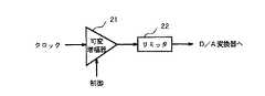
図2には、位相調整手段10の回路構成の一例を示してあり、この位相調整手段10は、可変(利得)増幅器21とリミッタ22とを直列に接続して構成されている。
可変増幅器21は、制御部12から入力される制御信号(例えば制御電圧)に応じて利得(ゲイン)が変化する特性を有しており、クロック源9から入力されるクロック信号を制御部12により制御される利得で増幅し、当該増幅信号をリミッタ22へ出力する。
【0119】
リミッタ22は、例えば(固定的に設定された)所定の閾値以上のレベルを有する信号が入力される場合に当該信号のレベルを全て同一のレベル(例えば当該閾値に相当するレベル)として出力する特性を有しており、可変増幅器21から入力される増幅信号のレベルを当該特性により制限し、当該制限した増幅信号をD/A変換器7(位相調整手段11に関してはD/A変換器8)へ出力する。
【0120】
図3を参照して、上記図2に示した回路の動作例を示す。なお、同図(a)〜同図(d)中のグラフでは、横軸は時刻を示しており、縦軸は信号の電圧レベルを示している。
具体的に、同図(a)には、クロック源9から出力されるクロック信号の波形の一例を示してある。
また、同図(b)には、可変増幅器21により増幅されたクロック信号の波形の一例を示してある。
【0121】
また、同図(c)には、増幅されたクロック信号がリミッタ22により処理された後の信号の波形の一例を実線で示してあり、また、説明の便宜上から、当該増幅されたクロック信号の波形の一例を点線で示してあるとともに、リミッタ22に設定された閾値の一例を示してある。同図(d)に示されるように、リミッタ22の閾値以上のレベルとなる入力信号は全て所定のレベル(オン状態)にクリップされるため、リミッタ22からは矩形波の信号が出力される。
【0122】
また、同図(d)には、同図(c)に示した場合と比べて可変増幅器21の利得が低く制御された場合に関して、増幅されたクロック信号がリミッタ22により処理された後の信号の波形の一例を実線で示してあり、また、説明の便宜上から、当該増幅されたクロック信号の波形の一例を点線で示してあるとともに、リミッタ22に設定された閾値(同図(c)の場合と同じ値)の一例を示してある。
【0123】
同図(d)に示されるように、可変増幅器21の利得が比較的低い場合には、リミッタ22に入力される正弦波のレベルが相対的に或る程度大きくなったところでそのレベルがクリップされる。このように、可変増幅器21の利得を変化させると、リミッタ22から出力される信号がオン状態となる時間の幅が当該利得に応じて変化する。
【0124】
例えば、同図(c)及び同図(d)中に破線で示したように、可変増幅器21の利得が異なる2つの場合に関してリミッタ22により増幅信号のレベルがクリップされる時間を比較すると、リミッタ22から出力される信号の位相が当該利得に応じてずれることになる。
【0125】
本例では、制御部12により可変増幅器21の利得(つまり、増幅後のクロック信号の電圧レベル)を制御して、位相が変移させられたクロック信号(タイミング信号)を生成して当該信号をD/A変換器7の入力クロックとして用いることにより、当該D/A変換器7の動作タイミングを(微)調整することが可能である。つまり、D/A変換器7は例えば入力されるクロック信号の立ち上がり(或いは、立ち下がり)のタイミングで動作することから、当該D/A変換器7から(アナログ)制御信号が出力されるタイミングを微妙(微小)に変移させて調整することが可能となる。
【0126】
以上のように、上記図2に示したような位相調整手段10、11の構成では、制御部12から可変増幅器21の利得を制御することにより、種々な位相を有するクロック信号(タイミング信号)を生成することができ、これにより、遅延時間を微妙(微小)に調整することができる。
【0127】
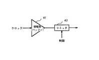
また、図4には、位相調整手段10の回路構成の他の一例を示してあり、この位相調整手段10は、増幅器31と比較器(コンパレータ)32とを直列に接続して構成されている。
増幅器31は、例えば出力信号の(電圧)レベルが一定となる(例えば増幅のゲインが一定である)特性を有しており、クロック源9から入力されるクロック信号を増幅し、当該増幅信号を比較器32へ出力する。
【0128】
なお、上記のような特性を有する増幅器31は一般にバッファと呼ばれており、このような増幅器31は、例えば位相調整手段10がクロック源9から物理的に近い位置に配置されるという条件や、位相調整手段10への入力信号(本例では、クロック源9からのクロック信号)に減衰が生じないという条件等が満たされる場合には、回路構成中から省略することが可能である。
【0129】
比較器32は、増幅器31から出力される増幅信号を入力するとともに、制御部12から出力される制御信号を入力し、これら2つの信号のレベルの大小を比較して、当該比較結果を“1”値(例えば、Highレベル)と“0”値(例えば、Lowレベル)とから成る信号としてD/A変換器7へ出力する。
【0130】
具体的には、本例では、制御部12から比較器32に入力される制御信号の(電圧)レベルは当該比較器32における閾値として用いられており、当該比較器32では、増幅器31から入力される信号の(電圧)レベルが当該閾値以上である場合にオン信号(本例では、“1”値の信号)を出力する一方、当該レベルが当該閾値未満である場合にオフ信号(本例では、“0”値の信号)を出力する。
【0131】
また、図5には、位相調整手段10の回路構成の他の一例を示してあり、この位相調整手段10は、増幅器41とリミッタ42とを直列に接続して構成されている。
増幅器41は、例えば出力信号の(電圧)レベルが一定となる(例えば増幅のゲインが一定である)特性を有しており、クロック源9から入力されるクロック信号を増幅し、当該増幅信号をリミッタ42へ出力する。
なお、上記図4に示した回路構成に関して述べたのと同様に、このような増幅器41は、所定の条件が満たされる場合には、回路構成中から省略することが可能である。
【0132】
リミッタ42は、制御部12から入力される制御信号に応じて閾値が変化する特性を有するとともに、当該閾値以上のレベルを有する信号が入力される場合に当該信号のレベルを全て同一のレベル(例えば当該閾値に相当するレベル)として出力する特性を有しており、増幅器41から入力される増幅信号のレベルを当該特性により制限し、当該制限した増幅信号をD/A変換器7へ出力する。
【0133】
具体的には、本例では、制御部12からの制御(電圧)によりリミッタ42の閾値が変化させられ、当該リミッタ42では、増幅器41から入力される信号の(電圧)レベルが当該閾値以上である場合に、当該レベルを制限して所定の(電圧)レベルのオン信号(本例では、“1”値の信号)を出力する。
【0134】
図6を参照して、上記図4や上記図5に示した回路の動作例を示す。ここで、上記図4に示した回路の動作と上記図5に示した回路の動作とは同様な特徴を有するため、ここでは、これら2つの回路の動作例をまとめて説明する。なお、同図(a)〜同図(g)中では、横方向は時刻を示しており、縦方向は信号の電圧レベルを示している。また、同図(f)及び同図(g)については後述する。
【0135】
具体的に、同図(a)には、クロック源9から出力されて増幅器(増幅器31や増幅器41)に入力されるクロック信号の波形の一例を示してある。
また、同図(b)や同図(d)には、増幅器(増幅器31や増幅器41)により増幅された(例えば固定的に設定された多少のゲインが与えられた)クロック信号の波形の一例を示してある。
【0136】
また、同図(c)や同図(e)には、(比較器32やリミッタ42の)閾値を(同図(c)と同図(d)とで)変化させた場合に、位相調整手段10(比較器32やリミッタ42)からD/A変換器7へ出力される信号の波形の一例を実線で示してあり、また、説明の便宜上から、増幅器(増幅器31や増幅器41)により増幅されたクロック信号の波形の一例を点線で示してあるとともに、(比較器31やリミッタ41に)設定された閾値の一例を点線で示してある。
【0137】
同図(c)や同図(e)に示されるように、上記図4や上記図5に示したような位相調整手段10、11の構成では、制御部12から比較器32の閾値やリミッタ42の閾値を制御することにより、種々な位相を有するクロック信号(タイミング信号)を生成することができ、これにより、遅延時間を微妙(微小)に調整することができる。つまり、この例では、増幅器(増幅器31や増幅器41)での利得を変化させるのではなく、後段の比較器32へのリファレンス電圧の値(閾値)や、後段のリミッタ42の閾値を変化させることにより、クロック信号の位相を変化させることができる。
【0138】
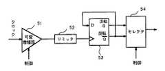
また、図7には、位相調整手段10の回路構成の他の一例を示してあり、この位相調整手段10は、可変(利得)増幅器51とリミッタ52とフリップフロップ(D−FF)53とセレクタ54とを直列に接続して構成されている。
【0139】
このような回路構成では、フリップフロップ53によりクロック信号(タイミング信号)のデューティを制御することなどが実現される。つまり、上述のように、D/A変換器7、8は、入力されるクロック信号(タイミング信号)の立ち上がりや立ち下がりで動作するが、現実のD/A変換器においては、例えば入力クロックのHighレベル領域やLowレベル領域に対して最低必要時間(デューティ)が規定されているものがある。この場合、例えば上記図2や上記図4や上記図6に示したような回路構成では、デューティが変動してしまうことから位相調整手段10により変移可能な位相が制限されてしまうことが生じ得る。そこで、本構成では、上述のようにフリップフロップ53によりデューティを整形する。
【0140】
可変増幅器51の機能や動作は例えば上記図2に示した可変増幅器21の機能や動作と同様であり、可変増幅器51は、クロック源9から入力されるクロック信号を制御部12により制御される利得で増幅し、当該増幅信号をリミッタ52へ出力する。
【0141】
リミッタ52の機能や動作は例えば上記図2に示したリミッタ22の機能や動作と同様であり、リミッタ52は、可変増幅器51から入力される増幅信号のレベルを所定の閾値をもって制限し、当該制限した増幅信号をフリップフロップ53へ出力する。
【0142】
フリップフロップ53は、2つの入力端と2つの出力端を有しており、リミッタ52から出力される信号を一方の入力端から入力するとともに、一方の出力端(反転信号の出力端)から出力される反転信号を他方の入力端から入力し、当該一方の出力端から当該他方の入力端及びセレクタ54へ当該反転信号を出力するとともに、他方の出力端からセレクタ54へ正転信号を出力する。
【0143】
ここで、上記した正転信号は、例えばリミッタ52からフリップフロップ53に入力される信号のデューティが当該フリップフロップ53により変化させられた信号であり、また、上記した反転信号は、更に当該信号のオンオフが反転させられた信号である。
また、フリップフロップ53は、一般にデューティを50%にするために利用されており、本例のような構成では、後述する図8を用いて示すように、クロック信号(タイミング信号)のデューティを50%にすることができる。
【0144】
セレクタ54は、2つの入力端と1つの出力端を有しているとともに、制御部12からの制御信号に応じていずれか一方の入力端から入力される信号(のみ)を選択的に出力端から出力するように出力信号を切り替える機能を有している。そして、セレクタ54は、フリップフロップ53の前記一方の出力端から出力される反転信号を一方の入力端から入力するとともに、当該フリップフロップ53の前記他方の出力端から出力される正転信号を他方の入力端から入力し、制御部12からの制御に従って、当該反転信号或いは当該正転信号のいずれか一方をD/A変換器7へ出力する。
【0145】
図8を参照して、上記図7に示した回路の動作例を示す。なお、同図(a)〜同図(g)中では、横方向は時刻を示しており、縦方向は信号の電圧レベルを示している。
具体的に、同図(a)には、クロック源9から出力されて可変増幅器51に入力されるクロック信号の波形の一例を示してある。
また、同図(b)や同図(d)には、(同図(b)と同図(d)とで)異なる利得を用いて可変増幅器51により増幅されたクロック信号の波形の一例を示してある。
【0146】
また、同図(c)や同図(e)には、それぞれ同図(b)や同図(d)と対応して、増幅されたクロック信号がリミッタ52により処理された後の信号の波形の一例を実線で示してあり、また、説明の便宜上から、当該増幅されたクロック信号の波形の一例を点線で示してあるとともに、リミッタ52に設定された閾値の一例を点線で示してある。
【0147】
同図(c)や同図(e)に示されるように、可変増幅器51の利得を変化させると、生成されるクロック信号(タイミング信号)の位相が変化すると同時に、当該クロック信号のデューティが変化してしまう。
【0148】
そこで、本例では、フリップフロップ53により、クロック信号(タイミング信号)のデューティを50%にする。
具体的に、同図(f)には、リミッタ52から出力される信号の波形の一例を示してあり、この段階では、当該信号のデューティは可変増幅器51から出力される信号の(電圧)レベルに依存して種々な値となる。
【0149】
同図(g)には、フリップフロップ53から例えば正転信号として出力される信号の波形の一例を実線で示してあるとともに、説明の便宜上から、当該フリップフロップ53の前記一方の入力端に入力される信号の波形の一例(同図(f)に示したもの)を点線で示してある。同図(g)に示されるように、フリップフロップ53から信号が出力される段階では、当該信号のデューティは50%となっている。つまり、フリップフロップ53では、例えばリミッタ52から入力される信号の各立ち上がりの時点でオンオフを繰り返す信号を出力し、このような信号のデューティは50%となる。
【0150】
また、本例では、位相調整手段10、11から出力されるクロック信号(タイミング信号)の立ち上がり時間(或いは、立ち下がり時間)を変移させることで当該信号の位相を変移させているが、上記したフリップフロップ53までの回路構成では、位相を180°以上変移させることは難しい。
【0151】
そこで、本例では、セレクタ54により、クロック信号(タイミング信号)の位相を例えば360°の範囲で制御することを可能とする。
つまり、本例では、一般にフリップフロップ53からは互いに立ち上がり時間と立ち下がり時間とが反転した正転信号及び反転信号が出力されることを利用しており、具体的には、制御部12によりセレクタ54を制御して当該正転信号と当該反転信号とのいずれか一方を当該セレクタ54から出力することにより、広い範囲での位相調整を実現することができる。
【0152】
なお、上記図7に示したような回路構成では、上記図8(g)に示されるように各位相調整手段10、11から出力されるクロック信号(タイミング信号)の周期が当該各位相調整手段10、11に入力される(クロック源9からの)クロック信号の周期の2倍となるため、例えばD/A変換器7、8の入力クロックに必要とされる所要レートの2倍の速度(つまり、半分の周期)を有するクロック信号を出力するクロック源9が用いられる。具体例として、D/A変換器7、8によるD/A変換のレートが80MHzであれば、160MHzのクロック信号を出力するクロック源9が用いられる。
【0153】
また、上記図7では、上記図2に示したのと同様な回路構成にフリップフロップ53やセレクタ54を追加した構成を示したが、これと同様に、例えば上記図4に示した比較器32の後段や上記図5に示したリミッタ42の後段にフリップフロップを備えてクロック信号(タイミング信号)のデューティを調整することも可能であり、また、更に、例えばフリップフロップの後段にセレクタを備えて当該クロック信号に関して調整可能な位相範囲を拡大することも可能である。
【0154】
なお、上記図6(f)には、例えば上記図8(f)に示したのと同様に、比較器32やリミッタ42から出力される信号の波形の一例を示してあり、また、上記図6(g)には、例えば上記図8(g)に示したのと同様に、当該信号のデューティがフリップフロップにより50%に変換された信号の波形の一例を実線で示してあるとともに、当該変換前の信号の波形の一例(図6(f)に示したもの)を点線で示してある。
【0155】
次に、図9を参照して、各位相調整手段10、11を制御部12により制御して(相対)遅延時間を調整する仕方の一例として、摂動法を示す。
すなわち、本例のプリディストーションによる歪補償は、(増幅器4の)被増幅信号の包絡線に合わせて行われる。このように、測定された包絡線に合わせた歪補償を被増幅信号に対して行う場合には、歪補償の制御系(制御部12やD/A変換器7、8側の系)と被増幅信号が流れる主信号系(可変減衰器2や可変移相器3側の系)との間の(相対的な)遅延時間を調整することが必要である。
【0156】
仮に、上記した遅延時間の調整が不完全であれば、その影響により、最終段に備えられた増幅器4から出力される信号中に歪成分が残存することになる。そして、このような歪成分の有無などは例えばスペクトルアナライザ等を用いて容易に判断することが可能であり、本例の制御部12では、歪抽出手段6を用いて当該歪成分の量をモニタすることにより、遅延時間の存在に起因した歪残存量を検出している。
【0157】
以下で、上記のような遅延時間を調整する仕方の一例として、摂動法による調整例を示す。
具体的には、摂動法では、次の(1)〜(4)の処理を繰り返して行うことにより、遅延時間を調整する。
【0158】
(1)現時点での遅延時間T(後述する(4)の処理の後には、T=T’)における上記した歪成分の量をP0として保存する。
(2)遅延時間を(+τ)だけ調整し(つまり、遅延時間を更に遅らせて(T+τ)とし)、その時の歪成分の量をP+として保存する。
(3)上記(2)の処理と共に、遅延時間を(−τ)だけ調整し(つまり、遅延時間を進ませて(T−τ)とし)、その時の歪成分の量をP−として保存する。
(4)上記した歪量P+と上記した歪量P−との大小を比較して、これらの中で小さい方の歪量(P+、或いは、P−)に対応した遅延時間を新たな遅延時間T’(T’=T+τ、或いは、T’=T−τ)として保存する。
【0159】
上記した(1)〜(4)の処理を繰り返して行うと、更新される遅延時間Tが最適な状態に近づいていき、上記した歪量P0と上記した歪量P+、P−との差が小さくなっていく。
また、例えば上記した歪量P0と上記した歪量P+、P−との差が小さくなる度に、上記(2)の処理や上記(3)の処理で用いられる調整時間を(±τ)から(±τ/2)等へと変更して当該調整時間を半減していくようにすると、遅延時間の調整をアダプティブに行うことが可能となって好ましい。
【0160】
ここで、上記図9には、摂動法により遅延時間を調整するイメージの一例を示してあり、同図中の横軸は(相対)遅延時間を示しており、上方向の縦軸は歪成分の量を示しており、下方向の縦軸は経過時間を示している。また、同図には、残存する遅延時間に起因して生じる歪成分(歪抽出手段6により抽出される歪成分)の量を示す曲線Pを示してあり、当該歪成分量が最小となる位置で遅延時間がゼロとなる。
【0161】
具体例として、摂動法では、まず、現時点での遅延時間Tの位置を開始点として設定する(同図中の▲1▼)。
次いで、次の経過時間において、遅延時間(T+τ)の位置の歪量と遅延時間(T−τ)の位置の歪量との大小を比較し、これらの中で小さい方の歪量に対応した例えば遅延時間(T+τ)を更新後の遅延時間T’として選択する(同図中の▲2▼)。
【0162】
次いで、次の経過時間において、遅延時間(T+τ+τ)の位置の歪量と遅延時間(T+τ−τ)の位置の歪量との大小を比較し、これらの中で小さい方の歪量に対応した例えば遅延時間(T+τ+τ)を更新後の遅延時間T’として選択する(同図中の▲3▼)。
【0163】
そして、更新される遅延時間が最適な遅延時間(ゼロ)に近づいてきて歪成分量が収束してきたことを判定したことに応じて、次の経過時間では、遅延時間(T+τ+τ+τ/2)の位置の歪量と遅延時間(T+τ+τ−τ/2)の位置の歪量との大小を比較し、これらの中で小さい方の歪量に対応した例えば遅延時間(T+τ+τ−τ/2)を更新後の遅延時間T’として選択する(同図中の▲4▼)。
以上のような処理を繰り返して行うことにより、更新される遅延時間を次第に最適な遅延時間(ゼロ)に近づけることができる。
【0164】
なお、上記手段で述べたように、遅延時間は、例えば[1/{キャリア周波数間隔×キャリア数×n}]秒以内の時間誤差(つまり、本例では、最適な遅延時間であるゼロからの差)で調整されるのが好ましい。ここで、キャリア周波数間隔やキャリア数は本例の増幅装置により処理される送信信号に関する値が用いられ、また、nとしては8以上の正の数が設定される。また、(キャリア周波数間隔×キャリア数)は送信信号の帯域に相当する。
【0165】
以上のように、本例の増幅装置に備えられたプリディストータでは、増幅器4により増幅する送信信号に対して可変減衰器2や可変移相器3により発生させる歪(振幅歪や位相歪)の量を制御するタイミングを位相調整手段10、11により調整することにより、当該タイミングを微妙(微小)に調整することが可能となり、これにより、高精度な歪補償を実現することができる。
【0166】
具体的には、例えば微小な遅延時間の存在に起因してプリディストーションが正常に行われないようなことを回避することができ、また、例えば従来において長時間を要していた微小遅延時間の調整処理を短時間で行うことが可能となり、また、これらの結果として、例えば装置のコストを低減させることも可能である。
【0167】
ここで、本例では、増幅器4が本発明に言う(歪補償対象となる)増幅器に相当する。
また、本例では、可変減衰器2や可変移相器3の機能により、本発明に言う歪発生手段が構成されている。なお、本例では、可変減衰器2や可変移相器3により、外部から入力されるアナログ制御信号に応じて発生させる歪の量が変化する回路が構成されている。
【0168】
また、本例では、レベル検出部5の機能により、本発明に言う信号レベル検出手段が構成されている。
また、本例では、制御部12や2つのD/A変換器7、8の機能により、本発明に言う歪量制御手段が構成されている。
また、本例では、クロック源9や2つの位相調整手段10、11の機能により、本発明に言う制御タイミング調整手段が構成されている。
【0169】
また、本例では、2つのD/A変換器7、8の機能により、本発明に言うD/A変換手段が構成されている。
また、本例では、クロック源9の機能により、本発明に言うクロック信号発生手段が構成されている。
また、本例では、2つの位相調整手段10、11がタイミングを調整したクロック信号(タイミング信号)を生成する機能により、本発明に言うタイミング信号生成手段が構成されている。
【0170】
次に、本発明の第2実施例に係る(歪補償)増幅装置を図10を参照して説明する。
なお、本例の増幅装置は、本発明に係る歪補償装置の一実施例であるプリディストータを備えており、このプリディストータによりプリディストータ型歪補償方式を用いて増幅器で発生する歪を補償する。
【0171】
上記図10には、本例のプリディストータを備えた増幅装置(プリディストーション機能付き増幅器)の回路構成例を示してある。なお、この増幅装置は、例えば移動無線通信システムの基地局装置や中継局装置の送信部に設けられており、送信対象となる信号(送信信号)を送信機から入力し、当該信号を増幅器により増幅してアンテナへ出力する。
【0172】
同図に示されるように、本例の増幅装置には、遅延手段61と、可変減衰器62と、可変移相器63と、増幅器64と、レベル検出部65と、歪抽出手段66と、2つのメモリ67、68と、2つのD/A変換器69、70と、クロック源71と、2つの位相調整手段72、73と、制御部74とが備えられている。
【0173】
ここで、本例の増幅装置の構成は、可変減衰器62や可変移相器63を制御するためのメモリ67、68が制御部74の外部に設けられているといった点を除いては、例えば上記第1実施例の図1に示した増幅装置の構成と同様である。このため、以下では、上記第1実施例の図1に示した増幅装置と同様な構成部分については詳しい説明を省略し、当該増幅装置とは異なる構成部分について詳しく説明する。
【0174】
すなわち、本例の増幅装置では、可変減衰器62を制御するための構成として、メモリ67が制御部74とD/A変換器69との間に設けられているとともに、可変移相器63を制御するための構成として、メモリ68が制御部74とD/A変換器70との間に設けられている。また、本例の増幅装置では、レベル検出部65により信号のレベルを検出した結果がデジタル値として2つのメモリ67、68へ出力される。
【0175】
一方のメモリ67は、可変減衰器62を制御するためのルックアップテーブル(LUT:Look Up Table)を有しており、このルックアップテーブルには、レベル検出部65から出力される(検出結果の)デジタル値と、可変減衰器62で発生させる振幅歪を制御するための(デジタル)制御値とが対応付けられて格納されている。ここで、制御値としては、当該制御値と対応付けられるデジタル値(検出結果)が得られた場合に増幅器64で発生する振幅歪をプリディストーションにより補償することができる振幅歪(前記振幅歪とは逆特性の振幅歪)を実現する値が、例えば予め計算(或いは測定等)されて格納されている。
【0176】
同様に、他方のメモリ68は、可変移相器63を制御するためのルックアップテーブル(LUT)を有しており、このルックアップテーブルには、レベル検出部65から出力される(検出結果の)デジタル値と、可変移相器63で発生させる位相歪を制御するための(デジタル)制御値とが対応付けられて格納されている。ここで、制御値としては、当該制御値と対応付けられるデジタル値(検出結果)が得られた場合に増幅器64で発生する位相歪をプリディストーションにより補償することができる位相歪(前記位相歪とは逆特性の位相歪)を実現する値が、例えば予め計算(或いは測定等)されて格納されている。
【0177】
このように、上記した一方のメモリ67は補正AM−AM特性を記憶するルックアップテーブルを有しているとともに、上記した他方のメモリ68は補正AM−PM特性を記憶するルックアップテーブルを有している。そして、これらのルックアップテーブルは、レベル検出部65から入力されるデジタル値(検出結果)をアドレスとして、当該入力アドレスと対応した記憶値(制御値)をそれぞれのD/A変換器69、70へ出力する処理を実行し、本例では、このような処理により、可変減衰器62や可変移相器63による歪発生量が制御される。
【0178】
なお、本例のD/A変換器69、70は、それぞれのメモリ67、68から入力されるデジタル制御信号をアナログ制御信号へ変換して、当該アナログ制御信号を可変減衰器62や可変移相器63へ出力する。
【0179】
また、本例では、例えば抽出手段66を用いて検出される歪成分のレベルに基づいて、上記した各メモリ67、68の記憶内容が制御部74により適応的に書き換えられる構成としており、このような構成により、例えば温度特性の変化や経年変化によって生じる微小な遅延時間の誤差に対処することが可能なプリディストーションを実現することができる。
【0180】
以上のように、本例の増幅装置では、可変減衰器62や可変移相器63を制御するためのメモリ67、68が制御部74とは別個な構成とされて当該制御部74の外部に配置されているため、当該メモリ67、68への高速なアクセスが可能となって、処理の効率を向上させることができる。
ここで、本例では、2つのメモリ67、68の機能により、本発明に言うメモリ手段が構成されている。
【0181】
一例として、本例の増幅装置では、80MHzで動作するデジタル部を想定しているが、一般に、80MHz(12.5nsec)程度でのD/A変換処理が必要となる場合には、制御部74から直接的にアクセスすることが困難であることが生じ得る。なお、この理由は、制御部74はデジタル信号処理器(DSP)から構成されることが多く、デジタル信号処理器では入出力レート(外部ハードウエアのアクセススピード)として30MHz程度が限界だからである。
【0182】
これに対して、本例の増幅装置では、上述したように、メモリ67、68を制御部74の外部に配置することで高速なアクセスが可能となり、例えば広帯域の送信信号を処理するような場合においても、微妙(微小)な位相調整(D/A変換のタイミング調整)を容易に実現することができる。
【0183】
ここで、本発明に係る歪補償装置の構成としては、必ずしも以上に示したものに限られず、種々な構成が用いられてもよい。
例えば、プリディストーションを行うための可変減衰器と可変移相器との配置の順序は任意である。また、例えば、(歪補償の対象となる)増幅器の出力信号から歪成分の信号(誤差信号)を取得することを実現するための構成や、レベル検出部の構成としては、種々な構成が用いられてもよい。
【0184】
また、例えば、以上の実施例では示さなかったが、D/A変換器と可変減衰器との間やD/A変換器と可変移相器との間に低域通過フィルタ(LPF)を備えて、これらのD/A変換器からの出力信号を当該低域通過フィルタにより平滑化する構成が用いられてもよく、このような低域通過フィルタの有無は、例えば装置の使用状況等に応じて任意に設定されてもよい。
【0185】
また、本発明に係る歪補償装置の適用分野としては、必ずしも以上に示した分野に限られず、本発明は種々な分野に適用することが可能なものである。
一例として、本発明に係る歪補償装置は、デジタル処理を用いたプリディストータ型歪補償方式を採用する装置に適用することも可能であり、また、アナログ処理を用いたプリディストータ型歪補償方式を採用する装置に適用することも可能である。
【0186】
また、本発明に係る歪補償装置により行われる各種の処理としては、例えばプロセッサやメモリ等を備えたハードウエア資源においてプロセッサがROMに格納された制御プログラムを実行することにより制御される構成が用いられてもよく、また、例えば当該処理を実行するための各機能手段が独立したハードウエア回路として構成されてもよい。
また、本発明は上記の制御プログラムを格納したフロッピーディスクやCD−ROM等のコンピュータにより読み取り可能な記録媒体として把握することもでき、当該制御プログラムを記録媒体からコンピュータに入力してプロセッサに実行させることにより、本発明に係る処理を遂行させることができる。
【0187】
【発明の効果】
以上説明したように、本発明に係る歪補償装置によると、例えば増幅器により増幅される信号に対して可変減衰器や可変移相器により発生させる振幅歪や位相歪の量を、当該増幅器により増幅される信号のレベルの検出結果に基づいて制御するに際して、当該増幅器で発生する歪が大きく補償されるように当該制御のタイミングを調整するようにしたため、当該タイミングを微妙(微小)に調整することが可能となり、これにより、高精度な歪補償を実現することができる。
【図面の簡単な説明】
【図1】本発明の第1実施例に係るプリディストータを備えた増幅装置の回路構成例を示す図である。
【図2】位相調整手段の回路構成例を示す図である。
【図3】位相調整手段の動作の一例を説明するための図である。
【図4】位相調整手段の回路構成例を示す図である。
【図5】位相調整手段の回路構成例を示す図である。
【図6】位相調整手段の動作の一例を説明するための図である。
【図7】位相調整手段の回路構成例を示す図である。
【図8】位相調整手段の動作の一例を説明するための図である。
【図9】摂動法により遅延時間を調整するイメージの一例を示す図である。
【図10】本発明の第2実施例に係るプリディストータを備えた増幅装置の回路構成例を示す図である。
【図11】従来例に係るプリディストータを備えた増幅装置の回路構成例を示す図である。
【図12】歪が発生していない信号のスペクトラムの一例を示す図である。
【図13】歪が発生した信号のスペクトラムの一例を示す図である。
【図14】歪を補償した信号のスペクトラムの一例を示す図である。
【図15】遅延時間が振幅歪の補正に対して与えてしまう影響に関する計算機シミュレーションの結果の一例を示す図である。
【図16】遅延時間が位相歪の補正に対して与えてしまう影響に関する計算機シミュレーションの結果の一例を示す図である。
【符号の説明】
1、61・・遅延手段、 2、62・・可変減衰器(アッテネータ)、
3、63・・可変移相器、 4、31、41、64・・増幅器、
5、65・・レベル検出部、 6、66・・歪抽出手段、
7、8、69、70・・D/A変換器、 9、71・・クロック源、
10、11、72、73・・位相調整手段、 12、74・・制御部、
21、51・・可変増幅器、 22、42、52・・リミッタ、
32・・コンパレータ、 53・・フリップフロップ、 54・・セレクタ、
67、68・・メモリ、[0001]
TECHNICAL FIELD OF THE INVENTION
The present invention relates to a distortion compensating device that compensates for distortion generated by an amplifier, and in particular, adjusts timing for controlling the amount of distortion generated for a signal amplified by the amplifier, thereby achieving high-precision distortion compensation. The present invention relates to a distortion compensation device to be realized.
[0002]
[Prior art]
For example, in a mobile radio communication system such as a mobile phone system, it is possible to perform radio communication with a mobile station device existing up to an end of an area (cell) controlled by a base station device, and depending on a communication condition. Since the base station device simultaneously transmits a radio signal to a plurality of mobile station devices (a plurality of users), the base station device needs to transmit a signal with high power. Similarly, a relay station device (relay amplifier) that receives and amplifies a signal wirelessly transmitted from the base station device and wirelessly transmits the amplified signal to the mobile station device also transmits a signal with high power. It is necessary.
[0003]
For this reason, in the base station apparatus and the relay station apparatus as described above, a signal to be transmitted (for example, a power amplifier (PA)) capable of covering a physical distance to an end of a cell (for example, a power amplifier). (A modulated wave) is amplified to a desired level. However, such an amplifier exhibits a nonlinear response (AM-AM conversion or AM-PM conversion) characteristic near the limit point (saturation point) of the element, and causes nonlinear distortion. There's a problem.
[0004]
In addition, for example, the Radio Law stipulates that a strict band limitation be imposed on a person who performs various wireless communication services in order to eliminate the influence between different services that perform wireless communication using adjacent bands. .
[0005]
Therefore, as a method of compensating for the nonlinear distortion generated in the amplifier as described above, conventionally, for example, a distortion having a characteristic opposite to that of the nonlinear distortion generated in the amplifier (that is, canceling out the nonlinear distortion) is used in the previous stage. A predistorter type distortion compensation method for compensating the non-linear distortion by generating the distortion is used.
[0006]
As a method of compensating for the nonlinear distortion as described above, there are other distortion compensation methods such as a feedforward distortion compensation method and a negative feedback distortion compensation method. Here, for example, in a feedforward type distortion compensation system, although there is an advantage that operation is stable, a distortion component (generated in a main amplifier) is extracted in a distortion detection loop, and the distortion component is extracted in a distortion compensation loop by a sub-amplifier. It is necessary to perform a process of amplifying the amplified signal and subtracting the amplified signal from the output signal of the main amplifier, so that the circuit becomes complicated, and the power efficiency is reduced by the sub-amplifier. On the other hand, the predistorter type distortion compensation system is particularly advantageous in terms of circuit scale and power supply efficiency because the configuration is relatively simple and no auxiliary amplifier is required.
[0007]
Next, an example of a (distortion compensation) amplification apparatus including a predistorter for performing distortion compensation by the above-described predistorter type distortion compensation method will be described.
FIG. 11 shows an example of a circuit configuration of an amplifying device (amplifier with a pre-distortion function) including a predistorter, and an operation example of the amplifying device is shown with reference to FIG. The amplifying device is provided in the transmitting unit of the base station device or the relay station device as described above, receives a signal to be transmitted (transmission signal) from a transmitter, and amplifies the signal by an amplifier. Output to the antenna.
[0008]
First, a signal to be transmitted, which is output from the transmitter, is input (to the amplifying device), the signal is split into two, and one split signal is input to the
[0009]
Here, FIG. 12 shows an example of a spectrum of a signal at a stage where the signal is input from the transmitter to the amplifying device. In FIG. 12, the horizontal axis indicates the frequency [kHz] of the signal, and the vertical axis indicates the frequency. The signal level is indicated by the power ratio [dB]. As shown in the figure, at this stage, since the distortion by the predistorter (the
[0010]
The
The
[0011]
The
In this example, a predistorter (predistorter) is configured by a
[0012]
The
Here, FIG. 13 shows an example of the spectrum of a signal output from the
[0013]
Such a distortion component causes the predistorter (
Here, FIG. 14 shows an example of a spectrum of a signal output from the
[0014]
The
[0015]
The distortion extracting means 86 is composed of, for example, a directional coupler, and extracts distortion (for example, a part of the amplified signal) included in the amplified signal output from the
The clock source 87 generates a clock signal having a predetermined cycle, and outputs the clock signal to each processing unit that performs digital processing, such as a
[0016]
A D / A (Digital / Analog) converter 88 converts a digital control signal input from a
[0017]
The D /
[0018]
The
[0019]
Specifically, in the non-linear characteristic of the
[0020]
As an example, a corrected amplitude distortion characteristic (a characteristic opposite to the amplitude distortion) for compensating for the amplitude distortion generated in the
[0021]
Further, the
[0022]
By the way, the above-mentioned delay means 81 outputs the timing at which the one distributed signal is processed by the
[0023]
That is, when distortion (amplitude distortion or phase distortion) is generated for a certain signal portion of the input signal by the
[0024]
[Problems to be solved by the invention]
However, for example, the
[0025]
Here, the above-mentioned problems will be described in more detail.
That is, the delay means 81 detects the level of the other distribution signal and performs D / A conversion of the digital control signal according to the detection result, as well as the physical wiring path. It is necessary to adjust the delay time caused by this.
[0026]
As an example, according to the result of studying an amplifying device assumed by the present inventors (this is an example, and the present invention is not limited to the example given here), the adjustment of the delay time is 500 psec ( psec: pico second) = 10-12 Adjustments on the order of seconds are required. If this delay time is adjusted by a semi-rigid cable, for example, a cable of about 10 cm is prepared and adjusted. However, considering that the length of the (circuit) substrate of an electronic device is generally about 30 to 40 cm from end to end, the above-mentioned 10 cm corresponds to a delay time that is easily generated by wiring.
[0027]
In addition, the above-described delay time varies depending on, for example, the parasitic capacitance of the substrate and individual differences between devices used. That is, conventionally, it is necessary to adjust the delay time by, for example, adjusting the length of the cable every time a device (for example, the amplifying device shown in FIG. 11 described above) is created. In addition, the delay time depends on, for example, the temperature characteristics of each electronic device, and when the temperature changes, the delay time also (subtly) changes. In addition, the delay time changes (aging) depending on, for example, the use date of each device.
[0028]
As described above, adjusting the delay time as described above is a very important factor in the production of the device, and it is conventionally difficult to perform such delay time adjustment in minute units. As a result, even if difficult adjustments are made over a long period of time, the apparatus becomes expensive.
[0029]
In addition, an example of a result of a computer simulation regarding the influence of the above-described delay time adjustment error on distortion compensation by a predistorter will be described.
Note that this example shows a case in which a single carrier in a 5 MHz band is used, and the condition regarding the waveform of a signal to be transmitted is, for example, as described in the specification of 3GPP (3rd Generation Partnership Project). Are 50 users and the roll-off rate of the filter for band-limiting the signal is 0.22.
[0030]
Further, parameters for examining the level of the distortion component include a third-order intermodulation distortion component (IM3), a fifth-order intermodulation distortion component (IM5), and the like. In order to achieve this, the level of a distortion component is indicated by an adjacent channel leakage power ratio (ACPR: Adjacent Channel Power Ratio) [dBc], which indicates the level of power leaking to a band adjacent to the used band.
[0031]
Specifically, FIG. 15 shows that the delay time (the relative delay time between the system processing the one distributed signal and the system processing the other distributed signal) is different from the correction (compensation) of the amplitude distortion. An example of the result of a computer simulation regarding the effect to be exerted is shown, and the horizontal axis in the figure indicates a (relative) delay time [× 2 nsec (nsec: nano second = 10).-9 Second)] (for example, the scale of “2” indicates 4 nsec), and the vertical axis indicates the level of the distortion component by the adjacent band leakage power ratio (ACPR) [dBc]. In this simulation, it is assumed that the delay time related to the correction of the phase distortion (for example, by the variable phase shifter 83) is zero.
[0032]
Further, specifically, FIG. 16 shows an example of the result of a computer simulation regarding the effect that the (relative) delay time has on the correction (compensation) of the phase distortion, and the horizontal axis in FIG. The (relative) delay time [× 2 nsec] is shown, and the vertical axis shows the level of the distortion component by the adjacent band leakage power ratio (ACPR) [dBc]. In this simulation, it is assumed that the delay time related to the correction of the amplitude distortion (for example, by the variable phase shifter 83) is zero.
[0033]
As shown in FIG. 15, the influence of the delay time on the compensation for the amplitude distortion is relatively small, while the delay time on the compensation of the phase distortion as shown in FIG. The effect is relatively large, and in any case, as the delay time (adjustment error) increases, the ACPR deteriorates.
[0034]
Here, the reason why the delay time has a greater effect on the compensation for the phase distortion than for the compensation for the amplitude distortion is that, generally, the amplitude variation (AM-AM variation) in the amplifier has a small gain variation amount, while the phase variation in the amplifier is small. This is because the phase variation is large in the distortion (AM-PM variation). That is, with respect to the phase distortion in the amplifier, the fluctuation width is large, so that even if the delay time is slightly shifted, the accuracy of compensation (ACPR in this example) greatly changes.
[0035]
The numerical values presented as the results of the computer simulations shown in FIG. 15 and FIG. 16 are considered to change depending on, for example, the amplification device used in the simulations. It is considered that the tendency to be greatly affected by the delay time as compared with the compensation of the above is the same as the result of this simulation.
[0036]
The present invention has been made to solve the above-described conventional problems. When compensating for distortion generated in an amplifier, for example, the above-described delay time is finely (finely) adjusted by the amplifier. It is an object of the present invention to provide a distortion compensator capable of realizing high-precision distortion compensation by finely adjusting the timing of controlling the amount of distortion generated for a signal to be amplified.
[0037]
[Means for Solving the Problems]
In order to achieve the above object, the distortion compensating device according to the present invention compensates for distortion generated in an amplifier as follows.
That is, for a distortion generating unit that generates at least one of an amplitude and a phase with respect to the signal amplified by the amplifier, the signal level detection unit detects the level of the signal amplified by the amplifier, When the distortion amount control means controls the amount of distortion generated by the distortion generation means based on the level detected by the signal level detection means, the control timing adjustment means controls the distortion so that the distortion generated in the amplifier is largely compensated. The timing for controlling the amount of distortion by the amount control means is adjusted.
[0038]
Therefore, the timing can be finely adjusted, for example, by a novel adjustment method of adjusting the timing of controlling the amount of distortion generated for the signal amplified by the amplifier. Highly accurate distortion compensation can be realized.
[0039]
Here, the amplifier to be subjected to distortion compensation may be of various types, for example, an amplifier composed of a plurality of amplifiers. In the present invention, the amplitude distortion and the phase distortion generated in such an amplifier are to be compensated.
Further, as a degree of compensating the distortion generated in the amplifier, for example, it is preferable to reduce the distortion to zero. However, in the present invention, even if such an aspect (that is, an aspect to reduce to zero) is not necessarily used, What is essential is that the distortion can be reduced.
[0040]
Further, as a mode in which a signal generated by the amplifier causes distortion by the distortion generating means, for example, a mode in which distortion is generated in a signal before being amplified by the amplifier may be used. A mode in which distortion is generated for the signal amplified by the amplifier may be used.
[0041]
Further, the distortion generating means preferably has both a function of generating amplitude distortion and a function of generating phase distortion, for example, a configuration having only a function of generating amplitude distortion, or Alternatively, a configuration having only a function of generating phase distortion may be used.
[0042]
As a mode for detecting the level of the signal amplified by the amplifier by the signal level detection means, for example, a mode for detecting the level of the signal before being amplified by the amplifier may be used. A mode in which the level of the signal after being amplified by is detected may be used.
Further, the level to be detected may be various levels. For example, the level of the signal amplitude and the level of the signal power (normally proportional to the square of the amplitude) can be detected.
[0043]
Further, the distortion amount control means may be configured such that the distortion generation means generates, for example, an amount of distortion (a distortion having a characteristic opposite to that generated by the amplifier) that cancels out the amount of distortion (amplitude distortion or phase distortion) generated in the amplifier. Then, the amount of distortion generated by the distortion generating means is controlled. The amount of distortion (amplitude distortion or phase distortion) generated in the amplifier can be estimated based on, for example, a level detected by a signal level detecting unit.
[0044]
Further, the degree by which the distortion generated in the amplifier is largely compensated by the adjustment by the control timing adjusting means may be various degrees as described above, and specifically, the distortion is not necessarily zero. It is not necessary to compensate, for example, it is only necessary to realize distortion compensation with practically effective accuracy.
Further, adjusting the timing of controlling the amount of distortion by the distortion control unit by the control timing adjustment unit corresponds to, for example, adjusting the delay time as described in the above-described conventional example.
[0045]
Further, the control timing adjusting means always (or, for example, periodically) detects the compensation amount of the distortion generated in the amplifier, and adjusts the distortion amount by the distortion amount controlling means so as to increase the compensation amount. It is preferable to use a configuration in which the control timing is adjusted (always or periodically). For example, a configuration in which the adjustment time is set (fixed) so that distortion generated in the amplifier is largely compensated in advance May be used.
[0046]
In a preferred embodiment of the distortion compensating device according to the present invention, the distortion generating means includes a distortion (amplitude distortion or amplitude distortion) generated in response to an analog control signal input from outside (here, a D / A conversion means described later). It is composed of a circuit that changes the amount of phase distortion (a circuit that changes the amplitude and a circuit that changes the phase).
Further, the distortion amount control unit uses a D / A conversion unit that converts a digital control signal into an analog control signal and outputs the digital control signal at a timing corresponding to a timing signal input from the outside (here, a control timing adjustment unit). It is configured to output a digital control signal to the distortion generator via the D / A converter, thereby controlling the amount of distortion (amplitude distortion or phase distortion) generated by the distortion generator.
[0047]
The control timing adjusting means includes a clock signal generating means for generating a clock signal of a predetermined cycle, and a timing signal generating means for generating a timing signal adjusted in timing from the clock signal generated by the clock signal generating means. A timing signal generated by the timing signal generator is output to the D / A converter to adjust the timing for controlling the amount of distortion (amplitude distortion or phase distortion) by the distortion amount controller. I do.
[0048]
In a preferred embodiment of the distortion compensating apparatus according to the present invention, the distortion amount control means further controls the signal level and the control value (the amount of distortion (amplitude distortion or phase distortion) generated by the distortion generating means). And a control value corresponding to the level detected by the signal level detection means as a digital control signal from the memory means to the D / A conversion means. The amount of distortion (amplitude distortion or phase distortion) generated by the distortion generating unit is controlled by outputting the signal to the distortion generating unit via the control unit.
[0049]
In one aspect of the distortion compensating apparatus according to the present invention, the timing signal generating unit includes a variable amplifier that amplifies a clock signal generated by the clock signal generating unit with a variable gain, and a signal amplified by the variable amplifier. And a limiter that limits the level to a predetermined level when the level is equal to or higher than a predetermined threshold, and outputs the limited level. Is a timing signal.
[0050]
Here, various values may be used as the predetermined threshold value according to, for example, the usage status of the device.
Also, the predetermined level may be various levels, and for example, the predetermined threshold (the same level as the above) can be used.
[0051]
In another aspect of the distortion compensating apparatus according to the present invention, the timing signal generating unit includes an on signal when the level of the clock signal generated by the clock signal generating unit using the variable threshold is equal to or higher than the threshold. While using a comparator that outputs an off signal when the level of the clock signal is less than the threshold, and that the on / off timing is adjusted by adjusting the threshold of the comparator. Is the timing signal.
[0052]
Here, various values may be used as the threshold value according to, for example, the usage status of the device.
For example, when a digital signal composed of a “1” value and a “0” value is taken as an example, the above-mentioned ON signal corresponds to, for example, a signal of a “1” value (or a signal of a “0” value). The above-mentioned off signal corresponds to, for example, a signal of “0” value (or a signal of “1” value).
[0053]
In another aspect of the distortion compensation apparatus according to the present invention, when the level of the clock signal generated by the clock signal generation unit using the variable threshold is equal to or higher than the threshold, Is limited to a predetermined level and is output using a limiter. The output signal from the limiter whose level limit timing is adjusted by adjusting the threshold value of the limiter is used as a timing signal.
[0054]
Here, various values may be used as the threshold value according to, for example, the usage status of the device.
Also, the predetermined level may be various levels, and for example, the predetermined threshold (the same level as the above) can be used.
[0055]
In one aspect of the distortion compensation device according to the present invention, the duty of the timing signal (the ratio of the on-state to the off-state of the signal) can be changed using a flip-flop.
That is, the timing signal generating means further uses a flip-flop which receives the output signal (the output signal from the above-mentioned limiter or the above-mentioned comparator) whose timing has been adjusted and outputs a signal whose duty has been changed. And an output signal from the flip-flop is used as a timing signal.
[0056]
In another aspect of the distortion compensation apparatus according to the present invention, the duty of the timing signal can be changed using a flip-flop, and the timing of the timing signal can be adjusted (with a larger range) using a selector. .
That is, the timing signal generating means further inputs the output signal (the output signal from the above-described limiter or the above-mentioned comparator) whose timing has been adjusted, and inverts the signal whose duty has been changed and the on / off state of the signal. A flip-flop that outputs a signal that has been changed (that is, a signal whose on-off is inverted while changing the duty of the output signal) and a selector that selects and outputs one of two signals output from the flip-flop And the output signal from the selector is used as a timing signal.
[0057]
In a preferred embodiment of the distortion compensating apparatus according to the present invention, the distortion generating means includes: a variable attenuator that changes the amplitude of a signal amplified by the amplifier to generate amplitude distortion on the signal; And a variable phase shifter that changes the phase of the signal to be generated and generates phase distortion for the signal.
In addition, the distortion amount control means controls the amount of amplitude distortion generated by the variable attenuator by controlling the amount of amplitude change by the variable attenuator, and controls the amount of phase change by the variable phase shifter. The amount of phase distortion generated by the variable phase shifter is controlled.
[0058]
Further, the control timing adjusting means is responsive to a difference between the timing at which the signal (the signal amplified by the amplifier) is processed by the variable attenuator and the timing at which the signal is processed by the variable phase shifter. The timing for controlling the amount of amplitude distortion and the timing for controlling the amount of phase distortion by the distortion amount control means are shifted from each other (for example, a time corresponding to the deviation).
[0059]
Here, the connection between the means for generating amplitude distortion (here, a variable attenuator) for the signal amplified by the amplifier and the means for generating phase distortion for this signal (here, a variable phase shifter). The order may be arbitrary, that is, the phase distortion may be generated after generating the amplitude distortion for the signal, or the amplitude distortion may be generated after generating the phase distortion for the signal. May be generated.
[0060]
In a preferred embodiment, the distortion compensating apparatus according to the present invention is provided in a wireless transmitting apparatus that wirelessly transmits a signal and compensates for distortion generated by an amplifier that amplifies a signal to be transmitted by the wireless transmitting apparatus. Then, the control timing adjustment means uses the distortion amount control means with an error of seconds equal to or less than the reciprocal value of a value obtained by multiplying the band of the signal to be transmitted (eg, a value obtained by multiplying the carrier frequency interval by the number of carriers) by eight. Adjust the timing to control the amount of distortion.
[0061]
Here, various devices may be used as the radio transmission device, and a preferable mode is a base station device or a relay station device (relay amplifier) of a mobile radio communication system. Further, the wireless transmission device does not necessarily need to be a device having only the wireless transmission function, and may be a device (wireless communication device) having both the wireless transmission function and the wireless reception function.
Further, the above-mentioned 8 (times) corresponds to the number of oversampling, and as shown above, is preferably a numerical value of 8 or more.
[0062]
Here, the error relating to the timing adjustment will be described in detail with reference to the examples of the computer simulation results shown in FIGS. 15 and 16 by taking the case of digital pre-distortion as an example. Ideally, optimal distortion compensation (distortion removal) is realized when the (relative) delay time shown in the above-mentioned conventional example becomes zero, but here, an actual (error occurs). In consideration of the device, how much the delay time can be reduced to achieve effective distortion compensation will be examined using mathematical expressions and the above-described example of the computer simulation result.
[0063]
In general, in predistortion, distortion occurs due to an envelope of a signal (amplified signal) input to an amplifier. In the amplifier, nonlinear operations of AM-AM conversion and AM-PM conversion are performed by the device, which causes distortion. Here, the AM-AM conversion indicates a phenomenon that the gain (gain) of the amplifier is not constant when the level of the input signal is large, and the AM-PM conversion indicates that the amplifier performs the conversion according to the level of the input signal. This shows a phenomenon in which the phase of the output signal (output phase) changes.
[0064]
Here, the above-mentioned input signal is a signal to be amplified, and the band of the signal to be amplified is expressed by
[0065]
(Equation 1)
Here, as an example, a multi-carrier signal of 4 carriers (carrier signal = 1) is assumed, and in this case, the bandwidth of the signal to be amplified is 20 MHz (5 MHz × 4 carriers).
In the digital pre-distortion, a pre-distortion is executed in accordance with the fluctuation of the envelope of the input signal. According to the generally known sampling theorem, in order to accurately follow the envelope fluctuation of the input signal, it is necessary to execute sampling of twice or more the signal bandwidth.
That is, the operation cycle Ts [sec] of the digital circuit required in this case is expressed by
[0067]
(Equation 2)
As an example, when the signal band to be amplified is 5 MHz and quadruple sampling is performed (when the number of oversampling is 4), Ts = 50 (= 1/20 MHz) [nsec]. In this case, oversampling indicates that the envelope follows (samples) the envelope fluctuating at a speed of 5 MHz at a speed four times that of the envelope.
[0069]
In this case, the maximum value of the relative delay error (delay time) is 25.0 nsec (half the value of 50 nsec). In other words, since the digital system operates with a clock, the on / off of a clock signal having a period of 50 nsec composed of, for example, an ON state (eg, “1” value) and an OFF state (eg, “0” value) is inverted. By selectively using a normal clock signal (a clock signal that is not inverted) or an inverted clock signal, it is possible to adjust the delay time in units of 25.0 nsec, which is a half value of the period.
[0070]
Next, a study will be made based on the results of the computer simulation shown in FIGS. 15 and 16. As described above, since the AM-PM conversion is more susceptible to the delay time than the AM-AM conversion, here, the result of the computer simulation regarding the AM-PM conversion shown in FIG. Consider based on
[0071]
First, consider a case where the ACPR required by the system is, for example, -65 dBc (assuming that the standard is -60 dBc and there is a margin of 5 dB). In this case, referring to FIG. 16 described above, the allowable relative delay error is approximately −4 nsec to +2 nsec with respect to the ideal point (point where the relative delay time is zero). That is, the allowable fluctuation range is 6 nsec, and no problem occurs if the delay time is shorter than this.
[0072]
Here, as an example, considering a system in which quadruple sampling is performed using a single carrier, a delay time T1 that can be adjusted by a clock signal (only for normal rotation) is expressed by
[0073]
(Equation 3)
(Equation 4)
Considering the adjustable delay time T2 shown in the
[0076]
To summarize the above, to realize ACPR of -65 dBc, the time unit T3 to be adjusted is represented by
[0077]
(Equation 5)
Also, consider a case where the ACPR required in the system is, for example, about -60 dBc. In this case, referring to FIG. 16 described above, the allowable relative delay error is approximately −8 nsec to +6 nsec with respect to the ideal point (point where the relative delay time is zero). That is, the allowable variation range is 14 nsec, and the delay time may be adjusted with an error within 14 nsec.
[0079]
Similarly to the above, in order to realize ACPR of about −60 dBc, the time unit T4 to be adjusted is represented by
[0080]
(Equation 6)
Further, consider a case where the ACPR required in the system is, for example, -55 dBc. Here, ACPR = −55 dBc corresponds to an allowable next adjacent channel leakage power ratio (representing an allowable next adjacent channel leakage power) in the 3GPP standard. The next adjacent channel indicates a frequency band whose frequency interval is further shifted by one carrier from the adjacent carrier.
[0082]
As a specific example, when the frequency of the transmission signal carrier is 2.1125 GHz and the carrier frequency interval is 5 MHz (= 0.005 GHz), the frequency of the adjacent channel is 2.1175 GHz (or 2.1075 GHz). , The frequency of the next adjacent channel is 2.1225 GHz (or 2.125 GHz). That is, the carrier frequency interval (5 MHz) shifts from the reference carrier to the adjacent channel and from the adjacent channel to the next adjacent channel.
[0083]
Generally, in actual pre-distortion, a distortion situation different from a pure amplifier distortion occurrence situation occurs. In other words, in the case of distortion caused only by the amplifier, the amount of distortion attenuates from the reference channel to the adjacent channel and the next adjacent channel as the frequency interval from the reference channel increases. However, in the pre-distortion, for example, the amount of distortion in the adjacent channel and the amount of distortion in the next adjacent channel are substantially the same.
[0084]
Therefore, for example, even if the leakage power standard of the adjacent channel is achieved, the leakage power standard of the next adjacent channel is not always achieved.
Taking this into consideration, here, the next adjacent channel leakage power standard -55 dBc will be considered as an example.
[0085]
In this case, referring to FIG. 16 described above, the allowable relative delay error is approximately −13 nsec to +12 nsec with respect to the ideal point (point where the relative delay time is zero). That is, the allowable fluctuation range is 25 nsec, and the delay time may be adjusted with an error within 25 nsec.
[0086]
Similarly to the above, in order to realize ACPR of about −55 dBc, the time unit T5 to be adjusted is represented by Expression 7. Equation 7 indicates that when the oversampling number is 4, the required ACPR can be achieved (by adjusting the delay time with one-time accuracy) by using clock inversion. .
[0087]
(Equation 7)
As described above, in order to obtain a required distortion amount (here, ACPR), it is preferable to adjust the delay time with an error of at least 1 / (signal bandwidth × number of oversampling). In the signal processing, since all operation timings are controlled by a clock, it is possible to adjust a delay time of a half clock by inverting and using the clock, for example. According to the example of the result of the computer simulation shown in FIG. 16, as a preferable mode, a value of 8 or more is set as the number of oversampling to obtain a design margin for reducing the required distortion amount. .
[0089]
BEST MODE FOR CARRYING OUT THE INVENTION
A (distortion compensation) amplifier according to a first embodiment of the present invention will be described with reference to the drawings.
The amplifying apparatus according to the present embodiment includes a predistorter, which is an embodiment of the distortion compensating apparatus according to the present invention. The predistorter uses the predistorter type distortion compensation method to generate distortion generated in the amplifier. To compensate.
[0090]
FIG. 1 shows an example of a circuit configuration of an amplifying device (amplifier with a pre-distortion function) including the pre-distorter of the present embodiment. This amplifying device is provided, for example, in a transmission unit of a base station device or a relay station device of a mobile radio communication system, and inputs a signal to be transmitted (transmission signal) from a transmitter, and converts the signal by an amplifier. Amplify and output to antenna.
[0091]
As shown in FIG. 1, the amplifying apparatus of the present embodiment includes a
[0092]
Hereinafter, an example of the operation of the amplification device of the present example will be described.
First, a signal to be transmitted, which is output from the transmitter, is input (to the amplifying device of this example), the signal is split into two, and one of the split signals is input to the
[0093]
The
The
[0094]
The
In this example, a predistorter is composed of the
[0095]
The
Here, in the
[0096]
The
[0097]
The reason why the level of the input signal is detected by the
[0098]
The
[0099]
The D / A converter 7 converts a digital control signal input from a
[0100]
The D /
[0101]
The clock source 9 generates a clock signal of a predetermined cycle, and processes each of the processing units that perform digital processing on the clock signal like the
[0102]
The
The phase adjusting means 11 generates a clock signal (signal with shifted timing) in which the phase of the clock signal input from the clock source 9 is shifted under the control of the
[0103]
The
[0104]
Specifically, in the non-linear characteristic of the
[0105]
As an example, a corrected amplitude distortion characteristic (a characteristic opposite to the amplitude distortion) for compensating for the amplitude distortion generated in the
[0106]
Further, the
[0107]
The
[0108]
Here, the above-described two
That is, similarly to the above-described conventional example, in this example, the transmission signal is delayed by the
[0109]
Specifically, generally, a clock is supplied to an A / D converter and a D / A converter which are a digital circuit and an analog interface.
As an example, assuming that a clock signal of 80 MHz is distributed and supplied from the clock source 9 to each block, the period of the clock signal is 12.5 nsec. The (relative) delay time can only be adjusted in units. Further, for example, when an inverted clock signal is generated and used by using an inverter, control can be performed in units of 6.25 (= 12.5 / 2) nsec. In any case, a delay in units of 6.25 nsec is possible. Time adjustment is the limit.
[0110]
However, as described in the above-mentioned subject, as an example, according to the result of studying the amplification device assumed by the present inventors (this is an example, and the present invention is not limited to the example given here). In order to adjust the delay time in actual pre-distortion, it is necessary to adjust the delay time in units of about 500 psec.
[0111]
Therefore, the amplifying apparatus of the present example includes two
[0112]
In this example, with such a configuration, even if the delay time of the
[0113]
As a result, the pre-distortion processing can be performed correctly at the timing at which the pre-distortion processing should be performed on each signal portion constituting the transmission signal, and as a result, the pre-distortion processing remains in the output signal of the
[0114]
In the present embodiment, as a preferred mode, the processing timing is adjusted independently for each of the two D /
[0115]
That is, in the configuration of this example, the delay time is adjusted (simultaneously) for each of the two D /
[0116]
Further, in the configuration of the present example, there is a difference (offset time) between the timing when the signal output from the
[0117]
Next, a specific circuit configuration example and an operation example of each of the above-described
[0118]
FIG. 2 shows an example of a circuit configuration of the
The
[0119]
For example, when a signal having a level equal to or higher than a predetermined threshold (fixedly set) is input, the limiter 22 outputs all the levels of the signal as the same level (for example, a level corresponding to the threshold). And the level of the amplified signal input from the
[0120]
Referring to FIG. 3, an operation example of the circuit shown in FIG. 2 will be described. In the graphs in FIGS. 7A to 7D, the horizontal axis indicates time, and the vertical axis indicates the signal voltage level.
Specifically, FIG. 2A shows an example of the waveform of the clock signal output from the clock source 9.
FIG. 2B shows an example of the waveform of the clock signal amplified by the
[0121]
In FIG. 3C, an example of the waveform of the signal after the amplified clock signal has been processed by the limiter 22 is shown by a solid line. For convenience of explanation, the amplified clock signal is shown in FIG. An example of the waveform is shown by a dotted line, and an example of the threshold value set for the limiter 22 is shown. As shown in FIG. 3D, since all input signals having a level equal to or higher than the threshold value of the limiter 22 are clipped to a predetermined level (on state), a rectangular wave signal is output from the limiter 22.
[0122]
FIG. 4D shows the signal after the amplified clock signal is processed by the limiter 22 when the gain of the
[0123]
As shown in FIG. 3D, when the gain of the
[0124]
For example, as shown by the broken lines in FIGS. 3C and 3D, the time when the level of the amplified signal is clipped by the limiter 22 in two cases where the gain of the
[0125]
In this example, the gain of the variable amplifier 21 (that is, the voltage level of the amplified clock signal) is controlled by the
[0126]
As described above, in the configuration of the phase adjusting means 10 and 11 as shown in FIG. 2, the
[0127]
FIG. 4 shows another example of the circuit configuration of the
The
[0128]
Note that the
[0129]
The
[0130]
Specifically, in this example, the (voltage) level of the control signal input from the
[0131]
FIG. 5 shows another example of the circuit configuration of the
The
Note that, as described with reference to the circuit configuration shown in FIG. 4, such an
[0132]
The
[0133]
Specifically, in this example, the threshold of the
[0134]
Referring to FIG. 6, an operation example of the circuits shown in FIGS. 4 and 5 will be described. Here, since the operation of the circuit shown in FIG. 4 and the operation of the circuit shown in FIG. 5 have the same characteristics, operation examples of these two circuits will be described together. In FIGS. 7A to 7G, the horizontal direction indicates time, and the vertical direction indicates signal voltage levels. Also, FIGS. 7F and 7G will be described later.
[0135]
Specifically, FIG. 3A shows an example of a waveform of a clock signal output from the clock source 9 and input to an amplifier (the
Also, FIGS. 7B and 7D show examples of the waveform of the clock signal amplified by the amplifier (the
[0136]
Also, FIGS. 3C and 3E show the case where the threshold value (of the
[0137]
As shown in FIGS. 4C and 4E, in the configuration of the phase adjusting means 10 and 11 as shown in FIGS. 4 and 5, the
[0138]
FIG. 7 shows another example of the circuit configuration of the
[0139]
In such a circuit configuration, the duty of the clock signal (timing signal) is controlled by the flip-
[0140]
The function and operation of the
[0141]
The function and operation of the
[0142]
The flip-
[0143]
Here, the above-mentioned non-inversion signal is, for example, a signal in which the duty of a signal input from the
The flip-
[0144]
The
[0145]
Referring to FIG. 8, an operation example of the circuit shown in FIG. 7 will be described. In FIGS. 7A to 7G, the horizontal direction indicates time, and the vertical direction indicates signal voltage levels.
Specifically, FIG. 3A shows an example of a waveform of a clock signal output from the clock source 9 and input to the
FIGS. 7B and 7D show examples of the waveform of the clock signal amplified by the
[0146]
FIGS. 9C and 9E show the waveforms of the signals after the amplified clock signal is processed by the
[0147]
As shown in FIGS. 3C and 3E, when the gain of the
[0148]
Therefore, in this example, the duty of the clock signal (timing signal) is set to 50% by the flip-
Specifically, FIG. 7F shows an example of the waveform of the signal output from the
[0149]
FIG. 3G shows an example of a waveform of a signal output from the flip-
[0150]
In this example, the phase of the clock signal (timing signal) output from the phase adjusting means 10 or 11 is shifted by shifting the rising time (or falling time) of the signal. With the circuit configuration up to the flip-
[0151]
Thus, in this example, the phase of the clock signal (timing signal) can be controlled by the
In other words, in this example, the fact that the flip-
[0152]
In the circuit configuration as shown in FIG. 7, the period of the clock signal (timing signal) output from each of the
[0153]
Further, FIG. 7 shows a configuration in which a flip-
[0154]
Note that FIG. 6F shows an example of the waveform of a signal output from the
[0155]
Next, with reference to FIG. 9, a perturbation method will be described as an example of a method of controlling the phase adjusting means 10 and 11 by the
That is, the distortion compensation by the pre-distortion in this example is performed in accordance with the envelope of the signal to be amplified (of the amplifier 4). As described above, when performing distortion compensation on the amplified signal in accordance with the measured envelope, the distortion compensation control system (the
[0156]
If the adjustment of the delay time is incomplete, a distortion component remains in the signal output from the
[0157]
Hereinafter, as an example of a method of adjusting the delay time as described above, an example of adjustment by a perturbation method will be described.
Specifically, in the perturbation method, the delay time is adjusted by repeatedly performing the following processes (1) to (4).
[0158]
(1) The amount of the above-described distortion component at the current delay time T (after processing of (4) described later, T = T ′) is stored as P0.
(2) The delay time is adjusted by (+ τ) (that is, the delay time is further delayed to (T + τ)), and the amount of the distortion component at that time is stored as P +.
(3) Along with the processing of (2), the delay time is adjusted by (−τ) (that is, the delay time is advanced to (T−τ)), and the amount of the distortion component at that time is stored as P−. .
(4) Compare the magnitude of the above-mentioned distortion amount P + with the magnitude of the above-mentioned distortion amount P−, and set a delay time corresponding to the smaller one of the distortion amounts (P + or P−) to a new delay time. Save as T ′ (T ′ = T + τ or T ′ = T−τ).
[0159]
When the above-described processes (1) to (4) are repeatedly performed, the updated delay time T approaches an optimal state, and the difference between the above-described distortion amount P0 and the above-described distortion amounts P + and P− becomes It gets smaller.
Further, for example, every time the difference between the above-mentioned distortion amount P0 and the above-mentioned distortion amounts P + and P− becomes smaller, the adjustment time used in the above-mentioned processing (2) or (3) is changed from (± τ). It is preferable that the adjustment time is reduced to half by changing to (± τ / 2) or the like, because the delay time can be adaptively adjusted.
[0160]
Here, FIG. 9 shows an example of an image in which the delay time is adjusted by the perturbation method. In FIG. 9, the horizontal axis indicates the (relative) delay time, and the vertical axis in the upward direction indicates the distortion component. , And the vertical axis in the downward direction indicates the elapsed time. FIG. 3 also shows a curve P indicating the amount of the distortion component (distortion component extracted by the distortion extraction means 6) caused by the remaining delay time, and the position where the distortion component amount becomes the minimum. And the delay time becomes zero.
[0161]
As a specific example, in the perturbation method, first, the position of the delay time T at the present time is set as a start point ((1) in FIG. 5).
Next, in the next elapsed time, the magnitude of the distortion amount at the position of the delay time (T + τ) and the magnitude of the distortion amount at the position of the delay time (T−τ) were compared, and the smaller one of them was corresponded. For example, the delay time (T + τ) is selected as the updated delay time T ′ ((2) in the figure).
[0162]
Next, in the next elapsed time, the magnitude of the distortion amount at the position of the delay time (T + τ + τ) and the magnitude of the distortion amount at the position of the delay time (T + τ−τ) were compared, and the smaller distortion amount was corresponded. For example, the delay time (T + τ + τ) is selected as the updated delay time T ′ ((3) in the figure).
[0163]
Then, in response to the determination that the updated delay time approaches the optimum delay time (zero) and the distortion component amount has converged, the position of the delay time (T + τ + τ + τ / 2) is determined in the next elapsed time. Is compared with the distortion amount at the position of the delay time (T + τ + τ−τ / 2), and after updating the delay time (T + τ + τ−τ / 2) corresponding to the smaller distortion amount among these, (4) in the figure.
By repeating the above processing, the updated delay time can be gradually approached to the optimum delay time (zero).
[0164]
In addition, as described in the above means, the delay time is, for example, a time error within [1 / {carrier frequency interval × the number of carriers × n}] seconds (that is, in this example, the error from zero which is the optimum delay time). The difference is preferably adjusted. Here, as the carrier frequency interval and the number of carriers, values relating to the transmission signal processed by the amplifying device of the present example are used, and a positive number of 8 or more is set as n. (Carrier frequency interval x number of carriers) corresponds to the band of the transmission signal.
[0165]
As described above, in the predistorter provided in the amplifying device of the present embodiment, the distortion (amplitude distortion or phase distortion) generated by the
[0166]
Specifically, for example, it is possible to avoid that the pre-distortion is not performed normally due to the existence of a minute delay time. The adjustment process can be performed in a short time, and as a result, for example, the cost of the device can be reduced.
[0167]
Here, in this example, the
In this example, the functions of the
[0168]
In this example, the function of the
In this example, the function of the
In this example, the functions of the clock source 9 and the two
[0169]
In this example, the functions of the two D /
Further, in this example, the function of the clock source 9 constitutes a clock signal generating means according to the present invention.
In this example, the timing signal generating means according to the present invention is constituted by a function of generating a clock signal (timing signal) whose timing is adjusted by the two phase adjusting means 10 and 11.
[0170]
Next, a (distortion compensation) amplifier according to a second embodiment of the present invention will be described with reference to FIG.
The amplifying apparatus according to the present embodiment includes a predistorter, which is an embodiment of the distortion compensating apparatus according to the present invention. The predistorter uses the predistorter type distortion compensation method to generate distortion generated in the amplifier. To compensate.
[0171]
FIG. 10 shows an example of a circuit configuration of an amplifier (amplifier with a pre-distortion function) including the pre-distorter of the present example. This amplifying device is provided, for example, in a transmission unit of a base station device or a relay station device of a mobile radio communication system, and inputs a signal to be transmitted (transmission signal) from a transmitter, and converts the signal by an amplifier. Amplify and output to antenna.
[0172]
As shown in the figure, the amplifying device of the present example includes a
[0173]
Here, the configuration of the amplifying apparatus of this example is, for example, except that
[0174]
That is, in the amplifying device of this example, as a configuration for controlling the
[0175]
The one
[0176]
Similarly, the
[0177]
As described above, the one
[0178]
The D /
[0179]
Further, in this example, the storage contents of the
[0180]
As described above, in the amplifying device of this example, the
Here, in this example, the function of the two
[0181]
As an example, in the amplifying apparatus of this example, a digital unit operating at 80 MHz is assumed. However, in general, when a D / A conversion process at about 80 MHz (12.5 nsec) is required, the
[0182]
On the other hand, in the amplifying apparatus of the present example, as described above, by arranging the
[0183]
Here, the configuration of the distortion compensating device according to the present invention is not necessarily limited to the configuration described above, and various configurations may be used.
For example, the order of arrangement of the variable attenuator and the variable phase shifter for performing the pre-distortion is arbitrary. Also, for example, various configurations are used as a configuration for realizing obtaining a signal (error signal) of a distortion component from an output signal of an amplifier (a target of distortion compensation) and a configuration of a level detection unit. You may be.
[0184]
Also, for example, although not shown in the above embodiments, a low-pass filter (LPF) is provided between the D / A converter and the variable attenuator or between the D / A converter and the variable phase shifter. A configuration in which the output signals from these D / A converters are smoothed by the low-pass filter may be used. The presence or absence of such a low-pass filter depends on, for example, the usage status of the device. May be set arbitrarily.
[0185]
Further, the application field of the distortion compensation apparatus according to the present invention is not necessarily limited to the fields described above, and the present invention can be applied to various fields.
As an example, the distortion compensating apparatus according to the present invention can be applied to an apparatus adopting a predistorter type distortion compensation system using digital processing, and a predistorter type distortion compensation using analog processing. It is also possible to apply to an apparatus adopting the method.
[0186]
Further, as various processes performed by the distortion compensating apparatus according to the present invention, for example, a configuration in which a processor is controlled by executing a control program stored in a ROM in a hardware resource including a processor and a memory is used. Alternatively, for example, each functional means for executing the processing may be configured as an independent hardware circuit.
Further, the present invention can be understood as a computer-readable recording medium such as a floppy disk or a CD-ROM storing the above-mentioned control program, and the control program is input from the recording medium to the computer and executed by the processor. Thereby, the processing according to the present invention can be performed.
[0187]
【The invention's effect】
As described above, according to the distortion compensator according to the present invention, for example, the amount of amplitude distortion or phase distortion generated by a variable attenuator or a variable phase shifter for a signal amplified by an amplifier is amplified by the amplifier. When controlling based on the detection result of the level of the signal to be performed, the timing of the control is adjusted so that the distortion generated in the amplifier is largely compensated. This makes it possible to realize highly accurate distortion compensation.
[Brief description of the drawings]
FIG. 1 is a diagram illustrating an example of a circuit configuration of an amplifier including a predistorter according to a first embodiment of the present invention.
FIG. 2 is a diagram illustrating an example of a circuit configuration of a phase adjustment unit.
FIG. 3 is a diagram for explaining an example of an operation of a phase adjusting unit.
FIG. 4 is a diagram illustrating an example of a circuit configuration of a phase adjustment unit.
FIG. 5 is a diagram illustrating an example of a circuit configuration of a phase adjusting unit.
FIG. 6 is a diagram for explaining an example of an operation of a phase adjusting unit.
FIG. 7 is a diagram illustrating an example of a circuit configuration of a phase adjustment unit.
FIG. 8 is a diagram for explaining an example of the operation of the phase adjusting means.
FIG. 9 is a diagram showing an example of an image for adjusting a delay time by a perturbation method.
FIG. 10 is a diagram illustrating an example of a circuit configuration of an amplifier including a predistorter according to a second embodiment of the present invention.
FIG. 11 is a diagram illustrating a circuit configuration example of an amplifying device including a predistorter according to a conventional example.
FIG. 12 is a diagram illustrating an example of a spectrum of a signal in which no distortion has occurred.
FIG. 13 is a diagram illustrating an example of a spectrum of a signal in which distortion has occurred.
FIG. 14 is a diagram illustrating an example of a spectrum of a signal in which distortion has been compensated.
FIG. 15 is a diagram illustrating an example of a result of a computer simulation regarding an effect that a delay time has on amplitude distortion correction.
FIG. 16 is a diagram illustrating an example of a result of a computer simulation regarding an effect that a delay time has on phase distortion correction.
[Explanation of symbols]
1, 61 delay means, 2, 62 variable attenuator (attenuator),
3, 63 ··· variable phase shifter, 4, 31, 41, 64 · · · amplifier,
5, 65... Level detector, 6, 66... Distortion extracting means,
7, 8, 69, 70 D / A converter, 9, 71 clock source,
10, 11, 72, 73... Phase adjustment means, 12, 74.
21, 51 ··· variable amplifier, 22, 42, 52 · · limiter,
32 · · comparator, 53 · flip-flop, 54 · selector,
67, 68 .. memory,
Claims (9)
Translated fromJapanese増幅器により増幅される信号に対して振幅と位相との少なくともいずれか一方の歪を発生させる歪発生手段と、
増幅器により増幅される信号のレベルを検出する信号レベル検出手段と、
信号レベル検出手段により検出されるレベルに基づいて歪発生手段により発生させる歪の量を制御する歪量制御手段と、
増幅器で発生する歪が大きく補償されるように、歪量制御手段により歪の量を制御するタイミングを調整する制御タイミング調整手段と、を備え、
歪発生手段は、外部から入力されるアナログ制御信号に応じて発生させる歪の量が変化する回路から構成されており、
歪量制御手段は、デジタル制御信号をアナログ制御信号へ変換して外部から入力されるタイミング信号に応じたタイミングで出力するD/A変換手段を用いて構成されており、デジタル制御信号を当該D/A変換手段を介して歪発生手段へ出力することにより当該歪発生手段により発生させる歪の量を制御し、
制御タイミング調整手段は、所定の周期のクロック信号を発生させるクロック信号発生手段と、当該クロック信号発生手段により発生させられるクロック信号からタイミングを調整したタイミング信号を生成するタイミング信号生成手段とを用いて構成されており、タイミング信号生成手段により生成されるタイミング信号をD/A変換手段へ出力することにより、歪量制御手段により歪の量を制御するタイミングを調整することを特徴とする歪補償装置。In a distortion compensator for compensating distortion generated in an amplifier,
Distortion generating means for generating at least one of the amplitude and the phase of the signal amplified by the amplifier,
Signal level detection means for detecting the level of the signal amplified by the amplifier,
Distortion amount control means for controlling the amount of distortion generated by the distortion generation means based on the level detected by the signal level detection means,
Control timing adjustment means for adjusting the timing of controlling the amount of distortion by the distortion amount control means so that the distortion generated in the amplifier is greatly compensated,
The distortion generating means is constituted by a circuit in which the amount of distortion generated according to an analog control signal input from the outside is changed,
The distortion amount control means is constituted by using D / A conversion means for converting a digital control signal into an analog control signal and outputting the digital control signal at a timing corresponding to a timing signal input from the outside. Controlling the amount of distortion generated by the distortion generating means by outputting to the distortion generating means via the / A conversion means,
The control timing adjusting unit includes a clock signal generating unit that generates a clock signal having a predetermined cycle, and a timing signal generating unit that generates a timing signal whose timing is adjusted from the clock signal generated by the clock signal generating unit. A distortion compensator configuredto output a timing signal generated by the timing signal generator to the D / A converter, thereby adjusting a timing at which the amount of distortion is controlled by the distortion controller. .
歪量制御手段は、更に、信号のレベルと制御値とを対応付けて記憶するメモリ手段を用いて構成されており、信号レベル検出手段により検出されるレベルと対応した制御値を当該メモリ手段からデジタル制御信号としてD/A変換手段を介して歪発生手段へ出力することにより当該歪発生手段により発生させる歪の量を制御することを特徴とする歪補償装置。The distortion compensator according toclaim 1 ,
The distortion amount control unit further includes a memory unit that stores the signal level and the control value in association with each other, and outputs a control value corresponding to the level detected by the signal level detection unit from the memory unit. A distortion compensating device which outputs a digital control signal to a distortion generating unit via a D / A converter to control the amount of distortion generated by the distortion generating unit.
タイミング信号生成手段は、クロック信号発生手段により発生させられるクロック信号を可変な利得で増幅する可変増幅器と、当該可変増幅器により増幅された信号のレベルが所定の閾値以上である場合に当該レベルを所定のレベルに制限して出力するリミッタとを用いて構成されており、可変増幅器の利得を調整することでレベル制限のタイミングを調整したリミッタからの出力信号をタイミング信号とすることを特徴とする歪補償装置。In the distortion compensating device according toclaim 1 or 2 ,
The timing signal generating means includes a variable amplifier that amplifies a clock signal generated by the clock signal generating means with a variable gain, and a predetermined level when the level of the signal amplified by the variable amplifier is equal to or higher than a predetermined threshold. And a limiter that limits the output to a predetermined level and outputs the signal. The output signal from the limiter whose level limit timing is adjusted by adjusting the gain of the variable amplifier is used as a timing signal. Compensation device.
タイミング信号生成手段は、可変な閾値を用いてクロック信号発生手段により発生させられるクロック信号のレベルが当該閾値以上である場合にオン信号を出力する一方、当該クロック信号のレベルが当該閾値未満である場合にオフ信号を出力するコンパレータを用いて構成されており、当該コンパレータの閾値を調整することでオンオフのタイミングを調整した当該コンパレータからの出力信号をタイミング信号とすることを特徴とする歪補償装置。In the distortion compensating device according toclaim 1 or 2 ,
The timing signal generator outputs an ON signal when the level of the clock signal generated by the clock signal generator using the variable threshold is equal to or higher than the threshold, while the level of the clock signal is lower than the threshold. A distortion compensating device configured to use a comparator that outputs an off signal in a case, wherein an output signal from the comparator whose on / off timing is adjusted by adjusting a threshold value of the comparator is used as a timing signal. .
タイミング信号生成手段は、可変な閾値を用いてクロック信号発生手段により発生させられるクロック信号のレベルが当該閾値以上である場合に当該レベルを所定のレベルに制限して出力するリミッタを用いて構成されており、当該リミッタの閾値を調整することでレベル制限のタイミングを調整した当該リミッタからの出力信号をタイミング信号とすることを特徴とする歪補償装置。In the distortion compensating device according toclaim 1 or 2 ,
The timing signal generation unit is configured using a limiter that limits the level of the clock signal generated by the clock signal generation unit using the variable threshold to a predetermined level when the level of the clock signal is equal to or higher than the threshold, and outputs the same. A distortion compensating apparatus characterized in that an output signal from the limiter whose level limit timing is adjusted by adjusting a threshold value of the limiter is used as a timing signal.
タイミング信号生成手段は、更に、前記タイミングを調整した出力信号を入力して当該信号のデューティを変化させた信号を出力するフリップフロップを用いて構成されており、当該フリップフロップからの出力信号をタイミング信号とすることを特徴とする歪補償装置。The distortion compensator according to any one ofclaims 3 to 5 ,
The timing signal generating means is further configured using a flip-flop that receives the output signal whose timing has been adjusted and outputs a signal in which the duty of the signal has been changed, and outputs the output signal from the flip-flop. A distortion compensator characterized by being a signal.
タイミング信号生成手段は、更に、前記タイミングを調整した出力信号を入力して当該信号のデューティを変化させた信号及び当該信号のオンオフを反転させた信号を出力するフリップフロップと、当該フリップフロップから出力される2つの信号から一方を選択して出力するセレクタとを用いて構成されており、当該セレクタからの出力信号をタイミング信号とすることを特徴とする歪補償装置。The distortion compensator according to any one ofclaims 3 to 5 ,
The timing signal generating means further includes: a flip-flop that inputs the output signal whose timing has been adjusted and outputs a signal obtained by changing the duty of the signal and a signal obtained by inverting on / off of the signal; and an output from the flip-flop. And a selector for selecting and outputting one of the two signals, and using a signal output from the selector as a timing signal.
信号を無線により送信する無線送信装置に設けられて、当該無線送信装置による送信対象となる信号を増幅する増幅器で発生する歪を補償し、
制御タイミング調整手段は、当該送信対象となる信号の帯域をオーバサンプリング数倍した値の逆数値以下の秒の誤差で、歪量制御手段により歪の量を制御するタイミングを調整することを特徴とする歪補償装置。The distortion compensator according to any one ofclaims 1 to 7 ,
Provided in a wireless transmission device that wirelessly transmits a signal, compensates for distortion generated in an amplifier that amplifies a signal to be transmitted by the wireless transmission device,
The control timing adjustment means adjusts the timing of controlling the amount of distortion by the distortion amount control means with an error of seconds less than the reciprocal value of a value obtained by multiplying the band of the signal to be transmitted by the number of oversampling. Distortion compensator.
増幅器により増幅される信号に対して振幅と位相との少なくともいずれか一方の歪を発生させる歪発生手段と、 Distortion generating means for generating at least one of the amplitude and the phase of the signal amplified by the amplifier,
増幅器により増幅される信号のレベルを検出する信号レベル検出手段と、 Signal level detection means for detecting the level of the signal amplified by the amplifier,
信号レベル検出手段により検出されるレベルに基づいて歪発生手段により発生させる歪の量を制御する歪量制御手段と、 Distortion amount control means for controlling the amount of distortion generated by the distortion generation means based on the level detected by the signal level detection means,
増幅器で発生する歪が大きく補償されるように、歪量制御手段により歪の量を制御するタイミングを調整する制御タイミング調整手段と、を備え、 Control timing adjustment means for adjusting the timing of controlling the amount of distortion by the distortion amount control means so that the distortion generated in the amplifier is greatly compensated,
信号を無線により送信する無線送信装置に設けられて、当該無線送信装置による送信対象となる信号を増幅する増幅器で発生する歪を補償し、 Provided in a wireless transmission device that wirelessly transmits a signal, compensates for distortion generated in an amplifier that amplifies a signal to be transmitted by the wireless transmission device,
制御タイミング調整手段は、当該送信対象となる信号の帯域をオーバサンプリング数倍した値の逆数値以下の秒の誤差で、歪量制御手段により歪の量を制御するタイミングを調整することを特徴とする歪補償装置。 The control timing adjustment means adjusts the timing of controlling the amount of distortion by the distortion amount control means with an error of seconds smaller than the reciprocal value of a value obtained by multiplying the band of the signal to be transmitted by the number of oversampling. Distortion compensator.
Priority Applications (4)
| Application Number | Priority Date | Filing Date | Title |
|---|---|---|---|
| JP2000260214AJP3590571B2 (en) | 2000-08-30 | 2000-08-30 | Distortion compensator |
| US09/818,898US6388518B1 (en) | 2000-08-30 | 2001-03-28 | Distortion compensation apparatus |
| EP01302986AEP1191685A3 (en) | 2000-08-30 | 2001-03-29 | Distortion compensation apparatus |
| US10/029,918US6677820B2 (en) | 2000-08-30 | 2001-12-31 | Distortion compensation apparatus |
Applications Claiming Priority (1)
| Application Number | Priority Date | Filing Date | Title |
|---|---|---|---|
| JP2000260214AJP3590571B2 (en) | 2000-08-30 | 2000-08-30 | Distortion compensator |
Related Child Applications (1)
| Application Number | Title | Priority Date | Filing Date |
|---|---|---|---|
| JP2002194795ADivisionJP3606573B2 (en) | 2002-07-03 | 2002-07-03 | Distortion compensation device |
Publications (2)
| Publication Number | Publication Date |
|---|---|
| JP2002076785A JP2002076785A (en) | 2002-03-15 |
| JP3590571B2true JP3590571B2 (en) | 2004-11-17 |
Family
ID=18748257
Family Applications (1)
| Application Number | Title | Priority Date | Filing Date |
|---|---|---|---|
| JP2000260214AExpired - Fee RelatedJP3590571B2 (en) | 2000-08-30 | 2000-08-30 | Distortion compensator |
Country Status (3)
| Country | Link |
|---|---|
| US (2) | US6388518B1 (en) |
| EP (1) | EP1191685A3 (en) |
| JP (1) | JP3590571B2 (en) |
Families Citing this family (78)
| Publication number | Priority date | Publication date | Assignee | Title |
|---|---|---|---|---|
| GB2358974B (en)* | 2000-02-01 | 2002-07-17 | Wireless Systems Int Ltd | Distortion reduction |
| JP2002223129A (en)* | 2001-01-25 | 2002-08-09 | Hitachi Kokusai Electric Inc | Pre-distortion type amplifier and envelope detector |
| US6731694B2 (en)* | 2001-08-07 | 2004-05-04 | Motorola, Inc. | Isolator eliminator for a linear transmitter |
| US6445249B1 (en)* | 2001-08-08 | 2002-09-03 | Motorola, Inc. | Modification of phase component of error signal to reduce variation of phase component of output signal of power amplifier |
| JP3643803B2 (en)* | 2001-08-30 | 2005-04-27 | 株式会社日立国際電気 | Amplifier |
| JP2003078359A (en)* | 2001-08-31 | 2003-03-14 | Hitachi Kokusai Electric Inc | Amplifier |
| US7218904B2 (en)* | 2001-10-26 | 2007-05-15 | Texas Instruments Incorporated | Removing close-in interferers through a feedback loop |
| JP2003168931A (en)* | 2001-12-04 | 2003-06-13 | Nec Corp | Distortion compensating circuit |
| US7248642B1 (en) | 2002-02-05 | 2007-07-24 | Andrew Corporation | Frequency-dependent phase pre-distortion for reducing spurious emissions in communication networks |
| US7197085B1 (en) | 2002-03-08 | 2007-03-27 | Andrew Corporation | Frequency-dependent magnitude pre-distortion for reducing spurious emissions in communication networks |
| US7266159B2 (en)* | 2002-03-08 | 2007-09-04 | Andrew Corporation | Frequency-dependent magnitude pre-distortion on non-baseband input signals for reducing spurious emissions in communication networks |
| JP2003273659A (en)* | 2002-03-15 | 2003-09-26 | Hitachi Kokusai Electric Inc | Distortion compensation amplifier |
| US6657490B2 (en)* | 2002-03-28 | 2003-12-02 | Motorola, Inc. | Feedforward signal generation for combined amplifiers |
| JP4071526B2 (en)* | 2002-04-10 | 2008-04-02 | 松下電器産業株式会社 | Nonlinear distortion compensation apparatus and transmission apparatus |
| US6990143B2 (en)* | 2002-04-25 | 2006-01-24 | Broadcom, Corp. | 50% duty-cycle clock generator |
| US6985704B2 (en) | 2002-05-01 | 2006-01-10 | Dali Yang | System and method for digital memorized predistortion for wireless communication |
| US8380143B2 (en) | 2002-05-01 | 2013-02-19 | Dali Systems Co. Ltd | Power amplifier time-delay invariant predistortion methods and apparatus |
| US8811917B2 (en) | 2002-05-01 | 2014-08-19 | Dali Systems Co. Ltd. | Digital hybrid mode power amplifier system |
| US8472897B1 (en) | 2006-12-22 | 2013-06-25 | Dali Systems Co. Ltd. | Power amplifier predistortion methods and apparatus |
| JP3502087B2 (en)* | 2002-05-14 | 2004-03-02 | 松下電器産業株式会社 | Hybrid distortion compensation method and hybrid distortion compensation device |
| US7551905B2 (en)* | 2002-05-31 | 2009-06-23 | Fujitsu Limited | Distortion compensation apparatus |
| JP3866746B2 (en)* | 2002-05-31 | 2007-01-10 | 富士通株式会社 | Distortion compensation device |
| US7139327B2 (en)* | 2002-06-10 | 2006-11-21 | Andrew Corporation | Digital pre-distortion of input signals for reducing spurious emissions in communication networks |
| JP3872726B2 (en)* | 2002-06-12 | 2007-01-24 | 富士通株式会社 | Transmit amplifier |
| JP4282955B2 (en)* | 2002-07-02 | 2009-06-24 | 株式会社日立国際電気 | Distortion compensation device |
| US7212584B2 (en)* | 2002-08-05 | 2007-05-01 | Hitachi Kokusai Electric Inc. | Distortion compensator |
| JP2004186020A (en)* | 2002-12-04 | 2004-07-02 | Matsushita Electric Ind Co Ltd | Movable contact body with operation protrusion, method of mounting operation protrusion, and switch for operation panel using the same |
| US7231573B2 (en)* | 2002-12-20 | 2007-06-12 | Verigy Pte. Ltd. | Delay management system |
| US6812792B2 (en)* | 2003-01-02 | 2004-11-02 | Harris Corporation | Precorrection of a nonlinear amplifier |
| US7403573B2 (en)* | 2003-01-15 | 2008-07-22 | Andrew Corporation | Uncorrelated adaptive predistorter |
| JP2004312344A (en)* | 2003-04-07 | 2004-11-04 | Hitachi Kokusai Electric Inc | Distortion compensator |
| KR100553270B1 (en)* | 2003-05-16 | 2006-02-20 | 주식회사 에이스테크놀로지 | Automatic setting of output level How to set repeater and output level automatically |
| US7251293B2 (en)* | 2003-06-27 | 2007-07-31 | Andrew Corporation | Digital pre-distortion for the linearization of power amplifiers with asymmetrical characteristics |
| US7409193B2 (en)* | 2003-07-03 | 2008-08-05 | Zarbana Digital Fund Llc | Predistortion circuit for a transmit system |
| US7453952B2 (en)* | 2003-07-03 | 2008-11-18 | Saed Aryan | Predistortion circuit for a transmit system |
| US6975167B2 (en)* | 2003-07-03 | 2005-12-13 | Icefyre Semiconductor Corporation | Adaptive predistortion for a transmit system with gain, phase and delay adjustments |
| US7026871B2 (en)* | 2003-07-03 | 2006-04-11 | Icefyre Semiconductor, Inc. | Adaptive predistortion for a transmit system |
| US7259630B2 (en)* | 2003-07-23 | 2007-08-21 | Andrew Corporation | Elimination of peak clipping and improved efficiency for RF power amplifiers with a predistorter |
| US7280612B2 (en)* | 2003-07-25 | 2007-10-09 | Zarbana Digital Fund Llc | Digital branch calibrator for an RF transmitter |
| US6885322B2 (en)* | 2003-08-05 | 2005-04-26 | Motorola, Inc. | Apparatus and method for transmitter phase shift compensation |
| JP3844352B2 (en)* | 2003-08-07 | 2006-11-08 | 松下電器産業株式会社 | Transmitter |
| US7372917B2 (en)* | 2004-08-25 | 2008-05-13 | Broadcom Corporation | Digital algorithm for on-line ACPR optimization in polar RF transmitters |
| US7023273B2 (en)* | 2003-10-06 | 2006-04-04 | Andrew Corporation | Architecture and implementation methods of digital predistortion circuitry |
| AU2003279989A1 (en)* | 2003-10-20 | 2005-06-08 | Thomson Licensing | A predistorter for use in a wireless transmitter |
| JP2005150932A (en)* | 2003-11-12 | 2005-06-09 | Hitachi Kokusai Electric Inc | Pre-distortion device |
| JP4467319B2 (en)* | 2004-01-29 | 2010-05-26 | 株式会社日立国際電気 | Predistorter |
| FI20040139A0 (en)* | 2004-01-30 | 2004-01-30 | Nokia Corp | Electronic circuit |
| US7250815B2 (en)* | 2004-02-25 | 2007-07-31 | Intel Corporation | Amplifier distortion management apparatus, systems, and methods |
| AU2005228167B2 (en)* | 2004-03-25 | 2010-06-03 | Optichron, Inc. | Reduced complexity nonlinear filters for analog-to-digital converter linearization |
| CN1985442B (en)* | 2004-03-25 | 2010-06-16 | 奥普蒂科伦公司 | Digital Linearization System |
| GB2414352A (en)* | 2004-05-18 | 2005-11-23 | Roke Manor Research | An adaptively-corrected RF pulse amplifier for a beam-steered radar antenna array |
| US7239671B2 (en)* | 2004-07-09 | 2007-07-03 | Powerwave Technologies, Inc. | System and method for digital timing error correction in a communications system utilizing adaptive predistortion |
| US7352226B2 (en)* | 2004-08-02 | 2008-04-01 | Raytheon Company | Versatile attenuator |
| US7486939B2 (en)* | 2005-06-21 | 2009-02-03 | Motorola, Inc. | Apparatus for removing distortions created by an amplifier |
| US7782978B2 (en)* | 2006-04-13 | 2010-08-24 | Harris Corporation | Phase correction of a constant envelope signal without introducing amplitude modulation |
| CN101479956B (en) | 2006-04-28 | 2013-07-31 | 大力系统有限公司 | High Efficiency Linearized Power Amplifier for Wireless Communications |
| US7689179B2 (en)* | 2006-07-03 | 2010-03-30 | Panasonic Corporation | Multistage amplifier apparatus with distortion compensation function |
| US7729670B2 (en)* | 2006-09-29 | 2010-06-01 | Broadcom Corporation | Method and system for minimizing power consumption in a communication system |
| CN102017553B (en)* | 2006-12-26 | 2014-10-15 | 大力系统有限公司 | Method and system for baseband predistortion linearization in a multi-channel broadband communication system |
| US7925170B2 (en)* | 2007-08-07 | 2011-04-12 | Applied Optoelectronics, Inc. | Predistortion circuit including distortion generator diodes with adjustable diode bias |
| US8121493B2 (en)* | 2008-02-05 | 2012-02-21 | Applied Optoelectronics, Inc. | Distortion compensation circuit and method based on orders of time dependent series of distortion signal |
| US8073340B2 (en) | 2008-02-05 | 2011-12-06 | Applied Optoelectronics, Inc. | Distortion compensation circuit including one or more phase invertible distortion paths |
| JP5176692B2 (en)* | 2008-05-28 | 2013-04-03 | 日本電気株式会社 | Distortion compensation circuit and distortion compensation method |
| JP2011082953A (en)* | 2009-09-10 | 2011-04-21 | Sumitomo Electric Ind Ltd | Amplification device, and wireless transmission device using the same |
| JP4792530B2 (en)* | 2010-03-08 | 2011-10-12 | 株式会社アドバンテスト | Laser light pulse phase control device |
| CN103597807B (en) | 2010-09-14 | 2015-09-30 | 大理系统有限公司 | Remotely reconfigurable distributed antenna system and method |
| US8606116B2 (en) | 2011-01-13 | 2013-12-10 | Applied Optoelectronics, Inc. | System and method for distortion compensation in response to frequency detection |
| EP2665803B1 (en) | 2011-01-23 | 2020-03-25 | Pike Enterprises, LLC | Self-sustaining pyrolysis system for energy production |
| US20120242405A1 (en)* | 2011-03-25 | 2012-09-27 | Younkyu Chung | Frequency-Desensitizer for Broadband Predistortion Linearizers |
| US8711976B2 (en) | 2011-05-12 | 2014-04-29 | Andrew Llc | Pre-distortion architecture for compensating non-linear effects |
| JP2013013026A (en)* | 2011-06-30 | 2013-01-17 | Toshiba Corp | Transmission device and distortion compensation method therefor |
| US8514007B1 (en) | 2012-01-27 | 2013-08-20 | Freescale Semiconductor, Inc. | Adjustable power splitter and corresponding methods and apparatus |
| US8891974B2 (en) | 2012-03-30 | 2014-11-18 | Applied Optoelectronics, Inc. | Distortion compensation circuit including tunable phase path |
| JP6281196B2 (en)* | 2013-07-19 | 2018-02-21 | 富士通株式会社 | Phase compensation circuit, emphasis signal generation circuit, and phase compensation method |
| JP6252226B2 (en)* | 2014-02-17 | 2017-12-27 | 富士通株式会社 | Distortion compensation apparatus, radio transmission apparatus, and distortion compensation method |
| US9774299B2 (en)* | 2014-09-29 | 2017-09-26 | Nxp Usa, Inc. | Modifiable signal adjustment devices for power amplifiers and corresponding methods and apparatus |
| US9998241B2 (en)* | 2015-02-19 | 2018-06-12 | Mediatek Inc. | Envelope tracking (ET) closed-loop on-the-fly calibration |
| US9647611B1 (en) | 2015-10-28 | 2017-05-09 | Nxp Usa, Inc. | Reconfigurable power splitters and amplifiers, and corresponding methods |
Family Cites Families (11)
| Publication number | Priority date | Publication date | Assignee | Title |
|---|---|---|---|---|
| US5101173A (en)* | 1990-11-28 | 1992-03-31 | The United States Of America As Represented By The Secretary Of The Air Force | Stored program controlled module amplifier bias and amplitude/phase compensation apparatus |
| US5489875A (en)* | 1994-09-21 | 1996-02-06 | Simon Fraser University | Adaptive feedforward linearizer for RF power amplifiers |
| FR2746564B1 (en)* | 1996-03-22 | 1998-06-05 | Matra Communication | METHOD FOR CORRECTING NON-LINEARITIES OF AN AMPLIFIER, AND RADIO TRANSMITTER IMPLEMENTING SUCH A METHOD |
| EP0885482B1 (en)* | 1996-06-19 | 1999-08-04 | Fraunhofer-Gesellschaft Zur Förderung Der Angewandten Forschung E.V. | Pre-distortion for a non-linear transmission path in the high frequency range |
| US6112062A (en)* | 1997-09-26 | 2000-08-29 | The Whitaker Corporation | Predistortion for high power amplifiers |
| US6075411A (en)* | 1997-12-22 | 2000-06-13 | Telefonaktiebolaget Lm Ericsson | Method and apparatus for wideband predistortion linearization |
| US5929704A (en)* | 1998-02-20 | 1999-07-27 | Spectrian | Control of RF error extraction using auto-calibrating RF correlator |
| US6188277B1 (en)* | 1998-08-19 | 2001-02-13 | Harris Corporation | Power amplifier having monitoring and circuit protection |
| GB9825414D0 (en)* | 1998-11-19 | 1999-01-13 | Symbionics Limted | Linear RF power amplifier and transmitter |
| JP3241012B2 (en)* | 1998-11-26 | 2001-12-25 | 日本電気株式会社 | Transmission power consumption reduction circuit, wireless communication device using the same, and linear operation control method |
| US6275685B1 (en)* | 1998-12-10 | 2001-08-14 | Nortel Networks Limited | Linear amplifier arrangement |
- 2000
- 2000-08-30JPJP2000260214Apatent/JP3590571B2/ennot_activeExpired - Fee Related
- 2001
- 2001-03-28USUS09/818,898patent/US6388518B1/ennot_activeExpired - Lifetime
- 2001-03-29EPEP01302986Apatent/EP1191685A3/ennot_activeWithdrawn
- 2001-12-31USUS10/029,918patent/US6677820B2/ennot_activeExpired - Fee Related
Also Published As
| Publication number | Publication date |
|---|---|
| US20020041209A1 (en) | 2002-04-11 |
| JP2002076785A (en) | 2002-03-15 |
| EP1191685A2 (en) | 2002-03-27 |
| US20020079964A1 (en) | 2002-06-27 |
| EP1191685A3 (en) | 2004-02-04 |
| US6388518B1 (en) | 2002-05-14 |
| US6677820B2 (en) | 2004-01-13 |
Similar Documents
| Publication | Publication Date | Title |
|---|---|---|
| JP3590571B2 (en) | Distortion compensator | |
| US11316482B2 (en) | Radio frequency power amplifier adaptive digital pre-distortion | |
| US6314142B1 (en) | Pre-distortion for a non-linear transmission path in the high frequency range | |
| US7091777B2 (en) | Controller for an RF power amplifier | |
| KR101374068B1 (en) | Method for amplifying a signal by a power amplifier, power amplifier system, device, computer program product, and digital storage medium thereof | |
| JP4467319B2 (en) | Predistorter | |
| US6794936B2 (en) | Equalizer system and method for predistortion | |
| JP5603785B2 (en) | Amplifier | |
| JP4087180B2 (en) | Method for predistorting input signal and predistortion system | |
| KR20100137000A (en) | Method of power amplifier predistortion adaptation using compression detection and circuit thereof | |
| JP2003513498A (en) | Adaptive linearization of power amplifiers | |
| KR20070116205A (en) | Linear Envelope Removal and Restoration Transmitter System, Method and Apparatus | |
| US20040032912A1 (en) | Linearization of amplifiers using baseband detection and non-baseband pre-distortion | |
| US7274255B2 (en) | Efficient generation of radio frequency currents | |
| CN100440727C (en) | Distortion compensation device | |
| EP2277262B1 (en) | Feedforward linearization of rf power amplifiers | |
| US11581909B2 (en) | Device and method for wireless transmission | |
| JP2005150932A (en) | Pre-distortion device | |
| JP3606573B2 (en) | Distortion compensation device | |
| KR101069781B1 (en) | Method for producing a transmission signal | |
| CN115244847A (en) | Amplifier and amplifying method | |
| JP2017098685A (en) | Distortion compensation apparatus and distortion compensation method | |
| JP2006121408A (en) | Modulation signal transmission circuit and radio communication apparatus | |
| JP2004128922A (en) | Distortion compensator | |
| JP2006352635A (en) | Predistortion type distortion compensation amplifier |
Legal Events
| Date | Code | Title | Description |
|---|---|---|---|
| A977 | Report on retrieval | Free format text:JAPANESE INTERMEDIATE CODE: A971007 Effective date:20040525 | |
| A131 | Notification of reasons for refusal | Free format text:JAPANESE INTERMEDIATE CODE: A131 Effective date:20040601 | |
| A521 | Written amendment | Free format text:JAPANESE INTERMEDIATE CODE: A523 Effective date:20040726 | |
| TRDD | Decision of grant or rejection written | ||
| A01 | Written decision to grant a patent or to grant a registration (utility model) | Free format text:JAPANESE INTERMEDIATE CODE: A01 Effective date:20040817 | |
| A61 | First payment of annual fees (during grant procedure) | Free format text:JAPANESE INTERMEDIATE CODE: A61 Effective date:20040820 | |
| R150 | Certificate of patent or registration of utility model | Free format text:JAPANESE INTERMEDIATE CODE: R150 | |
| FPAY | Renewal fee payment (event date is renewal date of database) | Free format text:PAYMENT UNTIL: 20090827 Year of fee payment:5 | |
| FPAY | Renewal fee payment (event date is renewal date of database) | Free format text:PAYMENT UNTIL: 20100827 Year of fee payment:6 | |
| FPAY | Renewal fee payment (event date is renewal date of database) | Free format text:PAYMENT UNTIL: 20110827 Year of fee payment:7 | |
| FPAY | Renewal fee payment (event date is renewal date of database) | Free format text:PAYMENT UNTIL: 20120827 Year of fee payment:8 | |
| FPAY | Renewal fee payment (event date is renewal date of database) | Free format text:PAYMENT UNTIL: 20130827 Year of fee payment:9 | |
| LAPS | Cancellation because of no payment of annual fees |