JP3586674B2 - Liquid crystal display - Google Patents
Liquid crystal displayDownload PDFInfo
- Publication number
- JP3586674B2 JP3586674B2JP2002021184AJP2002021184AJP3586674B2JP 3586674 B2JP3586674 B2JP 3586674B2JP 2002021184 AJP2002021184 AJP 2002021184AJP 2002021184 AJP2002021184 AJP 2002021184AJP 3586674 B2JP3586674 B2JP 3586674B2
- Authority
- JP
- Japan
- Prior art keywords
- electrode
- pixel electrode
- liquid crystal
- crystal display
- display device
- Prior art date
- Legal status (The legal status is an assumption and is not a legal conclusion. Google has not performed a legal analysis and makes no representation as to the accuracy of the status listed.)
- Expired - Lifetime
Links
- 239000004973liquid crystal related substanceSubstances0.000titleclaimsdescription44
- 239000010408filmSubstances0.000claimsdescription88
- 239000000758substrateSubstances0.000claimsdescription46
- 239000011229interlayerSubstances0.000claimsdescription27
- 239000002184metalSubstances0.000claimsdescription11
- 229910052751metalInorganic materials0.000claimsdescription11
- 230000005684electric fieldEffects0.000claimsdescription10
- 239000010409thin filmSubstances0.000claimsdescription9
- 239000003990capacitorSubstances0.000claimsdescription5
- 238000009413insulationMethods0.000claims1
- 239000000463materialSubstances0.000description8
- 239000004065semiconductorSubstances0.000description8
- 239000010410layerSubstances0.000description7
- 229910004205SiNXInorganic materials0.000description3
- 230000000694effectsEffects0.000description3
- 229910045601alloyInorganic materials0.000description2
- 239000000956alloySubstances0.000description2
- 239000011521glassSubstances0.000description2
- 239000011159matrix materialSubstances0.000description2
- 238000000034methodMethods0.000description2
- 229910021417amorphous siliconInorganic materials0.000description1
- 229910021420polycrystalline siliconInorganic materials0.000description1
- 229920005591polysiliconPolymers0.000description1
- 238000000638solvent extractionMethods0.000description1
Images


Classifications
- G—PHYSICS
- G02—OPTICS
- G02F—OPTICAL DEVICES OR ARRANGEMENTS FOR THE CONTROL OF LIGHT BY MODIFICATION OF THE OPTICAL PROPERTIES OF THE MEDIA OF THE ELEMENTS INVOLVED THEREIN; NON-LINEAR OPTICS; FREQUENCY-CHANGING OF LIGHT; OPTICAL LOGIC ELEMENTS; OPTICAL ANALOGUE/DIGITAL CONVERTERS
- G02F1/00—Devices or arrangements for the control of the intensity, colour, phase, polarisation or direction of light arriving from an independent light source, e.g. switching, gating or modulating; Non-linear optics
- G02F1/01—Devices or arrangements for the control of the intensity, colour, phase, polarisation or direction of light arriving from an independent light source, e.g. switching, gating or modulating; Non-linear optics for the control of the intensity, phase, polarisation or colour
- G02F1/13—Devices or arrangements for the control of the intensity, colour, phase, polarisation or direction of light arriving from an independent light source, e.g. switching, gating or modulating; Non-linear optics for the control of the intensity, phase, polarisation or colour based on liquid crystals, e.g. single liquid crystal display cells
- G02F1/133—Constructional arrangements; Operation of liquid crystal cells; Circuit arrangements
- G02F1/1333—Constructional arrangements; Manufacturing methods
- G02F1/1343—Electrodes
- G02F1/134309—Electrodes characterised by their geometrical arrangement
- G02F1/134363—Electrodes characterised by their geometrical arrangement for applying an electric field parallel to the substrate, i.e. in-plane switching [IPS]
- G—PHYSICS
- G02—OPTICS
- G02F—OPTICAL DEVICES OR ARRANGEMENTS FOR THE CONTROL OF LIGHT BY MODIFICATION OF THE OPTICAL PROPERTIES OF THE MEDIA OF THE ELEMENTS INVOLVED THEREIN; NON-LINEAR OPTICS; FREQUENCY-CHANGING OF LIGHT; OPTICAL LOGIC ELEMENTS; OPTICAL ANALOGUE/DIGITAL CONVERTERS
- G02F2201/00—Constructional arrangements not provided for in groups G02F1/00 - G02F7/00
- G02F2201/48—Flattening arrangements
Landscapes
- Physics & Mathematics (AREA)
- Nonlinear Science (AREA)
- Mathematical Physics (AREA)
- Chemical & Material Sciences (AREA)
- Crystallography & Structural Chemistry (AREA)
- General Physics & Mathematics (AREA)
- Optics & Photonics (AREA)
- Geometry (AREA)
- Liquid Crystal (AREA)
- Thin Film Transistor (AREA)
- Devices For Indicating Variable Information By Combining Individual Elements (AREA)
Description
Translated fromJapanese【0001】
【発明の属する技術分野】
本発明は、画素電極と共通電極間に基板とほぼ平行な電界を印加する横電界方式により液晶を駆動させる液晶表示装置に関する。
【0002】
【従来の技術】
薄膜トランジスタ(TFT)などアクティブ素子を用いたアクティブマトリクス型液晶表示装置は薄く、かつ、軽量という特長と、高画質が得られると云う点から、表示端末として広く採用されている。このタイプの液晶表示装置は、薄膜トランジスタを有するTFT(アクティブマトリクス)基板と、これと対向して配置される対向基板との間に液晶を挟持し、TFT基板に形成された画素電極と共通電極との間に電圧を印加して電界を発生させて液晶を駆動、制御し、その結果として入射光を変調,出射することで画像を形成する。この横電界方式は、液晶を視線方向から見て横方向に印加した電界で制御するため、視角を広くとることができる。ここで、TFT基板の構造は通常、図3、4に示すような断面図及び平面図を有している。図4は、従来の液晶表示装置のTFT基板を液晶側から眺めたときの1画素の平面図であり、図3は、図4の切断線X-X'に沿った断面図である。すなわち、ガラス等の透明性絶縁基板101の上に走査配線103及びそれに接続するゲート電極102、共通配線104及びその一部である共通電極105が同層の金属膜で形成され、その上をゲート絶縁膜106が覆う。ここで、共通電極105の一部は後述する画素電極と重なり合うような突出部を有している。続いて、ゲート絶縁膜106の上に半導体アイランド107が形成されその後、信号線110、半導体アイランド107に形成されるTFTトランジスタのソース/ドレイン電極108、109、ドレイン電極109につながる画素電極111が同層の金属膜で形成される。ここで、画素電極111と先に形成された共通電極105とは、互いに平行する電極部分を有するように形成される。さらに、半導体アイランド107、ソース/ドレイン電極108、109、画素電極111を覆って層間絶縁膜112、配向膜113が形成され、TFT基板300が完成する。ここで、画素電極と共通配線の重なり部により蓄積容量を形成している。この後、透明性絶縁基板151の上にTFT基板300の画素を区画する領域及び半導体アイランド107に対応するように遮光膜152が形成され、その上を絶縁膜153、配向膜154が覆うようにして形成される。このようにして得られたTFT基板300及び対向基板400の間に液晶127が充填され、液晶表示装置が完成する。図3では簡略化のために偏光板等は省略している。
【0003】
【発明が解決しようとする課題】
ここで、走査配線103、共通配線104および信号配線110はその抵抗値を低くするために厚く形成されている。従って、信号配線110と同時に形成される画素電極111や、共通配線104と同時に形成される共通電極105も走査線103および共通配線104と同様に厚く形成されてしまう。したがって、図3に示すようにこれらの電極、配線を覆う層間絶縁膜112には大きな段差が生じ、大きな段差の生じた層間絶縁膜112上に塗布される配向膜材料は、塗布された後に続くラビング工程において均一なラビングが行えず、配向膜113にラビングむらが生じ、その結果、液晶表示装置の表示むらとなる。本発明の目的は、配向膜材料のラビングを均一に行えるように配向膜下の絶縁膜の段差を減らすことのできる液晶表示装置を提供することにある。
【0004】
【課題を解決するための手段】
本発明の基本構造の液晶表示装置は、絶縁基板上に薄膜トランジスタを搭載し、前記薄膜トランジスタを駆動して前記絶縁基板表面に平行な電界を発生させるTFT基板と、前記TFT基板に対向して配置される対向基板と、前記TFT基板及び前記対向基板に充填される液晶とを有する液晶表示装置であって、前記TFT基板が、前記絶縁基板と、前記絶縁基板上に形成されたゲート電極を含む走査配線及び共通配線と、前記絶縁基板上にあって前記走査配線及び前記共通配線を覆うゲート絶縁膜と、前記ゲート絶縁膜上に形成され、前記薄膜トランジスタのドレイン電極に接続された第1の画素電極と、前記ゲート絶縁膜上にあって前記第1の画素電極を覆う第1の層間絶縁膜と、前記第1の層間絶縁膜上に形成された共通電極及び第2の画素電極と、前記第1の層間絶縁膜上にあって前記共通電極及び前記第2の画素電極を覆う第2の層間絶縁膜と、を有し、前記共通電極及び前記第2の画素電極は、それぞれ前記共通配線及び前記第1の画素電極に接続されて前記第1の画素電極に平行する電極を有し、これらの平行する電極は互いに重畳しないことをことを特徴とする。
【0005】
上記本発明の基本構造の液晶表示装置において、前記第2の画素電極および前記共通電極の膜厚は、前記第1の画素電極よりも薄く形成され、前記第2の画素電極および前記共通電極は、コンタクトホールを介してそれぞれ前記ドレイン電極および前記共通配線に接続される。前記第1の画素電極と前記共通配線は重畳部を備え、補助容量を構成することができる。また、前記共通電極及び前記第2の画素電極として、遮光性の金属膜とすることができる。
【0006】
【発明の実施の形態】
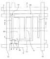
次に、本発明の液晶表示装置の実施形態について、図1、2の断面図及び平面図を参照して説明する。図2は、本発明の液晶表示装置のTFT基板を液晶側から眺めたときの1画素の平面図であり、図1は、図2の切断線X-X'に沿った断面図である。まず、ガラス等からなる透明性絶縁基板1の上に200〜500nmの膜厚の金属膜(例えばCr、Al、Ta、または、これらの合金)が被着されてパターニングされ、走査配線3およびそれにつながるゲート電極2、共通配線4が同時に形成される。その後、全面にゲート絶縁膜6(例えば、400〜600nmの膜厚のSiNx等)形成される。続いて、ゲート絶縁膜6の上に半導体アイランド7(例えば、アモルファスシリコンやポリシリコン)を形成し、さらにこの上に200〜500nmの膜厚の金属膜(例えばCr、Al、Ta、または、これらの合金)を被着してパターニングし、信号配線10、ソース/ドレイン電極8、9、およびドレイン電極9につながる第1の画素電極11(下層画素電極)が形成される。このとき、第1の画素電極11は、図1に示されるように、後の工程で形成される共通電極5と平行な電極部以外に共通配線4と重畳して配置される容量電極部22を有する構成であり、共通配線4及び容量電極部22は補助容量を構成する。このように、下層画素電極は容量蓄積電極としての働きを行う。次に、半導体アイランド7、ソース・ドレイン電極8、9、信号配線10、第1の画素電極11を覆って例えば200〜400nmの膜厚のSiNx等の第1の層間絶縁膜12が堆積され、続いて共通配線4及びソース・ドレイン電極9上に位置する絶縁膜の一部を開口して共通電極用コンタクトホール31及び画素電極用コンタクトホール32を形成する。次に、第1の層間絶縁膜12の上に60〜120nmの膜厚の金属膜(例えばCr、Al、Ta、または、これらの合金)を被着、パターニングして、共通電極用コンタクトホール31を通して共通配線4に接続される共通電極5、画素電極用コンタクトホール32を通してドレイン電極9に接続される第2の画素電極25(上層画素電極)を形成する。このとき、共通電極5及び第2の画素電極25は、互いに平行する電極部分を有するように形成され、また共通電極5は第1の画素電極11とも互いに平行する電極部分を有する。また、第2の画素電極25(上層画素電極)は下層画素電極11とは重ならないように設けている。さらに、共通電極5及び第2の画素電極25を覆って例えば600〜800nmの膜厚のSiNx等の第2の層間絶縁膜26が堆積される。続いて、配向膜材料を80〜120nmの膜厚に塗布してラビングすると配向膜13が形成される。このようにしてTFT基板100が完成する。一方、TFT基板100に対向配置される対向基板200は概略次のように形成される。まず、透明性絶縁基板51の上にTFT基板100の画素を区画する領域及び半導体アイランド7に対応するように遮光膜52が形成され、その上を絶縁膜53、配向膜54が覆うようにして形成される。このようにして得られたTFT基板100及び対向基板200の間に液晶27が充填され、液晶表示装置が完成する。図1では簡略化のために偏光板等は省略している。このように、画素電極25や共通電極5を、大きな電流容量を必要とする信号線10や共通配線4とは別の層に設けることにより、その金属膜厚を信号線や共通配線と独立に設定できるようにした。その結果、画素電極および共通電極の金属膜厚を信号線や共通配線よりも薄くできるようになったので、その上の上層絶縁膜26表面の凹凸を減少させることができた。すなわち、横方向の電界を生じさせる一方の組の共通電極5及び第2の画素電極25は、従来の200〜500nmの膜厚の金属膜よりもはるかに薄い60〜120nmの膜厚の金属膜からなり、それらの下にも段差を生じさせる配線・電極が配置されていないため、その上を覆う第2の層間絶縁膜26に従来よりもはるかに小さい段差しか生じない。また、横方向の電界を生じさせるもう他方の組の共通電極5及び第1の画素電極11も、第1の画素電極11の膜厚は200〜500nmと厚いものの、その上を第1の層間絶縁膜12及び第2の層間絶縁膜26で覆う構成であるために、配向膜13下の段差は大幅に小さくなっている。従って、第2の層間絶縁膜26の上に塗布される配向膜材料が平坦性良く形成され、その後に続く配向膜材料に対するラビングが配向膜材料全体に均一に行われ、均一な配向膜13が形成される。このように均一な配向膜を有する液晶表示装置は、特にモノクロ表示の液晶表示装置においてその効果が顕著であり、白輝度を黒輝度で割って得られるコントラストが、図3、4に示した構造の液晶表示装置に比べて約1.5倍に向上した。本実施形態では第2の層間絶縁膜の膜厚を第1の層間絶縁膜よりも厚く形成したが、液晶表示装置において許されるコントラストの範囲において薄くすることも可能であり、また第2の層間絶縁膜を無機膜ではなく有機膜で形成して膜厚を第1の層間絶縁膜よりも薄くすることも可能である。上述の形態では、蓄積電極を設ける例を示したが、蓄積電極を設けない場合も同様にして、信号線や共通配線とは別の層に画素電極および共通電極を設ければ、同様の効果をうることは明らかである。
【0007】
【発明の効果】
上述のように、本発明の液晶表示装置によれば、横方向電界を発生させる主要な電極部分を他の電極・配線が形成される層と別の層にして他の電極・配線よりも薄く形成されるので配向膜の下地膜の平坦性が大幅に改善され、下地膜の上に塗布される配向膜材料も平坦性良く形成され、従って配向膜材料に対するラビングが基板全面に渡って均一に行われる。これにより、均一にラビングされた配向膜が形成され、コントラストが大幅に向上した液晶表示装置が得られる。
【図面の簡単な説明】
【図1】本発明の実施形態の液晶表示装置の断面図であり、図2のX−X‘に沿った断面図である。
【図2】本発明の実施形態の液晶表示装置の平面図である。
【図3】従来の液晶表示装置の断面図であり、図4のX−X‘に沿った断面図である。
【図4】従来の液晶表示装置の平面図である。
【符号の説明】
1、51、101、151 透明絶縁性基板
2、102 ゲート電極
3、103走査配線
4、104 共通配線
5、105 共通電極
6、106 ゲート絶縁膜
7、107 半導体アイランド
8、108 ソース電極
9、109 ドレイン電極
10、110 信号配線
11 第1の画素電極
12 第1の層間絶縁膜
13、54、113、154 配向膜
22 容量電極部
25 第2の画素電極
26 第2の層間絶縁膜
27、127 液晶
31 共通電極用コンタクトホール
32 画素電極用コンタクトホール
52、152 遮光膜
53、153 絶縁膜
100、300 TFT基板
111 画素電極
200、400 対向基板[0001]
TECHNICAL FIELD OF THE INVENTION
The present invention relates to a liquid crystal display device that drives liquid crystal by a lateral electric field method in which an electric field substantially parallel to a substrate is applied between a pixel electrode and a common electrode.
[0002]
[Prior art]
An active matrix type liquid crystal display device using an active element such as a thin film transistor (TFT) is widely used as a display terminal because of its features of being thin, lightweight, and high image quality. In this type of liquid crystal display device, a liquid crystal is sandwiched between a TFT (active matrix) substrate having a thin film transistor and an opposing substrate disposed opposite thereto, and a pixel electrode and a common electrode formed on the TFT substrate are formed. A voltage is applied during this period to generate an electric field to drive and control the liquid crystal. As a result, an image is formed by modulating and emitting incident light. In the horizontal electric field method, since the liquid crystal is controlled by an electric field applied in a horizontal direction when viewed from the line of sight, the viewing angle can be widened. Here, the structure of the TFT substrate usually has a sectional view and a plan view as shown in FIGS. FIG. 4 is a plan view of one pixel when a TFT substrate of a conventional liquid crystal display device is viewed from the liquid crystal side, and FIG. 3 is a cross-sectional view taken along a cutting line XX ′ of FIG. That is, a
[0003]
[Problems to be solved by the invention]
Here, the
[0004]
[Means for Solving the Problems]
A liquid crystal display device having a basic structure according to the present inventionincludes a TFT substrate having a thin film transistor mounted on aninsulating substrate, driving the thin film transistor to generate an electric field parallel to the surface of the insulating substrate, and disposed to face the TFT substrate. A liquid crystal display device comprising: a counter substrate; a TFT substrate; and a liquid crystal filled in the counter substrate, wherein the TFT substrate includes the insulating substrate and a gate electrode formed on the insulating substrate. A wiring and a common wiring, a gate insulating film on the insulating substrate covering the scanning wiring and the common wiring, and a first pixel electrode formed on the gate insulating film and connected to a drain electrode of the thin film transistor A first interlayer insulating film on the gate insulating film and covering the first pixel electrode; and a common electrode and a second electrode formed on the first interlayer insulating film. A pixel electrode, and a second interlayer insulating film on the first interlayer insulating film and covering the common electrode and the second pixel electrode, wherein the common electrode and the second pixel electrode are And an electrode connected to the common wiring and the first pixel electrode and parallel to the first pixel electrode, respectively, and these parallel electrodes do not overlap with each other .
[0005]
In the liquid crystal display device having the basic structure of the present invention,the second pixel electrode and the common electrode are formed to be thinner than the first pixel electrode, and the second pixel electrode and the common electrode are Are connected to the drain electrode and the common wiring via contact holes, respectively. The first pixel electrode and the common wiring may include an overlapping portion to form an auxiliary capacitance. Further, the common electrode and the second pixel electrode may be light-shielding metal films.
[0006]
BEST MODE FOR CARRYING OUT THE INVENTION
Next, an embodiment of the liquid crystal display device of the present invention will be described with reference to the cross-sectional views and plan views of FIGS. FIG. 2 is a plan view of one pixel when the TFT substrate of the liquid crystal display device of the present invention is viewed from the liquid crystal side. FIG. 1 is a cross-sectional view taken along the line XX ′ of FIG. First, 200 to 500 nm of the film thickness of the metal film on the transparent insulating substrate 1 made of glass or the like (e.g. Cr, Al, Ta, or alloys thereof) are patterned is deposited, the
[0007]
【The invention's effect】
As described above, according to the liquid crystal display device of the present invention, a main electrode portion for generating a lateral electric field is formed in a layer different from a layer on which other electrodes and wirings are formed, and is thinner than other electrodes and wirings. Because of this, the flatness of the base film of the alignment film is greatly improved, and the alignment film material applied on the base film is also formed with good flatness, so that rubbing of the alignment film material is uniform over the entire surface of the substrate. Done. As a result, a uniformly rubbed alignment film is formed, and a liquid crystal display device with significantly improved contrast is obtained.
[Brief description of the drawings]
FIG. 1 is a cross-sectional view of a liquid crystal display device according to an embodiment of the present invention, which is a cross-sectional view along XX ′ of FIG.
FIG. 2 is a plan view of the liquid crystal display device according to the embodiment of the present invention.
FIG. 3 is a cross-sectional view of the conventional liquid crystal display device, which is a cross-sectional view along XX ′ of FIG.
FIG. 4 is a plan view of a conventional liquid crystal display device.
[Explanation of symbols]
1, 51, 101, 151 Transparent insulating
8,108 source electrode
9, 109 a
25
Claims (8)
Translated fromJapanesePriority Applications (5)
| Application Number | Priority Date | Filing Date | Title |
|---|---|---|---|
| JP2002021184AJP3586674B2 (en) | 2002-01-30 | 2002-01-30 | Liquid crystal display |
| TW092101327ATWI225569B (en) | 2002-01-30 | 2003-01-22 | Lateral electric field liquid crystal display device |
| US10/353,023US6888601B2 (en) | 2002-01-30 | 2003-01-29 | Lateral electric field liquid crystal display device |
| KR10-2003-0005758AKR100510564B1 (en) | 2002-01-30 | 2003-01-29 | Lateral electric field liquid crystal display device |
| CNB031031285ACN1252526C (en) | 2002-01-30 | 2003-01-30 | Transverse electric field liquid crystal display |
Applications Claiming Priority (1)
| Application Number | Priority Date | Filing Date | Title |
|---|---|---|---|
| JP2002021184AJP3586674B2 (en) | 2002-01-30 | 2002-01-30 | Liquid crystal display |
Publications (2)
| Publication Number | Publication Date |
|---|---|
| JP2003222903A JP2003222903A (en) | 2003-08-08 |
| JP3586674B2true JP3586674B2 (en) | 2004-11-10 |
Family
ID=27606306
Family Applications (1)
| Application Number | Title | Priority Date | Filing Date |
|---|---|---|---|
| JP2002021184AExpired - LifetimeJP3586674B2 (en) | 2002-01-30 | 2002-01-30 | Liquid crystal display |
Country Status (5)
| Country | Link |
|---|---|
| US (1) | US6888601B2 (en) |
| JP (1) | JP3586674B2 (en) |
| KR (1) | KR100510564B1 (en) |
| CN (1) | CN1252526C (en) |
| TW (1) | TWI225569B (en) |
Families Citing this family (13)
| Publication number | Priority date | Publication date | Assignee | Title |
|---|---|---|---|---|
| JP2003228081A (en) | 2002-01-31 | 2003-08-15 | Nec Corp | Liquid crystal display device and manufacturing method therefor |
| US7916254B2 (en)* | 2003-10-27 | 2011-03-29 | Hitachi Displays, Ltd. | Liquid crystal display apparatus for performing alignment process by irradiating light |
| KR101046923B1 (en)* | 2004-02-02 | 2011-07-06 | 삼성전자주식회사 | Thin film transistor array panel and liquid crystal display including the same |
| KR20050091291A (en)* | 2004-03-11 | 2005-09-15 | 엘지.필립스 엘시디 주식회사 | In plane switching mode liquid crystal display device and method of fabricating thereof |
| KR20060077870A (en)* | 2004-12-31 | 2006-07-05 | 엘지.필립스 엘시디 주식회사 | Transverse electric field liquid crystal display device |
| CN100417995C (en)* | 2005-10-10 | 2008-09-10 | 友达光电股份有限公司 | Wire substrate of liquid crystal display and manufacturing method thereof |
| US20070133031A1 (en)* | 2005-12-08 | 2007-06-14 | Canon Kabushiki Kaisha | Image processing apparatus and image processing method |
| EP1843194A1 (en)* | 2006-04-06 | 2007-10-10 | Semiconductor Energy Laboratory Co., Ltd. | Liquid crystal display device, semiconductor device, and electronic appliance |
| JP2008090279A (en)* | 2006-09-04 | 2008-04-17 | Epson Imaging Devices Corp | Liquid crystal display and electronic apparatus |
| JP2008242262A (en)* | 2007-03-28 | 2008-10-09 | Tpo Displays Corp | Substrate of liquid crystal display device, and method of manufacturing the same |
| KR101291716B1 (en)* | 2009-12-11 | 2013-07-31 | 엘지디스플레이 주식회사 | Liquid crystal display device for liquid crystal modes requiring high drive voltag |
| KR20120077818A (en)* | 2010-12-31 | 2012-07-10 | 삼성전자주식회사 | Display substrate and method of manufacturing the same |
| CN103018979B (en)* | 2012-12-21 | 2015-06-17 | 昆山龙腾光电有限公司 | Blue phase liquid crystal display device |
Family Cites Families (12)
| Publication number | Priority date | Publication date | Assignee | Title |
|---|---|---|---|---|
| EP0588568B1 (en)* | 1992-09-18 | 2002-12-18 | Hitachi, Ltd. | A liquid crystal display device |
| JP2701698B2 (en)* | 1993-07-20 | 1998-01-21 | 株式会社日立製作所 | Liquid crystal display |
| US6049369A (en)* | 1995-09-11 | 2000-04-11 | Hitachi, Ltd. | Parallel-field TFT LCD having reference electrodes and a conductive layer |
| JP3597305B2 (en)* | 1996-03-05 | 2004-12-08 | 株式会社半導体エネルギー研究所 | Liquid crystal display device and manufacturing method thereof |
| JP3788649B2 (en)* | 1996-11-22 | 2006-06-21 | 株式会社半導体エネルギー研究所 | Liquid crystal display |
| JP4036498B2 (en)* | 1997-03-21 | 2008-01-23 | 松下電器産業株式会社 | Active matrix liquid crystal display device |
| WO1998047044A1 (en)* | 1997-04-11 | 1998-10-22 | Hitachi, Ltd. | Liquid crystal display device |
| KR100477130B1 (en) | 1997-09-25 | 2005-08-29 | 삼성전자주식회사 | Thin Film Transistor Board and Manufacturing Method of Flat Drive Liquid Crystal Display |
| JP3099816B2 (en)* | 1998-08-12 | 2000-10-16 | 日本電気株式会社 | Active matrix type liquid crystal display |
| KR100303440B1 (en) | 1998-11-02 | 2002-10-25 | 삼성전자 주식회사 | Liquid crystal display of in-plane switching mode |
| JP3577625B2 (en)* | 1998-11-26 | 2004-10-13 | 株式会社アドバンスト・ディスプレイ | Manufacturing method of liquid crystal display device |
| KR20050061610A (en)* | 1999-06-11 | 2005-06-22 | 마쯔시다덴기산교 가부시키가이샤 | Liquid crystal display |
- 2002
- 2002-01-30JPJP2002021184Apatent/JP3586674B2/ennot_activeExpired - Lifetime
- 2003
- 2003-01-22TWTW092101327Apatent/TWI225569B/ennot_activeIP Right Cessation
- 2003-01-29USUS10/353,023patent/US6888601B2/ennot_activeExpired - Lifetime
- 2003-01-29KRKR10-2003-0005758Apatent/KR100510564B1/ennot_activeExpired - Fee Related
- 2003-01-30CNCNB031031285Apatent/CN1252526C/ennot_activeExpired - Lifetime
Also Published As
| Publication number | Publication date |
|---|---|
| TWI225569B (en) | 2004-12-21 |
| US20030142259A1 (en) | 2003-07-31 |
| CN1252526C (en) | 2006-04-19 |
| US6888601B2 (en) | 2005-05-03 |
| KR20030065396A (en) | 2003-08-06 |
| CN1435719A (en) | 2003-08-13 |
| JP2003222903A (en) | 2003-08-08 |
| TW200302385A (en) | 2003-08-01 |
| KR100510564B1 (en) | 2005-08-26 |
Similar Documents
| Publication | Publication Date | Title |
|---|---|---|
| JP3708637B2 (en) | Liquid crystal display device | |
| JP3240858B2 (en) | Color display | |
| JP3134866B2 (en) | Liquid crystal display device and manufacturing method thereof | |
| US7671931B2 (en) | Liquid crystal display device and method of fabricating the same | |
| JP2001144301A5 (en) | ||
| JPH01156725A (en) | Display device | |
| JP3586674B2 (en) | Liquid crystal display | |
| JP2007165824A (en) | Thin film transistor array substrate and manufacturing method thereof | |
| JP2008268841A (en) | Liquid crystal device, method for manufacturing liquid crystal device, and electronic apparatus | |
| US20040135939A1 (en) | Liquid crystal display device with light shielding structure and method for forming the same | |
| TWI283380B (en) | Electro-optical device, method of manufacturing electro-optical device | |
| JP3127619B2 (en) | Active matrix substrate | |
| US20100157225A1 (en) | Liquid crystal display unit and electronic device | |
| JP6960807B2 (en) | Display device and its manufacturing method | |
| KR101182311B1 (en) | Liquid crystal display panel and fabricating method thereof | |
| JPH04326329A (en) | Liquid crystal display device and its manufacturing method | |
| US6850299B2 (en) | Liquid crystal display device | |
| JP2000284723A (en) | Display device | |
| KR20070069054A (en) | Electro-optical device, manufacturing method thereof, and electronic device | |
| JPH10268356A (en) | Liquid crystal display | |
| WO2018168767A1 (en) | Liquid crystal display device | |
| JP2002296619A (en) | Active matrix type display device | |
| US7839463B2 (en) | Thin film diode panel and manufacturing method of the same | |
| JP2002297058A (en) | Active matrix type display device | |
| JPH06326310A (en) | Active matrix type display device |
Legal Events
| Date | Code | Title | Description |
|---|---|---|---|
| A977 | Report on retrieval | Free format text:JAPANESE INTERMEDIATE CODE: A971007 Effective date:20031212 | |
| A131 | Notification of reasons for refusal | Free format text:JAPANESE INTERMEDIATE CODE: A131 Effective date:20031216 | |
| A521 | Request for written amendment filed | Free format text:JAPANESE INTERMEDIATE CODE: A523 Effective date:20040210 | |
| TRDD | Decision of grant or rejection written | ||
| A01 | Written decision to grant a patent or to grant a registration (utility model) | Free format text:JAPANESE INTERMEDIATE CODE: A01 Effective date:20040720 | |
| A61 | First payment of annual fees (during grant procedure) | Free format text:JAPANESE INTERMEDIATE CODE: A61 Effective date:20040809 | |
| R150 | Certificate of patent or registration of utility model | Ref document number:3586674 Country of ref document:JP Free format text:JAPANESE INTERMEDIATE CODE: R150 Free format text:JAPANESE INTERMEDIATE CODE: R150 | |
| FPAY | Renewal fee payment (event date is renewal date of database) | Free format text:PAYMENT UNTIL: 20070813 Year of fee payment:3 | |
| FPAY | Renewal fee payment (event date is renewal date of database) | Free format text:PAYMENT UNTIL: 20080813 Year of fee payment:4 | |
| FPAY | Renewal fee payment (event date is renewal date of database) | Free format text:PAYMENT UNTIL: 20080813 Year of fee payment:4 | |
| FPAY | Renewal fee payment (event date is renewal date of database) | Free format text:PAYMENT UNTIL: 20090813 Year of fee payment:5 | |
| FPAY | Renewal fee payment (event date is renewal date of database) | Free format text:PAYMENT UNTIL: 20090813 Year of fee payment:5 | |
| FPAY | Renewal fee payment (event date is renewal date of database) | Free format text:PAYMENT UNTIL: 20100813 Year of fee payment:6 | |
| FPAY | Renewal fee payment (event date is renewal date of database) | Free format text:PAYMENT UNTIL: 20110813 Year of fee payment:7 | |
| FPAY | Renewal fee payment (event date is renewal date of database) | Free format text:PAYMENT UNTIL: 20110813 Year of fee payment:7 | |
| FPAY | Renewal fee payment (event date is renewal date of database) | Free format text:PAYMENT UNTIL: 20120813 Year of fee payment:8 | |
| FPAY | Renewal fee payment (event date is renewal date of database) | Free format text:PAYMENT UNTIL: 20120813 Year of fee payment:8 | |
| S533 | Written request for registration of change of name | Free format text:JAPANESE INTERMEDIATE CODE: R313533 | |
| FPAY | Renewal fee payment (event date is renewal date of database) | Free format text:PAYMENT UNTIL: 20120813 Year of fee payment:8 | |
| R350 | Written notification of registration of transfer | Free format text:JAPANESE INTERMEDIATE CODE: R350 | |
| FPAY | Renewal fee payment (event date is renewal date of database) | Free format text:PAYMENT UNTIL: 20130813 Year of fee payment:9 | |
| R250 | Receipt of annual fees | Free format text:JAPANESE INTERMEDIATE CODE: R250 | |
| R250 | Receipt of annual fees | Free format text:JAPANESE INTERMEDIATE CODE: R250 | |
| R250 | Receipt of annual fees | Free format text:JAPANESE INTERMEDIATE CODE: R250 | |
| R250 | Receipt of annual fees | Free format text:JAPANESE INTERMEDIATE CODE: R250 | |
| R250 | Receipt of annual fees | Free format text:JAPANESE INTERMEDIATE CODE: R250 | |
| EXPY | Cancellation because of completion of term |