JP3586119B2 - Head substrate, inkjet head, inkjet printer - Google Patents
Head substrate, inkjet head, inkjet printerDownload PDFInfo
- Publication number
- JP3586119B2 JP3586119B2JP30617898AJP30617898AJP3586119B2JP 3586119 B2JP3586119 B2JP 3586119B2JP 30617898 AJP30617898 AJP 30617898AJP 30617898 AJP30617898 AJP 30617898AJP 3586119 B2JP3586119 B2JP 3586119B2
- Authority
- JP
- Japan
- Prior art keywords
- ink
- head
- fuse array
- fuse
- logic circuit
- Prior art date
- Legal status (The legal status is an assumption and is not a legal conclusion. Google has not performed a legal analysis and makes no representation as to the accuracy of the status listed.)
- Expired - Fee Related
Links
Images


Classifications
- B—PERFORMING OPERATIONS; TRANSPORTING
- B41—PRINTING; LINING MACHINES; TYPEWRITERS; STAMPS
- B41J—TYPEWRITERS; SELECTIVE PRINTING MECHANISMS, i.e. MECHANISMS PRINTING OTHERWISE THAN FROM A FORME; CORRECTION OF TYPOGRAPHICAL ERRORS
- B41J2/00—Typewriters or selective printing mechanisms characterised by the printing or marking process for which they are designed
- B41J2/005—Typewriters or selective printing mechanisms characterised by the printing or marking process for which they are designed characterised by bringing liquid or particles selectively into contact with a printing material
- B41J2/01—Ink jet
- B41J2/135—Nozzles
- B41J2/14—Structure thereof only for on-demand ink jet heads
- B41J2/14016—Structure of bubble jet print heads
- B41J2/14072—Electrical connections, e.g. details on electrodes, connecting the chip to the outside...
- B—PERFORMING OPERATIONS; TRANSPORTING
- B41—PRINTING; LINING MACHINES; TYPEWRITERS; STAMPS
- B41J—TYPEWRITERS; SELECTIVE PRINTING MECHANISMS, i.e. MECHANISMS PRINTING OTHERWISE THAN FROM A FORME; CORRECTION OF TYPOGRAPHICAL ERRORS
- B41J2202/00—Embodiments of or processes related to ink-jet or thermal heads
- B41J2202/01—Embodiments of or processes related to ink-jet heads
- B41J2202/17—Readable information on the head
Landscapes
- Particle Formation And Scattering Control In Inkjet Printers (AREA)
- Ink Jet (AREA)
Description
Translated fromJapanese【0001】
【発明の属する技術分野】
本発明は、一個のベース基板に各種層膜が積層されているヘッド基体、このヘッド基体を利用したインクジェットヘッド、このインクジェットヘッドを利用したインクジェットプリンタ、に関する。
【0002】
【従来の技術】
従来、各種方式の画像形成装置が実施されており、例えば、レーザプリンタやインクジェットプリンタがある。インクジェットプリンタは、記録媒体にインク滴を吐出して画像を形成するもので、インク滴を吐出する手法としてはバブルジェット方式と呼称される電気熱変換方式がある。
【0003】
電気熱変換方式のインクジェットプリンタは、ノズルや供給路やインク溜からなるインク保持部にインク液を保持した状態で、ノズルの発熱素子でインク液を加熱して気泡を発生させ、この気泡の圧力でインクを押圧してノズルからインク滴を吐出する。
【0004】
一般的なインクジェットプリンタでは、上述のような構造のインクジェットヘッドがキャリア機構により主走査方向に移動自在に支持されており、このインクジェットヘッドと対向する位置を記録媒体である印刷用紙が用紙搬送機構により副走査方向に順次搬送される。
【0005】
これでインクジェットヘッドがインク滴を吐出する位置と印刷用紙の表面とが主走査方向と副走査方向とに相対移動するので、印刷データに対応してインクジェットヘッドがインク滴を印刷用紙の表面に吐出することにより、この印刷用紙の表面には付着したインクでドットマトリクスの画像が形成されることになる。
【0006】
インクジェットヘッドは、例えば、ヘッド基体とカバー部材とを組み合わせた構造からなり、カバー部材は、隔壁を形成する層膜とカバー基板からなる。ヘッド基体は、一個のベース基板を具備しており、このベース基板の表面に各種の層膜でインク吐出機構などが形成されている。
【0007】
このインク吐出機構は、電気熱変換方式の場合はヒータ素子からなり、電気機械変換方式の場合はピエゾ素子からなる。このようなヘッド基体において、インク吐出機構を駆動するドライバ回路や、このドライバ回路に印刷データを供給するデータ入力部も、ベース基板の表面に各種の層膜で形成することが現在では一般的である。
【0008】
さらに、現在ではインクジェットヘッドに、自身のID(Identity)コードやインク吐出機構の駆動特性を読出自在にデータ保持させるため、ヘッド基体にROM(Read Only Memory)を搭載することが提案されている。例えば、インクジェットヘッドにEEPROM(Electrically Erasable Programmable ROM)を搭載することが、特開平3−126560号公報に開示されている。
【0009】
しかし、上記公報のインクジェットヘッドでは、EEPROMをヘッド基体とは別個に搭載しているので、装置の構造が複雑で生産性も良好でなく、装置の小型軽量化も阻害されている。特に、記録データが大容量の場合は既存のROMチップは有用であるが、記録データが大容量でない場合にはROMチップはコスト的に不利なことがある。
【0010】
そこで、特開平8−177732号公報、USP5504507、USP5363134等には、インクジェットヘッドのヘッド基体のベース基板に、ヒューズアレイからなるROMをインク吐出機構などの層膜とともに形成することが開示されている。
【0011】
この場合、ヘッド基体を製造するためにベース基板にインク吐出機構などの層膜を形成するとき、ROMとなるヒューズアレイを同時に形成することができる。例えば、このヒューズアレイを同時に形成したロジック回路の制御により選択的に溶断すれば、その溶断の有無により二値データを保持させることができる。
【0012】
このため、上述のようなヘッド基体を利用したインクジェットヘッドでは、ヘッド基体とは別個にROMチップを用意する必要がなく、各種データを読出自在に保持できる構造を簡略化して生産性を向上させることができ、その小型軽量化も実現することができる。
【0013】
【発明が解決しようとする課題】
上述したヘッド基体では、インクジェットプリンタの各種データをヒューズアレイにより読出自在に保持することができ、このヒューズアレイをベース基板に各種層膜とともに形成することができる。一般的なインクジェットヘッドでは、ヘッド基体の表面の大部分がインク保持部で占有されているので、例えば、図9(a)に示すように、インク溜と重複する位置にヒューズアレイが形成される。
【0014】
同図のインクジェットヘッド100では、ヘッド基体101は、ベース基板102の表面に、ヒューズアレイのヒューズ素子103、層間絶縁膜104、ヒューズ電極105、保護膜106等が所定形状で適宜積層されており、この保護膜106の表面にカバー部材の隔壁などで(図示せず)インク溜107が形成されている。
【0015】
つまり、ヒューズ素子103に保護膜106を介してインク液108が対向しているが、ヒューズアレイは多数のヒューズ素子103の選択的な溶断により各種データを保持するので、必然的にデータ記憶の実行時には多大な熱量を発生することになる。
【0016】
このため、上述のようなインクジェットヘッド100でヒューズアレイに各種データを保持させるためにヒューズ素子103を溶断するとき、同図(b)に示すように、その局所的な発熱のために上層の層間絶縁膜104や保護膜106にクラックが発生することがある。
【0017】
この場合、インク溜107のインク液108がクラックによりヒューズ素子103の位置まで浸透するので、例えば、溶断したヒューズ素子103がインク液108により短絡されたり、インク液108によりヒューズ素子103やヒューズ電極105が腐食されることが発生する。
【0018】
特に、ヒューズ素子103の溶断やデータ読書を動作制御するロジック回路をヒューズアレイの周辺に形成した場合、このロジック回路もクラックから浸透したインク液108に汚染されることになり、ヒューズアレイやロジック回路に誤動作が発生することになる。
【0019】
このような課題を解決するため、ヒューズアレイのデータ記憶が完了してから保護膜106を積層することも想定できるが、例えば、インク吐出機構の動作特性をヒューズアレイにデータ記憶させる場合、インクジェットヘッド100を完成して動作させてからヒューズアレイを溶断する必要がある。
【0020】
本発明は上述のような課題に鑑みてなされたものであり、ヒューズアレイを選択的に溶断させてもインク液による障害が発生しないヘッド基体、このヘッド基体を利用したインクジェットヘッド、このインクジェットヘッドを利用したインクジェットプリンタ、を提供することを目的とする。
【0021】
【課題を解決するための手段】
本発明の第一のヘッド基体は、インク保持部に保持しているインク液をデータ入力部に外部入力される印刷データに対応してインク吐出機構により吐出させるインクジェットヘッドのヘッド基体であって、
前記インク保持部が配置される表面の位置が特定されている一個のベース基板と、選択的な溶断により各種データを読出自在に記憶するヒューズアレイと、前記ヒューズアレイの選択的な溶断やデータ読出を動作制御するヒューズロジック回路と、を具備しており、前記ベース基板の表面と直交する方向で前記インク保持部とは重複しない位置に前記ヒューズアレイと前記ヒューズロジック回路とが配置されている。
【0022】
従って、本発明のヘッド基体を利用してインクジェットヘッドを形成すると、このインクジェットヘッドでは、ヘッド基体の表面に形成されるインク保持部によりインク液を保持することができ、このインク液をヘッド基体のインク吐出機構によりインク滴として吐出することができる。さらに、この動作特性などの各種データをヒューズロジック回路によりヒューズアレイに記憶させることができ、このヒューズアレイの記憶データをヒューズロジック回路により自在に読み出すことができる。ただし、ベース基板の表面と直交する方向でヒューズアレイおよびヒューズロジック回路の位置がインク保持部と重複しないので、例えば、ヒューズアレイの上層に溶断の熱量によりクラックが発生しても、このクラックがインク保持部の位置に発生してインク液が浸透することがない。
【0023】
上述のようなヘッド基体において、前記インク吐出機構が前記インク保持部下の位置で前記ベース基板に形成されてインク液を加熱により発泡させるヒータ素子を具備していることも可能である。この場合、インク保持部下の位置でベース基板に形成されているヒータ素子がインク液を加熱により発泡させるので、これでインク吐出機構はインク液をインク滴として吐出させることになる。
【0024】
上述のようなヘッド基体において、少なくとも前記ヒータ素子と前記インク保持部との間隙に位置してインク液のキャビテーションの影響を防止する耐キャビテーション膜も具備しており、該耐キャビテーション膜が前記ベース基板の表面と直交する方向で前記ヒューズアレイおよび前記ヒューズロジック回路と重複する位置まで形成されていることも可能である。
【0025】
この場合、インク滴を吐出させるためにインク液を発泡させるとキャビテーションが発生するが、その影響は耐キャビテーション膜により防止されるのでヒータ素子などが損傷することがない。しかも、ベース基板の表面と直交する方向でヒューズアレイおよびヒューズロジック回路と重複する位置まで耐キャビテーション膜が形成されているので、例えば、ヒューズアレイの溶断により局所的な発熱が発生しても、この発熱の影響が耐キャビテーション膜により防止され、ヒューズアレイの溶断の熱量によるクラックが耐キャビテーション膜より上層まで発生することがない。
【0026】
本発明の第二のヘッド基体は、インク保持部に保持しているインク液をデータ入力部に外部入力される印刷データに対応してインク吐出機構により吐出させるインクジェットヘッドのヘッド基体であって、
前記インク保持部が配置される表面の位置が特定されている一個のベース基板と、前記インク吐出機構として前記インク保持部下の位置で前記ベース基板に形成されてインク液を加熱により発泡させるヒータ素子と、少なくとも前記ヒータ素子と前記インク保持部との間隙に位置してインク液のキャビテーションの影響を防止する耐キャビテーション膜と、選択的な溶断により各種データを読出自在に記憶するヒューズアレイと、前記ヒューズアレイの選択的な溶断やデータ読出を動作制御するヒューズロジック回路と、を具備しており、前記ベース基板の表面と直交する方向で前記ヒューズアレイおよび前記ヒューズロジック回路と重複する位置まで前記耐キャビテーション膜が形成されている。
【0027】
従って、本発明のヘッド基体を利用してインクジェットヘッドを形成すると、このインクジェットヘッドでは、ヘッド基体の表面に形成されるインク保持部によりインク液を保持することができ、このインク液をヘッド基体のヒータ素子により発泡させてインク滴を吐出させることができる。インク滴を吐出させるためにインク液を発泡させるとキャビテーションが発生するが、その影響は耐キャビテーション膜により防止されるのでヒータ素子などが損傷することもない。インク滴を吐出させる動作特性などの各種データをヒューズロジック回路によりヒューズアレイに記憶させることができ、このヒューズアレイの記憶データをヒューズロジック回路により自在に読み出すことができる。ただし、ベース基板の表面と直交する方向でヒューズアレイおよびヒューズロジック回路と重複する位置まで耐キャビテーション膜が形成されているので、例えば、ヒューズアレイの溶断により局所的な発熱が発生しても、この発熱の影響が耐キャビテーション膜により防止される。このため、ヒューズアレイの溶断の熱量によるクラックが耐キャビテーション膜より上層まで発生することがなく、クラックがインク保持部の位置に発生してインク液が浸透することがない。
【0028】
本発明の第三のヘッド基体は、インク保持部に保持しているインク液をデータ入力部に外部入力される印刷データに対応してインク吐出機構により吐出させるインクジェットヘッドのヘッド基体であって、
前記インク保持部が配置される表面の位置が特定されている一個のベース基板と、前記インク吐出機構として前記インク保持部下の位置で前記ベース基板に形成されてインク液を加熱により発泡させるヒータ素子と、少なくとも前記ヒータ素子と前記インク保持部との間隙に位置してインク液のキャビテーションの影響を防止する耐キャビテーション膜と、選択的な溶断により各種データを読出自在に記憶するヒューズアレイと、前記ヒューズアレイの選択的な溶断やデータ読出を動作制御するヒューズロジック回路と、を具備しており、前記ベース基板の表面と直交する方向で前記インク保持部と前記ヒューズアレイとが少なくとも一部は重複する位置に配置されており、前記インク保持部と前記ヒューズアレイとが重複する位置まで前記耐キャビテーション膜が形成されている。
【0029】
従って、本発明のヘッド基体を利用してインクジェットヘッドを形成すると、このインクジェットヘッドでは、ヘッド基体の表面に形成されるインク保持部によりインク液を保持することができ、このインク液をヘッド基体のヒータ素子により発泡させてインク滴を吐出させることができる。インク滴を吐出させるためにインク液を発泡させるとキャビテーションが発生するが、その影響は耐キャビテーション膜により防止されるのでヒータ素子などが損傷することもない。インク滴を吐出させる動作特性などの各種データをヒューズロジック回路によりヒューズアレイに記憶させることができ、このヒューズアレイの記憶データをヒューズロジック回路により自在に読み出すことができる。ただし、ベース基板の表面と直交する方向でインク保持部とヒューズアレイとが重複する位置まで耐キャビテーション膜が形成されているので、例えば、ヒューズアレイの溶断により局所的な発熱が発生しても、この発熱の影響が耐キャビテーション膜により防止される。このため、ヒューズアレイの溶断の熱量によるクラックが耐キャビテーション膜より上層まで発生することがなく、クラックがインク保持部の位置に発生してインク液が浸透することがない。
【0030】
上述のようなヘッド基体において、前記ヒューズアレイが前記ヒータ素子と同一の材料で形成されていることも可能である。この場合、インク吐出機構のヒータ素子とヒューズアレイとが同一の材料で形成されているので、ヘッド基体の製造においてヒューズアレイを形成するために新規の材料を追加する必要がない。
【0031】
上述のようなヘッド基体において、該ヒータ素子より下層にバリア層が形成されており、該バリア層と同一の材料で前記ヒューズアレイが形成されていることも可能である。この場合、インク吐出機構のヒータ素子より下層にバリア層が形成されているので、ヒータ素子の発熱により下層の金属層にヒロックが成長することがバリア層により防止される。このようなバリア層とヒューズアレイとが同一の材料で形成されているので、ヘッド基体の製造においてヒューズアレイを形成するために新規の材料を追加する必要がない。
【0032】
上述のようなヘッド基体において、各種の配線を具備して前記インク吐出機構の動作を制御する印刷ロジック回路も前記ベース基板に形成されており、該印刷ロジック回路の配線と同一の材料で前記ヒューズアレイが形成されていることも可能である。
【0033】
この場合、ベース基板に各種の配線などで形成されているロジック回路によりインク吐出機構の動作が制御されるので、これでインク吐出機構はインク液をインク滴として適正に吐出する。このようなロジック回路の配線とヒューズアレイとが同一の材料で形成されているので、ヘッド基体の製造においてヒューズアレイを形成するために新規の材料を追加する必要がない。
【0034】
上述のようなヘッド基体において、前記ヒューズアレイが前記ヒータ素子より下層の層膜からなることも可能である。この場合、インク吐出機構のヒータ素子より下層の層膜によりヒューズアレイが形成されているので、例えば、ヒューズアレイの溶断により局所的な発熱が発生して上層にクラックが発生しても、このクラックがインク保持部の位置まで到達しにくい。
【0035】
本発明のインクジェットヘッドは、本発明のヘッド基体と、該ヘッド基体の表面に設けられて前記インク保持部を形成するカバー部材と、を具備している。従って、本発明のインクジェットヘッドでは、カバー部材がヘッド基体の表面に設けられることでインク保持部が形成されるので、このインク保持部によりインク液が保持される。
【0036】
本発明のインクジェットプリンタは、本発明のインクジェットヘッドと、該インクジェットヘッドのインク保持部にインク液を供給するインク供給手段と、前記インクジェットヘッドのデータ入力部に印刷データをデータ入力するデータ入力手段と、前記インクジェットヘッドに対して記録媒体を相対移動させる相対移動手段と、前記インクジェットヘッドのヒューズアレイから前記ヒューズロジック回路により各種データを読み出すデータ読出手段と、を具備している。
【0037】
従って、本発明のインクジェットプリンタでは、インク供給手段がインクジェットヘッドのインク保持部にインク液を供給し、データ入力手段がインクジェットヘッドのデータ入力部に印刷データをデータ入力し、相対移動手段がインクジェットヘッドに対して記録媒体を相対移動させる。このため、インクジェットヘッドが印刷データに対応して記録媒体の表面にインク滴を吐出することになり、その位置が相対移動されるので付着したインク滴によりドットマトリクスの画像が形成される。データ読出手段がインクジェットヘッドのヒューズアレイからヒューズロジック回路により各種データを読み出すので、例えば、この読出データからインクジェットヘッドの動作特性を認識して駆動を調整するようなことができる。
【0038】
なお、本発明で云う各種手段は、その機能を実現するように形成されていれば良く、例えば、専用のハードウェア、適正な機能がプログラムにより付与されたコンピュータ、適正なプログラムによりコンピュータの内部に実現された機能、これらの組み合わせ、等を許容する。
【0039】
【発明の実施の形態】
本発明の実施の一形態を図1ないし図8を参照して以下に説明する。なお、図1は本実施の形態のインクジェットヘッドの内部レイアウトを示す模式的な平面図、図2はヘッド基体の回路構造を示すブロック図、図3はインクジェットヘッドの積層構造を示す模式的な縦断側面図、図4はインクジェットプリンタの外観を示す斜視図、図5はインクジェットプリンタの回路構造を示す模式的なブロック図、図6は各種信号の相互関係を示すタイムチャート、図7は一変形例のインクジェットヘッドの内部レイアウトを示す模式的な平面図、図8は一変形例のインクジェットヘッドの積層構造を示す模式的な縦断側面図、である。
【0040】
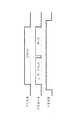
本実施の形態の画像処理システム200は、図5に示すように、中央制御装置であるホストコンピュータ210と画像形成装置であるインクジェットプリンタ300とを具備しており、このインクジェットプリンタ300とホストコンピュータ210とが通信ケーブル220で接続されている。
【0041】
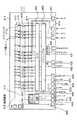
本実施の形態のインクジェットプリンタ300は、図4に示すように、インクジェットヘッド400を具備しており、このインクジェットヘッド400は、図3に示すように、ヘッド基体401とカバー部材402とを具備している。ヘッド基体401は、図1および図2に示すように、ベース基板410を具備しており、このベース基板410の表面に各種部材が層膜などで形成されている。
【0042】
本実施の形態のヘッド基体401では、ベース基板410の表面の前縁部に多数のヒータ素子411が形成されており、この多数のヒータ素子411によりインク吐出機構としてヒータ部412が形成されている。多数のヒータ素子411の各々の一端には多数のパワートランジスタ413のソース電極が個々に接続されており、これらのパワートランジスタ413によりドライバ回路414が形成されている。
【0043】
多数のヒータ素子411の他端と多数のパワートランジスタ413のドレイン電極とは一対の電源電極415,416に接続されており、多数のパワートランジスタ413のゲート電極には、印刷ロジック回路417の多数のアンドゲート418が個々に接続されている。ヒータ素子411は、例えば、窒化タンタル、タンタルアルミ、タンタル窒化珪素、等を材料とする層膜からなり、電源電極415,416からドライバ回路414を介して供給される駆動電力により発熱する。
【0044】
これら多数のアンドゲート418は複数の制御ブロックに分割されてマトリクス配線されているので、その制御ブロックごとに多数のアンドゲート418に複数のブロック電極419が接続されている。さらに、多数のアンドゲート418には、一個のパルス電極420と一個のラッチ回路421も接続されており、このラッチ回路421にはシフトレジスタ422が並列に接続されている。
【0045】
ラッチ回路421とシフトレジスタ422には、一個のリセット電極423が共通に接続されるとともに、各々固有のクロック電極424,425も個々に接続されており、シフトレジスタ422には、一個のデータ電極426も接続されている。
【0046】
ブロック電極419には、多数のヒータ素子411の複数の制御ブロックを選択する選択信号が入力され、パルス電極420には、ヒータ素子411の発熱時間を制御するヒートパルスが入力される。リセット電極423には、ラッチ回路421とシフトレジスタ422とをリセットするリセット信号が入力され、クロック電極424,425には、ラッチ回路421とシフトレジスタ422との動作周波数を決定するクロック信号が入力される。
【0047】
データ電極426には印刷データがシリアルに入力されるので、このシリアルな印刷データをシフトレジスタ422がパラレルに変換する。このパラレルな印刷データをラッチ回路421が一時保持してからアンドゲート418を介してドライバ回路414に供給するので、これで多数のヒータ素子411が印刷データに対応して発熱する。
【0048】
また、ベース基板410の表面には、温度センサや保温ヒータからなるセンサユニット430も形成されており、このセンサユニット430には一対のセンサ電極431が接続されている。また、一対の電源電極432,433も形成されており、これらの電源電極432,433が各部に接続されている。
【0049】
センサユニット430は、ベース基板410の保温加熱と温度測定とを実行し、センサ電極431は、センサユニット430の制御信号が入力される。電源電極432,433には、各部に供給される駆動電力が供給されるので、この駆動電力により印刷ロジック回路417などが動作する。
【0050】
そして、本実施の形態のヘッド基体401では、ベース基板410の表面に多数のヒューズ素子440からなるヒューズアレイ441も形成されており、このヒューズアレイ441を包囲するようにヒューズロジック回路442が形成されている。
【0051】
多数のヒューズ素子440は、一個のヒューズロジック回路442に多数のヒューズ電極443で個々に接続されており、ヒューズロジック回路442には、データ電極444、クロック電極445、イネーブル電極446、が接続されている。
【0052】
ヒューズアレイ441には、インクジェットヘッド400のIDコードやヒータ部412の動作特性などの各種データが出荷以前の時点でデータ記録されており、ヒューズロジック回路442は、ヒューズアレイ441のデータ記録やデータ読出を動作制御する。上述のようにヒューズアレイ441は、記憶するデータがIDコードや動作特性であるため、ここでは100ビット以下の記憶容量に形成されている。
【0053】
このため、図6に示すように、クロック電極445は、ヒューズロジック回路442の動作周波数を決定するクロック信号が入力され、イネーブル電極446は、ヒューズロジック回路442の動作を許可するイネーブル信号が入力される。データ電極444は、ヒューズロジック回路442がヒューズアレイ441に記憶させるデータが入力され、ヒューズロジック回路442がヒューズアレイ441から読み出すデータを出力する。
【0054】
なお、上述した各種の電極415…は、配線ラインと接続パッドとの総称であり、図1に示すように、多数の電極415…の接続パッドからなるデータ入力部であるパッド部447は、ヒータ部412とは反対となるベース基板410の後縁部に形成されている。
【0055】
つまり、本実施の形態のヘッド基体401は、同図に示すように、ベース基板410の表面の前縁部にヒータ部412が配置されており、その後方にドライバ部414と印刷ロジック回路417とヒューズロジック回路442とが順番に配列されており、ベース基板410の後縁部にパッド部447が配置されている。
【0056】
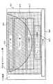
また、図3に示すように、ヒューズアレイ441のヒューズ素子440は、ベース基板410の表面に直接に積層されたポリシリコンの層膜からなり、このヒューズ素子440の上層には層間絶縁膜450が形成されている。この層間絶縁膜450の表面には、ヒューズ電極443、ヒータ素子411、ヒータ電極451、等が積層されており、ヒューズ電極443は層間絶縁膜450のスルーホールを介してヒューズ素子440に接続されている。
【0057】
さらに上層には保護膜452が積層されており、この保護膜452の表面の一部には耐キャビテーション膜453が積層されている。つまり、インクジェットヘッド400では、カバー部材402が封止部材460とカバー基板461からなり、このようなカバー部材402がヘッド基体401の表面に接合されることで、封止部材460を隔壁としてノズルや供給路やインク溜からなるインク保持部462がヘッド基体401の表面に形成されている。
【0058】
そこで、本実施の形態のインクジェットヘッド400のヘッド基体401では、図1および図3に示すように、その表面と直交する方向でインク保持部462と重複する位置に耐キャビテーション膜453が形成されており、この耐キャビテーション膜453およびインク保持部462と重複しない位置に、ヒューズアレイ441がヒューズロジック回路442とともに配置されている。
【0059】
なお、ヒータ/ヒューズロジック回路417,442は、各種の配線がポリシリコンの層膜で形成されているが、ヒューズアレイ441のヒューズ素子440も、各ロジック回路417,442の配線と同一のポリシリコンの層膜で形成されている。
【0060】
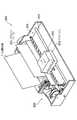
本実施の形態のインクジェットプリンタ300では、図4および図5に示すように、上述のような構造のインクジェットヘッド400がヘッド移動機構302のキャリッジ303に着脱自在に搭載されており、このキャリッジ303がガイドシャフト304等により主走査方向に移動自在に支持されているので、これでインクジェットヘッド400も主走査方向に移動自在に支持される。
【0061】
上述のように支持されたインクジェットヘッド400と対向する位置には、記録媒体である印刷用紙Pを保持して搬送するプラテンローラ305が配置されており、このプラテンローラ305等により印刷用紙Pを副走査方向に順次搬送する用紙搬送機構306が形成されている。
【0062】
ヘッド移動機構302と用紙搬送機構306とは一個の移動制御回路311に接続されており、この移動制御回路311はマイクロコンピュータ312に接続されている。このマイクロコンピュータ312がヘッド移動機構302と用紙搬送機構306とを統合制御するので、これでインクジェットヘッド400がインク滴を吐出する位置と印刷用紙Pの表面とを相対移動させる相対移動手段が形成されている。
【0063】
このマイクロコンピュータ312には、データ入力手段であるデータ入力回路313、データ読出手段であるデータ読出回路314、通信I/F315、等も接続されており、この通信I/F315に通信ケーブル220でホストコンピュータ210が接続されている。
【0064】
データ入力回路313は、キャリッジ303の接続コネクタ(図示せず)を介してインクジェットヘッド400の印刷ロジック回路417に接続されており、データ読出回路315は、キャリッジ303の接続コネクタを介してインクジェットヘッド400のヒューズロジック回路442に接続されている。
【0065】
データ入力回路313は、印刷データをインクジェットヘッド400の印刷ロジック回路417に供給し、データ読出回路314は、インクジェットヘッド400のヒューズロジック回路442からヒューズアレイ441の記憶データを読み出す。
【0066】
マイクロコンピュータ312は、上述のような各種回路311,313,314も統合制御し、例えば、ホストコンピュータ210から通信I/F315に入力される印刷データをデータ入力回路313に供給し、データ読出回路314がインクジェットヘッド400から読み出した記憶データを通信I/F315からホストコンピュータ210に出力する。
【0067】
また、本実施の形態のインクジェットプリンタ300は、インク供給手段であるインクタンク(図示せず)も具備しており、このインクタンクもキャリッジ303のソケット部材(図示せず)を介してインクジェットヘッド400のインク保持部462に配管されている。インクタンクにはインク液が事前に充填されており、このインク液をインクジェットヘッド400に供給する。
【0068】
上述のような構成において、本実施の形態の画像処理システム200では、例えば、ホストコンピュータ210がインクジェットプリンタ300に印刷データを供給するので、この印刷データをインクジェットプリンタ300が印刷用紙Pに印刷出力する。
【0069】
その場合、マイクロコンピュータ312の統合制御によりヘッド移動機構302がインクジェットヘッド400を主走査移動させるとともに、用紙搬送機構306が印刷用紙Pを副走査移動させ、これに同期してデータ入力回路313がインクジェットヘッド400に印刷データをデータ入力する。
【0070】
インクジェットヘッド400は、インクタンクから常時供給されるインク液をインク保持部462に保持しており、データ入力される印刷データに印刷ロジック回路417が多数のヒータ素子411を選択的に発熱駆動する。この多数のヒータ素子411の選択的な発熱によりインク保持部462のインク液が発泡してインク滴が吐出されるので、このインク滴が相対移動する印刷用紙Pの表面に付着してドットマトリクスの画像が形成される。
【0071】
本実施の形態の画像処理システム200では、インクジェットヘッド400がヒューズアレイ441を具備しているので、例えば、インクジェットヘッド400の製造を完了して出荷する以前の時点などに、IDコードやヒータ部412の動作特性などがヒューズアレイ441にデータ記録される。
【0072】
そこで、このようなデータ記録を完了してから出荷されたインクジェットヘッド400をインクジェットプリンタ300に装着すると、このインクジェットプリンタ300はデータ読出回路314によりインクジェットヘッド400のヒューズアレイ441から記憶データを読み出すことができる。
【0073】
このため、インクジェットプリンタ300は、例えば、インクジェットヘッド400のヒューズアレイ441から読み出したヒータ部412の動作特性に対応してヒータ部412に供給する駆動電力を調整するようなことや、インクジェットヘッド400のIDコードをホストコンピュータ210に通知するようなことができる。
【0074】
上述のようにヒータ部412の動作特性をヒューズアレイ441にデータ記録する場合、これは必然的にインクジェットヘッド400が完成してから実行されることになるが、図3に示すように、ヒューズ素子440の溶断の熱量により上層にクラックが発生することがある。
【0075】
しかし、本実施の形態のインクジェットヘッド400では、図1に示すように、ヒューズアレイ441とインク保持部462との位置が重複していないので、図3に示すように、ヒューズアレイ441の上層に溶断の熱量によりクラックが発生しても、このクラックがインク保持部462の位置に発生することがない。
【0076】
つまり、インク液がヒューズアレイ441やヒューズロジック回路442の位置まで浸透することがないので、溶断したヒューズ素子440がインク液により短絡してヒューズロジック回路442のデータ読出に誤動作が発生することがなく、インク液によりヒューズアレイ441やヒューズロジック回路442が腐食されることもない。
【0077】
なお、インク保持部462のインク液がヘッド基体401と封止部材460との間隙に浸透すると、このインク液がクラックからヒューズアレイ441やヒューズロジック回路442の位置まで浸透することも想定できるが、これはヘッド基体401とカバー部材402との接合の精度の問題で実際には無視することができる。
【0078】
特に、本実施の形態のインクジェットヘッド400では、積層構造においてヒューズアレイ441がヒータ素子411より下層の層膜からなるので、ヒューズアレイ441の溶断により上層にクラックが発生しても、このクラックがインク保持部462と同一の高さまで到達しにくく、インク液がヒューズアレイ441の位置まで浸透することが良好に防止されている。
【0079】
しかも、本実施の形態のインクジェットヘッド400では、各ロジック回路417,442の各種の配線がポリシリコンの層膜で形成されているが、ヒューズアレイ441のヒューズ素子440も同一のポリシリコンの層膜で形成されている。
【0080】
このため、従来から必須要件である印刷ロジック回路417を形成するとき、ヒューズロジック回路442とヒューズアレイ441も同時に形成することができ、これらを形成するために新規の材料や工程を追加する必要がないので、本実施の形態のインクジェットヘッド400は生産性も良好である。特に、本発明者が実際にヒューズアレイ441がポリシリコンからなるインクジェットヘッド400を試作したところ、その生産性が良好でヒューズアレイ441の特性も良好であることが確認された。
【0081】
しかも、本実施の形態のインクジェットヘッド400では、ヒューズアレイ441の記憶データがIDコードや動作特性などであるため、ヒューズアレイ441の記憶容量が100ビット以下である。このため、大容量のROMチップを必要とすることがなく、別体のROMチップを搭載するより小型軽量で生産性も良好である。
【0082】
なお、本実施の形態のインクジェットヘッド400では、インク滴を吐出させるためにヒータ素子411でインク液を加熱して発泡させるときにキャビテーションが発生するが、その影響は耐キャビテーション膜453により防止されるのでヒータ素子411などが損傷することもない。
【0083】
なお、本発明は上記形態に限定されるものではなく、その要旨を逸脱しない範囲で各種の変形を許容する。例えば、上記形態では電気熱変換方式のインクジェットプリンタ300を例示したが、このインクジェットプリンタとしてピエゾ素子を利用した電気機械変換方式を採用することも可能である。
【0084】
また、上記形態ではヒューズアレイ441とインク保持部462との位置を重複させないことで、ヒューズアレイ441へのインク液の浸透を防止することを例示した。しかし、前述のように電気熱変換方式のインクジェットヘッド400は必須要素として耐キャビテーション膜453を具備しているので、これを利用してヒューズアレイ441へのインク液の浸透を防止することも可能である。
【0085】
その場合、図7および図8に一変形例として例示するインクジェットヘッド500のヘッド基体501のように、ベース基板410の表面と直交する方向でヒューズアレイ441と重複する位置まで耐キャビテーション膜453を形成すれば良い。
【0086】
この場合、ヒューズアレイ441の溶断により局所的な発熱が発生しても、この発熱の影響が耐キャビテーション膜453により防止される。このため、図8に示すように、ヒューズアレイ441の溶断の熱量によるクラックが耐キャビテーション膜453より上層まで発生することがなく、インク液がヒューズアレイ441の位置まで浸透することを良好に防止することができる。
【0087】
換言すると、耐キャビテーション膜453によりヒューズアレイ441を遮蔽するならば、ヒューズアレイ441をインク保持部462と重複する位置に配置することも可能である。このため、ヒューズアレイ441などのレイアウトの自由度を向上させることができ、インク保持部462の保持容量を拡大することも可能である。
【0088】
さらに、ヒューズアレイ441とインク保持部462とが部分的に重複するような場合、上述のように耐キャビテーション膜453でヒューズアレイ441の全面を遮蔽せず、インク保持部462と重複する部分のみを遮蔽することも可能である。
【0089】
ただし、インク液の浸透を確実に防止するためには、図7に示すように、ヒューズアレイ441をインク保持部462と重複しない位置に配置し、そのヒューズアレイ441の全面に耐キャビテーション膜453を位置させることが好適である。
【0090】
さらに、上記形態ではヒューズアレイ441の材料をロジック回路417,442の配線と同一のポリシリコンとして生産性を向上させることを例示したが、例えば、ヒューズアレイ441をヒータ素子411と同一の材料で形成することも可能である。
【0091】
この場合もヒューズアレイ441を形成するために新規の材料や工程を必要としないので生産性を向上することができ、前述のように、窒化タンタル、タンタルアルミ、タンタル窒化珪素、等のヒータ素子411の材料でヒューズアレイ441を形成しても、その特性が良好であることが本発明者により確認された。
【0092】
また、ヒータ素子411より下層にバリア層を形成し、このバリア層と同一の材料でヒューズアレイ441を形成することも可能である。このようにバリア層とヒューズアレイ441とを形成する材料としては、タンタルやチタンタングステン等の高融点金属が好適であり、この場合もヒューズアレイ441の生産性と特性とが良好であることが確認された。
【0093】
さらに、上記形態ではインクジェットヘッド400の製造工程でヒューズアレイ441に各種データを記録することを例示したが、例えば、インクジェットプリンタ300が搭載されたインクジェットヘッド400のヒューズアレイ441にデータ記録を実行することも可能である。
【0094】
また、上記形態ではヒューズアレイ441用のヒューズロジック回路442をヒータ部412用の印刷ロジック回路417とは別個に別個に形成することを例示したが、これらのロジック回路417,442を一個として形成することも可能である。
【0095】
さらに、上記形態ではインクジェットヘッド400を往復移動させるごとに印刷用紙Pを一行ずつ段階的に移動させるシリアル方式のインクジェットプリンタ300を例示したが、固定したラインヘッドに対して印刷用紙Pを連続的に移動させるラインプリンタや、固定した印刷用紙Pに対してドットヘッドをXY移動させるXYプロッタなどとして、インクジェットプリンタを形成することも可能である。
【0096】
【発明の効果】
本発明は以上説明したように構成されているので、以下に記載するような効果を奏する。
【0097】
本発明の第一のヘッド基体を利用してインクジェットヘッドを形成すると、このインクジェットヘッドでは、ヘッド基体の表面に形成されるインク保持部によりインク液を保持することができ、このインク液をヘッド基体のインク吐出機構によりインク滴として吐出することができ、さらに、この動作特性などの各種データをヒューズロジック回路によりヒューズアレイに記憶させることができ、このヒューズアレイの記憶データをヒューズロジック回路により自在に読み出すことができるが、ベース基板の表面と直交する方向でヒューズアレイおよびヒューズロジック回路の位置がインク保持部と重複しないことにより、
例えば、ヒューズアレイの上層に溶断の熱量によりクラックが発生しても、このクラックがインク保持部の位置に発生してインク液が浸透することがなく、インク液の浸透によるヒューズアレイおよびヒューズロジック回路の誤動作や腐食を防止することができる。
【0098】
また、上述のようなヘッド基体において、インク保持部下の位置でベース基板に形成されているヒータ素子がインク液を加熱により発泡させることにより、
これでインク吐出機構がインク液をインク滴として吐出させることができる。
【0099】
また、インク滴を吐出させるためにインク液を発泡させるとキャビテーションが発生するが、その影響は耐キャビテーション膜により防止されるのでヒータ素子などが損傷することがなく、ベース基板の表面と直交する方向でヒューズアレイおよびヒューズロジック回路と重複する位置まで耐キャビテーション膜が形成されているので、
例えば、ヒューズアレイの溶断により局所的な発熱が発生しても、この発熱の影響を耐キャビテーション膜により防止できるので、ヒューズアレイの溶断の熱量によるクラックが耐キャビテーション膜より上層のインク保持部の高さまで発生しないので、より良好にインク液の浸透によるヒューズアレイおよびヒューズロジック回路の誤動作や腐食を防止することができる。
【0100】
本発明の第二のヘッド基体を利用してインクジェットヘッドを形成すると、このインクジェットヘッドでは、ヘッド基体の表面に形成されるインク保持部によりインク液を保持することができ、このインク液をヘッド基体のヒータ素子により発泡させてインク滴を吐出させることができ、インク滴を吐出させるためにインク液を発泡させるとキャビテーションが発生するが、その影響は耐キャビテーション膜により防止されるのでヒータ素子などが損傷することもなく、インク滴を吐出させる動作特性などの各種データをヒューズロジック回路によりヒューズアレイに記憶させることができ、このヒューズアレイの記憶データをヒューズロジック回路により自在に読み出すことができるが、ベース基板の表面と直交する方向でヒューズアレイおよびヒューズロジック回路と重複する位置まで耐キャビテーション膜が形成されていることにより、
例えば、ヒューズアレイの溶断により局所的な発熱が発生しても、この発熱の影響を耐キャビテーション膜により防止できるので、ヒューズアレイの溶断の熱量によるクラックが耐キャビテーション膜より上層まで発生することがなく、クラックがインク保持部の位置に発生してインク液が浸透することがなく、インク液の浸透によるヒューズアレイおよびヒューズロジック回路の誤動作や腐食を防止することができる。
【0101】
本発明の第三のヘッド基体を利用してインクジェットヘッドを形成すると、このインクジェットヘッドでは、ヘッド基体の表面に形成されるインク保持部によりインク液を保持することができ、このインク液をヘッド基体のヒータ素子により発泡させてインク滴を吐出させることができ、インク滴を吐出させるためにインク液を発泡させるとキャビテーションが発生するが、その影響は耐キャビテーション膜により防止されるのでヒータ素子などが損傷することもなく、インク滴を吐出させる動作特性などの各種データをヒューズロジック回路によりヒューズアレイに記憶させることができ、このヒューズアレイの記憶データをヒューズロジック回路により自在に読み出すことができるが、ベース基板の表面と直交する方向でインク保持部とヒューズアレイとが重複する位置まで耐キャビテーション膜が形成されていることにより、
例えば、ヒューズアレイの溶断により局所的な発熱が発生しても、この発熱の影響を耐キャビテーション膜により防止できるので、ヒューズアレイの溶断の熱量によるクラックが耐キャビテーション膜より上層まで発生することがなく、クラックがインク保持部の位置に発生してインク液が浸透することがなく、インク液の浸透によるヒューズアレイおよびヒューズロジック回路の誤動作や腐食を防止することができる。
【0102】
また、上述のようなヘッド基体において、インク吐出機構のヒータ素子とヒューズアレイとが同一の材料で形成されていることにより、
ヘッド基体の製造においてヒューズアレイを形成するために新規の材料を追加する必要がないので、ヘッド基体の生産性を向上させることができる。
【0103】
また、インク吐出機構のヒータ素子より下層にバリア層が形成することで、ヒータ素子の発熱により下層の金属層にヒロックが成長することをバリア層により防止することができ、このようなバリア層とヒューズアレイとが同一の材料で形成されていることにより、
ヘッド基体の製造においてヒューズアレイを形成するために新規の材料を追加する必要がないので、ヘッド基体の生産性を向上させることができる。
【0104】
また、インク吐出機構の動作を制御する印刷ロジック回路の配線とヒューズアレイとが同一の材料で形成されていることにより、
ヘッド基体の製造においてヒューズアレイを形成するために新規の材料を追加する必要がないので、ヘッド基体の生産性を向上させることができる。
【0105】
また、インク吐出機構のヒータ素子より下層の層膜によりヒューズアレイが形成されていることにより、
例えば、ヒューズアレイの溶断により局所的な発熱が発生して上層にクラックが発生しても、このクラックがインク保持部の位置まで到達しにくいので、より良好にインク液の浸透によるヒューズアレイおよびヒューズロジック回路の誤動作や腐食を防止することができる。
【0106】
また、本発明のインクジェットヘッドでは、カバー部材がヘッド基体の表面に設けられていることでインク保持部が形成されるので、このインク保持部によりインク液が保持されるが、このインク液がヒューズアレイおよびヒューズロジック回路の位置まで浸透しないので、ヒューズアレイの誤動作や腐食が防止されている。
【0107】
本発明のインクジェットプリンタでは、インク供給手段がインクジェットヘッドのインク保持部にインク液を供給し、データ入力手段がインクジェットヘッドのデータ入力部に印刷データをデータ入力し、相対移動手段がインクジェットヘッドに対して記録媒体を相対移動させることで、記録媒体の表面にドットマトリクスの画像を形成することができ、データ読出手段がインクジェットヘッドのヒューズアレイから前記ヒューズロジック回路により各種データを読み出すので、例えば、この読出データからインクジェットヘッドの動作特性を認識して駆動を調整するようなことができる。
【図面の簡単な説明】
【図1】本発明の実施の一形態のインクジェットヘッドの内部レイアウトを示す模式的な平面図である。
【図2】ヘッド基体の回路構造を示すブロック図である。
【図3】インクジェットヘッドの積層構造を示す模式的な縦断側面図である。
【図4】インクジェットプリンタの外観を示す斜視図である。
【図5】インクジェットプリンタの回路構造を示す模式的なブロック図である。
【図6】各種信号の相互関係を示すタイムチャートである。
【図7】一変形例のインクジェットヘッドの内部レイアウトを示す模式的な平面図である。
【図8】一変形例のインクジェットヘッドの積層構造を示す模式的な縦断側面図である。
【図9】一従来例のインクジェットヘッドの積層構造を示す模式的な縦断側面図である。
【符号の説明】
300 インクジェットプリンタ
400,500 インクジェットヘッド
401,501 ヘッド基体
402 カバー部材
410 ベース基板
411 ヒータ素子
417 印刷ロジック回路
440 ヒューズ素子
441 ヒューズアレイ
442 ヒューズロジック回路
453 耐キャビテーション膜
P 記録媒体である印刷用紙[0001]
TECHNICAL FIELD OF THE INVENTION
The present invention relates to a head substrate in which various layer films are laminated on one base substrate, an inkjet head using the head substrate, and an inkjet printer using the inkjet head.
[0002]
[Prior art]
Conventionally, various types of image forming apparatuses have been implemented, for example, a laser printer and an ink jet printer. An ink jet printer forms an image by discharging ink droplets on a recording medium, and there is an electrothermal conversion method called a bubble jet method as a method of discharging ink droplets.
[0003]
In an ink jet printer of the electrothermal conversion type, while the ink liquid is held in an ink holding portion including a nozzle, a supply path, and an ink reservoir, the ink liquid is heated by a heating element of the nozzle to generate bubbles, and the pressure of the bubbles is increased. Is pressed to eject ink droplets from the nozzles.
[0004]
In a general ink jet printer, the ink jet head having the above-described structure is movably supported in the main scanning direction by a carrier mechanism. The sheets are sequentially conveyed in the sub-scanning direction.
[0005]
As a result, the position where the ink jet head discharges ink droplets and the surface of the printing paper relatively move in the main scanning direction and the sub-scanning direction. By doing so, an image of a dot matrix is formed on the surface of the printing paper with the attached ink.
[0006]
The ink jet head has, for example, a structure in which a head base and a cover member are combined, and the cover member includes a layer film forming a partition and a cover substrate. The head base includes one base substrate, and an ink discharge mechanism and the like are formed on the surface of the base substrate with various layer films.
[0007]
This ink ejection mechanism is composed of a heater element in the case of the electrothermal conversion method, and is composed of a piezo element in the case of the electromechanical conversion method. In such a head base, a driver circuit for driving the ink ejection mechanism and a data input unit for supplying print data to the driver circuit are generally formed of various layer films on the surface of the base substrate. is there.
[0008]
Further, at present, it has been proposed to mount a ROM (Read Only Memory) on a head base in order to allow an ink jet head to readably store data of its own ID (Identity) code and drive characteristics of an ink ejection mechanism. For example, Japanese Patent Application Laid-Open No. 3-126560 discloses that an EEPROM (Electrically Erasable Programmable ROM) is mounted on an ink jet head.
[0009]
However, in the ink jet head of the above publication, since the EEPROM is mounted separately from the head base, the structure of the device is complicated, the productivity is not good, and the reduction in size and weight of the device is hindered. In particular, when the recording data has a large capacity, the existing ROM chip is useful, but when the recording data is not a large capacity, the ROM chip may be disadvantageous in cost.
[0010]
Therefore, Japanese Patent Application Laid-Open No. 8-177732, US Pat. No. 5,504,507 and US Pat.134 And others disclose that a ROM including a fuse array is formed on a base substrate of a head base of an ink jet head together with a layer film such as an ink ejection mechanism.
[0011]
In this case, when a layer film such as an ink ejection mechanism is formed on a base substrate for manufacturing a head base, a fuse array serving as a ROM can be formed at the same time. For example, if the fuse array is selectively blown under the control of a logic circuit formed at the same time, binary data can be held depending on the presence or absence of the blow.
[0012]
Therefore, in the ink jet head using the above-described head base, it is not necessary to prepare a ROM chip separately from the head base, and a structure capable of holding various data in a readable manner is simplified to improve productivity. And the size and weight can be reduced.
[0013]
[Problems to be solved by the invention]
In the above-described head base, various data of the ink jet printer can be readably held by the fuse array, and the fuse array can be formed on the base substrate together with the various layer films. In a general ink jet head, most of the surface of the head base is occupied by the ink holding portion, and therefore, for example, as shown in FIG. 9A, a fuse array is formed at a position overlapping the ink reservoir. .
[0014]
In the ink jet head 100 shown in FIG. 1, a
[0015]
In other words, although the
[0016]
Therefore, when the
[0017]
In this case, since the
[0018]
In particular, if a logic circuit for controlling the operation of blowing the
[0019]
In order to solve such a problem, it is conceivable to stack the
[0020]
The present invention has been made in view of the above-described problems, and has a head base that does not cause a failure due to an ink liquid even when a fuse array is selectively blown, an ink jet head using the head base, and an ink jet head using the head base. It is an object of the present invention to provide an ink-jet printer using the same.
[0021]
[Means for Solving the Problems]
The first head substrate of the present invention is a head substrate of an inkjet head that discharges an ink liquid held in an ink holding unit by an ink discharge mechanism in accordance with print data externally input to a data input unit,
A single base substrate in which the position of the surface on which the ink holding unit is arranged is specified; and a fuse array that stores various data in a readable manner by selective fusing.,Previous Fuse logic circuit that controls the operation of selective blowing and data reading of the fuse arrayAnd The fuse array and the fuse logic circuit are provided at a position that does not overlap with the ink holding unit in a direction orthogonal to the surface of the base substrate.
[0022]
Therefore, when an ink jet head is formed using the head base of the present invention, the ink liquid can be held by the ink holding portion formed on the surface of the head base in the ink jet head. The ink can be ejected as ink droplets by an ink ejection mechanism. Further, various data such as the operation characteristics can be stored in the fuse array by the fuse logic circuit, and the data stored in the fuse array can be freely read by the fuse logic circuit. However, since the positions of the fuse array and the fuse logic circuit in the direction orthogonal to the surface of the base substrate do not overlap with the ink holding portion, even if a crack occurs due to the amount of heat of fusing in the upper layer of the fuse array, for example, the crack may not be formed. The ink liquid does not permeate at the position of the holding portion and does not permeate.
[0023]
In the above-described head base, the ink ejection mechanism may include a heater element formed on the base substrate at a position below the ink holding unit to foam the ink liquid by heating. In this case, the heater element formed on the base substrate at a position below the ink holding portion causes the ink liquid to foam by heating, so that the ink discharge mechanism discharges the ink liquid as ink droplets.
[0024]
The head base as described above further includes a cavitation-resistant film positioned at least in a gap between the heater element and the ink holding portion to prevent the influence of cavitation of the ink liquid, and the cavitation-resistant film is formed on the base substrate. May be formed up to a position overlapping with the fuse array and the fuse logic circuit in a direction perpendicular to the surface of the fuse array.
[0025]
In this case, cavitation occurs when the ink liquid is foamed in order to eject the ink droplets, but the effect is prevented by the anti-cavitation film, so that the heater element and the like are not damaged. In addition, since the cavitation-resistant film is formed in a direction orthogonal to the surface of the base substrate up to a position overlapping with the fuse array and the fuse logic circuit, even if local heat is generated due to, for example, fusing of the fuse array, this is not affected. The influence of heat generation is prevented by the anti-cavitation film, and cracks due to the amount of heat of the fuse array fusing do not occur above the anti-cavitation film.
[0026]
The second head substrate of the present invention is a head substrate of an ink jet head that discharges an ink liquid held in an ink holding unit by an ink discharge mechanism in accordance with print data externally input to a data input unit,
A single base substrate at which the position of the surface on which the ink holding unit is arranged is specified; and a heater element formed on the base substrate at a position below the ink holding unit as the ink ejection mechanism and for bubbling the ink liquid by heating A cavitation-resistant film positioned at least in the gap between the heater element and the ink holding unit to prevent the influence of cavitation of the ink liquid, and a fuse array that stores various data in a readable manner by selective fusing.,Previous Fuse logic circuit that controls the operation of selective blowing and data reading of the fuse arrayAnd The anti-cavitation film is formed up to a position overlapping with the fuse array and the fuse logic circuit in a direction orthogonal to the surface of the base substrate.
[0027]
Therefore, when an ink jet head is formed using the head base of the present invention, the ink liquid can be held by the ink holding portion formed on the surface of the head base in the ink jet head. The ink droplets can be ejected by bubbling by the heater element. Cavitation occurs when the ink liquid is foamed to eject ink droplets, but the effect is prevented by the anti-cavitation film, so that the heater element and the like are not damaged. Various data such as operating characteristics for ejecting ink droplets can be stored in the fuse array by the fuse logic circuit, and the stored data in the fuse array can be freely read by the fuse logic circuit. However, since the cavitation-resistant film is formed in a direction orthogonal to the surface of the base substrate to a position overlapping with the fuse array and the fuse logic circuit, even if a local heat is generated due to, for example, fusing of the fuse array, this is not affected. The effect of heat generation is prevented by the anti-cavitation film. For this reason, cracks due to the amount of heat of blowing the fuse array do not occur above the anti-cavitation film, and no cracks are generated at the position of the ink holding portion and the ink liquid does not permeate.
[0028]
The third head substrate of the present invention is a head substrate of an ink jet head that discharges an ink liquid held in an ink holding unit by an ink discharge mechanism in accordance with print data externally input to a data input unit,
A single base substrate at which the position of the surface on which the ink holding unit is arranged is specified; and a heater element formed on the base substrate at a position below the ink holding unit as the ink ejection mechanism and for bubbling the ink liquid by heating A cavitation-resistant film positioned at least in the gap between the heater element and the ink holding unit to prevent the influence of cavitation of the ink liquid, and a fuse array that stores various data in a readable manner by selective fusing.,Previous Fuse logic circuit that controls the operation of selective blowing and data reading of the fuse arrayAnd The ink holding portion and the fuse array are arranged at positions at least partially overlapping in a direction orthogonal to the surface of the base substrate, and the ink holding portion and the fuse array overlap. The anti-cavitation film is formed up to the position.
[0029]
Therefore, when an ink jet head is formed using the head base of the present invention, the ink liquid can be held by the ink holding portion formed on the surface of the head base in the ink jet head. The ink droplets can be ejected by bubbling by the heater element. Cavitation occurs when the ink liquid is foamed to eject ink droplets, but the effect is prevented by the anti-cavitation film, so that the heater element and the like are not damaged. Various data such as operating characteristics for ejecting ink droplets can be stored in the fuse array by the fuse logic circuit, and the stored data in the fuse array can be freely read by the fuse logic circuit. However, since the cavitation-resistant film is formed up to the position where the ink holding portion and the fuse array overlap in a direction orthogonal to the surface of the base substrate, for example, even if local heat generation occurs due to fusing of the fuse array, The influence of this heat generation is prevented by the anti-cavitation film. For this reason, cracks due to the amount of heat of blowing the fuse array do not occur above the anti-cavitation film, and no cracks are generated at the position of the ink holding portion and the ink liquid does not permeate.
[0030]
In the head base as described above, the fuse array may be formed of the same material as the heater element. In this case, since the heater element of the ink ejection mechanism and the fuse array are formed of the same material, it is not necessary to add a new material for forming the fuse array in manufacturing the head base.
[0031]
In the head substrate as described above, a barrier layer is formed below the heater element, and the fuse array may be formed of the same material as the barrier layer. In this case, since the barrier layer is formed below the heater element of the ink ejection mechanism, the barrier layer prevents hillocks from growing on the lower metal layer due to heat generated by the heater element. Since such a barrier layer and the fuse array are formed of the same material, it is not necessary to add a new material to form the fuse array in manufacturing the head base.
[0032]
In the head substrate as described above, a printing logic circuit including various wirings and controlling the operation of the ink ejection mechanism is also formed on the base substrate, and the fuse is formed of the same material as the wiring of the printing logic circuit. It is also possible that the array is formed.
[0033]
In this case, the operation of the ink ejection mechanism is controlled by a logic circuit formed of various wirings and the like on the base substrate, so that the ink ejection mechanism appropriately ejects the ink liquid as ink droplets. Since the wiring of such a logic circuit and the fuse array are formed of the same material, it is not necessary to add a new material for forming the fuse array in manufacturing the head base.
[0034]
In the head base as described above, the fuse array may be formed of a layer film below the heater element. In this case, since the fuse array is formed by a layer film below the heater element of the ink ejection mechanism, for example, even if a local heat is generated due to the fusing of the fuse array and a crack occurs in the upper layer, the crack is generated. Is difficult to reach the position of the ink holding unit.
[0035]
An inkjet head according to the present invention includes a head substrate according to the present invention and a surface of the head substrate.Provided in And a cover member that forms the ink holding unit. Therefore, in the ink jet head of the present invention, the cover memberBut Head base surfaceProvided in As a result, the ink holding portion is formed, and the ink liquid is held by the ink holding portion.
[0036]
An inkjet printer according to the present invention includes an inkjet head according to the present invention, an ink supply unit that supplies an ink liquid to an ink holding unit of the inkjet head, and a data input unit that inputs print data to a data input unit of the inkjet head. A relative movement means for relatively moving a recording medium with respect to the inkjet head; and a data reading means for reading various data from the fuse array of the inkjet head by the fuse logic circuit.
[0037]
Therefore, in the ink jet printer of the present invention, the ink supply means supplies the ink liquid to the ink holding section of the ink jet head, the data input means inputs the print data to the data input section of the ink jet head, and the relative moving means moves the ink jet head. Relative to the recording medium. Therefore, the ink jet head ejects ink droplets onto the surface of the recording medium in accordance with the print data, and the position is relatively moved, so that a dot matrix image is formed by the attached ink droplets. Since the data reading means reads various data from the fuse array of the ink jet head by the fuse logic circuit, for example, it is possible to recognize the operating characteristics of the ink jet head from the read data and adjust the drive.
[0038]
The various means referred to in the present invention only need to be formed so as to realize their functions. For example, dedicated hardware, a computer provided with appropriate functions by a program, a computer provided with an appropriate program The implemented functions, combinations thereof, etc. are allowed.
[0039]
BEST MODE FOR CARRYING OUT THE INVENTION
An embodiment of the present invention will be described below with reference to FIGS. FIG. 1 is a schematic plan view showing the internal layout of the inkjet head according to the present embodiment, FIG. 2 is a block diagram showing the circuit structure of the head substrate, and FIG. 3 is a schematic vertical section showing the laminated structure of the inkjet head. FIG. 4 is a side view, FIG. 4 is a perspective view showing the appearance of the ink jet printer, FIG. 5 is a schematic block diagram showing the circuit structure of the ink jet printer, FIG. 6 is a time chart showing the interrelation of various signals, and FIG. FIG. 8 is a schematic plan view showing the internal layout of the inkjet head of FIG. 8, and FIG.
[0040]
As shown in FIG. 5, the
[0041]
The
[0042]
In the
[0043]
The other ends of the
[0044]
Since a large number of AND gates 418 are divided into a plurality of control blocks and are arranged in a matrix, a plurality of
[0045]
One
[0046]
A selection signal for selecting a plurality of control blocks of a large number of
[0047]
Since print data is serially input to the
[0048]
Further, a
[0049]
The
[0050]
In the
[0051]
A large number of
[0052]
Various data such as the ID code of the
[0053]
Therefore, as shown in FIG. 6, a clock signal for determining the operation frequency of the
[0054]
The above-mentioned various electrodes 415 are a general term for a wiring line and a connection pad. As shown in FIG. 1, a
[0055]
That is, in the
[0056]
Further, as shown in FIG. 3, the
[0057]
Further, a
[0058]
Therefore, in the
[0059]
In the heater /
[0060]
In the
[0061]
At a position facing the
[0062]
The
[0063]
The
[0064]
The
[0065]
The
[0066]
The
[0067]
Further, the
[0068]
In the configuration described above, in the
[0069]
In this case, under the integrated control of the
[0070]
The
[0071]
In the
[0072]
Therefore, when the shipped
[0073]
For this reason, the
[0074]
When data of the operating characteristics of the
[0075]
However, in the
[0076]
That is, since the ink liquid does not penetrate to the positions of the
[0077]
When the ink liquid in the
[0078]
In particular, in the
[0079]
In addition, in the
[0080]
For this reason, when forming the
[0081]
Moreover, in the
[0082]
In the
[0083]
The present invention is not limited to the above-described embodiment, and allows various modifications without departing from the gist of the invention. For example, in the above embodiment, the electrothermal conversion type
[0084]
In the above-described embodiment, an example has been described in which the position of the
[0085]
In this case, the cavitation-
[0086]
In this case, even if local heat is generated due to fusing of the
[0087]
In other words, if the
[0088]
Further, when the
[0089]
However, in order to reliably prevent the permeation of the ink liquid, as shown in FIG. 7, the
[0090]
Further, in the above embodiment, the material of the
[0091]
Also in this case, no new material or process is required to form the
[0092]
It is also possible to form a barrier layer below the
[0093]
Further, in the above embodiment, various types of data are recorded in the
[0094]
In the above embodiment, the
[0095]
Furthermore, in the above-described embodiment, the serial type
[0096]
【The invention's effect】
Since the present invention is configured as described above, it has the following effects.
[0097]
When an ink jet head is formed using the first head substrate of the present invention, in this ink jet head, an ink liquid can be held by an ink holding portion formed on the surface of the head substrate. Can be ejected as ink droplets by the ink ejection mechanism, and various data such as the operating characteristics can be stored in the fuse array by the fuse logic circuit. The data stored in the fuse array can be freely stored by the fuse logic circuit. Although it can be read, the position of the fuse array and the fuse logic circuit in the direction perpendicular to the surface of the base substrate does not overlap with the ink holding unit,
For example, even if a crack is generated in the upper layer of the fuse array due to the heat of fusing, the crack is generated at the position of the ink holding portion and the ink liquid does not permeate. Malfunction and corrosion can be prevented.
[0098]
Further, in the head base as described above, the heater element formed on the base substrate at a position below the ink holding unit causes the ink liquid to foam by heating,
Thus, the ink discharge mechanism can discharge the ink liquid as ink droplets.
[0099]
In addition, cavitation occurs when the ink liquid is foamed in order to eject ink droplets, but the effect is prevented by the anti-cavitation film, so that the heater element and the like are not damaged, and the direction perpendicular to the surface of the base substrate is prevented. Since the anti-cavitation film is formed up to the position overlapping with the fuse array and the fuse logic circuit,
For example, even if local heat is generated due to the fusing of the fuse array, the influence of the generated heat can be prevented by the anti-cavitation film. Since such a phenomenon does not occur, malfunction and corrosion of the fuse array and the fuse logic circuit due to the permeation of the ink liquid can be better prevented.
[0100]
When an ink jet head is formed by using the second head substrate of the present invention, the ink liquid can be held by the ink holding portion formed on the surface of the head substrate in this ink jet head. Ink droplets can be ejected by bubbling with the heater element.Cavitation occurs when the ink liquid is bubbled in order to eject ink droplets, but the effect is prevented by the anti-cavitation film, so the heater element etc. Without damage, various data such as operating characteristics for ejecting ink droplets can be stored in the fuse array by the fuse logic circuit, and the stored data in the fuse array can be freely read by the fuse logic circuit. Fuse array in a direction perpendicular to the surface of the base substrate By anti-cavitation film is formed to a position that overlaps with the fuse logic circuit and,
For example, even if local heat is generated due to the fusing of the fuse array, the influence of the generated heat can be prevented by the anti-cavitation film. In addition, a crack does not occur at the position of the ink holding portion and the ink liquid does not permeate, thereby preventing the malfunction and corrosion of the fuse array and the fuse logic circuit due to the permeation of the ink liquid.
[0101]
When an ink jet head is formed using the third head substrate of the present invention, in this ink jet head, an ink liquid can be held by an ink holding portion formed on the surface of the head substrate. Ink droplets can be ejected by bubbling by the heater element.Cavitation occurs when the ink liquid is bubbled to eject the ink droplets, but the effect is prevented by the anti-cavitation film, so the heater element etc. Without damage, various data such as operating characteristics for ejecting ink droplets can be stored in the fuse array by the fuse logic circuit, and the stored data in the fuse array can be freely read by the fuse logic circuit. In the direction perpendicular to the surface of the base substrate, By the Yuzuarei the anti-cavitation film is formed to a position overlapping,
For example, even if local heat is generated due to the fusing of the fuse array, the influence of the generated heat can be prevented by the anti-cavitation film. In addition, a crack does not occur at the position of the ink holding portion and the ink liquid does not permeate, thereby preventing the malfunction and corrosion of the fuse array and the fuse logic circuit due to the permeation of the ink liquid.
[0102]
Further, in the above-described head base, since the heater element of the ink ejection mechanism and the fuse array are formed of the same material,
Since it is not necessary to add a new material to form the fuse array in the manufacture of the head base, the productivity of the head base can be improved.
[0103]
Further, by forming the barrier layer below the heater element of the ink ejection mechanism, it is possible to prevent the hillock from growing on the metal layer below by the heat generated by the heater element. Because the fuse array and the same material are formed,
Since it is not necessary to add a new material to form the fuse array in the manufacture of the head base, the productivity of the head base can be improved.
[0104]
Also, since the wiring of the print logic circuit for controlling the operation of the ink ejection mechanism and the fuse array are formed of the same material,
Since it is not necessary to add a new material to form the fuse array in the manufacture of the head base, the productivity of the head base can be improved.
[0105]
Further, since the fuse array is formed by a layer film below the heater element of the ink ejection mechanism,
For example, even if a local heat is generated due to the fusing of the fuse array and a crack is generated in the upper layer, the crack is difficult to reach the position of the ink holding portion. Malfunction and corrosion of the logic circuit can be prevented.
[0106]
Further, in the ink jet head of the present invention, the cover memberBut Head base surfaceIs provided in As a result, an ink holding portion is formed, and the ink liquid is held by the ink holding portion. However, since the ink liquid does not penetrate to the positions of the fuse array and the fuse logic circuit, malfunction and corrosion of the fuse array are prevented. ing.
[0107]
In the ink jet printer of the present invention, the ink supply means supplies the ink liquid to the ink holding section of the ink jet head, the data input means inputs the print data to the data input section of the ink jet head, and the relative movement means moves the ink jet head to the ink jet head. Relative movement of the recording medium, a dot matrix image can be formed on the surface of the recording medium, and the data reading means reads various data from the fuse array of the ink jet head by the fuse logic circuit. The operation can be adjusted by recognizing the operation characteristics of the inkjet head from the read data.
[Brief description of the drawings]
FIG. 1 is a schematic plan view showing an internal layout of an inkjet head according to an embodiment of the present invention.
FIG. 2 is a block diagram showing a circuit structure of a head base.
FIG. 3 is a schematic vertical sectional side view showing a laminated structure of the inkjet head.
FIG. 4 is a perspective view showing the appearance of the ink jet printer.
FIG. 5 is a schematic block diagram illustrating a circuit structure of the inkjet printer.
FIG. 6 is a time chart showing a mutual relationship between various signals.
FIG. 7 is a schematic plan view illustrating an internal layout of an inkjet head according to a modified example.
FIG. 8 is a schematic vertical sectional side view showing a laminated structure of an inkjet head according to a modified example.
FIG. 9 is a schematic vertical sectional side view showing a laminated structure of an ink jet head of a conventional example.
[Explanation of symbols]
300 inkjet printer
400,500 inkjet head
401, 501 head base
402 cover member
410 Base substrate
411 heater element
417 Print logic circuit
440 fuse element
441 fuse array
442 Fuse logic circuit
453 anti-cavitation film
P Printing paper as recording medium
Claims (11)
Translated fromJapanese前記インク保持部が配置される表面の位置が特定されている一個のベース基板と、選択的な溶断により各種データを読出自在に記憶するヒューズアレイと、前記ヒューズアレイの選択的な溶断やデータ読出を動作制御するヒューズロジック回路と、を具備しており、
前記ベース基板の表面と直交する方向で前記インク保持部とは重複しない位置に前記ヒューズアレイおよび前記ヒューズロジック回路が配置されていることを特徴とするヘッド基体。A head substrate of an inkjet head for discharging an ink liquid held in an ink holding unit by an ink discharging mechanism in accordance with print data externally input to a data input unit,
And one of the base substrate where the position of the surface of the ink holding portion is disposed is specified, the fuse array that read freely storing various data by selectivefusing, selective fusing and databefore Symbol fuse array And a fuse logic circuitfor controlling operation of reading.
The head base, wherein the fuse array and the fuse logic circuit are arranged at a position that does not overlap with the ink holding unit in a direction orthogonal to a surface of the base substrate.
該耐キャビテーション膜が前記ベース基板の表面と直交する方向で前記ヒューズアレイおよび前記ヒューズロジック回路と重複する位置まで形成されている請求項2記載のヘッド基体。Also provided is a cavitation-resistant film that is located at least in the gap between the heater element and the ink holding unit and that prevents cavitation of the ink liquid.
3. The head base according to claim 2, wherein the anti-cavitation film is formed in a direction orthogonal to a surface of the base substrate to a position overlapping with the fuse array and the fuse logic circuit.
前記インク保持部が配置される表面の位置が特定されている一個のベース基板と、前記インク吐出機構として前記インク保持部下の位置で前記ベース基板に形成されてインク液を加熱により発泡させるヒータ素子と、少なくとも前記ヒータ素子と前記インク保持部との間隙に位置してインク液のキャビテーションの影響を防止する耐キャビテーション膜と、選択的な溶断により各種データを読出自在に記憶するヒューズアレイと、前記ヒューズアレイの選択的な溶断やデータ読出を動作制御するヒューズロジック回路と、を具備しており、
前記ベース基板の表面と直交する方向で前記ヒューズアレイおよび前記ヒューズロジック回路と重複する位置まで前記耐キャビテーション膜が形成されていることを特徴とするヘッド基体。A head substrate of an inkjet head for discharging an ink liquid held in an ink holding unit by an ink discharging mechanism in accordance with print data externally input to a data input unit,
A single base substrate having a specified surface position on which the ink holding unit is disposed; and a heater element formed on the base substrate at a position below the ink holding unit as the ink ejection mechanism and causing the ink liquid to foam by heating A cavitation-resistant film positioned at least in a gap between the heater element and the ink holding portion to prevent the influence of cavitation of the ink liquid, a fuse array for selectively storing various data by selective fusing, and a fuse array; And a fuse logic circuitthat controls the operation of selectively blowing and reading data of the fuse array.
A head base, wherein the anti-cavitation film is formed in a direction orthogonal to a surface of the base substrate to a position overlapping with the fuse array and the fuse logic circuit.
前記インク保持部が配置される表面の位置が特定されている一個のベース基板と、前記インク吐出機構として前記インク保持部下の位置で前記ベース基板に形成されてインク液を加熱により発泡させるヒータ素子と、少なくとも前記ヒータ素子と前記インク保持部との間隙に位置してインク液のキャビテーションの影響を防止する耐キャビテーション膜と、選択的な溶断により各種データを読出自在に記憶するヒューズアレイと、前記ヒューズアレイの選択的な溶断やデータ読出を動作制御するヒューズロジック回路と、を具備しており、
前記ベース基板の表面と直交する方向で前記インク保持部と前記ヒューズアレイとが少なくとも一部は重複する位置に配置されており、
前記インク保持部と前記ヒューズアレイとが重複する位置まで前記耐キャビテーション膜が形成されていることを特徴とするヘッド基体。A head substrate of an inkjet head for discharging an ink liquid held in an ink holding unit by an ink discharging mechanism in accordance with print data externally input to a data input unit,
A single base substrate having a specified surface position on which the ink holding unit is disposed; and a heater element formed on the base substrate at a position below the ink holding unit as the ink ejection mechanism and causing the ink liquid to foam by heating A cavitation-resistant film positioned at least in a gap between the heater element and the ink holding portion to prevent the influence of cavitation of the ink liquid, a fuse array for selectively storing various data by selective fusing, and a fuse array; And a fuse logic circuitthat controls the operation of selectively blowing and reading data of the fuse array.
The ink holding unit and the fuse array at least partially overlap with each other in a direction perpendicular to the surface of the base substrate,
The head base, wherein the anti-cavitation film is formed up to a position where the ink holding portion and the fuse array overlap.
該バリア層と同一の材料で前記ヒューズアレイが形成されている請求項2ないし5の何れか一記載のヘッド基体。A barrier layer is formed below the heater element,
6. The head base according to claim 2, wherein the fuse array is formed of the same material as the barrier layer.
該印刷ロジック回路の配線と同一の材料で前記ヒューズアレイが形成されている請求項1ないし5の何れか一記載のヘッド基体。A printing logic circuit including various wirings and controlling the operation of the ink ejection mechanism is also formed on the base substrate,
6. The head base according to claim 1, wherein the fuse array is formed of the same material as the wiring of the printed logic circuit.
該ヘッド基体の表面に設けられて前記インク保持部を形成するカバー部材と、を具備しているインクジェットヘッド。A head substrate according to any one of claims 1 to 9,
A cover memberprovided on the surfaceof the head base to form the ink holding portion.
該インクジェットヘッドのインク保持部にインク液を供給するインク供給手段と、
前記インクジェットヘッドのデータ入力部に印刷データをデータ入力するデータ入力手段と、
前記インクジェットヘッドに対して記録媒体を相対移動させる相対移動手段と、
前記インクジェットヘッドのヒューズアレイから前記ヒューズロジック回路により各種データを読み出すデータ読出手段と、
を具備しているインクジェットプリンタ。An inkjet head according to claim 10,
An ink supply unit for supplying an ink liquid to an ink holding unit of the inkjet head,
Data input means for inputting print data to a data input unit of the inkjet head,
Relative movement means for relatively moving the recording medium with respect to the inkjet head,
Data reading means for reading various data from the fuse array of the inkjet head by the fuse logic circuit,
An inkjet printer comprising:
Priority Applications (5)
| Application Number | Priority Date | Filing Date | Title |
|---|---|---|---|
| JP30617898AJP3586119B2 (en) | 1998-10-27 | 1998-10-27 | Head substrate, inkjet head, inkjet printer |
| US09/422,563US6390589B1 (en) | 1998-10-27 | 1999-10-21 | Head substrate, ink jet head, and ink jet printer |
| ES99121298TES2213325T3 (en) | 1998-10-27 | 1999-10-26 | SUBSTRATE FOR HEAD, HEAD FOR INK AND PRINTER JETS FOR INK JETS. |
| DE1999614050DE69914050T2 (en) | 1998-10-27 | 1999-10-26 | Head substrate, ink jet head, and ink jet printer |
| EP99121298AEP1004443B1 (en) | 1998-10-27 | 1999-10-26 | Head substrate, ink jet head, and ink jet printer |
Applications Claiming Priority (1)
| Application Number | Priority Date | Filing Date | Title |
|---|---|---|---|
| JP30617898AJP3586119B2 (en) | 1998-10-27 | 1998-10-27 | Head substrate, inkjet head, inkjet printer |
Publications (2)
| Publication Number | Publication Date |
|---|---|
| JP2000127403A JP2000127403A (en) | 2000-05-09 |
| JP3586119B2true JP3586119B2 (en) | 2004-11-10 |
Family
ID=17953988
Family Applications (1)
| Application Number | Title | Priority Date | Filing Date |
|---|---|---|---|
| JP30617898AExpired - Fee RelatedJP3586119B2 (en) | 1998-10-27 | 1998-10-27 | Head substrate, inkjet head, inkjet printer |
Country Status (5)
| Country | Link |
|---|---|
| US (1) | US6390589B1 (en) |
| EP (1) | EP1004443B1 (en) |
| JP (1) | JP3586119B2 (en) |
| DE (1) | DE69914050T2 (en) |
| ES (1) | ES2213325T3 (en) |
Families Citing this family (31)
| Publication number | Priority date | Publication date | Assignee | Title |
|---|---|---|---|---|
| US6786420B1 (en) | 1997-07-15 | 2004-09-07 | Silverbrook Research Pty. Ltd. | Data distribution mechanism in the form of ink dots on cards |
| US6618117B2 (en) | 1997-07-12 | 2003-09-09 | Silverbrook Research Pty Ltd | Image sensing apparatus including a microcontroller |
| US6820968B2 (en)* | 1997-07-15 | 2004-11-23 | Silverbrook Research Pty Ltd | Fluid-dispensing chip |
| US7551201B2 (en) | 1997-07-15 | 2009-06-23 | Silverbrook Research Pty Ltd | Image capture and processing device for a print on demand digital camera system |
| US6879341B1 (en) | 1997-07-15 | 2005-04-12 | Silverbrook Research Pty Ltd | Digital camera system containing a VLIW vector processor |
| AUPO802797A0 (en) | 1997-07-15 | 1997-08-07 | Silverbrook Research Pty Ltd | Image processing method and apparatus (ART54) |
| US6690419B1 (en) | 1997-07-15 | 2004-02-10 | Silverbrook Research Pty Ltd | Utilising eye detection methods for image processing in a digital image camera |
| US6985207B2 (en) | 1997-07-15 | 2006-01-10 | Silverbrook Research Pty Ltd | Photographic prints having magnetically recordable media |
| AUPO850597A0 (en) | 1997-08-11 | 1997-09-04 | Silverbrook Research Pty Ltd | Image processing method and apparatus (art01a) |
| US7110024B1 (en) | 1997-07-15 | 2006-09-19 | Silverbrook Research Pty Ltd | Digital camera system having motion deblurring means |
| US6624848B1 (en) | 1997-07-15 | 2003-09-23 | Silverbrook Research Pty Ltd | Cascading image modification using multiple digital cameras incorporating image processing |
| AUPP702098A0 (en) | 1998-11-09 | 1998-12-03 | Silverbrook Research Pty Ltd | Image creation method and apparatus (ART73) |
| AUPQ056099A0 (en) | 1999-05-25 | 1999-06-17 | Silverbrook Research Pty Ltd | A method and apparatus (pprint01) |
| JP4103375B2 (en)* | 2000-11-29 | 2008-06-18 | セイコーエプソン株式会社 | Printing apparatus and print head drive control method |
| JP2002370363A (en) | 2001-06-15 | 2002-12-24 | Canon Inc | Substrate for inkjet recording head, inkjet recording head, inkjet recording device |
| US6616256B1 (en)* | 2002-03-26 | 2003-09-09 | Lexmark International, Inc. | Serial integrated scan-based testing of ink jet print head |
| KR100453058B1 (en)* | 2002-10-30 | 2004-10-15 | 삼성전자주식회사 | Inkjet printhead |
| US6946718B2 (en)* | 2004-01-05 | 2005-09-20 | Hewlett-Packard Development Company, L.P. | Integrated fuse for multilayered structure |
| JP4194580B2 (en)* | 2004-06-02 | 2008-12-10 | キヤノン株式会社 | Head substrate, recording head, head cartridge, and recording apparatus |
| JP4137088B2 (en)* | 2004-06-02 | 2008-08-20 | キヤノン株式会社 | Head substrate, recording head, head cartridge, recording apparatus, and information input / output method |
| JP4208794B2 (en)* | 2004-08-16 | 2009-01-14 | キヤノン株式会社 | Inkjet head substrate, method for producing the substrate, and inkjet head using the substrate |
| US7524038B2 (en)* | 2005-03-01 | 2009-04-28 | Seiko Epson Corporation | Liquid-jet head and liquid-jet apparatus |
| JP2006327180A (en)* | 2005-04-28 | 2006-12-07 | Canon Inc | Inkjet recording head substrate, inkjet recording head, inkjet recording apparatus, and method of manufacturing inkjet recording head substrate |
| JP4799298B2 (en)* | 2005-07-08 | 2011-10-26 | キヤノン株式会社 | Ink jet recording head manufacturing method, ink jet recording head, and ink jet recording apparatus |
| JP2008149687A (en) | 2006-12-20 | 2008-07-03 | Canon Inc | Inkjet recording head substrate and inkjet recording head using the substrate |
| JP2009008657A (en)* | 2007-05-25 | 2009-01-15 | Canon Inc | Solid sample, and method and apparatus for manufacturing the same |
| JP2012187747A (en)* | 2011-03-09 | 2012-10-04 | Seiko Epson Corp | Printer and control method of printer |
| TWI437432B (en)* | 2011-10-31 | 2014-05-11 | Kinpo Elect Inc | Toner cartridge and printer using the same and related protection management method |
| JP6843649B2 (en)* | 2017-02-22 | 2021-03-17 | キヤノン株式会社 | Recording element substrate, liquid discharge head and recording device |
| JP6843648B2 (en)* | 2017-02-22 | 2021-03-17 | キヤノン株式会社 | Semiconductor substrate, liquid discharge head and recording device |
| JP7427367B2 (en) | 2019-04-26 | 2024-02-05 | キヤノン株式会社 | Liquid ejection head and its manufacturing method |
Family Cites Families (12)
| Publication number | Priority date | Publication date | Assignee | Title |
|---|---|---|---|---|
| JPH0643128B2 (en) | 1983-02-05 | 1994-06-08 | キヤノン株式会社 | Inkjet head |
| JP2862287B2 (en) | 1989-10-12 | 1999-03-03 | キヤノン株式会社 | Image recording device |
| US5227812A (en)* | 1990-02-26 | 1993-07-13 | Canon Kabushiki Kaisha | Liquid jet recording head with bump connector wiring |
| US5363134A (en) | 1992-05-20 | 1994-11-08 | Hewlett-Packard Corporation | Integrated circuit printhead for an ink jet printer including an integrated identification circuit |
| NO175293C (en) | 1992-07-08 | 1994-10-05 | Gp Tinter As | paper coloring |
| US5504507A (en)* | 1992-10-08 | 1996-04-02 | Xerox Corporation | Electronically readable performance data on a thermal ink jet printhead chip |
| JP3126560B2 (en) | 1993-09-06 | 2001-01-22 | 鐘紡株式会社 | Thermoplastic resin composition |
| JP3347502B2 (en)* | 1993-12-28 | 2002-11-20 | キヤノン株式会社 | Ink jet head and ink jet device |
| US5635968A (en)* | 1994-04-29 | 1997-06-03 | Hewlett-Packard Company | Thermal inkjet printer printhead with offset heater resistors |
| JP3574196B2 (en) | 1994-12-27 | 2004-10-06 | 株式会社カワサキプレシジョンマシナリ | Hydraulic piston pump motor |
| US5757394A (en) | 1995-09-27 | 1998-05-26 | Lexmark International, Inc. | Ink jet print head identification circuit with programmed transistor array |
| JPH09150516A (en) | 1995-11-28 | 1997-06-10 | Kyocera Corp | Inkjet head |
- 1998
- 1998-10-27JPJP30617898Apatent/JP3586119B2/ennot_activeExpired - Fee Related
- 1999
- 1999-10-21USUS09/422,563patent/US6390589B1/ennot_activeExpired - Lifetime
- 1999-10-26DEDE1999614050patent/DE69914050T2/ennot_activeExpired - Lifetime
- 1999-10-26ESES99121298Tpatent/ES2213325T3/ennot_activeExpired - Lifetime
- 1999-10-26EPEP99121298Apatent/EP1004443B1/ennot_activeExpired - Lifetime
Also Published As
| Publication number | Publication date |
|---|---|
| EP1004443A2 (en) | 2000-05-31 |
| EP1004443B1 (en) | 2004-01-07 |
| US6390589B1 (en) | 2002-05-21 |
| JP2000127403A (en) | 2000-05-09 |
| DE69914050D1 (en) | 2004-02-12 |
| DE69914050T2 (en) | 2004-11-18 |
| ES2213325T3 (en) | 2004-08-16 |
| EP1004443A3 (en) | 2001-07-25 |
Similar Documents
| Publication | Publication Date | Title |
|---|---|---|
| JP3586119B2 (en) | Head substrate, inkjet head, inkjet printer | |
| US7798595B2 (en) | Substrate for ink jet printing head, ink jet printing head, ink jet printing apparatus, and method of blowing fuse element of ink jet printing head | |
| JP4137088B2 (en) | Head substrate, recording head, head cartridge, recording apparatus, and information input / output method | |
| JP5213367B2 (en) | Inkjet recording head | |
| JP2001080078A (en) | Ink-jet print head | |
| JP2008149687A (en) | Inkjet recording head substrate and inkjet recording head using the substrate | |
| JP4546102B2 (en) | Recording head substrate, recording head using the recording head substrate, recording apparatus including the recording head, and head cartridge including the recording head | |
| JP4799298B2 (en) | Ink jet recording head manufacturing method, ink jet recording head, and ink jet recording apparatus | |
| JP4402911B2 (en) | Inkjet recording apparatus and method | |
| JP5043564B2 (en) | Inkjet recording head substrate and inkjet recording head comprising the substrate | |
| JP4677305B2 (en) | Inkjet recording head | |
| JP4799389B2 (en) | Head substrate, recording head, head cartridge, and recording apparatus | |
| JP4035940B2 (en) | Inkjet head, inkjet printer | |
| JP4974664B2 (en) | RECORDING HEAD SUBSTRATE, RECORDING HEAD OR HEAD CARTRIDGE USING THE SUBSTRATE, AND RECORDING DEVICE USING THE RECORDING HEAD | |
| JP5568920B2 (en) | Liquid ejection device | |
| JP4208431B2 (en) | Recording head and recording apparatus using the recording head | |
| JP5201872B2 (en) | Ink jet recording head and method for storing information in ink jet recording head | |
| JP2000127400A (en) | Ink jet recording head and recording device | |
| JPH11254665A (en) | Liquid ink marking engine | |
| JP2005138428A (en) | RECORDING HEAD SUBSTRATE, RECORDING HEAD USING THE SUBSTRATE, RECORDING HEAD DRIVING METHOD, AND RECORDING DEVICE USING THE RECORDING HEAD | |
| JP2009061611A (en) | Head substrate, ink jet recording head using the head substrate, and recording apparatus | |
| JP5967146B2 (en) | Liquid ejection device | |
| JP2007008084A (en) | LIQUID DISCHARGE SUBSTRATE, MANUFACTURING METHOD THEREOF, AND LIQUID DISCHARGE DEVICE | |
| JP2726119B2 (en) | Recording device | |
| JP2007283632A (en) | Inkjet recording head and inkjet recording apparatus |
Legal Events
| Date | Code | Title | Description |
|---|---|---|---|
| A977 | Report on retrieval | Free format text:JAPANESE INTERMEDIATE CODE: A971007 Effective date:20040618 | |
| TRDD | Decision of grant or rejection written | ||
| A01 | Written decision to grant a patent or to grant a registration (utility model) | Free format text:JAPANESE INTERMEDIATE CODE: A01 Effective date:20040728 | |
| A61 | First payment of annual fees (during grant procedure) | Free format text:JAPANESE INTERMEDIATE CODE: A61 Effective date:20040805 | |
| R150 | Certificate of patent or registration of utility model | Free format text:JAPANESE INTERMEDIATE CODE: R150 | |
| FPAY | Renewal fee payment (event date is renewal date of database) | Free format text:PAYMENT UNTIL: 20070813 Year of fee payment:3 | |
| FPAY | Renewal fee payment (event date is renewal date of database) | Free format text:PAYMENT UNTIL: 20080813 Year of fee payment:4 | |
| FPAY | Renewal fee payment (event date is renewal date of database) | Free format text:PAYMENT UNTIL: 20080813 Year of fee payment:4 | |
| FPAY | Renewal fee payment (event date is renewal date of database) | Free format text:PAYMENT UNTIL: 20090813 Year of fee payment:5 | |
| FPAY | Renewal fee payment (event date is renewal date of database) | Free format text:PAYMENT UNTIL: 20090813 Year of fee payment:5 | |
| FPAY | Renewal fee payment (event date is renewal date of database) | Free format text:PAYMENT UNTIL: 20100813 Year of fee payment:6 | |
| FPAY | Renewal fee payment (event date is renewal date of database) | Free format text:PAYMENT UNTIL: 20110813 Year of fee payment:7 | |
| FPAY | Renewal fee payment (event date is renewal date of database) | Free format text:PAYMENT UNTIL: 20120813 Year of fee payment:8 | |
| FPAY | Renewal fee payment (event date is renewal date of database) | Free format text:PAYMENT UNTIL: 20120813 Year of fee payment:8 | |
| FPAY | Renewal fee payment (event date is renewal date of database) | Free format text:PAYMENT UNTIL: 20130813 Year of fee payment:9 | |
| LAPS | Cancellation because of no payment of annual fees |