JP3583846B2 - Method and apparatus for driving optical modulator and optical communication system - Google Patents
Method and apparatus for driving optical modulator and optical communication systemDownload PDFInfo
- Publication number
- JP3583846B2 JP3583846B2JP33948295AJP33948295AJP3583846B2JP 3583846 B2JP3583846 B2JP 3583846B2JP 33948295 AJP33948295 AJP 33948295AJP 33948295 AJP33948295 AJP 33948295AJP 3583846 B2JP3583846 B2JP 3583846B2
- Authority
- JP
- Japan
- Prior art keywords
- bias voltage
- light
- optical
- optical modulator
- modulation signal
- Prior art date
- Legal status (The legal status is an assumption and is not a legal conclusion. Google has not performed a legal analysis and makes no representation as to the accuracy of the status listed.)
- Expired - Fee Related
Links
Images


Classifications
- G—PHYSICS
- G02—OPTICS
- G02F—OPTICAL DEVICES OR ARRANGEMENTS FOR THE CONTROL OF LIGHT BY MODIFICATION OF THE OPTICAL PROPERTIES OF THE MEDIA OF THE ELEMENTS INVOLVED THEREIN; NON-LINEAR OPTICS; FREQUENCY-CHANGING OF LIGHT; OPTICAL LOGIC ELEMENTS; OPTICAL ANALOGUE/DIGITAL CONVERTERS
- G02F1/00—Devices or arrangements for the control of the intensity, colour, phase, polarisation or direction of light arriving from an independent light source, e.g. switching, gating or modulating; Non-linear optics
- G02F1/01—Devices or arrangements for the control of the intensity, colour, phase, polarisation or direction of light arriving from an independent light source, e.g. switching, gating or modulating; Non-linear optics for the control of the intensity, phase, polarisation or colour
- G02F1/0121—Operation of devices; Circuit arrangements, not otherwise provided for in this subclass
- G02F1/0123—Circuits for the control or stabilisation of the bias voltage, e.g. automatic bias control [ABC] feedback loops
- H—ELECTRICITY
- H01—ELECTRIC ELEMENTS
- H01S—DEVICES USING THE PROCESS OF LIGHT AMPLIFICATION BY STIMULATED EMISSION OF RADIATION [LASER] TO AMPLIFY OR GENERATE LIGHT; DEVICES USING STIMULATED EMISSION OF ELECTROMAGNETIC RADIATION IN WAVE RANGES OTHER THAN OPTICAL
- H01S5/00—Semiconductor lasers
- H01S5/02—Structural details or components not essential to laser action
- H01S5/026—Monolithically integrated components, e.g. waveguides, monitoring photo-detectors, drivers
- H01S5/0265—Intensity modulators
- H—ELECTRICITY
- H01—ELECTRIC ELEMENTS
- H01S—DEVICES USING THE PROCESS OF LIGHT AMPLIFICATION BY STIMULATED EMISSION OF RADIATION [LASER] TO AMPLIFY OR GENERATE LIGHT; DEVICES USING STIMULATED EMISSION OF ELECTROMAGNETIC RADIATION IN WAVE RANGES OTHER THAN OPTICAL
- H01S5/00—Semiconductor lasers
- H01S5/10—Construction or shape of the optical resonator, e.g. extended or external cavity, coupled cavities, bent-guide, varying width, thickness or composition of the active region
- H01S5/12—Construction or shape of the optical resonator, e.g. extended or external cavity, coupled cavities, bent-guide, varying width, thickness or composition of the active region the resonator having a periodic structure, e.g. in distributed feedback [DFB] lasers
- H—ELECTRICITY
- H04—ELECTRIC COMMUNICATION TECHNIQUE
- H04B—TRANSMISSION
- H04B10/00—Transmission systems employing electromagnetic waves other than radio-waves, e.g. infrared, visible or ultraviolet light, or employing corpuscular radiation, e.g. quantum communication
- H—ELECTRICITY
- H04—ELECTRIC COMMUNICATION TECHNIQUE
- H04B—TRANSMISSION
- H04B10/00—Transmission systems employing electromagnetic waves other than radio-waves, e.g. infrared, visible or ultraviolet light, or employing corpuscular radiation, e.g. quantum communication
- H04B10/50—Transmitters
- H04B10/501—Structural aspects
- H04B10/503—Laser transmitters
- H04B10/505—Laser transmitters using external modulation
- H04B10/5059—Laser transmitters using external modulation using a feed-forward signal generated by analysing the optical or electrical input
- H04B10/50593—Laser transmitters using external modulation using a feed-forward signal generated by analysing the optical or electrical input to control the modulating signal amplitude including amplitude distortion
- G—PHYSICS
- G02—OPTICS
- G02F—OPTICAL DEVICES OR ARRANGEMENTS FOR THE CONTROL OF LIGHT BY MODIFICATION OF THE OPTICAL PROPERTIES OF THE MEDIA OF THE ELEMENTS INVOLVED THEREIN; NON-LINEAR OPTICS; FREQUENCY-CHANGING OF LIGHT; OPTICAL LOGIC ELEMENTS; OPTICAL ANALOGUE/DIGITAL CONVERTERS
- G02F1/00—Devices or arrangements for the control of the intensity, colour, phase, polarisation or direction of light arriving from an independent light source, e.g. switching, gating or modulating; Non-linear optics
- G02F1/01—Devices or arrangements for the control of the intensity, colour, phase, polarisation or direction of light arriving from an independent light source, e.g. switching, gating or modulating; Non-linear optics for the control of the intensity, phase, polarisation or colour
- G02F1/015—Devices or arrangements for the control of the intensity, colour, phase, polarisation or direction of light arriving from an independent light source, e.g. switching, gating or modulating; Non-linear optics for the control of the intensity, phase, polarisation or colour based on semiconductor elements having potential barriers, e.g. having a PN or PIN junction
- G02F1/0155—Devices or arrangements for the control of the intensity, colour, phase, polarisation or direction of light arriving from an independent light source, e.g. switching, gating or modulating; Non-linear optics for the control of the intensity, phase, polarisation or colour based on semiconductor elements having potential barriers, e.g. having a PN or PIN junction modulating the optical absorption
- G02F1/0157—Devices or arrangements for the control of the intensity, colour, phase, polarisation or direction of light arriving from an independent light source, e.g. switching, gating or modulating; Non-linear optics for the control of the intensity, phase, polarisation or colour based on semiconductor elements having potential barriers, e.g. having a PN or PIN junction modulating the optical absorption using electro-absorption effects, e.g. Franz-Keldysh [FK] effect or quantum confined stark effect [QCSE]
- H—ELECTRICITY
- H01—ELECTRIC ELEMENTS
- H01S—DEVICES USING THE PROCESS OF LIGHT AMPLIFICATION BY STIMULATED EMISSION OF RADIATION [LASER] TO AMPLIFY OR GENERATE LIGHT; DEVICES USING STIMULATED EMISSION OF ELECTROMAGNETIC RADIATION IN WAVE RANGES OTHER THAN OPTICAL
- H01S5/00—Semiconductor lasers
- H01S5/06—Arrangements for controlling the laser output parameters, e.g. by operating on the active medium
- H01S5/068—Stabilisation of laser output parameters
- H01S5/06804—Stabilisation of laser output parameters by monitoring an external parameter, e.g. temperature
- H—ELECTRICITY
- H01—ELECTRIC ELEMENTS
- H01S—DEVICES USING THE PROCESS OF LIGHT AMPLIFICATION BY STIMULATED EMISSION OF RADIATION [LASER] TO AMPLIFY OR GENERATE LIGHT; DEVICES USING STIMULATED EMISSION OF ELECTROMAGNETIC RADIATION IN WAVE RANGES OTHER THAN OPTICAL
- H01S5/00—Semiconductor lasers
- H01S5/06—Arrangements for controlling the laser output parameters, e.g. by operating on the active medium
- H01S5/068—Stabilisation of laser output parameters
- H01S5/0683—Stabilisation of laser output parameters by monitoring the optical output parameters
Landscapes
- Physics & Mathematics (AREA)
- Optics & Photonics (AREA)
- General Physics & Mathematics (AREA)
- Electromagnetism (AREA)
- Condensed Matter Physics & Semiconductors (AREA)
- Nonlinear Science (AREA)
- Engineering & Computer Science (AREA)
- Computer Networks & Wireless Communication (AREA)
- Signal Processing (AREA)
- Optical Communication System (AREA)
- Semiconductor Lasers (AREA)
Description
Translated fromJapanese【0001】
【発明の属する技術分野】
本発明は一般的に電界吸収型光変調器の駆動に関し、更に詳しくは、電界吸収型光変調器の駆動方法及び装置並びに該装置が適用される光通信システムに関する。
【0002】
近年、急激な情報量の増加に伴い、光通信システムの大容量化が望まれている。そのために、伝送速度、即ち変調速度が増大している。レーザダイオードの直接強度変調では、比較的大きなチャーピング(緩和振動等に起因する動的波長変動)が伝送距離及び変調速度を制限する。
【0003】
チャーピングを有する信号光が波長分散(色分散)を有する光ファイバを通過すると、通常は波形の歪みが生じる。この問題を避けるために、一般にチャーピングを生じさせにくい外部光変調器の使用に対する期待が高まっている。
【0004】
【従来の技術】
実用的な外部光変調器として、マッハツェンダ型光変調器(MZ変調器)が開発された。光源からの一定強度のキャリア光がMZ変調器に供給され、光の干渉を用いたスイッチング動作によって、強度変調された信号光が得られる。例えば、LiNbO3結晶を用いたMZ変調器(清野他、電子情報通信学会技術報告書LQE89−35)や、化合物半導体結晶を用いたMZ変調器(井上、第8回光シンポジウム講演予稿集pp.25−29)が報告されている。
【0005】
しばしば指摘されるMZ変調器の欠点は、比較的大きい駆動電圧が要求されること、動作点を一定に保つための自動バイアス制御(Automatic Bias Control)が必要であり装置が大規模になりがちであること等である。
【0006】
これらの欠点に鑑みて、低電力駆動が可能で小型化に適した外部光変調器として、電界吸収型光変調器(EA変調器)が提案されている。EA変調器は、印加電圧に応じてキャリア光を吸収することにより、強度変調された信号光を生成する。例えば、化合物半導体結晶を用いたEA変調器(山田他、電子情報通信学会技術報告書LQE95−17)が報告されている。
【0007】
実用的なEA変調器は、半導体積層技術により半導体チップとして提供される。このEA変調器はキャリア光源としてのレーザダイオードとの一体化が容易であり、これにより、光源及び変調器間の結合損失の低減による高出力化、一体化による小型化が可能になる。例えば、DFB−LD(分布帰還型レーザダイオード)とEA変調器をモノリシックに一体化した半導体チップ(森戸他、電子情報通信学会技術報告書LQE95−17, pp.1−6)が報告されている。
【0008】
【発明が解決しようとする課題】
ところで、光変調器によっては、誘起される位相変調成分によって波長チャープが発生することが明らかになった(F. Koyama, and K. Iga : J. Lightwave Technol., LT−6, (1988) pp.87−93)。生じる波長チャープ量は光変調器のチャープパラメータによって統一的に表される。
【0009】
チャープパラメータの正負に応じて、伝送後の光パルスは広がったり圧縮されたりする。1.3μm帯に零分散波長を有するシリカファイバにより1.55μm帯の信号光を伝送する場合、正のチャープパラメータはパルス広がりを与え、負のチャープパラメータはパルス圧縮を与える。
【0010】
送信波形にあらかじめ適度なチャーピングを生じさせておくこと(プリチャープ)が、伝送距離を飛躍的に増大させることが報告されている(K. Morito, R. Sahara, K. Sato, Y. Kotani, and H. Soda “MQW Modulator Integrated DFB Lasers for Multigigabit Transmisson Systems” Proc. 21st Eur. Conf. on Opt. Comm. (ECOC ’95−Brussels) Th. B. 2.1, pp887−891)。このように、光変調器のチャープパラメータを任意に設定可能にすることにより、その光変調器が適用されるシステムの性能が飛躍的に向上する。
【0011】
よって、本発明の目的は、適用されるシステムに適合するようにチャープパラメータを任意に設定可能な光変調器の駆動方法及び装置を提供することにある。本発明の他の目的は、その駆動方法又は装置が適用される光通信システムを提供することにある。
【0012】
【課題を解決するための手段】
本発明のある側面によると、EA変調器の駆動装置が提供される。EA変調器は、光源からのキャリア光を受け印加電圧に応じてキャリア光を吸収することにより強度変調された信号光を出力する。EA変調器は、印加電圧の絶対値が大きくなるにしたがって出力光パワーが小さくなる特性カーブを有する。
【0013】
バイアス回路は、与えられたチャープパラメータを光変調器が有するように決定されるバイアス電圧を発生する。
駆動回路は、入力信号を受け入力信号に対応する変調信号を発生してこれをバイアス電圧に重畳して印加電圧として光変調器に供給する。
【0014】
制御手段は、バイアス電圧の絶対値が大きくなるに従って変調信号の振幅が大きくなるように該変調信号の振幅を制御するとともに、デューティ並びにキャリア光のパワーを含むパラメータ群から選択される少なくとも1つのパラメータをバイアス電圧に基づいて調整する。
【0015】
本発明の他の側面によると、この駆動装置の動作に準ずる駆動方法が提供される。
本発明の更に他の側面によると、光送信機を有する第1の端局と、光受信機を有する第2の端局と、第1及び第2の端局を結ぶ光ファイバ伝送路とを備えた光通信システムが提供される。
【0016】
光送信機は、キャリア光を出力する光源と、キャリア光を受け印加電圧に応じてキャリア光を吸収することにより強度変調された信号光を出力するEA変調器と、前述の本発明による駆動装置とを備えている。
【0017】
【発明の実施の形態】
以下本発明の望ましい実施形態を添付図面に沿って詳細に説明する。
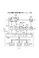
図1は本発明が適用される光送信機の基本構成を示すブロック図である。光源2はあらかじめ定められた波長を有するキャリア光を出力する。光源2としてはレーザダイオードを用いることができ、この場合キャリア光のパワーはレーザダイオードに供給されるバイアス電流により調整可能である。
【0018】
EA変調器4は、光源2からのキャリア光を受けて、強度変調された信号光を出力する。EA変調器4は、印加電圧に応じてキャリア光を吸収することにより信号光を生成する。
【0019】
バイアス回路6はバイアス電圧を発生する。バイアス電圧は、EA変調器4が与えられたチャープパラメータを有するように適切に決定される。与えられたチャープパラメータに対応するバイアス電圧の決定については後述する。
【0020】
駆動回路8は、供給された入力信号に対応する変調信号を発生してこれをバイアス電圧に重畳する。変調信号及びバイアス電圧は印加電圧として光変調器4に供給される。
【0021】
制御手段10は、前述の与えられたチャープパラメータにより決定されるバイアス電圧に応じて最適値が変化し得るパラメータをバイアス電圧に基づいて調整する。このパラメータは、例えば、変調信号の振幅及びデューティ並びにキャリア光のパワーを含むパラメータ群から選択される。
【0022】
EA変調器4が印加電圧の絶対値が大きくなるに従って出力光パワーが小さくなるような特性カーブを有している場合には、バイアス電圧の絶対値が大きくなるに従ってキャリア光のパワーが大きくなるように該パワーが制御される。これにより、EA変調器4の出力光パワーの変動を小さくし乃至は出力光パワーを一定に保つことができる。
【0023】
また、EA変調器4が例えば前述のような特定の特性カーブを有している場合には、バイアス電圧の絶対値が大きくなるに従って変調信号の振幅が大きくなるように該振幅が制御される。これにより、信号光の消光比の変動を小さくし乃至は消光比を一定に保つことができる。
【0024】
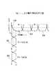
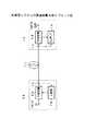
図2は本発明に適用可能な変調器集積化レーザダイオード(MI−LD)の構成を示す図である。MI−LDは、例えばGaInAsの多重量子井戸(MQW)層を含む直接結合導波路構造を有する半導体チップとして提供される。
【0025】
図示の例では、MI−LD12は、キャリア光を発生する発光層(活性層)を有する分布帰還(DFB)タイプのレーザダイオード(LD)16と、吸収層18を有するEA変調器20とを一体に有している。活性層14及び吸収層18はモノリシックに直結されている。
【0026】
符号22はLD16及びEA変調器20に共通な電極を表しており、この電極22は例えば接地される。LD16はバイアス電流を受けるための電極24を有しており、EA変調器20は印加電圧のための電極26を有している。
【0027】
このMI−LD12は、モノリシックに直結される活性層14及び吸収層18を有しているので、活性層14で発生したキャリア光は効率よく吸収層18に導入される。従って、高出力な光送信機の提供が可能になる。また、図1の光源2及びEA変調器4を一つの微細な半導体チップとして提供することができるので、光送信機を小型にすることができる。
【0028】
図3は図2のMI−LDの静特性の一例を示す図である。縦軸はEA変調器20から出力される光のパワー(mW)、横軸はLD16のバイアス電流を示している。電極22を接地して、電極26の電位をそれぞれ0V,−1V,−2V及び−3Vに設定したときの静特性が示されている。
【0029】
この特性から、例えば、ハイレベルが0Vでローレベルが−3Vのパルス波形によりEA変調器12を駆動することによって、消光比が約12dBの光パルス波形が得られることがわかる。
【0030】
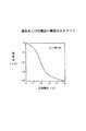
図4は図2のMI−LDにおける減衰率(dB)と印加電圧(V)の関係を示すグラフである。縦軸の減衰率はdB表示であるので、縦軸はMI−LDの出力光パワーの常用対数に対応していることに留意されたい。
【0031】
図2に例示されたMI−LDにおいては、EA変調器20が逆バイアスで駆動されるので、電極26には負の印加電圧が与えられる。図4には、LD16のバイアス電流が100mAであるときの特性が示されており、印加電圧の絶対値が大きくなるに従って減衰が大きくなることが明らかである。
【0032】
図5は図2のMI−LDの動作特性を示す図である。符号28はMI−LDの出力光パワー(mW)と印加電圧(V)との関係を表す特性カーブを示している。縦軸の出力光パワーの目盛がリニアであることから、特性カーブ28の形状は図4のカーブの形状と異なる点に留意されたい。
【0033】
特性カーブ28は、印加電圧の絶対値が大きくなるに従って小さくなる傾斜を有している。
今、変調信号のデューティDが符号30で示されるように100%である場合、特性カーブ28が上述のような形状を有していることに起因して、信号光の出力波形におけるクロスポイントはハイレベル(H)とローレベル(L)の中点より下がる。
【0034】
ここで、変調信号のデューティが100%であるというのは、デジタル信号における立ち上がり線と立ち下がり線のクロスポイントがハイレベル(H)とローレベル(L)の中点に一致することを意味する。また、デューティが100%よりも小さいというのは、クロスポイントがローレベルに近いことを意味し、デューティが100%よりも大きいというのは、クロスポイントがハイレベルに近いことを意味する。
【0035】
信号光波形におけるクロスポイントが中点になるようにシステムが設計されている場合、電気波形から光波形への上述のようなデューティの変化は、受信感度を劣化させる。
【0036】
符号34で示されるように、信号光の出力波形における立ち上がり線と立ち下がり線のクロスポイントがハイレベルとローレベルの中点に一致するようにするためには、符号36で示されるように、変調信号のデューティをあらかじめ100%よりも大きくしておくことが要求されるのである。具体的には、図1の駆動回路8に供給される入力信号(入力データ)のデューティは通常100%に設定されているので、駆動回路8がバイアス電圧に重畳する変調信号のデューティを適切な信号光の出力波形が得られるように調整すべきなのである。
【0037】
図6の(A)及び(B)並びに図7の(A)及び(B)は、デューティの変化の実際の例を示している。10Gb/sのNRZ変調が行われており、各データの横軸の1目盛は20psに対応している。
【0038】
図6の(A)に符号30′で示される波形記録は図5の符号30で示される変調信号に対応しており、デューティは100%である。図6の(B)に符号32′で示される波形記録は図5の符号32で示される信号光の出力波形に対応しており、クロスポイントは下がっている。即ち、クロスポイントはローレベルに近くなっている。
【0039】
図7の(A)に符号36′で示される波形記録は図5の符号36で示される変調信号の波形に対応しており、デューティは100%よりも大きい。図7の(B)に符号34′で示される波形記録は図5の符号34で示される信号光の出力波形に対応しており、クロスポイントは中点にある。
【0040】
信号光の出力波形のクロスポイントが中点になるようにするための変調信号のデューティの目標値は、一般的には、図5の特性カーブ28のどの領域を用いているか、つまり図1のバイアス回路6がどれだけのバイアス電圧を発生しているかによって変化する。そのため、信号光の出力波形におけるクロスポイントがハイレベルとローレベルの中点に対応するように変調信号のデューティを制御することが、受信感度を高める上で望ましいのである。この変調信号のデューティの制御は、例えばバイアス電圧に基づいて行われる。具体的な制御の態様は後述する。
【0041】
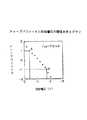
図2のMI−LDのチャープパラメータが測定された。図8はキャリア光のためのバイアス電流を70mAとし、印加電圧(V)の種々の値に対応するチャープパラメータ(無単位)の測定値を示したものである。
【0042】
チャープパラメータは、光変調器における吸収スペクトル、屈折率分散の変化率及び動作波長から決定される量であり、光変調器において生じる波長チャープ量Δλは、このチャープパラメータαを用いて次式で与えられる。
【0043】
【数1】
ここで、λはキャリア光の波長、cは光速、Pは光出力である。このように、光変調器の波長チャープを低減するためには、できる限りチャープパラメータαを零に近づけてやればよいことになる。更に、チャープパラメータαを負にすることにより、ブルーシフトのチャーピングを有する信号光(光パルス)を得ることができる。
【0045】
光変調器から出力される光パルスにブルーシフトのチャーピングを与えておくことにより、異常分散を有する光ファイバによりこの光パルスを伝送したときに、波長分散によるパルス広がりを小さくすることができる。即ちパルス圧縮が可能である。具体的には次の通りである。
【0046】
一般に、単一モードファイバにおいては、零分散波長よりも短波長側では波長が長くなるのに従って群速度が増大し(正常分散領域)、零分散波長よりも長波長側では波長が長くなるのに従って群速度が減少する(異常分散領域)。
【0047】
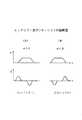
例えば、零分散波長が1.3μm帯にあるシリカファイバにより1.55μm帯の光パルスを伝送する場合には、異常分散によるレッドシフトが生じて波形が拡がるので、光変調器がブルーシフトの信号光を出力するように、チャープパラメータαが設定される。これがプリチャープである。
【0048】
図9の(A)はレッドシフト(α>0)に対応しており、光パルスの立ち上がり及び立ち下がりにそれぞれ短波長側及び長波長側へのシフトが生じている。
図9の(B)はブルーシフト(α<0)に対応しており、光パルスの立ち上がり及び立ち下がりでそれぞれ長波長側及び短波長側へのシフトが生じている。
【0049】
尚、図9の(A)及び図9の(B)において、それぞれ光パルスは時間軸(t)上を左から右に向かって進むものとする。Pはパワー又は電界振幅、λは波長を表している。
【0050】
図10は図2のMI−LDを有する光送信機の実施形態を示すブロック図である。図1の制御手段10は、A/Dコンバータ及びD/Aコンバータを含む信号入出力用のI/Oポート38と、あらかじめ定められたプログラムに従ってバイアス電流の目標値等の演算を行うCPU(中央演算ユニット)40と、プログラム及びデータテーブルのためのデータが記憶されているROM(リードオンリーメモリ)42と、演算結果を一時的に記憶するためのRAM(ランダムアクセスメモリ)44と、これらを相互に接続するデータバス46とを備えている。
【0051】
MI−LD12には温度コントローラ48が付随的に設けられている。MI−LD12の温度データは、温度コントローラ48からI/Oポート38を介してCPU40に取り込まれる。温度の目標値は、CPU40からI/Oポート38を介して温度コントローラ48に供給される。
【0052】
バイアス電流回路50は、キャリア光を出力するLD16にバイアス電流ILDを供給する。バイアス電流の目標値は、CPU40からI/Oポート38を介してバイアス電流回路50に供給される。
【0053】
EA変調器20のためにバイアス電圧回路6が発生するバイアス電圧VBの値は、I/Oポート38を介してCPU40に取り込まれる。これは、バイアス電圧に基づいて変調信号VMODの振幅等を制御するためである。
【0054】
EA変調器20が与えられたチャープパラメータを有するように設定されるバイアス電圧の目標値は、CPU40からI/Oポート38を介してバイアス電圧回路6に供給される。
【0055】
変調信号VMODをバイアス電圧VBに重畳する駆動回路8には、振幅可変回路54が付随的に設けられている。振幅可変回路54には、振幅の目標値がCPU40からI/Oポート38を介して供給されており、振幅可変回路54は駆動回路8が出力する変調信号の振幅が目標値に一致するようにこれを制御する。
【0056】
デューティ可変回路56は、駆動回路8が出力する変調信号VMODのデューティを制御する。デューティの目標値は、CPU40からI/Oポート38を介してデューティ可変回路56に供給される。
【0057】
MI−LD12から出力された信号光は、ビームスプリッタ58によりトータル出力の大部分に相当する第1の分岐光と残りの第2の分岐光とに分岐される。第1の分岐光は図示しない光伝送路に送出され、第2の分岐光はフォトディテクタ60に供給される。フォトディテクタ60は供給された一部の信号光を電気信号に変換し、この電気信号はI/Oポート38を介してCPU40に取り込まれる。
【0058】
この光送信機は、チャープパラメータの設定データや後述する受信側における伝送特性のモニタリングデータ等を入力するためのポート62を有している。入力データはI/Oポート38を介してCPU40に取り込まれる。
【0059】
図11の(A)及び(B)は図10の光送信機の動作を説明するための図である。
図11の(A)は、負のチャープパラメータの領域で動作させるために比較的絶対値が大きいバイアス電圧VB−が設定されている場合に対応している。図示された例では、バイアス電圧VB−は信号光の出力波形におけるクロスポイントに対応しているが、信号光波形におけるハイレベルに対応するチャープパラメータが概ね支配的であることから、バイアス電圧の目標値を信号光波形のハイレベルに対応させてもよい。
【0060】
図11の(A)及び(B)に示される特性カーブは図5の特性カーブに対応しているものとする。
出力信号光の消光比を改善するためには、バイアス電圧の絶対値が大きくなるに従って変調信号の振幅が大きくなるようにすることが望ましい。図11の(A)では、変調信号の振幅V1に対して出力信号光の消光比は1:3になっている。
【0061】
また、信号光の出力波形におけるクロスポイントがハイレベルとローレベルの中点になるように、変調信号のデューティはD1(>100%)に設定されている。
【0062】
変調信号の振幅及びデューティの最適値は、特性カーブが与えられるとバイアス電圧に対して一義的に決定されるので、バイアス電圧の各値に対応する最適な変調信号の振幅及びデューティの値が図10のROM42に記憶されており、CPU40はこの記憶テーブルに基づき変調信号の振幅及びデューティの目標値を算出するのである。
【0063】
図11の(B)に示されるように、正のチャープパラメータの領域で動作させるために比較的絶対値が小さいバイアス電圧VB+が設定されると、消光比が一定に保たれるようにするために、変調信号の振幅がV2(<V1)に変更される。また、信号光の出力波形におけるクロスポイントがハイレベルとローレベルの中間になるように、変調信号のデューティがD2(>D1)に変更される。
【0064】
ここで注意すべき点は、キャリア光のパワーが一定である場合、EA変調器のバイアス電圧の絶対値が大きくなるのに従って信号光の出力パワーが減少している点である。そこで、この実施形態では、バイアス電圧の絶対値が大きくなるに従ってキャリア光のパワーが大きくなるように、バイアス電流回路50がLD16に供給するバイアス電流の目標値が設定される。
【0065】
EA変調器のバイアス電圧の変更に伴う信号光の出力パワーの変動を抑えるために、フィードフォワード制御が採用可能である。特性カーブが与えられると、バイアス電圧の各値に対するLDバイアス電流の最適値がわかるので、これをROM42に記憶させておき、バイアス電圧回路6から取り込まれるバイアス電圧の値に基づいてCPU40がLDバイアス電流の最適値を算出する。
【0066】
図10の実施形態では、出力信号光の一部を受けるフォトディテクタ60が設けられているので、LDバイアス電流のフィードバック制御も可能である。即ち、フォトディテクタ60の出力信号レベルが一定になるように、CPU40が逐次LDバイアス電流の目標値を算出し、そのバイアス電流をバイアス電流回路50がLD16に供給するのである。
【0067】
さて、ブルーシフトのプリチャーピングを得るというメリットのために、EA変調器に供給されるバイアス電圧の絶対値を大きくすると、出力信号光の消光比が劣化し且つ光出力パワーが低下するというデメリットが生じる。従って、このようなトレードオフの関係を考慮して、光伝送路における損失や波長分散に合わせてEA変調器の駆動条件を決定するのが望ましい。制御対象となる駆動パラメータとしては、前述のEA変調器のバイアス電圧、変調信号のデューティ及び振幅並びにLDバイアス電流の他に、EA変調器単独の温度又はMI−LDの温度がある。
【0068】
本発明は、与えられたチャープパラメータに対応して決定されるEA変調器のバイアス電圧に基づいて1つの駆動パラメータが制御されることのみによって限定されるが、複数の駆動パラメータを連動させて制御することが望ましい。
【0069】
例えば、EA変調器のバイアス電圧の絶対値が大きくなると消光比が劣化するので、これを補償するために変調信号の振幅が大きくされるが、振幅の拡大には限度がある。このような場合に消光比を改善するために、駆動パラメータ群から光変調器の温度が選択されるのである。具体的には次の通りである。
【0070】
図10の光送信機において、MI−LD12の温度を増加させると、LD16とEA変調器20との間の波長デチューニング量、即ちLD16から出力されるキャリア光の波長とEA変調器20におけるバンドギャップを与える波長との差が減少することにより、消光比が改善される。この減少は出力光パワーと印加電圧を関係付ける特性カーブの形状が変化することにより理解することができる。
【0071】
従って、温度が制御対象となる場合には、特性カーブの変化により他の制御対象となる駆動パラメータの最適値が異なるものとなるので、ROM42は温度の各値毎にあらかじめ設定されたデータテーブルを有していることが望ましい。
【0072】
このように本発明のある実施形態においては、図1の制御手段10は、EA変調器4のバイアス電圧が大きくなるに従ってEA変調器の温度が上昇するように該温度を制御する手段を含む。
【0073】
また、この種のデータテーブルを作成する場合には、LD16の温度が上昇するとキャリア光のパワーが減少することを考慮すべきである。
図10の光送信機においては、光源2及びEA変調器4(図1参照)としてM1−LD12を用いているので、光源及び変調器間の結合効率を高めることができ、高出力で且つ小型な光送信機の提供が可能である。また、光源及び変調器の温度制御を1つの温度コントローラ48により行うことができる。
【0074】
本発明の他の実施形態においては、図10のバイアス電圧回路6は、正の第1のチャープパラメータを与える第1のバイアス電圧と負の第2のチャープパラメータを与える第2のバイアス電圧とを選択的に発生する手段を含む。
【0075】
例えば図8において、点A及びBによりそれぞれ示される+1及び−1のチャープパラメータを切り換えるために、第1及び第2のバイアス電圧としてそれぞれ−0.4V及び−1.7Vが与えられる。
【0076】
この場合、制御手段10は、1つ又は複数の駆動パラメータを第1及び第2のバイアス電圧にそれぞれ対応する2つの値の間で切り換える手段を含んでいれば足りるので、CPU40における演算が簡単になる。
【0077】
このように正負で絶対値の等しいチャープパラメータの切り換えは、MZ変調器による場合と同様に有用な光送信機の提供を可能にする。MZ変調器においては、正弦波に近似される動作特性カーブ上で動作点を半周期変えるだけで、簡単にチャープパラメータの正負の切り換えが可能である。
【0078】
図12は本発明の光通信システムの実施形態を示すブロック図である。このシステムは、光送信機64を有する第1の端局66と、光受信機68を有する第2の端局70と、端局66及び70を結ぶ光ファイバ伝送路72とを備えている。
【0079】
光送信機64は図1の基本構成望ましくは図10の実施形態を有している。光送信機64は、入力信号に基づいて信号光を生成し、これを光ファイバ伝送路72の第1端に入力する。
【0080】
光ファイバ伝送路72により伝送されその第2端から出力された信号光は、光受信機68に供給され、光受信機68は光送信機64の入力信号に対応する出力信号を復調する。
【0081】
第2の端局70は、更に、受けた信号光に関する伝送特性をモニタリングするモニタリング回路73と、そのモニタリングデータを光ファイバ伝送路72に逆方向に結合する手段74とを有している。
【0082】
このモニタリングデータは第1の端局66へ伝送される。第1の端局66は、伝送されたモニタリングデータを取り出す手段76と、このデータに基づいて光送信機64におけるチャープパラメータを設定するチャープパラメータ設定回路78とを有している。
【0083】
モニタリング回路73において測定される伝送特性としては、符号誤り率(BER)、電気信号の信号対雑音比(Q値)、信号中のバリティビットのチェック、等符号誤り率曲線、アイマスクパターン等が挙げられる。
【0084】
光ファイバ伝送路72が1.3μm帯に零分散波長を有するシリカファイバからなる場合には、前述したように、1.55μm帯の信号光に対してチャープパラメータ設定回路78は負のチャープパラメータを設定する。即ち、チャープパラメータは光ファイバ伝送路72の波長分散に応じて与えられる。
【0085】
図12のシステムにおいては、光送信機64が本発明の駆動装置を含んでいるので、光ファイバ伝送路72における損失や波長分散の違い(経時変化も含む)に応じて最適な伝送特性を得ることができる。即ち、システムの設計や変更に際して柔軟に対応可能な汎用性の高い光変調器若しくはその駆動回路又は光送信機の提供が可能になる。
【0086】
尚、運用回線(光ファイバ伝送路72)と敷設環境のほぼ等しい図示しない予備回線が存在する場合には、サービスダウンを避けるため、まず予備回線において各駆動パラメータの最適化を行った後、それらを参照して運用回線に適用することもできる。モニタリングデータの伝送は、電気回線又は無線回線により行ってもよい。
【0087】
【発明の効果】
以上説明したように、本発明によると、適用されるシステムに適合するようにチャープパラメータを任意に設定可能な光変調器の駆動方法及び装置の提供が可能になるという効果が生じる。
【0088】
また、本発明の方法又は装置が適用される光通信システムの提供が可能になるという効果が生じる。
【図面の簡単な説明】
【図1】本発明が適用される光送信機の基本構成を示すブロック図である。
【図2】MI−LD(変調器集積化レーザダイオード)の構成を示す図である。
【図3】出力光パワーとLDバイアス電流の関係を示すグラフである。
【図4】EA変調器の減衰率と印加電圧の関係を示すグラフである。
【図5】MI−LDの動作特性を示す図である。
【図6】変調信号波形のクロスポイントが中点にある場合を示す図である。
【図7】信号光波形のクロスポイントが中点にある場合を示す図である。
【図8】チャープパラメータと印加電圧の関係を示すグラフである。
【図9】レッドシフト及びブルーシフトの説明図である。
【図10】本発明が適用される光送信機の実施形態を示すブロック図である。
【図11】図10の光送信機の動作説明図である。
【図12】本発明の光通信システムの実施形態を示すブロック図である。
【符号の説明】
2 光源
4 EA変調器
6 バイアス(電圧)回路
8 駆動回路
10 制御手段[0001]
BACKGROUND OF THE INVENTION
The present invention relates generally to driving an electroabsorption optical modulator, and more particularly to a driving method and apparatus for an electroabsorption optical modulator and an optical communication system to which the apparatus is applied.
[0002]
In recent years, with the rapid increase in the amount of information, it is desired to increase the capacity of optical communication systems. For this reason, the transmission rate, that is, the modulation rate is increased. In direct intensity modulation of a laser diode, relatively large chirping (dynamic wavelength fluctuation due to relaxation oscillation or the like) limits the transmission distance and modulation speed.
[0003]
When signal light having chirping passes through an optical fiber having chromatic dispersion (chromatic dispersion), waveform distortion usually occurs. In order to avoid this problem, there is an increasing expectation for the use of an external optical modulator that is generally less likely to cause chirping.
[0004]
[Prior art]
A Mach-Zehnder type optical modulator (MZ modulator) has been developed as a practical external optical modulator. Carrier light of constant intensity from the light source is supplied to the MZ modulator, and intensity-modulated signal light is obtained by a switching operation using light interference. For example, LiNbO3MZ modulator using crystal (Seino et al., IEICE Technical Report LQE89-35) and MZ modulator using compound semiconductor crystal (Inoue, Proceedings of 8th Optical Symposium pp. 25-29) Has been reported.
[0005]
The drawbacks of MZ modulators that are often pointed out are that a relatively large drive voltage is required, and that automatic bias control (Automatic Bias Control) is required to keep the operating point constant, and the apparatus tends to be large-scale. There are.
[0006]
In view of these drawbacks, an electroabsorption optical modulator (EA modulator) has been proposed as an external optical modulator that can be driven at low power and is suitable for miniaturization. The EA modulator generates intensity-modulated signal light by absorbing carrier light according to the applied voltage. For example, an EA modulator using a compound semiconductor crystal (Yamada et al., IEICE Technical Report LQE95-17) has been reported.
[0007]
A practical EA modulator is provided as a semiconductor chip by a semiconductor lamination technique. This EA modulator can be easily integrated with a laser diode as a carrier light source, thereby enabling high output by reducing coupling loss between the light source and the modulator, and miniaturization by integration. For example, a semiconductor chip in which a DFB-LD (distributed feedback laser diode) and an EA modulator are monolithically integrated (Morito et al., IEICE Technical Report LQE95-17, pp. 1-6) has been reported. .
[0008]
[Problems to be solved by the invention]
By the way, it became clear that wavelength chirp generate | occur | produces with the phase modulation component induced depending on the optical modulator (F. Koyama, and K. Iga: J. Lightwave Technol., LT-6, (1988) pp. .87-93). The amount of wavelength chirp produced is uniformly represented by the chirp parameter of the optical modulator.
[0009]
Depending on whether the chirp parameter is positive or negative, the transmitted optical pulse is spread or compressed. When signal light in the 1.55 μm band is transmitted by a silica fiber having a zero dispersion wavelength in the 1.3 μm band, a positive chirp parameter gives pulse broadening, and a negative chirp parameter gives pulse compression.
[0010]
It has been reported that generating appropriate chirping (pre-chirp) in the transmission waveform in advance increases the transmission distance dramatically (K. Morito, R. Sahara, K. Sato, Y. Kotani, and H. Soda “MQW Modulator Integrated DFB Lasers for Multigigabit Transmisson Systems” Proc. 21st Eur. Conf. on Opt. Comm. (ECOC '95 -Brs. 89). Thus, by making it possible to arbitrarily set the chirp parameter of the optical modulator, the performance of the system to which the optical modulator is applied is dramatically improved.
[0011]
Accordingly, an object of the present invention is to provide an optical modulator driving method and apparatus capable of arbitrarily setting a chirp parameter so as to be adapted to an applied system. Another object of the present invention is to provide an optical communication system to which the driving method or apparatus is applied.
[0012]
[Means for Solving the Problems]
According to one aspect of the present invention, a driving apparatus for an EA modulator is provided. The EA modulator receives the carrier light from the light source, and absorbs the carrier light according to the applied voltage, thereby outputting the intensity-modulated signal light.The EA modulator has a characteristic curve in which the output optical power decreases as the absolute value of the applied voltage increases.
[0013]
The bias circuit generates a bias voltage that is determined so that the optical modulator has a given chirp parameter.
The drive circuit receives the input signal, generates a modulation signal corresponding to the input signal, superimposes the modulation signal on the bias voltage, and supplies it to the optical modulator as an applied voltage.
[0014]
The control meansThe amplitude of the modulation signal increases as the absolute value of the bias voltage increases.Modulation signal amplitudeAnd controllingAt least one parameter selected from the parameter group including the duty and the power of the carrier light is adjusted based on the bias voltage.
[0015]
According to another aspect of the present invention, a driving method according to the operation of the driving device is provided.
According to still another aspect of the present invention, a first terminal station having an optical transmitter, a second terminal station having an optical receiver, and an optical fiber transmission line connecting the first and second terminal stations are provided. An optical communication system is provided.
[0016]
An optical transmitter includes a light source that outputs carrier light, an EA modulator that receives carrier light and absorbs carrier light according to an applied voltage, and outputs signal light that has been intensity-modulated, and the driving device according to the present invention described above. And.
[0017]
DETAILED DESCRIPTION OF THE INVENTION
Hereinafter, preferred embodiments of the present invention will be described in detail with reference to the accompanying drawings.
FIG. 1 is a block diagram showing a basic configuration of an optical transmitter to which the present invention is applied. The
[0018]
The
[0019]
The
[0020]
The
[0021]
The control means 10 adjusts a parameter whose optimum value can be changed according to the bias voltage determined by the given chirp parameter based on the bias voltage. This parameter is selected from a parameter group including, for example, the amplitude and duty of the modulation signal and the power of the carrier light.
[0022]
When the
[0023]
When the
[0024]
FIG. 2 is a diagram showing a configuration of a modulator integrated laser diode (MI-LD) applicable to the present invention. The MI-LD is provided as a semiconductor chip having a direct coupling waveguide structure including, for example, a GaInAs multiple quantum well (MQW) layer.
[0025]
In the example shown in the figure, the MI-LD 12 is an integrated body of a distributed feedback (DFB) type laser diode (LD) 16 having a light emitting layer (active layer) that generates carrier light and an
[0026]
[0027]
Since the MI-LD 12 has the
[0028]
FIG. 3 is a diagram showing an example of the static characteristics of the MI-LD of FIG. The vertical axis represents the power (mW) of light output from the
[0029]
From this characteristic, it can be seen that, for example, by driving the EA modulator 12 with a pulse waveform having a high level of 0V and a low level of -3V, an optical pulse waveform having an extinction ratio of about 12 dB can be obtained.
[0030]
FIG. 4 is a graph showing the relationship between the attenuation rate (dB) and the applied voltage (V) in the MI-LD of FIG. Note that since the vertical axis attenuation is expressed in dB, the vertical axis corresponds to the common logarithm of the output optical power of the MI-LD.
[0031]
In the MI-LD illustrated in FIG. 2, since the
[0032]
FIG. 5 is a diagram showing operating characteristics of the MI-LD of FIG.
[0033]
The
Now, when the duty D of the modulation signal is 100% as indicated by
[0034]
Here, the duty of the modulation signal being 100% means that the cross point of the rising line and the falling line in the digital signal coincides with the midpoint of the high level (H) and the low level (L). . A duty smaller than 100% means that the cross point is close to a low level, and a duty larger than 100% means that the cross point is close to a high level.
[0035]
When the system is designed so that the cross point in the signal light waveform is the middle point, the above-described change in duty from the electric waveform to the optical waveform degrades the reception sensitivity.
[0036]
As indicated by
[0037]
6A and 6B and FIG. 7A and FIG. 7B show actual examples of changes in duty. 10 Gb / s NRZ modulation is performed, and one scale on the horizontal axis of each data corresponds to 20 ps.
[0038]
The waveform record indicated by reference numeral 30 'in FIG. 6A corresponds to the modulation signal indicated by
[0039]
The waveform recording indicated by reference numeral 36 'in FIG. 7A corresponds to the waveform of the modulation signal indicated by
[0040]
In general, the target value of the duty of the modulation signal for making the cross point of the output waveform of the signal light the middle point is the region of the
[0041]
The chirp parameters of the MI-LD in FIG. 2 were measured. FIG. 8 shows measured values of chirp parameters (no unit) corresponding to various values of the applied voltage (V) when the bias current for the carrier light is 70 mA.
[0042]
The chirp parameter is an amount determined from the absorption spectrum in the optical modulator, the rate of change of refractive index dispersion, and the operating wavelength. The wavelength chirp amount Δλ generated in the optical modulator is given by the following equation using this chirp parameter α. It is done.
[0043]
[Expression 1]
Here, λ is the wavelength of the carrier light, c is the speed of light, and P is the optical output. Thus, in order to reduce the wavelength chirp of the optical modulator, the chirp parameter α should be as close to zero as possible. Further, by making the chirp parameter α negative, it is possible to obtain signal light (light pulse) having blue shift chirping.
[0045]
By applying blue shift chirping to the optical pulse output from the optical modulator, the pulse spread due to chromatic dispersion can be reduced when the optical pulse is transmitted through an optical fiber having anomalous dispersion. That is, pulse compression is possible. Specifically, it is as follows.
[0046]
In general, in a single mode fiber, the group velocity increases as the wavelength becomes longer on the shorter wavelength side than the zero dispersion wavelength (normal dispersion region), and the wavelength becomes longer on the longer wavelength side than the zero dispersion wavelength. The group velocity decreases (anomalous dispersion region).
[0047]
For example, when a 1.55 μm band optical pulse is transmitted through a silica fiber having a zero dispersion wavelength in the 1.3 μm band, a red shift due to anomalous dispersion occurs and the waveform expands. The chirp parameter α is set so as to output light. This is pre-chirp.
[0048]
FIG. 9A corresponds to a red shift (α> 0), and shifts to the short wavelength side and the long wavelength side occur at the rise and fall of the optical pulse, respectively.
FIG. 9B corresponds to the blue shift (α <0), and shifts to the long wavelength side and the short wavelength side occur at the rise and fall of the optical pulse, respectively.
[0049]
In FIG. 9A and FIG. 9B, it is assumed that each light pulse travels from left to right on the time axis (t). P represents power or electric field amplitude, and λ represents wavelength.
[0050]
FIG. 10 is a block diagram showing an embodiment of an optical transmitter having the MI-LD of FIG. 1 includes an A / D converter and a signal input / output I / O port 38 including a D / A converter, and a CPU (central control unit) that calculates a target value of a bias current according to a predetermined program. (Arithmetic unit) 40, ROM (read-only memory) 42 in which data for programs and data tables are stored, RAM (random access memory) 44 for temporarily storing calculation results, And a data bus 46 connected to the.
[0051]
The MI-LD 12 is provided with a temperature controller 48. The temperature data of the MI-LD 12 is taken into the
[0052]
The bias
[0053]
Bias voltage V generated by the
[0054]
The target value of the bias voltage set so that the
[0055]
Modulation signal VMODThe bias voltage VBAn amplitude variable circuit 54 is incidentally provided in the
[0056]
The duty variable circuit 56 is a modulation signal V output from the drive circuit 8.MODTo control the duty. The target value of the duty is supplied from the
[0057]
The signal light output from the MI-LD 12 is branched by the beam splitter 58 into a first branched light corresponding to most of the total output and the remaining second branched light. The first branched light is sent to an optical transmission path (not shown), and the second branched light is supplied to the photodetector 60. The photodetector 60 converts a part of the supplied signal light into an electrical signal, and this electrical signal is taken into the
[0058]
This optical transmitter has a port 62 for inputting chirp parameter setting data, transmission characteristics monitoring data on the receiving side, which will be described later, and the like. Input data is taken into the
[0059]
11A and 11B are diagrams for explaining the operation of the optical transmitter of FIG.
FIG. 11A shows a bias voltage V having a relatively large absolute value in order to operate in the negative chirp parameter region.B-It corresponds to when is set. In the illustrated example, the bias voltage VB-Corresponds to the cross point in the output waveform of the signal light, but the chirp parameter corresponding to the high level in the signal light waveform is almost dominant, so the target value of the bias voltage corresponds to the high level of the signal light waveform You may let them.
[0060]
The characteristic curves shown in FIGS. 11A and 11B correspond to the characteristic curves in FIG.
In order to improve the extinction ratio of the output signal light, it is desirable to increase the amplitude of the modulation signal as the absolute value of the bias voltage increases. In FIG. 11A, the extinction ratio of the output signal light is 1: 3 with respect to the amplitude V1 of the modulation signal.
[0061]
In addition, the duty of the modulation signal is set to D1 (> 100%) so that the cross point in the output waveform of the signal light is a midpoint between the high level and the low level.
[0062]
Since the optimum values of the amplitude and duty of the modulation signal are uniquely determined for the bias voltage when the characteristic curve is given, the optimum amplitude and duty of the modulation signal corresponding to each value of the bias voltage are shown in FIG. The
[0063]
As shown in FIG. 11B, the bias voltage V having a relatively small absolute value in order to operate in the positive chirp parameter region.B +Is set, the amplitude of the modulation signal is changed to V2 (<V1) in order to keep the extinction ratio constant. Further, the duty of the modulation signal is changed to D2 (> D1) so that the cross point in the output waveform of the signal light is intermediate between the high level and the low level.
[0064]
What should be noted here is that when the power of the carrier light is constant, the output power of the signal light decreases as the absolute value of the bias voltage of the EA modulator increases. Therefore, in this embodiment, the target value of the bias current that the bias
[0065]
Feed forward control can be employed to suppress fluctuations in the output power of the signal light accompanying changes in the bias voltage of the EA modulator. When the characteristic curve is given, the optimum value of the LD bias current for each value of the bias voltage can be known, and this value is stored in the ROM 42, and the
[0066]
In the embodiment of FIG. 10, since the photodetector 60 that receives a part of the output signal light is provided, feedback control of the LD bias current is also possible. That is, the
[0067]
Now, in order to obtain the blue shift pre-chirping, if the absolute value of the bias voltage supplied to the EA modulator is increased, the extinction ratio of the output signal light deteriorates and the optical output power decreases. Occurs. Therefore, in consideration of such a trade-off relationship, it is desirable to determine the driving condition of the EA modulator in accordance with the loss and chromatic dispersion in the optical transmission line. The drive parameters to be controlled include the temperature of the EA modulator alone or the temperature of the MI-LD in addition to the bias voltage of the EA modulator, the duty and amplitude of the modulation signal, and the LD bias current.
[0068]
The present invention is limited only by the control of one drive parameter based on the bias voltage of the EA modulator determined corresponding to a given chirp parameter. However, the present invention is controlled by interlocking a plurality of drive parameters. It is desirable to do.
[0069]
For example, when the absolute value of the bias voltage of the EA modulator increases, the extinction ratio deteriorates. Therefore, the amplitude of the modulation signal is increased to compensate for this, but there is a limit to the increase of the amplitude. In such a case, the temperature of the optical modulator is selected from the drive parameter group in order to improve the extinction ratio. Specifically, it is as follows.
[0070]
In the optical transmitter of FIG. 10, when the temperature of the MI-LD 12 is increased, the wavelength detuning amount between the
[0071]
Therefore, when the temperature is to be controlled, the optimum value of the drive parameter to be controlled differs depending on the change of the characteristic curve. Therefore, the ROM 42 stores a data table set in advance for each temperature value. It is desirable to have.
[0072]
Thus, in one embodiment of the present invention, the control means 10 of FIG. 1 includes means for controlling the temperature so that the temperature of the EA modulator increases as the bias voltage of the
[0073]
Further, when creating this type of data table, it should be considered that the power of the carrier light decreases as the temperature of the
In the optical transmitter of FIG. 10, since the M1-LD 12 is used as the
[0074]
In another embodiment of the present invention, the
[0075]
For example, in FIG. 8, to switch the +1 and -1 chirp parameters indicated by points A and B, respectively, -0.4V and -1.7V are applied as the first and second bias voltages, respectively.
[0076]
In this case, the control means 10 only needs to include means for switching one or a plurality of drive parameters between two values corresponding to the first and second bias voltages, respectively. Become.
[0077]
The switching of the chirp parameters having the same positive and negative values and absolute values in this manner makes it possible to provide a useful optical transmitter as in the case of the MZ modulator. In the MZ modulator, the chirp parameter can be switched between positive and negative simply by changing the operating point on the operating characteristic curve approximated to a sine wave by a half cycle.
[0078]
FIG. 12 is a block diagram showing an embodiment of the optical communication system of the present invention. This system includes a first terminal station 66 having an optical transmitter 64, a
[0079]
The optical transmitter 64 has the basic configuration of FIG. 1, preferably the embodiment of FIG. The optical transmitter 64 generates signal light based on the input signal, and inputs this to the first end of the optical fiber transmission line 72.
[0080]
The signal light transmitted through the optical fiber transmission path 72 and output from the second end thereof is supplied to the optical receiver 68, and the optical receiver 68 demodulates the output signal corresponding to the input signal of the optical transmitter 64.
[0081]
The
[0082]
This monitoring data is transmitted to the first terminal station 66. The first terminal station 66 has means 76 for extracting transmitted monitoring data, and a chirp parameter setting circuit 78 for setting a chirp parameter in the optical transmitter 64 based on this data.
[0083]
Transmission characteristics measured in the monitoring circuit 73 include a code error rate (BER), a signal-to-noise ratio (Q value) of an electric signal, a check of a parity bit in the signal, an equal code error rate curve, an eye mask pattern, and the like. Is mentioned.
[0084]
When the optical fiber transmission line 72 is made of a silica fiber having a zero dispersion wavelength in the 1.3 μm band, the chirp parameter setting circuit 78 sets a negative chirp parameter for the signal light in the 1.55 μm band as described above. Set. That is, the chirp parameter is given according to the chromatic dispersion of the optical fiber transmission line 72.
[0085]
In the system of FIG. 12, since the optical transmitter 64 includes the drive device of the present invention, optimum transmission characteristics are obtained according to the loss in the optical fiber transmission line 72 and the difference in chromatic dispersion (including changes over time). be able to. In other words, it is possible to provide a highly versatile optical modulator that can flexibly cope with the design or change of the system, a drive circuit thereof, or an optical transmitter.
[0086]
If there is a standby line (not shown) that is almost the same in construction environment as the operation line (optical fiber transmission line 72), the drive parameters are first optimized in the standby line to avoid service down. It can also be applied to operational lines with reference to. The monitoring data may be transmitted through an electric line or a wireless line.
[0087]
【The invention's effect】
As described above, according to the present invention, it is possible to provide an optical modulator driving method and apparatus capable of arbitrarily setting a chirp parameter so as to be adapted to an applied system.
[0088]
In addition, there is an effect that it is possible to provide an optical communication system to which the method or apparatus of the present invention is applied.
[Brief description of the drawings]
FIG. 1 is a block diagram showing a basic configuration of an optical transmitter to which the present invention is applied.
FIG. 2 is a diagram showing a configuration of an MI-LD (modulator integrated laser diode).
FIG. 3 is a graph showing the relationship between output light power and LD bias current.
FIG. 4 is a graph showing the relationship between the attenuation factor of the EA modulator and the applied voltage.
FIG. 5 is a diagram showing operating characteristics of MI-LD.
FIG. 6 is a diagram illustrating a case where a cross point of a modulation signal waveform is at a middle point.
FIG. 7 is a diagram illustrating a case where a cross point of a signal light waveform is at a middle point.
FIG. 8 is a graph showing a relationship between a chirp parameter and an applied voltage.
FIG. 9 is an explanatory diagram of a red shift and a blue shift.
FIG. 10 is a block diagram showing an embodiment of an optical transmitter to which the present invention is applied.
11 is an operation explanatory diagram of the optical transmitter of FIG. 10;
FIG. 12 is a block diagram showing an embodiment of an optical communication system of the present invention.
[Explanation of symbols]
2 Light source
4 EA modulator
6 Bias (voltage) circuit
8 Drive circuit
10 Control means
Claims (14)
Translated fromJapanese与えられたチャープパラメータを上記光変調器が有するように決定されるバイアス電圧を発生するバイアス回路と、
入力信号を受け該入力信号に対応する変調信号を発生してこれを上記バイアス電圧に重畳して上記印加電圧として上記光変調器に供給する駆動回路と、
上記変調信号の振幅及びデューティ並びに上記キャリア光のパワーを含むパラメータ群から選択される少なくとも1つのパラメータを上記バイアス電圧に基づいて調整する制御手段とを備え、
上記光変調器は上記印加電圧の絶対値が大きくなるに従って上記光変調器の出力光パワーが小さくなる特性カーブを有し、上記制御手段は上記バイアス電圧の絶対値が大きくなるに従って上記変調信号の振幅が大きくなるように該振幅を制御する手段を含む装置。A driving device for an electroabsorption optical modulator that receives carrier light from a light source and outputs the intensity-modulated signal light by absorbing the carrier light according to an applied voltage,
A bias circuit for generating a bias voltage determined so that the optical modulator has a given chirp parameter;
A drive circuit that receives an input signal, generates a modulation signal corresponding to the input signal, superimposes the modulation signal on the bias voltage, and supplies the modulation signal to the optical modulator as the applied voltage;
Control means for adjusting at least one parameter selected from a parameter group including the amplitude and duty of the modulation signal and the power of the carrier light based on the bias voltage;
The optical modulator has a characteristic curve in which the output optical power of the optical modulator decreases as the absolute value of the applied voltage increases, and the control means outputs the modulation signal as the absolute value of the bias voltage increases. An apparatuscomprising means for controlling the amplitude so that the amplitude is increased .
上記制御手段は、上記信号光の波形におけるクロスポイントがハイレベルとローレベルの中間に位置するように上記変調信号のデューティを制御する手段を含む請求項1に記載の装置。The characteristic curve has a slope that decreases as the absolute value of the applied voltage increases,
2. The apparatus according to claim1 , wherein the control means includes means for controlling the duty of the modulation signal so that a cross point in the waveform of the signal light is located between the high level and the low level.
上記制御手段は、上記バイアス電圧が変化するのに従って上記光変調器の温度を変化させる手段を含む請求項1に記載の装置。The parameter group further includes a temperature of the light modulator,
2. The apparatus of claim 1, wherein the control means includes means for changing the temperature of the optical modulator as the bias voltage changes.
上記制御手段は、上記パラメータ群から選択される少なくとも1つのパラメータを上記第1及び第2のバイアス電圧にそれぞれ対応する2つの値の間で切り換える手段を含む請求項1に記載の装置。The bias circuit includes means for selectively generating a first bias voltage that provides a first chirp parameter and a second bias voltage that provides a second chirp parameter;
2. The apparatus according to claim 1, wherein the control means includes means for switching at least one parameter selected from the parameter group between two values respectively corresponding to the first and second bias voltages.
上記光変調器は上記キャリア光を吸収する吸収層を有し、
該レーザダイオード及び該光変調器は、上記活性層及び上記吸収層が直結するようにモノリシックに一体であり、
上記キャリア光のパワーは上記バイアス電流により調整される請求項1に記載の装置。The light source comprises a laser diode having an active layer that generates the carrier light having a power corresponding to a supplied bias current,
The optical modulator has an absorption layer that absorbs the carrier light,
The laser diode and the optical modulator are monolithically integrated so that the active layer and the absorption layer are directly connected,
The apparatus according to claim 1, wherein the power of the carrier light is adjusted by the bias current.
上記制御手段は該検出された出力光パワーが一定になるように上記キャリア光のパワーを制御する手段を含む請求項1に記載の装置。Means for detecting the output optical power of the optical modulator;
2. The apparatus according to claim 1, wherein the control means includes means for controlling the power of the carrier light so that the detected output light power becomes constant.
光受信機を有する第2の端局と、
該第1及び第2の端局を結ぶ光ファイバ伝送路とを備え、
上記光送信機は、
キャリア光を出力する光源と、
該キャリア光を受け印加電圧に応じて該キャリア光を吸収することにより強度変調された信号光を出力する電界吸収型光変調器と、
与えられたチャープパラメータを上記光変調器が有するように決定されるバイアス電圧を発生するバイアス回路と、
入力信号を受け該入力信号に対応する変調信号を発生してこれを上記バイアス電圧に重畳して上記印加電圧として上記光変調器に供給する駆動回路と、
上記変調信号の振幅及びデューティ並びに上記キャリア光のパワーを含むパラメータ群から選択される少なくとも1つのパラメータを上記バイアス電圧に基づいて調整する制御手段とを備え、
上記光変調器は上記印加電圧の絶対値が大きくなるに従って上記光変調器の出力光パワーが小さくなる特性カーブを有し、上記制御手段は上記バイアス電圧の絶対値が大きくなるに従って上記変調信号の振幅が大きくなるように該振幅を制御する手段を含む光通信システム。A first terminal having an optical transmitter;
A second terminal having an optical receiver;
An optical fiber transmission line connecting the first and second terminal stations,
The optical transmitter is
A light source that outputs carrier light;
An electroabsorption optical modulator that receives the carrier light and outputs intensity-modulated signal light by absorbing the carrier light according to an applied voltage;
A bias circuit for generating a bias voltage determined so that the optical modulator has a given chirp parameter;
A drive circuit that receives an input signal, generates a modulation signal corresponding to the input signal, superimposes the modulation signal on the bias voltage, and supplies the modulation signal to the optical modulator as the applied voltage;
Control means for adjusting at least one parameter selected from a parameter group including the amplitude and duty of the modulation signal and the power of the carrier light based on the bias voltage;
The optical modulator has a characteristic curve in which the output optical power of the optical modulator decreases as the absolute value of the applied voltage increases, and the control means outputs the modulation signal as the absolute value of the bias voltage increases. An optical communication systemincluding means for controlling the amplitude so that the amplitude is increased .
上記光ファイバ伝送路は1.3μm帯に零分散波長を有するシリカファイバからなり、
上記チャープパラメータは負の値として与えられる請求項10に記載のシステム。The wavelength of the signal light is in the 1.55 μm band,
The optical fiber transmission line is made of a silica fiber having a zero dispersion wavelength in the 1.3 μm band,
The system of claim10 , wherein the chirp parameter is provided as a negative value.
該モニタリングされた伝送特性に基づいて上記チャープパラメータが与えられる請求項9に記載のシステム。The second terminal station further has means for monitoring transmission characteristics related to the signal light,
The system of claim9 , wherein the chirp parameter is provided based on the monitored transmission characteristics.
(a)与えられたチャープパラメータを上記光変調器が有するように決定されるバイアス電圧を発生するステップと、
(b)上記バイアス電圧の絶対値が大きくなるに従って上記光変調器の出力光パワーが小さくなる特性カーブを有し、入力信号に対応する変調信号を発生してこれを上記バイアス電圧に重畳して上記印加電圧として上記光変調器に供給するステップと、
(c)上記変調信号の振幅及びデューティ並びに上記キャリア光のパワーを含むパラメータ群から選択される少なくとも1つのパラメータを上記バイアス電圧に基づいて調整するとともに、上記バイアス電圧の絶対値が大きくなるに従って上記変調信号の振幅が大きくなるように該振幅を制御するステップとを備えた方法。A method of driving an electroabsorption optical modulator that receives carrier light from a light source and outputs the intensity-modulated signal light by absorbing the carrier light according to an applied voltage,
(A) generating a bias voltage determined such that the optical modulator has a given chirp parameter;
(B)a characteristic curve in which the output optical power of the optical modulator decreases as the absolute value of the bias voltage increases, and a modulation signal corresponding tothe input signal is generated and superimposed on the bias voltage. Supplying the optical modulator as the applied voltage;
(C) adjusting at least one parameter selected from a parameter group including the amplitude and duty of the modulation signal and the power of the carrier light based on thebias voltage, and as the absolute value of the bias voltage increases, And controlling the amplitude of the modulation signal so that the amplitude of the modulation signal is increased .
Priority Applications (3)
| Application Number | Priority Date | Filing Date | Title |
|---|---|---|---|
| JP33948295AJP3583846B2 (en) | 1995-12-26 | 1995-12-26 | Method and apparatus for driving optical modulator and optical communication system |
| US08/766,060US5917637A (en) | 1995-12-26 | 1996-12-16 | Method of and device for driving optical modulator, and optical communications system |
| GB9626748AGB2308675B (en) | 1995-12-26 | 1996-12-23 | Method of and device for driving optical modular,and optical communications |
Applications Claiming Priority (1)
| Application Number | Priority Date | Filing Date | Title |
|---|---|---|---|
| JP33948295AJP3583846B2 (en) | 1995-12-26 | 1995-12-26 | Method and apparatus for driving optical modulator and optical communication system |
Publications (2)
| Publication Number | Publication Date |
|---|---|
| JPH09179079A JPH09179079A (en) | 1997-07-11 |
| JP3583846B2true JP3583846B2 (en) | 2004-11-04 |
Family
ID=18327888
Family Applications (1)
| Application Number | Title | Priority Date | Filing Date |
|---|---|---|---|
| JP33948295AExpired - Fee RelatedJP3583846B2 (en) | 1995-12-26 | 1995-12-26 | Method and apparatus for driving optical modulator and optical communication system |
Country Status (3)
| Country | Link |
|---|---|
| US (1) | US5917637A (en) |
| JP (1) | JP3583846B2 (en) |
| GB (1) | GB2308675B (en) |
Families Citing this family (78)
| Publication number | Priority date | Publication date | Assignee | Title |
|---|---|---|---|---|
| US6590502B1 (en) | 1992-10-12 | 2003-07-08 | 911Ep, Inc. | Led warning signal light and movable support |
| JP2817713B2 (en)* | 1996-06-17 | 1998-10-30 | 日本電気株式会社 | Semiconductor optical modulator |
| JP3736953B2 (en)* | 1997-10-20 | 2006-01-18 | 富士通株式会社 | Electroabsorption optical modulator drive circuit and optical transmitter using the same |
| GB2330679B (en) | 1997-10-21 | 2002-04-24 | 911 Emergency Products Inc | Warning signal light |
| US6108119A (en)* | 1998-02-11 | 2000-08-22 | Lucent Technologies Inc. | Methods and apparatus for monitoring and controlling optical modulator signal quality |
| JPH11266200A (en)* | 1998-03-18 | 1999-09-28 | Fujitsu Ltd | Method for fiber optic communication and apparatus and system used to implement the method |
| JP3333133B2 (en)* | 1998-04-27 | 2002-10-07 | 沖電気工業株式会社 | Optical transmitter and optical transmission system |
| US6553044B1 (en)* | 1998-10-20 | 2003-04-22 | Quantum Devices, Inc. | Method and apparatus for reducing electrical and thermal crosstalk of a laser array |
| US6046838A (en)* | 1998-12-22 | 2000-04-04 | Kestrel Solutions, Inc. | Automatic bias control for electro-optic modulators |
| JP3445176B2 (en)* | 1998-12-24 | 2003-09-08 | 富士通株式会社 | Optical transmitter |
| SE518827C2 (en) | 1999-02-17 | 2002-11-26 | Altitun Ab | Method for characterizing a tunable laser |
| EP1157488B1 (en) | 1999-03-01 | 2004-12-15 | Siemens Aktiengesellschaft | Method and system for optimising the pulse form of an amplitude modulated optical signal |
| US6462669B1 (en) | 1999-04-06 | 2002-10-08 | E. P . Survivors Llc | Replaceable LED modules |
| US6614359B2 (en) | 1999-04-06 | 2003-09-02 | 911 Emergency Products, Inc. | Replacement led lamp assembly and modulated power intensity for light source |
| US6705745B1 (en) | 1999-06-08 | 2004-03-16 | 911Ep, Inc. | Rotational led reflector |
| US6700502B1 (en) | 1999-06-08 | 2004-03-02 | 911Ep, Inc. | Strip LED light assembly for motor vehicle |
| WO2000074974A1 (en) | 1999-06-08 | 2000-12-14 | 911 Emergency Products, Inc. | Reflector/cullminator |
| SE514187C2 (en)* | 1999-07-06 | 2001-01-22 | Altitun Ab | Method and apparatus for equipping a tunable laser |
| US6367949B1 (en) | 1999-08-04 | 2002-04-09 | 911 Emergency Products, Inc. | Par 36 LED utility lamp |
| US6623151B2 (en) | 1999-08-04 | 2003-09-23 | 911Ep, Inc. | LED double light bar and warning light signal |
| JP2001127377A (en)* | 1999-10-28 | 2001-05-11 | Hitachi Ltd | Optical transmission device and optical transmission device |
| JP2001144367A (en)* | 1999-11-11 | 2001-05-25 | Mitsubishi Electric Corp | Semiconductor laser device and driving method thereof |
| JP3828706B2 (en) | 2000-03-07 | 2006-10-04 | 日本オプネクスト株式会社 | Optical transmitter and optical transmission system |
| US20010053165A1 (en)* | 2000-03-09 | 2001-12-20 | Xiaolu Wang | Apparatuses and methods for generating optical signals |
| US7184670B2 (en)* | 2000-05-10 | 2007-02-27 | Lockheed Martin Corporation | Telemetry system and method for acoustic arrays |
| WO2002017002A2 (en) | 2000-08-18 | 2002-02-28 | Danmarks Tekniske Universitet | Bent electro-absorption modulator |
| US7099597B2 (en)* | 2000-08-25 | 2006-08-29 | Pts Corporation | Method of adaptive signal degradation compensation |
| US6539038B1 (en) | 2000-11-13 | 2003-03-25 | Jds Uniphase Corporation | Reference frequency quadrature phase-based control of drive level and DC bias of laser modulator |
| WO2002041276A2 (en) | 2000-11-15 | 2002-05-23 | Snowy Village, Inc. | Led warning light and communication system |
| US7439847B2 (en) | 2002-08-23 | 2008-10-21 | John C. Pederson | Intelligent observation and identification database system |
| US8188878B2 (en) | 2000-11-15 | 2012-05-29 | Federal Law Enforcement Development Services, Inc. | LED light communication system |
| US6700907B2 (en) | 2000-11-20 | 2004-03-02 | Jds Uniphase Corporation | Mach-Zehnder modulator bias and driver gain control mechanism |
| JPWO2002069464A1 (en)* | 2001-02-23 | 2004-07-02 | 富士通株式会社 | Optical transmitter |
| US20020131106A1 (en)* | 2001-03-16 | 2002-09-19 | Peter Snawerdt | Secure wave-division multiplexing telecommunications system and method |
| JP4569064B2 (en)* | 2001-09-27 | 2010-10-27 | 住友電気工業株式会社 | Optical transmitter and wavelength division multiplexing transmission system |
| US20030133652A1 (en)* | 2002-01-15 | 2003-07-17 | Andrekson Peter A. | Method and apparatus for improving performance in noise limited optical transmission systems |
| JP2003258367A (en)* | 2002-03-05 | 2003-09-12 | Mitsubishi Electric Corp | Optical transmitter and optical module |
| JP3881270B2 (en)* | 2002-03-26 | 2007-02-14 | 富士通株式会社 | Drive control device and drive control method for optical modulator |
| US6819480B2 (en)* | 2002-05-02 | 2004-11-16 | Lucent Technologies Inc. | Method and apparatus for controlling the extinction ratio of transmitters |
| WO2003098327A1 (en)* | 2002-05-17 | 2003-11-27 | Corning Incorporated | Method and apparatus for regulating electroabsorption modulators |
| US7023890B2 (en)* | 2002-06-17 | 2006-04-04 | Alfonso Benjamin Amparan | Digital optical sourcing and methods of operating a digital optical source |
| JP4108400B2 (en)* | 2002-07-24 | 2008-06-25 | 富士通株式会社 | Driving circuit and driving method of semiconductor laser module having electroabsorption optical modulator |
| US6788447B2 (en)* | 2002-08-07 | 2004-09-07 | Triquint Technology Holding Co. | Off-chip matching circuit for electroabsorption optical modulator |
| JP3672257B2 (en)* | 2002-08-09 | 2005-07-20 | 住友大阪セメント株式会社 | Method and apparatus for stabilizing operating point / light output of external optical modulator |
| JP4080843B2 (en)* | 2002-10-30 | 2008-04-23 | 株式会社東芝 | Nonvolatile semiconductor memory device |
| TW578310B (en)* | 2003-04-02 | 2004-03-01 | Au Optronics Corp | Low temperature poly silicon thin film transistor and method of forming poly silicon layer of the same |
| CN1316763C (en)* | 2003-04-09 | 2007-05-16 | 华为技术有限公司 | Duty ratio adjustable high-speed optical return-to-zero code generation method and its equipment |
| US20050001562A1 (en)* | 2003-07-02 | 2005-01-06 | 911Ep, Inc. | LED compensation circuit |
| KR100617771B1 (en)* | 2004-11-20 | 2006-08-28 | 삼성전자주식회사 | Zero return-signal inverted optical transmitter and method for generating zero return-signal inverted optical signal |
| US7155071B2 (en)* | 2005-03-08 | 2006-12-26 | Harris Corporation | Device for Mach-Zehnder modulator bias control for duobinary optical transmission and associated system and method |
| US20070088464A1 (en)* | 2005-10-13 | 2007-04-19 | Coates Keven D | Apparatus and method for inter-vehicle communication |
| JP2007264313A (en) | 2006-03-28 | 2007-10-11 | Nec Corp | Electroabsorption optical modulator, semiconductor laser, transceiver, driving method, program, recording medium |
| US8064778B2 (en)* | 2007-03-23 | 2011-11-22 | Emcore Corporation | Method and apparatus for controlling tunable transmitter chirp |
| US9100124B2 (en) | 2007-05-24 | 2015-08-04 | Federal Law Enforcement Development Services, Inc. | LED Light Fixture |
| US9258864B2 (en) | 2007-05-24 | 2016-02-09 | Federal Law Enforcement Development Services, Inc. | LED light control and management system |
| US9294198B2 (en) | 2007-05-24 | 2016-03-22 | Federal Law Enforcement Development Services, Inc. | Pulsed light communication key |
| US9414458B2 (en) | 2007-05-24 | 2016-08-09 | Federal Law Enforcement Development Services, Inc. | LED light control assembly and system |
| US9455783B2 (en) | 2013-05-06 | 2016-09-27 | Federal Law Enforcement Development Services, Inc. | Network security and variable pulse wave form with continuous communication |
| US20080317475A1 (en)* | 2007-05-24 | 2008-12-25 | Federal Law Enforcement Development Services, Inc. | Led light interior room and building communication system |
| US11265082B2 (en) | 2007-05-24 | 2022-03-01 | Federal Law Enforcement Development Services, Inc. | LED light control assembly and system |
| JP2009081512A (en)* | 2007-09-25 | 2009-04-16 | Fujitsu Ltd | Optical transmitter and set value determination method |
| JP5171538B2 (en)* | 2008-10-17 | 2013-03-27 | ファイベスト株式会社 | Optical modulator and tunable laser module |
| US8208817B2 (en)* | 2009-03-20 | 2012-06-26 | Alcatel Lucent | High-speed optical modulation using a quantum-well modulator |
| US8890773B1 (en) | 2009-04-01 | 2014-11-18 | Federal Law Enforcement Development Services, Inc. | Visible light transceiver glasses |
| JP5604076B2 (en)* | 2009-10-13 | 2014-10-08 | 日本オクラロ株式会社 | Optical communication module and method for controlling optical communication module |
| CN101702489B (en)* | 2009-11-05 | 2011-12-28 | 中兴通讯股份有限公司 | Biasing circuit of electro-absorption modulated laser and debugging method thereof |
| JP5853386B2 (en)* | 2010-12-16 | 2016-02-09 | 富士通オプティカルコンポーネンツ株式会社 | Light modulation device and light modulation control method |
| WO2012097291A1 (en) | 2011-01-14 | 2012-07-19 | Federal Law Enforcement Development Services, Inc. | Method of providing lumens and tracking of lumen consumption |
| JP5724546B2 (en)* | 2011-03-31 | 2015-05-27 | 富士通オプティカルコンポーネンツ株式会社 | Optical transmitter and optical waveform compensation method |
| JP2013076776A (en)* | 2011-09-29 | 2013-04-25 | Fujitsu Optical Components Ltd | Optical transmitter and waveform compensation method |
| WO2014160096A1 (en) | 2013-03-13 | 2014-10-02 | Federal Law Enforcement Development Services, Inc. | Led light control and management system |
| US9584220B2 (en)* | 2013-03-15 | 2017-02-28 | Nec Corporation | Optical transmission/reception device, optical communication system and optical transmission/reception method |
| US20150198941A1 (en) | 2014-01-15 | 2015-07-16 | John C. Pederson | Cyber Life Electronic Networking and Commerce Operating Exchange |
| US10116390B2 (en) | 2015-06-19 | 2018-10-30 | Maxlinear, Inc. | Hybrid direct-modulated/external modulation optical transceiver |
| US20170048953A1 (en) | 2015-08-11 | 2017-02-16 | Federal Law Enforcement Development Services, Inc. | Programmable switch and system |
| US10917172B2 (en)* | 2017-07-14 | 2021-02-09 | Nec Corporation | Pluggable optical module, optical communication system, and control method of pluggable optical module |
| WO2022079808A1 (en)* | 2020-10-13 | 2022-04-21 | 三菱電機株式会社 | Semiconductor laser device and method for manufacturing same |
| US12132296B2 (en)* | 2021-05-14 | 2024-10-29 | Microsoft Technology Licensing, Llc | Laser having reduced coherence via a phaser shifter |
Family Cites Families (6)
| Publication number | Priority date | Publication date | Assignee | Title |
|---|---|---|---|---|
| DE1960019A1 (en)* | 1969-11-29 | 1971-06-03 | Polston John Ray | Oil pipeline valve with shaft for operating - valve adjustor |
| CA1167901A (en)* | 1980-10-27 | 1984-05-22 | Denis M. Vincent | Control system for an optical modulator |
| JP3453406B2 (en)* | 1993-07-23 | 2003-10-06 | 三菱電機株式会社 | Light modulator |
| JPH08316580A (en)* | 1995-05-18 | 1996-11-29 | Fujitsu Ltd | Drive circuit of electroabsorption optical modulator and optical transmitter provided with the optical modulator |
| JP2827977B2 (en)* | 1995-07-14 | 1998-11-25 | 日本電気株式会社 | Modulation circuit of semiconductor optical modulator |
| JPH09181682A (en)* | 1995-12-26 | 1997-07-11 | Fujitsu Ltd | Optical modulator drive circuit and optical transmitter |
- 1995
- 1995-12-26JPJP33948295Apatent/JP3583846B2/ennot_activeExpired - Fee Related
- 1996
- 1996-12-16USUS08/766,060patent/US5917637A/ennot_activeExpired - Lifetime
- 1996-12-23GBGB9626748Apatent/GB2308675B/ennot_activeExpired - Fee Related
Also Published As
| Publication number | Publication date |
|---|---|
| US5917637A (en) | 1999-06-29 |
| GB2308675A (en) | 1997-07-02 |
| GB2308675B (en) | 1999-07-07 |
| JPH09179079A (en) | 1997-07-11 |
| GB9626748D0 (en) | 1997-02-12 |
Similar Documents
| Publication | Publication Date | Title |
|---|---|---|
| JP3583846B2 (en) | Method and apparatus for driving optical modulator and optical communication system | |
| US7006769B1 (en) | Method for optical fiber communication, and device and system for use in carrying out the method | |
| US6583910B1 (en) | Optical transmitter and optical communication system using the same | |
| US6115403A (en) | Directly modulated semiconductor laser having reduced chirp | |
| US6362913B2 (en) | Optical modulation apparatus and method of controlling optical modulator | |
| EP2249492B1 (en) | Modulation method, modulation program, recording medium, modulation device, and light transmitter | |
| US7450288B2 (en) | Optical modulation device, optical transmitter, and optical transmission equipment | |
| US6856441B2 (en) | Method of tuning wavelength tunable electro-absorption modulators | |
| US6590686B1 (en) | Optical transmitter | |
| US7733929B2 (en) | Wavelength tunable optical transmitter and optical transceiver | |
| US5771255A (en) | Laser light generator | |
| US6091535A (en) | Optical transmitter and optical transmission system with switchable chirp polarity | |
| EP0911997B1 (en) | Drive circuit for electro-absorption modulator and optical transmitter employing the same | |
| US6334004B1 (en) | Optical modulator, bias control circuit therefor, and optical transmitter including the optical modulator | |
| GB2316562A (en) | Optical transmitter with feedback control to maintain a constant level of backward brillouin scattered light | |
| US7215894B2 (en) | Optical transmitter device | |
| JP2009004903A (en) | Optical data link and optical output control method | |
| US7746909B2 (en) | Method and systems for optimizing laser and electro-absorption modulator performance for long-haul optical transmission | |
| US8000612B2 (en) | Optical transmission device | |
| JP2002299751A (en) | Semiconductor laser device and optical transmission device using the same. | |
| JP3822548B2 (en) | Optical modulator controller | |
| US20080037997A1 (en) | Optical sending apparatus and optical transmission system | |
| EP1873575B1 (en) | Optical modulation apparatus and method to control it | |
| US20090324256A1 (en) | Optical transmitter | |
| JPH04188686A (en) | Optical transmission device |
Legal Events
| Date | Code | Title | Description |
|---|---|---|---|
| A131 | Notification of reasons for refusal | Free format text:JAPANESE INTERMEDIATE CODE: A131 Effective date:20040413 | |
| A521 | Request for written amendment filed | Free format text:JAPANESE INTERMEDIATE CODE: A523 Effective date:20040610 | |
| TRDD | Decision of grant or rejection written | ||
| A01 | Written decision to grant a patent or to grant a registration (utility model) | Free format text:JAPANESE INTERMEDIATE CODE: A01 Effective date:20040727 | |
| A61 | First payment of annual fees (during grant procedure) | Free format text:JAPANESE INTERMEDIATE CODE: A61 Effective date:20040730 | |
| R150 | Certificate of patent or registration of utility model | Free format text:JAPANESE INTERMEDIATE CODE: R150 | |
| FPAY | Renewal fee payment (event date is renewal date of database) | Free format text:PAYMENT UNTIL: 20080806 Year of fee payment:4 | |
| FPAY | Renewal fee payment (event date is renewal date of database) | Free format text:PAYMENT UNTIL: 20090806 Year of fee payment:5 | |
| FPAY | Renewal fee payment (event date is renewal date of database) | Free format text:PAYMENT UNTIL: 20090806 Year of fee payment:5 | |
| FPAY | Renewal fee payment (event date is renewal date of database) | Free format text:PAYMENT UNTIL: 20100806 Year of fee payment:6 | |
| FPAY | Renewal fee payment (event date is renewal date of database) | Free format text:PAYMENT UNTIL: 20110806 Year of fee payment:7 | |
| FPAY | Renewal fee payment (event date is renewal date of database) | Free format text:PAYMENT UNTIL: 20120806 Year of fee payment:8 | |
| FPAY | Renewal fee payment (event date is renewal date of database) | Free format text:PAYMENT UNTIL: 20120806 Year of fee payment:8 | |
| FPAY | Renewal fee payment (event date is renewal date of database) | Free format text:PAYMENT UNTIL: 20130806 Year of fee payment:9 | |
| LAPS | Cancellation because of no payment of annual fees |