JP3574162B2 - Comparator circuit for comparing a pair of input signals and method therefor - Google Patents
Comparator circuit for comparing a pair of input signals and method thereforDownload PDFInfo
- Publication number
- JP3574162B2 JP3574162B2JP26055193AJP26055193AJP3574162B2JP 3574162 B2JP3574162 B2JP 3574162B2JP 26055193 AJP26055193 AJP 26055193AJP 26055193 AJP26055193 AJP 26055193AJP 3574162 B2JP3574162 B2JP 3574162B2
- Authority
- JP
- Japan
- Prior art keywords
- current
- pair
- voltage
- devices
- cascode
- Prior art date
- Legal status (The legal status is an assumption and is not a legal conclusion. Google has not performed a legal analysis and makes no representation as to the accuracy of the status listed.)
- Expired - Fee Related
Links
- 238000000034methodMethods0.000titleclaimsdescription8
- 230000004044responseEffects0.000claimsdescription9
- 239000000872bufferSubstances0.000claimsdescription7
- 230000007704transitionEffects0.000description13
- 238000010586diagramMethods0.000description7
- 230000008859changeEffects0.000description4
- 230000001052transient effectEffects0.000description4
- 238000004458analytical methodMethods0.000description3
- 238000005516engineering processMethods0.000description3
- 238000012986modificationMethods0.000description3
- 230000004048modificationEffects0.000description3
- 238000004088simulationMethods0.000description3
- XUIMIQQOPSSXEZ-UHFFFAOYSA-NSiliconChemical compound[Si]XUIMIQQOPSSXEZ-UHFFFAOYSA-N0.000description2
- 230000008901benefitEffects0.000description2
- 230000007423decreaseEffects0.000description2
- 230000005669field effectEffects0.000description2
- 238000004519manufacturing processMethods0.000description2
- 229910052710siliconInorganic materials0.000description2
- 239000010703siliconSubstances0.000description2
- 230000001627detrimental effectEffects0.000description1
- 238000007599dischargingMethods0.000description1
- 230000010354integrationEffects0.000description1
- 239000000758substrateSubstances0.000description1
- 230000001960triggered effectEffects0.000description1
Images


Classifications
- H—ELECTRICITY
- H03—ELECTRONIC CIRCUITRY
- H03K—PULSE TECHNIQUE
- H03K3/00—Circuits for generating electric pulses; Monostable, bistable or multistable circuits
- H03K3/02—Generators characterised by the type of circuit or by the means used for producing pulses
- H03K3/353—Generators characterised by the type of circuit or by the means used for producing pulses by the use, as active elements, of field-effect transistors with internal or external positive feedback
- H03K3/356—Bistable circuits
- H03K3/3565—Bistables with hysteresis, e.g. Schmitt trigger
Landscapes
- Manipulation Of Pulses (AREA)
- Measurement Of Current Or Voltage (AREA)
Description
Translated fromJapanese【0001】
【発明の分野】
この発明は電子回路に関し、より特定的には2つの入力信号を比較して結果の出力信号を生成するための比較器回路に関する。
【0002】
【関連技術の背景】
2つの入力信号を比較するために用いられる比較器回路は、よく知られている。非線形範囲で動作するにあたり、比較器は入力電圧間の差に対応するディジタル出力電圧の情報を提供する。たとえば、非反転入力にもたらされた入力電圧が反転入力にもたらされた電圧より大きければ、比較的に大きい出力信号が生成されるだろう。その反対に、非反転入力への入力電圧が反転入力への入力電圧より低ければ、比較的低い出力電圧が生成されるだろう。したがって、比較器は2つの入力信号を比較してその比較に基づいたディジタル出力を生成するべく機能する。
【0003】
ほとんどの比較器回路は動作の段を少なくとも2つ含む。たとえば、典型的な比較器は動作の入力段では差動増幅器または差動トランジスタ対を用い、出力段では複数個の負荷/バッファを用いる。増幅器と負荷回路とは、比較器のものと同じモノリシック回路で一般的に生成される定電流源および電圧基準からバイアスを受ける。比較器と同じシリコンチップ上に基準電圧装置と定電流源とを集積化することにより、必要なパッケージリードはより少なくなる、すなわち電力はチップの外部から引き入れられる必要がなくなる。さらに、集積化によって基板表面にわたって起こるかなり均一な処理パラメータによる各構成要素の動作は確実に整合する。
【0004】
従来の比較器の多くでしばしば見られた問題点は、比較器に給電する入力信号に対するノイズの有害な影響である。たとえば、一方の入力がノイズのために他方の入力を僅かに超えても、出力は反対のディジタル値に不注意でトリガされるかもしれない。入力信号のノイズにおける急速で僅かな揺らぎによって、出力を不注意にトリガしてしまうことが急速に連続して起こるだろう。入力のノイズにより引き起こされた比較器の出力におけるそのような揺らぎの存在は、時折「チャター」と呼ばれる。
【0005】
チャターの問題を克服しようと努めるにあたり、多くの比較器は比較器の出力から入力増幅器段にかけてヒステリシスフィードバックループを使用する。フィードバックヒステリシスループを用いる比較器回路は、米国特許第4,670,671号で説明される。特許第4,670,671号は、2つの別個の差動増幅器を有し、一方の増幅器が比較器の出力からフィードバック情報を受け取り、他方の増幅器が入力信号を受け取る、比較器回路を説明する。特許第4,670,671号の装置により、一方の入力信号が他方の入力信号をヒステリシス値だけ超えることがない限り出力は変化しないということが保証される。一方の入力のノイズのピークが他方の入力をヒステリシス値だけ超えることがない限り、比較器の出力は不注意にトグルまたはチャタリングしてしまうことはない。
【0006】
特許第4,670,671号の比較器は、主に高速動作の間ヒステリシスフィードバックを提供しつつ比較的少ない電力しか使わないように設計されている。そのようなものとして、特許第4,670,671号の各差動増幅器(フィードバック差動増幅器および入力差動増幅器)は、1対のフィードバック電流ミラーまたは負荷を必要とする。これらの負荷は少ない電力消費で高速動作を提供するが、各負荷は正および負のドライバ回路と相互接続された3つのトランジスタを用いなければならない。別個の負荷およびドライバを含むことで、多数のトランジスタおよびそれに関連の相互接続ルーチングが必要となり、装置の複雑性は増すことになる。トランジスタとルーチングとを付加することは、モノリシック装置を製造する際のコストを上げ、かつ装置の信頼性を減じるだけである。
【0007】
【発明の概要】
上で略述した問題点の大部分は、この発明の比較器によって解決する。すなわち、ここで述べる比較器回路はこれまでの設計によく見られた多数の負荷回路の代わりに単一の負荷回路を用いる。特定的には、折返しカスコード装置と電流ミラー回路との中に提供される単一の負荷回路は、この発明の装置のための単一の吸込および吐出し出力段の一部分を含む。折返しカスコード装置と電流ミラー回路とは、フィードバック(またはヒステリシス)差動増幅器と入力(または主要)差動増幅器との双方から並列入力を受け取る。トランジスタの各差動増幅器の対を定電流装置とカスコード装置との間で並列に接続することにより、この発明の動作を提供するのに必要なのは、比較的少ない能動装置とそれに関連の相互接続とを有する負荷回路1つとなる。特許第4,670,671号で示されるように4つの別個のフィードバック電流ミラー負荷(各負荷は3つのトランジスタを含む)と2つの別個のドライバ(正および負のドライバ)を必要とする代わりに、この発明は共有される単一の電流ミラー負荷および1対のカスコード装置を要するのみである。
【0008】
大まかに言えば、この発明はより少ない数の能動装置および関連の相互接続を有する改良された比較器回路を意図している。この比較器はしたがって、より小さいシリコンスペースを占め、かつ製造がより安価で動作させるにはより信頼性がある。この比較器は1対の電流装置を含み、さらに各電流装置からの電流の第1の部分を受け取るために結合されるカスコード装置および電流ミラーをも含む。1対の差動トランジスタが結合されて1対の入力信号を受け取り、さらに各電流装置からの電流の第2の部分をも受け取る。1対のヒステリシストランジスタは差動トランジスタと並列に結合されて各電流装置からの電流の第3の部分を受け取る。カスコード装置および電流ミラー回路から生成される出力電圧は、電流の第1、第2および第3の部分の相対的な大きさの変化に応答して変えられ得る。
【0009】
この発明は、1対の入力信号を比較するための比較器回路をも意図している。ここで述べる改良された比較器回路は、第1および第2の電流装置を含み、各電流装置は他方の電流装置により生成される電流に等しい定電流を生成するために適合される。カスコード装置および電流ミラーが比較器の出力を送出するための吸込および吐出し出力段を確立するようカスコード装置および電流ミラー回路は第1および第2の電流装置に結合される。第1および第2の導電経路が、それぞれカスコード装置および電流ミラー回路と第1および第2の電流装置との間で結合される。第1の導電経路は比較器の出力により変えられ、第2の導電経路は可変基準電圧により変えられる。第3および第4の導電経路はそれぞれ第1および第2の導電経路と並列に結合される。第3の導電経路は入力信号の対のうちの一方の入力信号で変えられ、第4の導電経路は入力信号の対のうち他方の入力信号で変えられる。一方の入力信号における他方の入力信号より高いヒステリシス値への電圧の増加は、出力段において吸込および吐出し電流の不均衡をもたらす。
【0010】
この発明のカスコード装置および電流ミラー回路は、たくさんの能動装置またはトランジスタを必要としない。特定的には、カスコード装置および電流ミラー回路は、導電経路の一端がそれぞれ第1および第2の電流装置に接続される第1および第2のカスコードトランジスタを含む。4トランジスタ電流ミラーは、カスコードトランジスタと第1の電源との間で接続され、出力ノードが第2のカスコードトランジスタと4トランジスタ電流ミラーの2つの直列に接続されたトランジスタとの間で接続される。
【0011】
この発明はさらに、1対の入力信号を比較するための方法を意図している。この方法は、1対の一定値の電流装置を提供するステップと、各電流装置からの電流の第1の部分をカスコード装置および電流ミラー回路を介して引き出すステップとを含む。電流の第2の部分は、1対の入力信号を受け取るように適合される1対の主要差動トランジスタを介して電流装置から引き出される。電流の第3の部分は、基準電圧と比較器の出力からの出力電圧とを受け取るように結合される1対のヒステリシス差動トランジスタを介して各電流装置から引き出される。出力電圧は、カスコード装置および電流ミラー回路を介して、電流を吸込および吐出して生成され、その後出力はヒステリシス差動トランジスタ対の一方入力にフィードバックされる。出力電圧は電流の第1、第2および第3の部分の相対的な大きさの変化に応答して変化する。出力電圧におけるディジタル変化は、一方の入力信号の電圧が特定のヒステリシスの量だけ他方の入力信号の電圧を超える期間の間に電流の部分の相対的大きさが変化する場合に起こる。
【0012】
この発明の他の目的および利点は後述する詳しい説明を読み、添付の図面を参照することで明らかになるであろう。
【0013】
この発明は様々な変形および代替的な形式を許容するが、その特定の実施例が図面では一例として示され、かつ以下の部分で詳細に説明される。しかしながら、これについての図面および説明は開示される特定の形式に発明を制限するべく意図されているものではなく、その反対に前掲の特許請求の範囲により規定されるこの発明の精神および範囲内に入るすべての変形、等価物および代替例を包含することがその意図であることを理解されたい。
【0014】
【発明の詳しい説明】
ここで図面に目を向けると、図1は3つの動作段を有する改良された比較器回路10のブロック図を示す。第1段、または主要差動増幅器段12は、示されるように非反転入力端子および反転入力端子で入力信号IPおよびINを受け取るために適合される。標準的な比較器の機能に従えば、入力信号IPが入力信号INを超えた場合、比較器10の出力にはディジタルの「1」または相対的に高い電圧値が現われるだろう。第2段またはヒステリシス差動増幅器段14は出力電圧VOUTおよび基準コモンモード電圧VCMを受け取って、主要差動増幅器段12の出力に並列に結合される出力を生じるよう機能する。
【0015】
よくある設計の、およびよく知られたタイプの電圧バイアス発生器16が、定電流装置18および20、段14および12、ならびに回路22にバイアスをかけるために必要なバイアス電圧を確立する能力があるものとして示されている。発生器16はPBIAS電圧およびNBIAS電圧を含む幾つかの電圧レベルを生じてよい。加えて、各PBIASおよびNBIASは単一で2またはそれ以上の明確な電圧レベルを有していてよく、そのレベルの1つが、装置18および20にバイアスをかけるのに用いられるレベルより高いまたは低い電圧レベルで、回路22にバイアスをかけてよい。さらに、発生器16は基準電圧VCMを生成してよく、または所望するならば基準電圧VCMは比較器回路10の外部にあるドライバから生成されてもよい。基準電圧NBIASは段12および14の双方の中に存在してよいn−チャネル電流吸込のような定電流装置を変えるのに適切に用いられる。それに対してPBIASは、n−チャネル電流吸込の代わりに段12および14の双方の中に存在してよいp−チャネル電流源のような定電流装置を変えるのに用いられる。さらに、応用によっては、NBIASまたはPBIASのいずれかが、(図3に示されるようにn−チャネル電流吸込でも図2で示されるようにp−チャネル電流源でもあり得る)定電流装置18および20を変えるのに用いられてよい。後に説明する様々な好ましい実施例において論議されるように、ユーザが比較器10を主にp−チャネルのトランジスタ装置で構成することを望むか主にn−チャネルのトランジスタ装置で構成することを望むかに応じて、段12および14または電流装置18および20では電流吸込が用いられても電流源が用いられてもよい。ここでは装置18および20を説明するのに用いられている「電流装置」という用語は、電流源または電流吸込のいずれかに対して言及される。
【0016】
第3段またはカスコード装置および電流ミラー回路22は電流装置18および20からの電流の一部分を受け取るよう適合される。電流の残りの部分は主要差動増幅器段12および並列に結合されたヒステリシス差動増幅器段14へ分岐される。入力INの大きさに対する入力IPの相対的な大きさに応じて、3つの段の各々を介して様々な割合の電流が運ばれる。たとえばIPがINを超えた場合、電流IAは電流IBより不均衡に大きくなるだろう。したがって、電流装置18からより多くの電流IがIAとして運ばれ、より少ない電流IがIEとして残って回路22に送られる。逆に、主要差動増幅器段12へIBとして送られる電流Iはより少ないので、より多くの電流IがIFとして回路22に送られる。ヒステリシス差動増幅器段14を加えることにより、これがなければ回路22を通過するであろう、電流装置18および20からの電流がさらに吸い込まれる。VOUTを遷移するために適切な量の電流が回路22を介して確実に送られるようにするには、主要差動増幅器段12が付加的な量の電流を吸い込んで、ヒステリシス段14を介しての付加的な吸込を克服しなければならない。段12を介して吸い込まれる付加的な量の電流は、入力信号にもたらされた、平衡電圧レベルを超える付加的なヒステリシス差動電圧により生ずる。
【0017】
図2を参照して、比較器回路10の一実施例の回路図が、この発明に従って示されている。回路図は、p−チャネルトランジスタではなくn−チャネルトランジスタが優勢な図1のブロック図をより詳細に図解する。特定的には、比較器10の段12、14および22の各々が限定された数の能動装置とそれに関連の相互接続とを有するものとして示される。主要差動段12は1対の差動トランジスタ24および26を含むものとして示されており、各トランジスタは導電経路を有し、それらの導電経路の一端は、電流吸込トランジスタ28により形成される別の導電経路に結合される。接地のような第1の電源をしきい値の量だけ超えるNBIAS電圧は、差動トランジスタ24および26により形成される導電経路から第1の電源に電流が吸い込まれるようにする。
【0018】
差動トランジスタ24および26、ならびに電流吸込トランジスタ28と並列に結合されるのは、ヒステリシストランジスタ30および32ならびに電流吸込トランジスタ34である。第1および第2の電流装置18および20は、図2では単一の電流源トランジスタを用いるものとして示される。電流源トランジスタ36および38は活性化されて電流装置18および20のそれぞれから定電流を与える。電流装置18と20とによって生じた電流の量は、トランジスタ36と38との各々のゲートに置かれたPBIAS電流が等しいので互いに等しい。PBIAS電圧は正の電源(すなわちVDD)のような第2の電源から流れる定電流を変える。
【0019】
カスコード装置および電流ミラー回路22は、トランジスタ36および38と直列に接続されることによって吸込および吐出しの構成を確立する2つのカスコードトランジスタ40と42とを含む。主として、吸込と吐出しとは電流ミラー負荷44のカスコードトランジスタの1つ(すなわちトランジスタ42)とトランジスタの1つ(すなわちトランジスタ46)との共通のドレインノードで起こる。第1の電源とカスコードトランジスタ40および42との間で接続されるのは、4トランジスタ電流ミラー負荷44である。電流ミラー44は第1の電源とトランジスタ42との間で直列に接続される2つのトランジスタ46と48とを含む。別の、直列に接続された1対のトランジスタ50および52が第1の電源とトランジスタ40との間で接続される。2つのインバータ56と58とを含むバッファ回路54は、回路22から出力電圧VOUTをバッファするのに用いられてよい。バッファ54はしかしながら、多くの応用では必要ない。バッファ54が用いられているかどうかに関わりなく、VOUTは対のヒステリシストランジスタ30および32のうちのトランジスタ30のゲートへフィードバックされる。
【0020】
比較器10の至るところに見られるトランジスタは、電界効果トランジスタ(FET)であってもバイポーラトランジスタであってもよい。好ましくは、トランジスタはp−チャネルとn−チャネルの装置の双方を備えたMOSFET技術によって製造される。CMOSの設計が好ましいが、他のトランジスタ技術を用いてもよい。例示するという目的のためだけにCMOSの設計が選択され、図2でp−チャネルおよびn−チャネルのエンハンスメント電界効果トランジスタを有するものとして示される。当業者には一般的に知られているように、エンハンスメントトランジスタは与えられるゲートソース間電圧がしきい値の量を超えると導通する。しかしながら、この発明によるここで説明されたのと同じ目的および機能が維持されるならば、1または2以上のエンハンスメントトランジスタはデプリーショントランジスタで置換えられてもよいことに注意することが重要である。p−チャネルトランジスタはゲート端子に小さい円を置かれたものとして示され、n−チャネルトランジスタはゲートにそのような円を置かれてはいないものとして示される。ソース−ドレイン導電経路のソース端子は、電源に最も近い端子であるということはよく知られている。p−チャネル装置について言うと、ソース端子はドレイン端子よりも第2の電源(たとえばVDD)により近く接続されている。加えて、n−チャネル装置のソース端子はドレイン端子よりも第1の電源(たとえば接地)により近く置かれる。
【0021】
比較器10は、比較器の以前の出力を考慮することによって動作する。IPがINを超えるならば、トランジスタ26を介してよりもトランジスタ24を介してより多くの電流が送られる。したがって、結果としてより大きい電流が、トランジスタ40を通るよりもトランジスタ42を介して現われる。トランジスタ40を通る少ない方の電流は、トランジスタ50および52ならびにトランジスタ46および48を介して反射される。トランジスタ46および48を通る小さい電流(トランジスタ42を通る電流に比べてより小さい)は、トランジスタ42および46のドレイン端子において電流の不均衡を示す。この電流の不均衡は入力IPが入力INより大きいことに対応する比較的高いディジタル出力を生じさせる。
【0022】
VOUTが比較的高い電圧レベルであるならば、トランジスタ30は飽和状態となり、それによりトランジスタ32を介してよりもトランジスタ30を介してより大きい電流の吸込が起こる。トランジスタ30はトランジスタ24を介しての電流の吸込に加えて電流の吸込を与え、トランジスタ42および46のドレインで付加的な電流の不均衡を確かなものにする。付加的な電流ドレインは、したがってヒステリシスレベルを与え、それにより、VOUTがその比較的高い電圧の状態から比較的低い電圧の状態へトグルする前に、入力IPは入力INよりも減少されなければならない。VOUTが高いレベルから低いレベルへトグルまたは遷移を行なうなら、INはトランジスタ26がトランジスタ24および30を介しての電流の吸込を克服するのに十分な電流を吸い込むように、十分にIPよりも高くなければならない。したがって、VOUTをその以前の高電圧状態から低電圧状態へ遷移させるには、入力信号IPがINより低いしきい値レベル(ヒステリシスレベル)にあるか、または入力信号INがIPより高いしきい値レベル(ヒステリシスレベル)になければならない。
【0023】
ヒステリシス電圧の量は、ヒステリシス差動対のトランジスタ34内のバイアス電流を変えることにより調整できる。トランジスタ34内のバイアス電流が増大すれば、ヒステリシス電圧もまた増大する。同様に、バイアス電流が減少すれば、ヒステリシス電圧も減少する。これにより、比較器10の中でよく制御されたヒステリシス電圧が得られる。「ヒステリシス幅」はVOUTを遷移させるIPとINとの間の電圧における差として定義され、「ヒステリシス位置」は主要差動増幅器段12に与えられた入力電圧に関連して遷移が起こる電圧点として定義される。ヒステリシス幅は吸込トランジスタ34(図2参照)または吐出しトランジスタ70(図3参照)を通るバイアス電流を変化させることにより変えることができる。加えて、ヒステリシス点は主要差動対12の入力差動範囲内でVCMの相対的な大きさを変化させることにより変えることができる。
【0024】
図3を参照して、図2で示された比較器と同じ結果を達成できる比較器10の代替的実施例が示される。図2で示されるようにn−チャネルが優勢の装置を用いる代わりに、図3の実施例は主にp−チャネル装置を用いる。特定的には、主要差動増幅器段12はp−チャネル電流源トランジスタ64と直列に結合される2つのp−チャネル差動トランジスタ対60および62を用いるものとして示される。段12と並列に結合されているのは、p−チャネルヒステリシストランジスタ対66および68を有するヒステリシス差動段14である。トランジスタ対66および68はp−チャネル電流源トランジスタ70と直列に結合される。
【0025】
図3で示されるのは、図2のn−チャネルが優勢であるレイアウトに類似の、電流装置18および20の間で接続される、並列に結合された段12および14ならびにカスコード装置および電流ミラー回路22である。電流装置18と20との各々は72および74として示される単一のn−チャネル電流吸込トランジスタを使用する。トランジスタ72および74は、入力信号IPとINとに対する相対的な電圧差に従って、変化する割合の電流を段12、段14および回路22から吸い込む。回路22はVOUTを生成し、IPとINとの間の差動電圧がヒステリシス値を超えない限りはVOUTの状態を保持する。VOUTは、それぞれ回路22、差動段12およびヒステリシス段14を介して受け取られた電流の第1、第2および第3の部分の大きさの相対的変化に応答して変化または遷移する。一方の入力が他方の入力よりヒステリシス値だけ超えることがない限り、電流の不均衡がトランジスタ88および76のドレインに生じることはなく、したがってVOUT遷移を生じさせることもない。カスコード装置76と78との対はそれぞれ電流装置18および20と、p−チャネル電流ミラー80との間に直列に接続される。電流ミラー80は4つのp−チャネルトランジスタ82、84、86および88を含む。吸込と吐出しとは、図3で示されるトランジスタ88と76とに共通なドレインで起こる。
【0026】
図3で図解される実施例は、図2で示されるものと同様に動作する。つまり、VOUTがヒステリシス段にフィードバックされ、それによりヒステリシス差動入力電圧が起こると出力の後続する遷移を提供する。図2の実施例でのように電流源トランジスタから電流を吸い込む代わりに、(図3で示される)段12および14ならびに回路22は入力信号差とVOUTの現在の状態とに対する相対的な割合で電流吸込トランジスタ72および74へ電流を吐き出す。
【0027】
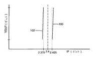
図4を参照して、シミュレーション結果がこの発明の比較器10のために示される。シミュレーションの間、電圧基準VCMは2.4ボルトの定電圧に固定されており、第1および第2の電源はそれぞれ接地と5.0ボルトとに設定されていた。入力信号INも2.4ボルトに設定され、入力信号IPの電圧はVCMに対して変動させられた。図4はシミュレーションのために選択された例示的なVCMと入力電圧とにおけるヒステリシスの幅を示す。曲線100で見られるように、IPが約25ミリボルト(mV)だけINを超えると、VOUTは比較的低い電圧値から比較的高い電圧値へ(すなわち0ボルトから5ボルトへ)の遷移を始める。曲線100は、好ましい設計の結果である急速な出力スルーレートを示す急勾配の線として示される。加えて、曲線102はIPがINより僅かに低く減じられた後でさえも5ボルトのままに留まることを示す。しかしながら、一旦IPがINより25mVだけ少なくなると、VOUTは示されるように5ボルトから0ボルトへの遷移を始める。
【0028】
図5を参照すると、VOUTの移動点における過渡分析が示される。曲線104で示されるようにIPがINより25mV高くなると、VOUTは時間T1で高いレベルへ遷移する。過渡正弦曲線に従って、曲線106で示されるようにINより下の信号IPの逆バイアスが、VOUTを時間T2で低いレベルへ遷移させる。その反対に、曲線108は入力信号INが初めは入力信号IPより下に逸れ、次に逆転して入力信号IPより大きくなるように逸れる場合に生じる反対の結果を示す。過渡分析は、一旦差動入力電圧がヒステリシス値すなわち25mVを超えたときの出力スルーレートの急速な応答を示す。差動入力信号が変動して(これはノイズにより起こる可能性がある)、25mVのヒステリシスレベルより低くなった場合、VOUTは遷移せず、望ましくないチャター信号を生じることもない。
【0029】
この発明は、バイポーラまたはMOS、p−チャネルが優勢のものまたはn−チャネルが優勢のもの、もしくはエンハンスメントが優勢のものまたはデプリーションが優勢のもののいずれのタイプでもよい数多くのタイプのトランジスタでの応用が可能であると信じられていることは、この開示の利益を受ける当業者には認識されるであろう。さらに、示されかつ説明されたこの発明の形式は現在好ましいとされる実施例として受け取られるべきであるということも理解されたい。様々な変形および変更が特許請求の範囲で述べられるこの発明の精神および範囲から逸脱することなく行なわれてよい。例示的な変形は、比較器の各段の電流吸込と反対のものとして電流源を用いるものであるかもしれない。さらに、電流吸込は定電流装置の各々のための電流源の代わりに用いられてもよい。さらに、ユーザの要求と特定の出力の応用とに応じてバッファ回路は用いられてもよいし用いられなくてもよい。前掲の特許請求の範囲はそのような変形および変更のすべてを包含するものとして解釈されるべく意図されている。
【図面の簡単な説明】
【図1】この発明による比較器回路のブロック図である。
【図2】この発明による比較器回路の一実施例の回路図である。
【図3】この発明による比較器回路の別の実施例の回路図である。
【図4】この発明に従って入力電圧対出力電圧の関数としてのヒステリシス幅を表わすグラフ図である。
【図5】この発明に従って基準電圧(VCM)に対しての入力電圧の関数としてのヒステリシス移動点の過渡分析を表わすグラフ図である。
【符号の説明】
10 比較器回路
12 主要差動増幅器段
14 ヒステリシス差動増幅器段
16 電圧バイアス発生器
18 定電流装置
20 定電流装置
22 カスコード装置および電流ミラー回路[0001]
FIELD OF THE INVENTION
The present invention relates to electronic circuits, and more particularly to a comparator circuit for comparing two input signals to generate a resulting output signal.
[0002]
[Background of related technology]
Comparator circuits used to compare two input signals are well known. In operating in the non-linear range, the comparator provides digital output voltage information corresponding to the difference between the input voltages. For example, if the input voltage provided to the non-inverting input is greater than the voltage provided to the inverting input, a relatively large output signal will be generated. Conversely, if the input voltage to the non-inverting input is lower than the input voltage to the inverting input, a relatively low output voltage will be generated. Thus, the comparator functions to compare the two input signals and generate a digital output based on the comparison.
[0003]
Most comparator circuits include at least two stages of operation. For example, a typical comparator uses a differential amplifier or differential transistor pair at the input stage of operation and multiple loads / buffers at the output stage. The amplifier and load circuit are biased from a constant current source and a voltage reference, typically generated in the same monolithic circuit as that of the comparator. By integrating the reference voltage device and the constant current source on the same silicon chip as the comparator, fewer package leads are required, i.e. power need not be drawn from outside the chip. Moreover, the operation of each component with fairly uniform processing parameters occurring over the substrate surface due to the integration is ensured.
[0004]
A problem often encountered with many conventional comparators is the detrimental effect of noise on the input signal that feeds the comparator. For example, if one input slightly exceeds the other due to noise, the output may be inadvertently triggered to the opposite digital value. Inadvertent triggering of the output due to rapid and slight fluctuations in the noise of the input signal will occur quickly and continuously. The presence of such fluctuations in the output of the comparator caused by input noise is sometimes referred to as "chatter".
[0005]
In attempting to overcome the chatter problem, many comparators use a hysteretic feedback loop from the output of the comparator to the input amplifier stage. A comparator circuit using a feedback hysteresis loop is described in U.S. Pat. No. 4,670,671. No. 4,670,671 describes a comparator circuit having two separate differential amplifiers, one amplifier receiving feedback information from the output of the comparator and the other amplifier receiving an input signal. . The device of Patent No. 4,670,671 guarantees that the output will not change unless one input signal exceeds the other input signal by a hysteresis value. As long as the noise peak at one input does not exceed the other input by a hysteresis value, the output of the comparator will not inadvertently toggle or chatter.
[0006]
The comparator of US Pat. No. 4,670,671 is primarily designed to use relatively little power while providing hysteretic feedback during high speed operation. As such, each differential amplifier (feedback differential amplifier and input differential amplifier) of Patent No. 4,670,671 requires a pair of feedback current mirrors or loads. While these loads provide high speed operation with low power consumption, each load must use three transistors interconnected with positive and negative driver circuits. Including separate loads and drivers increases the complexity of the device, requiring a large number of transistors and their associated interconnect routing. Adding transistors and routing only increases the cost of manufacturing monolithic devices and reduces the reliability of the devices.
[0007]
Summary of the Invention
Most of the problems outlined above are solved by the comparator of the present invention. That is, the comparator circuit described herein uses a single load circuit instead of the multiple load circuits often found in previous designs. Specifically, a single load circuit provided in the folded cascode device and the current mirror circuit includes a portion of a single suction and discharge output stage for the device of the present invention. The folded cascode device and the current mirror circuit receive parallel inputs from both the feedback (or hysteresis) differential amplifier and the input (or primary) differential amplifier. By connecting each differential amplifier pair of transistors in parallel between a constant current device and a cascode device, it is necessary to provide the operation of the present invention with relatively few active devices and their associated interconnects. Is a single load circuit. Instead of requiring four separate feedback current mirror loads (each load includes three transistors) and two separate drivers (positive and negative drivers) as shown in US Pat. No. 4,670,671. The present invention only requires a single shared current mirror load and a pair of cascode devices.
[0008]
Broadly, the present invention contemplates an improved comparator circuit having fewer active devices and associated interconnects. This comparator therefore occupies less silicon space and is more reliable to operate at lower cost of manufacture. The comparator includes a pair of current devices, and further includes a cascode device and a current mirror coupled to receive a first portion of current from each current device. A pair of differential transistors are coupled to receive a pair of input signals and also receive a second portion of the current from each current device. A pair of hysteresis transistors are coupled in parallel with the differential transistors to receive a third portion of the current from each current device. The output voltage generated from the cascode device and the current mirror circuit can be changed in response to a change in the relative magnitude of the first, second and third portions of the current.
[0009]
The present invention also contemplates a comparator circuit for comparing a pair of input signals. The improved comparator circuit described herein includes first and second current devices, each current device adapted to generate a constant current equal to the current generated by the other current device. The cascode device and the current mirror circuit are coupled to the first and second current devices such that the cascode device and the current mirror establish a suction and discharge output stage for delivering the output of the comparator. First and second conductive paths are respectively coupled between the cascode device and the current mirror circuit and the first and second current devices. The first conductive path is changed by the output of the comparator, and the second conductive path is changed by the variable reference voltage. The third and fourth conductive paths are coupled in parallel with the first and second conductive paths, respectively. The third conductive path is changed with one input signal of the input signal pair, and the fourth conductive path is changed with the other input signal of the input signal pair. Increasing the voltage of one input signal to a higher hysteresis value than the other input signal results in an imbalance in the sink and discharge currents in the output stage.
[0010]
The cascode device and current mirror circuit of the present invention do not require many active devices or transistors. Specifically, the cascode device and the current mirror circuit include first and second cascode transistors having one end of a conductive path connected to the first and second current devices, respectively. The four-transistor current mirror is connected between the cascode transistor and the first power supply, and the output node is connected between the second cascode transistor and the two series-connected transistors of the four-transistor current mirror.
[0011]
The present invention further contemplates a method for comparing a pair of input signals. The method includes providing a pair of constant value current devices and drawing a first portion of the current from each current device through a cascode device and a current mirror circuit. A second portion of the current is drawn from the current device through a pair of main differential transistors adapted to receive a pair of input signals. A third portion of the current is drawn from each current device via a pair of hysteretic differential transistors coupled to receive a reference voltage and an output voltage from the output of the comparator. The output voltage is generated by sinking and discharging current through the cascode device and the current mirror circuit, and then the output is fed back to one input of the hysteresis differential transistor pair. The output voltage changes in response to a change in the relative magnitude of the first, second, and third portions of the current. Digital changes in the output voltage occur when the relative magnitude of the current portion changes during the period when the voltage of one input signal exceeds the voltage of the other input signal by a certain amount of hysteresis.
[0012]
Other objects and advantages of the present invention will become apparent upon reading the following detailed description and referring to the accompanying drawings.
[0013]
While the invention is susceptible to various modifications and alternative forms, specific embodiments thereof have been shown by way of example in the drawings and will be described in detail below. However, the drawings and description thereof are not intended to limit the invention to the particular form disclosed, but, on the contrary, fall within the spirit and scope of the invention as defined by the appended claims. It is to be understood that the intent is to cover all variations, equivalents, and alternatives included.
[0014]
DETAILED DESCRIPTION OF THE INVENTION
Turning now to the drawings, FIG. 1 shows a block diagram of an
[0015]
A well-designed and well-known type of
[0016]
The third stage or cascode device and
[0017]
Referring to FIG. 2, a circuit diagram of one embodiment of the
[0018]
Coupled in parallel with
[0019]
Cascode device and
[0020]
The transistors found throughout the
[0021]
[0022]
If VOUT is at a relatively high voltage level,
[0023]
The amount of hysteresis voltage can be adjusted by changing the bias current in
[0024]
Referring to FIG. 3, there is shown an alternative embodiment of
[0025]
Shown in FIG. 3 is a parallel coupled
[0026]
The embodiment illustrated in FIG. 3 operates similarly to that shown in FIG. That is, VOUT is fed back to the hysteresis stage, thereby providing a subsequent transition of the output when a hysteresis differential input voltage occurs. Instead of sinking current from the current source transistors as in the embodiment of FIG. 2, stages 12 and 14 and circuit 22 (shown in FIG. 3) are in a relative proportion to the input signal difference and the current state of VOUT. A current is discharged to the
[0027]
Referring to FIG. 4, simulation results are shown for the
[0028]
Referring to FIG. 5, a transient analysis at the moving point of VOUT is shown. When IP rises 25 mV above IN as shown by
[0029]
The invention finds application in many types of transistors, which may be bipolar or MOS, either p-channel dominant or n-channel dominant, or enhancement dominant or depletion dominant. What is believed to be possible will be appreciated by those skilled in the art having the benefit of this disclosure. It is further to be understood that the forms of the invention shown and described are to be taken as the presently preferred embodiments. Various changes and modifications may be made without departing from the spirit and scope of the invention, which is set forth in the following claims. An exemplary variation might be to use a current source as the opposite of the current sink for each stage of the comparator. Furthermore, current sinks may be used instead of current sources for each of the constant current devices. Further, buffer circuits may or may not be used depending on the needs of the user and the particular output application. The following claims are intended to be construed as including all such variations and modifications.
[Brief description of the drawings]
FIG. 1 is a block diagram of a comparator circuit according to the present invention.
FIG. 2 is a circuit diagram of one embodiment of a comparator circuit according to the present invention.
FIG. 3 is a circuit diagram of another embodiment of the comparator circuit according to the present invention.
FIG. 4 is a graph illustrating hysteresis width as a function of input voltage versus output voltage in accordance with the present invention.
FIG. 5 is a graph illustrating a transient analysis of a hysteresis shift point as a function of input voltage with respect to a reference voltage (VCM) in accordance with the present invention.
[Explanation of symbols]
10. Comparator circuit
12 Main differential amplifier stages
14. Hysteresis differential amplifier stage
16 Voltage bias generator
18 Constant current device
20 Constant current device
22 Cascode device and current mirror circuit
Claims (18)
Translated fromJapanese前記1対の電流装置の各々から前記それぞれの電流の第1の部分を受け取る1対の吸込および吐出し電流経路を有し、前記1対の吸込および吐出し電流経路の一方から出力電圧を生成するように構成されるカスコード装置および電流ミラー回路と、
1対の入力信号を受け取りかつ、前記1対の入力信号に応じて前記1対の電流装置の各々から前記それぞれの電流の第2の部分を受け取るように構成される1対の差動トランジスタと、
前記1対の差動トランジスタと並列に結合されて、前記1対の電流装置の各々から前記それぞれの電流の第3の部分を受け取るように構成される1対のヒステリシストランジスタとを含み、
前記1対の差動トランジスタおよび前記1対のヒステリシストランジスタは、前記1対の電流装置と前記カスコード装置および電流ミラー回路との間の電流経路と並列に結合され、
前記1対のヒステリシストランジスタの第1の入力は前記出力電圧と結合され、前記1対のヒステリシストランジスタの第2の入力は基準電圧と結合され、
前記カスコード装置および電流ミラー回路は、前記それぞれの電流の前記第1、前記第2、および前記第3の部分の相対的な大きさの変化に応答して前記出力電圧を変化させることができる、比較器回路。A pair of current devices, each generating a respective current;
Apair of sink and discharge current paths for receiving afirst portion of the respective current from each of the pair of current devices,and generating an output voltage from one of the pair of suction and discharge current paths; A cascode device and a current mirror circuit configured to
A pair of differential transistors configured to receive a pair of input signals and to receive a second portion of the respective current from each of the pair of current devices in response to the pair of input signals; ,
A pair of hysteresis transistors coupled in parallel with the pair of differential transistors and configured to receive a third portion of the respective current from each of the pair of current devices;
The pair of differential transistors and the pair of hysteresis transistors are coupled in parallel with a current path between the pair of current devices and the cascode device and current mirror circuit;
A first input of the pair of hysteresis transistors is coupled to the output voltage; a second input of the pair of hysteresis transistors is coupled to a reference voltage;
The cascode devices and current mirrorcircuits can be changedthe first, the second, andthe output voltage in response to changes in the relative magnitudes of said third portion of said respective current , Comparator circuit.
定電流を生成する第1および第2の電流装置を含み、前記第1および第2の電流装置は、前記第1の電流装置によって生成される第1の電流が前記第2の電流装置によって生成される第2の電流と同程度となるように適合されており、さらに、
2つの吸込および吐出し電流経路と、これらの前記電流経路の1つに接続される出力とを有する単一のカスコード装置および電流ミラー回路と、
前記カスコード装置および電流ミラー回路と、前記第1および第2の電流装置との間にそれぞれ結合される第1および第2の導電経路と、
前記第1および第2の導電経路と並列に結合される第3および第4の導電経路とを含み、前記第3の導電経路を流れる電流は前記1対の入力信号のうちの第1の入力信号によって変えられ、前記第4の導電経路を流れる電流は前記1対の入力信号のうちの第2の入力信号によって変えられ、さらに、
前記第2の入力信号の電圧からヒステリシス値分増加された電圧と同程度の電圧まで前記第1の入力信号の電圧を等価的に高め、かつ、前記第1の導電経路を流れる電流を前記出力から送られた信号に応じて変えるとともに、前記第2の導電経路を流れる電流を可変の基準電圧に応じて変えるすることによって、前記吸込および吐出し電流経路に電流の不均衡をもたらすための手段を含む、比較器回路。A comparator circuit for comparing a pair of input signals,
A first current device for generating a constant current, wherein the first and second current devices generate a constant current by the first current device generated by the second current device; Is adapted to be comparable to the second current
A single cascode device and current mirror circuit having two suction and discharge current paths and an output connected to one of the current paths;
First and second conductive paths respectively coupled between the cascode device and the current mirror circuit, and the first and second current devices;
Third and fourth conductive paths coupled in parallel with the first and second conductive paths, wherein a current flowing through the third conductive path is a first input of the pair of input signals. And the current flowing through the fourth conductive path is changed by a second input signal of the pair of input signals, and
The voltage of the first input signal is equivalently increased to a voltage substantially equal to the voltage increased by the hysteresis value from the voltage of the second input signal, and the current flowing through the first conductive path is output to the output. Means for changing the current flowing through said second conductive path in response to a variable reference voltage and causing a current imbalance in said suction and discharge current paths. And a comparator circuit.
その導電経路の一端をそれぞれ前記第1および第2の電流装置に接続されている第1および第2のカスコードトランジスタと、
前記第1および第2のカスコードトランジスタと第1の電源との間に接続される、4トランジスタの電流ミラーとを含み、
前記出力は、前記第2のカスコードトランジスタと、前記電流ミラーに属する2つの直列に接続されたトランジスタ列の一方との間に接続される、請求項2に記載の比較器回路。The cascode device and the current mirror circuit,
First and second cascode transistors having one end of the conductive path connected to the first and second current devices, respectively;
A four-transistor current mirror connected between the first and second cascode transistors and a first power supply;
The comparator circuit according to claim2 , wherein the output is connected between the second cascode transistor and one of two serially connected transistor strings belonging to the current mirror.
定電流を生成する第1および第2の電流装置を含み、前記第1および第2の電流装置は、前記第1の電流装置によって生成される第1の電流が前記第2の電流装置によって生成される第2の電流と同程度となるように適合されており、さらに、
前記第1および第2の電流装置と第1の電源との間に配置されたカスコード装置および電流ミラー回路を含み、前記カスコード装置および電流ミラー回路は、
第1および第2のカスコードトランジスタを含み、前記第1および第2のカスコードトランジスタはそれぞれの導電経路を有し、かつ、前記それぞれ導電経路の一端はそれぞれ前記第1および第2の電流装置に接続され、さらに、前記カスコード装置および電流ミラー回路は、
前記第1および第2のカスコードトランジスタと第2の電源との間に接続される4トランジスタの電流ミラーと、
前記第2のカスコードトランジスタと前記電流ミラーに属する2つの直列に接続されたトランジスタ列の一方との間に接続される出力とを含み、
前記比較器回路は、さらに、
前記カスコード装置および電流ミラー回路と前記第1および第2の電流装置との間でそれぞれ結合される第1および第2の導電経路と、
前記第1および第2の導電経路と並列に結合される第3および第4の導電経路とを含み、前記第3の導電経路を流れる電流は前記1対の入力信号のうちの第1の入力信号によって変えられ、前記第4の導電経路を流れる電流は前記1対の入力信号のうちの第2の入力信号によって変えられ、さらに、
前記第2の入力信号の電圧からヒステリシス値分増加された電圧と同程度の電圧まで前記第1の入力信号の電圧を等価的に高め、かつ、前記第1の導電経路を流れる電流を前記出力から送られた信号に応じて変えるとともに、前記第2の導電経路を流れる電流を可変の基準電圧に応じて変えることによって、前記第1および第2のカスコードトランジスタの間に電流の不均衡をもたらすための手段を含む、比較器回路。A comparator circuit for comparing a pair of input signals,
A first current device for generating a constant current, wherein the first and second current devices generate a constant current by the first current device generated by the second current device; Is adapted to be comparable to the second current
A cascode device and a current mirror circuit disposed between the first and second current devices and a first power supply;
A first and a second cascode transistor include first and second cascode transistors, each of the first and second cascode transistors has a respective conductive path, and one end of the respective conductive path is connected to the first and second current devices, respectively. Further, the cascode device and the current mirror circuit,
A four-transistor current mirror connected between the first and second cascode transistors and a second power supply;
An output connected between the second cascode transistor and one of two serially connected transistor strings belonging to the current mirror;
The comparator circuit further includes:
First and second conductive paths respectively coupled between the cascode device and the current mirror circuit and the first and second current devices;
Third and fourth conductive paths coupled in parallel with the first and second conductive paths, wherein a current flowing through the third conductive path is a first input of the pair of input signals. And the current flowing through the fourth conductive path is changed by a second input signal of the pair of input signals, and
The voltage of the first input signal is equivalently increased to a voltage substantially equal to the voltage increased by the hysteresis value from the voltage of the second input signal, and the current flowing through the first conductive path is output to the output. And a current imbalance between the first and second cascode transistors by changing the current flowing through the second conductive path in response to a variable reference voltage while changing the current through the second conductive path. A comparator circuit, including means for:
1対の一定値の電流装置を設けるステップと、
前記電流装置の各々からの電流の第1の部分を、カスコード装置および電流ミラー回路を介して引き出すステップとを含み、前記カスコード装置および電流ミラー回路は、各前記電流装置からの電流の前記第1の部分を受け取る1対の吸込および吐出し電流経路を有し、前記1対の吸込および吐出し電流経路の一方から出力電圧を生成するように構成され、
前記電流装置の各々からの前記電流の第2の部分を、前記1対の入力信号をそれぞれの入力において受け取るように構成された1対の差動トランジスタを介して引き出すステップと、
前記電流装置の各々からの前記電流の第3の部分を、基準電圧および前記出力電圧をそれぞれの入力において受け取るように構成された1対のヒステリシストランジスタを介して引き出すステップと、
電流の前記第1、第2および第3の部分の相対的な大きさの変化に応答して、前記カスコード装置および電流ミラー回路からの前記出力電圧を変化させるステップとを含む、方法。A method for comparing a pair of input signals, the method comprising:
Providing a pair of constant value current devices;
Extracting a first portion of the current from each of the current devices via a cascode device and a current mirror circuit, the cascode device and the current mirror circuit providing the first portion of thecurrent from each of the current devices. Having a pair of suction and discharge current paths for receiving a portion of the pair, and configured to generate an output voltage from one of the pair of suction and discharge current paths ;
Drawing a second portion of the current from each of the current devices through a pair of differential transistors configured to receive the pair of input signals atrespective inputs ;
Extracting a third portion of the current from each of the current devices through a pair of hysteresis transistors configured to receive a reference voltageand the output voltageat respective inputs ;
It said first current, in response to changes in the relative magnitudes of the second and third portions, and a step of Ruchanging the output voltagefrom said cascode devices and current mirror circuit, method.
Applications Claiming Priority (2)
| Application Number | Priority Date | Filing Date | Title |
|---|---|---|---|
| US964781 | 1992-10-22 | ||
| US07/964,781US5446396A (en) | 1992-10-22 | 1992-10-22 | Voltage comparator with hysteresis |
Publications (2)
| Publication Number | Publication Date |
|---|---|
| JPH06204820A JPH06204820A (en) | 1994-07-22 |
| JP3574162B2true JP3574162B2 (en) | 2004-10-06 |
Family
ID=25508990
Family Applications (1)
| Application Number | Title | Priority Date | Filing Date |
|---|---|---|---|
| JP26055193AExpired - Fee RelatedJP3574162B2 (en) | 1992-10-22 | 1993-10-19 | Comparator circuit for comparing a pair of input signals and method therefor |
Country Status (4)
| Country | Link |
|---|---|
| US (1) | US5446396A (en) |
| EP (1) | EP0594305B1 (en) |
| JP (1) | JP3574162B2 (en) |
| DE (1) | DE69317350D1 (en) |
Families Citing this family (25)
| Publication number | Priority date | Publication date | Assignee | Title |
|---|---|---|---|---|
| EP0681293B1 (en)* | 1994-05-03 | 2001-03-28 | STMicroelectronics S.r.l. | Sense amplifier with hysteresis |
| US5587674A (en)* | 1994-12-30 | 1996-12-24 | Sgs-Thomson Microelectronics, Inc. | Comparator with built-in hysteresis |
| EP0779711A3 (en)* | 1995-12-14 | 1999-05-12 | STMicroelectronics, Inc. | A timer circuit |
| US5668486A (en)* | 1996-06-21 | 1997-09-16 | Brehmer; Geoffrey E. | Strobed comparator for a large common mode range |
| US6307415B1 (en) | 1996-09-20 | 2001-10-23 | Stmicroelectronics, Inc. | Hysteresis circuit |
| US6271715B1 (en) | 1998-02-27 | 2001-08-07 | Maxim Integrated Products, Inc. | Boosting circuit with supply-dependent gain |
| US5945852A (en)* | 1998-03-31 | 1999-08-31 | Motorola, Inc. | CMOS comparator output circuit with high gain and hysteresis |
| US6377084B2 (en) | 1999-02-22 | 2002-04-23 | Micron Technology, Inc. | Pseudo-differential amplifiers |
| US6307405B2 (en)* | 1999-04-27 | 2001-10-23 | Micron Technology, Inc. | Current sense amplifier and current comparator with hysteresis |
| US6288575B1 (en)* | 1999-08-24 | 2001-09-11 | Micron Technology, Inc. | Pseudo-differential current sense amplifier with hysteresis |
| JP3687545B2 (en)* | 2001-02-05 | 2005-08-24 | セイコーエプソン株式会社 | Comparator circuit |
| US6614279B2 (en)* | 2001-08-29 | 2003-09-02 | Intel Corporation | Clock receiver circuit for on-die salphasic clocking |
| DE10327284B4 (en)* | 2003-06-17 | 2005-11-03 | Infineon Technologies Ag | Test device for memory |
| US6970022B1 (en)* | 2003-09-18 | 2005-11-29 | Lattice Semiconductor Corporation | Controlled hysteresis comparator with rail-to-rail input |
| US7106104B2 (en)* | 2003-10-30 | 2006-09-12 | International Business Machines Corporation | Integrated line driver |
| FR2889875B1 (en)* | 2005-08-22 | 2007-11-30 | Atmel Nantes Sa Sa | HYSTERESIS COMPARATOR OF INPUT VOLTAGES AND CORRESPONDING ELECTRONIC CIRCUIT. |
| US7292083B1 (en)* | 2006-04-18 | 2007-11-06 | Etron Technology, Inc. | Comparator circuit with Schmitt trigger hysteresis character |
| US7532041B2 (en)* | 2006-12-20 | 2009-05-12 | Texas Instruments Incorporated | Systems and methods for hysteresis control in a comparator |
| JP5584196B2 (en)* | 2009-03-05 | 2014-09-03 | パナソニック インテレクチュアル プロパティ コーポレーション オブ アメリカ | Distance measuring device, distance measuring method, program, and integrated circuit |
| US8310279B2 (en)* | 2009-05-18 | 2012-11-13 | Qualcomm, Incorporated | Comparator with hysteresis |
| US8203370B2 (en)* | 2009-06-30 | 2012-06-19 | Silicon Laboratories Inc. | Schmitt trigger with gated transition level control |
| US8930591B2 (en) | 2012-06-30 | 2015-01-06 | Silicon Laboratories Inc. | Apparatus for improved signal communication in electronic circuitry and associated methods |
| US9654086B1 (en) | 2016-01-11 | 2017-05-16 | Globalfoundries Inc. | Operational amplifier with current-controlled up or down hysteresis |
| TWI632776B (en)* | 2016-08-18 | 2018-08-11 | 瑞昱半導體股份有限公司 | Phase interpolator |
| FR3083654B1 (en) | 2018-07-05 | 2021-04-02 | St Microelectronics Rousset | POLARIZATION METHOD OF THE OUTPUTS OF A FOLDED CASCODE STAGE OF A COMPARATOR AND CORRESPONDING COMPARATOR |
Family Cites Families (11)
| Publication number | Priority date | Publication date | Assignee | Title |
|---|---|---|---|---|
| US4670671A (en)* | 1986-02-19 | 1987-06-02 | Advanced Micro Devices, Inc. | High speed comparator having controlled hysteresis |
| US4677315A (en)* | 1986-07-28 | 1987-06-30 | Signetics Corporation | Switching circuit with hysteresis |
| US4717838A (en)* | 1986-11-14 | 1988-01-05 | National Semiconductor Corporation | High input impedance, high gain CMOS strobed comparator |
| US4808848A (en)* | 1988-03-07 | 1989-02-28 | Motorola, Inc. | Comparator circuit |
| GB2219162B (en)* | 1988-05-28 | 1992-06-10 | Stc Plc | Amplifier circuit |
| US4874969A (en)* | 1988-06-08 | 1989-10-17 | National Semiconductor Corporation | High speed CMOS comparator with hysteresis |
| US4940907A (en)* | 1989-01-19 | 1990-07-10 | Ford Motor Company | Precision CMOS comparator with hysteresis |
| EP0417334B1 (en)* | 1989-09-11 | 1993-12-29 | Siemens Aktiengesellschaft | Latch circuit with switching hysterisis |
| US5117199A (en)* | 1991-03-27 | 1992-05-26 | International Business Machines Corporation | Fully differential follower using operational amplifier |
| US5289054A (en)* | 1992-03-24 | 1994-02-22 | Intel Corporation | Fast electronic comparator |
| US5362994A (en)* | 1992-10-13 | 1994-11-08 | Winbond Electronics North America Corporation | Comparator with controlled hysteresis |
- 1992
- 1992-10-22USUS07/964,781patent/US5446396A/ennot_activeExpired - Lifetime
- 1993
- 1993-09-22DEDE69317350Tpatent/DE69317350D1/ennot_activeExpired - Lifetime
- 1993-09-22EPEP93307482Apatent/EP0594305B1/ennot_activeExpired - Lifetime
- 1993-10-19JPJP26055193Apatent/JP3574162B2/ennot_activeExpired - Fee Related
Also Published As
| Publication number | Publication date |
|---|---|
| JPH06204820A (en) | 1994-07-22 |
| DE69317350D1 (en) | 1998-04-16 |
| EP0594305A1 (en) | 1994-04-27 |
| EP0594305B1 (en) | 1998-03-11 |
| US5446396A (en) | 1995-08-29 |
Similar Documents
| Publication | Publication Date | Title |
|---|---|---|
| JP3574162B2 (en) | Comparator circuit for comparing a pair of input signals and method therefor | |
| US4853654A (en) | MOS semiconductor circuit | |
| US7145364B2 (en) | Self-bypassing voltage level translator circuit | |
| US6118318A (en) | Self biased differential amplifier with hysteresis | |
| JP3920236B2 (en) | Differential amplifier | |
| US4394587A (en) | CMOS Differential comparator with hysteresis | |
| JPH05243867A (en) | Comparator | |
| US7432762B2 (en) | Circuit having enhanced input signal range | |
| US4598215A (en) | Wide common mode range analog CMOS voltage comparator | |
| US4410813A (en) | High speed CMOS comparator circuit | |
| US5929679A (en) | Voltage monitoring circuit capable of reducing power dissipation | |
| US7391825B2 (en) | Comparator circuit having reduced pulse width distortion | |
| US5847581A (en) | Low power CMOS precision input receiver with integrated reference | |
| US6373291B1 (en) | Pass transistor logic circuit for reducing power consumption | |
| US6281731B1 (en) | Control of hysteresis characteristic within a CMOS differential receiver | |
| US5977800A (en) | Differential MOS current-mode logic circuit having high gain and fast speed | |
| US7068074B2 (en) | Voltage level translator circuit | |
| US20040155689A1 (en) | Differential input receiver with hysteresis | |
| KR20040023837A (en) | Differential amplification type input buffer in semiconductor device | |
| JPH11103227A (en) | Output amplitude adjusting circuit | |
| US6836155B2 (en) | Current sense amplifier | |
| US20050134364A1 (en) | Reference compensation circuit | |
| US6356121B1 (en) | Very low-power comparison device | |
| US5710516A (en) | Input logic signal buffer circuits | |
| US6529036B1 (en) | Low noise, reduced swing differential output buffer design |
Legal Events
| Date | Code | Title | Description |
|---|---|---|---|
| A02 | Decision of refusal | Free format text:JAPANESE INTERMEDIATE CODE: A02 Effective date:20040203 | |
| A521 | Written amendment | Free format text:JAPANESE INTERMEDIATE CODE: A523 Effective date:20040506 | |
| A911 | Transfer to examiner for re-examination before appeal (zenchi) | Free format text:JAPANESE INTERMEDIATE CODE: A911 Effective date:20040511 | |
| TRDD | Decision of grant or rejection written | ||
| A01 | Written decision to grant a patent or to grant a registration (utility model) | Free format text:JAPANESE INTERMEDIATE CODE: A01 Effective date:20040601 | |
| A61 | First payment of annual fees (during grant procedure) | Free format text:JAPANESE INTERMEDIATE CODE: A61 Effective date:20040701 | |
| R150 | Certificate of patent or registration of utility model | Free format text:JAPANESE INTERMEDIATE CODE: R150 | |
| FPAY | Renewal fee payment (event date is renewal date of database) | Free format text:PAYMENT UNTIL: 20070709 Year of fee payment:3 | |
| FPAY | Renewal fee payment (event date is renewal date of database) | Free format text:PAYMENT UNTIL: 20080709 Year of fee payment:4 | |
| FPAY | Renewal fee payment (event date is renewal date of database) | Free format text:PAYMENT UNTIL: 20080709 Year of fee payment:4 | |
| FPAY | Renewal fee payment (event date is renewal date of database) | Free format text:PAYMENT UNTIL: 20090709 Year of fee payment:5 | |
| FPAY | Renewal fee payment (event date is renewal date of database) | Free format text:PAYMENT UNTIL: 20090709 Year of fee payment:5 | |
| FPAY | Renewal fee payment (event date is renewal date of database) | Free format text:PAYMENT UNTIL: 20100709 Year of fee payment:6 | |
| FPAY | Renewal fee payment (event date is renewal date of database) | Free format text:PAYMENT UNTIL: 20110709 Year of fee payment:7 | |
| FPAY | Renewal fee payment (event date is renewal date of database) | Free format text:PAYMENT UNTIL: 20110709 Year of fee payment:7 | |
| FPAY | Renewal fee payment (event date is renewal date of database) | Free format text:PAYMENT UNTIL: 20120709 Year of fee payment:8 | |
| LAPS | Cancellation because of no payment of annual fees |