JP3572247B2 - Gas inlet pipe for semiconductor heat treatment furnace - Google Patents
Gas inlet pipe for semiconductor heat treatment furnaceDownload PDFInfo
- Publication number
- JP3572247B2 JP3572247B2JP2000307323AJP2000307323AJP3572247B2JP 3572247 B2JP3572247 B2JP 3572247B2JP 2000307323 AJP2000307323 AJP 2000307323AJP 2000307323 AJP2000307323 AJP 2000307323AJP 3572247 B2JP3572247 B2JP 3572247B2
- Authority
- JP
- Japan
- Prior art keywords
- tube
- sic
- cvd
- quartz glass
- heat treatment
- Prior art date
- Legal status (The legal status is an assumption and is not a legal conclusion. Google has not performed a legal analysis and makes no representation as to the accuracy of the status listed.)
- Expired - Fee Related
Links
- 239000004065semiconductorSubstances0.000titleclaimsdescription37
- 238000010438heat treatmentMethods0.000titleclaimsdescription27
- VYPSYNLAJGMNEJ-UHFFFAOYSA-NSilicium dioxideChemical compoundO=[Si]=OVYPSYNLAJGMNEJ-UHFFFAOYSA-N0.000claimsdescription46
- 230000002093peripheral effectEffects0.000claimsdescription12
- 230000003746surface roughnessEffects0.000claimsdescription11
- 235000012431wafersNutrition0.000description17
- 239000000463materialSubstances0.000description12
- 238000004519manufacturing processMethods0.000description11
- 238000000034methodMethods0.000description11
- OKTJSMMVPCPJKN-UHFFFAOYSA-NCarbonChemical compound[C]OKTJSMMVPCPJKN-UHFFFAOYSA-N0.000description7
- 229910052799carbonInorganic materials0.000description7
- 239000002245particleSubstances0.000description6
- 238000005229chemical vapour depositionMethods0.000description5
- 229910021420polycrystalline siliconInorganic materials0.000description5
- 229920005591polysiliconPolymers0.000description5
- XUIMIQQOPSSXEZ-UHFFFAOYSA-NSiliconChemical compound[Si]XUIMIQQOPSSXEZ-UHFFFAOYSA-N0.000description4
- 238000002347injectionMethods0.000description4
- 239000007924injectionSubstances0.000description4
- 229910052710siliconInorganic materials0.000description4
- 239000010703siliconSubstances0.000description4
- 230000003028elevating effectEffects0.000description3
- 230000005484gravityEffects0.000description3
- 239000010453quartzSubstances0.000description3
- 238000005406washingMethods0.000description3
- ZOXJGFHDIHLPTG-UHFFFAOYSA-NBoronChemical compound[B]ZOXJGFHDIHLPTG-UHFFFAOYSA-N0.000description2
- 229910052796boronInorganic materials0.000description2
- 238000001816coolingMethods0.000description2
- 230000003670easy-to-cleanEffects0.000description2
- 238000007789sealingMethods0.000description2
- 230000008646thermal stressEffects0.000description2
- ZOKXTWBITQBERF-UHFFFAOYSA-NMolybdenumChemical compound[Mo]ZOKXTWBITQBERF-UHFFFAOYSA-N0.000description1
- OAICVXFJPJFONN-UHFFFAOYSA-NPhosphorusChemical compound[P]OAICVXFJPJFONN-UHFFFAOYSA-N0.000description1
- 239000002253acidSubstances0.000description1
- 238000000137annealingMethods0.000description1
- 238000005452bendingMethods0.000description1
- 238000004140cleaningMethods0.000description1
- 239000011248coating agentSubstances0.000description1
- 238000000576coating methodMethods0.000description1
- 238000000151depositionMethods0.000description1
- 238000010586diagramMethods0.000description1
- 239000000428dustSubstances0.000description1
- 230000000694effectsEffects0.000description1
- 239000011521glassSubstances0.000description1
- 238000009434installationMethods0.000description1
- 238000005304joiningMethods0.000description1
- 229910052750molybdenumInorganic materials0.000description1
- 239000011733molybdenumSubstances0.000description1
- 230000001590oxidative effectEffects0.000description1
- 229910052698phosphorusInorganic materials0.000description1
- 239000011574phosphorusSubstances0.000description1
- 238000000926separation methodMethods0.000description1
- 239000000758substrateSubstances0.000description1
- 238000010998test methodMethods0.000description1
- WFKWXMTUELFFGS-UHFFFAOYSA-NtungstenChemical compound[W]WFKWXMTUELFFGS-UHFFFAOYSA-N0.000description1
- 229910052721tungstenInorganic materials0.000description1
- 239000010937tungstenSubstances0.000description1
- XLYOFNOQVPJJNP-UHFFFAOYSA-NwaterSubstancesOXLYOFNOQVPJJNP-UHFFFAOYSA-N0.000description1
Images


Landscapes
- Chemical Vapour Deposition (AREA)
Description
Translated fromJapanese【0001】
【発明の属する技術分野】
本発明は半導体熱処理炉用ガス導入管に係わり、特にその一部にCVD−SiC管を用いた半導体熱処理炉用ガス導入管に関する。
【0002】
【従来の技術】
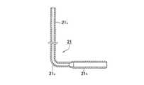
近年、半導体のLP−CVD、アニール等の熱処理工程は、縦型半導体熱処理炉を用いて行われている。この縦型半導体熱処理炉には、縦型に配置された炉芯管の処理空間に処理ガスを導入するためのガス導入管が設けられていた。図4に示すように、従来のガス導入管21は、純度、加工性に優れていることから石英ガラス製の管体でほぼL字形状をなし、炉芯管内に延伸する垂直部21vと、屈曲部21cと、炉芯管の底部近傍に配置される水平部21hを有している。
【0003】
そして、縦型半導体熱処理炉においては、縦型ボートの縦方向に配列された半導体ウェーハへの堆積膜の均一性を高めるために、導入管21を長くして、開口部を高い位置に設けた導入管21を、従来の高さを有する他の導入管と共に、配置するようになっている。
【0004】
このような縦型半導体熱処理炉は、単なるポリシリコンの堆積膜に用いるのみならず、より厳密な均一性を要求されるボロンやリンなどのドープドポリシリコン膜を半導体ウェーハ上に形成するのにも用いられる。
【0005】
このように、導入管21を長くすればする程、この導入管自身の外壁にも、堆積膜が多く堆積される。すると、従来の石英ガラス管であると、この石英ガラス管と堆積膜を形成する材料の熱膨張係数の違いから、外壁および内壁に堆積した堆積膜が部分的に剥がれるなどして、パーティクルの要因となり、半導体ウェーハの製造歩留を低下させていた。また、導入管21の使用後にHFなどを用いて洗浄して繰返し使用するが、洗浄時、石英ガラスが溶出し、その使用寿命を短縮する問題もある。
【0006】
そこで、この問題点を解消する方策として、特許第2990670号に記載されるように、CVD−SiC膜のみからなるL字状の導入管を検討した。この導入管の製造方法は、例えば、図5に示すように、炭素基材をL字状の円柱体22に加工した後に、3点支持して、CVD炉内に配置し、この外表面にCVD−SiCコートし、炉外で、炭素基材を焼き抜く方法で行われるが、このような方法によると、炭素円柱体22が撓むことで、ストレートな導入管を得にくいという問題がある。また、上記焼き抜きの前には、導入管の寸法を精度良くするために端部を加工する必要があるが、複雑形状であるため、高精度の加工が困難であるなどの問題がある。
【0007】
さらに、CVD−SiC膜のみからなる導入管において、炉芯管を貫通するチューブアダプタと当接する部分のシール性を高めるために、導入管の当該当接部を高精度に平坦化加工する必要があるが、この加工に多くの労力を要する。また、この導入管において、上述のように堆積膜が外壁および内壁にも堆積し、付着するために、これを酸洗浄によって、除去することで、繰返し使用されるが、L字状であるため、特に、角部内部の洗浄が容易でなく、堆積膜が完全に除去できず、パーティクルが発生する危険があった。
【0008】
【発明が解決しようとする課題】
そこで堆積した堆積膜の部分的剥離を防止することにより、パーティクルをなくし、半導体ウェーハの製造歩留を向上させ、さらに、製造が容易であり、使用時の洗浄が容易な導入管が要望されていた。
【0009】
本発明は上述した事情を考慮してなされたもので、特に、堆積した堆積膜の部分的剥離を防止することにより、パーティクルをなくし、半導体ウェーハの製造歩留を向上させ、さらに、製造が容易であり、使用時の洗浄が容易な導入管を提供することを目的とする。
【0010】
【課題を解決するための手段】
上記目的を達成するためになされた本願請求項1の発明は、L字状の石英ガラス管と、この石英ガラス管の一端に接合されたストレート状のCVD−SiC管とを有し、前記石英ガラス管は、その一端部に外周先細のテーパ部が形成され、このテーパ部が1/5〜1/15のテーパを有し、かつその屈曲部の管壁の肉厚は全周に亘り等しく、かつ、水平部の管壁の肉厚の1.2〜4.5倍であり、前記CVD−SiC管は、その一端部の内周先太のテーパ部が1/5〜1/15のテーパを有し、その内表面粗さがRa≦5μmであり、前記接合は、少なくともCVD−SiC管の一端部に形成されたテーパ部を石英ガラス管の一端部に嵌合することにより行われることを特徴とする半導体熱処理炉用ガス導入管であることを要旨としている。
【0011】
好適な一例では、前記石英ガラス管の外表面粗さがRaで2μm以上である。
【0014】
【発明の実施の形態】
本発明に係わる半導体熱処理炉用ガス導入管の実施形態について図面を参照して説明する。
【0015】
図1は縦型半導体熱処理炉1の概略図であり、この縦型半導体熱処理炉1は、全体的に円筒形状の炉芯管2を有している。この炉芯管2は下方に開口3を有し、この開口3からウェーハボート4に搭載された多数の半導体ウェーハWが出し入れされる構成になっている。炉芯管2は石英ガラスで構成されており、その内部に処理空間5が形成されている。
【0016】
処理空間5内には、ガス導入長管6とガス導入短管7が設けられており、所定の処理用ガスを処理空間5内に導入できるようになっている。
【0017】
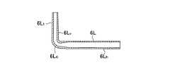
ガス導入長管6は、図2に示すようなL字状の石英ガラス管6Lと、図3に示すようなストレート状のCVD−SiC管6Sとで構成されている。
【0018】
石英ガラス管6Lは、炉芯管2に水平に配置される水平部6Lhと、90°の屈曲する屈曲部6Lcと、炉芯管2に垂直に配置される垂直部6Lvとで形成されている。石英ガラス管の一端部、すなわち、垂直部6Lvには外周先細のテーパ部6Ltが形成され、このテーパ部6Ltは1/5〜1/15のテーパを有している。また、屈曲部6Lcの管壁は、各垂直断面において肉厚が等しく、かつ、水平部6Lhの管壁の肉厚の1.2〜4.5倍である。
【0019】
このような屈曲部6Lcを有する石英ガラス管6Lとすることによって、ガス導入管をテーパ部に嵌合した場合にも、十分耐え得る強度が得られる。水平部6Lhの管壁の肉厚の4.5倍を超えると、かえって重量増加を招き好ましくない。
【0020】
CVD−SiC管6Sは次のようにして製造される。例えば、ストレートな円柱形状の炭素基材を用意し、一端部に外周先太のテーパ部が形成されるように外周加工し、しかる後、通常のCVD(Chemical vapor deposition)により、炭素基材上にSiCを0.7〜2.0mm堆積させる。さらに、長さ寸法合わせの加工を行なった後、酸化性雰囲気900℃で炭素基材の焼き抜きを行い、さらに、テーパ部内周面の研磨加工を行った後、洗浄を行うことにより製造される。このようにして製造されたCVD−SiC管6SはCVD−SiC膜のみで形成される。なお、基材としては、モリブデン、タングステン製のものを用いることもできる。
【0021】
このとき、CVD−SiC管6Sの内表面粗さがRa≦5μmに制御される。このように内表面粗さがRa≦5μmにすることにより、CVD−SiC管6Sと石英ガラス管6Lの嵌合部でのがたつきがなく、嵌合部の熱伝達も良くなり、SiCの高熱伝導性の特性を活かし、局部熱応力を緩和することができる。また、外表面粗さをRa≧2μmに制御するのが好ましい。これにより、CVD−SiC管6Sの外表面から例えばドープドポリシリコン膜が剥離し難くなり発生するダストを削減することができる。
【0022】
さらに、CVD−SiC管6Sの一端部には内周先太のテーパ部6Stが形成され、このテーパ部6Stも、上記垂直部6Lvのテーパ部6Ltと同様に1/5〜1/15のテーパを有しており、また、他端には処理ガス噴出口6Spが形成されている。
【0023】
ガス導入短管7も、図2に示すようなガス導入長管6の石英ガラス管6Lと同様の石英ガラス管7Lと、この石英ガラス管7Lの一端部に嵌合し、図3に示すようなガス導入長管6のCVD−SiC管6Sと同様のCVD−SiC管7Sとで構成され、他端には処理ガス噴出口7Spが設けられている。ただし、CVD−SiC管7Sの長さは、CVD−SiC管6Sの長さが約700〜1000mmであるのに対して、約100mmである。
【0024】
このように、石英ガラス管の一端部に形成された外周先細のテーパ部に一端部が内周先太のテーパ部を有するCVD−SiC管を上方より被せる(嵌合する)構造であるために、管内部にガス滞留が生じることもなく、内表面でのポリシリコン膜の付着がほとんど生じることがない。
【0025】
ガス導入長管6およびガス導入短管7は、各々炉芯管2を貫通するSUS製チューブアダプタ(水冷ジャケット)8、9に石英ガラス管6L、7Lを介して取り付けられ、さらに、チューブアダプタ8、9を介して、外部の処理ガス供給源(図示せず)に接続されている。このガス導入長管6およびガス導入短管7をチューブアダプタ8、9に取り付ける際、石英ガラス管6L、7Lを介して行うので、CVD−SiCに比べてはるかに加工し易い石英ガラスを加工すれば良く、その取り付け作業も容易になる。
【0026】
なお、10は昇降自在に設けられた昇降装置であり、11は昇降装置10に載置されたボートテーブルであり、このボートテーブル11には上記ウェーハボート4が載置される。また、12は炉芯管2を加熱するヒータ、13は処理ガスの排気口である。
【0027】
また、本発明のガス導入管においては、炉芯管を貫通するチューブアダプタと当接する部分が、表面が滑らかな通常の石英ガラスであるため、特別な外周面加工を行うこともなくシール性を高めることができる。
【0028】
次に本発明に係わる半導体熱処理炉用ガス導入管が設けられた縦型半導体熱処理炉を用いた半導体ウェーハの熱処理について説明する。
【0029】
半導体ウェーハWが搭載されたウェーハボート4を、昇降装置10に載置されたボートテーブル11に乗せて、ヒータ12により加熱された炉芯管2に収納する。しかる後、さらに炉芯管2内の温度を上げ、加熱されたボロンがドープされた処理ガスをガス導入長管6およびガス導入短管7から処理ガス噴出口6Sp、7Spを介して炉芯管2内に導入する。導入された処理ガスにより、シリコン膜を半導体ウェーハW上に堆積させ、その後、処理ガスを排気口13から排気する。
【0030】
この処理工程において、CVD−SiC管6S、7Sの外壁および内壁に処理ガスから生じるシリコン膜が堆積するが、CVD−SiC管6S、7S自身がCVD法により形成されたSiC(膜)材料(CVD−SiC)のみで形成されており、SiCの熱膨張係数と堆積したシリコン膜の熱膨張係数の差が大きくないので、ヒートサイクルにより、熱膨張係数の差から付着したシリコン膜の破断、部分的剥離を防止することにより、炉芯管2内のパーティクルを70%減じることができ、半導体ウェーハの製造歩留を向上させることができる。また、導入管6、7の使用後にHFなどを用いて洗浄して繰返し使用するが、洗浄時SiCは溶出せず、従来の石英ガラス製ガス導入管に比べ約20倍の長寿命化が図れる。
【0031】
また、石英ガラス管6L、7LとCVD−SiC管6S、7Sの接合は1/5〜1/15のテーパを有するテーパ部6Lt、6Stを用いた嵌合により行われる場合、CVD−SiC管6S、7Sの重力により気密かつ確実に接合され、さらに、取り外し時にも抜けが良く、分解時の破損事故なども防止できる。また、接合は熱膨張係数の差を有する石英ガラスとCVD−SiCの嵌合により行われるので、同一温度での熱膨張差により密着性が向上する。
【0032】
さらに、使用時、あるいは、搬送時など取扱い時に石英ガラス管6L、7Lが破損しても、石英ガラス管6L、7LまたはCVD−SiC管6S、7Sの破損側のみを交換すればよいので、経済的である。
【0033】
なお、上述した実施形態では、縦型半導体熱処理炉用ガス導入管について説明したが、本発明に係わる半導体熱処理炉用ガス導入管は、横型半導体熱処理炉用ガス導入管としても用いることができ、この場合には、CVD−SiC管の処理ガス噴出口近傍を支持する支持部材を別途設け、CVD−SiC管を安定化させるのが好ましい。
【0034】
【実施例】
(試験方法)
垂直部長さ45mmの石英L字インジェクションと、テーパまたはテーパ部内表面の表面粗さを変化させた長さ935mmのCVD−SiCインジェクションとをテーパ嵌合して950mmの高さのL字インジェクションを作製した。これらL字インジェクションの▲1▼テーパ嵌合の着脱時の作業性 ▲2▼嵌合個所の気密性
について調べた。
【0035】
(試験結果)
実施例1:テーパ1/4にした実施例1では、嵌合の際、SiCインジェクタの鉛直方向(縦型炉の場合)を向かず、炉芯管やボートにインジェクタ先端が接触してしまう可能性があり、また、鉛直方向から反れた場合、テーパ嵌合部からリークの可能性があることが確認された。
【0036】
実施例2:テーパ1/5にした実施例2では、嵌合した950mmインジェクタの先端が鉛直方向から反れる幅は、最大で1mmであった。また、350℃減圧下の使用においても、リークは検出されなかった。
【0037】
実施例3:テーパ1/10にした実施例3では、嵌合した950mmインジェクタの先端が鉛直方向から反れる幅は、最大で0.4mmであった。また、350℃減圧下の使用においても、リークは検出されなかった。
【0038】
実施例4:テーパ1/15にした実施例4では、嵌合した950mmインジェクタの先端が鉛直方向から反れる幅は、最大で0.05mmであった。また、350℃減圧下の使用においても、リークは検出されなかった。しかし、冷却後の分解時に、力を加えないと外れない状態になる場合もあったが、割れは見られなかった。
【0039】
実施例5:テーパ1/18にした実施例5では、容易に鉛直方向が出せるが、熱が加わったとき、熱膨張差による焼嵌(CTE外周材料>CTE内周材料の場合、加熱時に拡張した状態となったまま、これが冷却されると、外周材料が内周材料を圧縮すること)が発生し、強度の小さい石英インジェクタが抜けなくなったり、割れたりする可能性が高いことが確認された。
【0040】
実施例6:上記実施例2を用い、そのテーパ部内表面の表面粗さをRa=10mmとした実施例6では、350℃減圧下でインジェクタ内を通るガスのリークは検出されなかった。しかし、使用後の取り外し時にテーパ部にポリシリコンが付着する可能性が高いことが確認された。
【0041】
実施例7:上記実施例2、実施例3および実施例4を用い、そのテーパ部内表面の表面粗さをRa=5mmとした実施例7では、いずれのインジェクタ共、常温でも、350℃減圧下でもガスリークは検出されなかった。また、プロセスガスのテーパ部への回り込みも検出されなかった。
【0042】
【発明の効果】
本発明に係わる半導体熱処理炉用ガス導入管によれば、堆積した堆積膜の部分的剥離を防止することにより、パーティクルをなくし、ウェーハの製造歩留を向上させ、さらに、製造が容易で、使用時の洗浄が容易な導入管を提供することができる。
【0043】
すなわち、L字状の石英ガラス管と、この石英ガラス管の一端に接合されたストレート状のCVD−SiC管とを有し、接合は、少なくともCVD−SiC管の一端部に形成されたテーパ部を石英ガラス管の一端部に嵌合することにより行われるので、ヒートサイクルにより、熱膨張係数の差から付着したシリコン膜が破断、剥離を減少させることができて、炉芯管内のパーティクルを減じることができ、半導体ウェーハの製造歩留を向上させることができる。また、導入管の使用後にHFなどを用いて洗浄して繰返し使用するが、洗浄時SiCは溶出せず、従来に比べ長寿命化が図れる。
【0044】
また、石英ガラス管の外周先細の一端部にテーパ部が形成され、このテーパ部およびCVD−SiC管の内周先太の一端部のテーパ部は、共に1/5〜1/15のテーパを有するので、CVD−SiC管の重力により気密かつ確実に接合され、さらに、取り外し時にも抜けが良く、分解時の破損事故なども防止できる。また、接合は熱膨張係数の差を有する石英ガラスとCVD−SiCの嵌合により行われるので、熱膨張差や膜の回り込みにより密着性が向上する。
【0045】
また、石英ガラス管に形成された屈曲部の管壁の肉厚は、全周に亘り等しく、かつ、水平部の管壁の肉厚の1.2〜4.5倍であるので、処理ガスに対する流通抵抗を小さくすることができ、さらに、CVD−SiC管の重力を十分に支えることができる。
【0046】
また、CVD−SiC管の内表面粗さがRa≦5μmであるので、CVD−SiC管と石英ガラス管の嵌合部でのがたつきがなく、嵌合部の熱伝達も良くなり、SiCの高熱伝導性の特性を活かし、局部熱応力を緩和することができる。
【図面の簡単な説明】
【図1】本発明に係わる半導体熱処理炉用ガス導入管を用いた縦型半導体熱処理炉の概念図。
【図2】本発明に係わる半導体熱処理炉用ガス導入管の石英ガラス管の断面図。
【図3】本発明に係わる半導体熱処理炉用ガス導入管のCVD−SiC管の断面図。
【図4】従来の半導体熱処理炉用石英ガラス製ガス導入管の断面図。
【図5】従来の導入管の製造に用いられる円柱体の斜視図。
【符号の説明】
1 縦型半導体熱処理炉
2 炉芯管
3 開口
4 ウェーハボート
5 処理空間
6 ガス導入長管
6L 石英ガラス管
6Lh 水平部
6Lc 屈曲部
6Lv 垂直部
6Lt テーパ部
6S CVD−SiC管
6St テーパ部
6Sp 処理ガス噴出口
7 ガス導入短管
7L 石英ガラス管
7S CVD−SiC管
7Sp 処理ガス噴出口
8 チューブアダプタ
9 チューブアダプタ
10 昇降装置
11 ボートテーブル
12 ヒータ
13 排気口
W 半導体ウェーハ[0001]
TECHNICAL FIELD OF THE INVENTION
The present invention relates to a gas inlet tube for a semiconductor heat treatment furnace, and more particularly to a gas inlet tube for a semiconductor heat treatment furnace using a CVD-SiC tube as a part thereof.
[0002]
[Prior art]
In recent years, heat treatment processes such as LP-CVD and annealing of semiconductors have been performed using a vertical semiconductor heat treatment furnace. This vertical semiconductor heat treatment furnace was provided with a gas introduction pipe for introducing a processing gas into a processing space of a furnace core tube arranged vertically. As shown in FIG. 4, a conventional
[0003]
In the vertical semiconductor heat treatment furnace, the
[0004]
Such a vertical semiconductor heat treatment furnace can be used not only for depositing a polysilicon film, but also for forming a doped polysilicon film such as boron or phosphorus on a semiconductor wafer, which requires stricter uniformity. Is also used.
[0005]
As described above, the longer the
[0006]
Therefore, as a measure for solving this problem, as described in Japanese Patent No. 2990670, an L-shaped introduction pipe made of only a CVD-SiC film was studied. For example, as shown in FIG. 5, a method of manufacturing this introduction pipe is to process a carbon base material into an L-shaped
[0007]
Furthermore, in the introduction pipe made of only the CVD-SiC film, it is necessary to flatten the contact portion of the introduction pipe with high precision in order to enhance the sealing property of the portion that comes into contact with the tube adapter that passes through the furnace core tube. However, this process requires a lot of labor. In addition, in this introduction pipe, since the deposited film is deposited on the outer wall and the inner wall and adheres to the outer wall and the inner wall as described above, the deposited film is repeatedly used by removing it by acid cleaning. In particular, there is a risk that the inside of the corner is not easily cleaned, the deposited film cannot be completely removed, and particles are generated.
[0008]
[Problems to be solved by the invention]
Therefore, there is a need for an introduction pipe that eliminates particles, improves the production yield of semiconductor wafers by preventing partial separation of the deposited film, and is easy to manufacture and easy to clean when used. Was.
[0009]
The present invention has been made in view of the above circumstances, and in particular, by preventing partial peeling of a deposited film, eliminating particles, improving the production yield of a semiconductor wafer, and further facilitating the production. It is another object of the present invention to provide an introduction tube that can be easily cleaned at the time of use.
[0010]
[Means for Solving the Problems]
The invention of claim 1 has been made in order to achieve the above object, it has a L-shaped quartz glass tube, and the straight CVD-SiC tubes joined to one end of the quartz glass tube,the quartz The glass tube has a tapered outer peripheral portion formed at one end thereof, the tapered portion has a taper of 1/5 to 1/15, and the wall thickness of the tube wall of the bent portion is equal over the entire circumference. And the thickness of the pipe wall is 1.2 to 4.5 times the wall thickness of the horizontal portion. In the CVD-SiC tube, the tapered portion having an inner peripheral taper at one end thereof has a taper of 1/5 to 1/15. The inner surface roughness is Ra ≦ 5 μm, and the joining is performed by fitting at least a tapered portion formed at one end of the CVD-SiC tube to one end of the quartz glass tube. The gist is that it is a gas introduction pipe for a semiconductor heat treatment furnace.
[0011]
In a preferred example, the outer surface roughness of the quartz glass tube is 2 μm or more in Ra.
[0014]
BEST MODE FOR CARRYING OUT THE INVENTION
An embodiment of a gas inlet pipe for a semiconductor heat treatment furnace according to the present invention will be described with reference to the drawings.
[0015]
FIG. 1 is a schematic view of a vertical semiconductor heat treatment furnace 1. The vertical semiconductor heat treatment furnace 1 has a furnace tube 2 having a cylindrical shape as a whole. The furnace core tube 2 has an
[0016]
A long
[0017]
The gas introduction
[0018]
The
[0019]
By using the
[0020]
The CVD-
[0021]
At this time, the inner surface roughness of the CVD-
[0022]
Further, the one end portion of the CVD-
[0023]
The short gas introduction tube 7 is also fitted with a
[0024]
As described above, since the CVD-SiC tube having one end portion having a tapered portion with an inner periphery tapered at the one end portion is fitted (fitted) from above onto the tapered portion formed at the outer periphery tapered portion formed at one end portion of the quartz glass tube. There is no gas stagnation inside, and there is almost no adhesion of the polysilicon film on the inner surface.
[0025]
The gas introduction
[0026]
[0027]
Further, in the gas introduction pipe of the present invention, since the portion that comes into contact with the tube adapter that penetrates the furnace core pipe is made of normal quartz glass having a smooth surface, the sealing performance is improved without performing special outer peripheral surface processing. Can be enhanced.
[0028]
Next, the heat treatment of a semiconductor wafer using a vertical semiconductor heat treatment furnace provided with a gas inlet tube for a semiconductor heat treatment furnace according to the present invention will be described.
[0029]
The wafer boat 4 on which the semiconductor wafers W are mounted is placed on a boat table 11 mounted on an elevating
[0030]
In this processing step, a silicon film generated from the processing gas is deposited on the outer and inner walls of the CVD-
[0031]
Furthermore, the
[0032]
Furthermore, even if the
[0033]
Note that, in the above-described embodiment, the gas introduction pipe for the vertical semiconductor heat treatment furnace is described. However, the gas introduction pipe for the semiconductor heat treatment furnace according to the present invention can be used as a gas introduction pipe for a horizontal semiconductor heat treatment furnace. In this case, it is preferable to separately provide a support member for supporting the vicinity of the processing gas outlet of the CVD-SiC tube to stabilize the CVD-SiC tube.
[0034]
【Example】
(Test method)
An L-shaped injection having a height of 950 mm was produced by taper-fitting a quartz L-shaped injection having a vertical length of 45 mm and a CVD-SiC injection having a length of 935 mm in which the surface roughness of the taper or the inner surface of the tapered portion was changed. . These L-shaped injections were tested for (1) workability in attaching and detaching the tapered fitting, and (2) airtightness at the fitting location was examined.
[0035]
(Test results)
Embodiment 1: In Embodiment 1 in which the taper is reduced to 1/4, the tip of the injector may come into contact with the furnace core tube or boat without fitting in the vertical direction (in the case of a vertical furnace) of the SiC injector at the time of fitting. It has been confirmed that when there is a warp from the vertical direction, there is a possibility of leakage from the tapered fitting portion.
[0036]
Example 2: In Example 2 in which the taper was reduced to 1/5, the width of the tip of the fitted 950 mm injector warped from the vertical direction was 1 mm at the maximum. In addition, no leak was detected even when used under reduced pressure at 350 ° C.
[0037]
Example 3 In Example 3 in which the taper was 1/10, the width of the tip of the fitted 950 mm injector warped from the vertical direction was 0.4 mm at the maximum. In addition, no leak was detected even when used under reduced pressure at 350 ° C.
[0038]
Example 4: In Example 4 in which the taper was 1/15, the width of the tip of the fitted 950 mm injector warped from the vertical direction was 0.05 mm at the maximum. In addition, no leak was detected even when used under reduced pressure at 350 ° C. However, at the time of disassembly after cooling, there was a case where it could not be released without applying force, but no crack was observed.
[0039]
Embodiment 5: In
[0040]
Example 6 In Example 6, in which the surface roughness of the inner surface of the tapered portion was Ra = 10 mm using Example 2 described above, no gas leak passing through the injector at 350 ° C. under reduced pressure was detected. However, it was confirmed that there is a high possibility that the polysilicon will adhere to the tapered portion during removal after use.
[0041]
Example 7: In Example 7, in which the surface roughness of the inner surface of the tapered portion was Ra = 5 mm using the above Examples 2, 3 and 4, both injectors were reduced in pressure at 350 ° C. even at room temperature. However, no gas leak was detected. In addition, no wraparound of the process gas into the tapered portion was detected.
[0042]
【The invention's effect】
According to the gas inlet tube for a semiconductor heat treatment furnace according to the present invention, by preventing partial peeling of the deposited film, particles are eliminated, the production yield of the wafer is improved, and further, the production is easy, It is possible to provide an introduction tube that is easy to clean at the time.
[0043]
That is, it has an L-shaped quartz glass tube and a straight CVD-SiC tube joined to one end of the quartz glass tube, and the joint is formed by at least a tapered portion formed at one end of the CVD-SiC tube. Is performed by fitting to the one end of the quartz glass tube, so that the heat cycle reduces the breakage and peeling of the attached silicon film due to the difference in coefficient of thermal expansion, thereby reducing particles in the furnace core tube. As a result, the production yield of the semiconductor wafer can be improved. Further, after the introduction tube is used, it is washed with HF or the like, and is repeatedly used. However, SiC is not eluted during washing, and the life can be extended as compared with the conventional case.
[0044]
Also, a tapered portion is formed at one end of the outer peripheral taper of the quartz glass tube, and the tapered portion of the tapered inner end of the CVD-SiC tube has a taper of 1/5 to 1/15. , The joint of the CVD-SiC tube is hermetically and securely bonded by gravity, and the tube is easily detached even when detached, so that a breakage accident at the time of disassembly can be prevented. Also, since the bonding is performed by fitting quartz glass having a difference in thermal expansion coefficient with CVD-SiC, the adhesion is improved due to the difference in thermal expansion and the wraparound of the film.
[0045]
Further, the wall thickness of the tube wall of the bent portion formed in the quartz glass tube is equal over the entire circumference and is 1.2 to 4.5 times the wall thickness of the tube wall of the horizontal portion. Can be reduced, and the gravity of the CVD-SiC tube can be sufficiently supported.
[0046]
Further, since the inner surface roughness of the CVD-SiC tube is Ra ≦ 5 μm, there is no backlash in the fitting portion between the CVD-SiC tube and the quartz glass tube, and the heat transfer of the fitting portion is improved, and the SiC By utilizing the property of high thermal conductivity, local thermal stress can be reduced.
[Brief description of the drawings]
FIG. 1 is a conceptual diagram of a vertical semiconductor heat treatment furnace using a gas inlet tube for a semiconductor heat treatment furnace according to the present invention.
FIG. 2 is a cross-sectional view of a quartz glass tube of a gas inlet tube for a semiconductor heat treatment furnace according to the present invention.
FIG. 3 is a cross-sectional view of a CVD-SiC pipe of a gas inlet pipe for a semiconductor heat treatment furnace according to the present invention.
FIG. 4 is a cross-sectional view of a conventional quartz glass gas introduction pipe for a semiconductor heat treatment furnace.
FIG. 5 is a perspective view of a cylindrical body used for manufacturing a conventional introduction tube.
[Explanation of symbols]
1 vertical semiconductor heat treatment furnace 2
Claims (2)
Translated fromJapanesePriority Applications (1)
| Application Number | Priority Date | Filing Date | Title |
|---|---|---|---|
| JP2000307323AJP3572247B2 (en) | 2000-10-06 | 2000-10-06 | Gas inlet pipe for semiconductor heat treatment furnace |
Applications Claiming Priority (1)
| Application Number | Priority Date | Filing Date | Title |
|---|---|---|---|
| JP2000307323AJP3572247B2 (en) | 2000-10-06 | 2000-10-06 | Gas inlet pipe for semiconductor heat treatment furnace |
Publications (2)
| Publication Number | Publication Date |
|---|---|
| JP2002118066A JP2002118066A (en) | 2002-04-19 |
| JP3572247B2true JP3572247B2 (en) | 2004-09-29 |
Family
ID=18787855
Family Applications (1)
| Application Number | Title | Priority Date | Filing Date |
|---|---|---|---|
| JP2000307323AExpired - Fee RelatedJP3572247B2 (en) | 2000-10-06 | 2000-10-06 | Gas inlet pipe for semiconductor heat treatment furnace |
Country Status (1)
| Country | Link |
|---|---|
| JP (1) | JP3572247B2 (en) |
Families Citing this family (229)
| Publication number | Priority date | Publication date | Assignee | Title |
|---|---|---|---|---|
| WO2005015619A1 (en) | 2003-08-07 | 2005-02-17 | Hitachi Kokusai Electric Inc. | Substrate processing apparatus and method for manufacturing semiconductor device |
| WO2011038242A2 (en)* | 2009-09-25 | 2011-03-31 | Ferrotec (Usa) Corporation | Hybrid gas injector |
| US20130023129A1 (en) | 2011-07-20 | 2013-01-24 | Asm America, Inc. | Pressure transmitter for a semiconductor processing environment |
| US20160376700A1 (en) | 2013-02-01 | 2016-12-29 | Asm Ip Holding B.V. | System for treatment of deposition reactor |
| JP6324810B2 (en)* | 2014-05-23 | 2018-05-16 | 株式会社トクヤマ | Vapor growth equipment |
| US10941490B2 (en) | 2014-10-07 | 2021-03-09 | Asm Ip Holding B.V. | Multiple temperature range susceptor, assembly, reactor and system including the susceptor, and methods of using the same |
| US10276355B2 (en) | 2015-03-12 | 2019-04-30 | Asm Ip Holding B.V. | Multi-zone reactor, system including the reactor, and method of using the same |
| US11139308B2 (en) | 2015-12-29 | 2021-10-05 | Asm Ip Holding B.V. | Atomic layer deposition of III-V compounds to form V-NAND devices |
| US10529554B2 (en) | 2016-02-19 | 2020-01-07 | Asm Ip Holding B.V. | Method for forming silicon nitride film selectively on sidewalls or flat surfaces of trenches |
| US10343920B2 (en) | 2016-03-18 | 2019-07-09 | Asm Ip Holding B.V. | Aligned carbon nanotubes |
| US11453943B2 (en) | 2016-05-25 | 2022-09-27 | Asm Ip Holding B.V. | Method for forming carbon-containing silicon/metal oxide or nitride film by ALD using silicon precursor and hydrocarbon precursor |
| US10612137B2 (en) | 2016-07-08 | 2020-04-07 | Asm Ip Holdings B.V. | Organic reactants for atomic layer deposition |
| US9859151B1 (en) | 2016-07-08 | 2018-01-02 | Asm Ip Holding B.V. | Selective film deposition method to form air gaps |
| US9812320B1 (en) | 2016-07-28 | 2017-11-07 | Asm Ip Holding B.V. | Method and apparatus for filling a gap |
| US9887082B1 (en) | 2016-07-28 | 2018-02-06 | Asm Ip Holding B.V. | Method and apparatus for filling a gap |
| US11532757B2 (en) | 2016-10-27 | 2022-12-20 | Asm Ip Holding B.V. | Deposition of charge trapping layers |
| US10714350B2 (en) | 2016-11-01 | 2020-07-14 | ASM IP Holdings, B.V. | Methods for forming a transition metal niobium nitride film on a substrate by atomic layer deposition and related semiconductor device structures |
| KR102546317B1 (en) | 2016-11-15 | 2023-06-21 | 에이에스엠 아이피 홀딩 비.브이. | Gas supply unit and substrate processing apparatus including the same |
| US11447861B2 (en) | 2016-12-15 | 2022-09-20 | Asm Ip Holding B.V. | Sequential infiltration synthesis apparatus and a method of forming a patterned structure |
| US11581186B2 (en) | 2016-12-15 | 2023-02-14 | Asm Ip Holding B.V. | Sequential infiltration synthesis apparatus |
| US11390950B2 (en) | 2017-01-10 | 2022-07-19 | Asm Ip Holding B.V. | Reactor system and method to reduce residue buildup during a film deposition process |
| US10468261B2 (en) | 2017-02-15 | 2019-11-05 | Asm Ip Holding B.V. | Methods for forming a metallic film on a substrate by cyclical deposition and related semiconductor device structures |
| US10770286B2 (en) | 2017-05-08 | 2020-09-08 | Asm Ip Holdings B.V. | Methods for selectively forming a silicon nitride film on a substrate and related semiconductor device structures |
| US12040200B2 (en) | 2017-06-20 | 2024-07-16 | Asm Ip Holding B.V. | Semiconductor processing apparatus and methods for calibrating a semiconductor processing apparatus |
| US11306395B2 (en) | 2017-06-28 | 2022-04-19 | Asm Ip Holding B.V. | Methods for depositing a transition metal nitride film on a substrate by atomic layer deposition and related deposition apparatus |
| KR20190009245A (en) | 2017-07-18 | 2019-01-28 | 에이에스엠 아이피 홀딩 비.브이. | Methods for forming a semiconductor device structure and related semiconductor device structures |
| US11374112B2 (en) | 2017-07-19 | 2022-06-28 | Asm Ip Holding B.V. | Method for depositing a group IV semiconductor and related semiconductor device structures |
| US10590535B2 (en) | 2017-07-26 | 2020-03-17 | Asm Ip Holdings B.V. | Chemical treatment, deposition and/or infiltration apparatus and method for using the same |
| US10770336B2 (en) | 2017-08-08 | 2020-09-08 | Asm Ip Holding B.V. | Substrate lift mechanism and reactor including same |
| US10692741B2 (en) | 2017-08-08 | 2020-06-23 | Asm Ip Holdings B.V. | Radiation shield |
| US11769682B2 (en) | 2017-08-09 | 2023-09-26 | Asm Ip Holding B.V. | Storage apparatus for storing cassettes for substrates and processing apparatus equipped therewith |
| US11830730B2 (en) | 2017-08-29 | 2023-11-28 | Asm Ip Holding B.V. | Layer forming method and apparatus |
| US11295980B2 (en) | 2017-08-30 | 2022-04-05 | Asm Ip Holding B.V. | Methods for depositing a molybdenum metal film over a dielectric surface of a substrate by a cyclical deposition process and related semiconductor device structures |
| US10658205B2 (en) | 2017-09-28 | 2020-05-19 | Asm Ip Holdings B.V. | Chemical dispensing apparatus and methods for dispensing a chemical to a reaction chamber |
| US10403504B2 (en) | 2017-10-05 | 2019-09-03 | Asm Ip Holding B.V. | Method for selectively depositing a metallic film on a substrate |
| US10923344B2 (en) | 2017-10-30 | 2021-02-16 | Asm Ip Holding B.V. | Methods for forming a semiconductor structure and related semiconductor structures |
| WO2019103613A1 (en) | 2017-11-27 | 2019-05-31 | Asm Ip Holding B.V. | A storage device for storing wafer cassettes for use with a batch furnace |
| CN111344522B (en) | 2017-11-27 | 2022-04-12 | 阿斯莫Ip控股公司 | Including clean mini-environment device |
| US10872771B2 (en) | 2018-01-16 | 2020-12-22 | Asm Ip Holding B. V. | Method for depositing a material film on a substrate within a reaction chamber by a cyclical deposition process and related device structures |
| TWI799494B (en) | 2018-01-19 | 2023-04-21 | 荷蘭商Asm 智慧財產控股公司 | Deposition method |
| KR102695659B1 (en) | 2018-01-19 | 2024-08-14 | 에이에스엠 아이피 홀딩 비.브이. | Method for depositing a gap filling layer by plasma assisted deposition |
| US11081345B2 (en) | 2018-02-06 | 2021-08-03 | Asm Ip Holding B.V. | Method of post-deposition treatment for silicon oxide film |
| WO2019158960A1 (en) | 2018-02-14 | 2019-08-22 | Asm Ip Holding B.V. | A method for depositing a ruthenium-containing film on a substrate by a cyclical deposition process |
| US10896820B2 (en) | 2018-02-14 | 2021-01-19 | Asm Ip Holding B.V. | Method for depositing a ruthenium-containing film on a substrate by a cyclical deposition process |
| US10731249B2 (en) | 2018-02-15 | 2020-08-04 | Asm Ip Holding B.V. | Method of forming a transition metal containing film on a substrate by a cyclical deposition process, a method for supplying a transition metal halide compound to a reaction chamber, and related vapor deposition apparatus |
| KR102636427B1 (en) | 2018-02-20 | 2024-02-13 | 에이에스엠 아이피 홀딩 비.브이. | Substrate processing method and apparatus |
| US10975470B2 (en) | 2018-02-23 | 2021-04-13 | Asm Ip Holding B.V. | Apparatus for detecting or monitoring for a chemical precursor in a high temperature environment |
| US11473195B2 (en) | 2018-03-01 | 2022-10-18 | Asm Ip Holding B.V. | Semiconductor processing apparatus and a method for processing a substrate |
| KR102646467B1 (en) | 2018-03-27 | 2024-03-11 | 에이에스엠 아이피 홀딩 비.브이. | Method of forming an electrode on a substrate and a semiconductor device structure including an electrode |
| KR102600229B1 (en) | 2018-04-09 | 2023-11-10 | 에이에스엠 아이피 홀딩 비.브이. | Substrate supporting device, substrate processing apparatus including the same and substrate processing method |
| US12025484B2 (en) | 2018-05-08 | 2024-07-02 | Asm Ip Holding B.V. | Thin film forming method |
| US12272527B2 (en) | 2018-05-09 | 2025-04-08 | Asm Ip Holding B.V. | Apparatus for use with hydrogen radicals and method of using same |
| KR102596988B1 (en) | 2018-05-28 | 2023-10-31 | 에이에스엠 아이피 홀딩 비.브이. | Method of processing a substrate and a device manufactured by the same |
| US11718913B2 (en) | 2018-06-04 | 2023-08-08 | Asm Ip Holding B.V. | Gas distribution system and reactor system including same |
| KR102568797B1 (en) | 2018-06-21 | 2023-08-21 | 에이에스엠 아이피 홀딩 비.브이. | Substrate processing system |
| US10797133B2 (en) | 2018-06-21 | 2020-10-06 | Asm Ip Holding B.V. | Method for depositing a phosphorus doped silicon arsenide film and related semiconductor device structures |
| KR102854019B1 (en) | 2018-06-27 | 2025-09-02 | 에이에스엠 아이피 홀딩 비.브이. | Periodic deposition method for forming a metal-containing material and films and structures comprising the metal-containing material |
| TWI873894B (en) | 2018-06-27 | 2025-02-21 | 荷蘭商Asm Ip私人控股有限公司 | Cyclic deposition methods for forming metal-containing material and films and structures including the metal-containing material |
| US10388513B1 (en) | 2018-07-03 | 2019-08-20 | Asm Ip Holding B.V. | Method for depositing silicon-free carbon-containing film as gap-fill layer by pulse plasma-assisted deposition |
| US10755922B2 (en) | 2018-07-03 | 2020-08-25 | Asm Ip Holding B.V. | Method for depositing silicon-free carbon-containing film as gap-fill layer by pulse plasma-assisted deposition |
| US11430674B2 (en) | 2018-08-22 | 2022-08-30 | Asm Ip Holding B.V. | Sensor array, apparatus for dispensing a vapor phase reactant to a reaction chamber and related methods |
| US11024523B2 (en) | 2018-09-11 | 2021-06-01 | Asm Ip Holding B.V. | Substrate processing apparatus and method |
| KR102707956B1 (en) | 2018-09-11 | 2024-09-19 | 에이에스엠 아이피 홀딩 비.브이. | Method for deposition of a thin film |
| CN110970344B (en) | 2018-10-01 | 2024-10-25 | Asmip控股有限公司 | Substrate holding apparatus, system comprising the same and method of using the same |
| KR102592699B1 (en) | 2018-10-08 | 2023-10-23 | 에이에스엠 아이피 홀딩 비.브이. | Substrate support unit and apparatuses for depositing thin film and processing the substrate including the same |
| KR102546322B1 (en) | 2018-10-19 | 2023-06-21 | 에이에스엠 아이피 홀딩 비.브이. | Substrate processing apparatus and substrate processing method |
| US12378665B2 (en) | 2018-10-26 | 2025-08-05 | Asm Ip Holding B.V. | High temperature coatings for a preclean and etch apparatus and related methods |
| US11087997B2 (en) | 2018-10-31 | 2021-08-10 | Asm Ip Holding B.V. | Substrate processing apparatus for processing substrates |
| KR102748291B1 (en) | 2018-11-02 | 2024-12-31 | 에이에스엠 아이피 홀딩 비.브이. | Substrate support unit and substrate processing apparatus including the same |
| US11572620B2 (en) | 2018-11-06 | 2023-02-07 | Asm Ip Holding B.V. | Methods for selectively depositing an amorphous silicon film on a substrate |
| US10818758B2 (en) | 2018-11-16 | 2020-10-27 | Asm Ip Holding B.V. | Methods for forming a metal silicate film on a substrate in a reaction chamber and related semiconductor device structures |
| US12040199B2 (en) | 2018-11-28 | 2024-07-16 | Asm Ip Holding B.V. | Substrate processing apparatus for processing substrates |
| KR102636428B1 (en) | 2018-12-04 | 2024-02-13 | 에이에스엠 아이피 홀딩 비.브이. | A method for cleaning a substrate processing apparatus |
| US11158513B2 (en) | 2018-12-13 | 2021-10-26 | Asm Ip Holding B.V. | Methods for forming a rhenium-containing film on a substrate by a cyclical deposition process and related semiconductor device structures |
| TWI874340B (en) | 2018-12-14 | 2025-03-01 | 荷蘭商Asm Ip私人控股有限公司 | Method of forming device structure, structure formed by the method and system for performing the method |
| TWI866480B (en) | 2019-01-17 | 2024-12-11 | 荷蘭商Asm Ip 私人控股有限公司 | Methods of forming a transition metal containing film on a substrate by a cyclical deposition process |
| TWI838458B (en) | 2019-02-20 | 2024-04-11 | 荷蘭商Asm Ip私人控股有限公司 | Apparatus and methods for plug fill deposition in 3-d nand applications |
| TWI845607B (en) | 2019-02-20 | 2024-06-21 | 荷蘭商Asm Ip私人控股有限公司 | Cyclical deposition method and apparatus for filling a recess formed within a substrate surface |
| TWI873122B (en) | 2019-02-20 | 2025-02-21 | 荷蘭商Asm Ip私人控股有限公司 | Method of filling a recess formed within a surface of a substrate, semiconductor structure formed according to the method, and semiconductor processing apparatus |
| TWI842826B (en) | 2019-02-22 | 2024-05-21 | 荷蘭商Asm Ip私人控股有限公司 | Substrate processing apparatus and method for processing substrate |
| KR102858005B1 (en) | 2019-03-08 | 2025-09-09 | 에이에스엠 아이피 홀딩 비.브이. | Method for Selective Deposition of Silicon Nitride Layer and Structure Including Selectively-Deposited Silicon Nitride Layer |
| US11742198B2 (en) | 2019-03-08 | 2023-08-29 | Asm Ip Holding B.V. | Structure including SiOCN layer and method of forming same |
| JP2020167398A (en) | 2019-03-28 | 2020-10-08 | エーエスエム・アイピー・ホールディング・ベー・フェー | Door openers and substrate processing equipment provided with door openers |
| KR102809999B1 (en) | 2019-04-01 | 2025-05-19 | 에이에스엠 아이피 홀딩 비.브이. | Method of manufacturing semiconductor device |
| KR20200123380A (en) | 2019-04-19 | 2020-10-29 | 에이에스엠 아이피 홀딩 비.브이. | Layer forming method and apparatus |
| KR20200125453A (en) | 2019-04-24 | 2020-11-04 | 에이에스엠 아이피 홀딩 비.브이. | Gas-phase reactor system and method of using same |
| KR20200130121A (en) | 2019-05-07 | 2020-11-18 | 에이에스엠 아이피 홀딩 비.브이. | Chemical source vessel with dip tube |
| KR20200130652A (en) | 2019-05-10 | 2020-11-19 | 에이에스엠 아이피 홀딩 비.브이. | Method of depositing material onto a surface and structure formed according to the method |
| JP7612342B2 (en) | 2019-05-16 | 2025-01-14 | エーエスエム・アイピー・ホールディング・ベー・フェー | Wafer boat handling apparatus, vertical batch furnace and method |
| JP7598201B2 (en) | 2019-05-16 | 2024-12-11 | エーエスエム・アイピー・ホールディング・ベー・フェー | Wafer boat handling apparatus, vertical batch furnace and method |
| USD947913S1 (en) | 2019-05-17 | 2022-04-05 | Asm Ip Holding B.V. | Susceptor shaft |
| USD975665S1 (en) | 2019-05-17 | 2023-01-17 | Asm Ip Holding B.V. | Susceptor shaft |
| KR20200141002A (en) | 2019-06-06 | 2020-12-17 | 에이에스엠 아이피 홀딩 비.브이. | Method of using a gas-phase reactor system including analyzing exhausted gas |
| KR20200141931A (en) | 2019-06-10 | 2020-12-21 | 에이에스엠 아이피 홀딩 비.브이. | Method for cleaning quartz epitaxial chambers |
| KR20200143254A (en) | 2019-06-11 | 2020-12-23 | 에이에스엠 아이피 홀딩 비.브이. | Method of forming an electronic structure using an reforming gas, system for performing the method, and structure formed using the method |
| KR20210005515A (en) | 2019-07-03 | 2021-01-14 | 에이에스엠 아이피 홀딩 비.브이. | Temperature control assembly for substrate processing apparatus and method of using same |
| JP7499079B2 (en) | 2019-07-09 | 2024-06-13 | エーエスエム・アイピー・ホールディング・ベー・フェー | Plasma device using coaxial waveguide and substrate processing method |
| CN112216646A (en) | 2019-07-10 | 2021-01-12 | Asm Ip私人控股有限公司 | Substrate supporting assembly and substrate processing device comprising same |
| KR20210010307A (en) | 2019-07-16 | 2021-01-27 | 에이에스엠 아이피 홀딩 비.브이. | Substrate processing apparatus |
| KR20210010816A (en) | 2019-07-17 | 2021-01-28 | 에이에스엠 아이피 홀딩 비.브이. | Radical assist ignition plasma system and method |
| KR102860110B1 (en) | 2019-07-17 | 2025-09-16 | 에이에스엠 아이피 홀딩 비.브이. | Methods of forming silicon germanium structures |
| US11643724B2 (en) | 2019-07-18 | 2023-05-09 | Asm Ip Holding B.V. | Method of forming structures using a neutral beam |
| KR20210010817A (en) | 2019-07-19 | 2021-01-28 | 에이에스엠 아이피 홀딩 비.브이. | Method of Forming Topology-Controlled Amorphous Carbon Polymer Film |
| TWI851767B (en) | 2019-07-29 | 2024-08-11 | 荷蘭商Asm Ip私人控股有限公司 | Methods for selective deposition utilizing n-type dopants and/or alternative dopants to achieve high dopant incorporation |
| CN112309900A (en) | 2019-07-30 | 2021-02-02 | Asm Ip私人控股有限公司 | Substrate processing apparatus |
| US12169361B2 (en) | 2019-07-30 | 2024-12-17 | Asm Ip Holding B.V. | Substrate processing apparatus and method |
| CN112309899A (en) | 2019-07-30 | 2021-02-02 | Asm Ip私人控股有限公司 | Substrate processing apparatus |
| US11587815B2 (en) | 2019-07-31 | 2023-02-21 | Asm Ip Holding B.V. | Vertical batch furnace assembly |
| US11587814B2 (en) | 2019-07-31 | 2023-02-21 | Asm Ip Holding B.V. | Vertical batch furnace assembly |
| US11227782B2 (en) | 2019-07-31 | 2022-01-18 | Asm Ip Holding B.V. | Vertical batch furnace assembly |
| CN112323048B (en) | 2019-08-05 | 2024-02-09 | Asm Ip私人控股有限公司 | Liquid level sensor for chemical source container |
| CN112342526A (en) | 2019-08-09 | 2021-02-09 | Asm Ip私人控股有限公司 | Heater assembly including cooling device and method of using same |
| USD965044S1 (en) | 2019-08-19 | 2022-09-27 | Asm Ip Holding B.V. | Susceptor shaft |
| USD965524S1 (en) | 2019-08-19 | 2022-10-04 | Asm Ip Holding B.V. | Susceptor support |
| JP2021031769A (en) | 2019-08-21 | 2021-03-01 | エーエスエム アイピー ホールディング ビー.ブイ. | Production apparatus of mixed gas of film deposition raw material and film deposition apparatus |
| KR20210024423A (en) | 2019-08-22 | 2021-03-05 | 에이에스엠 아이피 홀딩 비.브이. | Method for forming a structure with a hole |
| USD979506S1 (en) | 2019-08-22 | 2023-02-28 | Asm Ip Holding B.V. | Insulator |
| KR20210024420A (en) | 2019-08-23 | 2021-03-05 | 에이에스엠 아이피 홀딩 비.브이. | Method for depositing silicon oxide film having improved quality by peald using bis(diethylamino)silane |
| US11286558B2 (en) | 2019-08-23 | 2022-03-29 | Asm Ip Holding B.V. | Methods for depositing a molybdenum nitride film on a surface of a substrate by a cyclical deposition process and related semiconductor device structures including a molybdenum nitride film |
| KR102806450B1 (en) | 2019-09-04 | 2025-05-12 | 에이에스엠 아이피 홀딩 비.브이. | Methods for selective deposition using a sacrificial capping layer |
| KR102733104B1 (en) | 2019-09-05 | 2024-11-22 | 에이에스엠 아이피 홀딩 비.브이. | Substrate processing apparatus |
| US11562901B2 (en) | 2019-09-25 | 2023-01-24 | Asm Ip Holding B.V. | Substrate processing method |
| CN112593212B (en) | 2019-10-02 | 2023-12-22 | Asm Ip私人控股有限公司 | Method for forming topologically selective silicon oxide film by cyclic plasma enhanced deposition process |
| KR20210042810A (en) | 2019-10-08 | 2021-04-20 | 에이에스엠 아이피 홀딩 비.브이. | Reactor system including a gas distribution assembly for use with activated species and method of using same |
| TW202128273A (en) | 2019-10-08 | 2021-08-01 | 荷蘭商Asm Ip私人控股有限公司 | Gas injection system, reactor system, and method of depositing material on surface of substratewithin reaction chamber |
| TWI846953B (en) | 2019-10-08 | 2024-07-01 | 荷蘭商Asm Ip私人控股有限公司 | Substrate processing device |
| TWI846966B (en) | 2019-10-10 | 2024-07-01 | 荷蘭商Asm Ip私人控股有限公司 | Method of forming a photoresist underlayer and structure including same |
| US12009241B2 (en) | 2019-10-14 | 2024-06-11 | Asm Ip Holding B.V. | Vertical batch furnace assembly with detector to detect cassette |
| TWI834919B (en) | 2019-10-16 | 2024-03-11 | 荷蘭商Asm Ip私人控股有限公司 | Method of topology-selective film formation of silicon oxide |
| US11637014B2 (en) | 2019-10-17 | 2023-04-25 | Asm Ip Holding B.V. | Methods for selective deposition of doped semiconductor material |
| KR102845724B1 (en) | 2019-10-21 | 2025-08-13 | 에이에스엠 아이피 홀딩 비.브이. | Apparatus and methods for selectively etching films |
| KR20210050453A (en) | 2019-10-25 | 2021-05-07 | 에이에스엠 아이피 홀딩 비.브이. | Methods for filling a gap feature on a substrate surface and related semiconductor structures |
| US11646205B2 (en) | 2019-10-29 | 2023-05-09 | Asm Ip Holding B.V. | Methods of selectively forming n-type doped material on a surface, systems for selectively forming n-type doped material, and structures formed using same |
| KR20210054983A (en) | 2019-11-05 | 2021-05-14 | 에이에스엠 아이피 홀딩 비.브이. | Structures with doped semiconductor layers and methods and systems for forming same |
| US11501968B2 (en) | 2019-11-15 | 2022-11-15 | Asm Ip Holding B.V. | Method for providing a semiconductor device with silicon filled gaps |
| KR102861314B1 (en) | 2019-11-20 | 2025-09-17 | 에이에스엠 아이피 홀딩 비.브이. | Method of depositing carbon-containing material on a surface of a substrate, structure formed using the method, and system for forming the structure |
| US11450529B2 (en) | 2019-11-26 | 2022-09-20 | Asm Ip Holding B.V. | Methods for selectively forming a target film on a substrate comprising a first dielectric surface and a second metallic surface |
| CN112951697B (en) | 2019-11-26 | 2025-07-29 | Asmip私人控股有限公司 | Substrate processing apparatus |
| CN112885692B (en) | 2019-11-29 | 2025-08-15 | Asmip私人控股有限公司 | Substrate processing apparatus |
| CN120432376A (en) | 2019-11-29 | 2025-08-05 | Asm Ip私人控股有限公司 | Substrate processing apparatus |
| JP7527928B2 (en) | 2019-12-02 | 2024-08-05 | エーエスエム・アイピー・ホールディング・ベー・フェー | Substrate processing apparatus and substrate processing method |
| KR20210070898A (en) | 2019-12-04 | 2021-06-15 | 에이에스엠 아이피 홀딩 비.브이. | Substrate processing apparatus |
| KR20210078405A (en) | 2019-12-17 | 2021-06-28 | 에이에스엠 아이피 홀딩 비.브이. | Method of forming vanadium nitride layer and structure including the vanadium nitride layer |
| KR20210080214A (en) | 2019-12-19 | 2021-06-30 | 에이에스엠 아이피 홀딩 비.브이. | Methods for filling a gap feature on a substrate and related semiconductor structures |
| JP7636892B2 (en) | 2020-01-06 | 2025-02-27 | エーエスエム・アイピー・ホールディング・ベー・フェー | Channeled Lift Pins |
| JP7730637B2 (en) | 2020-01-06 | 2025-08-28 | エーエスエム・アイピー・ホールディング・ベー・フェー | Gas delivery assembly, components thereof, and reactor system including same |
| US11993847B2 (en) | 2020-01-08 | 2024-05-28 | Asm Ip Holding B.V. | Injector |
| KR20210093163A (en) | 2020-01-16 | 2021-07-27 | 에이에스엠 아이피 홀딩 비.브이. | Method of forming high aspect ratio features |
| KR102675856B1 (en) | 2020-01-20 | 2024-06-17 | 에이에스엠 아이피 홀딩 비.브이. | Method of forming thin film and method of modifying surface of thin film |
| TWI889744B (en) | 2020-01-29 | 2025-07-11 | 荷蘭商Asm Ip私人控股有限公司 | Contaminant trap system, and baffle plate stack |
| TW202513845A (en) | 2020-02-03 | 2025-04-01 | 荷蘭商Asm Ip私人控股有限公司 | Semiconductor structures and methods for forming the same |
| KR20210100010A (en) | 2020-02-04 | 2021-08-13 | 에이에스엠 아이피 홀딩 비.브이. | Method and apparatus for transmittance measurements of large articles |
| US11776846B2 (en) | 2020-02-07 | 2023-10-03 | Asm Ip Holding B.V. | Methods for depositing gap filling fluids and related systems and devices |
| KR20210103956A (en) | 2020-02-13 | 2021-08-24 | 에이에스엠 아이피 홀딩 비.브이. | Substrate processing apparatus including light receiving device and calibration method of light receiving device |
| TW202146691A (en) | 2020-02-13 | 2021-12-16 | 荷蘭商Asm Ip私人控股有限公司 | Gas distribution assembly, shower plate assembly, and method of adjusting conductance of gas to reaction chamber |
| TWI855223B (en) | 2020-02-17 | 2024-09-11 | 荷蘭商Asm Ip私人控股有限公司 | Method for growing phosphorous-doped silicon layer |
| CN113410160A (en) | 2020-02-28 | 2021-09-17 | Asm Ip私人控股有限公司 | System specially used for cleaning parts |
| KR20210113043A (en) | 2020-03-04 | 2021-09-15 | 에이에스엠 아이피 홀딩 비.브이. | Alignment fixture for a reactor system |
| KR20210116240A (en) | 2020-03-11 | 2021-09-27 | 에이에스엠 아이피 홀딩 비.브이. | Substrate handling device with adjustable joints |
| US11876356B2 (en) | 2020-03-11 | 2024-01-16 | Asm Ip Holding B.V. | Lockout tagout assembly and system and method of using same |
| KR102775390B1 (en) | 2020-03-12 | 2025-02-28 | 에이에스엠 아이피 홀딩 비.브이. | Method for Fabricating Layer Structure Having Target Topological Profile |
| US12173404B2 (en) | 2020-03-17 | 2024-12-24 | Asm Ip Holding B.V. | Method of depositing epitaxial material, structure formed using the method, and system for performing the method |
| KR102755229B1 (en) | 2020-04-02 | 2025-01-14 | 에이에스엠 아이피 홀딩 비.브이. | Thin film forming method |
| TWI887376B (en) | 2020-04-03 | 2025-06-21 | 荷蘭商Asm Ip私人控股有限公司 | Method for manufacturing semiconductor device |
| TWI888525B (en) | 2020-04-08 | 2025-07-01 | 荷蘭商Asm Ip私人控股有限公司 | Apparatus and methods for selectively etching silcon oxide films |
| KR20210127620A (en) | 2020-04-13 | 2021-10-22 | 에이에스엠 아이피 홀딩 비.브이. | method of forming a nitrogen-containing carbon film and system for performing the method |
| KR20210128343A (en) | 2020-04-15 | 2021-10-26 | 에이에스엠 아이피 홀딩 비.브이. | Method of forming chromium nitride layer and structure including the chromium nitride layer |
| US11821078B2 (en) | 2020-04-15 | 2023-11-21 | Asm Ip Holding B.V. | Method for forming precoat film and method for forming silicon-containing film |
| US11996289B2 (en) | 2020-04-16 | 2024-05-28 | Asm Ip Holding B.V. | Methods of forming structures including silicon germanium and silicon layers, devices formed using the methods, and systems for performing the methods |
| KR20210129598A (en)* | 2020-04-17 | 2021-10-28 | 에이에스엠 아이피 홀딩 비.브이. | Injector configured for arrangement within a reactor of a vertical furnace and vertical furnace |
| KR20210130646A (en) | 2020-04-21 | 2021-11-01 | 에이에스엠 아이피 홀딩 비.브이. | Method for processing a substrate |
| TW202208671A (en) | 2020-04-24 | 2022-03-01 | 荷蘭商Asm Ip私人控股有限公司 | Methods of forming structures including vanadium boride and vanadium phosphide layers |
| KR20210132600A (en) | 2020-04-24 | 2021-11-04 | 에이에스엠 아이피 홀딩 비.브이. | Methods and systems for depositing a layer comprising vanadium, nitrogen, and a further element |
| KR102866804B1 (en) | 2020-04-24 | 2025-09-30 | 에이에스엠 아이피 홀딩 비.브이. | Vertical batch furnace assembly comprising a cooling gas supply |
| KR20210132612A (en) | 2020-04-24 | 2021-11-04 | 에이에스엠 아이피 홀딩 비.브이. | Methods and apparatus for stabilizing vanadium compounds |
| CN113555279A (en) | 2020-04-24 | 2021-10-26 | Asm Ip私人控股有限公司 | Methods of forming vanadium nitride-containing layers and structures comprising the same |
| KR102783898B1 (en) | 2020-04-29 | 2025-03-18 | 에이에스엠 아이피 홀딩 비.브이. | Solid source precursor vessel |
| KR20210134869A (en) | 2020-05-01 | 2021-11-11 | 에이에스엠 아이피 홀딩 비.브이. | Fast FOUP swapping with a FOUP handler |
| JP7726664B2 (en) | 2020-05-04 | 2025-08-20 | エーエスエム・アイピー・ホールディング・ベー・フェー | Substrate processing system for processing a substrate |
| KR20210137395A (en) | 2020-05-07 | 2021-11-17 | 에이에스엠 아이피 홀딩 비.브이. | Apparatus and methods for performing an in-situ etch of reaction chambers with fluorine-based radicals |
| KR102788543B1 (en) | 2020-05-13 | 2025-03-27 | 에이에스엠 아이피 홀딩 비.브이. | Laser alignment fixture for a reactor system |
| KR20210143653A (en) | 2020-05-19 | 2021-11-29 | 에이에스엠 아이피 홀딩 비.브이. | Substrate processing apparatus |
| KR102795476B1 (en) | 2020-05-21 | 2025-04-11 | 에이에스엠 아이피 홀딩 비.브이. | Structures including multiple carbon layers and methods of forming and using same |
| KR20210145079A (en) | 2020-05-21 | 2021-12-01 | 에이에스엠 아이피 홀딩 비.브이. | Flange and apparatus for processing substrates |
| TWI873343B (en) | 2020-05-22 | 2025-02-21 | 荷蘭商Asm Ip私人控股有限公司 | Reaction system for forming thin film on substrate |
| KR20210146802A (en) | 2020-05-26 | 2021-12-06 | 에이에스엠 아이피 홀딩 비.브이. | Method for depositing boron and gallium containing silicon germanium layers |
| TW202212620A (en) | 2020-06-02 | 2022-04-01 | 荷蘭商Asm Ip私人控股有限公司 | Apparatus for processing substrate, method of forming film, and method of controlling apparatus for processing substrate |
| TW202208659A (en) | 2020-06-16 | 2022-03-01 | 荷蘭商Asm Ip私人控股有限公司 | Method for depositing boron containing silicon germanium layers |
| TW202218133A (en) | 2020-06-24 | 2022-05-01 | 荷蘭商Asm Ip私人控股有限公司 | Method for forming a layer provided with silicon |
| TWI873359B (en) | 2020-06-30 | 2025-02-21 | 荷蘭商Asm Ip私人控股有限公司 | Substrate processing method |
| TW202202649A (en) | 2020-07-08 | 2022-01-16 | 荷蘭商Asm Ip私人控股有限公司 | Substrate processing method |
| KR20220010438A (en) | 2020-07-17 | 2022-01-25 | 에이에스엠 아이피 홀딩 비.브이. | Structures and methods for use in photolithography |
| TWI878570B (en) | 2020-07-20 | 2025-04-01 | 荷蘭商Asm Ip私人控股有限公司 | Method and system for depositing molybdenum layers |
| KR20220011092A (en) | 2020-07-20 | 2022-01-27 | 에이에스엠 아이피 홀딩 비.브이. | Method and system for forming structures including transition metal layers |
| US12322591B2 (en) | 2020-07-27 | 2025-06-03 | Asm Ip Holding B.V. | Thin film deposition process |
| KR20220021863A (en) | 2020-08-14 | 2022-02-22 | 에이에스엠 아이피 홀딩 비.브이. | Method for processing a substrate |
| US12040177B2 (en) | 2020-08-18 | 2024-07-16 | Asm Ip Holding B.V. | Methods for forming a laminate film by cyclical plasma-enhanced deposition processes |
| TW202228863A (en) | 2020-08-25 | 2022-08-01 | 荷蘭商Asm Ip私人控股有限公司 | Method for cleaning a substrate, method for selectively depositing, and reaction system |
| US11725280B2 (en) | 2020-08-26 | 2023-08-15 | Asm Ip Holding B.V. | Method for forming metal silicon oxide and metal silicon oxynitride layers |
| TW202229601A (en) | 2020-08-27 | 2022-08-01 | 荷蘭商Asm Ip私人控股有限公司 | Method of forming patterned structures, method of manipulating mechanical property, device structure, and substrate processing system |
| USD990534S1 (en) | 2020-09-11 | 2023-06-27 | Asm Ip Holding B.V. | Weighted lift pin |
| KR20220036866A (en) | 2020-09-16 | 2022-03-23 | 에이에스엠 아이피 홀딩 비.브이. | Silicon oxide deposition method |
| USD1012873S1 (en) | 2020-09-24 | 2024-01-30 | Asm Ip Holding B.V. | Electrode for semiconductor processing apparatus |
| TWI889903B (en) | 2020-09-25 | 2025-07-11 | 荷蘭商Asm Ip私人控股有限公司 | Semiconductor processing method |
| US12009224B2 (en) | 2020-09-29 | 2024-06-11 | Asm Ip Holding B.V. | Apparatus and method for etching metal nitrides |
| KR20220045900A (en) | 2020-10-06 | 2022-04-13 | 에이에스엠 아이피 홀딩 비.브이. | Deposition method and an apparatus for depositing a silicon-containing material |
| CN114293174A (en) | 2020-10-07 | 2022-04-08 | Asm Ip私人控股有限公司 | Gas supply unit and substrate processing apparatus including the same |
| TW202229613A (en) | 2020-10-14 | 2022-08-01 | 荷蘭商Asm Ip私人控股有限公司 | Method of depositing material on stepped structure |
| TW202232565A (en) | 2020-10-15 | 2022-08-16 | 荷蘭商Asm Ip私人控股有限公司 | Method of manufacturing semiconductor device, and substrate treatment apparatus using ether-cat |
| KR20220050047A (en) | 2020-10-15 | 2022-04-22 | 에이에스엠 아이피 홀딩 비.브이. | Predictive maintenance method, and predictive maintenance device |
| TW202217037A (en) | 2020-10-22 | 2022-05-01 | 荷蘭商Asm Ip私人控股有限公司 | Method of depositing vanadium metal, structure, device and a deposition assembly |
| TW202223136A (en) | 2020-10-28 | 2022-06-16 | 荷蘭商Asm Ip私人控股有限公司 | Method for forming layer on substrate, and semiconductor processing system |
| TW202229620A (en) | 2020-11-12 | 2022-08-01 | 特文特大學 | Deposition system, method for controlling reaction condition, method for depositing |
| TW202229795A (en) | 2020-11-23 | 2022-08-01 | 荷蘭商Asm Ip私人控股有限公司 | A substrate processing apparatus with an injector |
| TW202235649A (en) | 2020-11-24 | 2022-09-16 | 荷蘭商Asm Ip私人控股有限公司 | Methods for filling a gap and related systems and devices |
| TW202235675A (en) | 2020-11-30 | 2022-09-16 | 荷蘭商Asm Ip私人控股有限公司 | Injector, and substrate processing apparatus |
| US12255053B2 (en) | 2020-12-10 | 2025-03-18 | Asm Ip Holding B.V. | Methods and systems for depositing a layer |
| TW202233884A (en) | 2020-12-14 | 2022-09-01 | 荷蘭商Asm Ip私人控股有限公司 | Method of forming structures for threshold voltage control |
| US11946137B2 (en) | 2020-12-16 | 2024-04-02 | Asm Ip Holding B.V. | Runout and wobble measurement fixtures |
| TW202232639A (en) | 2020-12-18 | 2022-08-16 | 荷蘭商Asm Ip私人控股有限公司 | Wafer processing apparatus with a rotatable table |
| TW202242184A (en) | 2020-12-22 | 2022-11-01 | 荷蘭商Asm Ip私人控股有限公司 | Precursor capsule, precursor vessel, vapor deposition assembly, and method of loading solid precursor into precursor vessel |
| TW202231903A (en) | 2020-12-22 | 2022-08-16 | 荷蘭商Asm Ip私人控股有限公司 | Transition metal deposition method, transition metal layer, and deposition assembly for depositing transition metal on substrate |
| TW202226899A (en) | 2020-12-22 | 2022-07-01 | 荷蘭商Asm Ip私人控股有限公司 | Plasma treatment device having matching box |
| USD981973S1 (en) | 2021-05-11 | 2023-03-28 | Asm Ip Holding B.V. | Reactor wall for substrate processing apparatus |
| USD980814S1 (en) | 2021-05-11 | 2023-03-14 | Asm Ip Holding B.V. | Gas distributor for substrate processing apparatus |
| USD980813S1 (en) | 2021-05-11 | 2023-03-14 | Asm Ip Holding B.V. | Gas flow control plate for substrate processing apparatus |
| USD1023959S1 (en) | 2021-05-11 | 2024-04-23 | Asm Ip Holding B.V. | Electrode for substrate processing apparatus |
| USD990441S1 (en) | 2021-09-07 | 2023-06-27 | Asm Ip Holding B.V. | Gas flow control plate |
| USD1060598S1 (en) | 2021-12-03 | 2025-02-04 | Asm Ip Holding B.V. | Split showerhead cover |
- 2000
- 2000-10-06JPJP2000307323Apatent/JP3572247B2/ennot_activeExpired - Fee Related
Also Published As
| Publication number | Publication date |
|---|---|
| JP2002118066A (en) | 2002-04-19 |
Similar Documents
| Publication | Publication Date | Title |
|---|---|---|
| JP3572247B2 (en) | Gas inlet pipe for semiconductor heat treatment furnace | |
| US6290491B1 (en) | Method for heating a semiconductor wafer in a process chamber by a shower head, and process chamber | |
| JP4348542B2 (en) | Quartz jig and semiconductor manufacturing equipment | |
| JP3398936B2 (en) | Semiconductor processing equipment | |
| KR101537960B1 (en) | Vertical heat treatment boat and silicon wafer heat treatment method using the same | |
| JP2001160479A (en) | Ceramic heating resistor and board processing device using the same | |
| EP2481082B1 (en) | Hybrid gas injector | |
| JP2001237051A (en) | Ceramic heater having cylindrical body and heating device using the same | |
| KR20010062581A (en) | Wafer transfer method performed with vapor thin film growth system and wafer support member used for this method | |
| JP3503710B2 (en) | Mounting jig for heat treatment of semiconductor wafer and heat treatment apparatus | |
| JP4026751B2 (en) | Semiconductor manufacturing apparatus and manufacturing method thereof | |
| TWI602957B (en) | Recycling method for members in a monocrystalline silicon pulling-up device | |
| JP2010070797A (en) | SiC COATED CARBON MEMBER, AND MANUFACTURING METHOD THEREOF | |
| JPH10321528A (en) | Semiconductor processing apparatus and method of using the same | |
| JPS5821826A (en) | Method for removing deposits from semiconductor manufacturing equipment | |
| JP2559627B2 (en) | Wafer holding device, wafer loading / unloading method using the device, vertical wafer boat mainly used in the loading / unloading method | |
| EP4618139A1 (en) | Wafer boat | |
| WO2009028753A1 (en) | Semiconductor manufacturing apparatus | |
| TWI663131B (en) | Surface treatment method of quartz vessel for diffusion process | |
| KR0133677B1 (en) | Heat treatment equipment | |
| JP2005166916A (en) | Manufacturing method of semiconductor device | |
| JPH11204625A (en) | Multilayered structure, and holding and processing devices using the same | |
| JP2003332245A (en) | Semiconductor manufacturing apparatus | |
| JPH04332122A (en) | Reduced pressure cvd device | |
| JPH08316160A (en) | Heat treatment furnace |
Legal Events
| Date | Code | Title | Description |
|---|---|---|---|
| TRDD | Decision of grant or rejection written | ||
| A01 | Written decision to grant a patent or to grant a registration (utility model) | Free format text:JAPANESE INTERMEDIATE CODE: A01 Effective date:20040622 | |
| A61 | First payment of annual fees (during grant procedure) | Free format text:JAPANESE INTERMEDIATE CODE: A61 Effective date:20040628 | |
| R150 | Certificate of patent or registration of utility model | Free format text:JAPANESE INTERMEDIATE CODE: R150 | |
| S531 | Written request for registration of change of domicile | Free format text:JAPANESE INTERMEDIATE CODE: R313531 | |
| R350 | Written notification of registration of transfer | Free format text:JAPANESE INTERMEDIATE CODE: R350 | |
| FPAY | Renewal fee payment (event date is renewal date of database) | Free format text:PAYMENT UNTIL: 20080702 Year of fee payment:4 | |
| FPAY | Renewal fee payment (event date is renewal date of database) | Free format text:PAYMENT UNTIL: 20080702 Year of fee payment:4 | |
| S111 | Request for change of ownership or part of ownership | Free format text:JAPANESE INTERMEDIATE CODE: R313111 | |
| FPAY | Renewal fee payment (event date is renewal date of database) | Free format text:PAYMENT UNTIL: 20080702 Year of fee payment:4 | |
| R371 | Transfer withdrawn | Free format text:JAPANESE INTERMEDIATE CODE: R371 | |
| S111 | Request for change of ownership or part of ownership | Free format text:JAPANESE INTERMEDIATE CODE: R313111 | |
| FPAY | Renewal fee payment (event date is renewal date of database) | Free format text:PAYMENT UNTIL: 20080702 Year of fee payment:4 | |
| R350 | Written notification of registration of transfer | Free format text:JAPANESE INTERMEDIATE CODE: R350 | |
| FPAY | Renewal fee payment (event date is renewal date of database) | Free format text:PAYMENT UNTIL: 20080702 Year of fee payment:4 | |
| FPAY | Renewal fee payment (event date is renewal date of database) | Free format text:PAYMENT UNTIL: 20090702 Year of fee payment:5 | |
| FPAY | Renewal fee payment (event date is renewal date of database) | Free format text:PAYMENT UNTIL: 20090702 Year of fee payment:5 | |
| FPAY | Renewal fee payment (event date is renewal date of database) | Free format text:PAYMENT UNTIL: 20100702 Year of fee payment:6 | |
| FPAY | Renewal fee payment (event date is renewal date of database) | Free format text:PAYMENT UNTIL: 20110702 Year of fee payment:7 | |
| FPAY | Renewal fee payment (event date is renewal date of database) | Free format text:PAYMENT UNTIL: 20110702 Year of fee payment:7 | |
| FPAY | Renewal fee payment (event date is renewal date of database) | Free format text:PAYMENT UNTIL: 20120702 Year of fee payment:8 | |
| FPAY | Renewal fee payment (event date is renewal date of database) | Free format text:PAYMENT UNTIL: 20120702 Year of fee payment:8 | |
| FPAY | Renewal fee payment (event date is renewal date of database) | Free format text:PAYMENT UNTIL: 20130702 Year of fee payment:9 | |
| LAPS | Cancellation because of no payment of annual fees |