JP3568506B2 - Driving method of liquid crystal display device and liquid crystal display device - Google Patents
Driving method of liquid crystal display device and liquid crystal display deviceDownload PDFInfo
- Publication number
- JP3568506B2 JP3568506B2JP2001324471AJP2001324471AJP3568506B2JP 3568506 B2JP3568506 B2JP 3568506B2JP 2001324471 AJP2001324471 AJP 2001324471AJP 2001324471 AJP2001324471 AJP 2001324471AJP 3568506 B2JP3568506 B2JP 3568506B2
- Authority
- JP
- Japan
- Prior art keywords
- voltage
- liquid crystal
- video signal
- superimposed
- display
- Prior art date
- Legal status (The legal status is an assumption and is not a legal conclusion. Google has not performed a legal analysis and makes no representation as to the accuracy of the status listed.)
- Expired - Fee Related
Links
Images


Landscapes
- Liquid Crystal (AREA)
- Liquid Crystal Display Device Control (AREA)
- Control Of Indicators Other Than Cathode Ray Tubes (AREA)
Description
Translated fromJapanese【0001】
【発明の属する技術分野】
本発明は、液晶表示装置の駆動方法及び液晶表示装置に関し、特に、非表示時とは異なるベント配向状態に遷移させて表示を行うOCB液晶モードを用いた液晶表示装置及びその駆動方法に関する。
【0002】
【従来の技術】
液晶表示装置は、ノートブック型パソコンに始まり、現在ではデスクトップ型パソコンや携帯電話のディスプレイに使用されている。さらに、近年ではこれらに加えて液晶TVへの応用が始まっている。しかしながら、現在広く使用されているTN(Twisted Nematic)液晶モードは視野角や応答速度などの面で、特にTV用途としては動画表示性能に多くの課題が残る。
【0003】
そこで、近年ではTN液晶モードに変わる液晶モードとして、OCB(Optically self−Compensated Birefringence )液晶モードの研究が盛んになっている。OCB液晶モードはTN液晶モードと較べて、視野角も広く、応答速度も速いことから動画表示により適した液晶モードといえる。ただし、OCB液晶モードは映像表示を行う前に独自の駆動が必要である。つまり、OCB液晶モードでは映像表示が可能なベンド配向(図2(b),(c)参照)と、映像表示が不可能なスプレイ配向の二つの配向状態(図2(a)参照)があり、スプレイ配向にあるOCB液晶をベンド配向に移行させる(以下、この現象を転移と呼ぶ)には、液晶層に一定時間高電圧(例えば約25V)を印加するなどの特別な駆動が必要である。但し、転移に関する駆動は本発明とは直接関係がないので詳細な説明は省略する。
【0004】
【発明が解決しようとする課題】
しかしながら、OCB液晶はスプレイ配向からベンド配向に転移しても一定時間以上、所定のレベル以上の電圧(例えば約2.1V)が液晶層に印加されない状態が続くと、ベンド配向を維持することができずにスプレイ配向に戻ってしまう現象(以下、この現象を逆転移と呼ぶ)が起こるという問題があった。
【0005】
なお、現時点では、非表示時(電圧無印加時)と異なる配向状態に転移させて表示を行う液晶モードはOCB液晶モードだけであるので、このような問題はOCB液晶モードにしか生じないが、将来、OCB液晶モードと同様に非表示時と異なる配向状態に転移させて表示を行う液晶モードが開発されれば、そのような液晶モードにも同様の問題が生じる。
【0006】
本発明は、非表示時とは異なる配向状態に転移させて表示を行う液晶モードを採用する場合に、逆転移の発生を抑制しつつ映像表示が可能な液晶表示装置の駆動方法及び液晶表示装置を提供することを目的としている。
【0007】
【課題を解決するための手段】
前記課題を解決するために本発明に係る液晶表示装置の駆動方法及び液晶表示装置は、表示用のベンド配向状態と非表示用のスプレイ配向状態を有するOCB液晶層と、複数の画素とを有し、前記複数の画素に映像信号がフレーム毎に順次書き込まれて各画素に前記映像信号に対応する電圧が保持され、前記保持された電圧に応じて前記OCB液晶層の変調度が制御されて映像が表示される液晶表示装置において、黒表示電圧と白表示電圧との間に存在する閾値電圧よりも小さい前記映像信号に対応する電圧を一定期間以上、前記OCB液晶層に印加することに起因して前記表示用のベンド配向状態から前記非表示用のスプレイ配向状態に移行する逆転移を防止するため、前記映像信号に対応する電圧の保持期間内に、前記閾値電圧と前記映像信号に対応する電圧の下限電圧との差電圧の絶対値以上の逆転移防止電圧が前記映像信号に対応する電圧に一時的に重畳されており、互いに対向する一対の基板間に前記OCB液晶層が挟持され、前記一対の基板の一方の内面に前記複数の画素に対応する画素電極が形成され、かつ前記一対の基板の他方の内面に対向電極が形成された上記映像の表示部を有し、 前記複数の画素の各々にスイッチング素子が設けられ、前記スイッチング素子がゲート線を通じて順次オン及びオフされることにより各画素において該オン時に前記映像信号が書き込まれるとともに該オフ時に該書き込まれた前記映像信号に対応する電圧が、前記OCB液晶層を挟む前記画素電極と前記対向電極との間の液晶容量によって保持され、前記ゲート線に所定の電圧が重畳されることによって、前記液晶容量とは別個に前記画素電極又は前記画素電極に接続された導電体と前記ゲート線との間に形成された制御容量を介して前記映像信号に対応する電圧に前記逆転移防止電圧が重畳されるものである(請求項1、11)。かかる構成とすると、非表示とは異なるベンド配向状態において、逆転移の発生を抑制しつつ映像を表示することができる。また、前記閾値電圧と前記映像信号に対応する電圧の下限電圧との差電圧の絶対値以上の逆転移防止電圧を前記映像信号に対応する電圧に一時的に重畳することにより、確実にOCB液晶層の逆転移を防止することができる。また、かかる構成にすると、簡単な構成で逆転移防止電圧を映像信号に対応する電圧に重畳することができ、より詳しくはゲート線を利用して逆転移防止電圧を重畳できる。
【0011】
また、前記各ゲート線に重畳される所定の電圧が、互いに逆極性であるものを含むようにしてもよい(請求項2、12)。かかる構成とすると、画素電圧の極性などによる対向電極への電圧カップリングの影響を低減することができる。
【0012】
また、前記逆転移防止電圧をΔVd、前記液晶容量の容量をClc、前記制御容量の容量をCst、前記スイッチング素子の寄生容量をCgdとすると、前記ゲート線に重畳される所定の電圧が、Clc+Cst+Cgd)/Cst×ΔVdであるとしてもよい。かかる構成とすると、所望の逆転移防止電圧を適切に設定することができる。
【0013】
また、前記複数の画素がマトリクス状に形成され、前記複数の画素の行又は列毎に前記ゲート線が形成されるとともに前記複数の画素の列又は行毎にソース線が形成され、前記各画素は各々のスイッチング素子を介して対応する前記ソース線に接続されるとともに各々のスイッチング素子の制御端子が対応する前記ゲート線に接続され、前記各画素のスイッチング素子の前記ゲート線毎の順次オン動作にタイミングを合わせて前記ソース線を通じて前記映像信号が各画素に供給されるものとしてもよい。
【0014】
また、前記所定の電圧が各ゲート線単位で重畳されるものとしてもよい。
【0015】
また、前記所定の電圧が複数の前記ゲート線単位で重畳されるものとしてもよい。かかる構成とすると、ゲート線の駆動回路の構成を簡素化することができる。
【0016】
また、前記複数のゲート線が、連続する画素の行又は列に対応するものであるとしてもよい。
【0017】
また、前記スイッチング素子が薄膜トランジスタからなるものとしてもよい。
【0019】
本発明に係る液晶表示装置の駆動方法及び液晶表示装置は、表示用のベンド配向状態と非表示用のスプレイ配向状態を有するOCB液晶層と、複数の画素とを有し、前記複数の画素に映像信号がフレーム毎に順次書き込まれて各画素に前記映像信号に対応する電圧が保持され、前記保持された電圧に応じて前記OCB液晶層の変調度が制御されて映像が表示される液晶表示装置において、黒表示電圧と白表示電圧との間に存在する閾値電圧よりも小さい前記映像信号に対応する電圧を一定期間以上、前記OCB液晶層に印加することに起因して前記表示用のベンド配向状態から前記非表示用のスプレイ配向状態に移行する逆転移を防止するため、前記映像信号に対応する電圧の保持期間内に、前記閾値電圧と前記映像信号に対応する電圧の下限電圧との差電圧の絶対値以上の逆転移防止電圧が前記映像信号に対応する電圧に一時的に重畳されており、互いに対向する一対の基板間に前記OCB液晶層が挟持され、前記一対の基板の一方の内面に前記複数の画素に対応する画素電極が形成され、かつ前記一対の基板の他方の内面に対向電極が形成された前記映像の表示部を有し、 前記複数の画素の各々にスイッチング素子が設けられ、前記スイッチング素子がゲート線を通じて順次オン及びオフされることにより各画素において該オン時に前記映像信号が書き込まれるとともに該オフ時に該書き込まれた前記映像信号に対応する電圧が、前記OCB液晶層を挟む前記画素電極と前記対向電極との間の液晶容量によって保持され、共通線をさらに有し、前記共通線に所定の電圧が重畳されることによって、前記液晶容量とは別個に前記画素電極又は前記画素電極に接続された導電体と前記共通線との間に形成された制御容量を介して前記映像信号に対応する電圧に前記逆転移防止電圧が重畳されるものである(請求項3、13)。かかる構成としても、簡単な構成で逆転移防止電圧を重畳することができる。
【0020】
また、前記逆転移防止電圧をΔVd、前記液晶容量の容量をClc、前記制御容量の容量をCst、前記スイッチング素子の寄生容量をCgdとすると、前記共通線に重畳される所定の電圧は、(Clc+Cst+Cgd)/Cst×ΔVdとなり得る。かかる構成とすると、所望の逆転移防止電圧を適切に設定することができる。
【0021】
また、前記共通線が前記画素の行又は列毎に形成され、前記所定の電圧が各共通線単位で重畳されるものとしてもよい。
【0022】
また、前記共通線が前記画素の行又は列毎に形成され、前記所定の電圧が複数の前記共通線単位で重畳されるものとしてもよい。かかる構成とすると、共通線を駆動する回路の構成を簡素化することができる。
【0023】
また、前記複数の共通線が、連続する画素の行又は列に対応するものであるとしてもよい。
【0024】
共通線をさらに有し、他の制御容量が前記共通線と前記画素電極又は前記画素電極に接続された導電体との間に形成され、前記共通線に他の所定の電圧が重畳されることによって、前記他の制御容量を介して前記映像信号に対応する電圧に他の逆転移防止電圧がさらに重畳されるものとしてもよい(請求項4、14)。かかる構成とすると、2つの逆転移防止電圧が少なくとも部分的に重なり合っているときには、より高い電圧を映像信号に応じた電圧に重畳することができるので、ゲート線の駆動回路や共通線の駆動回路の耐圧が低い場合に有効に逆転移を防止することができる。
【0025】
また、前記逆転移防止電圧及び前記他の逆転移防止電圧の少なくともいずれかが重畳されるものとしてもよい。
【0026】
また、前記逆転移防止電圧及び前記他の逆転移防止電圧の双方が重畳されるものとしてもよい。
【0027】
また、前記逆転移防止電圧をΔVd1、前記他の逆転移防止電圧をΔVd2、前記制御容量の容量をCst1、前記他の制御容量の容量をCst2としたとき、前記映像信号に応じた電圧に重畳される総逆転移防止電圧ΔVdは、
ΔVd=ΔVd1+ΔVd2
となり得、前記ゲート線に重畳される所定の電圧は、
(Clc+Cst1+Cgd)/Cst1×ΔVd1となり得、かつ前記共通線に重畳される他の所定の電圧は、
(Clc+Cst2+Cgd)/Cst2×ΔVd2となり得る。かかる構成とすると、2つの逆転移防止電圧を所望のものに適切に設定することができる。
【0028】
本発明に係る液晶表示装置の駆動方法及び液晶表示装置は、表示用のベンド配向状態と非表示用のスプレイ配向状態を有するOCB液晶層と、複数の画素とを有し、前記複数の画素に映像信号がフレーム毎に順次書き込まれて各画素に前記映像信号に対応する電圧が保持され、前記保持された電圧に応じて前記OCB液晶層の変調度が制御されて映像が表示される液晶表示装置において、黒表示電圧と白表示電圧との間に存在する閾値電圧よりも小さい前記映像信号に対応する電圧を一定期間以上、前記OCB液晶層に印加することに起因して前記表示用のベンド配向状態から前記非表示用のスプレイ配向状態に移行する逆転移を防止するため、前記映像信号に対応する電圧の保持期間内に、前記閾値電圧と前記映像信号に対応する電圧の下限電圧との差電圧の絶対値以上の逆転移防止電圧が前記映像信号に対応する電圧に一時的に重畳されており、互いに対向する一対の基板間に前記OCB液晶層が挟持され、前記一対の基板の一方の内面に、スイッチング素子が設けられた前記複数の画素に対応する画素電極が形成され、かつ前記一対の基板の他方の内面に対向電極が形成された上記映像の表示部を有し、少なくとも前記液晶層を挟む前記画素電極と前記対向電極との間の液晶容量によって、前記スイッチング素子がゲート線を通じて順次オンされることにより各画素において書き込まれた前記映像信号に対応する電圧が、前記スイッチング素子のオフ時に保持され、前記対向電極の電位を一時的に変化させることによって前記液晶容量を介して前記逆転移防止電圧を前記映像信号に対応する電圧に重畳するものである(請求項5、15)。かかる構成とすると、簡単な構成で逆転移防止電圧を重畳することができる。
【0029】
また、前記対向電極が前記複数の画素の所定のグループ毎に形成されてなるものとしてもよい。かかる構成とすると、対向電極の電位を画素の所定のグループ毎に制御することにより、そのグループ毎に異なった逆転移防止電圧を設定することができる。
【0030】
また、前記逆転移防止電圧が、前記映像信号のフレーム期間における時間軸上の一定位置に位置する重畳期間に渡って重畳されるものとしてもよい(請求項6、16)。かかる構成とすると、全画素において同時に逆転移防止電圧を重畳することができる。そのため、例えば、その重畳期間に合わせて表示用の光を暗くすることによりシャープな映像表示を得ることができる。
【0031】
また、前記液晶表示装置が前記OCB液晶層の変調度に応じてその透過率が変化させられる表示用の光を供給する照明装置を有し、前記照明装置が、前記重畳期間に合わせて表示用の光の供給量を減少させるものであるとしてもよい(請求項7、17)。かかる構成とすると、映像表示時と重畳期間との間のコントラスト比が向上するので、シャープな映像表示を得ることができる。
【0032】
また、前記重畳期間が、前記映像信号のブランキング期間内に位置するものとしてもよい(請求項8、18)。かかる構成とすると、映像表示に支障を来たすことなく逆転移防止電圧を重畳することができる。
【0033】
また、前記映像の表示がノーマリホワイトモードに設定され、前記逆転移防止電圧の重畳中における前記液晶層に印加される電圧の取り得る電圧範囲が、黒表示電圧以上の電圧範囲を含むものとしてもよい。かかる構成とすると、液晶層に印加される電圧が、黒表示電圧以上となった場合に、動画の切れが向上する。
【0034】
また、前記映像の表示がノーマリブラックモードに設定され、前記逆転移防止電圧の重畳中における前記液晶層に印加される電圧の取り得る電圧範囲が、白表示電圧以上の電圧範囲を含むものとしてもよい。かかる構成としても、液晶層に印加される電圧が、白表示電圧以上となった場合に、動画の切れが向上する。
【0036】
また、前記逆転移防止電圧を重畳する期間が、前記映像信号のフレーム期間の10%以上であるとしてもよい(請求項9、19)。かかる構成とすると、好ましい映像表示が得られる。
【0037】
また、前記逆転移防止電圧を重畳する期間が、前記映像信号のフレーム期間の50%以上であるとしてもよい(請求項10、20)。かかる構成とすると、動画ボケを防止することができる。
【0039】
【発明の実施の形態】
以下、本発明の実施の形態を図面を参照しながら説明する。
実施の形態1
図1は本発明の実施の形態1に係る液晶表示装置の構成を示す機能ブロック図、図2は図1の液晶表示装置の液晶パネルの構成及び液晶の配向状態を示す断面図であって、(a)は無電圧下における配向状態を示す図、(b)は表示時の下限電圧下における配向状態を示す図、(c)は表示時の上限電圧下における配向状態を示す図、図3は図1の液晶表示装置の液晶パネルの構成を示す平面図、図4は図3のIV−IV断面図である。
【0040】
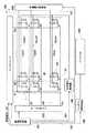
図1に示すように、本実施の形態に係る液晶表示装置100は、表示部を構成する液晶パネル200と、液晶パネル200を駆動するゲートドライバ102及びソースドライバ103と、ゲートドライバ102及びソースドライバ103を制御する駆動制御部101と、液晶パネル200の後述する対向電極Cntxの電位を制御する対向電圧制御部106と、液晶パネル200に表示用の光を供給するバックライト105と、バックライト105の輝度を制御するバックライト輝度制御部104と、図示されない転移電圧印加回路とを備えている。
【0041】
図2〜図4を併せて参照すると、液晶パネル200には、画素1がマトリクス状に形成され、このマトリクス状に形成された画素1の全体が表示画面を構成している。本実施の形態では、画素1がn行m列のマトリクスに形成されているものとし、画素1の行及び列に対応する構造体、信号等のうち、任意のものを表す場合にはそれらを示す符号にそれぞれx及びyの添え字を付して表す。この場合、x及びyは、それぞれ、1≦x≦n、1≦y≦mの値を取るものとする。
【0042】
図2に示すように、液晶パネル200は、互いに対向する対向基板201とTFT基板202との間に液晶層210が挟持され、両基板201,202の外側に位相差板203,204及び偏光板205,206がこの順にそれぞれ配設されて構成されている。
【0043】
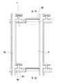
TFT基板202は、図4に示すように、断面視においては、大略、ガラス基板3の内面にゲート線Gx、絶縁層4、画素電極2及びソース線Sy、並びに配向膜(図示せず)等がこの順に積層されるように形成されるとともにゲート線Gx、ソース線Sy及び画素電極2に接続されるようにスイッチング素子としてのTFT(Thin Film Transistor:図4には示さず)が形成されて構成されている。そして、TFT基板202は、図1及び図3に示すように、平面視においては、n本のゲート線G1〜Gnとm本のソース線S1〜Smとが互いに直交するように形成され、このゲート線G1〜Gnとソース線S1〜Smとによって区画されるようにしてn行m列の画素1が形成されている。そして、各画素1毎に、各画素1に対応するゲート線Gx及びソース線Syの互いの交差点近傍にTFT10が形成されている。TFT10は、ソース、ドレイン、及びゲートが、それぞれ、ソース線Sy、画素電極2、及びゲート線Gxに接続されている。また、画素電極2の一部が、絶縁層4を介して(図4参照)前行の画素1に対応するゲート線Gx−1に重なるように形成され、この部分に蓄積容量(制御容量)30が形成されている。ここで、以下、「〜行の画素に対応するゲート線」を「〜段のゲート線」と略記する。また、「〜行又は〜列の画素に対応する〜」を「〜行又は〜列の〜」と略記する。そして、ゲート線G0〜Gn、ソース線S1〜Sm、及び対向電極Cnt1〜Cntnが、それぞれ、ゲートドライバ102、ソースドライバ103、及び対向電圧制御部106に接続されている。なお、ゲート線G0は第1行の画素電極2との間に後述する蓄積容量を形成するために設けられたものである。
【0044】
一方、対向基板201は、大略、ガラス基板(図示せず)の内面に対向電極Cnt1〜Cntn(図1参照)及び配向膜(図示せず)等が順に積層形成されて構成されている。図1では、対向電極Cnt1〜Cntnは、TFT基板202のマトリクス状の画素電極2の行に対応するように帯状にn本形成されているように描かれているが、実際には一方のガラス基板のほぼ全面に設けられている。
【0045】
次に、以上のように構成された液晶表示装置100の動作(駆動方法)を説明する。
【0046】
図1〜図4において、まず、液晶表示装置100が停止状態にあるときは、図2(a)に示すように、液晶層210は液晶分子210aがスプレイ配向をしている。そして、液晶表示装置100を始動すると、図示されない転移電圧印加回路により、液晶層210に所定の電圧(約25V)が所定時間印加され、液晶層210が図2(b),(c)に示すようなベンド配向に転移する。そして、液晶層210は、表示時における下限電圧下では図2(b)に示すように液晶分子210aが比較的湾曲した状態になり、表示時における上限電圧下では図2(c)に示すよう液晶分子210aが比較的立った状態になる。本実施の形態では、ノーマリホワイトモードを採用しているので、白表示及び黒表示時に、それぞれ、図2(b)及び図2(c)に示す状態になる。なお、ノーマリブラックモードの場合はこの逆になる。そして、このベンド配向の状態において、一定期間以上一定の電圧(通常、約2.1V)が印加されないと、スプレイ配向に逆転移する。
【0047】
そして、このように液晶層210がベンド配向に転移した後、駆動制御部101に制御されて、ゲートドライバ102及びソースドライバ103が以下のように動作する。また、その間、対向電圧制御部106が対向電極Cnt1〜Cntnの電位を所定値に制御し、バックライト輝度制御部104がバックライト105から液晶パネル200に供給する光の輝度(正確には光量)を所定値に制御する。
【0048】
すなわち、ゲートドライバ102が、ゲート線G1〜Gnを通じてゲート信号を出力して、画素1のTFT10をゲート線Gx毎に順次オンする。一方、ソースドライバ103は、映像信号110に基づいてソース信号を生成し、これをゲート信号にタイミングを合わせて、ソース線S1〜Smを通じて出力する。これにより、各画素1の画素電極2がソース信号に対応する電位に順次充電され、液晶層210が画素1毎に画素電極2の電位と対向電極Cntxの電位との差電圧(以下、液晶印加電圧という)に応じて変調され、バックライト105から供給される光に対する液晶パネル200の透過率が画素1毎にこの変調の程度に応じて変化する。そして、以上の動作が映像信号110のフレーム毎に繰り返されることにより、液晶パネル200の表示画面に映像信号110に応じた映像が表示される。なお、以下、画素1の画素電極2がソース信号の電位に対応する電位に充電されることを、画素電極2にソース信号が書き込まれると表現する。
【0049】
次に、図1〜図6を用いて、この動作を詳しく説明する。図5は図1の液晶表示装置におけるゲート信号、画素電極、及び対向電極の電位の変化を示す波形図、図6は逆転移防止電圧を説明するための図であって、(a)は画素における信号系統の等価回路を示す回路図、(b)はゲート信号における重畳電圧と画素電極に重畳される電圧との関係を示すタイミングチャート、(c)はノーマリホワイトモードにおける液晶印加電圧に対する液晶パネルの透過率の変化を示すグラフ、(d)はノーマリブラックモードにおける液晶印加電圧に対する液晶パネルの透過率の変化を示すグラフである。
【0050】
ゲートドライバ102は、図5に示すようなゲート信号Vg1〜Vgnを、それぞれ、ゲート線G1〜Gnに出力する。なお、ゲート線G0にはゲート信号Vgnと同じ信号が出力される。図5において、符号Tfは映像信号110におけるフレーム期間(フレーム周波数frの逆数)を示す。対向電極Cnt1〜Cntnの電位(以下、対向電圧という)Vcnt1〜Vcntnは、所定の一定値となるように設定されている。そして、図示されないソース信号は、ここでは、フレーム期間Tf毎に対向電圧Vcnt1〜Vcntnとの相対的な極性(ソース信号の電圧と対向電圧Vcnt1〜Vcntnとの差電圧、すなわち液晶印加電圧の極性:以下、単にソース信号の極性という)が反転させられている。以下、このソース信号が正及び負の極性になるフレーム期間を、それぞれ、正フレーム期間及び負フレーム期間という。
【0051】
ゲート信号Vg1〜Vgnは、書き込み期間TwにVgon、正フレームにおける重畳期間TarにVgar’、負フレームにおける重畳期間TarにVgar”、保持期間Thの重畳期間Tar以外の期間にVgoffの値を取る4値信号からなっている。書き込み期間Twは、ここでは、フレーム期間Tfを画素の行数nに等分した長さに設定されている。そして、各ゲート信号Vg1〜Vgnは、時間軸上におけるその書き込み期間Twの位置が、その対応する画素の行の順番が大きくなるにつれて、フレーム期間Tfの先頭から書き込み期間Twの幅づつ後方にずれていくように設定されている。そして、フレーム期間Tfからこの書き込み期間Twを除いた残りの期間が保持期間Thとなっている。そして、この保持期間Th内に所定長に渡って重畳期間Tarが設定されている。この重畳期間Tarは保持期間Th内であればその時間軸上の位置は任意であるが、ここでは、保持期間Thの時間軸上の略中央に位置するように設定されている。一方、ゲート信号Vg1〜Vgnの電圧値Vgon及びVgoffは、TFT10が、それぞれ、オン(導通)及びオフ(遮断)する値に設定されている。以下、このVgon及びVgoffを、それぞれ、ゲートオン電圧及びゲートオフ電圧と呼ぶ。また、ゲート信号Vg1〜Vgnの電圧値Var’及びVar”は、それぞれ、ゲートオフ電圧Vgoffより重畳電圧Varだけ高い値及びゲートオフ電圧Vgoffより重畳電圧Varだけ低い値に設定され、かつ共にTFT10がオンしないような値に設定されている。ここで、各電圧波形の具体例を示すと、例えば、画素電圧Vdx(ソース信号の電圧)の最大値及び最小値はそれぞれ5V及び−5V、対向電圧Vcntxは0V、ゲート信号Vgxのゲートオン電圧Vgon及びゲートオフ電圧Vgoffはそれぞれ10V及び−10V、重畳電圧Varは6Vに設定される。また、フレーム期間Tfは16.6msであり、書き込み期間Twは数十μsに設定される。また、重畳期間Tarは、後述する、画素電圧に重畳される電圧ΔVに応じて適宜設定される。
【0052】
このような設定により、ゲートドライバ102からゲート信号Vg1〜Vgnがゲート線G1〜Gnに出力されると、n行m列の画素1において、TFT10が、フレーム期間Tf毎に、列単位で行の順番に書き込み期間Twだけ順次オンする。そして、この各画素1におけるTFT10のオン期間(書き込み期間Tw)にタイミングを合わせて、ソースドライバ103から画素1の列毎にソース信号が出力され、そのソース信号がTFT10のオン期間に各画素1の画素電極2に書き込まれ、各画素1の画素電極2の電位(以下、画素電圧という)Vd1〜Vdnがそのソース信号の電位に略等しいものとなる。そして、各画素1において、書き込み期間Twが終了し、TFT10がオフするとその時点における画素電圧Vd1〜Vdnが保持される。なお、一般にソース信号、ひいては画素電圧Vdxは表示映像に依存した複雑な波形となるが、ここでは、簡略化のため逆転移が起こり得る一定電圧が印加されているものと仮定する。さらに、画素電圧Vdxには、TFT10のスイッチングに伴う当該段のゲート信号Vgxの変化によって、突き抜けと呼ばれる変化が生じるが、この説明は省略する。
【0053】
次に、本発明の特徴である逆転移防止電圧について説明するが、これは全ての画素について同様であるので、任意の1つの画素に着目してこれを説明する。第x行の画素1において、TFT10がオフした後、重畳期間Tfが到来すると、前段のゲート信号Vgx−1が重畳電圧Varだけ変化してVar’又はVar”になる(図6(b)にはVar’になる場合を示している)。すると、図6(b)に示すように、画素電圧Vdが、蓄積容量30を介してゲート信号Vgx−1における重畳電圧Varによる変化の影響を受けて変化する。この画素電圧Vdxの変化(以下、画素電極重畳電圧という)ΔVdは、以下のようになる。
【0054】
図6(a)に示すように、画素1の信号系統の等価回路においては、TFT10を介してソース線Syと接続された画素電極2が、対向電極Cntx及び前段のゲート線Gx−1と、それぞれ、液晶容量20及び蓄積容量30を介して接続されている。また、TFT10のドレイン及びこの延長部分たる画素電極2と当該段のゲート線Gxとの間には寄生容量Cgdが存在する。従って、液晶容量20及び蓄積容量30の容量を、それぞれ、Clc及びCstとすると、画素電極重畳電圧ΔVdは、
ΔVd=(Cst/(Clc+Cgd+Cst))Var・・・式(1)
となる。
【0055】
ここで、これらの数値の具体例を示すと、ΔVdは3V、Cstは0.4〜0.5pF、Clcは0.4〜0.5pF、Cgdは0.004〜0.005pF、Varは前述の通り6Vである。
【0056】
一方、逆転移電圧と表示時における電圧との関係は6(c)に示すようになっている。すなわち、ノーマリホワイトモードの場合、表示部の透過率は液晶印加電圧が増大するに連れて低下する。従って、白表示電圧Vwが表示時における下限電圧として設定され、黒表示電圧Vbが表示時における上限電圧として設定されている。この白表示電圧Vwから黒表示電圧Vbに至る電圧範囲R1が映像信号に応じて液晶印加電圧が取り得る電圧範囲である。そして、逆転移電圧、すなわち、一定期間以上これ以上の電圧が印加されないとOCBモードの液晶層210が逆転移を起こす閾値電圧Vtが、この表示電圧範囲R1内に存在する。従って、映像信号によって書き込まれた液晶印加電圧だけでは、それが逆転移電圧Vtを一定期間以上下回る場合には、液晶層210が逆転移することになる。しかし、本実施の形態では、画素電極重畳電圧ΔVdが、画素電圧Vdxひいては液晶印加電圧に重畳されるので、この画素電極重畳電圧ΔVdを|Vt−Vw|より大きく設定することにより、液晶印加電圧が取り得る電圧範囲は、逆転移電圧Vtを上回る電圧範囲R2へと移動し、それにより、液晶層210の逆転移を防止することができる。この画素電極重畳電圧ΔVdは1V以上とするのが望ましい。また、このとき、電圧範囲R2が黒表示電圧Vb以上の電圧範囲を含むことが望ましい。このようにすると、液晶印加電圧が黒表示電圧Vb以上となった場合には、画面に黒が表示されることになり、動画の切れが向上するからである。
【0057】
また、図6(c)から判るように、画素電極重畳電圧ΔVdを画素電圧Vdxに重畳すると液晶パネル200の透過率が低下することから、重畳期間Tarは短い程良い。本件発明者の実験によると、重畳期間Tarがフレーム期間Tfの10%以上であれば、好ましい映像表示が可能であることが確認されている。さらには、重畳期間Tarがフレーム期間Tfの50%以上であれば、動画ボケを防止する効果が得られる。
【0058】
なお、図5においてゲート信号Vgxの重畳電圧Varの極性を、ソース信号の極性に一致するよう設定したが、これは画素設計や電圧設定に応じて適宜設定することができ、必ずしも一致させる必要はない。
【0059】
また、本実施の形態では蓄積容量30を前段ゲート型としたが、蓄積容量を画素電極2と後段のゲート線Gx+1との間に形成する後段ゲート型としてもよい。
【0060】
また、本実施の形態においては、1つのゲート線単位で重畳電圧Varを印加しているが、隣接するあるいは離隔した複数のゲート線単位で重畳電圧Varを印加してもよい。つまり、1つのゲート線毎に異なるタイミングで重畳電圧Varを印加するのではなく、複数のゲート線毎に異なるタイミングで重畳電圧Varを印加してもよい。この場合、その印加される全ての重畳電圧Varの極性は、正の極性及び負の極性が略半数ずつであることが望ましい。これは、画素電圧の極性などによっては、対向電極への電圧カップリングの影響を取り除くために、重畳電圧Varの極性が全て同じではない方がよい場合が多いからである。
【0061】
また、本実施の形態ではノーマリホワイトモードとしたが、ノーマリブラックモードとすることもできる。この場合、図6(d)に示すように、白表示電圧Vwと黒表示電圧Vbとが入れ替わるが、その他の点はノーマリホワイトモードの場合と同様である。
【0062】
以上に説明したように、本実施の形態の液晶表示装置及びその駆動方法によれば、画素における保持期間中に画素電極重畳電圧ΔVを画素電圧に一時的に重畳することによって、OCB液晶の逆転移を防止することができる。なお、以降、この画素電極重畳電圧ΔVのような液晶層210の逆転移を防止するための電圧を逆転移防止電圧と呼ぶ。
実施の形態2
図7は本発明の実施の形態2に係る液晶表示装置におけるゲート信号、画素電圧、及び対向電圧の変化を示す波形図である。図7において図5と同一符号は同一又は相当する部分を示す。
【0063】
図7に示すように、本実施の形態は、実施の形態1とは異なり、ゲート信号Vg1〜Vgnに重畳電圧Varを重畳する重畳期間Tarを、時間軸上においてフレーム期間Tf内に対し一定位置に位置するよう設定したものである。その他の点は実施の形態1と同様である。重畳期間Tarは、ここでは、フレーム期間Tfの末尾に位置するよう設定されている。そして、書き込み期間Twは、フレーム期間Tfから重畳期間Tarを除いた期間を行数nに等分した長さに設定されている。このような構成とすると、全てのゲート信号G1〜Gnにおいて同時に重畳電圧Varが重畳されるので、下記変形例に示すように、バックライトをこの重畳電圧Varの重畳に合わせて暗くすることによりシャープな映像を得ることが可能になる。また、重畳期間Tarがフレーム期間Tfの末尾に位置するので、これを映像信号110のブランキング期間内に位置させることができ、それにより、映像の表示に支障を来たすことなく重畳電圧Varを重畳することができる。
【0064】
次に、本実施の形態の変形例を説明する。本変形例では、図1において、点線で示すように、駆動制御部101のクロック信号121がバックライト輝度制御部104に入力され、バックライト輝度制御部104が、このクロック信号121に基づいて、重畳期間Tarに渡ってバックライト105の輝度を下げあるいはバックライト105を消す。これにより、映像表示時と重畳期間Tarとのコントラスト比が上がり、よりシャープな映像表示が可能となる。その結果、液晶表示装置の表示上の課題の一つである、特にテレビなどの動画表示時におけるボケを低減することができる。
実施の形態3
図8は本発明の実施の形態3に係る液晶表示装置の構成を示す機能ブロック図、図9は図8の液晶表示装置におけるゲート信号、画素電圧、及び対向電圧の変化を示す波形図である。図8及び図9において、それぞれ、図1及び図5と同一符号は同一又は相当する部分を示す。
【0065】
図8に示すように、本実施の形態は、実施の形態1と異なり、制御駆動部101のクロック信号122が対向電圧制御部106に入力されている。その一方、画素電極とゲート線Gxとの間には蓄積容量が形成されておらず、従って、図1の蓄積容量形成のみを目的とした1段目のゲート線G0も設けられてはいない。これ以外の点は、実施の形態1と同様である。なお、必要に応じて蓄積容量を形成しても良い。
【0066】
次に、以上のように構成された液晶表示装置100の動作(駆動方法)を説明する。
【0067】
図8及び図9に示すように、対向電圧制御部106は、保持期間Th内の重畳期間Tarに渡って、対向電圧Vcntxに重畳電圧Varを重畳するようにこれを制御する。重畳期間Tarは、実施の形態2と同様に、フレーム期間Tfに対し時間軸上一定位置に位置するよう設定されており、具体的には、フレーム期間Tfの末尾に設定されている。重畳電圧Varの極性は、ソース信号の極性と反対である。つまり、正フレームでは負の極性の重畳電圧Varが重畳され、負フレームでは正の極性の重畳電圧Varが重畳される。その結果、この重畳電圧Varがそのまま液晶印加電圧に重畳され、実施の形態1における画素電極重畳電圧ΔVdと同様に作用する。従って、この重畳電圧(逆転移防止電圧)Varを実施の形態1における画素電極重畳電圧ΔVdと同様に設定することにより、液晶層210の逆転移を防止することができる。また、本実施の形態では、画素電極の電位を変化させないので、重畳期間Tarの前後において画素電極の電位の変動が少ない利点がある。
【0068】
また、本実施の形態の変形例として、図8において、点線で示すように、駆動制御部101のクロック信号121をバックライト輝度制御部104に入力し、バックライト輝度制御部104が、このクロック信号121に基づいて、重畳期間Tarに渡ってバックライト105の輝度を下げあるいはバックライト105を消すよう構成してもよい。それにより、映像表示時と重畳期間Tarとのコントラスト比が上がり、よりシャープな映像表示が可能となる。
【0069】
なお、重畳期間Tarを実施の形態1と同様に、保持期間Thに対し時間軸上一定位置に位置するよう設定してもよい。この場合、対向電極Cnt1〜Cntnを、TFT基板のマトリクス状の画素電極2の行に対応するように帯状にn本形成するとともに、図10に示すように、対向電圧制御部106に各対向電極Cnt1〜Cntnを互い並列に接続し、対向電圧制御部106によって各対向電極Cnt1〜Cntnの対向電圧Vcnt1〜Vcntnを個別に制御すればよい。
実施の形態4
図11は本発明の実施の形態4に係る液晶表示装置におけるゲート信号、画素電圧、及び対向電圧の変化を示す波形図である。図11において、図7及び図9と同一符号は同一又は相当する部分を示す。
【0070】
本実施の形態は実施の形態2と実施の形態3とを組み合わせたもので、液晶表示装置が、図8の構成において、図1に示す、第1行の画素の画素電極との間に蓄積容量30を形成するためのゲート線G0を有している。
【0071】
以上のように構成された液晶表示装置100では、図1、図8及び図11に示すように、ゲートドライバ102が、フレーム期間Tfの末尾に設定された重畳期間Tarに渡って第1の重畳電圧Var1をゲート信号Vg1〜Vgnに重畳し、対向電圧制御部106が、重畳期間Tarに渡って第2の重畳電圧Var2を対向電圧Vcnt1〜Vcntnに重畳する。これにより、液晶印加電圧は、第1の重畳電圧Var1による画素電極重畳電圧ΔVdと第2の重畳電圧Var2とが重畳されたものとなる。従って、この画素電極重畳電圧ΔVdと第2の重畳電圧Var2とを加えた電圧を図6(c),(d)の|Vt−Vw|より大きく設定することにより、液晶層210の逆転移を防止することができる。また、本実施の形態では、画素電極重畳電圧ΔVdと第2の重畳電圧Var2との2つの電圧を逆転移防止電圧として用いることができるので、逆転移防止電圧を実施の形態1及び2よりも高くすることができるため、重畳期間Tarを短縮することができる。
【0072】
また、実施の形態3と同様に、バックライト輝度制御部104が駆動制御部101からのクロック信号121に基づいて重畳期間Tar中にバックライト105を暗くするよう構成することにより、よりシャープな映像表示を得ることができる。
【0073】
また、重畳期間Tarを実施の形態1と同様に、保持期間Thに対し時間軸上一定位置に位置するよう設定してもよい。
実施の形態5
実施の形態1、2、及び4では、蓄積容量がゲート線上に形成された(以下、オンゲート型という)液晶表示装置に本発明を適用する場合を例示したが、本発明の実施の形態5は、蓄積容量が共通線上に形成された(以下、共通線型という)液晶表示装置に本発明を適用する場合を例示したものである。
【0074】
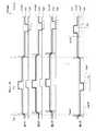
図12は本発明の実施の形態5に係る液晶表示装置の構成を示す機能ブロック図、図13は図12の液晶表示装置の液晶パネルの構成を示す平面図、図14は図13のXIV−XIV断面図である。図12、図13、及び図14において、それぞれ、図1、図3、及び図4と同一符号は同一又は相当する部分を示す。
【0075】
図12〜図14に示すように、本実施の形態では、実施の形態1と異なり、画素1の行毎に、ゲート線Gxに平行に共通線Comxが形成されている。この共通線Comxは、絶縁層4を介して画素電極2の下方に位置するように配設され、同一行に属する各画素電極2との間に蓄積容量(制御容量)30がそれぞれ形成されている。従って、図1の蓄積容量形成のみを目的としたゲート線G0は形成されいない。そして、各共通線Com1〜Comnの電位(以下、共通電圧という)Vcom1〜Vcomnを、共通電圧制御部107が制御駆動部101のクロック信号に基づいて制御している。これ以外の点は、実施の形態1と同様である。
【0076】
次に、以上のように構成された液晶表示装置の動作(駆動方法)を図12〜図15を参照して説明する。図15は図12の液晶表示装置におけるゲート信号、画素電圧、対向電圧、及び共通電圧の変化を示す波形図であり、図15において図5と同一符号は同一又は相当する部分を示す。また、図15において、共通電圧Vcomxは、重畳期間Tarを除き、対向電圧Vcntxと同じ一定電圧になるよう設定されており、図15では、この共通電圧Vcomxを重畳期間Tarにおいてのみ一点鎖線で示している。もちろん、重畳期間Tar以外における共通電圧Vcomxを対向電圧Vcntxと異なる一定電圧に設定しても構わない。
【0077】
図12〜図15において、共通電圧制御部107は、保持期間Th内の重畳期間Tarに渡って、共通電圧Vcomxに重畳電圧Varを重畳するようにこれを制御する。重畳期間Tarは、実施の形態1と同様に、時間軸において保持期間Thの略中央に位置に位置するよう設定されている。重畳電圧Varの極性は、ソース信号から画素電極に書き込まれた画素電圧Vdxの極性と同一である。これにより、重畳期間Tfが到来すると、共通電圧Vcomxが重畳電圧Varだけ変化し、この重畳電圧Varによる変化の影響を蓄積容量30を介して受けて、画素電圧Vdxが変化する。この画素電圧Vdxの変化、すなわち画素電極重畳電圧ΔVdは実施の形態1で述べた式(1)で与えられる。
【0078】
従って、この画素電極重畳電圧ΔVdを、図6(c),(d)の|Vt−Vw|より大きく設定することにより、液晶層210の逆転移を防止することができる。
【0079】
なお、本実施の形態においては、1つの共通線単位で重畳電圧Varを印加しているが、隣接するあるいは離隔した複数の共通線単位で重畳電圧Varを印加してもよい。
実施の形態6
図16は本発明の実施の形態6に係る液晶表示装置におけるゲート信号、画素電圧、対向電圧、及び共通電圧の変化を示す波形図である。図16において図15と同一符号は同一又は相当する部分を示す。また、図16において、共通電圧Vcomxは、重畳期間Tarを除き、対向電圧Vcntxと同じ一定電圧になるよう設定されており、図16では、この共通電圧Vcomxを重畳期間Tarにおいてのみ一点鎖線で示している。
【0080】
図16に示すように、本実施の形態は、実施の形態5とは異なり、共通電圧Vcom1〜Vcomnに重畳電圧Varを重畳する重畳期間Tarを、時間軸上においてフレーム期間Tf内に対し一定位置に位置するよう設定したものである。その他の点は実施の形態5と同様である。重畳期間Tarは、ここでは、フレーム期間Tfの末尾に位置するよう設定されている。そして、書き込み期間Twは、フレーム期間Tfから重畳期間Tarを除いた期間を行数nに等分した長さに設定されている。このような構成とすると、全ての共通電圧Vcom1〜Vcomnにおいて同時に重畳電圧Varが重畳されるので、下記変形例に示すように、バックライトをこの重畳電圧Varの重畳に合わせて暗くすることによりシャープな映像を得ることが可能になる。また、重畳期間Tarがフレーム期間Tfの末尾に位置するので、これを映像信号110のブランキング期間内に位置させることができ、それにより、映像の表示に支障を来たすことなく、重畳電圧Varを重畳することができる。
【0081】
次に、本実施の形態の変形例を説明する。本変形例では、図12において、点線で示すように、駆動制御部101のクロック信号121がバックライト輝度制御部104に入力され、バックライト輝度制御部104が、このクロック信号121に基づいて、重畳期間Tarに渡ってバックライト105の輝度を下げあるいはバックライト105を消す。これにより、映像表示時と重畳期間Tarとのコントラスト比が上がり、よりシャープな映像表示が可能となる。
実施の形態7
図17は本発明の実施の形態7に係る液晶表示装置におけるゲート信号、画素電圧、対向電圧、及び共通電圧の変化を示す波形図である。図17において、図9及び図16と同一符号は同一又は相当する部分を示す。また、図17において、共通電圧Vcomxは、重畳期間Tarを除き、対向電圧Vcntxと同じ一定電圧になるよう設定されており、図17では、この共通電圧Vcomxを重畳期間Tarにおいてのみ一点鎖線で示している。
【0082】
本実施の形態は実施の形態3と実施の形態6とを組み合わせたもので、対向電圧制御部106が、図12に点線で示すように、駆動制御101からクロック信号122を入力されている。
【0083】
以上のように構成された液晶表示装置100では、図12及び図17に示すように、共通電圧制御部107が、フレーム期間Tfの末尾に設定された重畳期間Tarに渡って第1の重畳電圧Var1を共通電圧Vcom1〜Vcomnに重畳し、対向電圧制御部106が、重畳期間Tarに渡って第2の重畳電圧Var2を対向電圧Vcnt1〜Vcntnに重畳する。これにより、液晶印加電圧は、第1の重畳電圧Var1による画素電極重畳電圧ΔVdと第2の重畳電圧Var2とが重畳されたものとなる。従って、この画素電極重畳電圧ΔVdと第2の重畳電圧Var2とを加えた電圧を図6(c),(d)の|Vt−Vw|より大きく設定することにより、液晶層210の逆転移を防止することができる。また、本実施の形態では、画素電極重畳電圧ΔVdと第2の重畳電圧Var2との2つの電圧を逆転移防止電圧として用いることができるので、逆転移防止電圧を実施の形態3及び6よりも高くすることができるため、重畳期間Tarを短縮することができる。
【0084】
また、実施の形態3と同様に、バックライト輝度制御部104が駆動制御部101からのクロック信号121に基づいて重畳期間Tar中にバックライト105を暗くするよう構成することにより、よりシャープな映像表示を得ることができる。
【0085】
また、重畳期間Tarを実施の形態5と同様に、保持期間Thに対し時間軸上一定位置に位置するよう設定してもよい。
実施の形態8
図18は本発明の実施の形態8に係る液晶表示装置の構成を示す機能ブロック図、図19は図18の液晶表示装置の液晶パネルの構成を示す平面図、図20は図19のXX−XX断面図である。図18〜図20において、図1〜図4、及び図12〜図14と同一符号は同一又は相当する部分を示す。
【0086】
本実施の形態は、実施の形態1と実施の形態5とを組み合わせたもので、実施の形態1の構成において、さらに、実施の形態5で述べたように、画素1の行毎に、ゲート線Gxに平行に共通線Comxが形成され、この共通線Comxと同一行に属する各画素電極2との間に蓄積容量がそれぞれ形成されている。本実施の形態では、画素電極2とゲート線Gxとの間に形成された蓄積容量を第1の蓄積容量31と呼び、画素電極2と共通線Comxとの間に形成された蓄積容量を第2の蓄積容量32と呼ぶ。
【0087】
次に、以上のように構成された液晶表示装置の動作(駆動方法)を図18〜図22を参照して説明する。図21は図18の液晶表示装置の画素における信号系統の等価回路を示す回路図、図22は図18の液晶表示装置におけるゲート信号、画素電圧、対向電圧、及び共通電圧の変化を示す波形図である。図21において図6(a)と同一符号は同一又は相当する部分を示す。また、図22において図5及び図15と同一符号は同一又は相当する部分を示す。さらに、図22において、共通電圧Vcomxは、重畳期間Tarを除き、対向電圧Vcntxと同じ一定電圧になるよう設定されており、図22では、この共通電圧Vcomxを重畳期間Tarにおいてのみ一点鎖線で示している。
【0088】
図18〜図22において、ゲートドライバ102は、保持期間Th内の重畳期間Tarに渡って、ゲート信号Vgx−1に第1の重畳電圧Var1を重畳し、共通電圧制御部107は、その重畳期間Tarに渡って、共通電圧Vcomxに第2の重畳電圧Var2を重畳するようにこれを制御する。重畳期間Tarは、実施の形態1と同様に、時間軸において保持期間Thの略中央に位置に位置するよう設定されている。第1、第2の重畳電圧Var1,Var2の極性は、共に、ソース信号から画素電極に書き込まれた画素電極Vdxの極性と同一である。これにより、重畳期間Tfが到来すると、ゲート信号Vgx−1及び共通電圧Vcomxが、それぞれ、第1の重畳電圧Var1及び第2の重畳電圧Var2だけ変化し、この第1の重畳電圧Var1及び第2の重畳電圧Var2による変化の影響を、それぞれ、第1の蓄積容量31及び第2の蓄積容量32を介して受けて、画素電圧Vdxが変化する。この画素電圧Vdxの変化たる画素電極重畳電圧(逆転移防止電圧)ΔVdは以下のようになる。
【0089】
図21に示すように、画素1の信号系統の等価回路においては、第1の蓄積容量31と第2の蓄積容量32とが互いに並列に接続されている。従って、第1の蓄積容量31及び第2の蓄積容量32の容量を、それぞれ、Cst1及びCst2とすると、画素電極重畳電圧ΔVdは、
ΔVd=(Cst1/Ct)Var1+(Cst2/Ct)Var2・・・式(2)
となる。
【0090】
ここで、Ct=Cgd+Clc+Cst1+Cst2であり、Cgd及びClcは、実施の形態1で説明したように、それぞれ、TFT10のゲート−ドレイン間の寄生容量及び液晶容量20の容量である。
【0091】
従って、この画素電極重畳電圧ΔVdを、図6(c),(d)の|Vt−Vw|より大きく設定することにより、液晶層210の逆転移を防止することができる。
【0092】
本実施の形態において、ゲート線Gxのみに重畳電圧を重畳した場合には実施の形態1と、共通電圧のみに重畳電圧を重畳した場合には実施の形態5と同じになる。本実施の形態では、第1の重畳電圧Var1と第2の重畳電圧Var2とが同じタイミングで同じ期間だけ重畳されている。このように第1の重畳電圧Var1と第2の重畳電圧Var2とが少なくとも部分的に重なり合っているときには、より高い電圧を画素電圧に重畳することができるので、ゲートドライバ102や共通電圧制御部107の耐圧が低い場合に逆転移を防止するのに有効である。また、それらの耐圧が充分に高い場合には、第1の重畳電圧Var1と第2の重畳電圧Var2とを離隔した期間に印加して、1フレーム期間Tf内に二度重畳電圧を重畳することでゲートドライバ102及び共通電圧制御部107の負荷を低減することができる。
【0093】
なお、本実施の形態においては、1つのゲート線及び共通線単位でそれぞれ第1、第2の重畳電圧Var1,Var2を印加しているが、隣接するあるいは離隔した複数のゲート線及び共通線単位でそれぞれ第1、第2の重畳電圧Var1,Var2重畳電圧Varを印加してもよい。
実施の形態9
図23は本発明の実施の形態9に係る液晶表示装置におけるゲート信号、画素電圧、対向電圧、及び共通電圧の変化を示す波形図である。図23において図22と同一符号は同一又は相当する部分を示す。また、図23において、共通電圧Vcomxは、重畳期間Tarを除き、対向電圧Vcntxと同じ一定電圧になるよう設定されており、図23では、この共通電圧Vcomxを重畳期間Tarにおいてのみ一点鎖線で示している。
【0094】
図23に示すように、本実施の形態は、実施の形態8とは異なり、ゲート信号Vg1〜Vgn及び共通電圧Vcom1〜Vcomnに、それぞれ、第1の重畳電圧Var1及び第2の重畳電圧Var2を重畳する重畳期間Tarを、時間軸上においてフレーム期間Tf内に対し一定位置に位置するよう設定したものである。その他の点は実施の形態8と同様である。重畳期間Tarは、ここでは、フレーム期間Tfの末尾に位置するよう設定されている。そして、書き込み期間Twは、フレーム期間Tfから重畳期間Tarを除いた期間を行数nに等分した長さに設定されている。このような構成とすると、全ての共通電圧Vcom1〜Vcomnにおいて同時に重畳電圧Varが重畳されるので、下記変形例に示すように、バックライトをこの重畳電圧Varの重畳に合わせて暗くすることによりシャープな映像を得ることが可能になる。また、重畳期間Tarがフレーム期間Tfの末尾に位置するので、これを映像信号110のブランキング期間内に位置させることができ、それにより、映像の表示に支障を来たすことなく重畳電圧Varを重畳することができる。
【0095】
次に、本実施の形態の変形例を説明する。本変形例では、図18において、点線で示すように、駆動制御部101のクロック信号121がバックライト輝度制御部104に入力され、バックライト輝度制御部104が、このクロック信号121に基づいて、重畳期間Tarに渡ってバックライト105の輝度を下げあるいはバックライト105を消す。これにより、映像表示時と重畳期間Tarとのコントラスト比が上がり、よりシャープな映像表示が可能となる。
実施の形態10
図24は本発明の実施の形態10に係る液晶表示装置におけるゲート信号、画素電圧、対向電圧、及び共通電圧の変化を示す波形図である。図24において、図9及び図23と同一符号は同一又は相当する部分を示す。また、図24において、共通電圧Vcomxは、重畳期間Tarを除き、対向電圧Vcntxと同じ一定電圧になるよう設定されており、図24では、この共通電圧Vcomxを重畳期間Tarにおいてのみ一点鎖線で示している。
【0096】
本実施の形態は実施の形態3と実施の形態8とを組み合わせたもので、対向電圧制御部106が、図18に点線で示すように、駆動制御101からクロック信号122を入力されている。
【0097】
以上のように構成された液晶表示装置100では、図18及び図24に示すように、ゲートドライバ102がフレーム期間Tfの末尾に設定された重畳期間Tarに渡って第1の重畳電圧Var1をゲート信号Vg1〜Vgnに重畳し、共通電圧制御部107がその重畳期間Tarに渡って第2の重畳電圧Var2を共通電圧Vcom1〜Vcomnに重畳し、かつ対向電圧制御部106がその重畳期間Tarに渡って第3の重畳電圧Var3を対向電圧Vcnt1〜Vcntnに重畳する。これにより、液晶印加電圧は、第1、第2の重畳電圧Var1,Var2による画素電極重畳電圧ΔVdと第3の重畳電圧Var3とが重畳されたものとなる。従って、この画素電極重畳電圧ΔVdと第3の重畳電圧Var3とを加えた電圧を図6(c),(d)の|Vt−Vw|より大きく設定することにより、液晶層210の逆転移を防止することができる。また、本実施の形態では、第1〜第3の重畳電圧Var1〜Var3の3つの重畳電圧を逆転移防止電圧に利用できるので、逆転移防止電圧をより高くすることができる。そのため、重畳期間Tarをより短縮することができる。
【0098】
また、実施の形態9と同様に、バックライト輝度制御部104が駆動制御部101からのクロック信号121に基づいて重畳期間Tar中にバックライト105を暗くするよう構成することにより、よりシャープな映像表示を得ることができる。
【0099】
また、重畳期間Tarを、実施の形態8と同様に、保持期間Thに対し時間軸上一定位置に位置するよう設定してもよい。
【0100】
なお、前記実施の形態2〜10において、実施の形態1で述べたように、重畳期間がフレーム期間Tfの10%以上であれば、好ましい映像表示が可能であり、50%以上であれば、動画ボケを防止する効果が得られる。また、ノーマリブラックモードとすることもできる。
【0101】
また、前記実施の形態2、4〜10において、ゲート信号Vgx及び共通電圧Vcomxの重畳電圧Var,Var1,Var2の極性は、ソース信号の極性に必ずしも一致させる必要はない。また、その印加される全ての重畳電圧Var,Var1,Var2の極性は、正の極性及び負の極性が略半数ずつであることが望ましい。また、蓄積容量を画素電極2と後段のゲート線Gx+1との間に形成する後段ゲート型としてもよい。
【0102】
また、前記実施の形態3、4、7、9、10において、対向電圧Vcntxにおける重畳期間Tarを、フレーム期間Tf内の時間軸上の一定位置に設定する場合には、各対向電圧Vcntxを独立して制御する必要がないので、画素1の行毎に対向電極Cntxを設ける必要はなく、対向基板201の略全面に渡って1つの対向電極を設けてもよい。これは、実施の形態1、2、5、6、8においても同様であることは言うまでもない。
【0103】
また、上記実施の形態1〜10では、逆転移防止電圧が1フレーム期間毎に重畳されるが、例えば、映像信号のフレーム周波数が高いような場合には、逆転移防止電圧が複数フレーム期間毎に1回重畳されるようにしてもよい。
【0104】
また、上記実施の形態1〜10では、スイッチング素子10としてTFTを用いたがこれに代えて、ダイオードを用いてもよい。
【0105】
【発明の効果】
本発明は以上に説明したような形態で実施され、非表示時とは異なる配向状態に転移させて表示を行う液晶モードの液晶表示装置において、逆転移の発生を抑制しつつ映像を表示することができるという効果を奏する。
【図面の簡単な説明】
【図1】本発明の実施の形態1に係る液晶表示装置の構成を示す機能ブロック図である。
【図2】図1の液晶表示装置の液晶パネルの構成及び液晶層の配向状態を示す断面図であって、(a)は無電圧下における配向状態を示す図、(b)は表示時の下限電圧下における配向状態を示す図、(c)は表示時の上限電圧下における配向状態を示す図である。
【図3】図1の液晶表示装置の液晶パネルの構成を示す平面図である。
【図4】図3のIV−IV断面図である。
【図5】図1の液晶表示装置におけるゲート信号、画素電極、及び対向電極の電位の変化を示す波形図である。
【図6】逆転移防止電圧を説明するための図であって、(a)は画素における信号系統の等価回路を示す回路図、(b)はゲート信号における重畳電圧と画素電極に重畳される電圧との関係を示すタイミングチャート、(c)はノーマリホワイトモードにおける液晶印加電圧に対する液晶パネルの透過率の変化を示すグラフ、(d)はノーマリブラックモードにおける液晶印加電圧に対する液晶パネルの透過率の変化を示すグラフである。
【図7】本発明の実施の形態2に係る液晶表示装置におけるゲート信号、画素電圧、及び対向電圧の変化を示す波形図である。
【図8】本発明の実施の形態3に係る液晶表示装置の構成を示す機能ブロック図である。
【図9】図8の液晶表示装置におけるゲート信号、画素電圧、及び対向電圧の変化を示す波形図である。
【図10】本発明の実施の形態3の変形例に係る液晶表示装置の構成を示す機能ブロック図である。
【図11】本発明の実施の形態4に係る液晶表示装置におけるゲート信号、画素電圧、及び対向電圧の変化を示す波形図である。
【図12】本発明の実施の形態5に係る液晶表示装置の構成を示す機能ブロック図である。
【図13】図12の液晶表示装置の液晶パネルの構成を示す平面図である。
【図14】図13のXIV−XIV断面図である。
【図15】図12の液晶表示装置におけるゲート信号、画素電圧、対向電圧、及び共通電圧の変化を示す波形図である。
【図16】本発明の実施の形態6に係る液晶表示装置におけるゲート信号、画素電圧、対向電圧、及び共通電圧の変化を示す波形図である。
【図17】本発明の実施の形態7に係る液晶表示装置におけるゲート信号、画素電圧、対向電圧、及び共通電圧の変化を示す波形図である。
【図18】本発明の実施の形態8に係る液晶表示装置の構成を示す機能ブロック図である。
【図19】図18の液晶表示装置の液晶パネルの構成を示す平面図である。
【図20】図19のXX−XX断面図である。
【図21】図18の液晶表示装置の画素における信号系統の等価回路を示す回路図である。
【図22】図18の液晶表示装置におけるゲート信号、画素電圧、対向電圧、及び共通電圧の変化を示す波形図である。
【図23】本発明の実施の形態9に係る液晶表示装置におけるゲート信号、画素電圧、対向電圧、及び共通電圧の変化を示す波形図である。
【図24】本発明の実施の形態10に係る液晶表示装置におけるゲート信号、画素電圧、対向電圧、及び共通電圧の変化を示す波形図である。
【符号の説明】
1 画素
2 画素電極
3 ガラス基板
4 絶縁層
10 TFT
20 液晶容量
30 蓄積容量
31 第1の蓄積容量
101 駆動制御部
32 第2の蓄積容量
100 液晶表示装置
101 駆動制御部
102 ゲートドライバ
103 ソースドライバ
104 バックライト輝度制御部
105 バックライト
106 対向電圧制御部
107 共通電圧制御部
110 映像信号
121,122 クロック信号
200 液晶パネル
201 対向基板
202 TFT基板
203,204 位相差板
205,206 偏光板
210 液晶層
210a 液晶分子
Cgd ゲート−ドレイン間寄生容量
Clc 液晶容量の容量
Cnt1〜Cntn 対向電極
Com1〜Comn 共通線
Cst,Cst1,Cst2 蓄積容量の容量
G0〜Gn ゲート線
R1,R2 電圧範囲
S1〜Sm ソース線
Tar 重畳期間
Tar1〜Tar3 第1〜第3の重畳期間
Tf フレーム期間
Th 保持期間
Tw 書き込み期間
Var 重畳電圧
Var1〜Var3 第1〜第3の重畳電圧
Vb 黒表示電圧
Vcnt1〜Vcntn 対向電圧
Vcom1〜Vcomn 共通電圧
Vd1〜Vdn 画素電圧
Vg1〜Vgn ゲート信号
Vgon ゲートオン電圧
Vgoff ゲートオフ電圧
Vt 逆転移電圧
Vw 白表示電圧
ΔVd 画素電圧に重畳される電圧[0001]
TECHNICAL FIELD OF THE INVENTION
The present invention relates to a method for driving a liquid crystal display device and a liquid crystal display device, and in particular, differs from a non-display state.BentoDisplay by shifting to orientation stateOCBThe present invention relates to a liquid crystal display device using a liquid crystal mode and a driving method thereof.
[0002]
[Prior art]
Liquid crystal display devices have been used in displays of desktop personal computers and mobile phones, starting with notebook personal computers. Further, in recent years, in addition to these, application to a liquid crystal TV has started. However, the TN (Twisted Nematic) liquid crystal mode, which is currently widely used, has many problems in terms of viewing angle, response speed, and the like, and particularly in moving image display performance for TV applications.
[0003]
Therefore, in recent years, studies on an OCB (optically self-compensated birefringence) liquid crystal mode as a liquid crystal mode replacing the TN liquid crystal mode have been actively conducted. The OCB liquid crystal mode has a wider viewing angle and a faster response speed than the TN liquid crystal mode, and thus can be said to be a liquid crystal mode more suitable for displaying moving images. However, the OCB liquid crystal mode requires its own drive before displaying an image. In other words, in the OCB liquid crystal mode, there are two alignment states (see FIG. 2A): a bend alignment in which an image can be displayed (see FIGS. 2B and 2C) and a splay alignment in which an image cannot be displayed. In order to shift the OCB liquid crystal in the splay alignment to the bend alignment (hereinafter, this phenomenon is called transition), a special drive such as applying a high voltage (for example, about 25 V) to the liquid crystal layer for a certain period of time is required. . However, since the driving relating to the transition is not directly related to the present invention, a detailed description is omitted.
[0004]
[Problems to be solved by the invention]
However, even if the OCB liquid crystal transitions from the splay alignment to the bend alignment, the bend alignment may be maintained if a voltage (for example, about 2.1 V) higher than a predetermined level is not applied to the liquid crystal layer for a certain period of time. There has been a problem that a phenomenon of returning to the splay alignment without being performed (hereinafter, this phenomenon is called a reverse transition) occurs.
[0005]
At this point, the OCB liquid crystal mode is the only liquid crystal mode in which display is performed by transiting to a different alignment state from the non-display state (when no voltage is applied). Therefore, such a problem occurs only in the OCB liquid crystal mode. If, in the future, a liquid crystal mode for performing display by transferring to an alignment state different from the non-display state as in the OCB liquid crystal mode is developed, similar problems occur in such a liquid crystal mode.
[0006]
The present invention relates to a driving method of a liquid crystal display device and a liquid crystal display device capable of displaying an image while suppressing the occurrence of a reverse transition when employing a liquid crystal mode in which display is performed by transitioning to an orientation state different from a non-display state. It is intended to provide.
[0007]
[Means for Solving the Problems]
In order to solve the above-mentioned problems, a driving method of a liquid crystal display device and a liquid crystal display deviceBendOrientation state and non-displaySprayHas orientation stateOCBA liquid crystal layer, and a plurality of pixels, wherein a video signal is sequentially written to the plurality of pixels for each frame, and a voltage corresponding to the video signal is held in each pixel, and the voltage is set according to the held voltage.OCBIn a liquid crystal display device in which an image is displayed by controlling the degree of modulation of the liquid crystal layer,blackA voltage corresponding to the video signal smaller than a threshold voltage existing between a display voltage and a white display voltage for a certain period or more,OCBDue to the application to the liquid crystal layer.BendFrom the orientation state for the non-displaySprayIn order to prevent the reverse transition from shifting to the alignment state, during the holding period of the voltage corresponding to the video signal, the reverse transition equal to or more than the absolute value of the difference voltage between the threshold voltage and the lower limit voltage of the voltage corresponding to the video signal. The prevention voltage is temporarily superimposed on the voltage corresponding to the video signal.The OCB liquid crystal layer is sandwiched between a pair of substrates facing each other, a pixel electrode corresponding to the plurality of pixels is formed on one inner surface of the pair of substrates, and the other inner surface of the pair of substrates is formed. A switching element is provided for each of the plurality of pixels, and the switching elements are sequentially turned on and off through a gate line, so that each pixel is turned on at the time of the on-state. The video signal is written and a voltage corresponding to the written video signal when the video signal is turned off is held by a liquid crystal capacitance between the pixel electrode and the counter electrode sandwiching the OCB liquid crystal layer, and the voltage is applied to the gate line. A predetermined voltage is superimposed on the pixel electrode or between the gate line and a conductor connected to the pixel electrode separately from the liquid crystal capacitor. The reverse transition prevention voltage is superimposed on a voltage corresponding to the video signal via the formed control capacitor.(Claim1, 11). With this configuration, it is different from non-displayBendIn the orientation state, an image can be displayed while suppressing the occurrence of reverse transition. Also, by temporarily superimposing a reverse transition prevention voltage equal to or more than the absolute value of a difference voltage between the threshold voltage and the lower limit voltage of the voltage corresponding to the video signal on the voltage corresponding to the video signal, it is ensured.OCBLiquid crystal layerofReverse metastasis can be prevented.Further, with this configuration, the reverse transition prevention voltage can be superimposed on the voltage corresponding to the video signal with a simple configuration, and more specifically, the reverse transition prevention voltage can be superimposed using the gate line.
[0011]
Further, the predetermined voltages superimposed on the respective gate lines may include voltages having opposite polarities.2,12). With this configuration, it is possible to reduce the influence of voltage coupling to the counter electrode due to the polarity of the pixel voltage and the like.
[0012]
When the reverse transition prevention voltage is ΔVd, the capacitance of the liquid crystal capacitance is Clc, the capacitance of the control capacitance is Cst, and the parasitic capacitance of the switching element is Cgd, a predetermined voltage superimposed on the gate line is Clc + Cst + Cgd. ) / Cst × ΔVdNo.With this configuration, a desired reverse transition prevention voltage can be appropriately set.
[0013]
Further, the plurality of pixels are formed in a matrix, the gate line is formed for each row or column of the plurality of pixels, and the source line is formed for each column or row of the plurality of pixels. Is connected to the corresponding source line via each switching element, and the control terminal of each switching element is connected to the corresponding gate line, and the switching element of each pixel is sequentially turned on for each gate line. The video signal may be supplied to each pixel through the source line at the same time asNo.
[0014]
Further, the predetermined voltage may be superimposed on each gate line.No.
[0015]
Further, the predetermined voltage may be superimposed on a plurality of gate line units.No.With this configuration, the configuration of the gate line driver circuit can be simplified.
[0016]
Further, the plurality of gate lines may correspond to rows or columns of continuous pixels.No.
[0017]
Further, the switching element may be a thin film transistor.No.
[0019]
A method for driving a liquid crystal display device and a liquid crystal display device according to the present invention include an OCB liquid crystal layer having a bend alignment state for display and a splay alignment state for non-display, and a plurality of pixels. A liquid crystal display in which a video signal is sequentially written for each frame, a voltage corresponding to the video signal is held in each pixel, and a modulation degree of the OCB liquid crystal layer is controlled according to the held voltage to display a video. In the device, the display bend caused by applying a voltage corresponding to the video signal smaller than a threshold voltage existing between a black display voltage and a white display voltage to the OCB liquid crystal layer for a predetermined period or more. In order to prevent a reverse transition from shifting from the alignment state to the non-display splay alignment state, the threshold voltage and the voltage corresponding to the video signal are reduced during the holding period of the voltage corresponding to the video signal. Voltage absolute value than the reverse transition prevention voltage are temporarily added to the voltage corresponding to the video signal of the differential voltage between,Between a pair of substrates facing each otherOCBA liquid crystal layer is sandwiched, a pixel electrode corresponding to the plurality of pixels is formed on one inner surface of the pair of substrates, and a counter electrode is formed on the other inner surface of the pair of substrates. A switching element is provided in each of the plurality of pixels, and the switching element is sequentially turned on and off through a gate line, whereby the video signal is written in each pixel when the pixel is turned on and the written signal is written in the pixel when the pixel is turned off. The voltage corresponding to the video signal isOCBIt is held by a liquid crystal capacitance between the pixel electrode and the counter electrode sandwiching a liquid crystal layer, and further includes a common line, and a predetermined voltage is superimposed on the common line, so that the liquid crystal capacitance is separated from the liquid crystal capacitance. The reverse transition prevention voltage is superimposed on a voltage corresponding to the video signal via a control capacitor formed between a pixel electrode or a conductor connected to the pixel electrode and the common line.Is(Claim3, 13). Even with such a configuration, the reverse transition prevention voltage can be superimposed with a simple configuration.
[0020]
Assuming that the reverse transition prevention voltage is ΔVd, the capacitance of the liquid crystal capacitance is Clc, the capacitance of the control capacitance is Cst, and the parasitic capacitance of the switching element is Cgd, the predetermined voltage superimposed on the common line is ( Clc + Cst + Cgd) / Cst × ΔVdYou.With this configuration, a desired reverse transition prevention voltage can be appropriately set.
[0021]
Further, the common line may be formed for each row or column of the pixel, and the predetermined voltage may be superimposed on each common line unit.No.
[0022]
Further, the common line may be formed for each row or column of the pixel, and the predetermined voltage may be superimposed on a plurality of common line units.No.With this configuration, the configuration of the circuit for driving the common line can be simplified.
[0023]
Further, the plurality of common lines may correspond to rows or columns of continuous pixels.No.
[0024]
A common line, wherein another control capacitor is formed between the common line and the pixel electrode or a conductor connected to the pixel electrode, and another predetermined voltage is superimposed on the common line. Accordingly, another reverse transition prevention voltage may be further superimposed on the voltage corresponding to the video signal via the other control capacitor.4, 14). With this configuration, when the two reverse transition prevention voltages at least partially overlap, a higher voltage can be superimposed on the voltage corresponding to the video signal, so that the gate line driving circuit and the common line driving circuit , The reverse transition can be effectively prevented when the breakdown voltage is low.
[0025]
Further, at least one of the reverse transition prevention voltage and the other reverse transition prevention voltage may be superimposed.No.
[0026]
Further, both the reverse transition prevention voltage and the other reverse transition prevention voltage may be superimposed.No.
[0027]
When the reverse transition prevention voltage is ΔVd1, the other reverse transition prevention voltage is ΔVd2, the capacitance of the control capacitor is Cst1, and the capacitance of the other control capacitor is Cst2, the voltage is superimposed on a voltage corresponding to the video signal. The total reverse transition prevention voltage ΔVd is
ΔVd = ΔVd1 + ΔVd2
Where the predetermined voltage superimposed on the gate line is
(Clc + Cst1 + Cgd) / Cst1 × ΔVd1, and another predetermined voltage superimposed on the common line is:
(Clc + Cst2 + Cgd) / Cst2 × ΔVd2You.With this configuration, the two reverse transition prevention voltages can be appropriately set to desired values.
[0028]
A method for driving a liquid crystal display device and a liquid crystal display device according to the present invention include an OCB liquid crystal layer having a bend alignment state for display and a splay alignment state for non-display, and a plurality of pixels. A liquid crystal display in which a video signal is sequentially written for each frame, a voltage corresponding to the video signal is held in each pixel, and a modulation degree of the OCB liquid crystal layer is controlled according to the held voltage to display a video. In the device, the display bend caused by applying a voltage corresponding to the video signal smaller than a threshold voltage existing between a black display voltage and a white display voltage to the OCB liquid crystal layer for a predetermined period or more. In order to prevent a reverse transition from shifting from the alignment state to the non-display splay alignment state, the threshold voltage and the voltage corresponding to the video signal are reduced during the holding period of the voltage corresponding to the video signal. Voltage absolute value than the reverse transition prevention voltage are temporarily added to the voltage corresponding to the video signal of the differential voltage between,Between a pair of substrates facing each otherOCBA liquid crystal layer is sandwiched between the inner surfaces of one of the pair of substrates.Provided with a switching elementA pixel electrode corresponding to the plurality of pixels is formed, and the image display portion includes a counter electrode formed on the other inner surface of the pair of substrates, and the pixel electrode faces at least the pixel electrode sandwiching the liquid crystal layer. Depending on the liquid crystal capacitance between the electrodes, The switching elements are sequentially turned on through the gate lines to write data in each pixel.The voltage corresponding to the video signal,When the switching element is offIt is held and superimposes the reverse transition prevention voltage on the voltage corresponding to the video signal via the liquid crystal capacitor by temporarily changing the potential of the counter electrode.Is the thing(Claim5, 15). With this configuration, the reverse transition prevention voltage can be superimposed with a simple configuration.
[0029]
Further, the counter electrode may be formed for each predetermined group of the plurality of pixels.No.With this configuration, by controlling the potential of the counter electrode for each predetermined group of pixels, a different reverse transition prevention voltage can be set for each group.
[0030]
Further, the reverse transition prevention voltage may be superimposed over a superimposition period located at a fixed position on a time axis in a frame period of the video signal.6, 16). With this configuration, the reverse transition prevention voltage can be simultaneously superimposed on all the pixels. Therefore, for example, a sharp image display can be obtained by darkening the display light in accordance with the superimposition period.
[0031]
Further, the liquid crystal display device isOCBA lighting device that supplies display light whose transmittance is changed in accordance with the degree of modulation of the liquid crystal layer, wherein the lighting device reduces a supply amount of display light in accordance with the superimposition period. (Claims7, 17). With this configuration, the contrast ratio between the image display and the superimposition period is improved, so that a sharp image display can be obtained.
[0032]
Further, the superimposition period may be located within a blanking period of the video signal.8, 18). With this configuration, the reverse transition prevention voltage can be superimposed without disturbing the image display.
[0033]
Further, the display of the image is set to a normally white mode, and a possible voltage range of a voltage applied to the liquid crystal layer during the superposition of the reverse transition prevention voltage includes a voltage range equal to or more than a black display voltage. MoyoNo.With such a configuration, when the voltage applied to the liquid crystal layer becomes equal to or higher than the black display voltage, the break of the moving image is improved.
[0034]
Further, the display of the image is set to a normally black mode, and a possible voltage range of a voltage applied to the liquid crystal layer during the superposition of the reverse transition prevention voltage includes a voltage range equal to or more than a white display voltage. MoyoNo.Even with such a configuration, when the voltage applied to the liquid crystal layer becomes equal to or higher than the white display voltage, the break of the moving image is improved.
[0036]
Further, a period during which the reverse transition prevention voltage is superimposed may be 10% or more of a frame period of the video signal.9, 19). With this configuration, a preferable image display can be obtained.
[0037]
Further, a period during which the reverse transition prevention voltage is superimposed may be 50% or more of a frame period of the video signal.10, 20). With this configuration, moving image blur can be prevented.
[0039]
BEST MODE FOR CARRYING OUT THE INVENTION
Hereinafter, embodiments of the present invention will be described with reference to the drawings.
FIG. 1 is a functional block diagram showing a configuration of a liquid crystal display device according to
[0040]
As shown in FIG. 1, a liquid
[0041]
2 to 4, the
[0042]
As shown in FIG. 2, the
[0043]
As shown in FIG. 4, the
[0044]
On the other hand, the opposing
[0045]
Next, the operation (driving method) of the liquid
[0046]
1 to 4, first, when the liquid
[0047]
Then, after the
[0048]
That is, the
[0049]
Next, this operation will be described in detail with reference to FIGS. FIG. 5 is a waveform diagram showing changes in potentials of a gate signal, a pixel electrode, and a counter electrode in the liquid crystal display device of FIG. 1, and FIG. 6 is a diagram for explaining a reverse transition prevention voltage. Circuit diagram showing an equivalent circuit of a signal system in (a), (b) is a timing chart showing a relationship between a superimposed voltage in a gate signal and a voltage superimposed on a pixel electrode, and (c) is a liquid crystal with respect to a liquid crystal applied voltage in a normally white mode. FIG. 4D is a graph showing a change in transmittance of the panel, and FIG. 6D is a graph showing a change in transmittance of the liquid crystal panel with respect to a voltage applied to the liquid crystal in a normally black mode.
[0050]
The
[0051]
The gate signals Vg1 to Vgn take the values of Vgon during the writing period Tw, Vgar ′ during the superimposing period Tar in the positive frame, Vgar ”during the superimposing period Tar in the negative frame, and Vgoff during periods other than the superimposing period Tar of the holding period Th. In this case, the writing period Tw is set to a length obtained by equally dividing the frame period Tf by the number n of rows of pixels, and each of the gate signals Vg1 to Vgn on the time axis. The position of the writing period Tw is set so as to shift from the beginning of the frame period Tf to the rear by the width of the writing period Tw as the order of the row of the corresponding pixel increases. The remaining period excluding the writing period Tw is the holding period Th. The superimposition period Tar is set over the fixed length, and the position of the superimposition period Tar on the time axis is arbitrary within the holding period Th, but here, the superimposition period Tar is approximately on the time axis. On the other hand, the voltage values Vgon and Vgoff of the gate signals Vg1 to Vgn are set to values at which the
[0052]
With such a setting, when the gate signals Vg1 to Vgn are output from the
[0053]
Next, the reverse transition prevention voltage, which is a feature of the present invention, will be described. Since this is the same for all pixels, this will be described focusing on any one pixel. In the
[0054]
As shown in FIG. 6A, in the equivalent circuit of the signal system of the
ΔVd = (Cst / (Clc + Cgd + Cst)) Var (1)
It becomes.
[0055]
Here, as specific examples of these numerical values, ΔVd is 3 V, Cst is 0.4 to 0.5 pF, Clc is 0.4 to 0.5 pF, Cgd is 0.004 to 0.005 pF, and Var is as described above. It is 6V as shown in FIG.
[0056]
On the other hand, the relationship between the reverse transition voltage and the voltage at the time of display is as shown in FIG. That is, in the case of the normally white mode, the transmittance of the display unit decreases as the voltage applied to the liquid crystal increases. Therefore, the white display voltage Vw is set as the lower limit voltage during display, and the black display voltage Vb is set as the upper limit voltage during display. The voltage range R1 from the white display voltage Vw to the black display voltage Vb is a voltage range that the liquid crystal applied voltage can take according to the video signal. The reverse transition voltage, that is, the threshold voltage Vt at which the OCB mode
[0057]
Further, as can be seen from FIG. 6C, when the pixel electrode superimposed voltage ΔVd is superimposed on the pixel voltage Vdx, the transmittance of the
[0058]
In FIG. 5, the polarity of the superimposed voltage Var of the gate signal Vgx is set to match the polarity of the source signal. However, this can be set as appropriate according to the pixel design and the voltage setting. Absent.
[0059]
In the present embodiment, the
[0060]
Further, in the present embodiment, the superimposed voltage Var is applied in units of one gate line, but the superimposed voltage Var may be applied in units of a plurality of adjacent or separated gate lines. That is, instead of applying the superimposed voltage Var at different timings for one gate line, the superimposed voltage Var may be applied at different timings for a plurality of gate lines. In this case, it is desirable that the polarity of all the applied superimposed voltages Var is approximately half each of the positive polarity and the negative polarity. This is because, depending on the polarity of the pixel voltage and the like, it is often preferable that the polarities of the superimposed voltages Var are not all the same in order to remove the influence of voltage coupling to the counter electrode.
[0061]
In the present embodiment, the normally white mode is used, but the normally black mode may be used. In this case, as shown in FIG. 6D, the white display voltage Vw and the black display voltage Vb are switched, but the other points are the same as those in the normally white mode.
[0062]
As described above, according to the liquid crystal display device of the present embodiment and the method of driving the same, the OCB liquid crystal is inverted by temporarily superimposing the pixel electrode superimposed voltage ΔV on the pixel voltage during the holding period in the pixel. Transfer can be prevented. Hereinafter, a voltage for preventing reverse transition of the
FIG. 7 is a waveform chart showing changes in a gate signal, a pixel voltage, and a counter voltage in the liquid crystal display device according to
[0063]
As shown in FIG. 7, the present embodiment is different from the first embodiment in that the superimposition period Tar in which the superimposition voltage Var is superimposed on the gate signals Vg1 to Vgn is set at a certain position on the time axis with respect to the frame period Tf. It is set to be located at. Other points are the same as the first embodiment. Here, the superimposition period Tar is set to be located at the end of the frame period Tf. Then, the writing period Tw is set to a length obtained by equally dividing the period excluding the superimposition period Tar from the frame period Tf into the number n of rows. With such a configuration, the superimposed voltage Var is simultaneously superimposed on all the gate signals G1 to Gn. Therefore, as shown in the following modified example, the backlight is darkened in accordance with the superimposition of the superimposed voltage Var to sharpen the sharpness. It is possible to obtain a proper image. In addition, since the superimposition period Tar is located at the end of the frame period Tf, it can be positioned within the blanking period of the video signal 110, so that the superposition voltage Var can be superimposed without disturbing the display of the video. can do.
[0064]
Next, a modified example of the present embodiment will be described. In this modification, as shown by a dotted line in FIG. 1, a
FIG. 8 is a functional block diagram showing a configuration of a liquid crystal display device according to
[0065]
As shown in FIG. 8, the present embodiment differs from the first embodiment in that a
[0066]
Next, the operation (driving method) of the liquid
[0067]
As shown in FIGS. 8 and 9, the common
[0068]
As a modified example of the present embodiment, as shown by a dotted line in FIG. 8, a
[0069]
Note that, as in the first embodiment, the superimposition period Tar may be set to be located at a fixed position on the time axis with respect to the holding period Th. In this case, n counter electrodes Cnt1 to Cntn are formed in a strip shape so as to correspond to the rows of the
Embodiment 4
FIG. 11 is a waveform diagram showing changes in a gate signal, a pixel voltage, and a counter voltage in the liquid crystal display device according to Embodiment 4 of the present invention. 11, the same reference numerals as those in FIGS. 7 and 9 indicate the same or corresponding parts.
[0070]
This embodiment is a combination of the second embodiment and the third embodiment. In the liquid crystal display device shown in FIG. 8, the liquid crystal display device has the structure shown in FIG. It has a gate line G0 for forming the
[0071]
In the liquid
[0072]
Further, similar to the third embodiment, the backlight
[0073]
Further, similarly to the first embodiment, the superimposition period Tar may be set to be located at a fixed position on the time axis with respect to the holding period Th.
In the first, second, and fourth embodiments, the case where the present invention is applied to a liquid crystal display device in which a storage capacitor is formed on a gate line (hereinafter, referred to as an on-gate type) has been described. This is an example in which the present invention is applied to a liquid crystal display device in which storage capacitors are formed on a common line (hereinafter, referred to as a common line type).
[0074]
FIG. 12 is a functional block diagram showing a configuration of a liquid crystal display device according to
[0075]
As shown in FIGS. 12 to 14, in the present embodiment, unlike
[0076]
Next, the operation (driving method) of the liquid crystal display device configured as described above will be described with reference to FIGS. FIG. 15 is a waveform diagram showing changes in a gate signal, a pixel voltage, a counter voltage, and a common voltage in the liquid crystal display device in FIG. 12, and the same reference numerals in FIG. 15 as those in FIG. 5 indicate the same or corresponding parts. Further, in FIG. 15, the common voltage Vcomx is set to be the same constant voltage as the counter voltage Vcntx except for the superimposition period Tar. In FIG. 15, the common voltage Vcomx is indicated by a dashed line only in the superimposition period Tar. ing. Of course, the common voltage Vcomx other than the superimposition period Tar may be set to a constant voltage different from the common voltage Vcntx.
[0077]
12 to 15, the common
[0078]
Therefore, the reverse transition of the
[0079]
In the present embodiment, the superimposed voltage Var is applied in units of one common line. However, the superimposed voltage Var may be applied in units of a plurality of adjacent or separated common lines.
Embodiment 6
FIG. 16 is a waveform diagram showing changes in a gate signal, a pixel voltage, a counter voltage, and a common voltage in the liquid crystal display device according to Embodiment 6 of the present invention. 16, the same reference numerals as those in FIG. 15 indicate the same or corresponding parts. Also, in FIG. 16, the common voltage Vcomx is set to be the same constant voltage as the counter voltage Vcntx except for the superimposition period Tar. In FIG. 16, the common voltage Vcomx is indicated by a dashed line only in the superimposition period Tar. ing.
[0080]
As shown in FIG. 16, the present embodiment differs from
[0081]
Next, a modified example of the present embodiment will be described. In the present modification, as shown by a dotted line in FIG. 12, a
Embodiment 7
FIG. 17 is a waveform diagram showing changes in a gate signal, a pixel voltage, a counter voltage, and a common voltage in the liquid crystal display device according to Embodiment 7 of the present invention. 17, the same reference numerals as those in FIGS. 9 and 16 denote the same or corresponding parts. Also, in FIG. 17, the common voltage Vcomx is set to be the same constant voltage as the counter voltage Vcntx except for the superimposition period Tar. In FIG. 17, the common voltage Vcomx is indicated by a dashed line only in the superimposition period Tar. ing.
[0082]
This embodiment is a combination of the third and sixth embodiments. The counter
[0083]
In the liquid
[0084]
Further, similar to the third embodiment, the backlight
[0085]
Further, similarly to the fifth embodiment, the superimposition period Tar may be set to be located at a fixed position on the time axis with respect to the holding period Th.
Embodiment 8
FIG. 18 is a functional block diagram showing a configuration of a liquid crystal display device according to Embodiment 8 of the present invention, FIG. 19 is a plan view showing a configuration of a liquid crystal panel of the liquid crystal display device of FIG. 18, and FIG. It is XX sectional drawing. 18 to 20, the same reference numerals as those in FIGS. 1 to 4 and FIGS. 12 to 14 indicate the same or corresponding parts.
[0086]
This embodiment is a combination of the first embodiment and the fifth embodiment. In the configuration of the first embodiment, as described in the fifth embodiment, a gate is provided for each row of the
[0087]
Next, the operation (driving method) of the liquid crystal display device configured as described above will be described with reference to FIGS. FIG. 21 is a circuit diagram showing an equivalent circuit of a signal system in a pixel of the liquid crystal display device of FIG. 18, and FIG. 22 is a waveform diagram showing changes of a gate signal, a pixel voltage, a counter voltage, and a common voltage in the liquid crystal display device of FIG. It is. In FIG. 21, the same reference numerals as those in FIG. 6A indicate the same or corresponding parts. In FIG. 22, the same reference numerals as those in FIGS. 5 and 15 indicate the same or corresponding parts. Further, in FIG. 22, the common voltage Vcomx is set to be the same constant voltage as the counter voltage Vcntx except for the superimposition period Tar. In FIG. 22, this common voltage Vcomx is indicated by a dashed line only in the superimposition period Tar. ing.
[0088]
18 to 22, the
[0089]
As shown in FIG. 21, in an equivalent circuit of the signal system of the
ΔVd = (Cst1 / Ct) Var1 + (Cst2 / Ct) Var2 Equation (2)
It becomes.
[0090]
Here, Ct = Cgd + Clc + Cst1 + Cst2, and Cgd and Clc are the parasitic capacitance between the gate and the drain of the
[0091]
Therefore, the reverse transition of the
[0092]
This embodiment is the same as
[0093]
In the present embodiment, the first and second superimposed voltages Var1 and Var2 are applied in units of one gate line and common line, respectively. However, a plurality of adjacent or separated gate lines and common line units are applied. Then, the first and second superimposed voltages Var1 and Var2 may be applied respectively.
Embodiment 9
FIG. 23 is a waveform chart showing changes in a gate signal, a pixel voltage, a counter voltage, and a common voltage in the liquid crystal display device according to Embodiment 9 of the present invention. 23, the same reference numerals as those in FIG. 22 denote the same or corresponding parts. Also, in FIG. 23, the common voltage Vcomx is set to be the same constant voltage as the counter voltage Vcntx except for the superimposition period Tar. In FIG. 23, the common voltage Vcomx is indicated by a dashed line only in the superimposition period Tar. ing.
[0094]
As shown in FIG. 23, in the present embodiment, unlike the eighth embodiment, the first superimposed voltage Var1 and the second superimposed voltage Var2 are applied to the gate signals Vg1 to Vgn and the common voltages Vcom1 to Vcomn, respectively. The superimposition period Tar to be superimposed is set to be located at a fixed position on the time axis with respect to the frame period Tf. Other points are the same as in the eighth embodiment. Here, the superimposition period Tar is set to be located at the end of the frame period Tf. Then, the writing period Tw is set to a length obtained by equally dividing the period excluding the superimposition period Tar from the frame period Tf into the number n of rows. With such a configuration, the superimposed voltage Var is simultaneously superimposed on all the common voltages Vcom1 to Vcomn. Therefore, as shown in the following modified example, the backlight is darkened in accordance with the superimposition of the superimposed voltage Var to sharpen the sharpness. It is possible to obtain a proper image. In addition, since the superimposition period Tar is located at the end of the frame period Tf, it can be positioned within the blanking period of the video signal 110, so that the superposition voltage Var can be superimposed without disturbing the display of the video. can do.
[0095]
Next, a modified example of the present embodiment will be described. In this modification, as shown by a dotted line in FIG. 18, a
FIG. 24 is a waveform chart showing changes in a gate signal, a pixel voltage, a counter voltage, and a common voltage in the liquid crystal display device according to
[0096]
This embodiment is a combination of the third embodiment and the eighth embodiment, and the counter
[0097]
In the liquid
[0098]
Further, as in the ninth embodiment, the backlight
[0099]
Further, the superimposition period Tar may be set to be located at a fixed position on the time axis with respect to the holding period Th, as in the eighth embodiment.
[0100]
In the second to tenth embodiments, as described in the first embodiment, if the superimposition period is 10% or more of the frame period Tf, preferable image display is possible. The effect of preventing moving image blur can be obtained. Also, a normally black mode can be set.
[0101]
In the second, fourth, and tenth embodiments, the polarities of the superimposed voltages Var, Var1, and Var2 of the gate signal Vgx and the common voltage Vcomx do not necessarily need to match the polarities of the source signal. In addition, it is desirable that the polarity of all the applied superimposed voltages Var, Var1, Var2 is approximately half each of positive polarity and negative polarity. Further, a rear gate type in which a storage capacitor is formed between the
[0102]
In the third, fourth, seventh, ninth and tenth embodiments, when the superimposition period Tar in the counter voltage Vcntx is set to a fixed position on the time axis within the frame period Tf, each counter voltage Vcntx is independent. Therefore, it is not necessary to provide the counter electrode Cntx for each row of the
[0103]
In the first to tenth embodiments, the reverse transition prevention voltage is superimposed every frame period. For example, when the frame frequency of the video signal is high, the reverse transition prevention voltage is superimposed every plural frame periods. May be superimposed once.
[0104]
In the first to tenth embodiments, a TFT is used as the switching
[0105]
【The invention's effect】
The present invention is implemented in the form described above, and in a liquid crystal display device in a liquid crystal mode which performs display by transitioning to an orientation state different from non-display state, displaying an image while suppressing occurrence of reverse transition. This has the effect that it can be performed.
[Brief description of the drawings]
FIG. 1 is a functional block diagram illustrating a configuration of a liquid crystal display device according to
FIGS. 2A and 2B are cross-sectional views illustrating a configuration of a liquid crystal panel and an alignment state of a liquid crystal layer of the liquid crystal display device of FIG. 1, wherein FIG. FIG. 3C is a diagram illustrating an alignment state under a lower limit voltage, and FIG. 3C is a diagram illustrating an alignment state under an upper limit voltage during display.
FIG. 3 is a plan view showing a configuration of a liquid crystal panel of the liquid crystal display device of FIG.
FIG. 4 is a sectional view taken along line IV-IV of FIG. 3;
FIG. 5 is a waveform diagram showing changes in potentials of a gate signal, a pixel electrode, and a counter electrode in the liquid crystal display device of FIG.
6A and 6B are diagrams for explaining a reverse transition prevention voltage, in which FIG. 6A is a circuit diagram illustrating an equivalent circuit of a signal system in a pixel, and FIG. 6B is a diagram illustrating a superimposed voltage in a gate signal and superimposed on a pixel electrode; (C) is a graph showing a change in transmittance of the liquid crystal panel with respect to a liquid crystal applied voltage in a normally white mode, and (d) is a transmission chart of a liquid crystal panel with respect to a liquid crystal applied voltage in a normally black mode. It is a graph which shows the change of a rate.
FIG. 7 is a waveform chart showing changes in a gate signal, a pixel voltage, and a counter voltage in the liquid crystal display device according to the second embodiment of the present invention.
FIG. 8 is a functional block diagram illustrating a configuration of a liquid crystal display device according to
9 is a waveform chart showing changes in a gate signal, a pixel voltage, and a counter voltage in the liquid crystal display device of FIG.
FIG. 10 is a functional block diagram illustrating a configuration of a liquid crystal display device according to a modified example of
FIG. 11 is a waveform chart showing changes in a gate signal, a pixel voltage, and a counter voltage in a liquid crystal display device according to a fourth embodiment of the present invention.
FIG. 12 is a functional block diagram showing a configuration of a liquid crystal display device according to
13 is a plan view illustrating a configuration of a liquid crystal panel of the liquid crystal display device of FIG.
FIG. 14 is a sectional view taken along line XIV-XIV of FIG.
15 is a waveform chart showing changes in a gate signal, a pixel voltage, a counter voltage, and a common voltage in the liquid crystal display device of FIG.
FIG. 16 is a waveform chart showing changes in a gate signal, a pixel voltage, a counter voltage, and a common voltage in the liquid crystal display device according to the sixth embodiment of the present invention.
FIG. 17 is a waveform chart showing changes in a gate signal, a pixel voltage, a counter voltage, and a common voltage in the liquid crystal display device according to the seventh embodiment of the present invention.
FIG. 18 is a functional block diagram showing a configuration of a liquid crystal display device according to Embodiment 8 of the present invention.
19 is a plan view showing a configuration of a liquid crystal panel of the liquid crystal display device of FIG.
20 is a sectional view taken along the line XX-XX of FIG.
21 is a circuit diagram showing an equivalent circuit of a signal system in a pixel of the liquid crystal display device of FIG.
FIG. 22 is a waveform chart showing changes in a gate signal, a pixel voltage, a counter voltage, and a common voltage in the liquid crystal display device of FIG.
FIG. 23 is a waveform chart showing changes in a gate signal, a pixel voltage, a counter voltage, and a common voltage in the liquid crystal display device according to Embodiment 9 of the present invention.
FIG. 24 is a waveform chart showing changes in a gate signal, a pixel voltage, a counter voltage, and a common voltage in the liquid crystal display device according to
[Explanation of symbols]
1 pixel
2 Pixel electrode
3 Glass substrate
4 Insulating layer
10 TFT
20 liquid crystal capacity
30 storage capacity
31 First storage capacity
101 Drive control unit
32 Second storage capacity
100 liquid crystal display
101 Drive control unit
102 Gate driver
103 Source Driver
104 backlight brightness control unit
105 backlight
106 Counter voltage control unit
107 Common voltage control unit
110 video signal
121,122 clock signal
200 LCD panel
201 Counter substrate
202 TFT substrate
203,204 Phase difference plate
205,206 Polarizing plate
210 liquid crystal layer
210a Liquid crystal molecule
Cgd Gate-drain parasitic capacitance
Clc Capacity of liquid crystal capacitor
Cnt1 to Cntn Counter electrode
Com1 to Comn common line
Cst, Cst1, Cst2 Capacity of storage capacity
G0-Gn gate line
R1, R2 voltage range
S1 to Sm source line
Tar superposition period
Tar1 to Tar3 First to third superimposition periods
Tf frame period
Th retention period
Tw writing period
Var superimposed voltage
Var1 to Var3 First to third superimposed voltages
Vb Black display voltage
Vcnt1 to Vcnnt Counter voltage
Vcom1 to Vcomn Common voltage
Vd1 to Vdn pixel voltage
Vg1 to Vgn Gate signal
Vgon Gate-on voltage
Vgoff gate-off voltage
Vt reverse transition voltage
Vw White display voltage
ΔVd Voltage superimposed on pixel voltage
Claims (20)
Translated fromJapanese黒表示電圧と白表示電圧との間に存在する閾値電圧よりも小さい前記映像信号に対応する電圧を一定期間以上、前記OCB液晶層に印加することに起因して前記表示用のベンド配向状態から前記非表示用のスプレイ配向状態に移行する逆転移を防止するため、前記映像信号に対応する電圧の保持期間内に、前記閾値電圧と前記映像信号に対応する電圧の下限電圧との差電圧の絶対値以上の逆転移防止電圧が前記映像信号に対応する電圧に一時的に重畳されており、
互いに対向する一対の基板間に前記OCB液晶層が挟持され、前記一対の基板の一方の内面に前記複数の画素に対応する画素電極が形成され、かつ前記一対の基板の他方の内面に対向電極が形成された上記映像の表示部を有し、 前記複数の画素の各々にスイッチング素子が設けられ、前記スイッチング素子がゲート線を通じて順次オン及びオフされることにより各画素において該オン時に前記映像信号が書き込まれるとともに該オフ時に該書き込まれた前記映像信号に対応する電圧が、前記OCB液晶層を挟む前記画素電極と前記対向電極との間の液晶容量によって保持され、
前記ゲート線に所定の電圧が重畳されることによって、前記液晶容量とは別個に前記画素電極又は前記画素電極に接続された導電体と前記ゲート線との間に形成された制御容量を介して前記映像信号に対応する電圧に前記逆転移防止電圧が重畳される液晶表示装置。AnOCB liquid crystal layer having abend alignment state for display and asplay alignment state for non-display, and a plurality of pixels, wherein a video signal is sequentially written to the plurality of pixels for each frame, and the video signal is written to each pixel. Is held, and a modulation degree of theOCB liquid crystal layer is controlled in accordance with the held voltage to display an image.
When a voltage corresponding to the video signal smaller than a threshold voltage existing between a black display voltage and a white display voltage is applied to theOCB liquid crystal layer for a certain period or more, the displaybend alignment state is reduced. In order to prevent the reverse transition from shifting to the non-displaysplay alignment state, during the holding period of the voltage corresponding to the video signal, the difference voltage between the threshold voltage and the lower limit voltage of the voltage corresponding to the video signal is reduced. A reverse transition prevention voltage of an absolute value or more is temporarily superimposed on a voltage corresponding to the video signal,
The OCB liquid crystal layer is sandwiched between a pair of substrates facing each other, a pixel electrode corresponding to the plurality of pixels is formed on one inner surface of the pair of substrates, and a counter electrode is formed on the other inner surface of the pair of substrates. A switching element is provided in each of the plurality of pixels, and the switching element is sequentially turned on and off through a gate line. Is written and a voltage corresponding to the written video signal at the time of the OFF is held by a liquid crystal capacitance between the pixel electrode and the counter electrode sandwiching the OCB liquid crystal layer,
When a predetermined voltage is superimposed on the gate line, a control capacitor formed between the gate line and the pixel electrode or a conductor connected to the pixel electrode separately from the liquid crystal capacitor. A liquid crystal display device in which the reverse transition prevention voltage is superimposed on a voltage corresponding to the video signal .
黒表示電圧と白表示電圧との間に存在する閾値電圧よりも小さい前記映像信号に対応する電圧を一定期間以上、前記OCB液晶層に印加することに起因して前記表示用のベンド配向状態から前記非表示用のスプレイ配向状態に移行する逆転移を防止するため、前記映像信号に対応する電圧の保持期間内に、前記閾値電圧と前記映像信号に対応する電圧の下限電圧との差電圧の絶対値以上の逆転移防止電圧が前記映像信号に対応する電圧に一時的に重畳されており、
互いに対向する一対の基板間に前記OCB液晶層が挟持され、前記一対の基板の一方の内面に前記複数の画素に対応する画素電極が形成され、かつ前記一対の基板の他方の内面に対向電極が形成された上記映像の表示部を有し、 前記複数の画素の各々にスイッチング素子が設けられ、前記スイッチング素子がゲート線を通じて順次オン及びオフされることにより各画素において該オン時に前記映像信号が書き込まれるとともに該オフ時に該書き込まれた前記映像信号に対応する電圧が、前記OCB液晶層を挟む前記画素電極と前記対向電極との間の液晶容量によって保持され、
共通線をさらに有し、前記共通線に所定の電圧が重畳されることによって、前記液晶容量とは別個に前記画素電極又は前記画素電極に接続された導電体と前記共通線との間に形成された制御容量を介して前記映像信号に対応する電圧に前記逆転移防止電圧が重畳される液晶表示装置。An OCB liquid crystal layer having a bend alignment state for display and a splay alignment state for non-display, and a plurality of pixels, wherein a video signal is sequentially written to the plurality of pixels for each frame, and the video signal is written to each pixel. Is held, and a modulation degree of the OCB liquid crystal layer is controlled in accordance with the held voltage to display an image.
When a voltage corresponding to the video signal smaller than a threshold voltage existing between a black display voltage and a white display voltage is applied to the OCB liquid crystal layer for a certain period or more, the display bend alignment state is reduced. In order to prevent the reverse transition from shifting to the non-display splay alignment state, during the holding period of the voltage corresponding to the video signal, the difference voltage between the threshold voltage and the lower limit voltage of the voltage corresponding to the video signal is reduced. A reverse transition prevention voltage of an absolute value or more is temporarily superimposed on a voltage corresponding to the video signal,
TheOCB liquid crystal layer is sandwiched between a pair of substrates facing each other, a pixel electrode corresponding to the plurality of pixels is formed on one inner surface of the pair of substrates, and a counter electrode is formed on the other inner surface of the pair of substrates. A switching element is provided in each of the plurality of pixels, and the switching element is sequentially turned on and off through a gate line. Is written and a voltage corresponding to the written video signal at the time of the OFF is held by a liquid crystal capacitance between the pixel electrode and the counter electrode sandwiching theOCB liquid crystal layer,
A common line, wherein a predetermined voltage is superimposed on the common line, so that the common line is formed between the pixel electrode or a conductor connected to the pixel electrode and the conductor separately from the liquid crystal capacitor; and control capacityliquid crystal display device in which the reverse transition prevention voltage to a voltage corresponding to the videodevice signals is superimposed over the.
黒表示電圧と白表示電圧との間に存在する閾値電圧よりも小さい前記映像信号に対応する電圧を一定期間以上、前記OCB液晶層に印加することに起因して前記表示用のベンド配向状態から前記非表示用のスプレイ配向状態に移行する逆転移を防止するため、前記映像信号に対応する電圧の保持期間内に、前記閾値電圧と前記映像信号に対応する電圧の下限電圧との差電圧の絶対値以上の逆転移防止電圧が前記映像信号に対応する電圧に一時的に重畳されており、
互いに対向する一対の基板間に前記OCB液晶層が挟持され、前記一対の基板の一方の内面に、スイッチング素子が設けられた前記複数の画素に対応する画素電極が形成され、かつ前記一対の基板の他方の内面に対向電極が形成された上記映像の表示部を有し、
少なくとも前記OCB液晶層を挟む前記画素電極と前記対向電極との間の液晶容量によって、前記スイッチング素子がゲート線を通じて順次オンされることにより各画素において書き込まれた前記映像信号に対応する電圧が、前記スイッチング素子のオフ時に保持され、
前記対向電極の電位を一時的に変化させることによって前記液晶容量を介して前記逆転移防止電圧が前記映像信号に対応する電圧に重畳される液晶表示装置。And OCB liquid crystal layer having a bend alignment state and a splay alignment state of non-display of the display, and a plurality of pixels,the videoimage signal to the plurality of pixels issequentially writeor is in each pixelfor each frameIn a liquid crystal display device, a voltage corresponding to a signal is held, and a modulation degree of the OCB liquid crystal layer is controlled according to the held voltage to display an image.
When a voltage corresponding to the video signal smaller than a threshold voltage existing between a black display voltage and a white display voltage is applied to the OCB liquid crystal layer for a certain period or more, the display bend alignment state is reduced. In order to prevent the reverse transition from shifting to the non-display splay alignment state, during the holding period of the voltage corresponding to the video signal, the difference voltage between the threshold voltage and the lower limit voltage of the voltage corresponding to the video signal is reduced. A reverse transition prevention voltage of an absolute value or more is temporarily superimposed on a voltage corresponding to the video signal,
TheOCB liquid crystal layer is sandwiched between a pair of substrates facing each other, and pixel electrodes corresponding to the plurality of pixelsprovided with switching elements are formed on one inner surface ofthe pair of substrates, and the pair of substrates Having a display portion of the image in which a counter electrode is formed on the other inner surface of
By a liquid crystal capacitance between the pixel electrode and the counter electrode sandwiching at least theOCB liquid crystal layer, a voltage corresponding to the video signalwritten in each pixel by sequentially turning on the switching element through a gate line ,Held when the switching element is off ,
The counter electrodeliquid crystal display devicewhich is superimposed on the voltage the reverse transition preventionvoltage corresponding to the video signal through the liquid crystal capacitance by making temporary changes the potential of.
前記照明装置が、前記重畳期間に合わせて表示用の光の供給量を減少させるものである請求項6記載の液晶表示装置。An illumination device that supplies display light whose transmittance is changed in accordance with the degree of modulation of theOCB liquid crystal layer,
7. The liquid crystal display device according to claim6 , wherein the lighting device reduces a supply amount of display light in accordance with the superimposition period.
前記ゲート線に所定の電圧を重畳することによって、前記液晶容量とは別個に前記画素電極又は前記画素電極に接続された導電体と前記ゲート線との間に形成された制御容量を介して前記映像信号に対応する電圧に前記逆転移防止電圧を重畳する液晶表示装置の駆動方法。AnOCB liquid crystal layer having abend alignment state for display and asplay alignment state for non-display, and a plurality of pixels, wherein a video signal is sequentially written to the plurality of pixels for each frame, and the video signal is written to each pixel. the held voltage corresponding,Ri driving method der of the in accordance with the held voltage the liquid crystal display device which modulation of theOCB liquid crystal layer is controlled video isdisplayed, between a pair of substrates facing each other The image display unit, wherein the liquid crystal layer is sandwiched, pixel electrodes corresponding to the plurality of pixels are formed on one inner surface of the pair of substrates, and a counter electrode is formed on the other inner surface of the pair of substrates. A switching element is provided in each of the plurality of pixels, and the switching element is sequentially turned on and off through a gate line, so that the video signal is written in each pixel when the pixel is on. Rutotomoni the voltage corresponding to the written video signal during off, a method of driving a liquid crystal display device which is held by the liquid crystal capacitance between said pixel electrode and the counter electrode sandwiching the liquid crystal layer, black A voltage corresponding to the video signal smaller than a threshold voltage existing between a display voltage and a white display voltage is applied to theOCB liquid crystal layer for a certain period or more, and thebend alignment state for display is changed from the displaybend alignment state. In order to prevent the reverse transition from shifting to the non-displaysplay alignment state, the absolute value of the difference voltage between the threshold voltage and the lower limit voltage of the voltage corresponding to the video signal is kept within the holding period of the voltage corresponding to the video signal.When temporarily superimposinga reverse transition prevention voltage of a value or more on a voltage corresponding to the video signal,
By superimposing a predetermined voltage on the gate line, the liquid crystal capacitor is separated from the pixel electrode or a conductor connected to the pixel electrode via a control capacitor formed between the gate line and the control electrode. A method for driving a liquid crystal display device, wherein the reverse transition prevention voltage is superimposed on a voltage corresponding to a video signal.
前記共通線に所定の電圧を重畳することによって、前記液晶容量とは別個に前記画素電極又は前記画素電極に接続された導電体と前記共通線との間に形成された制御容量を介して前記映像信号に対応する電圧に前記逆転移防止電圧を重畳する液晶表示装置の駆動方法。An OCB liquid crystal layer having a bend alignment state for display and a splay alignment state for non-display, and a plurality of pixels, wherein a video signal is sequentially written to the plurality of pixels for each frame, and the video signal is written to each pixel. Is a driving method of a liquid crystal display device in which an image is displayed by controlling a modulation degree of the OCB liquid crystal layer according to the held voltage. An OCB liquid crystal layer is sandwiched, pixel electrodes corresponding to the plurality of pixels provided with switching elements are formed on one inner surface of the pair of substrates, and a counter electrode is formed on the other inner surface of the pair of substrates. The switching element is sequentially turned on through a gate line by a liquid crystal capacitance between the pixel electrode and the counter electrode sandwiching at least the OCB liquid crystal layer. A voltage corresponding to the video signal written in each pixel is held when the switching element is turned off, and is a method for driving a liquid crystal display device further including a common line, wherein a black display voltage, a white display voltage, A voltage corresponding to the video signal smaller than a threshold voltage existing between the display bend alignment state and the non-display splay alignment state caused by applying the voltage corresponding to the video signal to the OCB liquid crystal layer for a certain period or more. In order to prevent the reverse transition from shifting to, during the holding period of the voltage corresponding to the video signal, a reverse transition prevention voltage equal to or greater than the absolute value of the difference voltage between the threshold voltage and the lower limit voltage of the voltage corresponding to the video signal. Is temporarily superimposed on the voltage corresponding to the video signal,
By superimposing a predetermined voltage on the common line, the control electrode formed between the common line and the pixel electrode or a conductor connected to the pixel electrode separately from the liquid crystal capacitor, the driving method of aliquid crystal display deviceyou superimposing the reverse transition prevention voltage to a voltage corresponding to the video signal.
前記対向電極の電位を一時的に変化させることによって前記液晶容量を介して前記逆転移防止電圧を前記映像信号に対応する電圧に重畳する液晶表示装置の駆動方法。An OCB liquid crystal layer having a bend alignment state for display and a splay alignment state for non-display, and a plurality of pixels, wherein a video signal is sequentially written to the plurality of pixels for each frame, and the video signal is written to each pixel. Is a driving method of a liquid crystal display device in which an image is displayed by controlling a modulation degree of the OCB liquid crystal layer according to the held voltage. An OCB liquid crystal layer is sandwiched, pixel electrodes corresponding to the plurality of pixels provided with switching elements are formed on one inner surface of the pair of substrates, and a counter electrode is formed on the other inner surface of the pair of substrates. The switching element is sequentially turned on through a gate line by a liquid crystal capacitance between the pixel electrode and the counter electrode sandwiching at least the OCB liquid crystal layer. A driving method for driving the liquid crystal display device in which the voltage corresponding to the video signal written in each pixel is held when the switching element is turned off, wherein the voltage is present between the black display voltage and the white display voltage. A reverse transition that shifts from the display bend alignment state to the non-display splay alignment state due to application of a voltage corresponding to the video signal smaller than a threshold voltage to the OCB liquid crystal layer for a certain period or more. In order to prevent the reverse transition prevention voltage equal to or more than the absolute value of the difference voltage between the threshold voltage and the lower limit voltage of the voltage corresponding to the video signal, within the holding period of the voltage corresponding to the video signal, pair to the video signal of the reverse transition prevention voltage through the liquid crystal capacitor by temporarily changing the potential of thecorresponding voltage temporarily <br/> the counter electrodewhen superimposed The driving method of aliquid crystal display deviceyou added to the voltage to be.
前記照明装置が、前記重畳期間に合わせて表示用の光の供給量を減少させるものである請求項16記載の液晶表示装置の駆動方法。The liquid crystal display device has an illumination device for supplying display light whose transmittance is changed according to the modulation degree of theOCB liquid crystal layer,
The driving method of a liquid crystal display device according to claim16 , wherein the lighting device reduces a supply amount of display light in accordance with the superimposition period.
Priority Applications (1)
| Application Number | Priority Date | Filing Date | Title |
|---|---|---|---|
| JP2001324471AJP3568506B2 (en) | 2000-10-25 | 2001-10-23 | Driving method of liquid crystal display device and liquid crystal display device |
Applications Claiming Priority (3)
| Application Number | Priority Date | Filing Date | Title |
|---|---|---|---|
| JP2000-325299 | 2000-10-25 | ||
| JP2000325299 | 2000-10-25 | ||
| JP2001324471AJP3568506B2 (en) | 2000-10-25 | 2001-10-23 | Driving method of liquid crystal display device and liquid crystal display device |
Related Child Applications (1)
| Application Number | Title | Priority Date | Filing Date |
|---|---|---|---|
| JP2002136680ADivisionJP2003035895A (en) | 2000-10-25 | 2002-05-13 | Liquid crystal display |
Publications (2)
| Publication Number | Publication Date |
|---|---|
| JP2002202494A JP2002202494A (en) | 2002-07-19 |
| JP3568506B2true JP3568506B2 (en) | 2004-09-22 |
Family
ID=26602731
Family Applications (1)
| Application Number | Title | Priority Date | Filing Date |
|---|---|---|---|
| JP2001324471AExpired - Fee RelatedJP3568506B2 (en) | 2000-10-25 | 2001-10-23 | Driving method of liquid crystal display device and liquid crystal display device |
Country Status (1)
| Country | Link |
|---|---|
| JP (1) | JP3568506B2 (en) |
Cited By (1)
| Publication number | Priority date | Publication date | Assignee | Title |
|---|---|---|---|---|
| JP2003035895A (en)* | 2000-10-25 | 2003-02-07 | Matsushita Electric Ind Co Ltd | Liquid crystal display |
Families Citing this family (3)
| Publication number | Priority date | Publication date | Assignee | Title |
|---|---|---|---|---|
| JP4564293B2 (en)* | 2004-07-05 | 2010-10-20 | 東芝モバイルディスプレイ株式会社 | OCB type liquid crystal display panel driving method and OCB type liquid crystal display device |
| CN101365980B (en)* | 2006-02-10 | 2010-11-24 | 夏普株式会社 | Liquid crystal display panel and liquid crystal display device |
| JP2011232568A (en)* | 2010-04-28 | 2011-11-17 | Seiko Epson Corp | Electro-optic device and electronic apparatus |
- 2001
- 2001-10-23JPJP2001324471Apatent/JP3568506B2/ennot_activeExpired - Fee Related
Cited By (1)
| Publication number | Priority date | Publication date | Assignee | Title |
|---|---|---|---|---|
| JP2003035895A (en)* | 2000-10-25 | 2003-02-07 | Matsushita Electric Ind Co Ltd | Liquid crystal display |
Also Published As
| Publication number | Publication date |
|---|---|
| JP2002202494A (en) | 2002-07-19 |
Similar Documents
| Publication | Publication Date | Title |
|---|---|---|
| US7764262B2 (en) | Liquid crystal display device and method of driving the same | |
| US8248336B2 (en) | Liquid crystal display device and operating method thereof | |
| US8139012B2 (en) | Liquid-crystal-device driving method, liquid crystal device, and electronic apparatus | |
| US8441424B2 (en) | Liquid crystal display device and method of driving the same | |
| KR100883270B1 (en) | LCD and its driving method | |
| US20070152936A1 (en) | Liquid crystal display device and driving method thereof | |
| CN100397467C (en) | Driving method of flat display panel and flat display device | |
| JP2002072989A (en) | Display device, driving method thereof, and display element | |
| US20090219237A1 (en) | Electro-optical device, driving method thereof, and electronic apparatus | |
| US7791578B2 (en) | Circuit for driving common voltage of in-plane switching mode liquid crystal display device | |
| WO2005033785A1 (en) | Liquid crystal display unit and driving method therefor and drive device for liquid crystal display panel | |
| US7034790B2 (en) | Liquid crystal display drive method and liquid crystal display | |
| US20090066636A1 (en) | Electro-optic display device and method of driving the same | |
| JP2003295157A (en) | Liquid crystal display | |
| JP4342538B2 (en) | Liquid crystal display device and driving method of liquid crystal display device | |
| EP1600935A2 (en) | Active-matrix liquid-crystal display device | |
| US20110102695A1 (en) | Liquid crystal display device driving method and liquid crystal display device | |
| JP3568506B2 (en) | Driving method of liquid crystal display device and liquid crystal display device | |
| KR100464206B1 (en) | A 2-dot inversion liquid crystal display device | |
| CN100437731C (en) | Display device | |
| JP2003035895A (en) | Liquid crystal display | |
| US10665201B2 (en) | Display device | |
| US20130321367A1 (en) | Display device | |
| US8436954B2 (en) | Method of driving liquid crystal display device, and liquid crystal display device | |
| KR101373365B1 (en) | Liquid crystal display device |
Legal Events
| Date | Code | Title | Description |
|---|---|---|---|
| A521 | Written amendment | Free format text:JAPANESE INTERMEDIATE CODE: A523 Effective date:20040123 | |
| A02 | Decision of refusal | Free format text:JAPANESE INTERMEDIATE CODE: A02 Effective date:20040316 | |
| A521 | Written amendment | Free format text:JAPANESE INTERMEDIATE CODE: A523 Effective date:20040510 | |
| RD04 | Notification of resignation of power of attorney | Free format text:JAPANESE INTERMEDIATE CODE: A7424 Effective date:20040511 | |
| A911 | Transfer of reconsideration by examiner before appeal (zenchi) | Free format text:JAPANESE INTERMEDIATE CODE: A911 Effective date:20040514 | |
| TRDD | Decision of grant or rejection written | ||
| A01 | Written decision to grant a patent or to grant a registration (utility model) | Free format text:JAPANESE INTERMEDIATE CODE: A01 Effective date:20040615 | |
| A61 | First payment of annual fees (during grant procedure) | Free format text:JAPANESE INTERMEDIATE CODE: A61 Effective date:20040615 | |
| R150 | Certificate of patent or registration of utility model | Free format text:JAPANESE INTERMEDIATE CODE: R150 | |
| S111 | Request for change of ownership or part of ownership | Free format text:JAPANESE INTERMEDIATE CODE: R313113 | |
| R350 | Written notification of registration of transfer | Free format text:JAPANESE INTERMEDIATE CODE: R350 | |
| FPAY | Renewal fee payment (event date is renewal date of database) | Free format text:PAYMENT UNTIL: 20090625 Year of fee payment:5 | |
| FPAY | Renewal fee payment (event date is renewal date of database) | Free format text:PAYMENT UNTIL: 20100625 Year of fee payment:6 | |
| S533 | Written request for registration of change of name | Free format text:JAPANESE INTERMEDIATE CODE: R313533 | |
| FPAY | Renewal fee payment (event date is renewal date of database) | Free format text:PAYMENT UNTIL: 20100625 Year of fee payment:6 | |
| R350 | Written notification of registration of transfer | Free format text:JAPANESE INTERMEDIATE CODE: R350 | |
| FPAY | Renewal fee payment (event date is renewal date of database) | Free format text:PAYMENT UNTIL: 20100625 Year of fee payment:6 | |
| FPAY | Renewal fee payment (event date is renewal date of database) | Free format text:PAYMENT UNTIL: 20110625 Year of fee payment:7 | |
| FPAY | Renewal fee payment (event date is renewal date of database) | Free format text:PAYMENT UNTIL: 20120625 Year of fee payment:8 | |
| S531 | Written request for registration of change of domicile | Free format text:JAPANESE INTERMEDIATE CODE: R313531 | |
| FPAY | Renewal fee payment (event date is renewal date of database) | Free format text:PAYMENT UNTIL: 20120625 Year of fee payment:8 | |
| R350 | Written notification of registration of transfer | Free format text:JAPANESE INTERMEDIATE CODE: R350 | |
| FPAY | Renewal fee payment (event date is renewal date of database) | Free format text:PAYMENT UNTIL: 20120625 Year of fee payment:8 | |
| FPAY | Renewal fee payment (event date is renewal date of database) | Free format text:PAYMENT UNTIL: 20130625 Year of fee payment:9 | |
| S533 | Written request for registration of change of name | Free format text:JAPANESE INTERMEDIATE CODE: R313533 | |
| FPAY | Renewal fee payment (event date is renewal date of database) | Free format text:PAYMENT UNTIL: 20130625 Year of fee payment:9 | |
| R350 | Written notification of registration of transfer | Free format text:JAPANESE INTERMEDIATE CODE: R350 | |
| FPAY | Renewal fee payment (event date is renewal date of database) | Free format text:PAYMENT UNTIL: 20140625 Year of fee payment:10 | |
| R250 | Receipt of annual fees | Free format text:JAPANESE INTERMEDIATE CODE: R250 | |
| R250 | Receipt of annual fees | Free format text:JAPANESE INTERMEDIATE CODE: R250 | |
| LAPS | Cancellation because of no payment of annual fees |