JP3564347B2 - Display device driving circuit and liquid crystal display device - Google Patents
Display device driving circuit and liquid crystal display deviceDownload PDFInfo
- Publication number
- JP3564347B2 JP3564347B2JP2000032318AJP2000032318AJP3564347B2JP 3564347 B2JP3564347 B2JP 3564347B2JP 2000032318 AJP2000032318 AJP 2000032318AJP 2000032318 AJP2000032318 AJP 2000032318AJP 3564347 B2JP3564347 B2JP 3564347B2
- Authority
- JP
- Japan
- Prior art keywords
- circuit
- voltage
- input
- display device
- output
- Prior art date
- Legal status (The legal status is an assumption and is not a legal conclusion. Google has not performed a legal analysis and makes no representation as to the accuracy of the status listed.)
- Expired - Fee Related
Links
Images


Classifications
- G—PHYSICS
- G09—EDUCATION; CRYPTOGRAPHY; DISPLAY; ADVERTISING; SEALS
- G09G—ARRANGEMENTS OR CIRCUITS FOR CONTROL OF INDICATING DEVICES USING STATIC MEANS TO PRESENT VARIABLE INFORMATION
- G09G3/00—Control arrangements or circuits, of interest only in connection with visual indicators other than cathode-ray tubes
- G09G3/20—Control arrangements or circuits, of interest only in connection with visual indicators other than cathode-ray tubes for presentation of an assembly of a number of characters, e.g. a page, by composing the assembly by combination of individual elements arranged in a matrix no fixed position being assigned to or needed to be assigned to the individual characters or partial characters
- G09G3/34—Control arrangements or circuits, of interest only in connection with visual indicators other than cathode-ray tubes for presentation of an assembly of a number of characters, e.g. a page, by composing the assembly by combination of individual elements arranged in a matrix no fixed position being assigned to or needed to be assigned to the individual characters or partial characters by control of light from an independent source
- G09G3/36—Control arrangements or circuits, of interest only in connection with visual indicators other than cathode-ray tubes for presentation of an assembly of a number of characters, e.g. a page, by composing the assembly by combination of individual elements arranged in a matrix no fixed position being assigned to or needed to be assigned to the individual characters or partial characters by control of light from an independent source using liquid crystals
- G—PHYSICS
- G09—EDUCATION; CRYPTOGRAPHY; DISPLAY; ADVERTISING; SEALS
- G09G—ARRANGEMENTS OR CIRCUITS FOR CONTROL OF INDICATING DEVICES USING STATIC MEANS TO PRESENT VARIABLE INFORMATION
- G09G3/00—Control arrangements or circuits, of interest only in connection with visual indicators other than cathode-ray tubes
- G09G3/20—Control arrangements or circuits, of interest only in connection with visual indicators other than cathode-ray tubes for presentation of an assembly of a number of characters, e.g. a page, by composing the assembly by combination of individual elements arranged in a matrix no fixed position being assigned to or needed to be assigned to the individual characters or partial characters
- G09G3/2007—Display of intermediate tones
- G09G3/2011—Display of intermediate tones by amplitude modulation
- G—PHYSICS
- G09—EDUCATION; CRYPTOGRAPHY; DISPLAY; ADVERTISING; SEALS
- G09G—ARRANGEMENTS OR CIRCUITS FOR CONTROL OF INDICATING DEVICES USING STATIC MEANS TO PRESENT VARIABLE INFORMATION
- G09G3/00—Control arrangements or circuits, of interest only in connection with visual indicators other than cathode-ray tubes
- G09G3/20—Control arrangements or circuits, of interest only in connection with visual indicators other than cathode-ray tubes for presentation of an assembly of a number of characters, e.g. a page, by composing the assembly by combination of individual elements arranged in a matrix no fixed position being assigned to or needed to be assigned to the individual characters or partial characters
- G09G3/34—Control arrangements or circuits, of interest only in connection with visual indicators other than cathode-ray tubes for presentation of an assembly of a number of characters, e.g. a page, by composing the assembly by combination of individual elements arranged in a matrix no fixed position being assigned to or needed to be assigned to the individual characters or partial characters by control of light from an independent source
- G09G3/36—Control arrangements or circuits, of interest only in connection with visual indicators other than cathode-ray tubes for presentation of an assembly of a number of characters, e.g. a page, by composing the assembly by combination of individual elements arranged in a matrix no fixed position being assigned to or needed to be assigned to the individual characters or partial characters by control of light from an independent source using liquid crystals
- G09G3/3611—Control of matrices with row and column drivers
- G09G3/3685—Details of drivers for data electrodes
- G09G3/3688—Details of drivers for data electrodes suitable for active matrices only
- G—PHYSICS
- G11—INFORMATION STORAGE
- G11C—STATIC STORES
- G11C27/00—Electric analogue stores, e.g. for storing instantaneous values
- G11C27/02—Sample-and-hold arrangements
- G11C27/024—Sample-and-hold arrangements using a capacitive memory element
- H—ELECTRICITY
- H03—ELECTRONIC CIRCUITRY
- H03M—CODING; DECODING; CODE CONVERSION IN GENERAL
- H03M1/00—Analogue/digital conversion; Digital/analogue conversion
- H03M1/66—Digital/analogue converters
- H03M1/667—Recirculation type
- G—PHYSICS
- G09—EDUCATION; CRYPTOGRAPHY; DISPLAY; ADVERTISING; SEALS
- G09G—ARRANGEMENTS OR CIRCUITS FOR CONTROL OF INDICATING DEVICES USING STATIC MEANS TO PRESENT VARIABLE INFORMATION
- G09G2310/00—Command of the display device
- G09G2310/02—Addressing, scanning or driving the display screen or processing steps related thereto
- G09G2310/0264—Details of driving circuits
- G09G2310/027—Details of drivers for data electrodes, the drivers handling digital grey scale data, e.g. use of D/A converters
- G—PHYSICS
- G09—EDUCATION; CRYPTOGRAPHY; DISPLAY; ADVERTISING; SEALS
- G09G—ARRANGEMENTS OR CIRCUITS FOR CONTROL OF INDICATING DEVICES USING STATIC MEANS TO PRESENT VARIABLE INFORMATION
- G09G2320/00—Control of display operating conditions
- G09G2320/02—Improving the quality of display appearance
- G09G2320/0271—Adjustment of the gradation levels within the range of the gradation scale, e.g. by redistribution or clipping
- G09G2320/0276—Adjustment of the gradation levels within the range of the gradation scale, e.g. by redistribution or clipping for the purpose of adaptation to the characteristics of a display device, i.e. gamma correction
- G—PHYSICS
- G09—EDUCATION; CRYPTOGRAPHY; DISPLAY; ADVERTISING; SEALS
- G09G—ARRANGEMENTS OR CIRCUITS FOR CONTROL OF INDICATING DEVICES USING STATIC MEANS TO PRESENT VARIABLE INFORMATION
- G09G2352/00—Parallel handling of streams of display data
Landscapes
- Engineering & Computer Science (AREA)
- Theoretical Computer Science (AREA)
- Physics & Mathematics (AREA)
- Computer Hardware Design (AREA)
- General Physics & Mathematics (AREA)
- Chemical & Material Sciences (AREA)
- Crystallography & Structural Chemistry (AREA)
- Control Of Indicators Other Than Cathode Ray Tubes (AREA)
- Liquid Crystal Display Device Control (AREA)
- Analogue/Digital Conversion (AREA)
- Liquid Crystal (AREA)
Description
Translated fromJapanese【0001】
【発明の属する技術分野】
本発明は、表示装置の駆動回路及び液晶表示装置に関する。さらに詳しくは、本発明は、構成が簡単で良質な画像表示を提供し、且つ表示階調の変更も極めて容易な表示装置の駆動回路及び液晶表示装置に関する。
【0002】
【従来の技術】
パーソナル・コンピュータや薄型テレビ受像器あるいは情報機器端末(PDA)などに用いられる平面型の表示装置のうちで、容量性負荷を有する複数の画素からなるものがある。その一例としては、液晶表示装置を挙げることができる。
【0003】
例えば、表示画素ごとに薄膜トランジスタ(Thin Film Transistor:TFT)あるいは薄膜ダイオード(Thin Film diode:TFD)などの画素スイッチング素子が設けられたいわゆる「アクティブマトリクス型液晶表示装置」は、画質が鮮明で、CRT並みあるいはそれ以上の高密度の表示性能を備えている。特に、画素スイッチング素子としてTFTを利用した薄膜トランジス夕方式の液晶表示装置(TFT−LCD)の実用化が盛んに進められている。
【0004】
通常、TFTの半導体活性層(チャネル、ソース及びドレインの各領域)には非晶質シリコンあるいは多結晶シリコンが用いられる。そして、近年では、走査線駆動回路や映像信号線駆動回路を画素TFTと同時に透明絶縁基板上に一体形成した「駆動回路内蔵型」のTFT−LCDの開発が盛んである。この構成によれば、液晶表示装置の透明絶縁基板の有効画面領域を広げ、かつ、製造コストの低減を図ることができる。
【0005】
【発明が解決しようとする課題】
ところで、このような駆動回路内蔵型のTFT−LCDにおいては、映像信号として外部から入力されるデジタル信号をアナログ信号に変換するためのデジタル・アナログ変換回路(以下、「DAC」と略す。)が画素基板上に設けられている。
【0006】
しかし、従来の駆動回路内蔵型のTFT−LCDにおいては、表示画像を高精細化するためにデジタル入力信号のビット数を増加すると、DACの規模が大きくなってしまい、画面の有効表示領域を狭めてしまうという問題があった。以下、この問題について図面を参照しつつ説明する。
【0007】
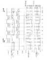
図53は、従来の液晶表示装置において用いられていた容量アレイ形のDACの構成を表す概念図である。同図に例示したDACは、いわゆるパラレル入力型のものであり、スイッチ制御回路41、基準電圧源42、スイッチ・アレイ43、容量アレイ44、リセット・スイッチ45、及びバッファ・アンプ46からなる。
【0008】
同図に表した例においては、映像信号として、(B6、B5、・・・B1)なる6ビットのデジタル・データがパラレルに入力される。
【0009】
容量アレイ44には、デジタル・データのビット数よりもひとつ多い数のコンデンサが設けられている。これらのコンデンサの容量値は、バイナリに対応して、C〜C/32までの6種類に重みづけされている。また、これらのコンデンサの一端は共通に接続され、増幅器46を介して映像信号線に接続されている。さらに、各コンデンサの他端は、スイッチ・アレイ43の各MOSスイッチによって基準電圧Vsか接地電位かに選択接続される。
【0010】
スイッチ・アレイ43の各スイッチは、各コンデンサの容量の重みづけの順序に一致した入力のバイナリ・データにより直接制御される。
【0011】
図53に表した例においては、6ビットの変換が可能である。すなわち、(B6、B5、・・・B1)なるパラレル・データが入力された場合には、出力電圧Voutは、以下の式により表される。
【0012】
【数1】
【0013】
一方、図53のDACにおいては、容量アレイ44における各コンデンサの容量をバイナリに重み付けする必要があるため、ビット教の増大と共に容量値の精度をより精密に保証しなければならない。従って、設計・製造上のマージンが厳しく、歩留まりも低下しやすい。
【0014】
さらに、図53に表したような従来のDACは、変換することができるデジタル・データのビット数が固定されてしまうという問題も有する。すなわち、扱うことができる映像信号の階調が、DACの回路構成により一定値に固定され、事後的に変更することができない。すると、例えば、パーソナル・コンピュータにおいて、表示内容に応じて表示モードを切り替えるような操作が困難となるという問題が生ずる。
【0015】
このようなことから、例えば特開平7−72822号公報には、2個の容量素子から構成されるシリアルDACを用いることが記載されている。しかしながら、この構成では、デジタル・アナログ変換と、容量素子へのアナログ信号の入力或いは容量素子からのデジタル信号の出力を別の期間で行わなければならないため、データ処理の高速化という点では限界があった。
【0016】
本発明は、以上説明した課題の認識に基づいてなされたものである。すなわち、その目的は、回路規模が小さく、良質の画像を表示し、しかも、表示階調を自由に変更することができる表示装置の駆動回路及び液晶表示装置を提供することにある。
【0017】
【課題を解決するための手段】
上記目的を達成するため、時系列に入力される複数ビットシリアルデータの各ビット信号に応じて複数の基準電圧のうちのひとつを排他的に選択し出力する基準電圧選択回路と、前記基準電圧選択回路に接続され、この基準電圧選択回路から出力される基準電圧を保持する第1の容量素子と、前記第1の容量素子に接続回路を介して接続され、前記接続回路が前記基準電圧選択回路に各ビット信号が入力される前のタイミングで短絡することにより前記第1の容量素子より分配される電荷を保持する第2の容量素子と、前記第2の容量素子に保持された電圧を表示信号として出力する出力線と、を備えたことを基本構成とする。
【0018】
すなわち、本発明の表示装置の駆動回路は、デジタル・データを入力しアナログ映像信号に変換して出力する表示装置の駆動回路であって、第1の容量と、前記デジタル・データのいずれかのビットを入力し、前記ビットの値が「1」である場合には前記第1の容量の充電電圧を第1の電圧とし、前記ビットの値が「0」である場合には前記第1の容量の充電電圧を前記第1の電圧とは異なる第2の電圧とする選択回路と、第2の容量と、前記第1の容量と前記第2の容量とを接続して両者の充電電荷を再配分して両者の充電電圧を同電圧とする接続回路と、を備え、デジタル・データの最下位ビットから最上位ビットまでの各ビット毎に前記選択回路と前記接続回路とをこの順序で動作させることにより得られた前記第1の容量または第2の容量の充電電圧を前記アナログ映像信号として出力する。
【0019】
上記基本構成を前提としつつ、本発明の第1の表示装置の駆動回路は、デジタルデータを入力してアナログ映像信号を出力するデジタル・アナログ変換回路を備えた表示装置の駆動回路であって、前記デジタル・アナログ変換回路は、時系列に入力される複数ビットデータの各ビット信号に応じて複数の基準電圧のうちのひとつを排他的に選択し出力する基準電圧選択回路と、前記基準電圧選択回路に接続され、この基準電圧選択回路から出力される基準電圧を保持する複数個の容量素子からなる入力側容量素子群と、前記入力側容量素子群の各容量素子に接続回路を介して接続され、前記接続回路を所定のタイミングで短絡することにより、前記入力側容量素子群の中の各容量素子を順次選択的に接続して前記入力側容量素子群の中の各容量素子より分配される電荷を保持する出力側容量素子と、を有する入力容量並列型の構成を有し、前記出力側容量素子に保持された電圧をアナログ映像信号として出力することを特徴とする。
【0020】
また、本発明の第2の表示装置の駆動回路は、デジタルデータを入力してアナログ映像信号を出力するデジタル・アナログ変換回路を備えた表示装置の駆動回路であって、前記デジタル・アナログ変換回路は、時系列に入力される複数ビットデータの各ビット信号に応じて複数の基準電圧のうちのひとつを排他的に選択し出力する基準電圧選択回路と、前記基準電圧選択回路に接続され、この基準電圧選択回路から出力される基準電圧を保持する入力側容量素子と、前記入力側容量素子に接続回路を介して接続され、前記接続回路を所定のタイミングで短絡することにより前記入力側容量素子を接続して前記入力側容量素子より分配される電荷を保持する複数個の容量素子からなる出力側容量素子群と、を有する出力容量並列型の構成を有し、前記出力側容量素子群の中の各容量素子に保持された電圧を選択的にアナログ映像信号として出力することを特徴とする。
【0021】
また、本発明の第3の表示装置の駆動回路は、デジタルデータを入力してアナログ映像信号を出力するデジタル・アナログ変換回路を備えた表示装置の駆動回路であって、前記デジタル・アナログ変換回路は、時系列に入力される複数ビットデータの各ビット信号に応じて複数の基準電圧のうちのひとつを排他的に選択し出力する基準電圧選択回路と、前記基準電圧選択回路に接続され、この基準電圧選択回路から出力される基準電圧を保持する複数個の容量素子からなる入力側容量素子群と、前記入力側容量素子群の各容量素子に接続回路を介して接続され、前記接続回路を所定のタイミングで短絡することにより、前記入力側容量素子群の中の各容量素子を順次選択的に接続して前記入力側容量素子群の中の各容量素子を順次選択的に接続して前記入力側容量素子群の中の各容量素子より分配される電荷を保持する複数個の容量素子からなる出力側容量素子群と、を有する入出力容量並列型の構成を有し、前記出力側容量素子群の中の各容量素子に保持された電圧を選択的にアナログ映像信号として出力することを特徴とする。
【0022】
前述した第1乃至第3の駆動回路において、前記基準電圧選択回路と前記入力側容量素子との間に接続された遮蔽回路をさらに備え、前記接続回路により前記入力側容量素子と前記出力側容量素子とが短絡される前に前記遮蔽回路により前記基準電圧選択回路と前記入力側容量素子とを遮断することにより前記入力側容量素子から前記基準電圧選択回路への電荷の逆流を阻止可能とすることができる。
【0023】
また、前記入力側容量素子と、前記出力側容量素子とは、略同一の容量値を有するものとすれば、電荷の再配分を均等に行うことができる。
【0024】
一方、本発明の第4の表示装置の駆動回路は、互いに直交配置された複数の信号線及び走査線と、前記信号線と前記走査線との交点にそれぞれ設けられた画素スイッチング素子と、を有し、mビットデータ(mは複数)に基づいて2のm乗の階調表示を行う表示装置の駆動回路であって、前記mビットデータが供給されるデータ分配回路と、前記mビットデータを順次格納し、所定のタイミングで出力するデータラッチ回路と、前記データラッチ回路からの出力を格納し、所定のタイミングで出力するガンマ補正回路と、前記ガンマ補正回路からの出力を格納し、所定のタイミングで出力する第1乃至第3の表示装置の駆動回路において用いるデジタル・アナログ変換回路と、前記デジタル・アナログ変換回路からの出力を増幅するアンプ回路と、を備えたことを特徴とする。
【0025】
一方、本発明の液晶表示装置は、前述したいずれかの表示装置の駆動回路と、前記画素スイッチング素子により制御される液晶と、を備え、前記液晶の動作しきい値が約2.5ボルトであることを特徴とする。
【0026】
または、本発明の液晶表示装置は、前述したいずれかの表示装置の駆動回路と、前記画素スイッチング素子により制御される液晶と、を備え、前記液晶の動作しきい値が約1.5ボルトであることを特徴とする。
【0027】
または、本発明の液晶表示装置は、前述したいずれかの表示装置の駆動回路と、画像観察面からみて背面側に設けられた光源と、を備えた、透過型の液晶表示装置であることを特徴とする。
【0028】
または、本発明の液晶表示装置は、前述したいずれかの表示装置の駆動回路と、画像観察面からみて背面側に設けられた反射体と、を備え、前記画像観察面側から入射する外光を前記反射体により反射させて画像を表示する反射型の液晶表示装置であることを特徴とする。
【0029】
または、本発明の液晶表示装置は、前述したいずれかの表示装置の駆動回路と、画像観察面からみて背面側に設けられた光源と、画像観察面からみて背面側に設けられた反射体と、を備え、前記光源から放出した光を透過させ、または前記画像観察面側から入射する外光を前記反射体により反射させて画像を表示することを特徴とする。
【0030】
または、本発明の液晶表示装置は、前述したいずれかの表示装置の駆動回路と、表示画素毎に設けられた画素スイッチング素子と、を備え、前記駆動回路と、前記画素スイッチング素子とは、同一基板上に設けられ、且つ前記基板上に堆積された同層の半導体層を含むことを特徴とする。
【0031】
【発明の実施の形態】
本発明によれば、3個あるいはそれ以上の容量のうちの一部の容量をデジタル・データのビットの値に対応した電位に充電した後に残りの容量との間で充電電荷の再配分を行う操作を繰り返すことにより、デジタル・データに対応したアナログ電圧を形成することができる。
【0032】
以下、図面を参照しつつ本発明の実施の形態について説明する。
図1は、本発明に至る過程で試作した映像信号駆動回路において用いられるデジタル・アナログ変換回路(DAC)を表す概略図である。
【0033】
また、図2は、その動作波形を表すタイミング・チャートである。
【0034】
さらに、図3は、このようなDACを搭載した液晶表示装置の要部概略構成を例示する概念図である。
【0035】
まず、図3を参照しつつ、本発明の液晶表示装置の構成について説明する。同図に例示した液晶表示装置は、「線順次方式」と称される形式のものであり、全ての映像信号線に対して同時に映像信号を書き込むように動作する。すなわち、画像表示部20に隣接して、映像信号駆動回路VDと走査線駆動回路SDとが同一基板上に設けられている。また、これらを構成するスイッチング素子は、同一の堆積工程により形成されたポリシリコンなどの同層の半導体層からなる。
【0036】
画像表示部20には、複数本の映像信号線27とこれに直交する複数本の走査線28とが配線され、これらの交点に画素TFT29が設けられている。TFT29のドレイン電極には、液晶容量Clcと補助容量Csとがそれぞれ接続され、表示画素を形成している。
【0037】
走査線駆動回路SDは、例えば、図示しないシフトレジスタと走査線駆動バッファとにより構成され、各々のバッファ出力が各走査線28に供給される。このようにして各走査線28に供給された走査線信号に基づいて、対応する画素のTFT29がオン・オフ制御される。
【0038】
映像信号駆動回路VDは、シフトレジスタ21とサンプリング・スイッチ24とDAC10とバッファ・アンプ(アンプ回路)50により構成されている。シフト・レジスタ21には、クロック信号(CLK−A)とトリガ信号が入力される。そして、シフトレジスタ21からの出力と、シリアルデータのサンプリング用クロックとにより、サンプリング・スイッチ24が制御される。サンプリング・スイッチ24からは、サンプル信号(Sample)と、その反転信号(/Sample)と、コントロール信号(Control)とが出力される。
【0039】
DAC10は、これらの信号に基づいて、シリアル入力されるデジタル映像信号をアナログ信号に変換して出力する。出力されたアナログの映像信号は、書き込み制御スイッチASと、バッファ・アンプ50を介して各映像信号線27に供給され、対応する画素TFT29を介して液晶容量Clcと補助容量Csとに蓄積され、所定の画像を表示する。
【0040】
次に、本発明に至る過程で試作したシリアルDACの構成について図1を参照しつつ説明する。
【0041】
まず、その入力段には、スイッチ選択回路11が設けられている。スイッチ選択回路11は、NOR1、NOR2、NOT1、NOT2により構成される。
【0042】
スイッチ選択回路11の後段には、NチャネルトランジスタM1、PチャネルトランジスタM2、容量C1、NチャネルトランジスタM4、PチャネルトランジスタM5、容量C2、及びNチャネルトランジスタM3が設けられている。
【0043】
スイッチ選択回路11は、入力されるデータ信号(Data)とコントロール信号(Control)とに応じて、トランジスタM1とトランジスタM2のいずれかを選択する。さらに詳しく説明すると、コントロール信号が、”L”(ロウ)の場合には、トランジスタM1とM2はデータ信号により排他的に選択可能となり、テータ信号が”0”ではトランジスタM1が選択され、データ信号が”1”ではトランジスタM2が選択される。
【0044】
一方、コントロール信号が”H”(ハイ)では、トランジスタM1,M2はいずれも選択されない。
【0045】
トランジスタM1は接地電位に接続され、選択回路11からの信号に応じて容量C1の電荷を放電する。また、トランジスタM2は基準電圧Vsに接続され、選択回路11からの信号に応じて容量C1を充電する。
【0046】
トランジスタM4とトランジスタM5は、サンプル信号(Sample,/Sample)を入力して、容量C1と容量C2の電気的接続状態を制御するトランスファ・ゲートを構成する。すなわち、サンプル信号(Sample)が”L”のときはトランスファ・ゲートは非導通となり、”H”のときに導通となる。一方、トランジスタM3は、リセット信号(Reset)により制御され、容量C2の電荷を放電する。
【0047】
次に、図1のDACの動作について図2を参照しつつ説明する。
ここでは、シリアル入力されるデジタル映像信号として、4ビットのデジタル・データである(1001)が入力される場合を一例として図示した。すなわち、データ信号(Data)として、「1」、「0」、「0」、「1」に対応するデジタル信号が順次入力される場合について説明する。また、ここでは、図1の容量C1とC2の容量値は等しいものと仮定する。
【0048】
まず、データ信号を入力する前の、時刻t0〜t2においては、コントロール信号(Control)は”H”に設定され、トランジスタM1とM2は共に非導通状態とされる。同時に、サンプル信号(Sample)は”L”に設定され、トランスファゲートを構成するトランジスタM4とM5は非導通状態とされる。これにより、容量C1の一端であるB点は開放状態となる。
【0049】
さらに、時刻t1〜t2において、リセット信号(Reset)は”H”に設定され、トランジスタM3を導通状態にすることにより、容量C2の一端であるA点が接地され、A点の電位Vaは0(ボルト)とされる。
【0050】
以上の動作が、シリアル映像信号を入力する前のリセット動作に対応する。
【0051】
次に、時刻t2からシリアル映像信号を順次入力してDA変換動作を開始する。
【0052】
まず、時刻t2〜t4において、最下位ビット(LSB)である「1」が入力される。これに対応して、まず、時刻t2〜t3において、コントロール信号が”L”とされてトランジスタM1とM2を選択可能とするとともに、サンプル信号が”L”とされてトランスファゲートM4、M5を非導通として、A点とB点とが電気的に遮断される。ここで、入力したデータ信号は「1」であるので、トランジスタM1が非導通、M2が導通状態になり、B点の電位VbはVs(ボルト)に設定される。つまり、容量C1は、Vs(ボルト)の電圧まで充電される。この際、A点の電位Vaは、0(ボルト)のままに保持される。
【0053】
次に、時刻t3〜t4において、コントロール信号は”H”とされてトランジスタM1とM2を共に非導通状態とし、サンプル信号は”H”とされてトランスファゲートM4、M5を導通状態にして、A点とB点とが電気的に接続され、且つB点の電位が入力データにより変動を受けないようにされる。すると、容量C1と容量C2との間で蓄積電荷の再配分が起こる。
【0054】
すなわち、時刻t3においては、B点の電位VbはVs(ボルト)に、A点の電位Vaは0(ボルト)に設定されているので、容量C1とC2の容量値が等しいとすると、時刻t4においては、
Va=Vb=1/2×”1”×Vs=Vs/2 (2)
となる。つまり、容量C1と容量C2の充電電圧は、いずれもVs/2(ボルト)となる。
【0055】
次に、時刻t4〜t6において、映像信号の次のビットである「0」が入力される。これに対応して、まず、時刻t4〜t5においては、時刻t2〜t3と同じ状態の制御信号(コントロール信号とサンプル信号とリセット信号)が入力される。つまり、トランジスタM1とM2を選択可能とし、容量C1とC2とを電気的に遮断する。ここで、データ信号として、第2ビットの「0」が入力されているので、トランジスタM1が導通、トランジスタM2は非導通状態となり、B点の電位Vb=0(ボルト)に、A点の電位Vaは時刻t4での電位Vs/2(ボルト)に維持される。つまり、容量C1の充電電圧は0(ボルト)となり、容量C2の充電電圧はVs/2(ボルト)に維持される。
【0056】
時刻t5〜t6では、時刻t3〜t4と同じ状態の制御信号が入力されることにより、容量C1と容量C2との間で、蓄積電荷の再配分が起こる。その結果として、時刻t6において、
【0057】
以降、時刻t6〜t8において映像信号の第3ビットである「0」が入力され、時刻t8〜t10において最上位ビット(MSB)である「1」が入力される。そして、これらのビット・データの入力に対応して、上述した一連の動作が繰り返される。 その結果として、時刻t10において、A点の電位VaとB点の電位Vbは、
【0058】
時刻t10以降は、コントロール信号(Control)は”H”に、サンプル信号(Sample)とリセット信号(Reset)は”L”に設定される。これによって、容量C1とC2とが電気的に遮断され、また入力デジタルデータによってトランジスタM1とM2が選択されないようにして、Vaを保持することができる。このようにして入力デジタルデータに対応したアナログ電位Vaが得られ、対応する映像信号線27に印加される。
【0059】
以上説明したように、図1に例示したシリアルDACによれば、シリアル入力されるデジタル映像信号を確実且つ容易にアナログ信号に変換することができる。しかも、DACの回路構成は極めて簡単であり、回路面積を従来よりも大幅に縮小することができる。つまり、同一の基板上に堆積した同層のポリシリコンなどの半導体層を用いて画素TFTと駆動回路のスイッチング素子を形成する際に、駆動回路の面積を縮小することができる。
【0060】
このような回路規模の縮小効果は、デジタル・データのビット数に応じて高くなり、表示画像を高画質化する程、その効果をより顕著に得ることができる。例えば、図53に例示した従来の6ビットのパラレル入力型DACと比較すると、図1のシリアルDACの回路規模は、約1/6程度と極めて小さくすることができる。つまり、回路が占める面積を従来の約1/6に縮小することができる。
【0061】
一般的なnビットのパラレル入力型DACと比較すると、図1のシリアルDACの回路規模は、およそ1/nであり、ビット数が増加するほど、回路規模の縮小効果を得ることができる。これは、駆動回路をパネルに集積させたポリシリコンTFTの液晶表示装置においては、特に有利に作用する。表示画像の高画質化するためには、表示階調すなわち、映像信号のビット数を増加する必要があるが、図1のシリアルDACによれば、回路規模を増大させず、パネルの小型化と高画質化とを両立することができる。
【0062】
さらに、図1のシリアルDACによれば、回路を変更することなく、異なるビット数のデジタル・データをアナログ映像信号に変換することができるという効果も得られる。すなわち、シリアルに入力されるデジタル・データの各ビットについて、上述したような動作を繰り返すことにより、ビット数に依存せずにデジタル・データをアナログ変換することができる。
【0063】
図1のシリアルDACが奏するこれらの効果は、特にコンピュータの表示装置などに応用する際に有利となる。すなわち、コンピュータにおいては、その用途やソフトウェアなどに応じて画像表示モードを切り替える必要がある場合が多い。その際に、表示分解能とともに表示階調すなわち階調ビット数も切り替えるようにすることが望ましい。図1のシリアルDACによれば、このような場合においても、同一のDACを用いてアナログ変換することができる。
【0064】
例えば、入力するデジタル・データのビット数に応じて、図2に例示したようなDA変換を行う期間ts〜teをさらに細かく分割することにより、さらにビット数が大きいデジタル・データをアナログ電位に変換できる。nビットのデジタル・データ(Bn、Bn−1、・・・B1)(ここで、各ビットBkは、0または1である。)を図1のDACで変換した時に得られるアナログ電位Vaは、次式により表される。
【0065】
【数2】
【0066】
以上説明したシリアルDACを、さらに概念的に説明すると以下の如くである。
【0067】
図4は、図1に例示したシリアルDACの構成を概念的に表した構成図である。すなわち、図1に例示したシリアルDACは、2つの容量C1とC2を基本構成として有する。そして、データ信号(data、/data)及びコントロール信号(/control)に基づき、容量C1に対して、デジタル信号に対応する電圧をシリアル的に入力する。一方、これと平行してサンプル信号(sample)に基づいて容量C1とC2との間で電荷の再配分を実行することにより、デジタル信号をアナログ電圧に変換する。なお、図4に表した入力電圧V+とV−は、それぞれ図1におけるVsと接地電位に対応する。
【0068】
本発明者は、このようなシリアルDACに対してさらに改良を加え、表示装置の駆動回路に搭載してさらに好適なシリアルDACを発明した。
【0069】
図5は、本発明にかかる第1のシリアルDACの基本構成を表す概念図である。
【0070】
また、図6は、図5のシリアルDACの動作を説明するタイミングチャートである。
【0071】
図5に表したシリアルDAC10Aは、1次側に1つの容量C1が設けられ、2次側には2つの容量C21及びC22が設けられた「出力容量並列型」のDACである。これら2つの容量C21、C22を交互に使い分けることにより、DA(デジタル・アナログ)変換処理と信号線への書き込みとを連続して実施することができる。
【0072】
図6のタイミングチャートを参照しつつその動作について説明すると以下の如くである。
【0073】
まず、リセット信号(RST)をオンすることにより、容量C21、C22を初期化する。
【0074】
次に、コントロール信号(/control)とサンプル信号(sample1)を交互にオンすることにより、容量C1にデジタル信号の各ビットに対応する電圧をシリアル的に印加し、同時に容量C21との間で電荷の再配分を実行する。この動作によって、デジタルデータに対応するアナログ電位が容量C21に充電される。
【0075】
次に、コントロール信号(/control)とサンプル信号(sample2)を交互にオンすることにより、容量C1にデジタル信号の各ビットに対応する電圧をシリアル的に印加し、同時に容量C22との間で電荷の再配分を実行する。この動作によって、デジタルデータに対応するアナログ電位が容量C22に充電される。
【0076】
この際に、容量C22を用いたDA変換処理と平行して容量C21から図示しない信号線に対してアナログ電位の書き込みを実行することができる。つまり、図5に表したシリアルDACによれば、容量C21とC22の一方の容量を用いてDA変換処理を実行しつつ、他方の容量から信号線への電位書き込みを平行して実施できるため、駆動回路の信号処理時間を大幅に短縮することができる。
【0077】
一般に、液晶表示装置をはじめとする各種の表示装置は、大容量化と高精細化の傾向にあり、信号線自身の寄生容量も増加する傾向にある。つまり、アナログ電位を信号線に正確に書き込むための時間も長くする必要がある。
【0078】
このような要求に対して、図5の構成によれば、DA変換処理と信号線への電位書き込み処理とを平行して実施できるので、信号処理時間を短縮しつつ、信号線に対して正確にアナログ電位を書き込むことができ、高精細で階調数が高い高品位な画像を迅速且つ正確に表示することが可能となる。
【0079】
なお、図6のタイミングチャートにおいては、3ビットのデジタルデータをDA変換する場合を例示したが、本発明は、これに限定されず、任意のビット数のデジタルデータに対して同様の処理を行うことができる。
また、後に詳述するように、シリアルDACの2次側の容量C21及びC22のそれぞれは、必ずしも特定の信号線に固定される必要はなく、切換スイッチを介して、複数の信号線のいずれかに随時切換接続可能とすることができる。本発明者の試作検討の結果によれば、例えば、容量C21とC22のそれぞれに対して、6本乃至30本程度の信号線を切換スイッチを介して適宜接続することが可能であることが判明している。このようにすれば、駆動回路に搭載するDACの数を大幅減らして、構成を小型化・簡略化することができる。
【0080】
次に、本発明にかかる第2のDACについて説明する。
【0081】
図7は、本発明にかかる第2のDACの基本構成を表す概念図である。
【0082】
また、図8は、図7のDACの動作を説明するタイミングチャートである。
【0083】
図7に表したDAC10Bは、1次側に3つの容量C11〜C13が設けられ、2次側には1つの容量C2が設けられた「入力容量並列型」のDACである。このように1次側に複数の容量を設けることにより、デジタル信号をパラレル的に入力し、これをDAC内でシリアル的にアナログ変換することができる。
【0084】
図8のタイミングチャートを参照しつつその動作について説明すると以下の如くである。
【0085】
まず、リセット信号(RST)をオンすることにより、容量C2を初期化する。
【0086】
次に、3つのコントロール信号(/control1 〜/control3)を同時にオンにすることにより、容量C11〜C13にデジタル信号の各ビットに対応する電圧をパラレル的に印加する。入力されるデジタルデータが3ビットデータの場合には、例えば、容量C11に3ビット目(最下位ビット)のデータ(data1)、容量C12に2ビット目のデータ(data2)、容量C13に1ビット目(最上位ビット)のデータ(data3)に相当する電圧がそれぞれ印加される。
【0087】
次に、サンプル信号(sample1〜sample3)を順次オンすることにより、容量C11〜C13にそれぞれ蓄積された電荷を容量C2との間で再配分する。つまりシリアル的なアナログ変換を実行する。この動作によって、容量C11〜C13に入力されたデジタルデータに対応するアナログ電位が容量C2に充電される。
【0088】
この後に、図示しないアナログスイッチや出力回路を介して容量C2に充電されたアナログ電位を所定の信号線に書き込む。
【0089】
以上説明したように、図7に表したDACによれば、1次側に複数の容量C11〜C13を設け、これらに対してデジタルデータをパラレル的に入力することができるので、デジタルデータを高速に入力できるという効果が得られる。
【0090】
なお、図7に例示した構成において、1次側の容量の数は、必ずしも入力されるデジタルデータと同一である必要はない。例えば、図7に例示したように3つの容量C11〜C13を有するDACを用いて、6ビットのデジタルデータのDA変換を実行することも可能である。具体的には、まず、1サイクル目として6ビット目(最下位ビット)〜4ビット目までのデータをそれぞれ容量C11〜C13に入力してシリアル的なアナログ変換を実行する。次に、2サイクル目として3ビット目〜1ビット目(最上位ビット)までのデータをそれぞれ容量C11〜C13に入力してシリアル的なアナログ変換を実行すれば良い。
【0091】
この具体例からも分かるように、1次側の容量の数は、必ずしも入力デジタルデータのビット数と等しい必要はないが、1次側の容量の数を入力ビット数の整数分の1とすると、効率が良い。
【0092】
一方、1次側の容量の数よりも少ないビット数のデジタルデータも同様に扱うことができる。すなわち、このような場合には、ビット数に応じた数の容量を選択して用いれば良い。
【0093】
一方、図7に表したDACにおいても、2次側の容量C2は、特定の信号線に固定される必要はなく、切換スイッチを介して、複数の信号線のいずれかに随時切換接続可能とすることができる。この点については、図5に関して前述した通りである。
【0094】
次に、本発明にかかる第3のDACについて説明する。
【0095】
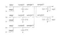
図9は、本発明にかかる第3のDACの基本構成を表す概念図である。
【0096】
また、図10は、図9のDACの動作を説明するタイミングチャートである。
【0097】
図9に表したDAC10Cは、1次側に3つの容量C11〜C13が設けられ、2次側には2つの容量C21、C22が設けられている。つまり、1次側と2次側のいずれにも複数の容量が設けられた「入出力容量並列型」のDACである。
【0098】
1次側に複数の容量C11〜C13を設けることにより、図7に関して前述したようにデジタル信号をパラレル的に高速入力することができる。一方、2次側に複数の容量C21、C22を設けることにより、図5に関して前述したように、DA変換処理と信号線への書き込みを平行して処理することができる。
【0099】
図10のタイミングチャートを参照しつつその動作について説明すると以下の如くである。
【0100】
まず、リセット信号(RST)をオンすることにより、容量C21、C22を初期化する。
【0101】
次に、3つのコントロール信号(/control1 〜/control3)を同時にオンにすることにより、容量C11〜C13にデジタル信号の各ビットに対応する電圧をパラレル的に印加する。入力されるデジタルデータが3ビットデータの場合には、例えば、容量C11に3ビット目(最下位ビット)のデータ(data1)、容量C12に2ビット目のデータ(data2)、容量C13に1ビット目(最上位ビット)のデータ(data3)に相当する電圧がそれぞれ印加される。
【0102】
次に、サンプル信号(sample1)をオンすることにより2次側の容量C21を選択する。そして、サンプル信号(sample11〜sample13)を順次オンすることにより、容量C11〜C13にそれぞれ蓄積された電荷を容量C21との間で再配分する。つまりシリアル的なアナログ変換を実行する。この動作によって、容量C11〜C13に入力されたデジタルデータに対応するアナログ電位が容量C21に充電される。
【0103】
次に、2次側の容量C22を選択して次のDA変換処理を実行する。
【0104】
すなわち、3つのコントロール信号(/control1 〜/control3)を同時にオンにすることにより、容量C11〜C13にデジタル信号の各ビットデータ(data1〜data3)に対応する電圧をパラレル的に印加する。
【0105】
次に、サンプル信号(sample2)をオンすることにより2次側の容量C22を選択する。そして、サンプル信号(sample11〜sample13)を順次オンすることにより、容量C11〜C13にそれぞれ蓄積された電荷を容量C22との間で再配分する。この動作によって、容量C11〜C13に入力されたデジタルデータに対応するアナログ電位が容量C22に充電される。
【0106】
このDA変換処理の間に、図示しないアナログスイッチや出力回路を介して容量C21に充電されたアナログ電位を所定の信号線に書き込むことができる。
【0107】
以上説明したように、図9に表したDACによれば、1次側に複数の容量C11〜C13を設け、これらに対してデジタルデータをパラレル的に入力することができるので、デジタルデータを高速に入力できるという効果が得られる。
【0108】
さらに、2次側の複数の容量C21、C22を設けることにより、DA変換処理と信号線への書き込みを同時に処理することができる。
【0109】
従って、図9に例示したDACによれば、図5乃至図8に関して前述した効果を同時に得ることができる。
【0110】
以上、本発明の駆動回路において用いるデジタル・アナログ変換回路(DAC)について具体例を参照しつつ説明したが、本発明のDACはこれらの具体例に限定されるものではない。例えば、図1乃至図9に関しては、1次側容量C1(あるいはC11など)と2次側容量C2(あるいはC21など)の容量値が同一の場合を例に挙げて説明したが、これらの容量は同一でなくても良い。1次側の容量値と2次側のの容量値とが異なる場合には、所定の「ゲイン」が得られる。具体的には、例えば、1次側容量C1の容量値をC1、2次側容量C2の容量値をC2とした場合には、式(2)〜式(5)において、右辺の係数「1/2」の代わりに、係数「C1/(C1+C2)」を適用すれば良い。例えば、容量C2が容量C1の3倍の容量値を有する場合には、この係数は「1/4」となる。また、容量C1が容量C2の3倍の容量値を有する場合には、この係数は「3/4」となる。
【0111】
従って、容量C1と容量C2の容量値を適宜選択して、所定のゲインが得られるようにすれば、基準電位Vsに対して、映像信号電圧の範囲を最適な範囲に調節することもできる。
【0112】
ところで、図1あるいは図5に表した具体例においては、DACに対してシリアル・データが入力される場合について説明した。しかし、本発明は、これに限定されるものではなく、パラレル入力されるデジタル・データを変換することも可能である。このためには、例えば、パラレル入力されるデジタル・データを蓄積し、その最下位ビットから順次各ビットのデータを取りだして供給する手段を別途設ければ良い。このようにして、パラレル入力されるデジタル・データについても、図2に関して前述したような動作を繰り返すことにより同様にアナログ変換することができる。この場合には、回路規模は、若干大きくなるものの、任意長のデジタル・データに対応することができるという本発明の効果は同様に得ることができる。
【0113】
また、容量C1、C2を放電させるための接地電位に変えて、第2の基準電位を設けても良い。この場合には、得られるアナログ映像信号の下限電圧が、第2の基準電位と同じ電圧となる。
【0114】
また、図1乃至図9に例示した具体例においては、第2の容量C2の充電電圧をアナログ映像信号として出力する構成を表したが、本発明は、これに限定されるものではない。すなわち、図1あるいは図5の構成においては、最上位ビットまでの一連の充電・電荷再配分の動作が終了した時点においては、第1の容量C1と第2の容量C2の充電電圧は同一の値であるので、第2の容量C2の代わりに第1の容量C1の充電電圧をアナログ映像信号として外部に出力するような選択回路を設けても良い。
【0115】
さらに、第1の容量C1と第2の容量C2とを短絡した状態で、いわば出力容量C1+C2の充電電圧をアナログ映像信号として外部に出力しても良い。このようにすれば、外部回路の寄生容量によるDAC出力電圧の変動を半減できるという効果が得られる。
【0116】
次に、本発明の駆動回路において用いて好適なシリアル型DACの変型例について説明する。
【0117】
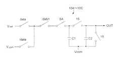
図11は、図1乃至図9に例示したシリアル型DACをさらに簡略化しつつ変型した概略回路図である。すなわち、シリアル型DACは、2つのレベルの電圧VrefとVcomとを相補的に切り替えるスイッチdata(図1のトランジスタM2に対応する)及び/data(図1のトランジスタM1に対応する)と、遮断スイッチ/SW1と、容量C1及びC2と、これらの間に設けられた連結スイッチ16と、リセットスイッチ18とを有する。
【0118】
図11の変型例においては、遮断スイッチ/SW1を設けることにより、容量C1からの蓄積電荷の逆流を確実に防止することができる。
【0119】
さらに、図1乃至図11のDAC回路においては、リセットスイッチ18のオフ時リーク量が他のスイッチに比べて小さくなるように形成することが望ましい。これは、容量C2の蓄積電荷のリークを防止するためである。このためには、リセットスイッチ18を構成するトランジスタのゲート長Lを長く、ゲート幅Wを短く形成し、ダブルゲート構造とすることが有利である。
【0120】
また、同様に容量C1の蓄積電荷の変動を防止するためには、遮断スイッチ/SW1もオフ時のリーク量が小さいことが望ましい。このためには、やはり遮断スイッチ/SW1を構成するトランジスタのゲート長Lを長く、ゲート幅Wを短く形成し、ダブルゲート構造とすることが有利である。
【0121】
またこれと関連して、遮断スイッチ/SW1のオン期間を、連結スイッチ16のオン期間よりも長く設定することが望ましい。これは、遮断スイッチ/SW1をリーク量の小さいトランジスタにより構成した場合には、電圧書き込み時間を長くする必要があるからである。
【0122】
一方、図3に例示したような表示装置において画素のスイッチング素子を構成するTFT29は、−2ボルト及び12ボルト電源を用いる場合が多い。従って、図1乃至図11に例示したDACの各スイッチも、−2ボルト及び12ボルト電源を用いてオフ条件を画素TFTと同等とすると、電源構成を簡略化することができる。
【0123】
図12は、本発明の駆動回路に用いて好適なDACの第2の変型例を表す概略回路図である。すなわち、同図の回路においては、遮断スイッチ/SW1と直列にスイッチSAが設けられている。スイッチSAは、遮断スイッチ/SW1と連結スイッチ16とのNAND論理に基づいて動作させる。つまり、遮断スイッチ/SW1と連結スイッチ16が共に半開きのような状態においては、スイッチSAがオフするように動作させる。このようなスイッチSAを設けることにより、スイッチ/SW1とスイッチ16の動作タイミングの「ずれ」による容量C1への誤った電圧書き込みを確実に防止し、DACの変換動作を高精度化できる。
【0124】
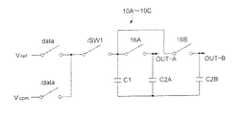
図13は、本発明の駆動回路に用いて好適なDACの第3の変型例を表す概略回路図である。すなわち、同図の回路においては、2次側の容量として容量C2Aと容量C2Bの2つの容量が並列に設けられている。これら2つの容量のそれぞれは、連結スイッチ16A、16Bを介して1次側容量C1と相補的に接続される。つまり、ひとつのDA変換処理を容量C1と容量C2Aとの間で行い、次のDA変換処理は、容量C1と容量C2Bとの間で行うようにする。なお、図13においては省略したが、2次側容量C2AとC2Bには、それぞれリセットスイッチを設けることが望ましい。
【0125】
このように、2次側の容量として容量C2AとC2Bの2つを設け、DA変換処理毎に切り替えて用いることによって、2次側容量の一方から信号出力回路50にアナログデータを出力する間にも、2次側容量のもう一方を用いて次のDA変換処理を開示でき、データ処理を高速化できる。
【0126】
もうひとつのメリットとして、隣接するDAC間で1次側容量と2次側容量の容量比C2/C1に「ばらつき」があるような場合に、「誤差拡散」の効果が得られる。
【0127】
図14は、「誤差拡散」の効果を説明するための概念図である。すなわち、同図(a)に表した例においては、信号線Nに対応するDACは2次側容量C2を有し、隣接する信号線(N+1)に対応するDACは2次側容量C2’を有する。さらにこれらのDACは、ふたつめの2次側容量として容量C2Bを共有している。そして、同図の右側に表したように、信号線NのDACは第1、3、4フレームにおいて容量C2を用い、第2フレームにおいては容量C2Bを用いる。一方、信号線(N+1)のDACは、第1、2、4フレームにおいては容量C2’を用い、第3フレームにおいては容量C2Bを用いる。
【0128】
このようにすれば、容量C2とC2’との間に容量の「誤差」がある場合にも、容量C2Bを共用することによって、この「誤差」を時間的に拡散させて目立ちにくくすることができる。
【0129】
さらに、本発明においては、図14(b)に例示したように、2次側容量を新たに追加せずに、隣接したDAC間で利用しあうことも可能である。すなわち、同図に表した具体例においては、信号線Nに対応するDACは2次側容量C2を有し、隣接する信号線(N+1)に対応するDACは2次側容量C2’を有する。そして、それぞれのDACは、フレーム毎に、2次側容量を交換しあってDA変換処理を実行する。このようにしても、容量C2とC2’との間の容量の「誤差」を時間的に拡散させ、目立ちにくくすることができる。
【0130】
以上、本発明の駆動回路に用いて好適なシリアル型DACについて詳細に説明した。
【0131】
次に、本発明の駆動回路においてDACから出力された映像信号を映像信号線に出力する信号出力回路(アンプ回路)について詳細に説明する。
【0132】
図3に関して前述したように、本発明による映像信号線駆動回路は、映像信号線27毎にDAC10A〜10C、アナログスイッチAS、映像信号出力回路50が直列に接続された構成を有する。
【0133】
図15は、本発明の1実施形態にかかる映像信号線駆動回路の要部を表す概略図である。すなわち、同図は、映像信号線27の1本について、DACとアナログスイッチASと映像信号出力回路50Aとが接続された状態を表す回路図であり、図1乃至図14に関して前述したものと同等の要素には同一の符号を付して詳細な説明は省略する。
【0134】
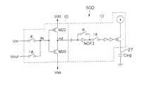
信号出力回路50Aは、スイッチS1〜S4と、容量C3と、NOT3、NOT4及びNOT4とトランジスタM4及びM5とに構成される。トランジスタM4とM5は、NOT3〜5とにより選択的に選択される。このような出力回路50を用いることにより、スイッチング動作を制御する反転増幅器動作点電圧を検出してTFT特性のバラツキの影響を軽減でき、良好な画像を提供できる。
【0135】
図16は、図15の回路における動作波形を表すタイミングチャートである。図16を参照しつつ、信号出力回路50Aの動作について説明すると以下の如くである。
【0136】
まず、時間t1〜t10までの期間は、DAC10A〜10Cによるシリアル的なデジタル・アナログ(DA)変換が実行される。この変換動作については、図1乃至図10に関して詳細に前述した通りであるので詳細な説明は省略する。そして、t10においてDA変換が終了すると、信号線出力回路の動作が開始する。
【0137】
まず、時間t11において、制御信号ENABLEが”H”になることにより、アナログスイッチASがオンする。すると、A点とC点が電気的に接続される。ここで、時間t11−t12においては、制御信号CLKは”L”なので、スイッチS2とスイッチS3が導通状態になり、スイッチS1とS4は非導通状態となる。その結果として、静電容量C3の一端D点の電位Vdは映像信号線電位Vsigとなり、もう一端E点の電位VeはS3によりインバータNOT3の入出力が短絡されるので、NOT3の動作点電位Vopとなる。ここで、NOT3の動作点電圧は、回路を構成するTFT特性により異なるので、映像信号線駆動回路に応じて異なる。
【0138】
次に時間t12〜t13においてCLKが”H”になると、スイツチS1とS4が導通状態となり、スイツチS2とS3は非導通状態となる。このため、D点の電位Vd=Vc=Vaとなり、DAC10A〜10Cの出力電位と等しくなる。一方、E点の電位Veは、CLKが”L”状態の電位をC3が保持するため、Ve=(Va−Vsig)+Vopとなる。よって、F点の電圧Vfは、
(1)Va>Vsigの場合は、Vf=0
(2)Va<Vsigの場合は、Vf=VDD
となる。
【0139】
本具体例の場合は、時間t11においてVa>Vsig であるので、F点の電位Vfはゼロとなる。その結果として、PチャネルトランジスタM5が導通状態になり、電流Ipが映像信号線27に供給される。この時、期間Tの間における映像信号線27の電圧上昇分△Vpは、信号線容量をCsig とすると、△Vp=1p×T/Csig と表される。
【0140】
上記動作が複数回行われて時間t26になると、Va<Vsig となるのでNチャネルトランジスタM4が導通状態となり、電流Inが映像信号線27からGNDに流れる。この時、期間Tの間に変化する電位△Vnは、△Vn=In×T/Csig と表される。
【0141】
時刻t26以降は、映像出力期間中でVsig は、Va近傍において△Vpと△Vn の幅で変化し続ける。そして、最終的に形成される映像信号線電位Vsig の誤差電圧Verr は、Verr=|△Vp−△Vn|/Tとなる。ここで、△VpはトランジスタM5の特性に依存し、△VnはトランジスタM4の特性に依存するが、CLKの周波数を十分高く設定することにより、Verr を無視しうるレベルまで小さくできる。
【0142】
以上説明したように、本発明の映像信号線駆動回路の信号出力部は、DAC10A〜10Cの出力電圧と映像信号線27の電圧との比較に用いるインバータの動作点電圧バラツキを静電容量C3によりキャンセルできる。さらに、制御信号CLKの周波数を十分高く設定することにより、映像信号線27に電流を直接供給するTFTの特性のバラツキをも低減できる。その結果として、表示ムラの少ない均一で良好な画像を提供できる。
【0143】
なお、図16においては、DA変換動作における時間ステップt1〜t10と、信号出力動作における時間ステップt11〜t27が略同一の場合を例示したが、本発明はこれに限定されるものではなく、DA変換動作における時間ステップと、信号出力動作における時間ステップとは、互いに異なるものであっても良い。
【0144】
次に、本発明の映像信号駆動回路に用いてさらに好適な映像信号出力回路50について説明する。
【0145】
図17は、本発明において用いて好適な映像信号出力回路50Bの概念構成を表す回路図である。
【0146】
本変型例の出力回路(アンプ回路)50Bによっても、TFT特性のばらつきに影響されにくく小規模で高精度な出力アンプを提供することができる。
【0147】
すなわち、出力回路50Bは、トランジスタM6〜M10により構成される入力比較回路IDと、容量C3、NOT3、スイッチS6〜S8、トランジスタM11及びM12から構成される反転増幅出力回路IOとを有する。DAC10A〜10Cからの出力は、アナログスイッチを介してVinに入力される。また、出力回路50Bからの出力は、出力端Voutをから信号線27に出力される。
【0148】
この出力回路50Bにおいては、スイッチS5を介してDAC10A〜10Cを信号線27に接続し、信号線27の電位とDACからサンプリングされたアナログ映像電位を入力比較回路IDにより比較し、両電位が一致したら前記スイッチS6がオフにされる。
【0149】
図18は、出力回路50Bの動作を説明するためのタイミングチャートである。
【0150】
同チャートにおいてT1の期間は、スイッチS5、S6、S8がオンで、スイッチS7がオフとなる。この状態において、nd点には、入力比較回路IDに対する2入力すなわちIN−とIN+とが等しい状態での電位Vevenが保持される。一方、n1点には反転増幅回路の回路閾値Vinvが保持される。
【0151】
一方、T2の期間には、スイッチS7がオンで、スイッチS5、S6、S8がオフとなる。この状態においては、2入力すなわちIN−とIN+との間に電位差が生ずる。その結果として、nd点の電位は(Veven+△V)まで上昇する。また、n1点の電位も(Vinv+△V)に上昇する。その結果として、n2点がL出力となり、映像信号線がVddによって充電されて電位が上昇する。
【0152】
すると、IN+が上昇し、IN+=IN−(=Vin)となると再びnd点はVevenとなる。これと共に、n1点の電位はVinvに戻り、n2点はHレベルに上昇し、映像信号線27の充電が終了する。
【0153】
以上の説明からも分かるように、一連の動作については、回路を構成するTFTの閾値ばらつきに起因する制約は殆ど無い。例えば、T1の期間において入力比較回路IDの2入力(IN−とIN+)が等しいとき、nd点の電位は閾値ばらつき程度の異なった値をとりうるが、回路動作上は問題とはならない。
【0154】
さらに、本変型例においては、DAC10A〜10Cからの入力IN−は、入力比較回路IDのTFTのゲートに入力される。TFTのゲートの容量は、一般にフェムトファラッド(fF)のオーダであり、一方DAC10A〜10Cの蓄積容量C2は一般にピコファラッド(pF)のオーダである。
【0155】
一般には、出力回路の入力容量がDACの出力容量の10%程度以下であれば、製造プロセスの変動などによって出力回路の入力容量が例えば10%程度ばらついたとしても、そのばらつきは、DACの出力容量に対して10%×0.1=1%程度となり、事実上許容しうるレベルとなる。
【0156】
これに対して、本変型例によれば、DAC10A〜10Cの出力容量に対して出力回路50の入力ゲート容量は、3桁近く小さいので、出力回路50を接続したことによるDACの蓄積容量の再配分を防止し、アナログ出力の「ずれ」を解消することができる。
【0157】
また、本変型例における容量C3の容量は0.2pF程度であり、出力回路50B全体の面積は、デザインルールを5μmとした場合でも70×300μm2程度と十分に小型化することができる。
【0158】
また、出力の電流源は、アンプの動作範囲によっては、VddのみまたはVssのみとすることができ、構成を簡略化することができる。
【0159】
また、電流源を定電流源とすると、入力電圧に対する出力ばらつきをほぼ一定の小さいレベル(=ディレイ時間×定電流/Csig)に抑制できる。
【0160】
さらに、図17に例示した回路において、NOT3の出力n2の反転信号を生成してn3とし、n3とVoutとの間に抵抗と容量を直列に挿入すれば発振を防止できる。
【0161】
また、入力比較回路の2入力(IN−とIN+)の微小なずれに対して、容量C3の入力(図17においてはnd)が大きく振れるようにすれば、出力回路50Bをさらに高精度に高出力化することができる。このために、ndとC3との間に図示しない増幅回路をさらに設けてもよい。
【0162】
また、図17において、IN−とIN+とを入れ替えて、容量C3をneに接続してもよい。
【0163】
ところで、図17に例示した出力回路50Bのひとつの特徴は、
(1)入力比較回路IDにおいて入力信号(IN−とIN+)をTFTのゲートに入力する点と、
(2)入力比較回路IDからの出力信号が入力信号に対して一義的な関係を有する、すなわち、ある入力信号に対応してひとつの出力信号のみが存在する、点にある。
【0164】
これらの特徴を有する入力比較回路IDは、図17に例示したものには限定されない。
【0165】
図19は、出力回路50Bの変型例を表す概略回路図である。同図についても、図1乃至図18に関して前述した部分と同等の要素には同一の符号を付して詳細な説明は省略する。
【0166】
図19の出力回路(アンプ回路)50Cにおいては、入力比較回路IDは図17に例示したものと同様であり、いわゆる「エミッタ(ソース)結合型」の増幅器の構成を有する。但し、信号入力が異なる。そして、その動作に際しては、符号φで総称したスイッチ群と、符号/φで総称したスイッチ群とが交互にオン・オフする。
【0167】
まず、符号φで総称したスイッチ群がオンの状態において、図示しないDACからの信号VinがIN−に入力され、同時にNOT3を構成するインバータの動作しきい値の電位が容量C3の両端に保持される。
【0168】
次に、符号/φで総称したスイッチ群がオンとなる。この時に、仮にVout<Vin とすると、ndは低下する。そして、ノードSはLレベルとなり、信号線27すなわち等価容量Csigに電流書き込みが実行される。そして、信号線容量Csigの電位がVout=Vinに達し、またはそれ以上となると、ノードSはHレベルとなり、Csigの電位の上昇は停止する。
【0169】
図19に例示した出力回路50Cにおいても、入力信号を入力比較回路IDのTFTのゲートに入力するので、図17に関して前述したように、DACの2次側容量の再配分を防ぐことができる。
【0170】
また、出力回路50Cの入力比較回路IDは、入力電位IN−に対して、出力ndが一義的な関係を有する。
【0171】
図20は、入力比較回路IDの入力電位IN−と出力ndとの関係を表すグラフ図である。同図に表したように、入力と出力とが一義的な関係を有するので、NOT3やVbiを適宜設定することによって、出力回路50Cの出力特性を確実且つ容易に制御することが可能となる。
【0172】
図21は、出力回路50Bの第2の変型例を表す概略回路図である。同図についても、図1乃至図20に関して前述した部分と同等の要素には同一の符号を付して詳細な説明は省略する。
【0173】
図21の出力回路(アンプ回路)50Dにおいては、入力比較回路IDがいわゆる「相補型」の増幅回路の構成を有する。すなわち、相補トランジスタとしてのnチャネルトランジスタM20とpチャネルトランジスタM22のゲートが共通接続されて入力端とされている。従って、図17に関して前述したように、DACの2次側容量の再配分を防ぐことができる。
【0174】
また、この出力回路50Dにおいても、符号φで表したスイッチと符号/φで表したスイッチとを交互にオンさせることにより、信号線27にDACからの映像電位を書き込むことができる。
【0175】
図22は、出力回路50Dの入力比較回路IDの入力と出力との関係を表すグラフ図である。同図に表したように、「相補型」の増幅器としての入力比較回路IDにおいても、入力に対して出力が一義的な関係を有する。
【0176】
従って、VddやVss、あるいはnチャネルトランジスタM20やpチャネルトランジスタM22のサイズすなわちゲート幅やゲート長などを調節することにより、出力回路50Dの出力特性を精密に制御することが可能となる。
【0177】
図23は、出力回路50Bの第3の変型例を表す概略回路図である。同図についても、図1乃至図21に関して前述した部分と同等の要素には同一の符号を付して詳細な説明は省略する。
【0178】
図23に表した出力回路(アンプ回路)50E〜50Gにおいては、入力比較回路IDとして、負荷と駆動用トランジスタとを直列に接続した一般的な増幅回路の構成を有する。すなわち、ゲートに電圧Vbiあるいはndが入力されたトランジスタ(図23(a)においては、符号M24を付した)が負荷として作用し、ゲートにVinまたはVoutが入力されるトランジスタが駆動用トランジスタとして作用する。
【0179】
これらの回路においても、トランジスタの低容量なゲートに信号が入力されるので、図17に関して前述したように、DACの2次側容量の再配分を防ぐことができる。また、符号φで表したスイッチと符号/φで表したスイッチとを交互にオンさせることにより、信号線27にDACからの映像電位を書き込むことができる。
【0180】
図24は、出力回路50E〜50Gの入力比較回路IDの入力と出力との関係を表すグラフ図である。同図に表したように、これらの入力比較回路IDにおいても、入力に対して出力が一義的な関係を有するので、Vbiやトランジスタのサイズなどを調節することにより、出力回路50E〜50Gの出力特性を精密に制御することが可能となる。
【0181】
図25は、出力回路50Bの第4の変型例を表す概略回路図である。同図についても、図1乃至図23に関して前述した部分と同等の要素には同一の符号を付して詳細な説明は省略する。
【0182】
図25の出力回路(アンプ回路)50Hにおいては、入力比較回路IDは、図17や図19と同様の「エミッタ(ソース)結合型」の増幅器の構成を有する。但し、本変型例においては、反転増幅回路が2系統設けられている。
【0183】
出力回路50Hの動作について説明すると、以下の如くである。
【0184】
まず、サンプリング期間においては、符号φで総称したスイッチ群がオンとなり、他のスイッチはオフとなる。この状態において、ndには、入力比較回路IDの入力が、それぞれ、IN−=Vcom、IN+=Vin(すなわちDACの出力)となっている時の電位Vinitが保持される。また、n1Aとn1Bには、それぞれ反転増幅回路を構成するインバータNOT3A、NOT3Bの回路しきい値Vinvが保持される。
【0185】
次に、信号線に対する書き込み期間においては、符号/φで総称したスイッチ群がオンとなり、他のスイッチはオフとされる。この状態においてVout<Vinの場合について説明すると、まず、IN+=Vout(=信号線電位)となっているためにndは(Vinit+ΔV)となり、n1も(Vinv+ΔV)となる。すると、n2Aは低下し、n3AはLレベルとなり、トランジスタMPがオンする。これにより、信号線27は、Vddによって充電され、Csig電位(すなわちVout)はVddに近づき、ΔVは次第にゼロになる。
【0186】
ΔV=0となると、n1AはVinvに復帰し、n3AはHレベルとなり、トランジスタMPはオフとなって信号線電位は保持される。
【0187】
一方、Vout>Vinの場合には、C1B、n1B、n3Bが同様の動作をすることにより、Vssに向かってVsigが放電されて所望の電位に達した後、信号線電位が保持される。
【0188】
本変型例においては、出力回路50HがDAC出力を参照するのはサンプリング期間のみである。信号線書き込み期間には、DACは次の行の信号電位のDA変換を平行して行うことができる。また、本変型例においても、出力回路の入力容量が小さく、TFTの特性に影響されない安定したサンプリング出力が可能となる。
【0189】
図26は、出力回路50Bの第5の変型例を表す概略回路図である。同図についても、図1乃至図25に関して前述した部分と同等の要素には同一の符号を付して詳細な説明は省略する。
【0190】
図26の出力回路(アンプ回路)50Iにおいても、入力比較回路IDは、図17や図19あるいは図25と同様の「エミッタ(ソース)結合型」の増幅器の構成を有する。但し、本変型例においては、反転増幅回路が1系統であり、出力トランジスタMPにスイッチ/φ1が接続され、出力トランジスタMNにはスイッチ/φ2が接続されている。
【0191】
出力回路50Iの動作について説明すると、以下の如くである。
【0192】
まず、サンプリング期間においては、符号φで総称したスイッチ群がオンとなり、他のスイッチはオフとなる。この状態において、ndには、入力比較回路IDの入力が、それぞれ、IN−=Vcom、IN+=Vin(すなわちDACの出力)となっている時の電位Vinitが保持される。また、n1は、反転増幅回路を構成するインバータNOT3の回路しきい値Vinvが保持される。
【0193】
次に、第1の信号線に対する書き込み期間においては、符号/φで総称したスイッチ群とスイッチ/φ1がオンとなり、スイッチφ、/φ2はオフとされる。この状態においてVout<Vinの場合についてのみ信号線容量CsigがVssによってVout=Vinとなるところまで充電される。Vout>Vinの場合は、充電は行われない。
【0194】
また、第2の信号線に対する書き込み期間においては、符号/φで総称したスイッチ群とスイッチ/φ2がオンとなり、スイッチφ、/φ1はオフとされる。この状態においてVout>Vinの場合についてのみ信号線容量CsigがVssによってVout=Vinとなるところまで充電される。Vout<Vinの場合は、充電は行われない。
【0195】
本変型例においても、出力回路50IがDAC出力を参照するのはサンプリング期間のみである。信号線書き込み期間には、DACは次の行の信号電位のDA変換を平行して行うことができる。また、本変型例においても、出力回路の入力容量が小さく、TFTの特性に影響されない安定したサンプリング出力が可能となる。つまり、サンプリングラッチやデジタルラッチの数が少なく、且つDAC出力を高精度に増幅して信号線に書き込む信号線駆動回路を実現することができる。
【0196】
なお、図25及び図26に例示した具体例においては、いわゆるN−TOP型差動増幅段を採用しているが、出力電圧レンジに応じてP−TOP型差動増幅段を用いても良い。
【0197】
以上、説明した出力回路50A〜50Iは、信号線の電位とDACの電位とをサンプリング比較し、信号線に充電を行うものであった。
【0198】
しかし、本発明の駆動回路は、このような出力回路には限定されず、アナログ的に信号線の充電を行う出力回路も用いることができる。
【0199】
図27は、本発明において用いることができる負極性用の出力回路50Jを表す回路図である。出力回路(アンプ回路)50Jは、スイッチSW1〜SW8、インバータINV1、INV2、トランジスタQ1を有する。また、容量C2は、後に詳述するように、DACの2次側容量と共用することが可能である。
【0200】
スイッチSW6の一端は容量C2の他端に接続され、スイッチSW6の他端は電圧Vdd(例えば、10V)に接続されている。スイッチSW5の一端は前端インバータINV1の入力端子に接続され、スイッチSW5の他端は前段インバータINV1の出力端子に接続されている。スイッチSW7の一端は前段インバータINV1の出力端子に接続され、スイッチSW7の他端は後段インバータINV2の入力端子に接続されている。スイッチSW8の一端は後段インバータINV2の入力端子に接続され、スイッチSW8の他端は電圧VSS(例えば、0V)に接続されている。
【0201】
そして、容量C2は差分電圧保持回路を構成し、電圧VDDの電圧源と定電流回路I1とが信号線27の電圧を一定割合で変化させる電圧変更回路を構成し、スイッチSW3が入力電圧設定回路を構成し、スイッチSW5の帰還ループがしきい値電圧設定回路を構成している。
【0202】
図28は、図27の出力回路50Jの各部のタイミング図である。以下、このタイミング図を用いて出力回路50Jの動作を説明する。
【0203】
まず、時刻T21〜T22の期間(リセット期間)内に、スイッチSW4、SW6、SW8をオンにし、スイッチSW1〜SW3、SW5、SW7をオフにする。これにより、信号線27の電圧(図26のd点)は、電圧VSSと同じ電圧(例えば、0V)になる。また、前段インバータINV1の入力端子の電圧は、電圧VDDと同じ電圧(例えば、10V)になり、後段インバータINV2の入力端子の電圧は、電圧VSSと同じ電圧(例えば、0V)になる。ここで、前段インバータINV1の入力端子の電圧を電圧VDDにし、後段インバータINV2の入力端子の電圧を電圧VSSにするのは、前段インバータや後段インバータを構成するCMOSトランジスタに貫通電流が流れないようにするためである。すなわち、CMOSトランジスタを構成するp型MOSトランジスタとn型MOSトランジスタのうちの一方のMOSトランジスタを十分なオフ状態にすることにより、貫通電流が流れないようにしている。これにより、この出力回路50Jにおける電力消費の低減を図れる。したがって、前段インバータINV1の入力端子と後段インバータINV2の入力端子に印加する電圧は、電圧VDD(例えば、10V)と電圧VSS(例えば、0V)のいずれでもよい。
【0204】
次に、時刻T22〜T23の期間(2次側容量C2への書き込み期間)内に、スイッチSW3、SW5をオンしして、スイッチSW1、SW2、SW4、SW6〜SW8をオフにする。これにより、a点の電圧はDACからの入力映像信号Vinの電圧に略等しくなる。図27では、入力映像信号Vinの電圧が3Vである例を示している。但し、スイッチSW1がオフであるので、信号線27の電圧は0Vを維持する。
【0205】
また、スイッチSW5がオンであるため、b点の電圧は前段インバータINV1のしきい値電圧(ここでは、5Vとする)に略等しい電圧に設定される。すなわち、前段インバータINV1の出力を入力にフィードバックすることにより、前段インバータINV1の入力端子及び出力端子の電圧は、前段インバータINV1のしきい値電圧に略等しい電圧に設定される。したがって、容量C2には、入力映像信号Vinの電圧(例えば、3V)と前段インバータINV1のしきい値電圧(例えば、5V)の差分電圧(例えば、2V)が保持される。
【0206】
次に、時刻T23以降(書き込み期間、安定期間)は、スイッチSW1、SW2、SW7をオンして、スイッチSW3〜SW6、SW8をオフにする。時刻T3の時点では、a点は3Vであるのに対し、d点は0Vである。このため、スイッチSW1がオンすると、a点の電圧がd点に引きづられて低下する。容量C2は上述した差分電圧(2V)を維持しているので、この容量C2の他端側であるb点の電圧もa点の電圧に追随して低下し、論理回路LCの出力が反転してローレベル(例えば、0V)になる。これにより、トランジスタQ1がオンし、一定の電流が定電流回路I1からトランジスタQ1とスイッチSW2を介して信号線27に供給される。このため、信号線27(d点)の電圧は一定の傾きdtで上昇する。
【0207】
信号線27の電圧が一定の傾きdtで上昇すると、それに応じてa点、b点の電圧も一定の傾きdtで上昇する。やがて、時刻T4になると、信号線27の電圧が入力映像信号Vinの電圧である3Vに等しくなり、a点の電圧も3Vに等しくなる。容量C2は上述した差分電圧(2V)を保持しているので、図26のb点の電圧は前段インバータINV1のしきい値電圧である5Vになる。このため、論理回路LCの出力が再び反転してハイレベル(例えば、10V)になる。これにより、トランジスタQ1がオフとなり、定電流回路I1から信号線27への電流供給、つまり電圧の供給は遮断される。このような動作により、信号線27は入力映像信号Vinの電圧に略等しい3Vに設定される。
【0208】
次に、出力回路50Jを正極性用に変型した具体例について説明する。
【0209】
図29は、正極性用の出力回路50Kの詳細構成を示す回路図である。同図に表したように、正極性用の出力回路(アンプ回路)50Kは、トランジスタQ1がn型である点と、定電流回路I1が電圧VSSに接続されている点とが、図27の負極性用の出力回路50Jと異なる。これら以外の点は、上述した負極性用の出力回路50Jと同様であるので、その詳しい説明は省略する。
【0210】
以上のように、図27乃至図29に関して説明した出力回路50J、50Kによっても、信号線27を入力映像信号Vinの電圧に略等しく設定することができる。
【0211】
また、前段インバータINV1のしきい値電圧と入力映像信号Vinの電圧の差分電圧を容量C2に保持させた後に、信号線27に入力映像信号Vinを供給するので、前段インバータINV1のしきい値電圧にばらつきがあっても、信号線27の電圧はその影響を受けないようにすることができる。
【0212】
さらに、出力回路50J、50Kによれば、信号線27に電圧VDDを供給する際に定電流回路I1を介して供給するようにしたので、入力映像信号Vinの電圧や信号線27の電圧にかかわらず、一定の傾きdtで信号線Sの電圧を引き上げることができる。このため、出力回路50J、50Kのリニアリティーを確保することができ、いわゆる書き込みエラーを生じないようにすることができる。
【0213】
また、出力回路50J、50Kによれば、容量C2が保持すべき差分電圧を容量C2に設定する際に、前段インバータINV1のしきい値電圧と入力映像信号Vinの電圧とを、同一サイクルでサンプリングすることとしたので、これら2つの電圧の設定を別々のサイクルで行う場合と比べて、正確な差分電圧の設定をすることができる。
【0214】
なお、上記具体例に示す各種スイッチは、トランスファーゲートやアナログスイッチを用いて構成することができる。また、上記具体例では、入力された信号を反転増幅するインバータを2段直列的に接続して論理回路LCを構成する例を説明したが、トランジスタを組み合わせて構成されるものであれば、論理回路LCの内部構成に特に制限はない。
【0215】
次に、本発明の駆動回路において用いることができるさらに別の出力回路について説明する。
【0216】
図30は、出力回路50Lの回路図である。出力回路(アンプ回路)50Lは、信号線の電圧を制御する反転増幅回路の各インバータの入力端子の電圧を、各インバータのしきい値電圧に略等しく設定しておくことにより、各インバータのしきい値電圧にばらつきが生じていても、信号線の電圧を所望の電圧に制御することができるようにしたものである。
【0217】
すなわち、出力回路50Lのそれぞれは、図30に示すように、スイッチSW1〜SW3と、前段インバータINV1と中段インバータINV2と後段インバータINV3とからなる反転増幅回路IAと、容量C2とを、備えている。この出力回路50Lにより駆動される信号線27には、画素表示用のTFT、液晶容量および補助容量等が接続されており、同図では簡略化のため、信号線27の負荷を等価的に抵抗RとキャパシタCsigとで表している。
【0218】
スイッチSW1の一端は信号線27に接続され、スイッチSW1の他端はスイッチSW3の一端と容量C2の一端に接続されている。スイッチSW3の他端はDACから出力される入力映像信号Vinの入力端子に接続されている。容量C2の他端は、反転増幅回路IAの入力端子に接続されている。反転増幅回路IAの出力端子は、スイッチSW2の一端に接続されている。スイッチSW2の他端は、上述した信号線27に接続されている。
【0219】
反転増幅回路IAは、前段インバータINV1と中段インバータINV2と後段インバータINV3とを、直列的に接続することにより構成されている。スイッチSW1〜SW3は、図示しないスイッチ切換制御回路により切換制御される。
【0220】
なお、反転増幅回路IAが信号線電圧制御回路を構成し、容量C2が第1差分電圧保持回路を構成し、スイッチSW3が第1差分電圧設定回路を構成する。
【0221】
図31は、出力回路50L内の各部のタイミング図である。以下、このタイミング図を用いて出力回路50Lの動作を説明する。
【0222】
まず、時刻T11〜T12の期間(サンプリング期間)内に、スイッチSW3をオンにして、それ以外のスイッチであるスイッチSW1、SW2をオフにする。これにより、a点の電圧は、入力映像信号Vinの電圧に略等しくなる。図31では、入力映像信号Vinの電圧が3Vである例を示している。但し、スイッチSW1がオフであるので、信号線27(d点)の電圧は、時刻T11以前に供給された電圧を維持する。図31の例では、7Vを維持する。
【0223】
ここで、上述したように、前段インバータINV1のしきい値電圧が5.5Vであり、中段インバータINV2のしきい値電圧が4.5Vであり、後段インバータINV3のしきい値電圧が5Vであると仮定すると、何らかの手段により、この前段インバータINV1の入力端子の電圧を5.5Vに設定し、中段インバータINV2の入力端子の電圧を4.5Vに設定し、後段インバータINV3の入力端子の電圧を5Vに設定する。つまり、インバータINV1〜INV3の入力端子の電圧を、インバータINV1〜INV3のそれぞれのしきい値電圧に略等しく設定する。このようにインバータINV1〜INV3の入力端子の電圧を、しきい値電圧に設定する手法については、後述する。
【0224】
このようにインバータINV1〜INV3の入力端子をそれぞれのしきい値電圧に略等しく設定することにより、反転増幅回路IAの増幅度を最大値近傍にすることができる。反転増幅回路IAの増幅度とは、反転増幅回路IAの入力電圧の変化量に対する出力電圧の変化量の比をいう。つまり、この設定により、反転増幅回路IAの入力端子の電圧が僅かに変化しただけでも、反転増幅回路IAの出力端子の電圧は、反転して大きく変化することになる。
【0225】
また、上述したように、図30のa点の電圧は入力映像信号Vinの電圧である3Vになっており、b点の電圧は上述したe点の電圧と同様に5.5Vになっている。このため、時刻T11〜時刻T12の期間(サンプリング期間)では、容量C2には、この容量C2が後述する時刻T12以降で保持すべき、入力映像信号Vinの電圧(例えば、3V)と前段インバータINV1のしきい値電圧(例えば、5.5V)の差分電圧(例えば、2.5V)が設定される。
【0226】
次に、時刻T12以降の期間(書き込み期間、安定期間)では、スイッチSW1、SW2をオンにして、これ以外のスイッチであるスイッチSW3をオフにする。時刻T12の時点では、図29のa点は3Vであるのに対し、d点は7Vである。このため、スイッチSW1がオンすると、a点の電圧がd点に引きづられて上昇する。容量C2は上述した差分電圧(2.5V)を保持しているので、この容量C2の他端側であるb点の電圧もa点の電圧に追随して上昇する。
【0227】
b点の電圧が上昇すると、前段インバータINV1の論理出力がローレベル(例えば、0V)になろうとし、中段インバータINV2の論理出力がハイレベル(例えば、10V)になろうとし、後段インバータINV3の論理出力がローレベル(例えば、0V)になろうとする。つまり、b点の電圧が上昇すると、反転増幅回路IAの論理出力が反転してローレベル(例えば、0V)になろうとする。これにより、信号線27の電圧も下降する。信号線の電圧が下降すると、それに応じて、a点、b点の電圧も下降する。
【0228】
そのまま信号線27(d点)の電圧が下降すると、やがて、信号線の電圧が入力映像信号Vinの電圧である3Vに等しくなり、a点の電圧も3Vに等しくなる。容量C2は上述した差分電圧(2.5V)を保持しているので、b点の電圧は前段インバータINV1のしきい値電圧である5.5Vになる。このため、前段インバータINV1の論理出力が反転してハイレベル(例えば、10V)になろうとし、中段インバータINV2の論理出力が反転してローレベル(例えば、0V)になろうとし、後段インバータINV3の論理出力が反転しハイレベル(例えば、10V)になろうとする。つまり、b点の電圧が3Vを下回ると、反転増幅回路IAの論理出力が反転してハイレベル(例えば、10V)になろうとする。これにより、信号線27の電圧も上昇する。信号線の電圧が上昇すると、それに応じて、図30のa点、b点の電圧も上昇する。このような現象を繰り返して、時刻T13以降においては、信号線27の電圧は、入力映像信号Vinの電圧である3Vに略等しく収束し、安定する。
【0229】
但し、実際には、a点とd点とf点の電圧は、完全な3Vに安定するのではなく、オフセット電圧ΔVa1だけずれて、3V+ΔVa1になる。また、b点の電圧も、オフセット電圧ΔVa1だけずれて、5.5V+ΔVa1になる。このため、e点の電圧は、オフセット電圧ΔVb1だけずれて、5.5V−ΔVb1になる。また、c点の電圧は、オフセット電圧ΔVc1だけずれて、4.5V+ΔVc1になる。
【0230】
しかし、上述したように時刻T11〜時刻T12の期間でインバータINV1〜INV3の入力端子の電圧をそれぞれのしきい値電圧に略等しく設定しているので、反転増幅回路IAの増幅度は極めて大きくなっている。このため、オフセット電圧ΔVa1を極めて小さくすることが可能になる。つまり、オフセット電圧ΔVa1は、実質的にほぼ0Vと考えることができ、d点とa点とf点の電圧は、実質的に3Vに略等しくなると言える。
【0231】
以上のように、出力回路50Lによれば、反転増幅回路IAを構成する前段インバータINV1と中段インバータINV2と後段インバータINV3の入力端子の電圧を、それぞれのしきい値電圧に略等しく設定し、且つ、入力映像信号Vinの電圧と前段インバータINV1のしきい値電圧との差分電圧をキャパシタC1に保持した状態で、スイッチSW1、SW2と、反転増幅回路IAとで帰還ループを構成することとしたので、信号線27の電圧を入力映像信号Vinの電圧に略等しく設定することができる。
【0232】
図32は、図30に表した出力回路50Lの変型例を表す概略回路図である。図32に表したように、出力回路50Mにおいては、インバータINV1〜INV3のそれぞれがスイッチSW4〜6により短絡接続され、且つ、これらの間に容量C3、C4が設けられている。
【0233】
最も入力側に位置するしきい値電圧設定機能付インバータ回路7には、キャパシタC2は設けられておらず、前段インバータINV1の入力端子は、直接的にキャパシタC2の他端に接続されている。したがって、キャパシタC2には、入力映像信号Vinの電圧と前段インバータINV1のしきい値電圧との差分電圧が保持される。
【0234】
そして、反転増幅回路IAが本実施形態における信号線電圧制御回路を構成し、容量C2が第1差分電圧保持回路を構成し、スイッチSW3、SW4が第1差分電圧設定回路を構成し、容量C3、C4のそれぞれが第2差分電圧保持回路を構成し、スイッチSW5、SW6のそれぞれが第2差分電圧設定回路を構成を構成する。
【0235】
本変型例に係る出力回路50Mの動作は、上述した出力回路50Lと同様であるので、その詳しい説明は省略する。
【0236】
以上、図27〜図32を参照しつつ、本発明の映像信号線駆動回路において用いることができる出力回路50J〜50Mについて詳細に説明した。
【0237】
次に、これら出力回路50J〜50Mと、前述したシリアル型DAC10A〜10Cとを接続するに好適なインターフェイスについて説明する。
【0238】
図33は、図1〜図14に関して前述したシリアル型DACと、図27〜図32に関して前述した出力回路50J〜50Mとの接続部分を表す概略回路図である。
【0239】
すなわち、同図においては、DAC10A〜10Cの概略構成と、出力回路50J〜50Mの入力部のみと、が表されている。同図から明らかなように、DACの2次側の容量C2は、そのまま出力回路50J〜50Mの入力容量C2として共用されている。なお、同図において、容量C1とC2のサイズはそれぞれ約1pF程度であり、また階調電圧値は、例えば、正極性の場合には、Vref=9ボルト、Vcom=6ボルトであり、負極性の場合には、Vref=1ボルト、Vcom=4ボルトとすることができる。
【0240】
図34は、図33における各部の動作を表すタイミングチャートである。1水平期間の前半は、スイッチSW1をオンにした状態でスイッチS1をオン・オフさせることにより、容量C1と容量C2との間で電荷の再配分を行って、シリアルDA変換を実行する。つまり、DA変換と出力回路へのサンプリングを同時に実行する。
【0241】
次に、1水平期間の後半において、スイッチSW1をオフにした状態でスイッチSW2をオンにして容量C2に蓄積されたアナログ信号としての映像信号電荷を出力回路50J〜50Mによって信号線27に書き込む。
【0242】
このようにDACと出力回路との間で容量C2を共用することにより、回路を簡略化して回路面積を小型化することができる。但し、図34のタイミングチャートから分かるように、出力回路へのサンプリングとシリアルDA変換とを並列に処理するのでバッファ出力期間が短い。
【0243】
図35は、シリアル型DACと出力回路50J〜50Mとの接続部分のもうひとつの具体例を表す概略回路図である。すなわち、同図においては、図1〜図14に関して前述したDAC10A〜10Cの概略構成と、図27〜図32に関して前述した出力回路50J〜50Mの入力部のみと、が表されている。同図から明らかなように、本具体例においては、DACの2次側の容量C2と、出力回路の入力容量C3とが別々に設けられている。なお、同図において、容量C1、C2及びC3のサイズはそれぞれ約1pF程度であり、また階調電圧値は、例えば、正極性の場合には、Vref=9ボルト、Vcom=1ボルトであり、負極性の場合には、Vref=1ボルト、Vcom=9ボルトとすることができる。また、図中のノードNにおける電位は、正極性の場合には5〜9ボルト程度で、負極性の場合には1〜5ボルト程度とすることができる。
【0244】
図36は、図35における各部の動作を表すタイミングチャートである。
【0245】
1水平期間の前半は、スイッチSW0をオフにして出力回路を切り離した状態でスイッチS1をオン・オフさせることにより、容量C1と容量C2との間で電荷の再配分を行って、シリアルDA変換を実行する。つまり、出力回路へのサンプリングは行わずにシリアルDA変換処理のみを実行する。
【0246】
次に、スイッチSW0を所定の期間だけオンして出力回路へのサンプリングを実行する。しかる後にスイッチSW2をオンして主力回路から信号線への書き込みを実行する。この書き込み期間は、次の1水平期間の前半まで続き、DACのDA変換処理と重複して実行される。
【0247】
また、信号線への書き込みが終わると、その次のサンプリングの前に、スイッチSW3が一旦オンとなって容量C3を放電するリセット期間が設けられる。
【0248】
本具体例によれば、出力回路から信号線へのデータ書き込みD処理とシリアルDA変換処理とを同時に動作させることができる。
【0249】
なお、本具体例において、DA変換の基準電圧であるVrefとVcomとを9ボルト〜1ボルトの範囲で設定する理由は、DACの容量C2と出力回路の容量C3とを接続させると、蓄積電荷が半減するからである。つまり、最初にDACにおいて容量C2に倍の量の電荷を蓄積しておけば、出力回路の容量C3と電荷を分配した後に、所定の充電量が得られるからである。
【0250】
以上、本発明の映像信号線駆動回路におけるシリアル型DAC、映像信号出力回路、及びこれらの接続インターフェイスについて詳細に説明した。
【0251】
次に、これらの各要素を包含した映像信号駆動回路の全体的な構成について概説する。
【0252】
図37は、本発明の実施の形態にかかる多階調表示装置の回路ブロック図である。本具体例は、例えば6ビット(64階調)対角10インチのXGA表示装置として実現することができる。
【0253】
また、図38は、図37に表した多階調表示装置の映像信号駆動回路を表す回路ブロック図である。
【0254】
さらに、図39は、図38の映像信号駆動回路の動作を表すタイミングチャートである。
【0255】
図37の回路においては、画像表示部20には、複数本の映像信号線27と、これに直交する複数本の走査線28とが配線され、これらの交点に画素TFT29が設けられている。TFT29のドレイン電極には、液晶容量Clcと補助容量Csとがそれぞれ接続されて表示画素を形成している。
【0256】
走査線駆動回路は、例えば、シフトレジスタと走査線駆動バッファとにより構成され、各々のバッファ出力が各走査線28に供給される。各走査線28に供給された走査線信号に基づいて、対応する行のTFT29がオン・オフ制御される。
【0257】
図38に例示した映像信号線駆動回路は、デジタル映像データ線(デジタルバス)DBと、シフトレジスタ21と、サンプリングラッチ24と、ロードラッチ23と、DAC10A〜10Cと、出力回路50とにより構成されている。そして前述したように、DAC10A〜10Cは1水平期間中にアナログ電位を一回出力し、出力回路50を介して1本の信号線27に映像信号が書き込まれる。
【0258】
デジタルバスDBには、外部に設けられたゲートアレイGAから出力されるデジタル映像信号が順次書き込まれる。ここで、本発明の映像信号線駆動回路SDは、図1〜図14に関して詳述したようにシリアル型のDAC10A〜10Cを備える。このために、ゲートアレイGAに格納されているデジタル映像データの出力に際して、データ出力の順番を工夫する必要がある。
【0259】
図40は、ゲートアレイGAからのデジタル映像データの出力順序を説明するための概念図である。図53に表したような従来のパラレル型DACに対してデジタル映像データを出力する際には、図40(a)に表したように、ゲートアレイGAに格納されている最下位ビット(LSB)から最上位ビット(MSB)までの6ビットのデータの倍数をそのままパラレルに出力すれば良い。
【0260】
これに対して、本発明のシリアルDACに対してデータ出力する際には、図40(b)に表したように、表示装置の信号線27の本数に応じて、この本数の公約数ずつ、下位ビットから順にデータを出力する必要がある。このためには、ゲートアレイGAの内部または、ゲートアレイGAの外部に、データの並び替えを行う手段を設けると良い。
【0261】
一方、図37に例示した具体例をポリシリコンTFTにより実現するとTFT特性のばらつきが比較的大きくなる場合があるので、映像信号線駆動回路に入力する信号のゲートアレイ出力は、5ボルト以上の振幅とすることが望ましい。
【0262】
例えば、図37に例示したように、3.3ボルト電源のゲートアレイGAにレベルシフト回路LSを接続し、3.3ボルト振幅のデジタルデータ、クロック及び制御信号をすべて5ボルト振幅にレベルシフトしてから映像信号線駆動回路SDに供給すると良い。
【0263】
もし映像信号線駆動回路SDに供給する前にレベルシフトを行わない場合には、(1)ゲートアレイ自体の電源電圧を5ボルトとするか、(2)映像信号線駆動回路と同一基板上にポリシリコンTFTなどを用いてレベルシフト回路を作り込む必要がある。但し、(1)の場合には消費電力が高くなり、(2)の場合にはレベルシフト回路のディレイばらつきが大きい場合に所期のデジタル映像データを所望のタイミングでシフトレジスタに供給することができず、「データずれ」を生ずる恐れがある。
【0264】
シフトレジスタ21には、クロック信号(CLK、/CLK)とトリガ信号(XST)とが入力される。そして、シフトレジスタ21からの出力によって、サンプリングラッチ24が制御され、デジタル映像データがサンプリングラッチ24に順次格納される。
【0265】
次に、データロード用の制御信号(LR、/LR)によりサンプリングラッチ24に格納されたデジタルデータが同時にロードラッチ23にラッチされ、次いで、DAC10A〜10Cに出力される。ここで、図示したように、必要に応じてロードラッチ23とDAC10A〜10Cとの間にレベルシフト回路LSを設けても良い。
【0266】
DACが各信号線27毎に設けられている場合には、上述したサンプリング、ロード、DACへの出力は、6ビット分すなわち6回繰り返される。この一連の動作については、図1〜図14に関して詳述した通りであり、また、図39のタイミングチャートに表した通りである。1回毎に、デジタルデータは電圧変換されてDAC内の容量に保持される。
【0267】
出力回路50は、サンプリング期間中にDACからの出力を受け、次いで書き込み期間中に信号線27に電圧を書き込む。この詳細については、図15〜図36に関して前述した通りである。DACと出力回路50とは、書き込み期間中は接続されない。
【0268】
次に、本発明による映像信号線駆動回路の変型例について説明する。
【0269】
図41及び図42は、本発明による映像信号線駆動回路の変型例を説明するための概念図である。ここで、図41(a)は、図38に表した基本形に対応し、図41(b)及び図42(a)及び(b)は、それぞれ変型例に対応する。
【0270】
これらの変型例においては、選択スイッチSSWまたはアナログスイッチASWを設けて複数の信号線のいずれかを選択可能とすることにより、ラッチ24A、24B、レベルシフタLS、DAC10A〜10C及び出力回路50の一部を共用して回路を簡略化することができる。
【0271】
以下の説明においては、便宜上、2本の信号線27のいずれかを選択可能とした場合について説明する。そして、全ての信号線を奇数本目(2N−1)と偶数本目(2N)とに分けて説明する。但し、本発明において選択本数や選択の方法は、その他種々に変型可能であることはいうまでもない。
【0272】
まず、図41(b)に例示した変型例においては、選択スイッチSSWを設けることにより、ラッチ24A及び24Bを2本の信号線の間で切り替えて使用可能としている。この構成によれば、ラッチの数を半減できる。具体的な動作の方法としては、1水平期間を12分割し、奇数本目の信号線用DACと偶数本目の信号線用DACとを12回切り替えて接続する。出力回路(AMP)による信号線への書き込みは、すべてのDACのアナログ出力が確定してから一斉に行うことが可能である。信号線への書き込みをほぼ1水平期間をかけて行うことができるので、平均電流量が少ないという利点がある。
【0273】
次に、図42(a)に例示した変型例においては、アナログスイッチASWを設けることにより、2本の信号線の間でラッチ24A、24BとDACを共用可能としている。つまり、ラッチとDACの数を半減することができる。
【0274】
その動作の方法としては、1水平期間を2分割し、前半の期間では奇数本目の信号線をDACを接続し、後半の期間では偶数本目の信号線をそれぞれDAC10に接続する。出力回路50による信号線への書き込みは、奇数本目のDAC出力が確定してから直ちに行う。書き込み時間はほぼ1水平期間の1/2である。ついで偶数本目のDAC出力が確定してから残りの信号線への書き込みを行う。本変型例の場合には、図41(b)に例示したものと比較してDACの占有面積を半減することができる。
【0275】
なお、本変型例においては、1個のDACが複数本の信号線に順次アナログ電位を出力することになるが、その際の信号線の選択順序は、1水平期間毎または1フレーム毎に異なるようにするのが良い。先に電圧書き込みされた信号線と、後から電圧書き込みされた信号線との間のわずかに生じうる誤差電圧を時間的に平均化できるからである。
【0276】
次に、図42(b)に例示した変型例においては、ラッチ、DAC及び出力回路の数を半減できる。すなわち、本変型例においては、出力回路50と信号線27との間にアナログスイッチASWを設けて、1水平期間の1/2程度の期間に書き込みを行うようにする。但し、このためには、アナログスイッチASWを比較的大きく形成して電流容量を確保することが望ましい。
【0277】
以上説明した具体例においては、1本の信号線に対して1個のDACを用いるが、これとは別の発想として、1本の信号線に対して2個の出力回路50を並列し、その一方をサンプリング用、他方を信号線書き込み用として用いる「アナログバッファ方式」も実現可能である。この構成を上述した図42(a)の変型例に適用すると、信号線の書き込みを1水平期間の間継続することが可能となる。従って、平均電流量を半減することができるという利点がある。
【0278】
また、以上説明した構成においては、「コモン反転駆動方式」を用いることが特に有利である。すなわち、1水平期間毎にコモン電位を2.5ボルト±2.5ボルトの範囲で変動させる。これに対応して信号線電位を2.5ボルト±2.5ボルトで出力する。このようにすれば、DAC及び出力回路50の電圧出力可能レンジをせいぜい5ボルト程度まで小さくすることができる。ポリシリコンTFTのように結晶シリコンTFTよりも特性のばらつきが大きいTFTにより構成される回路においては、例えばしきい値ばらつきの幅が出力回路50の出力レンジを狭める。画面対角サイズが13インチ以上の大型表示装置においては、コモン電位を1水平期間毎に変動させるのは現実的ではないので、コモン電位を例えば5ボルト程度に固定し、信号線電位を1〜9ボルトの範囲で制御することが得策である。図25や図26に例示した出力回路の場合には、Vdd、Vss及びVbiを調節することによりこれを実現することができる。
【0279】
以上説明した具体例においては、シフトレジスタ21を高速動作させる必要がある。デジタルバスDBの本数は、10.4インチXGAの場合に画面を4分割し8相×3色(RGB)=24本程度となる。この場合に、1個のビットデータは60ナノ秒程度(すなわち、約16MHz)の間にラッチしなければならない。シフトレジスタが16MHzのクロックに追随できれば問題ないが、TFT特性が大きくばらついた場合には、シフトレジスタの16MHz動作が不確実になる恐れもある。このような問題を解決するために、8MHzクロックでシフトレジスタ21を16MHz相当の動作させる方法がある。
【0280】
図43及び図44は、このような倍速動作シフトレジスタの構成を表す概念図である。すなわち、同図(a)はそのブロック構成を表し、同図(b)はその概略回路を表す。図43の構成においては、CLKと/CLKのそれぞれに応じて動作するハーフクロック型のシフトレジスタ21が設けられ、クロックCLKの倍の周期でサンプリングラッチ24に制御信号が供給される。
【0281】
また、図44の構成においては、2つの1クロックシフト型シフトレジスタ21A、21Bを設け、それぞれに、クロックとその反転信号を供給することにより、倍周期でデータをサンプリングし、ロードラッチ23に供給する。
【0282】
また、図示した具体例とは別に、単にシフトレジスタを2個並列に設けて、一方を他方に対して半クロック分だけシフトさせて動作させるだけでも良い。
【0283】
図1〜図14に関して前述したようなシリアル型DACを採用すると、従来のパラレル型DACを用いる場合よりも回路占有面積を大幅に縮小することができるので、図43や図44に例示したようなやや複雑なシフトレジスタを形成することも容易となる。
【0284】
本発明を液晶表示装置に適用する場合について説明すると、液晶材料のしきい値電圧が2.5ボルト程度の場合には、4ボルト型の液晶の場合と比べてDAC10A〜10C及び出力回路50の出力レンジを小さくできるという利点がある。さらに、液晶のしきい値電圧を1.5ボルト程度とすると、垂直ライン(Vライン)反転駆動あるいは水平/垂直(H/V)反転駆動を行う場合(特に、対角サイズが13インチ以上の大画面液晶表示装置の場合に多い)にも、DAC10A〜10C及び出力回路50の出力レンジを10ボルトとする必要がなくなり、電源を削減できる点で有利となる。
【0285】
本発明による映像信号線駆動回路をガラス基板上に、画素駆動用TFTと同時形成してなる。透過型表示装置、反射型表示装置、半透過型表示装置、発光型表示装置は、モジュール強度が大きく、額縁部を小さくできる点で、携帯端末用表示装置として極めて有利である。
【0286】
最後に、本発明の実施例としての10.4インチXGA液晶表示装置について説明する。
【0287】
図45は、本発明による映像信号線駆動回路の実施例を表すブロック図である。
【0288】
すなわち、同図に表した具体例は、対角10.4インチのXGA液晶表示装置に対応する。同図については、図1乃至図43に関して前述した要素と同等の要素には同一の符号を付して詳細な説明は省略する。
【0289】
また、図46は、本実施例の表示装置の動作の具体例を表すタイミングチャートである。本実施例においては、映像信号は、8相4分割で供給される。すなわち、ゲートアレイGAからは、8相×3(RGB)×4(分割)=96のデジタル画像データが出力される。また、クロックCLKと制御信号CTRLとしては15種類の信号が供給され、これらは、駆動回路が形成されているガラス基板に5ボルトレベルで入力される。
【0290】
一方、電源は、12、5、−2及び0ボルトの4種類であり、従来必要とされていた10ボルト電源が不要となる点で有利となる。さらに、YGVddとXVddが共通化されている。
【0291】
信号線27は、768本設けられ、それぞれに、シフトレジスタ21、サンプリングラッチ24、レベルシフタLS、DAC及び出力回路50が接続されている。各要素に対する電源は、図44に表した如くである。
【0292】
シフトレジスタ21は、ゲートアレイGAから制御信号及びクロック信号を受け取り、倍速で動作する半クロックシフト出力のシフトレジスタである。この具体的な構成は、例えば、図42に例示した如くである。
【0293】
本実施例によれば、シリアル型DACを設けることにより、従来よりもはるかに小さい回路面積で、小型軽量の表示装置を形成することができる。さらに、出力回路50の構成を工夫したことにより、ポリシリコンTFTの特性ばらつきに対しても、安定な動作を確保し、製造歩留まりを顕著に改善するのみならず、表示装置の初期特性及び信頼性も改善することができる。
【0294】
図47は、上述した具体例において採用することができるシフトレジスタ21の変型例を表す概念図である。
【0295】
また、図48は、その動作を説明するタイミングチャートである。
【0296】
通常は、シフトレジスタはクロック信号の立ち上がりを基準にして次段にパルスを送るが、本変型例のシフトレジスタは、半クロックシフトレジスタに似た動作を行う。
【0297】
すなわち、まずシフトレジスタS/RIの出力a*によってサンプリングラッチの出力Aにはデータ(Data)▲1▼が出力される。シフトレジスタS/RIIも同様に動作するが、半クロック動作に類似した動作を行うため、その出力Bにはデータ▲2▼ではなく、まず始めにデータ▲1▼がラッチされ、次に、データ▲2▼がラッチされる。シフトレジスタS/RIIIも同様に、まずひとつ前のデータ▲2▼をラッチするが、最終的には所望のデータ▲3▼をラッチする。
【0298】
本変型例の特徴は、デジタルデータを扱っており、さらにサンプリングラッチ段の後にロードラッチを経てDACへデータを転送する構成であるので、所望のデータが得られる前の動作には依存しないという点にある。半クロックシフトレジスタのような構成においては、前段と自段の論理演算によって、シフトレジスタ出力が重ならないようにすることは可能であるが、パルス幅が半分になるため、高速動作が容易でないことがある。また、論理演算のための素子の増加やさらにそれに伴う遅延などの影響で、パルス幅の「細り」などが生じ、サンプリングラッチが動作しないことがある。
【0299】
これに対して、本変型例によれば、一度は前段のデータをラッチした後に所望のデータをラッチする方式であるが、パルス幅を確実に確保することができるため、半クロックシフトレジスタに比べて動作マージンが広く、素子数も少なくて済むという利点がある。
【0300】
次に、本発明の駆動回路の具体例として、ガンマ補正回路を付加した構成について説明する。
【0301】
図49は、ガンマ補正回路を付加した液晶表示装置の駆動回路を説明するための概略図である。すなわち、同図(a)は6信号線選択構成の駆動回路に信号を供給するゲートアレイのタイミングチャート、同図(b)は6信号線選択構成の駆動回路の概念図、同図(c)は8信号線選択構成の駆動回路に信号を供給するゲートアレイのタイミングチャート、同図(d)は8信号線選択構成の駆動回路の概念図である。
【0302】
まず、図49(a)及び(b)を参照しつつ6信号線選択構成の場合について説明すると、6本の信号線に対して、駆動回路は、6個のラッチ24、1個のガンマ(γ)補正回路80、DAC10C、及び6個の出力回路(アンプ回路)50を備える。つまり、DAC10Cは、6本の信号線のいずれかを順次選択してアナログ電位を書き込む。ここで、DAC10Cは図9に例示した構成のものを用いる。また、ガンマ補正回路80は、液晶の光学的な応答特性を補正して人間の肉眼の視感度特性に合わせた画像を表示する役割を有する。
【0303】
図49(a)に表したように、1水平期間22.75マイクロ秒を2マイクロ秒ずつ区切り、最初の2マイクロ秒では(6N+1)番目(ここでNは自然数とする)の信号線のビットデータ(d1〜d6)がラッチ24によりラッチされる。データのラッチが完了すると、ガンマ補正回路80が上位3ビット(d1〜d3)のラッチデータを参照して基準電位V+及びV−を選択する。一方、DAC10Cは、下位3ビット(d4〜d6)のデータを参照し、DAC内に設けられた入力容量C11,C12及びC13に、基準電位V+、V−をそれぞれ同時に充電する。
【0304】
1次側の容量に対して充電が完了すると、下位ビットから順に対応する充電電位を2次側容量すなわち出力容量C21との間で再分配を繰り返し行い、所望のアナログ電位Viを得る。このようにして形成されたアナログ電位Viは、出力回路50により参照され、信号線27に書き込まれる。
【0305】
次の2マイクロ秒以降では、(6N+2)番目・・・(6N+6)番目の信号線まで同様の動作が繰り返されて、全ての信号線にアナログ電位が書き込まれる。そして、1水平期間の後半には、10.125マイクロ秒のブランク期間が設けられる。
【0306】
ここで各信号線に対する信号処理に際しては、図9に関して前述したように、DAC10Cは、2次側容量C21とC22とを交互に使い分け、次の信号線のためのDA変換を行う間に平行にして前の信号線に対するアナログ電位の書き込みを実行することができる。従って、高速動作を維持しつつ、電位の書き込みを十分に行うことができ、高品位の画像を表示させることができる。
【0307】
また、本具体例においては、ガンマ補正回路80が電源選択型であるので、上位3ビット分の電圧変換は極めて高速に実行され、殆ど時間を要しない。また、DAC10Cの動作も下位3ビット分のみのDA変換で済むため、高速に動作させることができる。
【0308】
図49(c)及び(d)に表した8信号線選択構成の場合も、基本的には同様の動作をさせることができる。すなわち、図49(c)に表したように、1水平期間22.75マイクロ秒を2マイクロ秒ずつ区切り、最初の2マイクロ秒では(8N+1)番目(ここでNは自然数とする)の信号線のビットデータをラッチし、ガンマ補正、DA変換、出力する。以降、0.125マイクロ秒毎のブランクを介して(8N+8)番目の信号線まで、上述した場合と同様の動作をさせることができる。1水平期間の後半には、5.875マイクロ秒のブランク期間が設けられる。
【0309】
図50は、6信号線選択構成の駆動回路のさらに詳細な具体例を表す構成図である。
【0310】
すなわち、ロードラッチ24のそれぞれには、各ビットのデータ(d1〜d6)が入力され、ラッチされる。これらのうちの上位3ビットのデータ(d1〜d3)は、ガンマ補正回路80に入力され、そのデータに基づいて複数の基準電位のうちのいずれかが選択され、V+、V−としてDAC10Cに供給される。
【0311】
ガンマ補正回路80は、例えば図示したようにインバータ80Aとアンドゲート80Bとオアゲート80Cとスイッチ80Dとを組み合わせて構成される。さらに、図示した具体例においては、基準電位としてV1〜V9の9種類の電位が用意されている。
【0312】
論理ゲート80A〜80Cは、ラッチ24から入力される上位3ビットのデータに基づく論理演算を実行し、その結果に応じてスイッチ80Dのいずれかをオンすることにより、基準電位V1〜V9のいずれかを選択してV+、V−として出力する。
【0313】
基準電位V1〜V9は、例えば液晶への実効電圧が4〜5ボルトとなるような4〜5ボルトレンジの電源電圧範囲を8分割して得られる合計9レベルの電圧ノードとすることができる。但し、視感度特性に応じて補正するために、電源電位を非等間隔に分割することによってV1〜V9を形成する。そして、基準電位V1〜V9のうち連続するいずれか2つの電位ViとV(i+1)とを選択して、DAC側にV+とV−として渡すことにより、上位3ビットのデジタルデータが実質的にアナログ変換されたことになる。次いで、DACにより、ViとV(i+1)との間をさらに細かく刻んで高次の階調電位を以下の説明の如く形成する。
【0314】
一方、ロードラッチ24にラッチされた下位3ビットのデータ(d4〜d6)は、そのままDAC10Cに送られる。
【0315】
図示した具体例において、DAC10Cは、3個の1次側容量C11〜C13と6個の2次側容量C21〜C26を有する。DAC10Cは、入力データ(d4〜d6)に基づき、ガンマ補正回路80により選択された基準電位V+、V−を用いて、それぞれ1次側の容量C11〜C13を充電する。そして、1次側容量C11〜C13は、2次側の容量C21〜C26のいずれかとの間で電荷の再配分を行うことによりアナログ変換が完了する。
【0316】
電荷の再配分を受けた2次側容量は、対応する出力回路(アンプ回路)50Mを介して、対応する信号線27にアナログ電位を書き込む。そして、この書き込み動作と平行して、次の信号線のためのDA変換を実行することができる。
【0317】
以上説明したように、図50に表した駆動回路は、入力されたデジタル信号をガンマ補正し、DA変換を実行し、形成したアナログ電位を信号線27に書き込む。この際に、次の信号線のためのガンマ補正やDA変換処理と、前の信号線に対する書き込み処理とを平行して実行させることができ、高速で確実なアナログ信号の供給を実現することができる。
【0318】
図51は、本発明の変形例を表す概念図である。すなわち、同図に例示したものは、「ブロック順次走査型」のサンプル・ホールド型(以下、S/H型と略す)液晶表示装置である。この方式の液晶表示装置においては、所定の数の映像信号線からなるブロック毎に、映像信号が書き込まれる。
【0319】
すなわち、シフトレジスタ等で構成されるタイミング回路によりサンプリング・スイッチを制御し、ビデオ信号線を介して供給される映像信号を映像信号線容量に保持した後に画素容量に書き込むという方式のものである。
【0320】
本変形例においても、画像表示部20に隣接して、映像信号駆動回路VDと走査線駆動回路SDとが設けられている。
【0321】
画像表示部20には、複数本の映像信号線27とこれに直交する複数本の走査線28とが配線され、これらの交点に画素TFT29が設けられている。TFT29のドレイン電極には、液晶容量Clcと補助容量Csとがそれぞれ接続され、表示画素を形成している。
【0322】
走査線駆動回路SDは、シフトレジスタ25と走査線駆動バッファ26とにより構成され、各々のバッファ出力が各走査線に供給される。これらの入力としては、基本クロックCLK2とトリガ信号IN2が必要とされる。
【0323】
映像信号駆動回路VDは、DAC10A〜10Cとシフトレジスタ31とビデオ信号線32とサンプリング・スイッチ制御線33とサンプリング・スイッチ34とにより構成されている。DAC10A〜10Cの構成は、図1乃至図14に関して前述したものと同様にすることができる。また、DACの前段には、図3に例示したような図示しないシフト・レジスタ21やサンプリング・スイッチ24が設けられていても良い。
【0324】
本変型例においても、外部からDACにシリアル入力されたデジタル映像信号は、図1乃至図14に関して前述したようなプロセスを経てアナログ信号に変換され、それぞれのビデオ信号線32に供給される。
【0325】
そして、シフトレジスタ31によりサンプリング・スイッチ34を制御することによってアナログ映像信号が映像信号線に書き込まれる。同図に例示した構成では、水平方向に隣接するm個の表示画素ごとにブロック化され、このブロック毎に映像信号が供給される。
【0326】
図52は、映像信号駆動回路VDの動作原理を説明するためのタイミングチャートである。図51も併せて参照しつつ、その動作について説明すると、まず、基本クロックCLK1と、それに同期したm相のビデオ信号(Video1〜Videom)がビデオ信号線32に入力される。
【0327】
ここで、第nブロックの画素に正極性の映像信号を書き込む場合には、nブロック目に相当するタイミングで、図51中のb点でのサンプリング・スイッチ34の制御信号がオフ(OFF)状態からオン(ON)状態に遷移する。すると、サンプリング・スイッチ34が非導通状態から導通状態となり、a点に入力された映像信号がビデオ信号像32を介して映像信号線27に供給される。この時、映像信号線27の電位は初期電位Vmから所定の電位Vsに向かって上昇を始める。また、画素TFT29をオン状態にしておくと、図51のc点における電位も映像信号線27の電位に追従する。
【0328】
続いて、サンプリング期間Tw後にサンプリング・スイッチ34がオフ状態になると、映像信号線27と画素容量Clcおよび補助容量Csに映像信号がホールドされ、1水平期間の間、画素電位はVsに保持される。
【0329】
この動作を基本クロックCLK1に同期しながらm画素毎に水平方向に走査を行うことにより、1フレーム期間内に全画素に映像信号を書き込み、画像を表示する。
【0330】
本変形例においても、図1〜図14に関して前述したものと同様に、極めて簡略なDACを用いることによって、回路規模を縮小し、さらに、異なるビット数のデジタル・データを処理することが出来るという効果を得ることができる。
【0331】
なお、図52において、「△Vw」で表した電圧は、「書き込み不足電圧」と呼ばれ、ビデオ信号線32の終端側における映像信号線27の電位が所望の電位に達する前に電位が書き込まれることに起因して生ずる。この原因は、保持され液晶表示装置の大画面化に伴うビデオ信号線や映像信号線の抵抗及び容量の増大や、映像信号伝送系の遅延の増大、また、高精細化に伴う映像信号周波数の増加によりサンプリング時間が短縮されることなどによる。このような、「書き込み不足電圧」は、表示コントラストの低下等の画質の劣化を招くことがある。
【0332】
本変形例のS/H型駆動回路は「書き込み不足電圧」が生じやすい点で前述した線順次方式よりも劣るが、一方で、m個の画素ブロック毎の順次走査を行うため、線順次走査型の駆動回路と比較すると回路規模が小さく、また、動作に必要な信号が基本クロックCLK1とトリガ信号IN1とm相の映像信号だけで良いという利点を有する。
【0333】
以上、具体例を参照しつつ本発明の実施の形態について説明した。しかし、本発明はこれらの具体例に限定されるものではない。
【0334】
例えば、図5乃至図9に例示したDACにおいて、1次側または2次側に設ける容量の数は、入力データのビット数や信号線の本数などに応じて適宜変更することができる
また、本発明の駆動回路の用途は液晶表示装置の場合に限定されるものではなく、エレクトロルミネッセンス表示装置や蛍光発光型表示装置などの各種の表示装置についても同様に適用が可能である。すなわち、画素をマトリクス状に配置してそれぞれにアナログ映像信号電圧を順次供給する方式の全ての表示装置について、本発明を同様に適用して同様の効果を得ることができる。
【0335】
【発明の効果】
本発明は、以上説明した形態で実施され、以下に説明する効果を奏する。
【0336】
まず、本発明によれば、シリアル入力されるデジタル映像信号を確実且つ容易にアナログ信号に変換することができる。しかも、本発明によれば、DACの回路構成は極めて簡単であり、回路面積を従来よりも大幅に縮小することができる。このような回路規模の縮小効果は、デジタル・データのビット数に応じて高くなり、表示画像を高画質化する程、その効果をより顕著に得ることができる。
【0337】
すなわち、一般的なnビットのパラレル入力型DACと比較すると、本発明のDACの回路規模は、およそ1/nであり、ビット数が増加するほど、回路規模の縮小効果を得ることができる。これは、駆動回路をパネルに集積させたポリシリコンTFTの液晶表示装置においては、特に有利に作用する。表示画像の高画質化するためには、表示階調すなわち、映像信号のビット数を増加する必要があるが、本発明によれば、回路規模を増大させず、パネルの小型化と高画質化とを両立することができる。
【0338】
さらに、本発明によれば、回路を変更することなく、異なるビット数のデジタル・データをアナログ映像信号に変換することができるという効果も得られる。すなわち、本発明によれば、シリアルに入力されるデジタル・データの各ビットについて、上述したような動作を繰り返すことにより、ビット数に依存せずにデジタル・データをアナログ変換することができる。
【0339】
本発明のこの効果は、特にコンピュータの表示装置などに応用する際に有利となる。すなわち、コンピュータにおいては、その用途やソフトウェアなどに応じて画像表示モードを切り替える必要がある場合が多い。その際に、表示分解能とともに表示階調すなわち階調ビット数も切り替えるようにすることが望ましい。本発明によれば、このような場合においても、同一のDACを用いてアナログ変換することができる。
【0340】
さらに、本発明によれば、DACの1次側容量を複数設けることにより、デジタルデータをパラレル的に高速に入力することができる。また、DACの2次側容量を複数設けることより、次の信号線のためのDA変換と前の信号線に対するアナログ電位の書き込みとを平行して実行させることができる。その結果として、高速動作が可能となり、また、高精細表示装置などにおいて信号線の寄生容量が大きい場合にも、所定のアナログ電位を確実に書き込むことができる。
【0341】
さらに、本発明によれば、DACからのアナログ電位を信号線に書き込むための出力回路(アンプ回路)として、TFTのゲートに入力する構成を採用することにより、入力容量が小さく、TFTの特性に影響されない安定したサンプリング出力を確保することができる。
【0342】
また、本発明によれば、出力回路として、入力信号の電圧に比べて信号線の電圧が低い場合には信号線の電圧を上昇させるように制御し、入力信号の電圧に比べて信号線の電圧が高い場合には信号線の電圧を降下させるように制御することとしたので、信号線の電圧を入力信号の電圧に等しくすることができる。
【0343】
さらに、このような出力回路において、信号線の電圧の制御を行う前に、出力回路を構成する各インバータの入力端子の電圧をそれぞれのしきい値電圧に設定することにより、これらのインバータのしきい値電圧にばらつきがあっても、その影響を信号線の電圧に及ぼさないようにすることができる。
【0344】
以上詳述したように、本発明によれば、従来よりも大幅に簡略な回路構成で、異なるビット数のデジタル・データをアナログ映像信号に変換して信号線に確実に書き込むことができ、産業上のメリットは多大である。
【図面の簡単な説明】
【図1】図1は、本発明に至る過程で試作した映像信号駆動回路において用いられるデジタル・アナログ変換回路(DAC)を表す概念図である。
本発明の実施の形態にかかる映像信号駆動回路において用いられるデジタル・アナログ変換回路(DAC)を表す概念図である。
【図2】図1のDACの動作波形を表すタイミング・チャートである。
【図3】DACを搭載した液晶表示装置の要部概略構成を例示する概念図である。
【図4】図1に例示したシリアルDACの構成を概念的に表した構成図である。
【図5】本発明にかかる第1のシリアルDACの基本構成を表す概念図である。
【図6】図5のシリアルDACの動作を説明するタイミングチャートである。
【図7】本発明にかかる第2のDACの基本構成を表す概念図である。
【図8】図7のDACの動作を説明するタイミングチャートである。
【図9】本発明にかかる第2のDACの基本構成を表す概念図である。
【図10】図9のDACの動作を説明するタイミングチャートである。
【図11】図1乃至図9に例示したシリアル型DACをさらに簡略化しつつ変型した概略回路図である。
【図12】本発明の駆動回路に用いて好適なDACの第2の変型例を表す概略回路図である。
【図13】本発明の駆動回路に用いて好適なDACの第3の変型例を表す概略回路図である。
【図14】「誤差拡散」の効果を説明するための概念図である。
【図15】本発明の1実施形態にかかる映像信号線駆動回路の要部を表す概略図である。
【図16】図15の回路における動作波形を表すタイミングチャートである。
【図17】本発明において用いて好適な映像信号出力回路50Bの概念構成を表す回路図である。
【図18】出力回路50Bの動作を説明するためのタイミングチャートである。
【図19】出力回路50Bの変型例を表す概略回路図である。
【図20】入力比較回路IDの入力電位IN−と出力ndとの関係を表すグラフ図である。
【図21】出力回路50Bの第2の変型例を表す概略回路図である。
【図22】出力回路50Dの入力比較回路IDの入力と出力との関係を表すグラフ図である。
【図23】出力回路50Bの第3の変型例を表す概略回路図である。
【図24】出力回路50E〜50Gの入力比較回路IDの入力と出力との関係を表すグラフ図である。
【図25】出力回路50Bの第4の変型例を表す概略回路図である。
【図26】出力回路50Bの第5の変型例を表す概略回路図である。
【図27】本発明において用いることができる負極性用の出力回路50Jを表す回路図である。
【図28】図27の出力回路50Jの各部のタイミング図である。
【図29】正極性用の出力回路50Kの詳細構成を示す回路図である。
【図30】出力回路50Lの回路図である。
【図31】出力回路50L内の各部のタイミング図である。
【図32】図30に表した出力回路50Lの変型例を表す概略回路図である。
【図33】図1〜図14に関して前述したシリアル型DACと、図27〜図32に関して前述した出力回路50J〜50Mとの接続部分を表す概略回路図である。
【図34】図33における各部の動作を表すタイミングチャートである。
【図35】シリアル型DACと出力回路50J〜50Mとの接続部分のもうひとつの具体例を表す概略回路図である。
【図36】図35における各部の動作を表すタイミングチャートである。
【図37】本発明の実施の形態にかかる多階調表示装置の回路ブロック図である。
【図38】図37に表した多階調表示装置の映像信号駆動回路を表す回路ブロック図である。
【図39】図38の映像信号駆動回路の動作を表すタイミングチャートである。
【図40】ゲートアレイGAからのデジタル映像データの出力順序を説明するための概念図である。
【図41】本発明による映像信号線駆動回路の変型例を説明するための概念図であり、図41(a)は、図38に表した基本形に対応し、図41(b)は変型例に対応する。
【図42】本発明による映像信号線駆動回路の変型例に対応する概念図である。
【図43】同図(a)は、倍速動作シフトレジスタのブロック構成を表し、同図(b)はその概略回路を表す。
【図44】同図(a)は、倍速動作シフトレジスタのブロック構成を表し、同図(b)はその概略回路を表す。
【図45】本発明による映像信号線駆動回路の実施例を表すブロック図である。
【図46】本実施例の表示装置の動作の具体例を表すタイミングチャートである。
【図47】シフトレジスタ21の変型例を表す概念図である。
【図48】図47に表したシフトレジスタの動作を説明するタイミングチャートである。
【図49】ガンマ補正回路を付加した液晶表示装置の駆動回路を説明するための概略図であり、同図(a)は6信号線選択構成の駆動回路に信号を供給するゲートアレイのタイミングチャート、同図(b)は6信号線選択構成の駆動回路の概念図、同図(c)は8信号線選択構成の駆動回路に信号を供給するゲートアレイのタイミングチャート、同図(d)は8信号線選択構成の駆動回路の概念図である。
【図50】6信号線選択構成の駆動回路のさらに詳細な具体例を表す構成図である。
【図51】「ブロック順次走査型」のサンプル・ホールド型(以下、S/H型と略す)液晶表示装置の駆動回路を表す概略図である。
【図52】図51の映像信号駆動回路VDの動作原理を説明するためのタイミングチャートである。
【図53】従来の液晶表示装置において用いられていた容量アレイ形のDACの構成を表す概念図である。
【符号の説明】
10、10A〜10C DAC
11 スイッチ選択回路
19 バッファ・アンプ
20 画像表示部
21、31 シフトレジスタ
24、34 サンプリング・スイッチ
27 映像信号線
28 走査線
29 画素TFT
32 ビデオ信号線
33 サンプリング・スイッチ制御線
50A〜50M 出力回路(アンプ回路)
80 ガンマ補正回路
VD 映像信号駆動回路
SD 走査線駆動回路
Clc 液晶容量
Cs 補助容量[0001]
TECHNICAL FIELD OF THE INVENTION
The present invention relates to a driving circuit of a display device and a liquid crystal display device. More specifically, the present invention relates to a driving circuit of a display device and a liquid crystal display device which provide a high quality image display with a simple configuration and in which a display gradation can be easily changed.
[0002]
[Prior art]
2. Description of the Related Art Among flat display devices used in personal computers, thin-screen television receivers, information equipment terminals (PDAs), and the like, there is a flat display device including a plurality of pixels having a capacitive load. One example is a liquid crystal display device.
[0003]
For example, a so-called “active matrix type liquid crystal display device” in which a pixel switching element such as a thin film transistor (TFT) or a thin film diode (TFD) is provided for each display pixel has a clear image quality and a CRT. It has the same or higher density display performance. Particularly, practical use of a thin film transistor type liquid crystal display device (TFT-LCD) using a TFT as a pixel switching element has been actively promoted.
[0004]
Normally, amorphous silicon or polycrystalline silicon is used for the semiconductor active layer (channel, source and drain regions) of the TFT. In recent years, a “drive circuit built-in type” TFT-LCD in which a scanning line drive circuit and a video signal line drive circuit are integrally formed on a transparent insulating substrate together with pixel TFTs has been actively developed. According to this configuration, the effective screen area of the transparent insulating substrate of the liquid crystal display device can be increased, and the manufacturing cost can be reduced.
[0005]
[Problems to be solved by the invention]
By the way, in such a TFT-LCD with a built-in drive circuit, a digital / analog conversion circuit (hereinafter abbreviated as “DAC”) for converting a digital signal input from the outside as a video signal into an analog signal is used. It is provided on a pixel substrate.
[0006]
However, in a conventional TFT-LCD with a built-in drive circuit, if the number of bits of a digital input signal is increased in order to increase the definition of a displayed image, the scale of the DAC becomes large, and the effective display area of the screen is reduced. There was a problem that would. Hereinafter, this problem will be described with reference to the drawings.
[0007]
FIG. 53 is a conceptual diagram showing a configuration of a capacitance array type DAC used in a conventional liquid crystal display device. The DAC illustrated in the figure is of a so-called parallel input type, and includes a
[0008]
In the example shown in the figure, 6-bit digital data (B6, B5,... B1) is input in parallel as a video signal.
[0009]
The
[0010]
Each switch of the
[0011]
In the example shown in FIG. 53, 6-bit conversion is possible. That is, when parallel data (B6, B5,... B1) is input, the output voltage Vout is represented by the following equation.
[0012]
(Equation 1)
[0013]
On the other hand, in the DAC of FIG. 53, the capacitance of each capacitor in the
[0014]
Further, the conventional DAC as shown in FIG. 53 has a problem that the number of bits of digital data that can be converted is fixed. That is, the gradation of the video signal that can be handled is fixed to a constant value by the circuit configuration of the DAC, and cannot be changed afterwards. Then, for example, in a personal computer, there is a problem that it is difficult to perform an operation of switching a display mode according to display contents.
[0015]
For this reason, for example, Japanese Patent Application Laid-Open No. 7-72822 describes that a serial DAC composed of two capacitive elements is used. However, in this configuration, since the digital-to-analog conversion and the input of the analog signal to the capacitor or the output of the digital signal from the capacitor must be performed in different periods, there is a limit in terms of speeding up data processing. there were.
[0016]
The present invention has been made based on the recognition of the problems described above. That is, an object of the present invention is to provide a driving circuit of a display device and a liquid crystal display device which can display a high-quality image with a small circuit scale and can freely change a display gradation.
[0017]
[Means for Solving the Problems]
In order to achieve the above object, a reference voltage selection circuit that exclusively selects and outputs one of a plurality of reference voltages according to each bit signal of a plurality of bits of serial data input in time series, A first capacitance element connected to a circuit and holding a reference voltage output from the reference voltage selection circuit; and a first capacitance element connected to the first capacitance element via a connection circuit, wherein the connection circuit is connected to the reference voltage selection circuit. A second capacitor that holds the charge distributed from the first capacitor by short-circuiting at a timing before each bit signal is input to the second capacitor; and a voltage that is held in the second capacitor. And an output line for outputting a signal.
[0018]
That is, the drive circuit of the display device of the present invention is a drive circuit of a display device that inputs digital data, converts the digital data into an analog video signal, and outputs the analog video signal. When a bit is input, the charging voltage of the first capacitor is set to a first voltage when the value of the bit is “1”, and when the value of the bit is “0”, the first voltage is charged. A selection circuit for setting a charging voltage of a capacitor to a second voltage different from the first voltage, a second capacitor, and connecting the first and second capacitors to each other to charge both of them; A connection circuit that redistributes the charge voltages of the two to the same voltage, and operates the selection circuit and the connection circuit in this order for each bit from the least significant bit to the most significant bit of the digital data. The first capacity or the second capacity obtained by Outputting a charging voltage of the capacitor as the analog video signal.
[0019]
While premised on the above basic configuration, the driving circuit of the first display device of the present invention is a driving circuit of a display device including a digital-to-analog conversion circuit that inputs digital data and outputs an analog video signal, The digital-to-analog conversion circuit includes a reference voltage selection circuit that exclusively selects and outputs one of a plurality of reference voltages according to each bit signal of a plurality of bits of data input in time series, and the reference voltage selection circuit. An input-side capacitive element group including a plurality of capacitive elements connected to a circuit and holding a reference voltage output from the reference-voltage selecting circuit; and connected to each of the capacitive elements of the input-side capacitive element group via a connection circuit. Then, by short-circuiting the connection circuit at a predetermined timing, each capacitance element in the input-side capacitance element group is selectively connected in order to sequentially connect each capacitance element in the input-side capacitance element group. Has an output side capacitor element for holding the electric charges to be dispensed from the device, the input capacitance-parallel configuration with the voltage held in the output-side capacitive element and outputs an analog video signal.
[0020]
Further, the drive circuit of the second display device of the present invention is a drive circuit of a display device including a digital-to-analog conversion circuit for inputting digital data and outputting an analog video signal, wherein the digital-to-analog conversion circuit is provided. Is connected to a reference voltage selection circuit that exclusively selects and outputs one of a plurality of reference voltages according to each bit signal of the multi-bit data input in time series, and is connected to the reference voltage selection circuit. An input-side capacitive element that holds a reference voltage output from a reference-voltage selecting circuit; and the input-side capacitive element that is connected to the input-side capacitive element via a connection circuit and short-circuits the connection circuit at a predetermined timing. And an output-capacitance element group including a plurality of output-capacity element groups each of which is configured to hold a charge distributed from the input-side capacitance element. And outputting a voltage held in each capacitor element in the output side capacitor element group as selective analog video signal.
[0021]
Further, the third drive circuit of the display device of the present invention is a drive circuit of a display device provided with a digital / analog conversion circuit for inputting digital data and outputting an analog video signal, wherein the digital / analog conversion circuit is provided. Is connected to a reference voltage selection circuit that exclusively selects and outputs one of a plurality of reference voltages according to each bit signal of the multi-bit data input in time series, and is connected to the reference voltage selection circuit. An input-side capacitance element group including a plurality of capacitance elements that hold a reference voltage output from a reference voltage selection circuit, and connected to each capacitance element of the input-side capacitance element group via a connection circuit; By short-circuiting at a predetermined timing, each capacitance element in the input-side capacitance element group is selectively connected sequentially, and each capacitance element in the input-side capacitance element group is sequentially selectively connected. And an output-side capacitance element group including a plurality of capacitance elements that hold charges distributed from the respective capacitance elements in the input-side capacitance element group, and The voltage held in each capacitance element in the output-side capacitance element group is selectively output as an analog video signal.
[0022]
In the above-described first to third driving circuits, further comprising a shielding circuit connected between the reference voltage selection circuit and the input-side capacitance element, wherein the connection-side circuit includes the input-side capacitance element and the output-side capacitance. By blocking the reference voltage selection circuit and the input-side capacitance element by the shielding circuit before the element is short-circuited, it is possible to prevent backflow of charges from the input-side capacitance element to the reference voltage selection circuit. be able to.
[0023]
In addition, if the input-side capacitance element and the output-side capacitance element have substantially the same capacitance value, charge can be redistributed evenly.
[0024]
On the other hand, the driving circuit of the fourth display device of the present invention includes a plurality of signal lines and scanning lines arranged orthogonally to each other, and a pixel switching element provided at an intersection of the signal line and the scanning line. A data distribution circuit to which the m-bit data is supplied, wherein the m-bit data is supplied to the display device; A data latch circuit for sequentially storing and outputting at a predetermined timing, a gamma correction circuit for storing an output from the data latch circuit and outputting at a predetermined timing, and storing an output from the gamma correction circuit, And a digital-to-analog conversion circuit used in the drive circuits of the first to third display devices for outputting at the timing described above. Characterized by comprising a and.
[0025]
On the other hand, a liquid crystal display device of the present invention includes a driving circuit of any one of the display devices described above, and a liquid crystal controlled by the pixel switching element. There is a feature.
[0026]
Alternatively, a liquid crystal display device of the present invention includes a driving circuit of any one of the display devices described above and a liquid crystal controlled by the pixel switching element, and the operation threshold value of the liquid crystal is about 1.5 volts. There is a feature.
[0027]
Alternatively, the liquid crystal display device of the present invention is a transmissive liquid crystal display device including any one of the above-described display device driving circuits and a light source provided on the back side when viewed from the image observation surface. Features.
[0028]
Alternatively, a liquid crystal display device of the present invention includes a driving circuit of any of the display devices described above, and a reflector provided on the back side as viewed from the image observation surface, and external light incident from the image observation surface side. Is reflected by the reflector to display an image.
[0029]
Alternatively, the liquid crystal display device of the present invention includes a driving circuit of any of the display devices described above, a light source provided on the back side as viewed from the image observation surface, and a reflector provided on the back side as viewed from the image observation surface. And displaying an image by transmitting light emitted from the light source or reflecting external light incident from the image observation surface side by the reflector.
[0030]
Alternatively, a liquid crystal display device of the present invention includes a driving circuit of any of the above-described display devices, and a pixel switching element provided for each display pixel, wherein the driving circuit and the pixel switching element are the same. The semiconductor device is provided on a substrate and includes the same semiconductor layer deposited on the substrate.
[0031]
BEST MODE FOR CARRYING OUT THE INVENTION
According to the present invention, some of the three or more capacitors are charged to a potential corresponding to the bit value of the digital data, and then the charge is redistributed to the remaining capacitors. By repeating the operation, an analog voltage corresponding to digital data can be formed.
[0032]
Hereinafter, embodiments of the present invention will be described with reference to the drawings.
FIG. 1 is a schematic diagram showing a digital-to-analog converter (DAC) used in a video signal drive circuit prototyped in the process leading to the present invention.
[0033]
FIG. 2 is a timing chart showing the operation waveform.
[0034]
FIG. 3 is a conceptual diagram illustrating a schematic configuration of a main part of a liquid crystal display device equipped with such a DAC.
[0035]
First, the configuration of the liquid crystal display device of the present invention will be described with reference to FIG. The liquid crystal display device illustrated in FIG. 1 is of a type called a “line-sequential system”, and operates so that video signals are simultaneously written to all video signal lines. That is, the video signal driving circuit VD and the scanning line driving circuit SD are provided on the same substrate adjacent to the
[0036]
In the
[0037]
The scanning line driving circuit SD includes, for example, a shift register (not shown) and a scanning line driving buffer, and each buffer output is supplied to each
[0038]
The video signal drive circuit VD includes a
[0039]
The
[0040]
Next, the configuration of a serial DAC prototyped in the process leading to the present invention will be described with reference to FIG.
[0041]
First, a
[0042]
An N-channel transistor M1, a P-channel transistor M2, a capacitor C1, an N-channel transistor M4, a P-channel transistor M5, a capacitor C2, and an N-channel transistor M3 are provided downstream of the
[0043]
The
[0044]
On the other hand, when the control signal is “H” (high), neither of the transistors M1 and M2 is selected.
[0045]
The transistor M1 is connected to the ground potential, and discharges the charge of the capacitor C1 according to a signal from the
[0046]
The transistor M4 and the transistor M5 form a transfer gate that inputs a sample signal (Sample, / Sample) and controls an electrical connection state between the capacitors C1 and C2. That is, when the sample signal (Sample) is "L", the transfer gate is non-conductive, and when it is "H", it is conductive. On the other hand, the transistor M3 is controlled by the reset signal (Reset) and discharges the charge of the capacitor C2.
[0047]
Next, the operation of the DAC of FIG. 1 will be described with reference to FIG.
Here, a case where (1001) which is 4-bit digital data is input as a digital video signal input serially is shown as an example. That is, a case will be described in which digital signals corresponding to “1”, “0”, “0”, and “1” are sequentially input as data signals (Data). Here, it is assumed that the capacitance values of the capacitors C1 and C2 in FIG. 1 are equal.
[0048]
First, at time t0 to t2 before inputting the data signal, the control signal (Control) is set to “H”, and both the transistors M1 and M2 are turned off. At the same time, the sample signal (Sample) is set to "L", and the transistors M4 and M5 forming the transfer gate are turned off. As a result, the point B, which is one end of the capacitor C1, is opened.
[0049]
Further, from time t1 to t2, the reset signal (Reset) is set to “H”, and the transistor M3 is turned on, so that the point A, which is one end of the capacitor C2, is grounded, and the potential Va at the point A becomes 0. (Volts).
[0050]
The above operation corresponds to a reset operation before a serial video signal is input.
[0051]
Next, serial video signals are sequentially input from time t2 to start the DA conversion operation.
[0052]
First, from time t2 to t4, the least significant bit (LSB) “1” is input. In response to this, first, at time t2 to t3, the control signal is set to "L" to enable selection of the transistors M1 and M2, and the sample signal is set to "L" to set the transfer gates M4 and M5 to the non-active state. As conduction, the points A and B are electrically disconnected. Here, since the input data signal is "1", the transistor M1 is turned off and the transistor M2 is turned on, and the potential Vb at the point B is set to Vs (volt). That is, the capacitor C1 is charged to the voltage of Vs (volt). At this time, the potential Va at the point A is kept at 0 (volt).
[0053]
Next, from time t3 to time t4, the control signal is set to “H” to turn off both the transistors M1 and M2, and the sample signal is set to “H” to set the transfer gates M4 and M5 to a conductive state. The point and the point B are electrically connected, and the potential at the point B is not changed by the input data. Then, the accumulated charge is redistributed between the capacitors C1 and C2.
[0054]
That is, at time t3, the potential Vb at point B is set to Vs (volts) and the potential Va at point A is set to 0 (volts). Therefore, assuming that the capacitance values of the capacitors C1 and C2 are equal, the time t4 In
Va = Vb = 1/2 × “1” × Vs = Vs / 2 (2)
It becomes. That is, the charging voltages of the capacitors C1 and C2 are both Vs / 2 (volts).
[0055]
Next, from time t4 to t6, “0” which is the next bit of the video signal is input. Correspondingly, first, from time t4 to t5, control signals (control signal, sample signal, and reset signal) in the same state as at time t2 to t3 are input. That is, the transistors M1 and M2 can be selected, and the capacitors C1 and C2 are electrically cut off. Here, since the second bit “0” is input as the data signal, the transistor M1 is turned on and the transistor M2 is turned off, and the potential Vb = 0 (volt) at the point B is set to the potential at the point A. Va is maintained at the potential Vs / 2 (volt) at time t4. That is, the charging voltage of the capacitor C1 is 0 (volt), and the charging voltage of the capacitor C2 is maintained at Vs / 2 (volt).
[0056]
At times t5 to t6, the control signal in the same state as at times t3 to t4 is input, so that the accumulated charge is redistributed between the capacitors C1 and C2. As a result, at time t6,
[0057]
Thereafter, from time t6 to t8, the third bit “0” of the video signal is input, and from time t8 to t10, the most significant bit (MSB) “1” is input. Then, the above-described series of operations is repeated in response to the input of these bit data. As a result, at time t10, the potential Va at the point A and the potential Vb at the point B are
[0058]
After time t10, the control signal (Control) is set to "H", and the sample signal (Sample) and the reset signal (Reset) are set to "L". As a result, the capacitors C1 and C2 are electrically cut off, and Va can be held by preventing the transistors M1 and M2 from being selected by the input digital data. Thus, an analog potential Va corresponding to the input digital data is obtained and applied to the corresponding
[0059]
As described above, according to the serial DAC illustrated in FIG. 1, a digital video signal input serially can be reliably and easily converted to an analog signal. In addition, the circuit configuration of the DAC is extremely simple, and the circuit area can be significantly reduced as compared with the related art. That is, when the pixel TFT and the switching element of the driver circuit are formed using the same semiconductor layer such as polysilicon deposited on the same substrate, the area of the driver circuit can be reduced.
[0060]
Such an effect of reducing the circuit scale increases in accordance with the number of bits of digital data, and the higher the quality of a display image, the more remarkable the effect can be obtained. For example, as compared with the conventional 6-bit parallel input type DAC illustrated in FIG. 53, the circuit scale of the serial DAC of FIG. 1 can be extremely reduced to about 1/6. That is, the area occupied by the circuit can be reduced to about 1/6 of the conventional area.
[0061]
Compared with a general n-bit parallel input type DAC, the circuit scale of the serial DAC in FIG. 1 is about 1 / n, and the effect of reducing the circuit scale can be obtained as the number of bits increases. This is particularly advantageous in a liquid crystal display device of a polysilicon TFT in which a driving circuit is integrated on a panel. In order to increase the quality of the displayed image, it is necessary to increase the display gradation, that is, the number of bits of the video signal. However, according to the serial DAC shown in FIG. High image quality can be achieved at the same time.
[0062]
Further, according to the serial DAC of FIG. 1, it is possible to obtain an effect that digital data having a different number of bits can be converted into an analog video signal without changing the circuit. That is, by repeating the above-described operation for each bit of serially input digital data, the digital data can be converted to analog without depending on the number of bits.
[0063]
These effects provided by the serial DAC of FIG. 1 are particularly advantageous when applied to a display device of a computer or the like. That is, in many cases, it is necessary to switch the image display mode in accordance with the application and software. At this time, it is desirable to switch the display gradation, that is, the number of gradation bits together with the display resolution. According to the serial DAC of FIG. 1, even in such a case, analog conversion can be performed using the same DAC.
[0064]
For example, according to the number of bits of the input digital data, the period ts to te in which the DA conversion is performed as illustrated in FIG. 2 is further divided into smaller portions to convert digital data having a larger number of bits into an analog potential. it can. The analog potential Va obtained when the n-bit digital data (Bn, Bn-1,... B1) (where each bit Bk is 0 or 1) is converted by the DAC of FIG. It is expressed by the following equation.
[0065]
(Equation 2)
[0066]
The serial DAC described above is further conceptually described as follows.
[0067]
FIG. 4 is a configuration diagram conceptually showing the configuration of the serial DAC illustrated in FIG. That is, the serial DAC illustrated in FIG. 1 has two capacitors C1 and C2 as a basic configuration. Then, based on the data signal (data, / data) and the control signal (/ control), a voltage corresponding to the digital signal is serially input to the capacitor C1. On the other hand, the digital signal is converted to an analog voltage by executing the redistribution of electric charges between the capacitors C1 and C2 based on the sample signal (sample) in parallel with this. The input voltages V + and V- shown in FIG. 4 correspond to Vs and the ground potential in FIG. 1, respectively.
[0068]
The present inventor has further improved such a serial DAC, and has invented a more suitable serial DAC mounted on a drive circuit of a display device.
[0069]
FIG. 5 is a conceptual diagram illustrating a basic configuration of the first serial DAC according to the present invention.
[0070]
FIG. 6 is a timing chart for explaining the operation of the serial DAC shown in FIG.
[0071]
The
[0072]
The operation will be described below with reference to the timing chart of FIG.
[0073]
First, the capacitors C21 and C22 are initialized by turning on the reset signal (RST).
[0074]
Next, by alternately turning on the control signal (/ control) and the sample signal (sample1), a voltage corresponding to each bit of the digital signal is serially applied to the capacitor C1, and at the same time, a charge is transferred between the capacitor C21 and the capacitor C21. Perform a reallocation of By this operation, the capacitor C21 is charged with the analog potential corresponding to the digital data.
[0075]
Next, by alternately turning on the control signal (/ control) and the sample signal (sample2), a voltage corresponding to each bit of the digital signal is serially applied to the capacitor C1, and at the same time, a charge is transferred between the capacitor C22 and the capacitor C22. Perform a reallocation of By this operation, the capacitor C22 is charged with the analog potential corresponding to the digital data.
[0076]
At this time, the analog potential can be written from the capacitor C21 to a signal line (not shown) in parallel with the DA conversion process using the capacitor C22. That is, according to the serial DAC shown in FIG. 5, since the DA conversion process is performed using one of the capacitors C21 and C22, the potential writing from the other capacitor to the signal line can be performed in parallel. The signal processing time of the drive circuit can be significantly reduced.
[0077]
In general, various display devices including a liquid crystal display device tend to have a large capacity and a high definition, and the parasitic capacitance of the signal line itself also tends to increase. That is, it is necessary to increase the time for accurately writing the analog potential to the signal line.
[0078]
According to the configuration of FIG. 5, the DA conversion process and the potential writing process to the signal line can be performed in parallel with respect to such a request. The analog potential can be written into the image, and a high-definition, high-quality image with a high number of gradations can be displayed quickly and accurately.
[0079]
Note that, in the timing chart of FIG. 6, a case where DA conversion is performed on 3-bit digital data is illustrated, but the present invention is not limited to this, and similar processing is performed on digital data having an arbitrary number of bits. be able to.
Further, as will be described in detail later, each of the capacitors C21 and C22 on the secondary side of the serial DAC does not necessarily need to be fixed to a specific signal line. Can be switched at any time. According to the results of examination of the prototype by the inventor, it has been found that, for example, about 6 to 30 signal lines can be appropriately connected to each of the capacitors C21 and C22 via the changeover switch. are doing. With this configuration, the number of DACs mounted on the drive circuit can be significantly reduced, and the configuration can be reduced in size and simplified.
[0080]
Next, the second DAC according to the present invention will be described.
[0081]
FIG. 7 is a conceptual diagram illustrating a basic configuration of the second DAC according to the present invention.
[0082]
FIG. 8 is a timing chart for explaining the operation of the DAC shown in FIG.
[0083]
The DAC 10B shown in FIG. 7 is an “input capacitor parallel type” DAC in which three capacitors C11 to C13 are provided on the primary side and one capacitor C2 is provided on the secondary side. By providing a plurality of capacitors on the primary side in this way, a digital signal can be input in parallel, and this can be serially converted to analog in the DAC.
[0084]
The operation will be described below with reference to the timing chart of FIG.
[0085]
First, the capacitance C2 is initialized by turning on the reset signal (RST).
[0086]
Next, by simultaneously turning on three control signals (/ control1 to / control3), voltages corresponding to respective bits of the digital signal are applied in parallel to the capacitors C11 to C13. When the input digital data is 3-bit data, for example, the third bit (least significant bit) data (data1) is stored in the capacitor C11, the second bit data (data2) is stored in the capacitor C12, and 1 bit is stored in the capacitor C13. A voltage corresponding to the data (data3) of the eye (most significant bit) is applied.
[0087]
Next, by sequentially turning on the sample signals (sample1 to sample3), the charges accumulated in the capacitors C11 to C13 are redistributed between the capacitors C2 and C13. That is, serial analog conversion is performed. With this operation, the capacitor C2 is charged with the analog potential corresponding to the digital data input to the capacitors C11 to C13.
[0088]
Thereafter, the analog potential charged in the capacitor C2 via an analog switch or an output circuit (not shown) is written to a predetermined signal line.
[0089]
As described above, according to the DAC shown in FIG. 7, a plurality of capacitors C11 to C13 are provided on the primary side, and digital data can be input to these capacitors in parallel. This has the effect of being able to input to.
[0090]
In the configuration illustrated in FIG. 7, the number of primary-side capacitors does not necessarily need to be the same as the input digital data. For example, it is also possible to execute DA conversion of 6-bit digital data using a DAC having three capacitors C11 to C13 as illustrated in FIG. Specifically, first, as the first cycle, data of the sixth bit (least significant bit) to the fourth bit are input to the capacitors C11 to C13, respectively, and serial analog conversion is performed. Next, as the second cycle, the data from the third bit to the first bit (most significant bit) may be input to the capacitors C11 to C13 to execute serial analog conversion.
[0091]
As can be seen from this specific example, the number of primary-side capacitors does not necessarily have to be equal to the number of bits of input digital data. , Efficient.
[0092]
On the other hand, digital data having a smaller number of bits than the number of primary-side capacities can be handled similarly. That is, in such a case, a capacity corresponding to the number of bits may be selected and used.
[0093]
On the other hand, also in the DAC shown in FIG. 7, the secondary-side capacitor C2 does not need to be fixed to a specific signal line, and can be switched and connected to any of a plurality of signal lines at any time via a changeover switch. can do. This is as described above with reference to FIG.
[0094]
Next, a third DAC according to the present invention will be described.
[0095]
FIG. 9 is a conceptual diagram illustrating a basic configuration of a third DAC according to the present invention.
[0096]
FIG. 10 is a timing chart for explaining the operation of the DAC shown in FIG.
[0097]
In the
[0098]
By providing a plurality of capacitors C11 to C13 on the primary side, it is possible to input digital signals at high speed in parallel as described above with reference to FIG. On the other hand, by providing a plurality of capacitors C21 and C22 on the secondary side, the DA conversion process and the writing to the signal line can be performed in parallel as described above with reference to FIG.
[0099]
The operation will be described below with reference to the timing chart of FIG.
[0100]
First, the capacitors C21 and C22 are initialized by turning on the reset signal (RST).
[0101]
Next, by simultaneously turning on three control signals (/ control1 to / control3), voltages corresponding to respective bits of the digital signal are applied in parallel to the capacitors C11 to C13. When the input digital data is 3-bit data, for example, the third bit (least significant bit) data (data1) is stored in the capacitor C11, the second bit data (data2) is stored in the capacitor C12, and 1 bit is stored in the capacitor C13. A voltage corresponding to eye (most significant bit) data (data3) is applied.
[0102]
Next, the secondary-side capacitor C21 is selected by turning on the sample signal (sample1). Then, by sequentially turning on the sample signals (sample11 to sample13), the charges accumulated in the capacitors C11 to C13 are redistributed between the capacitors C21 and C21. That is, serial analog conversion is performed. With this operation, the capacitor C21 is charged with the analog potential corresponding to the digital data input to the capacitors C11 to C13.
[0103]
Next, the secondary capacitance C22 is selected and the next DA conversion process is executed.
[0104]
That is, by simultaneously turning on the three control signals (/ control1 to / control3), voltages corresponding to the respective bit data (data1 to data3) of the digital signal are applied in parallel to the capacitors C11 to C13.
[0105]
Next, the secondary-side capacitor C22 is selected by turning on the sample signal (sample2). Then, by sequentially turning on the sample signals (sample11 to sample13), the charges accumulated in the capacitors C11 to C13 are redistributed between the capacitors C22 and C22. By this operation, the capacitor C22 is charged with the analog potential corresponding to the digital data input to the capacitors C11 to C13.
[0106]
During this DA conversion process, the analog potential charged in the capacitor C21 can be written to a predetermined signal line via an analog switch or an output circuit (not shown).
[0107]
As described above, according to the DAC shown in FIG. 9, a plurality of capacitors C11 to C13 are provided on the primary side, and digital data can be input to these capacitors in parallel. This has the effect of being able to input to.
[0108]
Further, by providing a plurality of secondary-side capacitors C21 and C22, the DA conversion processing and the writing to the signal line can be simultaneously performed.
[0109]
Therefore, according to the DAC illustrated in FIG. 9, the effects described above with reference to FIGS. 5 to 8 can be simultaneously obtained.
[0110]
As described above, the digital-to-analog conversion circuit (DAC) used in the drive circuit of the present invention has been described with reference to the specific examples. However, the DAC of the present invention is not limited to these specific examples. For example, FIGS. 1 to 9 have been described by taking as an example a case in which the primary capacitance C1 (or C11 or the like) and the secondary capacitance C2 (or C21 or the like) have the same capacitance value. Need not be the same. When the capacitance value on the primary side is different from the capacitance value on the secondary side, a predetermined “gain” is obtained. Specifically, for example, the capacitance value of the primary-side capacitance C1 is represented by C1 , The capacitance value of the secondary side capacitor C2 is C2 In the equations (2) to (5), the coefficient “C” is used instead of the coefficient “1/2” on the right side.1 / (C1 + C2 ) "May be applied. For example, when the capacitance C2 has a capacitance value three times as large as the capacitance C1, this coefficient is “1 /”. When the capacitance C1 has a capacitance value three times as large as the capacitance C2, this coefficient is "3/4".
[0111]
Therefore, if the capacitance values of the capacitors C1 and C2 are appropriately selected so that a predetermined gain is obtained, the range of the video signal voltage can be adjusted to the optimum range with respect to the reference potential Vs.
[0112]
By the way, in the specific examples shown in FIG. 1 or FIG. 5, the case where serial data is input to the DAC has been described. However, the present invention is not limited to this, and it is also possible to convert digital data input in parallel. For this purpose, for example, means for accumulating digital data input in parallel and sequentially taking out and supplying data of each bit from the least significant bit may be provided separately. In this way, analog data can be similarly converted by repeating the operation described above with reference to FIG. 2 also for digital data input in parallel. In this case, although the circuit scale is slightly increased, the effect of the present invention that it can correspond to digital data of an arbitrary length can be similarly obtained.
[0113]
Further, a second reference potential may be provided instead of the ground potential for discharging the capacitors C1 and C2. In this case, the lower limit voltage of the obtained analog video signal is the same voltage as the second reference potential.
[0114]
In addition, in the specific examples illustrated in FIGS. 1 to 9, the configuration in which the charging voltage of the second capacitor C2 is output as an analog video signal is described, but the present invention is not limited to this. That is, in the configuration of FIG. 1 or FIG. 5, at the time when a series of charging and charge redistribution operations up to the most significant bit is completed, the charging voltages of the first capacitor C1 and the second capacitor C2 are the same. Since the value is a value, a selection circuit for outputting the charging voltage of the first capacitor C1 to the outside as an analog video signal may be provided instead of the second capacitor C2.
[0115]
Further, in a state where the first capacitor C1 and the second capacitor C2 are short-circuited, the charging voltage of the output capacitor C1 + C2 may be output to the outside as an analog video signal. In this way, an effect is obtained that the fluctuation of the DAC output voltage due to the parasitic capacitance of the external circuit can be reduced by half.
[0116]
Next, a modified example of the serial DAC suitable for use in the drive circuit of the present invention will be described.
[0117]
FIG. 11 is a schematic circuit diagram in which the serial DAC illustrated in FIGS. 1 to 9 is modified while being further simplified. That is, the serial DAC includes switches data (corresponding to the transistor M2 in FIG. 1) and / data (corresponding to the transistor M1 in FIG. 1) that switch between two levels of voltages Vref and Vcom in a complementary manner, and a cutoff switch. / SW1, capacitors C1 and C2, a
[0118]
In the modified example of FIG. 11, the provision of the cutoff switch / SW1 can reliably prevent the backflow of the accumulated charge from the capacitor C1.
[0119]
Further, in the DAC circuits shown in FIGS. 1 to 11, it is desirable to form the
[0120]
Similarly, in order to prevent the fluctuation of the charge stored in the capacitor C1, it is desirable that the shut-off switch / SW1 also has a small leak amount when it is turned off. For this purpose, it is advantageous to form the double gate structure by forming the gate length L of the transistor constituting the cutoff switch / SW1 to be long and the gate width W to be short.
[0121]
In connection with this, it is desirable to set the ON period of the cutoff switch / SW1 to be longer than the ON period of the
[0122]
On the other hand, in the display device illustrated in FIG. 3, the
[0123]
FIG. 12 is a schematic circuit diagram showing a second modified example of the DAC suitable for use in the drive circuit of the present invention. That is, in the circuit shown in the figure, a switch SA is provided in series with the cutoff switch / SW1. The switch SA operates based on the NAND logic of the cutoff switch / SW1 and the
[0124]
FIG. 13 is a schematic circuit diagram showing a third modified example of a DAC suitable for use in the drive circuit of the present invention. That is, in the circuit shown in FIG. 2, two capacitors C2A and C2B are provided in parallel as secondary-side capacitors. Each of these two capacitors is complementarily connected to the primary-side capacitor C1 via the connection switches 16A and 16B. That is, one DA conversion process is performed between the capacitors C1 and C2A, and the next DA conversion process is performed between the capacitors C1 and C2B. Although not shown in FIG. 13, it is desirable to provide a reset switch for each of the secondary-side capacitors C2A and C2B.
[0125]
As described above, the two capacitors C2A and C2B are provided as the secondary-side capacitors, and are switched and used for each DA conversion process, so that the analog data is output from one of the secondary-side capacitors to the
[0126]
As another merit, when there is "variation" in the capacitance ratio C2 / C1 between the primary capacitance and the secondary capacitance between adjacent DACs, the effect of "error diffusion" can be obtained.
[0127]
FIG. 14 is a conceptual diagram for explaining the effect of “error diffusion”. That is, in the example shown in FIG. 9A, the DAC corresponding to the signal line N has the secondary-side capacitance C2, and the DAC corresponding to the adjacent signal line (N + 1) has the secondary-side capacitance C2 ′. Have. Further, these DACs share a capacitance C2B as a second secondary capacitance. As shown on the right side of the figure, the DAC of the signal line N uses the capacitor C2 in the first, third, and fourth frames, and uses the capacitor C2B in the second frame. On the other hand, the DAC of the signal line (N + 1) uses the capacitor C2 ′ in the first, second, and fourth frames, and uses the capacitor C2B in the third frame.
[0128]
In this way, even when there is an "error" in the capacitance between the capacitors C2 and C2 ', by sharing the capacitor C2B, this "error" can be diffused in time and made less noticeable. it can.
[0129]
Further, in the present invention, as illustrated in FIG. 14B, it is also possible to use adjacent DACs without newly adding a secondary capacitance. That is, in the specific example shown in the figure, the DAC corresponding to the signal line N has the secondary-side capacitance C2, and the DAC corresponding to the adjacent signal line (N + 1) has the secondary-side capacitance C2 '. Then, each DAC exchanges the secondary capacity for each frame and executes the DA conversion processing. Even in this case, the “error” of the capacitance between the capacitances C2 and C2 ′ can be diffused with time, and can be made less noticeable.
[0130]
The serial DAC suitable for use in the drive circuit of the present invention has been described above in detail.
[0131]
Next, a signal output circuit (amplifier circuit) for outputting the video signal output from the DAC to the video signal line in the drive circuit of the present invention will be described in detail.
[0132]
As described above with reference to FIG. 3, the video signal line driving circuit according to the present invention has a configuration in which
[0133]
FIG. 15 is a schematic diagram illustrating a main part of a video signal line driving circuit according to one embodiment of the present invention. That is, this figure is a circuit diagram showing a state in which the DAC, the analog switch AS, and the video
[0134]
The
[0135]
FIG. 16 is a timing chart showing operation waveforms in the circuit of FIG. The operation of the
[0136]
First, during a period from time t1 to t10, serial digital-to-analog (DA) conversion is performed by the
[0137]
First, at time t11, when the control signal ENABLE becomes “H”, the analog switch AS is turned on. Then, the points A and C are electrically connected. Here, during time t11-t12, since the control signal CLK is "L", the switches S2 and S3 are turned on, and the switches S1 and S4 are turned off. As a result, the potential Vd at one end D of the capacitance C3 becomes the video signal line potential Vsig, and the potential Ve at the other end E is short-circuited between the input and output of the inverter NOT3 by S3. It becomes. Here, the operating point voltage of NOT3 differs depending on the characteristics of the TFTs constituting the circuit, and therefore differs according to the video signal line driving circuit.
[0138]
Next, when CLK becomes "H" in the period from time t12 to t13, the switches S1 and S4 are turned on, and the switches S2 and S3 are turned off. For this reason, the potential V at the point D becomes Vd = Vc = Va, which is equal to the output potential of the
(1) When Va> Vsig, Vf = 0
(2) When Va <Vsig, Vf = VDD
It becomes.
[0139]
In the case of this specific example, since Va> Vsig at time t11, the potential Vf at the point F becomes zero. As a result, the P-channel transistor M5 becomes conductive, and the current Ip is supplied to the
[0140]
At time t26 after the above operation is performed a plurality of times, Va <Vsig is satisfied, so that the N-channel transistor M4 is turned on, and the current In flows from the
[0141]
After time t26, during the video output period, Vsig continues to change in the range of ΔVp and ΔVn near Va. The error voltage Verr of the finally formed video signal line potential Vsig becomes Verr = | △ Vp− △ Vn | / T. Here, ΔVp depends on the characteristics of the transistor M5, and ΔVn depends on the characteristics of the transistor M4. By setting the frequency of CLK sufficiently high, Verr can be reduced to a negligible level.
[0142]
As described above, the signal output unit of the video signal line drive circuit of the present invention uses the capacitance C3 to determine the variation in the operating point voltage of the inverter used for comparing the output voltages of the
[0143]
Although FIG. 16 illustrates a case where the time steps t1 to t10 in the DA conversion operation and the time steps t11 to t27 in the signal output operation are substantially the same, the present invention is not limited to this. The time step in the conversion operation and the time step in the signal output operation may be different from each other.
[0144]
Next, a video
[0145]
FIG. 17 is a circuit diagram illustrating a conceptual configuration of a video
[0146]
Even with the output circuit (amplifier circuit) 50B of this modified example, it is possible to provide a small-scale and high-precision output amplifier that is hardly affected by variations in TFT characteristics.
[0147]
That is, the
[0148]
In the
[0149]
FIG. 18 is a timing chart for explaining the operation of
[0150]
In the chart, during a period T1, the switches S5, S6, and S8 are on and the switch S7 is off. In this state, at the nd point, the potential Veven in a state where two inputs to the input comparison circuit ID, that is, IN− and IN + are equal is held. On the other hand, at the point n1, the circuit threshold value Vinv of the inverting amplifier circuit is held.
[0151]
On the other hand, during the period T2, the switch S7 is on and the switches S5, S6, and S8 are off. In this state, a potential difference occurs between the two inputs, that is, IN- and IN +. As a result, the potential at the nd point rises to (Veven + △ V). Further, the potential at the point n1 also increases to (Vinv + △ V). As a result, the n2 point becomes L output, the video signal line is charged by Vdd, and the potential rises.
[0152]
Then, IN + rises, and when IN + = IN − (= Vin), the nd point becomes Veven again. At the same time, the potential at the point n1 returns to Vinv, the point n2 rises to the H level, and the charging of the
[0153]
As can be seen from the above description, there is almost no restriction on a series of operations caused by variation in the threshold value of the TFT constituting the circuit. For example, when the two inputs (IN− and IN +) of the input comparison circuit ID are equal during the period T1, the potential at the nd point can take different values, such as a variation in threshold value, but this does not pose a problem in circuit operation.
[0154]
Further, in this modified example, the input IN− from the
[0155]
In general, if the input capacitance of the output circuit is about 10% or less of the output capacitance of the DAC, even if the input capacitance of the output circuit varies, for example, by about 10% due to a variation in the manufacturing process, the variation is not affected by the output of the DAC. The capacity is about 10% × 0.1 = 1%, which is a practically acceptable level.
[0156]
On the other hand, according to the present modified example, the input gate capacitance of the
[0157]
The capacitance of the capacitor C3 in this modified example is about 0.2 pF, and the area of the
[0158]
Further, depending on the operating range of the amplifier, the output current source can be only Vdd or only Vss, and the configuration can be simplified.
[0159]
Further, when the current source is a constant current source, the output variation with respect to the input voltage can be suppressed to a substantially constant small level (= delay time × constant current / Csig).
[0160]
Furthermore, in the circuit illustrated in FIG. 17, if an inverted signal of the output n2 of NOT3 is generated to be n3, and a resistor and a capacitor are inserted in series between n3 and Vout, oscillation can be prevented.
[0161]
Further, if the input of the capacitor C3 (nd in FIG. 17) is made to largely fluctuate with respect to a minute shift between the two inputs (IN− and IN +) of the input comparison circuit, the
[0162]
Also, in FIG. 17, the capacitor C3 may be connected to ne by exchanging IN− and IN +.
[0163]
Incidentally, one characteristic of the
(1) input signals (IN− and IN +) are input to the gate of the TFT in the input comparison circuit ID;
(2) An output signal from the input comparison circuit ID has a unique relationship with an input signal, that is, only one output signal exists corresponding to a certain input signal.
[0164]
The input comparison circuit ID having these features is not limited to the one illustrated in FIG.
[0165]
FIG. 19 is a schematic circuit diagram illustrating a modification of the
[0166]
In the output circuit (amplifier circuit) 50C of FIG. 19, the input comparison circuit ID is the same as that illustrated in FIG. 17, and has a configuration of a so-called “emitter (source) coupling type” amplifier. However, the signal input is different. At the time of the operation, the switch group generically denoted by the symbol φ and the switch group generically named by the symbol / φ are alternately turned on and off.
[0167]
First, when a switch group generically indicated by the symbol φ is in an ON state, a signal Vin from a DAC (not shown) is input to IN−, and at the same time, the potential of the operation threshold of the inverter constituting NOT3 is held at both ends of the capacitor C3. You.
[0168]
Next, the switch group generically indicated by the symbol / φ is turned on. At this time, if Vout <Vin, nd decreases. Then, the node S becomes L level, and current writing is performed on the
[0169]
Also in the
[0170]
In the input comparison circuit ID of the
[0171]
FIG. 20 is a graph showing the relationship between the input potential IN− of the input comparison circuit ID and the output nd. As shown in the figure, since the input and the output have an unambiguous relationship, the output characteristics of the
[0172]
FIG. 21 is a schematic circuit diagram illustrating a second modified example of the
[0173]
In the output circuit (amplifier circuit) 50D of FIG. 21, the input comparison circuit ID has a configuration of a so-called "complementary" amplifier circuit. That is, the gates of the n-channel transistor M20 and the p-channel transistor M22, which are complementary transistors, are commonly connected and used as input terminals. Accordingly, as described above with reference to FIG. 17, the redistribution of the secondary capacity of the DAC can be prevented.
[0174]
Also in this
[0175]
FIG. 22 is a graph showing the relationship between the input and output of the input comparison circuit ID of the
[0176]
Therefore, the output characteristics of the
[0177]
FIG. 23 is a schematic circuit diagram illustrating a third modified example of the
[0178]
Each of the output circuits (amplifier circuits) 50E to 50G shown in FIG. 23 has, as an input comparison circuit ID, a configuration of a general amplifier circuit in which a load and a driving transistor are connected in series. In other words, a transistor having a gate to which the voltage Vbi or nd is input (in FIG. 23A, denoted by reference numeral M24) acts as a load, and a transistor having a gate to which Vin or Vout is input acts as a driving transistor. I do.
[0179]
In these circuits as well, since a signal is input to the low-capacity gate of the transistor, the redistribution of the secondary capacitance of the DAC can be prevented as described above with reference to FIG. Further, by turning on the switch represented by the sign φ and the switch represented by the sign / φ alternately, the video potential from the DAC can be written to the
[0180]
FIG. 24 is a graph showing the relationship between the input and output of the input comparison circuit ID of the
[0181]
FIG. 25 is a schematic circuit diagram illustrating a fourth modification of the
[0182]
In the output circuit (amplifier circuit) 50H of FIG. 25, the input comparison circuit ID has the same “emitter (source) coupling type” amplifier configuration as in FIGS. However, in this modified example, two systems of inverting amplifier circuits are provided.
[0183]
The operation of the
[0184]
First, in the sampling period, a group of switches generically indicated by the symbol φ is turned on, and the other switches are turned off. In this state, nd holds the potential Vinit when the inputs of the input comparison circuit ID are IN− = Vcom and IN + = Vin (that is, the output of the DAC). Further, n1A and n1B hold the circuit threshold values Vinv of the inverters NOT3A and NOT3B constituting the inverting amplifier circuit, respectively.
[0185]
Next, in a writing period for the signal line, a switch group generically denoted by the symbol / φ is turned on, and the other switches are turned off. The case where Vout <Vin is described in this state. First, since IN + = Vout (= signal line potential), nd becomes (Vinit + ΔV), and n1 also becomes (Vinv + ΔV). Then, n2A decreases, n3A becomes L level, and the transistor MP is turned on. As a result, the
[0186]
When ΔV = 0, n1A returns to Vinv, n3A goes to H level, transistor MP is turned off, and the signal line potential is held.
[0187]
On the other hand, when Vout> Vin, C1B, n1B, and n3B perform the same operation, so that Vsig is discharged toward Vss and reaches a desired potential, and then the signal line potential is held.
[0188]
In this modification, the
[0189]
FIG. 26 is a schematic circuit diagram illustrating a fifth modification of the
[0190]
In the output circuit (amplifier circuit) 50I of FIG. 26 as well, the input comparison circuit ID has the same “emitter (source) coupling type” amplifier configuration as in FIG. 17, FIG. 19 or FIG. However, in this modified example, the inverting amplifier circuit is one system, and the switch / φ1 is connected to the output transistor MP, and the switch / φ2 is connected to the output transistor MN.
[0191]
The operation of the output circuit 50I will be described as follows.
[0192]
First, in the sampling period, a group of switches generically indicated by the symbol φ is turned on, and the other switches are turned off. In this state, nd holds the potential Vinit when the inputs of the input comparison circuit ID are IN− = Vcom and IN + = Vin (that is, the output of the DAC). Further, n1 holds the circuit threshold value Vinv of the inverter NOT3 included in the inverting amplifier circuit.
[0193]
Next, in a writing period for the first signal line, the switch group and the switch / φ1 generically denoted by the symbol / φ are turned on, and the switches φ and / φ2 are turned off. In this state, only when Vout <Vin, the signal line capacitance Csig is charged by Vss to the point where Vout = Vin. If Vout> Vin, charging is not performed.
[0194]
In the writing period for the second signal line, the switch group and switch / φ2, which are collectively referred to by the symbol / φ, are turned on, and the switches φ and / φ1 are turned off. In this state, only when Vout> Vin, the signal line capacitance Csig is charged by Vss until Vout = Vin. If Vout <Vin, charging is not performed.
[0195]
Also in this modified example, the output circuit 50I refers to the DAC output only during the sampling period. In the signal line writing period, the DAC can perform DA conversion of the signal potential of the next row in parallel. Also in this modified example, the input capacitance of the output circuit is small, and stable sampling output not affected by the characteristics of the TFT can be achieved. That is, it is possible to realize a signal line driver circuit in which the number of sampling latches and digital latches is small, and a DAC output is amplified with high precision and written to a signal line.
[0196]
In the specific examples illustrated in FIGS. 25 and 26, a so-called N-TOP type differential amplification stage is employed, but a P-TOP type differential amplification stage may be used according to the output voltage range. .
[0197]
As described above, the
[0198]
However, the drive circuit of the present invention is not limited to such an output circuit, and an output circuit for charging a signal line in an analog manner can also be used.
[0199]
FIG. 27 is a circuit diagram showing a negative
[0200]
One end of the switch SW6 is connected to the other end of the capacitor C2, and the other end of the switch SW6 is connected to the voltage Vdd (for example, 10 V). One end of the switch SW5 is connected to the input terminal of the front-end inverter INV1, and the other end of the switch SW5 is connected to the output terminal of the front-stage inverter INV1. One end of the switch SW7 is connected to the output terminal of the preceding inverter INV1, and the other end of the switch SW7 is connected to the input terminal of the succeeding inverter INV2. One end of the switch SW8 is connected to the input terminal of the subsequent-stage inverter INV2, and the other end of the switch SW8 is connected to the voltage VSS (for example, 0 V).
[0201]
The capacitor C2 constitutes a differential voltage holding circuit, the voltage source of the voltage VDD and the constant current circuit I1 constitute a voltage changing circuit for changing the voltage of the
[0202]
FIG. 28 is a timing chart of each part of the
[0203]
First, the switches SW4, SW6, and SW8 are turned on and the switches SW1 to SW3, SW5, and SW7 are turned off during a period (reset period) between times T21 and T22. Thus, the voltage of the signal line 27 (point d in FIG. 26) becomes the same voltage (for example, 0 V) as the voltage VSS. Further, the voltage of the input terminal of the preceding inverter INV1 becomes the same voltage (for example, 10 V) as the voltage VDD, and the voltage of the input terminal of the latter inverter INV2 becomes the same voltage (for example, 0 V) as the voltage VSS. Here, the voltage of the input terminal of the first-stage inverter INV1 is set to the voltage VDD, and the voltage of the input terminal of the second-stage inverter INV2 is set to the voltage VSS so that a through current does not flow through the CMOS transistors constituting the first-stage inverter and the second-stage inverter. To do that. That is, one of the p-type MOS transistor and the n-type MOS transistor constituting the CMOS transistor is turned off sufficiently to prevent a through current from flowing. Thereby, power consumption in
[0204]
Next, during a period of time T22 to T23 (a period for writing to the secondary-side capacitor C2), the switches SW3 and SW5 are turned on, and the switches SW1, SW2, SW4, and SW6 to SW8 are turned off. As a result, the voltage at point a becomes substantially equal to the voltage of the input video signal Vin from the DAC. FIG. 27 shows an example in which the voltage of the input video signal Vin is 3V. However, since the switch SW1 is off, the voltage of the
[0205]
Further, since the switch SW5 is on, the voltage at the point b is set to a voltage substantially equal to the threshold voltage (here, 5V) of the preceding-stage inverter INV1. That is, by feeding back the output of the preceding-stage inverter INV1 to the input, the voltage of the input terminal and the output terminal of the preceding-stage inverter INV1 is set to a voltage substantially equal to the threshold voltage of the preceding-stage inverter INV1. Therefore, the difference voltage (for example, 2 V) between the voltage of the input video signal Vin (for example, 3 V) and the threshold voltage (for example, 5 V) of the preceding-stage inverter INV1 is held in the capacitor C2.
[0206]
Next, after time T23 (write period, stable period), the switches SW1, SW2, and SW7 are turned on, and the switches SW3 to SW6 and SW8 are turned off. At time T3, point a is 3V, while point d is 0V. Therefore, when the switch SW1 is turned on, the voltage at the point a is lowered by the point d. Since the capacitor C2 maintains the above-described differential voltage (2 V), the voltage at the point b, which is the other end of the capacitor C2, also drops following the voltage at the point a, and the output of the logic circuit LC is inverted. To a low level (for example, 0 V). As a result, the transistor Q1 is turned on, and a constant current is supplied from the constant current circuit I1 to the
[0207]
When the voltage of the
[0208]
Next, a specific example in which the
[0209]
FIG. 29 is a circuit diagram showing a detailed configuration of the
[0210]
As described above, the
[0211]
Further, after the difference voltage between the threshold voltage of the previous-stage inverter INV1 and the voltage of the input video signal Vin is held in the capacitor C2, the input video signal Vin is supplied to the
[0212]
Further, according to the
[0213]
Further, according to the
[0214]
Note that the various switches shown in the above specific examples can be configured using transfer gates and analog switches. Further, in the above specific example, an example has been described in which an inverter for inverting and amplifying an input signal is connected in two stages in series to constitute a logic circuit LC. There is no particular limitation on the internal configuration of the circuit LC.
[0215]
Next, still another output circuit that can be used in the drive circuit of the present invention will be described.
[0216]
FIG. 30 is a circuit diagram of the output circuit 50L. The output circuit (amplifier circuit) 50L sets the voltage at the input terminal of each inverter of the inverting amplifier circuit that controls the voltage of the signal line to be substantially equal to the threshold voltage of each inverter, thereby reducing the potential of each inverter. Even if the threshold voltage varies, the voltage of the signal line can be controlled to a desired voltage.
[0219]
That is, as shown in FIG. 30, each of the output circuits 50L includes switches SW1 to SW3, an inverting amplifier circuit IA including a preceding inverter INV1, an intermediate inverter INV2, and a subsequent inverter INV3, and a capacitor C2. . To the
[0218]
One end of the switch SW1 is connected to the
[0219]
The inverting amplifier circuit IA is configured by serially connecting a front-stage inverter INV1, a middle-stage inverter INV2, and a rear-stage inverter INV3. The switches SW1 to SW3 are switched by a switch switching control circuit (not shown).
[0220]
Note that the inverting amplifier circuit IA forms a signal line voltage control circuit, the capacitor C2 forms a first differential voltage holding circuit, and the switch SW3 forms a first differential voltage setting circuit.
[0221]
FIG. 31 is a timing chart of each unit in the output circuit 50L. Hereinafter, the operation of the output circuit 50L will be described with reference to this timing chart.
[0222]
First, during the period of time T11 to T12 (sampling period), the switch SW3 is turned on, and the other switches SW1 and SW2 are turned off. As a result, the voltage at the point a becomes substantially equal to the voltage of the input video signal Vin. FIG. 31 shows an example in which the voltage of the input video signal Vin is 3 V. However, since the switch SW1 is off, the voltage of the signal line 27 (point d) maintains the voltage supplied before time T11. In the example of FIG. 31, 7 V is maintained.
[0223]
Here, as described above, the threshold voltage of the preceding inverter INV1 is 5.5V, the threshold voltage of the middle inverter INV2 is 4.5V, and the threshold voltage of the succeeding inverter INV3 is 5V. Assuming that, the voltage of the input terminal of the preceding inverter INV1 is set to 5.5 V, the voltage of the input terminal of the middle inverter INV2 is set to 4.5 V, and the voltage of the input terminal of the succeeding inverter INV3 is set by some means. Set to 5V. That is, the voltages of the input terminals of the inverters INV1 to INV3 are set substantially equal to the respective threshold voltages of the inverters INV1 to INV3. A method of setting the voltages of the input terminals of the inverters INV1 to INV3 to the threshold voltage in this manner will be described later.
[0224]
In this way, by setting the input terminals of the inverters INV1 to INV3 to be substantially equal to the respective threshold voltages, the amplification of the inverting amplifier circuit IA can be made close to the maximum value. The amplification degree of the inverting amplifier circuit IA refers to the ratio of the change amount of the output voltage to the change amount of the input voltage of the inverting amplifier circuit IA. That is, with this setting, even if the voltage at the input terminal of the inverting amplifier circuit IA is slightly changed, the voltage at the output terminal of the inverting amplifier circuit IA is inverted and greatly changed.
[0225]
As described above, the voltage at point a in FIG. 30 is 3 V, which is the voltage of the input video signal Vin, and the voltage at point b is 5.5 V, similar to the voltage at point e described above. . For this reason, during the period from time T11 to time T12 (sampling period), the capacitor C2 stores the voltage of the input video signal Vin (for example, 3 V) and the preceding inverter INV1 that the capacitor C2 should hold after time T12 described later. (For example, 5.5 V).
[0226]
Next, in a period after the time T12 (writing period, stable period), the switches SW1 and SW2 are turned on, and the switch SW3, which is the other switch, is turned off. At time T12, point a in FIG. 29 is 3V, while point d is 7V. Therefore, when the switch SW1 is turned on, the voltage at the point a is increased by being pulled by the point d. Since the capacitor C2 holds the above-described differential voltage (2.5 V), the voltage at the point b, which is the other end of the capacitor C2, also rises following the voltage at the point a.
[0227]
When the voltage at the point b rises, the logical output of the preceding inverter INV1 tries to become low level (for example, 0V), the logical output of the middle inverter INV2 tries to become high level (for example, 10V), and the logical output of the latter inverter INV3 The logic output is about to go low (eg, 0V). That is, when the voltage at the point b rises, the logical output of the inverting amplifier circuit IA is inverted and tends to be at a low level (for example, 0 V). As a result, the voltage of the
[0228]
When the voltage of the signal line 27 (point d) falls as it is, the voltage of the signal line eventually becomes equal to 3V which is the voltage of the input video signal Vin, and the voltage of the point a becomes equal to 3V. Since the capacitor C2 holds the above-described differential voltage (2.5 V), the voltage at the point b becomes 5.5 V, which is the threshold voltage of the previous-stage inverter INV1. Therefore, the logical output of the preceding inverter INV1 is going to be inverted to a high level (for example, 10 V), the logical output of the middle inverter INV2 is going to be inverted to be a low level (for example, 0 V), and the latter inverter INV3 Is inverted and tries to become a high level (for example, 10 V). That is, when the voltage at the point b falls below 3V, the logical output of the inverting amplifier circuit IA inverts to a high level (for example, 10V). Thereby, the voltage of the
[0229]
However, actually, the voltages at the points a, d, and f are not stabilized at the complete 3 V, but are shifted by the offset voltage ΔVa1 to 3V + ΔVa1. Also, the voltage at the point b is shifted by the offset voltage ΔVa1 to be 5.5V + ΔVa1. For this reason, the voltage at the point e is shifted by the offset voltage ΔVb1, and becomes 5.5V−ΔVb1. Further, the voltage at the point c is shifted by the offset voltage ΔVc1, and becomes 4.5V + ΔVc1.
[0230]
However, since the voltages at the input terminals of the inverters INV1 to INV3 are set substantially equal to the respective threshold voltages during the period from time T11 to time T12 as described above, the amplification degree of the inverting amplifier circuit IA becomes extremely large. ing. Therefore, the offset voltage ΔVa1 can be extremely reduced. That is, the offset voltage ΔVa1 can be considered to be substantially 0 V, and the voltages at the points d, a, and f are substantially equal to 3 V.
[0231]
As described above, according to the output circuit 50L, the voltages of the input terminals of the front-stage inverter INV1, the middle-stage inverter INV2, and the rear-stage inverter INV3 constituting the inverting amplification circuit IA are set to be substantially equal to the respective threshold voltages, and Since a difference voltage between the voltage of the input video signal Vin and the threshold voltage of the preceding inverter INV1 is held in the capacitor C1, a feedback loop is formed by the switches SW1 and SW2 and the inverting amplifier circuit IA. , The voltage of the
[0232]
FIG. 32 is a schematic circuit diagram showing a modification of the output circuit 50L shown in FIG. As shown in FIG. 32, in the
[0233]
The capacitor C2 is not provided in the
[0234]
The inverting amplifier circuit IA constitutes a signal line voltage control circuit in the present embodiment, the capacitor C2 constitutes a first differential voltage holding circuit, the switches SW3 and SW4 constitute a first differential voltage setting circuit, and the capacitor C3 , C4 constitute a second differential voltage holding circuit, and switches SW5 and SW6 each constitute a second differential voltage setting circuit.
[0235]
The operation of the
[0236]
The
[0237]
Next, an interface suitable for connecting these
[0238]
FIG. 33 is a schematic circuit diagram showing the connection between the serial DAC described above with reference to FIGS. 1 to 14 and the
[0239]
That is, FIG. 1 shows the schematic configuration of the
[0240]
FIG. 34 is a timing chart showing the operation of each unit in FIG. In the first half of one horizontal period, the switch S1 is turned on and off while the switch SW1 is turned on, so that electric charge is redistributed between the capacitors C1 and C2, and serial D / A conversion is performed. That is, the DA conversion and the sampling to the output circuit are performed simultaneously.
[0241]
Next, in the latter half of one horizontal period, the switch SW2 is turned on while the switch SW1 is turned off, and the video signal charge as an analog signal accumulated in the capacitor C2 is written to the
[0242]
Thus, by sharing the capacitor C2 between the DAC and the output circuit, the circuit can be simplified and the circuit area can be reduced. However, as can be seen from the timing chart of FIG. 34, the buffer output period is short because sampling to the output circuit and serial DA conversion are performed in parallel.
[0243]
FIG. 35 is a schematic circuit diagram showing another specific example of a connection portion between the serial DAC and the
[0244]
FIG. 36 is a timing chart showing the operation of each unit in FIG.
[0245]
In the first half of one horizontal period, the switch SW0 is turned off and the output circuit is disconnected to turn on and off the switch S1, thereby redistributing charges between the capacitors C1 and C2 to perform serial DA conversion. Execute That is, only serial D / A conversion processing is performed without performing sampling to the output circuit.
[0246]
Next, the switch SW0 is turned on only for a predetermined period to execute sampling to the output circuit. Thereafter, the switch SW2 is turned on to execute writing from the main circuit to the signal line. This writing period lasts until the first half of the next one horizontal period, and is executed overlapping with the DA conversion process of the DAC.
[0247]
After the writing to the signal line is completed, before the next sampling, there is provided a reset period in which the switch SW3 is once turned on to discharge the capacitor C3.
[0248]
According to this specific example, the data write D processing from the output circuit to the signal line and the serial DA conversion processing can be simultaneously operated.
[0249]
In this specific example, the reason that the reference voltages Vref and Vcom of the DA conversion are set in the range of 9 volts to 1 volt is that when the capacitance C2 of the DAC is connected to the capacitance C3 of the output circuit, the accumulated charge Is halved. That is, if the double amount of charge is first stored in the capacitor C2 in the DAC, a predetermined charge amount can be obtained after the charge is distributed to the capacitor C3 of the output circuit.
[0250]
The serial DAC and the video signal output circuit in the video signal line driving circuit of the present invention, and their connection interface have been described above in detail.
[0251]
Next, the overall configuration of the video signal driving circuit including these elements will be outlined.
[0252]
FIG. 37 is a circuit block diagram of a multi-tone display device according to an embodiment of the present invention. This specific example can be realized as, for example, a 6-bit (64 gradation) diagonal 10-inch XGA display device.
[0253]
FIG. 38 is a circuit block diagram showing a video signal drive circuit of the multi-tone display device shown in FIG.
[0254]
FIG. 39 is a timing chart showing the operation of the video signal drive circuit of FIG.
[0255]
In the circuit shown in FIG. 37, a plurality of
[0256]
The scanning line driving circuit includes, for example, a shift register and a scanning line driving buffer, and the output of each buffer is supplied to each
[0257]
The video signal line driving circuit illustrated in FIG. 38 includes a digital video data line (digital bus) DB, a
[0258]
Digital video signals output from an externally provided gate array GA are sequentially written to the digital bus DB. Here, the video signal line driving circuit SD of the present invention includes the
[0259]
FIG. 40 is a conceptual diagram for describing the output order of digital video data from gate array GA. When digital video data is output to the conventional parallel DAC shown in FIG. 53, the least significant bit (LSB) stored in the gate array GA is output as shown in FIG. A multiple of 6-bit data from the first to the most significant bit (MSB) may be output in parallel as it is.
[0260]
On the other hand, when data is output to the serial DAC of the present invention, as shown in FIG. 40B, according to the number of
[0261]
On the other hand, if the specific example illustrated in FIG. 37 is realized by a polysilicon TFT, variation in TFT characteristics may become relatively large, so that a gate array output of a signal input to the video signal line driving circuit has an amplitude of 5 volts or more. It is desirable that
[0262]
For example, as illustrated in FIG. 37, the level shift circuit LS is connected to the gate array GA of the 3.3 volt power supply, and the digital data, the clock and the control signal of the 3.3 volt amplitude are all shifted to the 5 volt amplitude. After that, it is preferable to supply the signal to the video signal line drive circuit SD.
[0263]
If the level shift is not performed before the signal is supplied to the video signal line drive circuit SD, (1) the power supply voltage of the gate array itself is set to 5 volts, or (2) the gate array is mounted on the same substrate as the video signal line drive circuit. It is necessary to build a level shift circuit using a polysilicon TFT or the like. However, in the case of (1), the power consumption is high, and in the case of (2), when the delay variation of the level shift circuit is large, the desired digital video data can be supplied to the shift register at a desired timing. Cannot be performed, and there is a possibility that “data shift” may occur.
[0264]
The clock signal (CLK, / CLK) and the trigger signal (XST) are input to the
[0265]
Next, the digital data stored in the
[0266]
When a DAC is provided for each
[0267]
The
[0268]
Next, a modified example of the video signal line driving circuit according to the present invention will be described.
[0269]
FIG. 41 and FIG. 42 are conceptual diagrams for explaining a modified example of the video signal line driving circuit according to the present invention. Here, FIG. 41 (a) corresponds to the basic form shown in FIG. 38, and FIGS. 41 (b) and 42 (a) and (b) each correspond to a modified example.
[0270]
In these modified examples, a selection switch SSW or an analog switch ASW is provided so that one of a plurality of signal lines can be selected, so that the
[0271]
In the following description, a case will be described where one of the two
[0272]
First, in the modified example illustrated in FIG. 41B, by providing a selection switch SSW, the
[0273]
Next, in the modified example illustrated in FIG. 42A, the analog switch ASW is provided so that the two signal lines can share the
[0274]
As a method of the operation, one horizontal period is divided into two, and DACs are connected to odd-numbered signal lines in the first half period, and even-numbered signal lines are connected to the
[0275]
In this modification, one DAC sequentially outputs analog potentials to a plurality of signal lines, but the order of selecting the signal lines at this time differs for each horizontal period or for each frame. It is good to do. This is because a slightly possible error voltage between a signal line to which a voltage is written before and a signal line to which a voltage is written later can be temporally averaged.
[0276]
Next, in the modification illustrated in FIG. 42B, the number of latches, DACs, and output circuits can be reduced by half. That is, in the present modified example, the analog switch ASW is provided between the
[0277]
In the specific example described above, one DAC is used for one signal line. However, as another idea, two
[0278]
In the configuration described above, it is particularly advantageous to use the “common inversion driving method”. That is, the common potential is changed within a range of 2.5 volts ± 2.5 volts every one horizontal period. Correspondingly, the signal line potential is output at 2.5 volts ± 2.5 volts. In this way, the range in which the voltage of the DAC and the
[0279]
In the specific example described above, it is necessary to operate the
[0280]
FIGS. 43 and 44 are conceptual diagrams showing the configuration of such a double speed operation shift register. That is, FIG. 1A shows the block configuration, and FIG. 1B shows the schematic circuit. In the configuration of FIG. 43, a half-clock
[0281]
In the configuration shown in FIG. 44, two 1-clock shift
[0282]
Further, apart from the specific example shown in the figure, two shift registers may simply be provided in parallel, and one may be shifted by one half clock with respect to the other and operated.
[0283]
When the serial DAC as described above with reference to FIGS. 1 to 14 is employed, the circuit occupation area can be significantly reduced as compared with the case where the conventional parallel DAC is used. It becomes easy to form a slightly complicated shift register.
[0284]
The case where the present invention is applied to a liquid crystal display device will be described. When the threshold voltage of the liquid crystal material is about 2.5 volts, the
[0285]
The video signal line driving circuit according to the present invention is formed on a glass substrate at the same time as the pixel driving TFT. The transmissive display device, the reflective display device, the semi-transmissive display device, and the light-emitting display device are extremely advantageous as display devices for portable terminals in that module strength is large and a frame portion can be reduced.
[0286]
Finally, a 10.4 inch XGA liquid crystal display device as an embodiment of the present invention will be described.
[0287]
FIG. 45 is a block diagram showing an embodiment of a video signal line driving circuit according to the present invention.
[0288]
That is, the specific example shown in the figure corresponds to an XGA liquid crystal display device having a diagonal of 10.4 inches. In this figure, the same elements as those described above with reference to FIGS. 1 to 43 are denoted by the same reference numerals, and detailed description thereof will be omitted.
[0289]
FIG. 46 is a timing chart illustrating a specific example of the operation of the display device of this example. In this embodiment, the video signal is supplied in eight phases and four divisions. That is, the digital data of 8 phases × 3 (RGB) × 4 (division) = 96 is output from the gate array GA. Also, 15 kinds of signals are supplied as the clock CLK and the control signal CTRL, and these are inputted at a 5-volt level to the glass substrate on which the drive circuit is formed.
[0290]
On the other hand, there are four types of power supplies: 12, 5, -2, and 0 volts, which is advantageous in that a 10 volt power supply, which is conventionally required, is not required. Further, YGVdd and XVdd are shared.
[0291]
768
[0292]
The
[0293]
According to this embodiment, by providing the serial DAC, it is possible to form a small and light-weight display device with a much smaller circuit area than the conventional one. Further, by devising the configuration of the
[0294]
FIG. 47 is a conceptual diagram illustrating a modified example of the
[0295]
FIG. 48 is a timing chart for explaining the operation.
[0296]
Normally, the shift register sends a pulse to the next stage on the basis of the rise of the clock signal, but the shift register of the present modified example performs an operation similar to a half clock shift register.
[0297]
That is, first, data (Data) {circle around (1)} is output to the output A of the sampling latch by the output a * of the shift register S / RI. The shift register S / RII operates in the same manner, but performs an operation similar to the half-clock operation. Therefore, not the data (2) but the data (1) is latched on the output B first, and the data (2) is latched. Similarly, the shift register S / RIII first latches the immediately preceding data (2), but finally latches the desired data (3).
[0298]
The feature of this modified example is that digital data is handled, and data is transferred to the DAC via the load latch after the sampling latch stage, so that it does not depend on the operation before desired data is obtained. It is in. In a configuration such as a half-clock shift register, the output of the shift register can be prevented from overlapping by the logical operation of the previous stage and the own stage, but high-speed operation is not easy because the pulse width is halved. There is. In addition, an increase in the number of elements for a logical operation and a delay caused by the increase may cause a “narrowing” of a pulse width, and the sampling latch may not operate.
[0299]
On the other hand, according to the present modified example, although the method of latching desired data once after latching the data at the previous stage, since the pulse width can be reliably secured, compared with the half clock shift register, Therefore, there is an advantage that the operation margin is wide and the number of elements is small.
[0300]
Next, as a specific example of the drive circuit of the present invention, a configuration in which a gamma correction circuit is added will be described.
[0301]
FIG. 49 is a schematic diagram for explaining a driving circuit of a liquid crystal display device to which a gamma correction circuit is added. That is, FIG. 9A is a timing chart of a gate array that supplies signals to a drive circuit having a 6-signal line selection configuration, FIG. 9B is a conceptual diagram of a drive circuit having a 6-signal line selection configuration, and FIG. FIG. 4 is a timing chart of a gate array for supplying signals to a drive circuit having an eight signal line selection configuration, and FIG. 4D is a conceptual diagram of a drive circuit having an eight signal line selection configuration.
[0302]
First, the case of the six signal line selection configuration will be described with reference to FIGS. 49A and 49B. For the six signal lines, the drive circuit uses six
[0303]
As shown in FIG. 49 (a), one horizontal period of 22.75 microseconds is divided into 2 microseconds, and in the first 2 microseconds, the (6N + 1) th (here, N is a natural number) signal line bit Data (d1 to d6) is latched by the
[0304]
When the charging of the primary-side capacitor is completed, the corresponding charging potential is sequentially redistributed from the lower bit to the secondary-side capacitor, that is, the output capacitor C21, to obtain a desired analog potential Vi. The analog potential Vi thus formed is referred to by the
[0305]
After the next 2 microseconds, the same operation is repeated up to the (6N + 2) -th to (6N + 6) -th signal lines, and the analog potential is written to all the signal lines. In the latter half of one horizontal period, a blank period of 10.125 microseconds is provided.
[0306]
Here, when performing signal processing on each signal line, as described above with reference to FIG. 9, the
[0307]
Further, in this specific example, since the
[0308]
In the case of the eight signal line selection configuration shown in FIGS. 49 (c) and (d), basically the same operation can be performed. That is, as shown in FIG. 49 (c), one horizontal period of 22.75 microseconds is divided into 2 microseconds, and in the first 2 microseconds, the (8N + 1) th (where N is a natural number) signal line is used. , And gamma correction, DA conversion, and output. Thereafter, the same operation as that described above can be performed up to the (8N + 8) th signal line via a blank every 0.125 microseconds. The blank period of 5.875 microseconds is provided in the latter half of one horizontal period.
[0309]
FIG. 50 is a configuration diagram illustrating a more detailed specific example of the drive circuit having the six signal line selection configuration.
[0310]
That is, each bit data (d1 to d6) is input to each of the load latches 24 and latched. The upper three bits of the data (d1 to d3) are input to the
[0311]
The
[0312]
The logic gates 80A to 80C execute a logic operation based on the upper 3 bits of data input from the
[0313]
The reference potentials V1 to V9 can be, for example, a total of nine voltage nodes obtained by dividing a power supply voltage range of 4 to 5 volts into eight so that the effective voltage to the liquid crystal is 4 to 5 volts. However, V1 to V9 are formed by dividing the power supply potential at unequal intervals in order to make corrections in accordance with the visibility characteristics. Then, any two consecutive potentials Vi and V (i + 1) among the reference potentials V1 to V9 are selected and passed to the DAC as V + and V-, so that the upper three bits of the digital data are substantially converted. This means that analog conversion has been performed. Next, a portion between Vi and V (i + 1) is further finely cut by a DAC to form a higher-order gradation potential as described below.
[0314]
On the other hand, the lower three bits of data (d4 to d6) latched by the
[0315]
In the illustrated example, the
[0316]
The secondary-side capacitor that has received the charge redistribution writes an analog potential to the
[0317]
As described above, the drive circuit shown in FIG. 50 performs gamma correction on the input digital signal, performs DA conversion, and writes the formed analog potential to the
[0318]
FIG. 51 is a conceptual diagram illustrating a modification of the present invention. That is, the one illustrated in FIG. 1 is a "block sequential scanning type" sample-hold type (hereinafter abbreviated as S / H type) liquid crystal display device. In a liquid crystal display device of this type, a video signal is written for each block composed of a predetermined number of video signal lines.
[0319]
That is, the sampling switch is controlled by a timing circuit including a shift register or the like, and the video signal supplied via the video signal line is stored in the video signal line capacitance and then written to the pixel capacitance.
[0320]
Also in this modification, a video signal drive circuit VD and a scanning line drive circuit SD are provided adjacent to the
[0321]
In the
[0322]
The scanning line driving circuit SD includes a
[0323]
The video signal drive circuit VD includes
[0324]
Also in this modified example, a digital video signal serially input from the outside to the DAC is converted into an analog signal through the process described above with reference to FIGS. 1 to 14 and supplied to the respective video signal lines 32.
[0325]
Then, the analog video signal is written to the video signal line by controlling the
[0326]
FIG. 52 is a timing chart for explaining the operation principle of the video signal drive circuit VD. The operation will be described with reference to FIG. 51. First, the basic clock CLK1 and the m-phase video signals (Video1 to Video) synchronized with the basic clock CLK1 are input to the
[0327]
Here, when writing a positive-polarity video signal to the pixels of the n-th block, the control signal of the
[0328]
Subsequently, when the
[0329]
By scanning in the horizontal direction every m pixels while synchronizing this operation with the basic clock CLK1, video signals are written to all pixels within one frame period, and an image is displayed.
[0330]
In this modification, as in the case described above with reference to FIGS. 1 to 14, it is possible to reduce the circuit scale and to process digital data having a different number of bits by using an extremely simple DAC. The effect can be obtained.
[0331]
In FIG. 52, the voltage represented by “ΔVw” is called “underwriting voltage”, and the potential is written before the potential of the
[0332]
The S / H type driving circuit of this modification is inferior to the above-described line sequential method in that “underwriting voltage” is likely to occur, but on the other hand, since the sequential scanning is performed for every m pixel blocks, the line sequential scanning is performed. In comparison with the conventional drive circuit, the circuit scale is small, and the signals required for the operation are only the basic clock CLK1, the trigger signal IN1, and the m-phase video signal.
[0333]
The embodiment of the invention has been described with reference to the examples. However, the present invention is not limited to these specific examples.
[0334]
For example, in the DAC illustrated in FIGS. 5 to 9, the number of capacitors provided on the primary side or the secondary side can be appropriately changed according to the number of bits of input data, the number of signal lines, and the like.
Further, the application of the drive circuit of the present invention is not limited to the case of a liquid crystal display device, and can be similarly applied to various display devices such as an electroluminescence display device and a fluorescent light emitting display device. That is, the present invention can be similarly applied to all display devices of a system in which pixels are arranged in a matrix to sequentially supply an analog video signal voltage to each pixel, and the same effect can be obtained.
[0335]
【The invention's effect】
The present invention is embodied in the form described above, and has the effects described below.
[0336]
First, according to the present invention, a digital video signal input serially can be reliably and easily converted to an analog signal. Moreover, according to the present invention, the circuit configuration of the DAC is extremely simple, and the circuit area can be significantly reduced as compared with the conventional case. Such an effect of reducing the circuit scale increases in accordance with the number of bits of digital data, and the higher the quality of a display image, the more remarkable the effect can be obtained.
[0337]
That is, as compared with a general n-bit parallel input type DAC, the circuit scale of the DAC of the present invention is about 1 / n, and the effect of reducing the circuit scale can be obtained as the number of bits increases. This is particularly advantageous in a liquid crystal display device of a polysilicon TFT in which a driving circuit is integrated on a panel. To increase the quality of the displayed image, it is necessary to increase the display gradation, that is, the number of bits of the video signal. However, according to the present invention, it is possible to reduce the size of the panel and increase the image quality without increasing the circuit scale. And can be compatible.
[0338]
Further, according to the present invention, it is possible to obtain an effect that digital data having a different number of bits can be converted into an analog video signal without changing a circuit. That is, according to the present invention, the above-described operation is repeated for each bit of digital data that is serially input, so that the digital data can be converted to analog without depending on the number of bits.
[0339]
This effect of the present invention is particularly advantageous when applied to a computer display device or the like. That is, in many cases, it is necessary to switch the image display mode in accordance with the application and software. At this time, it is desirable to switch the display gradation, that is, the number of gradation bits together with the display resolution. According to the present invention, even in such a case, analog conversion can be performed using the same DAC.
[0340]
Further, according to the present invention, by providing a plurality of primary-side capacitors of the DAC, digital data can be input at high speed in parallel. Further, by providing a plurality of secondary capacitors of the DAC, the DA conversion for the next signal line and the writing of the analog potential to the previous signal line can be performed in parallel. As a result, high-speed operation becomes possible, and even when the parasitic capacitance of the signal line is large in a high definition display device or the like, a predetermined analog potential can be reliably written.
[0341]
Further, according to the present invention, as a circuit for inputting an analog potential from a DAC to a signal line as an output circuit (amplifier circuit) for inputting to a gate of a TFT, the input capacitance is small and characteristics of the TFT are reduced. A stable sampling output that is not affected can be secured.
[0342]
Further, according to the present invention, as the output circuit, when the voltage of the signal line is lower than the voltage of the input signal, control is performed so as to increase the voltage of the signal line. When the voltage is high, control is performed so as to decrease the voltage of the signal line, so that the voltage of the signal line can be made equal to the voltage of the input signal.
[0343]
Further, in such an output circuit, before controlling the voltage of the signal line, the voltage of the input terminal of each of the inverters constituting the output circuit is set to the respective threshold voltage, so that these inverters are controlled. Even if the threshold voltage varies, the influence can be prevented from affecting the signal line voltage.
[0344]
As described above in detail, according to the present invention, it is possible to convert digital data of different bit numbers into analog video signals and write them to signal lines reliably with a circuit configuration which is significantly simpler than in the past. The above benefits are enormous.
[Brief description of the drawings]
FIG. 1 is a conceptual diagram showing a digital-to-analog conversion circuit (DAC) used in a video signal drive circuit prototyped in a process leading to the present invention.
FIG. 2 is a conceptual diagram illustrating a digital-to-analog conversion circuit (DAC) used in the video signal drive circuit according to the embodiment of the present invention.
FIG. 2 is a timing chart showing operation waveforms of the DAC of FIG.
FIG. 3 is a conceptual diagram illustrating a schematic configuration of a main part of a liquid crystal display device equipped with a DAC.
FIG. 4 is a configuration diagram conceptually showing a configuration of a serial DAC illustrated in FIG. 1;
FIG. 5 is a conceptual diagram illustrating a basic configuration of a first serial DAC according to the present invention.
FIG. 6 is a timing chart illustrating the operation of the serial DAC of FIG. 5;
FIG. 7 is a conceptual diagram illustrating a basic configuration of a second DAC according to the present invention.
FIG. 8 is a timing chart illustrating the operation of the DAC of FIG. 7;
FIG. 9 is a conceptual diagram illustrating a basic configuration of a second DAC according to the present invention.
FIG. 10 is a timing chart illustrating the operation of the DAC of FIG. 9;
11 is a schematic circuit diagram in which the serial DAC illustrated in FIGS. 1 to 9 is modified while being further simplified.
FIG. 12 is a schematic circuit diagram illustrating a second modified example of a DAC suitable for use in the drive circuit of the present invention.
FIG. 13 is a schematic circuit diagram showing a third modified example of a DAC suitable for use in the drive circuit of the present invention.
FIG. 14 is a conceptual diagram for explaining the effect of “error diffusion”.
FIG. 15 is a schematic diagram illustrating a main part of a video signal line driving circuit according to an embodiment of the present invention.
FIG. 16 is a timing chart showing operation waveforms in the circuit of FIG.
FIG. 17 is a circuit diagram illustrating a conceptual configuration of a video
FIG. 18 is a timing chart for explaining the operation of the
FIG. 19 is a schematic circuit diagram illustrating a modification of the
FIG. 20 is a graph illustrating a relationship between an input potential IN− of the input comparison circuit ID and an output nd.
FIG. 21 is a schematic circuit diagram illustrating a second modification of the
FIG. 22 is a graph showing a relationship between an input and an output of an input comparison circuit ID of the
FIG. 23 is a schematic circuit diagram illustrating a third modification of the
FIG. 24 is a graph showing the relationship between the input and output of the input comparison circuit ID of the
FIG. 25 is a schematic circuit diagram illustrating a fourth modification of the
FIG. 26 is a schematic circuit diagram showing a fifth modification of the
FIG. 27 is a circuit diagram illustrating an output circuit for
FIG. 28 is a timing chart of each part of the
FIG. 29 is a circuit diagram showing a detailed configuration of an output circuit for
FIG. 30 is a circuit diagram of an output circuit 50L.
FIG. 31 is a timing chart of each unit in the output circuit 50L.
FIG. 32 is a schematic circuit diagram showing a modified example of the output circuit 50L shown in FIG.
FIG. 33 is a schematic circuit diagram showing a connection portion between the serial DAC described above with reference to FIGS. 1 to 14 and the
FIG. 34 is a timing chart showing the operation of each unit in FIG.
FIG. 35 is a schematic circuit diagram showing another specific example of a connection portion between a serial DAC and
36 is a timing chart illustrating the operation of each unit in FIG. 35.
FIG. 37 is a circuit block diagram of a multi-tone display device according to an embodiment of the present invention.
38 is a circuit block diagram illustrating a video signal drive circuit of the multi-tone display device illustrated in FIG. 37.
FIG. 39 is a timing chart illustrating the operation of the video signal drive circuit in FIG. 38.
FIG. 40 is a conceptual diagram for describing an output order of digital video data from the gate array GA.
41 is a conceptual diagram for explaining a modified example of the video signal line driving circuit according to the present invention. FIG. 41 (a) corresponds to the basic form shown in FIG. 38, and FIG. 41 (b) is a modified example. Corresponding to
FIG. 42 is a conceptual diagram corresponding to a modified example of the video signal line driving circuit according to the present invention.
FIG. 43A shows a block configuration of a double-speed operation shift register, and FIG. 43B shows a schematic circuit thereof.
FIG. 44A shows a block configuration of a double-speed operation shift register, and FIG. 44B shows a schematic circuit thereof.
FIG. 45 is a block diagram illustrating an embodiment of a video signal line drive circuit according to the present invention.
FIG. 46 is a timing chart illustrating a specific example of the operation of the display device of this example.
FIG. 47 is a conceptual diagram showing a modified example of the
FIG. 48 is a timing chart illustrating the operation of the shift register shown in FIG. 47.
FIG. 49 is a schematic diagram for explaining a driving circuit of a liquid crystal display device to which a gamma correction circuit is added, and FIG. 49A is a timing chart of a gate array for supplying signals to a driving circuit having a 6-signal line selection configuration; FIG. 2B is a conceptual diagram of a driving circuit having a 6-signal line selection configuration, FIG. 2C is a timing chart of a gate array supplying signals to an 8-signal line selection driving circuit, and FIG. It is a conceptual diagram of the drive circuit of an eight signal line selection structure.
FIG. 50 is a configuration diagram illustrating a more detailed specific example of a drive circuit having a 6 signal line selection configuration.
FIG. 51 is a schematic diagram showing a drive circuit of a “block sequential scanning type” sample-hold type (hereinafter abbreviated as S / H type) liquid crystal display device.
FIG. 52 is a timing chart for explaining the operation principle of the video signal drive circuit VD of FIG. 51;
FIG. 53 is a conceptual diagram showing a configuration of a capacitance array type DAC used in a conventional liquid crystal display device.
[Explanation of symbols]
10, 10A to 10C DAC
11 Switch selection circuit
19 Buffer Amplifier
20 Image display section
21, 31 shift register
24, 34 Sampling switch
27 Video signal line
28 scanning lines
29 pixel TFT
32 video signal lines
33 Sampling switch control line
50A-50M output circuit (amplifier circuit)
80 gamma correction circuit
VD video signal drive circuit
SD scanning line drive circuit
Clc liquid crystal capacity
Cs auxiliary capacity
Claims (29)
Translated fromJapanese前記デジタル・アナログ変換回路は、
時系列に入力される複数ビットデータの各ビット信号に応じて複数の基準電圧のうちのひとつを排他的に選択し出力する基準電圧選択回路と、
前記基準電圧選択回路に接続され、この基準電圧選択回路から出力される基準電圧を保持する複数個の容量素子からなる入力側容量素子群と、
前記入力側容量素子群の中の各容量素子に蓄積された電荷を増幅する増幅器と、
前記入力側容量素子群の中の各容量素子を順次選択的に前記増幅器に供給する接続回路と、を有し、
前記増幅器は、
前記入力側容量素子群の中の各容量素子から分配される電荷を保持する出力側容量素子と、
前記出力側容量素子に保持された電荷による電圧を増幅してアナログ映像信号として出力するバッファ部と、を有することを特徴とする表示装置の駆動回路。A drive circuit of a display device including a digital-to-analog conversion circuit that inputs digital data and outputs an analog video signal,
The digital-analog conversion circuit,
A reference voltage selection circuit that exclusively selects and outputs one of the plurality of reference voltages according to each bit signal of the multi-bit data input in time series,
An input-side capacitance element group including a plurality of capacitance elements connected to the reference voltage selection circuit and holding a reference voltage output from the reference voltage selection circuit;
An amplifier for amplifying the charge accumulated in each capacitance element in the input-side capacitance element group;
A connection circuit for sequentially and selectively supplying each of the capacitive elements in the input-side capacitive element group to the amplifier,
The amplifier is
An output-side capacitance element that holds a charge distributed from each capacitance element in the input-side capacitance element group;
A driving circuit for a display device, comprising: a buffer unit that amplifies a voltage based on charges held in the output-side capacitance element and outputs the amplified voltage as an analog video signal.
前記デジタル・アナログ変換回路は、
時系列に入力される複数ビットデータの各ビット信号に応じて複数の基準電圧のうちのひとつを排他的に選択し出力する基準電圧選択回路と、
前記基準電圧選択回路に接続され、この基準電圧選択回路から出力される基準電圧を保持する入力側容量素子と、
前記入力側容量素子に蓄積された電荷を増幅する増幅器と、
前記入力側容量素子を順次選択的に前記増幅器に供給する接続回路と、を有し、
前記増幅器は、
前記入力側容量素子から分配される電荷を保持する複数個の容量素子からなる出力側容量素子群と、
前記出力側容量素子群の中の各容量素子に保持された電荷による電圧を増幅して選択的にアナログ映像信号として出力するバッファ部と、を有することを特徴とする表示装置の駆動回路。A drive circuit of a display device including a digital-to-analog conversion circuit that inputs digital data and outputs an analog video signal,
The digital-analog conversion circuit,
A reference voltage selection circuit that exclusively selects and outputs one of the plurality of reference voltages according to each bit signal of the multi-bit data input in time series,
An input-side capacitive element connected to the reference voltage selection circuit and holding a reference voltage output from the reference voltage selection circuit;
An amplifier for amplifying the charge stored in the input-side capacitance element;
A connection circuit for sequentially and selectively supplying the input-side capacitive element to the amplifier,
The amplifier is
An output-side capacitive element group including a plurality of capacitive elements that hold charges distributed from the input-side capacitive element;
A drive unit for a display device, comprising: a buffer unit that amplifies a voltage based on charges held in each of the capacitance elements in the output-side capacitance element group and selectively outputs an analog video signal.
前記デジタル・アナログ変換回路は、
時系列に入力される複数ビットデータの各ビット信号に応じて複数の基準電圧のうちのひとつを排他的に選択し出力する基準電圧選択回路と、
前記基準電圧選択回路に接続され、この基準電圧選択回路から出力される基準電圧を保持する複数個の容量素子からなる入力側容量素子群と、
前記入力側容量素子群の中の各容量素子に蓄積された電荷を増幅する増幅器と、
前記入力側容量素子群の中の各容量素子を順次選択的に前記増幅器に供給する接続回路と、を有し、
前記増幅器は、
前記入力側容量素子群の中の各容量素子から分配される電荷を保持する複数個の容量素子からなる出力側容量素子群と、
前記出力側容量素子群の中の各容量素子に保持された電荷による電圧を増幅して選択的にアナログ映像信号として出力するバッファ部と、を有することを特徴とする表示装置の駆動回路。A drive circuit of a display device including a digital-to-analog conversion circuit that inputs digital data and outputs an analog video signal,
The digital-analog conversion circuit,
A reference voltage selection circuit that exclusively selects and outputs one of the plurality of reference voltages according to each bit signal of the multi-bit data input in time series,
An input-side capacitance element group including a plurality of capacitance elements connected to the reference voltage selection circuit and holding a reference voltage output from the reference voltage selection circuit;
An amplifier for amplifying the charge accumulated in each capacitance element in the input-side capacitance element group;
A connection circuit for sequentially and selectively supplying each of the capacitive elements in the input-side capacitive element group to the amplifier,
The amplifier is
An output-side capacitance element group including a plurality of capacitance elements that hold electric charges distributed from the respective capacitance elements in the input-side capacitance element group;
A drive unit for a display device, comprising: a buffer unit that amplifies a voltage based on charges held in each of the capacitance elements in the output-side capacitance element group and selectively outputs an analog video signal.
前記mビットデータが供給されるデータ分配回路と、
前記mビットデータを順次格納し、所定のタイミングで出力するデータラッチ回路と、
前記データラッチ回路からの出力を格納し、所定のタイミングで出力するガンマ補正回路と、
前記ガンマ補正回路からの出力を格納し、前記ガンマ補正回路の出力を所定のタイミングで出力するデジタル・アナログ変換回路と、を備え、
前記デジタル・アナログ変換回路は、
時系列に入力される複数ビットデータの各ビット信号に応じて複数の基準電圧のうちのひとつを排他的に選択し出力する基準電圧選択回路と、
前記基準電圧選択回路に接続され、この基準電圧選択回路から出力される基準電圧を保持する複数個の容量素子からなる入力側容量素子群と、
前記入力側容量素子群の中の各容量素子に蓄積された電荷を増幅する増幅器と、
前記入力側容量素子群の中の各容量素子を順次選択的に前記増幅器に供給する接続回路と、を有し、
前記増幅器は、
前記入力側容量素子群の中の各容量素子から分配される電荷を保持する出力側容量素子と、
前記出力側容量素子に保持された電荷による電圧を増幅してアナログ映像信号として出力するバッファ部と、を有することを特徴とする表示装置の駆動回路。A plurality of signal lines and scanning lines arranged orthogonally to each other; and a pixel switching element provided at each intersection of the signal lines and the scanning lines. A driving circuit of a display device that performs m-th gradation display of
A data distribution circuit to which the m-bit data is supplied;
A data latch circuit for sequentially storing the m-bit data and outputting the data at a predetermined timing;
A gamma correction circuit that stores an output from the data latch circuit and outputs the data at a predetermined timing;
A digital-analog conversion circuit that stores an output from the gamma correction circuit and outputs an output of the gamma correction circuit at a predetermined timing.
The digital-analog conversion circuit,
A reference voltage selection circuit that exclusively selects and outputs one of the plurality of reference voltages according to each bit signal of the multi-bit data input in time series,
An input-side capacitance element group including a plurality of capacitance elements connected to the reference voltage selection circuit and holding a reference voltage output from the reference voltage selection circuit;
An amplifier for amplifying the charge accumulated in each capacitance element in the input-side capacitance element group;
A connection circuit for sequentially and selectively supplying each of the capacitive elements in the input-side capacitive element group to the amplifier,
The amplifier is
An output-side capacitance element that holds a charge distributed from each capacitance element in the input-side capacitance element group;
A driving circuit for a display device, comprising: a buffer unit that amplifies a voltage based on charges held in the output-side capacitance element and outputs the amplified voltage as an analog video signal.
前記信号線の電圧を一定割合で変化させる、電圧変更回路と、
前記電圧変更回路と前記信号線との間の導通を、前記信号線の電圧が前記アナログ映像信号の電圧と等しくなった時点でオフする、第1スイッチと、
少なくとも2段以上直列的に接続された反転増幅回路を有し、前段の反転増幅回路の入力電圧が所定のしきい値電圧になると後段の反転増幅回路の出力論理が反転して、前記第1スイッチのオン/オフを制御する、論理回路と、
前記前段の反転増幅回路のしきい値電圧と前記アナログ映像信号の電圧との差分電圧を保持する、差分電圧保持回路と、
前記差分電圧保持回路が保持すべき前記差分電圧を前記差分電圧保持回路に設定する際に、前記差分電圧保持回路の一端を前記前段の反転増幅回路のしきい値電圧に設定する、しきい値電圧設定回路と、
前記差分電圧保持回路が保持すべき前記差分電圧を前記差分電圧保持回路に設定する際に、前記差分電圧保持回路の他端を前記アナログ映像信号の電圧に設定する、入力電圧設定回路と、
を有することを特徴とする請求項7記載の表示装置の駆動回路。The amplifier circuit includes:
A voltage changing circuit that changes the voltage of the signal line at a constant rate,
A first switch that turns off conduction between the voltage change circuit and the signal line when the voltage of the signal line becomes equal to the voltage of the analog video signal;
At least two stages of inverting amplifiers connected in series, and when the input voltage of the preceding inverting amplifier reaches a predetermined threshold voltage, the output logic of the latter inverting amplifier is inverted, and A logic circuit for controlling on / off of a switch;
A difference voltage holding circuit that holds a difference voltage between the threshold voltage of the inverting amplifier circuit of the preceding stage and the voltage of the analog video signal,
When setting the difference voltage to be held by the difference voltage holding circuit in the difference voltage holding circuit, one end of the difference voltage holding circuit is set to a threshold voltage of the preceding inverting amplifier circuit. A voltage setting circuit;
An input voltage setting circuit that sets the other end of the differential voltage holding circuit to the voltage of the analog video signal when setting the differential voltage to be held by the differential voltage holding circuit in the differential voltage holding circuit;
The driving circuit for a display device according to claim 7, comprising:
第1端子が前記信号線に接続され、前記信号線の電圧が前記アナログ映像信号の電圧よりも低い場合には前記信号線の電圧を上昇させるように制御し、前記信号線の電圧が前記アナログ映像信号の電圧よりも高い場合には前記信号線の電圧を降下させるように制御する、信号線電圧制御回路であって、直列的に接続された奇数個のインバータを有し、前記信号線の電圧の制御を行う前に、前記各インバータの入力端子の電圧を前記各インバータのしきい値電圧に設定する、信号線電圧制御回路と、
第1端子が前記信号線電圧制御回路の第2端子に接続され、第2端子が前記アナログ映像信号が入力される際には前記アナログ映像信号の入力端子に接続され、前記信号線電圧制御回路が前記信号線の電圧の制御を行う際には前記信号線に接続される、第1差分電圧保持回路であって、前記信号線電圧制御回路が前記信号線の電圧を制御する際に、前記信号線電圧制御回路の前記各インバータのうち最も入力側に位置するインバータのしきい値電圧と、前記アナログ映像信号の電圧との差分電圧を保持する、第1差分電圧保持回路と、
前記信号線電圧制御回路が前記信号線の電圧の制御を行う前に、前記第1差分電圧保持回路が保持すべき差分電圧を前記第1差分電圧保持回路に設定する、第1差分電圧設定回路と、
を有することを特徴とする請求項7記載の表示装置の駆動回路。The amplifier circuit includes:
A first terminal is connected to the signal line, and when the voltage of the signal line is lower than the voltage of the analog video signal, control is performed so as to increase the voltage of the signal line. A signal line voltage control circuit that controls to lower the voltage of the signal line when the voltage is higher than the voltage of the video signal, the signal line voltage control circuit including an odd number of inverters connected in series, Before performing voltage control, a signal line voltage control circuit that sets the voltage of the input terminal of each inverter to the threshold voltage of each inverter,
A first terminal connected to a second terminal of the signal line voltage control circuit, and a second terminal connected to an input terminal of the analog video signal when the analog video signal is input; Is a first differential voltage holding circuit connected to the signal line when controlling the voltage of the signal line, wherein the signal line voltage control circuit controls the voltage of the signal line; A first difference voltage holding circuit that holds a difference voltage between a threshold voltage of an inverter located closest to the input side among the inverters of the signal line voltage control circuit and a voltage of the analog video signal;
A first differential voltage setting circuit that sets a differential voltage to be held by the first differential voltage holding circuit in the first differential voltage holding circuit before the signal line voltage control circuit controls the voltage of the signal line; When,
The driving circuit for a display device according to claim 7, comprising:
前記画素スイッチング素子により制御される液晶と、
を備え、
前記液晶の動作しきい値が2.5ボルトであることを特徴とする表示装置。A drive circuit for a display device according to any one of claims 1 to 21,
A liquid crystal controlled by the pixel switching element;
With
A display device, wherein the operation threshold value of the liquid crystal is 2.5 volts.
前記画素スイッチング素子により制御される液晶と、
を備え、
前記液晶の動作しきい値が1.5ボルトであることを特徴とする表示装置。A drive circuit for a display device according to any one of claims 1 to 21,
A liquid crystal controlled by the pixel switching element;
With
A display device, wherein the operation threshold value of the liquid crystal is 1.5 volts.
画像観察面からみて背面側に設けられた光源と、
を備えた、
透過型の表示装置。A drive circuit for a display device according to any one of claims 1 to 21,
A light source provided on the back side as viewed from the image observation surface,
With
Transmissive display device.
画像観察面からみて背面側に設けられた反射体と、
を備え、
前記画像観察面側から入射する外光を前記反射体により反射させて画像を表示する反射型の表示装置。A drive circuit for a display device according to any one of claims 1 to 21,
A reflector provided on the back side as viewed from the image observation surface,
With
A reflective display device that displays an image by reflecting external light incident from the image observation surface side with the reflector.
画像観察面からみて背面側に設けられた光源と、
画像観察面からみて背面側に設けられた反射体と、
を備え、
前記光源から放出した光を透過させ、または前記画像観察面側から入射する外光を前記反射体により反射させて画像を表示する表示装置。A drive circuit for a display device according to any one of claims 1 to 21,
A light source provided on the back side as viewed from the image observation surface,
A reflector provided on the back side as viewed from the image observation surface,
With
A display device for displaying an image by transmitting light emitted from the light source or reflecting external light incident from the image observation surface side by the reflector.
表示画素毎に設けられた画素スイッチング素子と、
を備え、
前記駆動回路と、前記画素スイッチング素子とは、同一基板上に設けられ、且つ前記基板上に堆積された同層の半導体層を含むことを特徴とする表示装置。A drive circuit for a display device according to any one of claims 1 to 21,
A pixel switching element provided for each display pixel;
With
The display device, wherein the driving circuit and the pixel switching element are provided on the same substrate and include the same semiconductor layer deposited on the substrate.
表示画素毎に設けられた画素スイッチング素子と、を備え、
前記駆動回路と、前記画素スイッチング素子とは、同一基板上に設けられ、且つ前記基板上に堆積された同層の半導体層を含み、画素に書き込まれたアナログ電圧に応じて発光輝度を変化させて表示を行うことを特徴とする表示装置。A driving circuit for a display device according to any one of claims 1 to 21,
A pixel switching element provided for each display pixel,
The drive circuit and the pixel switching element are provided on the same substrate, and include the same semiconductor layer deposited on the substrate, and change emission luminance according to an analog voltage written to a pixel. A display device characterized in that display is performed by using a display device.
Priority Applications (4)
| Application Number | Priority Date | Filing Date | Title |
|---|---|---|---|
| JP2000032318AJP3564347B2 (en) | 1999-02-19 | 2000-02-09 | Display device driving circuit and liquid crystal display device |
| TW089102602ATWI228615B (en) | 1999-02-19 | 2000-02-16 | Driving circuit for display device and liquid crystal display device |
| US09/506,686US6498596B1 (en) | 1999-02-19 | 2000-02-18 | Driving circuit for display device and liquid crystal display device |
| KR10-2000-0008009AKR100378274B1 (en) | 1999-02-19 | 2000-02-19 | Circuit for driving a display device, and display device |
Applications Claiming Priority (3)
| Application Number | Priority Date | Filing Date | Title |
|---|---|---|---|
| JP4132599 | 1999-02-19 | ||
| JP11-41325 | 1999-02-19 | ||
| JP2000032318AJP3564347B2 (en) | 1999-02-19 | 2000-02-09 | Display device driving circuit and liquid crystal display device |
Related Child Applications (1)
| Application Number | Title | Priority Date | Filing Date |
|---|---|---|---|
| JP2003353593ADivisionJP3782418B2 (en) | 1999-02-19 | 2003-10-14 | Display device drive circuit and liquid crystal display device |
Publications (2)
| Publication Number | Publication Date |
|---|---|
| JP2000305535A JP2000305535A (en) | 2000-11-02 |
| JP3564347B2true JP3564347B2 (en) | 2004-09-08 |
Family
ID=26380915
Family Applications (1)
| Application Number | Title | Priority Date | Filing Date |
|---|---|---|---|
| JP2000032318AExpired - Fee RelatedJP3564347B2 (en) | 1999-02-19 | 2000-02-09 | Display device driving circuit and liquid crystal display device |
Country Status (4)
| Country | Link |
|---|---|
| US (1) | US6498596B1 (en) |
| JP (1) | JP3564347B2 (en) |
| KR (1) | KR100378274B1 (en) |
| TW (1) | TWI228615B (en) |
Families Citing this family (61)
| Publication number | Priority date | Publication date | Assignee | Title |
|---|---|---|---|---|
| JP4515563B2 (en)* | 1999-10-27 | 2010-08-04 | 東芝モバイルディスプレイ株式会社 | Load drive circuit and liquid crystal display device |
| JP3659103B2 (en)* | 1999-12-28 | 2005-06-15 | セイコーエプソン株式会社 | Electro-optical device, driving circuit and driving method of electro-optical device, and electronic apparatus |
| TW507258B (en)* | 2000-02-29 | 2002-10-21 | Semiconductor Systems Corp | Display device and method for fabricating the same |
| US7633471B2 (en)* | 2000-05-12 | 2009-12-15 | Semiconductor Energy Laboratory Co., Ltd. | Light-emitting device and electric appliance |
| KR100359433B1 (en)* | 2000-07-27 | 2002-11-23 | 삼성전자 주식회사 | Flat panel display apparatus |
| JP4761681B2 (en)* | 2000-10-05 | 2011-08-31 | 株式会社半導体エネルギー研究所 | Liquid crystal display |
| KR100534573B1 (en)* | 2000-11-29 | 2005-12-07 | 삼성에스디아이 주식회사 | Triodic Rectifier Switch |
| US7136058B2 (en) | 2001-04-27 | 2006-11-14 | Kabushiki Kaisha Toshiba | Display apparatus, digital-to-analog conversion circuit and digital-to-analog conversion method |
| JP4803902B2 (en)* | 2001-05-25 | 2011-10-26 | 株式会社 日立ディスプレイズ | Display device |
| JP4197647B2 (en)* | 2001-09-21 | 2008-12-17 | 株式会社半導体エネルギー研究所 | Display device and semiconductor device |
| JP4014895B2 (en)* | 2001-11-28 | 2007-11-28 | 東芝松下ディスプレイテクノロジー株式会社 | Display device and driving method thereof |
| JP3854173B2 (en)* | 2002-02-27 | 2006-12-06 | 東北パイオニア株式会社 | Driving method of light emitting display panel and organic EL display device |
| US7170478B2 (en) | 2002-03-26 | 2007-01-30 | Semiconductor Energy Laboratory Co., Ltd. | Method of driving light-emitting device |
| JP2003330388A (en)* | 2002-05-15 | 2003-11-19 | Semiconductor Energy Lab Co Ltd | Semiconductor device and manufacturing method thereof |
| US7474285B2 (en) | 2002-05-17 | 2009-01-06 | Semiconductor Energy Laboratory Co., Ltd. | Display apparatus and driving method thereof |
| US7184034B2 (en)* | 2002-05-17 | 2007-02-27 | Semiconductor Energy Laboratory Co., Ltd. | Display device |
| SG119186A1 (en)* | 2002-05-17 | 2006-02-28 | Semiconductor Energy Lab | Display apparatus and driving method thereof |
| TWI360098B (en)* | 2002-05-17 | 2012-03-11 | Semiconductor Energy Lab | Display apparatus and driving method thereof |
| US7170479B2 (en)* | 2002-05-17 | 2007-01-30 | Semiconductor Energy Laboratory Co., Ltd. | Display device and driving method thereof |
| TWI225232B (en)* | 2002-07-12 | 2004-12-11 | Toshiba Matsushita Display Tec | Display device |
| KR100927012B1 (en)* | 2002-11-01 | 2009-11-16 | 엘지디스플레이 주식회사 | LCD and its driving method |
| JP4572316B2 (en)* | 2003-05-30 | 2010-11-04 | セイコーエプソン株式会社 | Electro-optical panel drive circuit and method, electro-optical device, and electronic apparatus |
| JP2005010697A (en)* | 2003-06-23 | 2005-01-13 | Sanyo Electric Co Ltd | Display device |
| JP4205629B2 (en)* | 2003-07-07 | 2009-01-07 | セイコーエプソン株式会社 | Digital / analog conversion circuit, electro-optical device and electronic apparatus |
| KR100637060B1 (en)* | 2003-07-08 | 2006-10-20 | 엘지.필립스 엘시디 주식회사 | Analog buffer and driving method thereof, liquid crystal display using same and driving method thereof |
| JP4759908B2 (en)* | 2003-07-09 | 2011-08-31 | ソニー株式会社 | Flat display device |
| KR101022581B1 (en)* | 2003-12-30 | 2011-03-16 | 엘지디스플레이 주식회사 | Analog buffer and liquid crystal display using same and driving method thereof |
| US7274350B2 (en)* | 2004-01-22 | 2007-09-25 | Au Optronics Corp. | Analog buffer for LTPS amLCD |
| KR101097914B1 (en)* | 2004-05-11 | 2011-12-23 | 삼성전자주식회사 | Analog buffer and display device having the same, method for driving of analog buffer |
| TWI273532B (en)* | 2004-05-21 | 2007-02-11 | Au Optronics Corp | Data driving circuit and active matrix organic light emitting diode display |
| CN100342418C (en)* | 2004-06-04 | 2007-10-10 | 友达光电股份有限公司 | Data driving circuit and its organic light-emitting diode display |
| CN1322483C (en)* | 2004-06-15 | 2007-06-20 | 友达光电股份有限公司 | Data driving circuit and its organic light-emitting diode display |
| US7436389B2 (en)* | 2004-07-29 | 2008-10-14 | Eugene J Mar | Method and system for controlling the output of a diffractive light device |
| JP4676183B2 (en)* | 2004-09-24 | 2011-04-27 | パナソニック株式会社 | Gradation voltage generator, liquid crystal drive, liquid crystal display |
| KR100604067B1 (en) | 2004-12-24 | 2006-07-24 | 삼성에스디아이 주식회사 | Buffer and data integrated circuit and light emitting display device using the same |
| JP4509004B2 (en)* | 2005-03-31 | 2010-07-21 | 三星モバイルディスプレイ株式會社 | Buffer, data driving circuit using the same, and light emitting display device |
| JP5079504B2 (en)* | 2005-06-10 | 2012-11-21 | ティーピーオー、ホンコン、ホールディング、リミテッド | Buffer circuit |
| JP5041393B2 (en)* | 2005-08-16 | 2012-10-03 | 株式会社ジャパンディスプレイウェスト | Display device |
| US7439896B2 (en)* | 2005-09-08 | 2008-10-21 | Marvell World Trade Ltd. | Capacitive digital to analog and analog to digital converters |
| KR100690434B1 (en)* | 2006-01-02 | 2007-03-12 | 삼성전자주식회사 | Digital-to-analog converters, data line drivers, display devices, and methods thereof |
| JP2007240698A (en)* | 2006-03-07 | 2007-09-20 | Oki Electric Ind Co Ltd | Current drive circuit |
| JP4528748B2 (en)* | 2006-07-20 | 2010-08-18 | Okiセミコンダクタ株式会社 | Driving circuit |
| US7286071B1 (en)* | 2006-08-14 | 2007-10-23 | Ipo Displays Corp | System for displaying images |
| KR101277975B1 (en)* | 2006-09-07 | 2013-06-27 | 엘지디스플레이 주식회사 | Shift resister and data driver having the same, liquid crystal display device |
| JP4884909B2 (en)* | 2006-10-03 | 2012-02-29 | 株式会社 日立ディスプレイズ | Display device |
| JP4528759B2 (en)* | 2006-11-22 | 2010-08-18 | Okiセミコンダクタ株式会社 | Driving circuit |
| JP2008134496A (en)* | 2006-11-29 | 2008-06-12 | Nec Electronics Corp | Gradation potential generation circuit, data driver of display device and display device having the same |
| US7773023B2 (en)* | 2006-12-04 | 2010-08-10 | Panasonic Corporation | A-to-D converter |
| JP4939958B2 (en)* | 2007-01-31 | 2012-05-30 | 東芝モバイルディスプレイ株式会社 | Liquid crystal display |
| KR100945514B1 (en)* | 2007-03-27 | 2010-03-09 | 삼성전자주식회사 | Pipelined Cyclic Digital-to-Analog Converter |
| KR100944595B1 (en) | 2007-04-24 | 2010-02-25 | 가부시끼가이샤 르네사스 테크놀로지 | Display device, display device driving circuit, image display method, electronic device and image display device driving circuit |
| US7714758B2 (en) | 2007-05-30 | 2010-05-11 | Samsung Electronics Co., Ltd. | Digital-to-analog converter and method thereof |
| KR100926803B1 (en)* | 2007-10-05 | 2009-11-12 | 주식회사 실리콘웍스 | Display Drive IC and Display Drive System |
| JP4688006B2 (en)* | 2008-07-18 | 2011-05-25 | ソニー株式会社 | Display device |
| KR101521656B1 (en)* | 2008-11-10 | 2015-05-20 | 엘지디스플레이 주식회사 | Liquid crystal display |
| TWI604430B (en)* | 2009-01-16 | 2017-11-01 | 半導體能源研究所股份有限公司 | Liquid crystal display device and electronic device thereof |
| JP5532301B2 (en)* | 2009-12-25 | 2014-06-25 | ソニー株式会社 | Driving circuit and display device |
| TWI420971B (en)* | 2010-09-02 | 2013-12-21 | Univ Ishou | A lighting apparatus and driving circuit thereof |
| US8284089B2 (en) | 2010-12-09 | 2012-10-09 | Stmicroelectronics Asia Pacific Pte Ltd | Cyclic digital-to-analog converter (DAC) with capacitor swapping |
| JP2015090414A (en)* | 2013-11-06 | 2015-05-11 | シナプティクス・ディスプレイ・デバイス株式会社 | Display drive circuit and display device |
| CN107870489B (en)* | 2016-09-26 | 2020-06-02 | 京东方科技集团股份有限公司 | Pixel driving circuit and driving method thereof, array substrate, display panel and display device |
Family Cites Families (5)
| Publication number | Priority date | Publication date | Assignee | Title |
|---|---|---|---|---|
| US4521762A (en)* | 1981-08-27 | 1985-06-04 | Gte Automatic Electric Laboratories, Incorporated | Integratable D/A converter |
| US5170158A (en)* | 1989-06-30 | 1992-12-08 | Kabushiki Kaisha Toshiba | Display apparatus |
| JP3268075B2 (en) | 1993-09-02 | 2002-03-25 | シャープ株式会社 | Drive circuit for liquid crystal display |
| US6281891B1 (en)* | 1995-06-02 | 2001-08-28 | Xerox Corporation | Display with array and multiplexer on substrate and with attached digital-to-analog converter integrated circuit having many outputs |
| JP3148151B2 (en)* | 1997-05-27 | 2001-03-19 | 日本電気株式会社 | Method and apparatus for reducing output deviation of liquid crystal driving device |
- 2000
- 2000-02-09JPJP2000032318Apatent/JP3564347B2/ennot_activeExpired - Fee Related
- 2000-02-16TWTW089102602Apatent/TWI228615B/ennot_activeIP Right Cessation
- 2000-02-18USUS09/506,686patent/US6498596B1/ennot_activeExpired - Lifetime
- 2000-02-19KRKR10-2000-0008009Apatent/KR100378274B1/ennot_activeExpired - Fee Related
Also Published As
| Publication number | Publication date |
|---|---|
| TWI228615B (en) | 2005-03-01 |
| KR100378274B1 (en) | 2003-03-29 |
| KR20000058111A (en) | 2000-09-25 |
| US6498596B1 (en) | 2002-12-24 |
| JP2000305535A (en) | 2000-11-02 |
Similar Documents
| Publication | Publication Date | Title |
|---|---|---|
| JP3564347B2 (en) | Display device driving circuit and liquid crystal display device | |
| WO2020173262A1 (en) | Display panel, display device and driving method | |
| US7750900B2 (en) | Digital-to-analog converting circuit and display device using same | |
| EP0821490B1 (en) | Potential generating device | |
| JP4847702B2 (en) | Display device drive circuit | |
| US8111184B2 (en) | Digital-to-analog converting circuit, data driver and display device | |
| JP3368819B2 (en) | LCD drive circuit | |
| CN101630533B (en) | Sample and hold circuit and digital-to-analog converter circuit | |
| US7352314B2 (en) | Digital-to-analog converter circuit | |
| JP2008034955A (en) | D/a converter and video display apparatus | |
| US7554389B2 (en) | Differential amplifier and digital-to-analog converter | |
| US20090096818A1 (en) | Data driver, integrated circuit device, and electronic instrument | |
| US20090096816A1 (en) | Data driver, integrated circuit device, and electronic instrument | |
| US7696911B2 (en) | Amplifier circuit, digital-to-analog conversion circuit, and display device | |
| US7286071B1 (en) | System for displaying images | |
| US8174475B2 (en) | D/A conversion circuit, data driver, integrated circuit device, and electronic instrument | |
| CN100433122C (en) | Sample-and-hold circuit and driver circuit | |
| JP4041144B2 (en) | Display device drive circuit and liquid crystal display device | |
| CN101727800B (en) | Semiconductor gate driving circuit and driving method thereof | |
| JP3782418B2 (en) | Display device drive circuit and liquid crystal display device | |
| US7511692B2 (en) | Gradation voltage selecting circuit, driver circuit, liquid crystal drive circuit, and liquid crystal display device | |
| US7948458B2 (en) | Amplifier circuit and display device | |
| JP2001222261A (en) | Display device driving circuit and display device | |
| KR100771353B1 (en) | Digital analog conversion circuit |
Legal Events
| Date | Code | Title | Description |
|---|---|---|---|
| A131 | Notification of reasons for refusal | Free format text:JAPANESE INTERMEDIATE CODE: A131 Effective date:20040109 | |
| A521 | Written amendment | Free format text:JAPANESE INTERMEDIATE CODE: A523 Effective date:20040309 | |
| TRDD | Decision of grant or rejection written | ||
| A01 | Written decision to grant a patent or to grant a registration (utility model) | Free format text:JAPANESE INTERMEDIATE CODE: A01 Effective date:20040528 | |
| A61 | First payment of annual fees (during grant procedure) | Free format text:JAPANESE INTERMEDIATE CODE: A61 Effective date:20040607 | |
| R151 | Written notification of patent or utility model registration | Ref document number:3564347 Country of ref document:JP Free format text:JAPANESE INTERMEDIATE CODE: R151 | |
| S111 | Request for change of ownership or part of ownership | Free format text:JAPANESE INTERMEDIATE CODE: R313113 | |
| R350 | Written notification of registration of transfer | Free format text:JAPANESE INTERMEDIATE CODE: R350 | |
| FPAY | Renewal fee payment (event date is renewal date of database) | Free format text:PAYMENT UNTIL: 20090611 Year of fee payment:5 | |
| FPAY | Renewal fee payment (event date is renewal date of database) | Free format text:PAYMENT UNTIL: 20100611 Year of fee payment:6 | |
| S533 | Written request for registration of change of name | Free format text:JAPANESE INTERMEDIATE CODE: R313533 | |
| FPAY | Renewal fee payment (event date is renewal date of database) | Free format text:PAYMENT UNTIL: 20100611 Year of fee payment:6 | |
| R350 | Written notification of registration of transfer | Free format text:JAPANESE INTERMEDIATE CODE: R350 | |
| FPAY | Renewal fee payment (event date is renewal date of database) | Free format text:PAYMENT UNTIL: 20100611 Year of fee payment:6 | |
| FPAY | Renewal fee payment (event date is renewal date of database) | Free format text:PAYMENT UNTIL: 20110611 Year of fee payment:7 | |
| FPAY | Renewal fee payment (event date is renewal date of database) | Free format text:PAYMENT UNTIL: 20120611 Year of fee payment:8 | |
| S531 | Written request for registration of change of domicile | Free format text:JAPANESE INTERMEDIATE CODE: R313531 | |
| FPAY | Renewal fee payment (event date is renewal date of database) | Free format text:PAYMENT UNTIL: 20120611 Year of fee payment:8 | |
| R350 | Written notification of registration of transfer | Free format text:JAPANESE INTERMEDIATE CODE: R350 | |
| FPAY | Renewal fee payment (event date is renewal date of database) | Free format text:PAYMENT UNTIL: 20120611 Year of fee payment:8 | |
| FPAY | Renewal fee payment (event date is renewal date of database) | Free format text:PAYMENT UNTIL: 20130611 Year of fee payment:9 | |
| S533 | Written request for registration of change of name | Free format text:JAPANESE INTERMEDIATE CODE: R313533 | |
| FPAY | Renewal fee payment (event date is renewal date of database) | Free format text:PAYMENT UNTIL: 20130611 Year of fee payment:9 | |
| R350 | Written notification of registration of transfer | Free format text:JAPANESE INTERMEDIATE CODE: R350 | |
| FPAY | Renewal fee payment (event date is renewal date of database) | Free format text:PAYMENT UNTIL: 20140611 Year of fee payment:10 | |
| R250 | Receipt of annual fees | Free format text:JAPANESE INTERMEDIATE CODE: R250 | |
| R250 | Receipt of annual fees | Free format text:JAPANESE INTERMEDIATE CODE: R250 | |
| R250 | Receipt of annual fees | Free format text:JAPANESE INTERMEDIATE CODE: R250 | |
| R250 | Receipt of annual fees | Free format text:JAPANESE INTERMEDIATE CODE: R250 | |
| R250 | Receipt of annual fees | Free format text:JAPANESE INTERMEDIATE CODE: R250 | |
| LAPS | Cancellation because of no payment of annual fees |