JP3561703B2 - Image forming device - Google Patents
Image forming deviceDownload PDFInfo
- Publication number
- JP3561703B2 JP3561703B2JP2001359746AJP2001359746AJP3561703B2JP 3561703 B2JP3561703 B2JP 3561703B2JP 2001359746 AJP2001359746 AJP 2001359746AJP 2001359746 AJP2001359746 AJP 2001359746AJP 3561703 B2JP3561703 B2JP 3561703B2
- Authority
- JP
- Japan
- Prior art keywords
- lighting
- reference clock
- image
- led
- image forming
- Prior art date
- Legal status (The legal status is an assumption and is not a legal conclusion. Google has not performed a legal analysis and makes no representation as to the accuracy of the status listed.)
- Expired - Fee Related
Links
- 108091008695photoreceptorsProteins0.000claimsdescription4
- 230000015572biosynthetic processEffects0.000claims1
- 238000010586diagramMethods0.000description19
- 102100040862Dual specificity protein kinase CLK1Human genes0.000description6
- 238000000034methodMethods0.000description6
- 101100328887Caenorhabditis elegans col-34 geneProteins0.000description5
- 101000749294Homo sapiens Dual specificity protein kinase CLK1Proteins0.000description5
- 238000006243chemical reactionMethods0.000description5
- 238000012937correctionMethods0.000description5
- 238000011161developmentMethods0.000description4
- 238000012546transferMethods0.000description3
- 241001270131Agaricus moelleriSpecies0.000description1
- 240000006829Ficus sundaicaSpecies0.000description1
- RRLHMJHRFMHVNM-BQVXCWBNSA-N[(2s,3r,6r)-6-[5-[5-hydroxy-3-(4-hydroxyphenyl)-4-oxochromen-7-yl]oxypentoxy]-2-methyl-3,6-dihydro-2h-pyran-3-yl] acetateChemical compoundC1=C[C@@H](OC(C)=O)[C@H](C)O[C@H]1OCCCCCOC1=CC(O)=C2C(=O)C(C=3C=CC(O)=CC=3)=COC2=C1RRLHMJHRFMHVNM-BQVXCWBNSA-N0.000description1
- 230000007423decreaseEffects0.000description1
- 230000000694effectsEffects0.000description1
- 238000012545processingMethods0.000description1
- 230000000630rising effectEffects0.000description1
- 230000035945sensitivityEffects0.000description1
Images


Landscapes
- Printers Or Recording Devices Using Electromagnetic And Radiation Means (AREA)
Description
Translated fromJapanese【0001】
【発明の属する技術分野】
この発明は、複写機、ファクシミリ装置、プリンタ等の画像形成装置に関し、特に、感光体表面を露光するためのLEDプリントヘッドを有する画像形成装置に関する。
【0002】
【従来の技術】
複写機、プリンタ等の電子写真方式により画像を形成する画像形成装置において、LEDプリントヘッドによって静電潜像を形成するものが知られている。かかる装置では、LEDプリントヘッドは、感光体ドラムの表面に対向し、感光体ドラムの軸方向に長手の形状をしている。LEDプリントヘッドは、たとえば、約7000個程度のLEDが一直線上に配列された構成になっている。
【0003】
そして、LEDプリントヘッドの各LEDは、点灯クロックによってその点灯時間が制御され、画像データの階調に応じて点灯時間が変化される。その結果、点灯時間が長いと感光体ドラム表面が強く露光され、露光された領域に付着するトナー量が増加して、濃い画像が形成できる。一方、点灯時間が短いと、感光体ドラム表面の露光量が少なく、露光領域に乗るトナー量が少なくなり、薄い画像が形成される。
【0004】
【発明が解決しようとする課題】
ところで、従来のLEDプリントヘッドの各LEDの点灯時間を制御する点灯クロックは、その周期が一定であり、点灯クロックの1周期の整数倍でしかLEDの点灯時間を制御できなかった。
ところが、LEDの点灯時間、すなわち感光体ドラム表面の露光時間と、その露光領域に乗るトナー量との関係は、線形な関係ではなく、非線形な関係である。すなわち、画像データの階調に比例させて露光時間を直線的に増加させても、現像特性が非線形な特性であるため、画像データの階調と形成されるトナー画像濃度との関係が直線的な対応関係にならず、画像データの階調と形成されるトナー画像濃度とが微妙に異なってくるという課題があった。
【0005】
この発明は、かかる課題を解決するためになされたもので、LEDプリントヘッドを有する画像形成装置において、階調性の良い画像を形成することのできる画像形成装置を提供することを目的としている。
【0006】
【課題を解決するための手段および発明の効果】
請求項1記載の発明は、感光体表面を露光するための多数のLEDが配列されたLEDプリントヘッドを有する電子写真方式の画像形成装置において、画像濃度と点灯時間との関係が予め設定された点灯時間設定手段であって、当該点灯時間設定手段は、印刷画像濃度を等間隔に複数の濃度に分割し、分割された各濃度を形成するために必要なLEDの点灯時間を、画像形成装置の制御中枢であるCPUのCPUクロックのパルス数で表わした点灯時間CPUクロックパルス数と、階調データの各カウントに対する点灯基準クロックの立ち下がり時間との対応関係を定めた点灯基準クロックルックアップテーブルを有し、さらに、入力される画像データの階調に応じたカウント数を出力する階調データカウンタと、前記階調データカウンタから出力されるカウント数になるまで、かつ、前記点灯基準クロックルックアップテーブルに定められた立ち下がり時間になるように、点灯基準クロックを分周する分周カウンタと、前記分周カウンタの出力を点灯信号として与えるLED駆動手段と、を有することを特徴とする画像形成装置である。
【0009】
請求項2記載の発明は、前記点灯基準クロックルックアップテーブルは、印刷画像濃度を任意に操作できるように、画像濃度を低く再現用、コントラストを大きく再現用、および、画像濃度を高く再現用の少なくとも3種類が備えられ、いずれか1つを選択できることを特徴とする、請求項1記載の画像形成装置である。
請求項3記載の発明は、前記ルックアップテーブルは書き換え可能であることを特徴とする、請求項2記載の画像形成装置である。
請求項4記載の発明は、前記点灯時間設定手段は、当該画像形成装置の制御中枢であるCPUに設けられていて、このCPUから前記LED駆動手段に点灯基準クロックが与えられることを特徴とする、請求項1記載の画像形成装置である。
【0010】
請求項5記載の発明は、前記点灯時間設定手段は、LED駆動手段に備えられていて、当該画像形成装置の制御中枢であるCPUから前記LED駆動手段へ前記基準クロックが与えられることを特徴とする、請求項1記載の画像形成装置である。
【0011】
この発明によれば、LEDプリントヘッドの各LEDを点灯させるための点灯時間を非線形に設定できるから、入力される画像データの階調に応じた最適な点灯時間でLEDを点灯させることができる。その結果、画像データの階調と露光時間との非線形な特性に柔軟に対応して、両者を良好に対応付け、形成される画像に良好な階調性を持たせることができる。
【0012】
すなわち、画像データと、トナーにより形成された画像の階調性の線形性を確保でき、画質を向上させることができる。
また、画像形成装置は、固有の特性、たとえば感光体ドラムの特性や、設定条件、たとえば現像電位や転写電位の設定により、LEDの点灯時間と印刷画像濃度との関係が異なる。このため、異なった関係に対応できるように、基準クロックのクロック数と階調との関係を、複数のルックアップテーブルに用意しておき、いずれかのルックアップテーブルを選択できるようにするのが好ましい。
【0013】
また、ルックアップテーブルは書き換え可能であることが好ましい。
この発明は、以上の構成により、画像形成性能の良い、特に階調表現に優れた画像形成装置とすることができる。
【0014】
【発明の実施の形態】
以下には、図面を参照して、この発明の実施形態について具体的に説明をする。
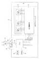
図1A,1Bは、この発明の一実施形態にかかる画像形成装置に備えられている感光体ドラム12とLEDプリントヘッド5との配置関係を示す図解図である。図1A,1Bに示すように、感光体ドラム12は、軸方向に長手の筒状体であり、その表面に感光体層が備えられている。感光体ドラム12はその表面の感光体層が図示しない放電器によって所定電位に帯電される。
【0015】
LEDプリントヘッド5は、感光体ドラム12の軸方向に延び、感光体ドラム12の表面に対向している。LEDプリントヘッド5には、その長さ方向に配列された多数個のLEDが含まれている。たとえば、この画像形成装置が、日本工業規格A列3番の用紙に600dpiの解像度の画像を形成することができる場合、LEDプリントヘッド5には、7000個の直列に配列されたLEDが備えられている。そして各LEDには、それぞれ、LEDの点灯を制御するドライバが備えられていて、各LED毎に、その点灯/消灯および点灯時間が制御される。
【0016】
LEDの点灯時間が長いと、感光体ドラム12の表面は強く露光され、その露光領域に乗るトナー量が増加する。逆にLEDの点灯時間が短いと、感光体ドラム12表面の露光強度が弱く、露光領域に乗るトナー量は減少する。そして感光体ドラム12表面に乗ったトナー量の多少により、形成されるトナー画像の階調が変化する。
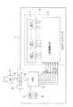
図2にLEDプリントヘッド5を有するプリンタの構成ブロック図を示す。同図で、プリンタ本体1は、CPU2、ROM3、RAM4、LEDプリントヘッド5、LED駆動手段6、LEDヘッド7、ネットワークインタフェース8、内部バス9を備えている。画像データは、たとえばネットワークケーブル10を介して接続されたパソコン11から送られてくる。
【0017】
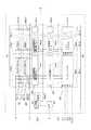
図3にLEDプリントヘッド5の構成を示す。LEDプリントヘッドは階調型であって、n(nは整数)ドットのLED(7211〜721n)が集積されたLEDアレイ71がm(mは整数)チップ並べられ、それらに対応してLEDを駆動するLED駆動回路61がmチップ並べられている。以下LEDアレイ71を駆動するLED駆動回路61の説明を行う。
例えば、4bitの階調型LEDプリントヘッドの場合、それぞれのLED駆動回路(611〜61m)は、4bit×nドット分のラッチ回路(631〜63m)、4bit×nドット分のシフトレジスタ(621〜62m)、nドット分のAND回路(6511〜65mn)をもっている。階調データはデータ線D1〜D4からシフトクロック信号線SCLKのシフトクロックに同期して1番目のLED駆動回路611に与えられる。階調データはシフトレジスタ621中を移動していき、n+1番目のデータが与えられる時、1番目に入力された階調データは2番目のLED駆動回路612のシフトレジスタ622にはいる。このように4bitの階調データがシフトレジスタ(621〜62m)中を次々に移動していきn×m組の階調データが入力されると、全てのシフトレジスタ(621〜62m)に階調データが入力されることとなる。次にラッチ信号線LAからラッチ信号が与えられ、ラッチ信号のタイミングで階調データはラッチ回路(631〜63m)にラッチされる。次にこの4bit階調データと点灯基準クロックCLK1から、点灯時間信号発生器64は各階調に応じた点灯時間信号を出力する。そしてAND回路(6511〜65mn)で点灯時間信号とストローブ信号線STからのストローブ信号とのANDがとられ、AND回路(6511〜65mn)からの出力は点灯信号としてLED(7211〜72mn)を点灯させる。Gはグランド線である。
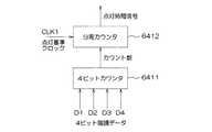
【0018】
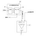
点灯時間信号発生器641は、たとえば図4のような構成をしている。すなわち、4ビットカウンタ6411と分周カウンタ6412とを有する。4ビットカウンタ6411は、データ線D1〜D4から階調データが入力されると、この値に応じて、0〜15の値(カウント数)を出力する。分周カウンタ6412には、このカウント数と、CLK1からの点灯基準クロックとが入力され、点灯基準クロックの立ち下がり回数をカウントして、入力されたカウントと同じになるまで点灯時間信号を出力する。
【0019】
たとえば図5のタイムチャートに示すように、ストローブ信号線STからのストローブ信号の立ち下がりをトリガーとして点灯時間信号を発生させる。このような点灯時間発生器64は、各LEDにつき1つづつ設けられている。
しかし、上述した制御では、階調データとLEDの点灯時間は比例関係の設定にしかできない。というのは、点灯基準クロックは一定の周波数の矩形波を用いているからであり、階調データに基づくカウントで分周しているので、カウントと点灯時間は比例関係になるからである。
【0020】
一方、電子写真方式の画像形成装置は、感光体ドラムの感度特性、現像の電位設定、転写の電位設定などにより、感光体の露光時間や露光強度と、印刷された画像濃度(ID)とは比例関係にはならない。例えば4ビット画像データをγ変換せずに階調データとして用い、印刷すると、図6に示すように、点灯時間(これと線形な比例関係にある階調データ)と印刷画像濃度とは比例せず、γ特性の関係になることが知られている。このため、階調データが小さい領域では、1つの階調データに対する印刷画像のIDの増加は小刻みで、階調データが大きい領域では、1つの階調データに対する印刷画像のIDの増加が大きくなってしまう。よって、パソコンやスキャナからの入力画像データはプリンタ部に用いる階調データに変換するときに、このプリンタエンジン部のもつγ特性に応じたγ変換用ルックアップテーブルを用いてγ変換することにより、入力画像データの値と印刷される画像のIDとが比例関係になるような処理を行う必要がある。
【0021】
【表1】
表1は、4ビットの画像データに対してγ変換を行い、4ビットの階調データを生成し、この4ビット階調データで印刷したときの画像濃度を測定したものである。こうすれば本来の画像データと印刷された画像濃度の関係は図7に示すように、ほぼ比例関係になる。しかし、LEDプリントヘッドは、有効な画像濃度領域であっても、出力できない画像濃度があるので、厳密な比例関係にならない。本来4ビットの階調データでは16階調の画像濃度が表現できなければいけないのに、ここでは実質11階調の表現しかできていない。この結果印刷される画像のIDの大きい領域を細かく表現できないという新たな問題ができる。特に中間調の領域で細かく画像濃度を表現できないと疑似輪郭が発生しやすくなるなどの問題がある。できることならばプリントヘッドに入力される階調データと印刷画像のIDとの関係は比例関係、または意図的に操作しやすいものが良い。
【0023】
そこで、この実施形態では、点灯基準クロックを以下のようにして決定することにした。
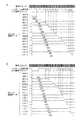
点灯基準クロック(CLK1に用いられる信号)の決定手順を図8,図9を用いて説明する。まず、本プリンタを用いて、任意の階調データでパッチを印刷し、これをスキャナで読み取り画像データを生成し、この測定データから点灯時間と印刷画像濃度との関係を求める。求めた関係が比較的線形に近い場合は図8に示すようなγ曲線(γパターンAのプリンタ)となり、また比較的γの強くでる場合は図9に示すようなγ曲線(γパターンBのプリンタ)となる。このようなγ特性は、感光体ドラムの特性および現像電位、転写電位の設定により決定されるものである。
【0024】
次に、印刷画像濃度を等間隔に分割し、この各濃度における点灯時間を求める。ここではこのプリンタの有効な最大画像濃度を1.5として、4ビットの階調データ(16階調)を用いるので、画像濃度0.1刻みで各画像濃度に対応する点灯時間を求める。
【0025】
【表2】
表2では、各濃度の点灯時間は基準クロック(CPUクロック)のパルスの数で表され、このデータは点灯基準クロックルックアップテーブルとして図2のRAM4に格納されている。
次に、この点灯基準クロックルックアップテーブルから、点灯基準クロックの波形を決定する手順を、再び図8,図9を用いて説明する。上述したように、図4に示す点灯時間信号発生器641は入力された階調データをカウントし、このカウントに応じて点灯基準クロックを分周し点灯時間信号を出力する。
【0027】
そこで、γパターンAのプリンタの場合は、階調データ0000の入力に対して、カウントは0で、点灯時間信号発生器641からの出力は無し、階調データ0001の入力に対しては、カウントは1となり、基準クロック170パルスで点灯基準クロックは1つ目の立ち下がりがあればよく、階調データ0010はカウントは2となり、基準クロック340パルスで、点灯基準クロックは2つ目の立ち下がりがあればよく、・・・階調データ1111はカウントは15となり、基準クロック1500パルスで点灯基準クロックは15番目の立ち下がりがあればよい。このようにして各カウントに対する点灯基準クロックの立ち下がりの時間を決めることにより波形は決定される。
【0028】
同様にγパターンBのプリンタの場合は、階調データ0000の入力に対して、カウントは0で、点灯時間信号発生器641からの出力は無し、階調データ0001の入力に対しては、カウントは1となり、基準クロック500パルスで点灯基準クロックは1つ目の立ち下がりがあればよく、階調データ0010はカウントは2となり、基準クロック625パルスで、点灯基準クロックは2つ目の立ち下がりがあればよく、・・・階調データ1111はカウントは15となり、基準クロック1500パルスで点灯基準クロックは15番目の立ち下がりがあればよい。このようにして点灯基準クロックの波形は決定される。
【0029】
これらの手順で求められた点灯基準クロックは、図8,図9の下に表され、それぞれのγパターンA補正用の点灯基準クロック、γパターンB補正用の点灯基準クロックの矩形波となる。
上記各γパターンの補正用の点灯基準クロックで、プリンタの各LEDを駆動した場合は、図10A,10Bに示すように、各0000〜1111の4ビット階調データに対して各々の点灯時間信号を発生する。そしてプリンタをこの点灯時間信号で動作させたときの、各0000〜1111の4ビット階調データにおける画像濃度は図11A,11Bに示すように、比例関係になり、必要な画像濃度で印刷することができる。
【0030】
上述した点灯基準クロックはγ補正用のものであるが、入力階調に対して、印刷画像濃度を操作したい時は、予め図12の(A)〜(B)の点灯基準クロックのパターンを用意しておくと良い。同図の(A)は上述したγ補正用の点灯基準クロックである。(B)〜(D)の点灯基準クロックを用いれば、同図の各々右にあるような階調データと画像濃度の関係の出力特性となる。このような複数の点灯基準クロックを生成するための複数のルックアップテーブルをRAM4に記憶させておき、ユーザーの指示により選択して用いればよい。また新たなルックアップテーブルを作成して新たな点灯基準クロックのパターンを加えても良いし、既にあるルックアップテーブルを変更して点灯基準クロックのパターンを変更することもできる。
【0031】
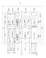
本件発明の他の実施形態にかかるプリンタの構成ブロックを図13に示す。主要な構成は図2に示す実施形態と同じなので、同一の構成には同一の符号を付す。この実施形態ではCPU2からLEDプリントヘッド5に対し、点灯基準クロックCLK1を入力せず、基準クロック信号線CLKから基準クロック(CPUクロック)を入力し、また信号線SからはこのLEDプリントヘッド5を制御する信号を入力している。
【0032】
この他の実施形態にかかるプリンタのLEDプリントヘッド5の詳細を図14に示す。主要な構成は図3に示す実施形態と同じであり、同一の構成には同一の符号を付す。この実施形態では点灯基準クロック発生器66と、LUT67が新たな構成として追加されている。LUT67には先の実施形態ではRAM4に格納されていた、画像濃度と点灯時間を基準クロックのパルス数で表したルックアップテーブルと同じものが記憶されている。点灯基準クロック発生器66には基準クロックが入力されているので、LUT67のデータとともに、図12に示すような点灯基準クロックを発生させる。ここで発生された点灯基準信号はCLK1を介して、各点灯時間信号発生器64に入力され、先の実施形態と同じように用いられる。
【0033】
このように先の実施形態ではCPU2とRAM4のルックアップテーブルを用いて発生していた点灯基準クロックをLEDプリントヘッド5自体に持たせることにより、CPUの負担を軽減することができる。またLUT67の選択、変更、新規作成も信号線Sから行うことができる。
図15は、この発明の内容を簡略化して説明するためのブロック図である。すなわちLEDプリントヘッド5に備えられた1つのLEDユニット21(1つのLEDユニット21には、1つのLEDが備えられている。)の点灯制御回路の構成を示すブロック図である。LEDユニット21には点灯要求信号(STROBE)が与えられる。また、点灯クロック発生器64から点灯基準クロックが与えられる。LEDユニット21では、点灯要求信号と点灯基準クロックとに基づいて、そのLEDの発光時間が制御される。
【0034】
点灯基準クロックは点灯時間信号発生器64から与えられる。点灯時間信号発生器64には、たとえば2GHzのCPUクロックを分周する分周回路31が備えられている。分周回路31により2GHzのCPUクロックは複数種類のクロックに分周される。そして分周されたクロックはセレクタ32へ与えられる。セレクタ32は画像データにより切換え可能になっいて、セレクタ32により選択されたクロックが点灯基準クロックとして出力される。この結果、点灯時間信号発生器64から出力される点灯基準クロックは、その周期が変更可能である。
【0035】
図16に、従来のLEDの点灯制御タイミングを参考のために示し、図17に、図15の回路によって行われるこの実施形態にかかるLEDの点灯制御タイミングを示す。図16および図17の比較から明らかなように、従来のLEDは、周期の変化しない点灯基準クロックの立ち下がりタイミングによって、点灯時間が制御される。従って、画像データの階調に対応して、LEDの点灯時間は点灯基準クロックの周期の整数倍の長さに制御されることがわかる。
【0036】
一方、この実施形態では、図17に示すように、点灯基準クロックの周期、換言すれば点灯基準クロックの立ち下がりタイミングが可変可能である。このため、画像データの階調に応じて、点灯基準クロックの立ち下がりタイミングを変化させ、LEDの点灯時間を点灯基準クロックの周期の整数倍に限定されない任意の長さに調整できることがわかる。なお、点灯基準クロックの立ち上がりタイミングに基づき点灯時間を調整することも、もちろんできる。
【0037】
次に、画像データの階調と、LEDの点灯時間と、形成されるトナー像の濃度との関係について説明をする。
図18は、理論上の画像データの階調と、点灯時間と、形成されるトナー画像の濃度との関係を示すグラフである。図18に示すように、画像データの階調、点灯時間および形成されるトナー画像の濃度IDがすべて線形な関係にあれば、点灯クロックの周期を変化させる必要はなく、画像データの階調に対応した濃度のトナー像を形成することができる。
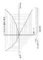
【0038】
ところが、実際には、図19に示すように、画像データの階調と、形成されるトナー像の濃度IDとは線形な関係にはなく、非線形な関係になっている。このため、画像データの階調に応じて周期が一定な点灯基準クロックにより点灯時間を制御した場合には、画像データの階調がそのまま形成されるトナー像の濃度に反映されず、たとえばトナー像の薄い部分の階調再現性が劣化するという欠点がある。
【0039】
そこで、この実施形態では、図20に示すように、点灯基準クロックの周期(換言すれば点灯基準クロックの立ち下がりタイミング)を可変することによって、画像データの階調に応じてLEDの点灯時間を点灯基準クロックの整数倍ではなく、非線形な特性で制御できるようにした。その結果、LEDの点灯により露光された領域に付着するトナー量を調整でき、形成されるトナー像の濃度を画像データの階調に線形に対応づけたものにすることができる。
【0040】
以上説明したように、この発明は、LEDプリントヘッドに含まれる各LEDの点灯時間を制御する点灯基準クロックを、その周期が変化可能なクロックとしたことにより、階調再現性の良い画像を形成できる装置を提供することができる。
この発明は、実施形態で説明したものに限定されるものではなく、請求項記載の範囲内において種々の変更が可能である。
【図面の簡単な説明】
【図1】A,Bは、この発明の一実施形態に係る画像形成装置に備えられている感光体ドラムとLEDプリントヘッドとの配置関係を示す図解図である。
【図2】LEDプリントヘッドを有するプリンタの構成ブロック図を示す。
【図3】LEDプリントヘッドの構成を示すブロック図である。
【図4】点灯時間信号発生器の構成を示すブロック図である。
【図5】従来技術の点灯時間信号発生器の動作を説明するためのタイミングチャートである。
【図6】点灯時間と印刷画像濃度とが比例せず、γ特性になることを説明するための図である。
【図7】画像データとγ変換後の画像濃度との関係を説明するための図である。
【図8】画像濃度データから点灯時間を決定する手順を説明するための図である。
【図9】画像濃度データから点灯時間を決定する手順を説明するための図である。
【図10】A,Bは、4bit階調データと点灯時間信号との関係を説明するための図である。
【図11】A,Bは、画像データと画像濃度との関係を説明するための図である。
【図12】A,B,C,Dは、各種点灯基準クロックのパターンを説明するための図である。
【図13】この発明の他の実施形態に係るプリンタの構成ブロック図である。
【図14】この発明の他の実施形態に係るプリンタのLEDプリントヘッドの詳細を示すブロック図である。
【図15】この発明の内容を簡略化して説明するためのブロック図である。
【図16】従来のLEDの点灯制御タイミングを示す参考図である。
【図17】この発明の一実施形態に係る点灯制御回路によって行われるLEDの点灯制御タイミングを示す図である。
【図18】理論上の画像データの階調と、点灯時間と、形成されるトナー画像の濃度との関係を示すグラフである。
【図19】従来の点灯制御タイミングによる画像データの階調と、点灯時間と、形成されるトナー画像の濃度との関係を示すグラフである。
【図20】この発明の一実施形態に係る点灯制御タイミングによる場合の画像データの階調と、点灯時間と、形成されるトナー画像の濃度との関係を示すグラフである。
【符号の説明】
1 プリンタ本体
2 CPU
3 ROM
4 RAM
5 LEDプリントヘッド
6 LED駆動手段
7 LEDヘッド[0001]
TECHNICAL FIELD OF THE INVENTION
The present invention relates to an image forming apparatus such as a copying machine, a facsimile machine, and a printer, and more particularly, to an image forming apparatus having an LED print head for exposing the surface of a photoconductor.
[0002]
[Prior art]
2. Description of the Related Art Among image forming apparatuses, such as copying machines and printers, which form an image by an electrophotographic method, those which form an electrostatic latent image by an LED print head are known. In such an apparatus, the LED print head has a shape facing the surface of the photosensitive drum and extending in the axial direction of the photosensitive drum. The LED print head has, for example, a configuration in which about 7,000 LEDs are arranged in a straight line.
[0003]
The lighting time of each LED of the LED print head is controlled by the lighting clock, and the lighting time is changed according to the gradation of the image data. As a result, if the lighting time is long, the surface of the photosensitive drum is strongly exposed, the amount of toner adhering to the exposed area increases, and a dark image can be formed. On the other hand, when the lighting time is short, the amount of exposure on the surface of the photosensitive drum is small, and the amount of toner on the exposed area is small, so that a thin image is formed.
[0004]
[Problems to be solved by the invention]
By the way, the lighting clock for controlling the lighting time of each LED of the conventional LED print head has a constant cycle, and the lighting time of the LED can be controlled only by an integral multiple of one cycle of the lighting clock.
However, the relationship between the lighting time of the LED, that is, the exposure time on the surface of the photosensitive drum, and the amount of toner on the exposed area is not a linear relationship but a non-linear relationship. That is, even if the exposure time is linearly increased in proportion to the gradation of the image data, the relationship between the gradation of the image data and the density of the formed toner image is linear because the development characteristics are non-linear. However, there is a problem that the gradation of the image data and the density of the formed toner image are slightly different.
[0005]
SUMMARY OF THE INVENTION The present invention has been made to solve such a problem, and an object of the present invention is to provide an image forming apparatus having an LED print head that can form an image with good gradation.
[0006]
Means for Solving the Problems and Effects of the Invention
According to the first aspect of the present invention, in an electrophotographic image forming apparatus having an LED print head in which a large number of LEDs for exposing a photoreceptor surface are arranged, a relationship between an image density and a lighting time is set in advance. A lighting time setting unitthat divides a print image density into a plurality of densities at equal intervals, and sets an LED lighting time required to form each of the divided densities in an image forming apparatus. Lighting reference clock look-up table that defines the correspondence between the number of lighting CPU clock pulses represented by the number of CPU clock pulses of the CPU, which is the control center of the CPU, and the fall time of the lighting reference clock for each count of gradation data. A gradation data counter that outputs a count number corresponding to the gradation of the input image data; A frequency dividing counter that divides a lighting reference clock and an output of the frequency dividing counter are lit until the counted number to be output is reached and the fall time determined in the lighting reference clock lookup table is reached. And an LED driving means for giving as a signal .
[0009]
According to asecond aspect of the invention, thelighting reference clock lookuptable, so that it can arbitrarily manipulate the print image density, for reproducing low image density, a large reproduction contrast, and, for high reproduced image density at least three types are provided, characterized in that it selects one, which is an image forming apparatus according to
The invention according to
Invention of
[0010]
The invention according to
[0011]
According tothis invention, because the lighting time for lighting the respective LEDs of the LED print head can be set in a non-linear, it can be a LED is lit at the optimal lighting time corresponding to the gradation of input image data . As a result, it is possible to flexibly cope with the non-linear characteristics of the gradation and the exposure time of the image data, to associate them well, and to give a formed image good gradation.
[0012]
That is, the linearity of the gradation of the image data and the image formed by the toner can be secured, and the image quality can be improved.
Further, in the image forming apparatus, the relationship between the LED lighting time and the print image density differs depending on the inherent characteristics, for example, the characteristics of the photosensitive drum, and the setting conditions, for example, the setting of the development potential and the transfer potential. Therefore, the relationship between the number of reference clocks and the gradation is prepared in a plurality of look-up tables so that any one of the look-up tables can be selected so that different relationships can be handled. preferable.
[0013]
Also, the look-up table is preferably rewritable.
According to the present invention, an image forming apparatus having good image forming performance, particularly excellent in gradation expression, can be provided by the above configuration.
[0014]
BEST MODE FOR CARRYING OUT THE INVENTION
Hereinafter, embodiments of the present invention will be specifically described with reference to the drawings.
1A and 1B are illustrative views showing an arrangement relationship between a
[0015]
The
[0016]
If the LED lighting time is long, the surface of the
FIG. 2 is a configuration block diagram of a printer having the
[0017]
FIG. 3 shows the configuration of the
For example, in the case of a 4-bit gradation type LED print head, each LED drive circuit (611-61m) has a 4-bit × n-dot latch circuit (631-63m) and a 4-bit × n-dot shift register (621-61m). 62m) and AND circuits (6511 to 65mn) for n dots. The gradation data is supplied from the data lines D1 to D4 to the first
[0018]
The lighting
[0019]
For example, as shown in the time chart of FIG. 5, the falling of the strobe signal from the strobe signal line ST is used as a trigger to generate a lighting time signal. One such
However, in the above control, the gradation data and the lighting time of the LED can only be set in a proportional relationship. This is because the lighting reference clock uses a rectangular wave having a constant frequency and is divided by the count based on the gradation data, so that the count and the lighting time are in a proportional relationship.
[0020]
On the other hand, in an electrophotographic image forming apparatus, the exposure time and exposure intensity of the photoreceptor and the printed image density (ID) are determined by the sensitivity characteristics of the photoreceptor drum, the development potential setting, and the transfer potential setting. There is no proportional relationship. For example, when 4-bit image data is used as gradation data without performing gamma conversion and printed, as shown in FIG. 6, the lighting time (gradation data having a linear proportional relationship with the lighting time) is proportional to the print image density. However, it is known that the relationship has a γ characteristic. For this reason, in a region where the gradation data is small, the increase of the print image ID for one gradation data is small, and in a region where the gradation data is large, the increase of the print image ID for one gradation data is large. Would. Therefore, when input image data from a personal computer or a scanner is converted into gradation data used in the printer unit, by performing γ conversion using a γ conversion lookup table corresponding to the γ characteristic of the printer engine unit, It is necessary to perform processing so that the value of the input image data and the ID of the image to be printed have a proportional relationship.
[0021]
[Table 1]
Table 1 shows the results of performing gamma conversion on 4-bit image data, generating 4-bit gradation data, and measuring the image density when printing with the 4-bit gradation data. In this case, the relationship between the original image data and the printed image density becomes almost proportional as shown in FIG. However, the LED print head does not have a strict proportional relationship because there is an image density that cannot be output even in an effective image density area. Originally, 4-bit grayscale data must be able to express 16 grayscale image densities, but here, only 11 grayscales can be expressed. As a result, there is a new problem that a region having a large ID of a printed image cannot be expressed in detail. In particular, if the image density cannot be expressed finely in the halftone area, there is a problem that a false contour is easily generated. If possible, the relationship between the gradation data input to the print head and the ID of the print image is preferably a proportional relationship or one that is intentionally easy to operate.
[0023]
Therefore, in this embodiment, the lighting reference clock is determined as follows.
The procedure for determining the lighting reference clock (signal used for CLK1) will be described with reference to FIGS. First, using this printer, a patch is printed with arbitrary gradation data, and this is read by a scanner to generate image data, and the relationship between the lighting time and the print image density is obtained from the measured data. When the obtained relation is relatively linear, a γ curve (printer of γ pattern A) as shown in FIG. 8 is obtained, and when the obtained γ is relatively strong, a γ curve (printer of γ pattern B) as shown in FIG. Printer). Such γ characteristics are determined by the characteristics of the photosensitive drum, the development potential, and the setting of the transfer potential.
[0024]
Next, the print image density is divided at equal intervals, and the lighting time at each density is determined. Here, since the effective maximum image density of the printer is 1.5 and 4-bit gradation data (16 gradations) is used, the lighting time corresponding to each image density is obtained in steps of 0.1 image density.
[0025]
[Table 2]
In Table 2, the lighting time of each density is represented by the number of pulses of the reference clock (CPU clock), and this data is stored in the
Next, a procedure for determining the waveform of the lighting reference clock from the lighting reference clock lookup table will be described with reference to FIGS. 8 and 9 again. As described above, the lighting
[0027]
Therefore, in the case of the printer of the γ pattern A, the count is 0 with respect to the input of the
[0028]
Similarly, in the case of the printer of the γ pattern B, the count is 0 for the input of the
[0029]
The lighting reference clocks obtained by these procedures are shown in the lower part of FIGS. 8 and 9, and are rectangular waves of the lighting reference clock for γ pattern A correction and the lighting reference clock for γ pattern B correction, respectively.
When each LED of the printer is driven by the above-mentioned lighting reference clock for correction of each γ pattern, as shown in FIGS. 10A and 10B, each lighting time signal for each of the 0000 to 1111 4-bit gradation data is output. Occurs. When the printer is operated with this lighting time signal, the image densities in the 4-bit gradation data of 0000 to 1111 are in a proportional relationship as shown in FIGS. 11A and 11B, and printing is performed at a required image density. Can be.
[0030]
The above-mentioned lighting reference clock is for γ correction. However, when it is desired to operate the print image density with respect to the input gradation, the lighting reference clock patterns of FIGS. 12A and 12B are prepared in advance. Good to do. (A) of the figure is a lighting reference clock for γ correction described above. When the lighting reference clocks (B) to (D) are used, the output characteristics of the relationship between the gradation data and the image density as shown on the right of each drawing are obtained. A plurality of look-up tables for generating such a plurality of lighting reference clocks may be stored in the
[0031]
FIG. 13 shows a configuration block diagram of a printer according to another embodiment of the present invention. Since the main configuration is the same as that of the embodiment shown in FIG. 2, the same components are denoted by the same reference numerals. In this embodiment, the lighting reference clock CLK1 is not input from the
[0032]
FIG. 14 shows details of an
[0033]
As described above, by giving the
FIG. 15 is a block diagram for simplifying and explaining the contents of the present invention. That is, it is a block diagram illustrating a configuration of a lighting control circuit of one
[0034]
The lighting reference clock is provided from the lighting
[0035]
FIG. 16 shows a conventional LED lighting control timing, and FIG. 17 shows an LED lighting control timing according to this embodiment performed by the circuit of FIG. As is clear from the comparison between FIG. 16 and FIG. 17, the lighting time of the conventional LED is controlled by the falling timing of the lighting reference clock whose period does not change. Therefore, it can be seen that the lighting time of the LED is controlled to a length that is an integral multiple of the cycle of the lighting reference clock in accordance with the gradation of the image data.
[0036]
On the other hand, in this embodiment, as shown in FIG. 17, the cycle of the lighting reference clock, in other words, the fall timing of the lighting reference clock can be changed. Therefore, it can be seen that the fall timing of the lighting reference clock can be changed according to the gradation of the image data, and the lighting time of the LED can be adjusted to an arbitrary length that is not limited to an integral multiple of the cycle of the lighting reference clock. The lighting time can of course be adjusted based on the rising timing of the lighting reference clock.
[0037]
Next, the relationship among the gradation of the image data, the lighting time of the LED, and the density of the toner image to be formed will be described.
FIG. 18 is a graph showing the relationship between the theoretical gradation of image data, the lighting time, and the density of the formed toner image. As shown in FIG. 18, if the gradation of the image data, the lighting time, and the density ID of the toner image to be formed are all in a linear relationship, it is not necessary to change the cycle of the lighting clock. A toner image having a corresponding density can be formed.
[0038]
However, actually, as shown in FIG. 19, the gradation of the image data and the density ID of the toner image to be formed do not have a linear relationship but have a non-linear relationship. For this reason, when the lighting time is controlled by a lighting reference clock whose cycle is constant in accordance with the gradation of the image data, the gradation of the image data is not reflected on the density of the toner image formed as it is, for example, There is a disadvantage that the gradation reproducibility of a thin portion is deteriorated.
[0039]
Therefore, in this embodiment, as shown in FIG. 20, by changing the cycle of the lighting reference clock (in other words, the falling timing of the lighting reference clock), the lighting time of the LED can be changed according to the gradation of the image data. Control is now possible with non-linear characteristics rather than integral multiples of the lighting reference clock. As a result, the amount of toner adhering to the area exposed by the lighting of the LED can be adjusted, and the density of the formed toner image can be linearly associated with the gradation of the image data.
[0040]
As described above, the present invention forms an image with good tone reproducibility by using a lighting reference clock that controls the lighting time of each LED included in the LED print head as a clock whose cycle can be changed. A device capable of providing the same can be provided.
The present invention is not limited to what has been described in the embodiment, and various changes can be made within the scope of the claims.
[Brief description of the drawings]
FIGS. 1A and 1B are illustrative views showing an arrangement relationship between a photosensitive drum and an LED print head provided in an image forming apparatus according to an embodiment of the present invention.
FIG. 2 is a block diagram showing a configuration of a printer having an LED print head.
FIG. 3 is a block diagram illustrating a configuration of an LED print head.
FIG. 4 is a block diagram showing a configuration of a lighting time signal generator.
FIG. 5 is a timing chart for explaining the operation of the lighting time signal generator according to the related art.
FIG. 6 is a diagram for explaining that the lighting time and the print image density are not proportional and have a γ characteristic.
FIG. 7 is a diagram for explaining a relationship between image data and image density after γ conversion.
FIG. 8 is a diagram for explaining a procedure for determining a lighting time from image density data.
FIG. 9 is a diagram illustrating a procedure for determining a lighting time from image density data.
FIGS. 10A and 10B are diagrams for explaining the relationship between 4-bit gradation data and a lighting time signal.
FIGS. 11A and 11B are diagrams for explaining the relationship between image data and image density. FIGS.
12A, 12B, 12C, and 12D are diagrams for explaining patterns of various lighting reference clocks.
FIG. 13 is a configuration block diagram of a printer according to another embodiment of the present invention.
FIG. 14 is a block diagram showing details of an LED print head of a printer according to another embodiment of the present invention.
FIG. 15 is a block diagram for simply describing the contents of the present invention.
FIG. 16 is a reference diagram showing a conventional LED lighting control timing.
FIG. 17 is a diagram showing lighting control timings of LEDs performed by the lighting control circuit according to the embodiment of the present invention.
FIG. 18 is a graph showing a relationship between a theoretical gradation of image data, a lighting time, and a density of a toner image to be formed.
FIG. 19 is a graph showing a relationship between a gradation of image data, a lighting time, and a density of a toner image to be formed by a conventional lighting control timing.
FIG. 20 is a graph showing a relationship between a gradation of image data, a lighting time, and a density of a toner image to be formed in the case of lighting control timing according to an embodiment of the present invention.
[Explanation of symbols]
1
3 ROM
4 RAM
5
Claims (5)
Translated fromJapanese画像濃度と点灯時間との関係が予め設定された点灯時間設定手段であって、
当該点灯時間設定手段は、
印刷画像濃度を等間隔に複数の濃度に分割し、分割された各濃度を形成するために必要なLEDの点灯時間を、画像形成装置の制御中枢であるCPUのCPUクロックのパルス数で表わした点灯時間CPUクロックパルス数と、階調データの各カウントに対する点灯基準クロックの立ち下がり時間との対応関係を定めた点灯基準クロックルックアップテーブルを有し、
さらに、
入力される画像データの階調に応じたカウント数を出力する階調データカウンタと、
前記階調データカウンタから出力されるカウント数になるまで、かつ、前記点灯基準クロックルックアップテーブルに定められた立ち下がり時間になるように、点灯基準クロックを分周する分周カウンタと、
前記分周カウンタの出力を点灯信号として与えるLED駆動手段と、
を有することを特徴とする画像形成装置。In an electrophotographic image forming apparatus having an LED print head in which a large number of LEDs for exposing a photoreceptor surface are arranged,
Lighting time setting meansin which the relationship between image density and lighting time is set in advance,
The lighting time setting means,
The print image density is divided into a plurality of densities at equal intervals, and the lighting time of the LED required to form each of the divided densities is represented by the number of CPU clock pulses of the CPU which is the control center of the image forming apparatus. A lighting reference clock lookup table that defines the correspondence between the lighting time CPU clock pulse number and the falling time of the lighting reference clock for each count of gradation data;
further,
A gradation data counter that outputs a count number according to the gradation of input image data;
A frequency dividing counter that divides the lighting reference clock until the count number output from the gradation data counter is reached, and so that the falling time determined in the lighting reference clock lookup table is reached;
LED driving means for providing an output of the frequency division counter as a lighting signal;
An image forming apparatus comprising:
Priority Applications (1)
| Application Number | Priority Date | Filing Date | Title |
|---|---|---|---|
| JP2001359746AJP3561703B2 (en) | 2000-12-19 | 2001-11-26 | Image forming device |
Applications Claiming Priority (3)
| Application Number | Priority Date | Filing Date | Title |
|---|---|---|---|
| JP2000385759 | 2000-12-19 | ||
| JP2000-385759 | 2000-12-19 | ||
| JP2001359746AJP3561703B2 (en) | 2000-12-19 | 2001-11-26 | Image forming device |
Publications (2)
| Publication Number | Publication Date |
|---|---|
| JP2002248808A JP2002248808A (en) | 2002-09-03 |
| JP3561703B2true JP3561703B2 (en) | 2004-09-02 |
Family
ID=26606119
Family Applications (1)
| Application Number | Title | Priority Date | Filing Date |
|---|---|---|---|
| JP2001359746AExpired - Fee RelatedJP3561703B2 (en) | 2000-12-19 | 2001-11-26 | Image forming device |
Country Status (1)
| Country | Link |
|---|---|
| JP (1) | JP3561703B2 (en) |
Cited By (1)
| Publication number | Priority date | Publication date | Assignee | Title |
|---|---|---|---|---|
| JP2006068997A (en)* | 2004-09-01 | 2006-03-16 | Fuji Xerox Co Ltd | Image forming apparatus |
Families Citing this family (1)
| Publication number | Priority date | Publication date | Assignee | Title |
|---|---|---|---|---|
| US6965393B2 (en) | 2002-11-11 | 2005-11-15 | Kyocera Mita Corporation | Image forming apparatus |
- 2001
- 2001-11-26JPJP2001359746Apatent/JP3561703B2/ennot_activeExpired - Fee Related
Cited By (1)
| Publication number | Priority date | Publication date | Assignee | Title |
|---|---|---|---|---|
| JP2006068997A (en)* | 2004-09-01 | 2006-03-16 | Fuji Xerox Co Ltd | Image forming apparatus |
Also Published As
| Publication number | Publication date |
|---|---|
| JP2002248808A (en) | 2002-09-03 |
Similar Documents
| Publication | Publication Date | Title |
|---|---|---|
| US6088050A (en) | Non-impact recording apparatus operable under variable recording conditions | |
| US5455681A (en) | Low resolution grey level printing method from high resolution binary input file | |
| EP0515162B1 (en) | Image processing method and apparatus | |
| US5809216A (en) | Method and apparatus for multiple address recording with brightness and exposure time control | |
| JPH08163363A (en) | Image forming device | |
| JP3561703B2 (en) | Image forming device | |
| US5450212A (en) | Image forming apparatus and method | |
| US5801838A (en) | Method and device to improve print quality of gray scales and color for printers | |
| US6992792B2 (en) | Digital pulse width modulator for use in electrostatic printing mechanisms | |
| US6693659B2 (en) | Image forming apparatus with a print head having variable lighting period | |
| JP2007137064A (en) | System and method for controlling image quality in digital image forming system | |
| EP0361857B1 (en) | Recording apparatus | |
| US6795100B1 (en) | Method and apparatus for controlling a light signal in electrophotographic developing type printer | |
| JP2874938B2 (en) | Optical printer device | |
| JP2810365B2 (en) | Image forming device | |
| US5126758A (en) | Optical printer | |
| JP3325298B2 (en) | Recording device | |
| JP2632826B2 (en) | Image forming device | |
| JP3062201B2 (en) | Image forming device | |
| KR101079573B1 (en) | Pulse modulation-type image forming apparatus with high resolution | |
| JP3190269B2 (en) | Image processing method | |
| JPH03101366A (en) | How to drive the line head | |
| JPH04286463A (en) | Halftone printer and display device | |
| JPH09191407A (en) | Image forming apparatus and method | |
| JPH01113246A (en) | color image forming device |
Legal Events
| Date | Code | Title | Description |
|---|---|---|---|
| A131 | Notification of reasons for refusal | Free format text:JAPANESE INTERMEDIATE CODE: A131 Effective date:20040203 | |
| A521 | Written amendment | Free format text:JAPANESE INTERMEDIATE CODE: A523 Effective date:20040325 | |
| TRDD | Decision of grant or rejection written | ||
| A01 | Written decision to grant a patent or to grant a registration (utility model) | Free format text:JAPANESE INTERMEDIATE CODE: A01 Effective date:20040512 | |
| A61 | First payment of annual fees (during grant procedure) | Free format text:JAPANESE INTERMEDIATE CODE: A61 Effective date:20040531 | |
| R150 | Certificate of patent (=grant) or registration of utility model | Free format text:JAPANESE INTERMEDIATE CODE: R150 | |
| FPAY | Renewal fee payment (prs date is renewal date of database) | Free format text:PAYMENT UNTIL: 20100604 Year of fee payment:6 | |
| FPAY | Renewal fee payment (prs date is renewal date of database) | Free format text:PAYMENT UNTIL: 20110604 Year of fee payment:7 | |
| FPAY | Renewal fee payment (prs date is renewal date of database) | Free format text:PAYMENT UNTIL: 20110604 Year of fee payment:7 | |
| FPAY | Renewal fee payment (prs date is renewal date of database) | Free format text:PAYMENT UNTIL: 20120604 Year of fee payment:8 | |
| FPAY | Renewal fee payment (prs date is renewal date of database) | Free format text:PAYMENT UNTIL: 20120604 Year of fee payment:8 | |
| S533 | Written request for registration of change of name | Free format text:JAPANESE INTERMEDIATE CODE: R313533 | |
| R350 | Written notification of registration of transfer | Free format text:JAPANESE INTERMEDIATE CODE: R350 | |
| FPAY | Renewal fee payment (prs date is renewal date of database) | Free format text:PAYMENT UNTIL: 20120604 Year of fee payment:8 | |
| FPAY | Renewal fee payment (prs date is renewal date of database) | Free format text:PAYMENT UNTIL: 20130604 Year of fee payment:9 | |
| FPAY | Renewal fee payment (prs date is renewal date of database) | Free format text:PAYMENT UNTIL: 20140604 Year of fee payment:10 | |
| LAPS | Cancellation because of no payment of annual fees |