JP3559754B2 - Fingerprint authentication device - Google Patents
Fingerprint authentication deviceDownload PDFInfo
- Publication number
- JP3559754B2 JP3559754B2JP2000223345AJP2000223345AJP3559754B2JP 3559754 B2JP3559754 B2JP 3559754B2JP 2000223345 AJP2000223345 AJP 2000223345AJP 2000223345 AJP2000223345 AJP 2000223345AJP 3559754 B2JP3559754 B2JP 3559754B2
- Authority
- JP
- Japan
- Prior art keywords
- fingerprint
- image sensor
- optical image
- infrared
- sensitivity
- Prior art date
- Legal status (The legal status is an assumption and is not a legal conclusion. Google has not performed a legal analysis and makes no representation as to the accuracy of the status listed.)
- Expired - Fee Related
Links
Images


Classifications
- G—PHYSICS
- G06—COMPUTING OR CALCULATING; COUNTING
- G06V—IMAGE OR VIDEO RECOGNITION OR UNDERSTANDING
- G06V40/00—Recognition of biometric, human-related or animal-related patterns in image or video data
- G06V40/10—Human or animal bodies, e.g. vehicle occupants or pedestrians; Body parts, e.g. hands
- G06V40/12—Fingerprints or palmprints
- G06V40/1382—Detecting the live character of the finger, i.e. distinguishing from a fake or cadaver finger
- G06V40/1394—Detecting the live character of the finger, i.e. distinguishing from a fake or cadaver finger using acquisition arrangements
- G—PHYSICS
- G06—COMPUTING OR CALCULATING; COUNTING
- G06V—IMAGE OR VIDEO RECOGNITION OR UNDERSTANDING
- G06V40/00—Recognition of biometric, human-related or animal-related patterns in image or video data
- G06V40/40—Spoof detection, e.g. liveness detection
Landscapes
- Engineering & Computer Science (AREA)
- Human Computer Interaction (AREA)
- Physics & Mathematics (AREA)
- General Physics & Mathematics (AREA)
- Multimedia (AREA)
- Theoretical Computer Science (AREA)
- Image Input (AREA)
- Measurement Of The Respiration, Hearing Ability, Form, And Blood Characteristics Of Living Organisms (AREA)
Description
Translated fromJapanese【0001】
【発明の属する技術分野】
本発明は光学式の指紋認証装置に関する。
【0002】
【従来の技術】
高度に情報化してきた現代社会において個人認証は火急の課題である。情報化による利便性と引き換えに、プライバシ情報の漏洩や機密組織への不正侵入の危険性が伴うこととなったからである。その対策として、例えば、銀行でキャッシュカードを使用するときには暗証番号を入力し、コンピュータルームへ入室するときには資格証明カードを読み込ませてパスワードを入力することを義務付けたりしている。しかし、今日はカード万能時代とも称されるように個人が所有するカードは非常に多くなっており、その管理が厄介である。また暗証番号やパスワードを忘れたり、他人に漏洩ないしは解読される虞もある。
【0003】
暗証番号やパスワードに代わる有力な個人認証の手段として指紋を用いることが古くから知られている。指紋は人体に備わった高度な識別情報となり得て、当然ながら本人が記憶する必要がない。一般的な指紋照合装置は、イメージセンサに指紋が入力されると、認識部で指紋の画像処理を行い、マニューシャと称される指紋の特徴点を検出する。さらに、入力された指紋と予め登録されたデータベース上の指紋との類似度をマニューシャから算出する。この類似度はスコアと呼ばれる数値で表され、スコアが高いほど、入力された指紋とデータベース上の指紋との類似度が高いとされる。そして、スコアが一定の閾値を超えた場合、入力された指紋とデータベースに登録されている指紋が同一であると認識する。
【0004】
しかし、このような指紋認証装置では、生体の指紋とレプリカ(非生体で作成した指紋の模造品の意)を区別することができない。このため、例えば生体の指紋を精巧に撮った写真が入力されても、生体の指紋と認識される虞がある。
【0005】
従来から、このような弊害を回避するために様々な提案がされてきている。例えば、特許番号第2554667号の「個人認証装置」(従来例1)は、認証を行なうために用いる身体部位の温度を計測する手段(具体的には指紋読み取り部に配置された熱電対)と、計測した温度が予め設定された体温近接の温度範囲(摂氏30〜38度)の温度内か否かを判定する手段と、判定の結果、予め設定された温度範囲内の場合に始めて認証の照合を行う手段とを具備する。この技術によれば、被認証権保持者の身体部位以外、例えば写真や切り取られた指は認証しない個人認証装置が得られるとしている。なお、本装置は、指を指紋読み取り部に接触させて指紋を読み取る接触式方法を採用している。
【0006】
また、特開平11−235452号公報に記載の「識別機能付施錠開放装置」(従来例2)には、遊技場のセキュリティ対策の手段として光学式の指紋照合装置を用いることが記載されている。光学式の指紋照合装置は、プリズムに当接している指の指紋部分に照明光を照射し、その反射光をイメージセンサに導いて指紋パターンを検出する構成を採用する。この装置は、予め登録されている指紋データとプリズムに当接された指紋のパターンとを照合する指紋照合手段と、指の識別を行なう指識別手段と、指紋照合手段による照合が一致し且つ指識別手段によって指の識別が行なわれたとき、施錠装置の解錠を行なう解錠制御手段とを具備する。そして、指識別手段は、体温,脈,爪と皮膚,指の形状であってよいとする。
【0007】
更に、特開平10−18795号公報に記載の「一体型の加熱用抵抗器を備えた指紋読取りシステム」(従来例3)は、上述の接触式が、指紋を読み取る手段と身体部位の温度を計測する手段とが分離されているのに対して、両者を一体化したものである。すなわち、指紋を読み取る指を押しつけるセンサは、温度変化に敏感なエレメントの活性表面、および感受エレメントの温度の過渡的な変化を生み出す一体型の加熱用抵抗器を有する。加熱用抵抗器による熱変化が、感受エレメントのマトリックスと接触する指紋の線の溝と隆起の間の熱伝導の差によって異なる電気信号を与える。これに基づいて指紋認識を行うと共に、指紋の読取り中に、その指が放出する固有の熱を介して、それが実際に生きている個人の一部であることを認識することを可能としたものである。
【0008】
【発明が解決しようとする課題】
しかしながら、上述の従来例1では、熱電対で被測定物の温度を検出し、それが所定範囲(30〜38℃)ならば人体である、と見なしているので、レプリカを所定温度に暖めておけば、人体であると誤認してしまい問題解決になっていない。
【0009】
また、従来例2では、非接触式でイメージセンサ106で指紋パターンを認識し、一方、検出器101で体温や脈拍等を検出している。体温検出の場合は、従来例1と同様にレプリカを暖めておけばごまかせる。また、脈拍検出の場合は、指先の脈拍を測るとなると相当高感度のセンサが必要で非現実的であり、仮にできたとしても脇役の検出器の方が主役のイメージセンサより遥かに高価になっていしまい、この点からも非現実的である。
【0010】
更に、従来例3は、指紋読取り部と体温検出器が一体となったものであるが、指紋を読み取るセンサ自体が温度変化に敏感なエレメントを用いているので、周囲温度の影響を受け易く、従って、夏や冬などでセンサの閾値を変更しなければならない、というメンテナンスの問題が起こる。
【0011】
本発明は、以上の問題点を解消するためになされたものであって、その第1の目的は、周囲温度による影響が少なく安定した指紋認証を提供することにある。
【0012】
本発明の第2の目的は、メンテナンスフリーの指紋認証装置を提供することにある。
【0014】
【課題を解決するための手段】
本発明の指紋認証装置は、赤外領域に感度を有する第1の光学イメージセンサと可視光領域に感度を有する第2の光学イメージセンサとを隣り合わせて配置した光学イメージセンサで指紋認証対象物を撮像する撮像部と、前記撮像部から得られたデータを画像処理して指紋画像を得る画像処理部と、前記指紋画像を予め登録されている指紋データと照合する照合部を備えていることを特徴とする。
【0015】
具体的には、本発明の光学イメージセンサはCCDまたはCMOSであり、また、本発明における赤外感度を持つ光学イメージセンサまたは前記赤外感度を持つブロックは、P型サブストレイトとN型チャネル層の間に、通常のPウェルよりも濃度が薄くて、深く形成されたディープPウエル構造がN型チャネル層の直下に形成されることを特徴とする。
【0016】
【発明の実施の形態】
本願発明は、被写体(指)からの散乱光もしくは反射光を赤外光に感度を有する光学イメージセンサを使用して被写体撮像し、これによって被写体の画像(指紋画像)を得るとともに、その鮮明度を判定して、その被写体が生体(人体)か、または非生体(レプリカ)かを判定する。その結果、生体と判定したら、得られた画像と予め登録されている画像を比較し、一致したら本人であると判定する。
【0017】
本願発明は、赤外光に感度を有する2次元の光学イメージセンサにCCDまたはCMOSを使用し、被写体に赤外光を照射してその像を撮像したところ、生体では鮮明な指紋の像が得られ、一方、レプリカでは鮮明な像が得られなかった、という実験結果に基づいたものである。ここで、レプリカの材料として、ゴムやプラスチックや石膏などを使用した。これらの材料を使用した理由は、指紋などのレプリカを作る場合は、先ず指の型をとって、これに材料を流し込んで造るのが最も簡便で造り易いと考えたためである。なお、上記現象の理由は、現時点では解明されていないが、再現性のある実験結果が得られている。
【0018】
初めに、赤外領域に感度を有する光学イメージセンサを使用した指紋認識装置について図面を参照して説明する。
【0019】
図1は、赤外領域に感度を有する光学イメージセンサを使用した指紋認証装置の第1の例を示す構成図である。この例は、プリズム18およびレンズ19を使用する光学式の指紋認証装置であり、赤外光源12および赤外感度を持つ光学イメージセンサ13を採用している。
【0021】
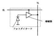
ここで、赤外感度を持つ光学イメージセンサ13について説明する。赤外感度を持つ光学イメージセンサとは、赤外光に対して感応するイメージセンサをいい、生体に対しては鮮明な画像を生成するが、レプリカに対しては不鮮明な画像を生成する性質を有する。一般に、光学イメージセンサは、周知のように、図7に示すフォトダイオードと増幅器から成る多数のエレメントをマトリックス状に配置したものである。すなわち、光源からの光がフォトダイオードに入射されると、入射光に比例した電流がフォトダイオードで発生する。この電流を増幅器で増幅し、取り出すことにより、光に対する電気信号が得られる。このように作動するエレメントからマトリックスを形成するには、増幅器の活性化端子をマトリックスの水平線HL、増幅器の出力をマトリックスの垂直線VLに接続する。
【0022】
図6(A)は赤外感度を持たない光学イメージセンサ、図6(B)は赤外感度を持つ光学イメージセンサ13のエレメントの半導体デバイス構造を示す断面図である。赤外感度を持たない光学イメージセンサでは、図6(A)に示すように、フォトダイオードを構成するP型サブストレイト(P−substrate)とN型チャネル層(N)の間には層の浅いP型ウエル(P−well)が存在するだけである。
【0023】
これに対して、赤外感度を持つ光学イメージセンサ13では、図6(B)に示すように、P型サブストレイト(P−substrate)とN型チャネル層(N)の間に、ディープPウエル(Deep P−Well)構造が形成される。ディープPウエルとは、通常のPウエルより濃度が薄くて、層が深く形成されたPウエル構造をいい、N型チャネル層の直下に形成される。この結果、通常のPウエルはN型チャネル層の直下の両端側にディープPウエルの上にのみ形成されることになる。
【0024】
赤外光は、可視光よりも半導体デバイスの深い所で電荷を発生するため、ディープPウエル構造によって、この深い所で発生する電荷を補足することが可能になる。したがって、ディープPウエル構造を有する光学イメージセンサ13は、赤外感度を持つことになるのである。上記ではCCDイメージセンサを例に説明したが、CMOSイメージセンサでもよいことは明かである。
【0025】
次に、第1の例(図1)の動作について、図8に示すフローチャートを参照して説明する。
【0026】
指紋認証を行うときには、先ず、制御部11は上位装置(図示せず)からの指示により、赤外光源12から赤外光をプリズム18に向けて照射する。このとき、プリズム18上には、指紋認証の対象物(正規の場合は人体の指10)が置かれている。プリズム18に入射された赤外光は、指10とプリズム表面との接触面で反射され、レンズ19で集光されて光学イメージセンサ13に入力する。光学イメージセンサ13は、入射されてきた赤外光を電流信号に変換し画像処理部14に入力する。
【0027】
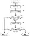
画像処理部14は、光学イメージセンサ13から入力した電流について、制御部11からの制御により画像処理を行う(図8のステップS1)。このとき、上述のような赤外光の性質により、指10で反射された赤外光からは鮮明な指紋の画像が得られるが、もしもレプリカがプリズム18上に置かれている場合には、不鮮明な画像となる。画像処理部14は得られた画像からマニューシャを検出し(図8のステップS2)、そのマニューシャ数が一定以上か否を判定する(図8のステップS3)。その結果により、マニューシャ数が一定以下の場合には、認証不可とする。
【0028】
一方、マニューシャ数が一定以上の場合には、照合部15において、指紋照合処理が行われる(図8のステップS4)。指紋照合処理においては、入力された指紋と予め登録された指紋データベース16上の指紋と画像データと指紋データベース16中の画像データと突き合わせ、それらの間の類似度をマニューシャから算出し、この類似度をスコアと呼ばれる数値で表す。そして、スコアが閾値以上か否かを判定する(図8のステップS5)。その結果、スコアが閾値以下なら認証不可とする。スコアが閾値以上なら正当な者の指紋であるとして認証する。
【0029】
この例は、従来の光学部品を用いた光学式指紋認証装置において、可視光源を赤外光源に、また光学イメージセンサを赤外感度を持つ光学イメージセンサにそれぞれ取り換えれば、容易に実現できるので、既存装置からの改造が容易である点に意義がある。
【0030】
図2は赤外領域に感度を有する光学イメージセンサを使用した指紋認証装置の第2の例を示す構成図である。この指紋認証装置は、プリズム,レンズ等の光学部品を使用せず、指を光学イメージセンサに直接接触させる光学式指紋認証装置に対して、第1の例(図1)と同様に、赤外光源22および赤外感度を持つ光学イメージセンサ23を採用したものである。
【0031】
すなわち、この装置では、指を光で直接照射し、その散乱光を2次元配列された多数の受光素子から成る2次元イメージセンサで受光する。指紋入力時には指紋が受光素子の受光面に近接配置される。そして、受光面が指紋稜線部と近接している受光素子により、指紋稜線部を介して指先内部からの散乱光が良好に届く明部領域を指紋稜線として検出する。また、受光面が指紋谷間部と近接している受光素子により、指先内部からの散乱光があまり届かない暗部領域を指紋谷間部として検出する。
【0032】
図2において、赤外光源22および光学イメージセンサ23は上述のように構成される。指紋照合を行うときには、光学イメージセンサ23の上に指20が直接置かれる。赤外光源22から照射された赤外光は指20で散乱し、光学イメージセンサ23に受光される。その後の処理は、第1の例(図1)における処理と同様であり、図8のフローチャートが適用される。また、図2と図1において、照番号2桁中の1桁目の数字が同じ構成要素は同じ機能を有する。
【0033】
次に、本発明の実施例について説明する。図3は本発明の指紋認証装置の第1の実施例を示す構成図である。この実施例は、プリズム38およびレンズ39を使用する光学式の指紋認証装置であり、赤外感度を持つ光学イメージセンサ33を採用する点は、図1に示した第1の例と共通する。しかし、可視光および赤外光が混じった光を照射する可視・赤外光源32を使用し、光学イメージセンサ33に工夫がされており、それに伴って、リファレンス処理部37が設けられていることを特徴とする。
【0034】
光学イメージセンサ33は、赤外感度を持つブロックと赤外感度を持たないブロックから構成される。前者は図6(B)、後者は図6(A)のように半導体デバイスを構成するのである。このブロック分けは、光学イメージセンサ33が1チップで構成される場合には、1チップに両ブロックを混在させる。また、光学イメージセンサ33を赤外感度を持つチップと、赤外感度を持たないチップで構成してもよい。この方法によればチップの歩留まりが向上する。更に、簡易な方法としては、赤外感度を持つ光学イメージセンサに赤外カットフィルタを部分的に貼ることにより、その部分を赤外感度を持たないブロックとすることもできる。
【0035】
図5は、光学イメージセンサ33における生体とレプリカの判別を説明するための図であり、図5の上半分が赤外感度を持つブロック、下半分が赤外感度を持たないブロックを表している。図5(A)に示すように、指紋認証対象の指を光学イメージセンサ33に置いた場合、その指が生体のものであれば、光学イメージセンサ33から得られる画像は、図5(B)に示すように、光学イメージセンサ33の上半分は赤外感度を持つため鮮明な指紋画像となり、また下半分は赤外感度を持たないが可視光感度は持つため鮮明な指紋画像となる。
【0036】
一方、指がレプリカであれば、光学イメージセンサ33から得られる画像は、図5(C)に示すように、光学イメージセンサ33の上半分は赤外感度を持つため不鮮明な指紋画像となり、また下半分は赤外感度を持たないが可視光感度は持つため鮮明な指紋画像となる。
【0037】
リファレンス処理部37は、光学イメージセンサ33内の赤外感度を持つブロックと赤外感度を持たないブロックの間の入力指紋画像の鮮明度を比較する。図5から明らかなように、生体の指であればブロック間で鮮明度に差がないが、レプリカの指であればブロック間で鮮明度に差がある。このことによって、指が生体のものか否かを判別できる。
【0038】
なお、図5は説明を単純化するために、光学イメージセンサ33を2つのブロックに分けた例を示したが、もっと多くのブロックに分割してもよい。その場合、赤外感度を持つブロックと赤外感度を持たないブロックを市松模様のように配置してもよい。細かく分割すればするほど、リファレンス処理部37における比較の対象となる指紋画像の部分が接近するので、更に正確な比較ができるようになる。光学イメージセンサ33の1行ごとに、赤外感度を持つブロックと赤外感度を持たないブロックを配置するのが理想である。また、ブロック分けも、図5に示したように横方向ではなく、縦方向にしてもよい。
【0039】
図9は第1の実施例(図3)で使用する処理フローチャートであり、図8のステップS1の前に、「鮮明度の差は一定範囲か」をチェックするステップT1が追加された形になっており、ステップT1で肯定された場合にステップT2以下の処理対象となる。図9のステップT2〜T6は図8のステップS1〜S5に対応する。
【0040】
リファレンス処理部37におけるブロックの画像比較の具体的な方法としては、次の方法が考えられる。このような方法は、リファレンス処理部37における例えばDSP(Digital Signal Processor)により行われる。
【0041】
画像比較の具体的な方法の第1は、入力する指紋画像についてブロックそれぞれの鮮明度のフーリエ変換をする方法である。この場合のフーリエ変換では、指紋画像の明部領域と暗部領域の遷移密度を空間周波数に変換し、遷移密度が高い部分は空間周波数が高く、遷移密度が低い部分は空間周波数が低くなる。生体の場合は、赤外感度を持つブロックと赤外感度を持たないブロックの両方とも鮮明画像が得られるため、図5(B)に示すように、両ブロックとも空間周波数が高く、空間周波数に差がない。一方、レプリカの場合には、図5(C)に示すように、赤外感度を持つブロックでは不鮮明画像となるため空間周波数は低く、赤外感度を持たないブロックでは鮮明画像が得られるため空間周波数は高く、両ブロック間で空間周波数に差が出ることになる。このことを利用してレプリカを排除するのである。
【0042】
画像比較の具体的な方法の第2は、入力する指紋画像についてブロックそれぞれの鮮明度の標準偏差を計算する方法である。レプリカを撮影した場合には、赤外感度を持つブロックの画像は不鮮明なため、赤外感度を持たないブロックの画像よりも鮮明度の標準偏差が低い。生体の場合は、ブロックの間で標準偏差に差がないが、レプリカの場合には、赤外感度を持つブロックの標準偏差が、赤外感度を持たないブロックに比べて低くなる。このことを利用してレプリカを排除するのである。
【0043】
なお、赤外感度を持つブロックと赤外感度を持たないブロックとでは、感度の絶対値に差が生じる。そこで、制御部31は、それぞれのブロックについて、シャッタースピードを独立に設定することにより適切な画像を得るようにすることができる。ここで、シャッタースピードとは、光学イメージセンサ33におけるPN接合部において、N型チャネル層にリセットをかけて電流信号の読出しを開始してから終了するまでの時間をいい、感度の高い赤外感度を持つブロックのシャッタースピードは赤外感度を持たないブロックのシャッタースピードより速く設定する。この結果、前者の露光時間は後者の露光時間より短くなるので、感度の差を補填し、全体として両ブロックとも同じ明るさの画像が得られるようにするのである。
【0044】
また、制御部31は、それぞれのブロックについて、適切なセンサ感度を独立に設定するようにしても同様な効果を得ることができる。具体的には、光学イメージセンサ33におけるアンプの電流増幅率を、赤外感度持つブロックに対しては、赤外感度持たないブロックに対してよりも低く設定するのである。
【0045】
更に、制御部31が、上述のように、2つのブロックに対して同時に異なるシャッタースピードで動作ることが困難な場合には、制御部31は、それぞれのブロックに対する適切なシャッタースピードを検出し、時間を分けてそれぞれのシャッタースピードで撮像した後、撮像されたブロックの画像同士を合成するようにしてもよい。このことは、2つのブロックを異なる電流増幅率で動作させる場合についても同様に適用できる。
【0046】
図4は本発明の指紋認証装置の第2の実施例を示す構成図である。この実施例は、プリズム,レンズ等の光学部品を使用せず、指を光学イメージセンサに直接接触させる光学式指紋認証装置であって、第2の例(図2)が第1の例(図1)に対して持つ関係と同様な関係を第1の実施例について有する。すなわち、この指紋認証装置は、可視光および赤外光が混じった光を照射する可視・赤外光源41を使用し、光学イメージセンサ43に工夫がされており、それに伴って、リファレンス処理部47が設けられている。光学イメージセンサ43は、赤外感度を持つブロックと赤外感度を持たないブロックから構成され、リファレンス処理部47は、光学イメージセンサ43内の赤外感度を持つブロックと赤外感度を持たないブロックの間の入力指紋画像の鮮明度を比較する。
【0047】
可視・赤外光源42から照射された赤外光は指40で散乱し、光学イメージセンサ43に受光される。その後の処理は、第1の実施例(図3)おける処理と同様であり、図9のフローチャートが適用される。また、図4と図3において、参照番号2桁中の1桁目の数字が同じ構成要素は同じ機能を有する。
【0048】
【発明の効果】
本発明の第1の効果は、指紋画像の読み取りに、従来のような圧電効果および/またはパイロ電気効果を利用せず、赤外感度を有する光学イメージセンサを採用したため、周囲温度による影響が少なく安定した指紋認証装置を提供することができるということである。
【0049】
本発明の第2の効果は、周囲温度による影響が少なく安定した指紋認証を行えることから、メンテナンスを軽減した指紋認証装置を提供することができるということである。
【図面の簡単な説明】
【図1】赤外領域に感度を有する光学イメージセンサを使用した指紋照合装置の第1の例を示す構成図
【図2】赤外領域に感度を有する光学イメージセンサを使用した指紋照合装置の第2の例を示す構成図
【図3】本発明の指紋照合装置の第1の実施例を示す構成図
【図4】本発明の指紋照合装置の第2の実施例を示す構成図
【図5】本発明の第1の実施例および第2の実施例おける光学イメージセンサでの生体とレプリカの判別を説明するための模式図
【図6】赤外感度を持たない光学イメージセンサ(A)と赤外感度を持つ光学イメージ
センサ(B)の半導体デバイスの構造を示す断面図
【図7】一般的な光学イメージセンサのエレメントを示す回路図
【図8】指紋照合装置の第1の例(図1)および第2の例(図2)のフローチャート
【図9】本発明の指紋照合装置の第1の実施例(図3)および第2の実施例(図4)のフローチャート[0001]
TECHNICAL FIELD OF THE INVENTION
The present invention relates to an optical fingerprint authentication device.
[0002]
[Prior art]
Personal authentication is an urgent issue in today's highly computerized society. This is because, in exchange for the convenience provided by computerization, there is a risk of privacy information leaking and unauthorized intrusion into confidential organizations. As a countermeasure, for example, when a bank card is used at a bank, a password must be entered, and when entering a computer room, a credential card must be read and a password must be entered. However, the number of personally owned cards is so large that it is called the universal era of cards today, and the management of such cards is troublesome. There is also a risk that the password or password may be forgotten, leaked or decoded by others.
[0003]
It has long been known to use fingerprints as a powerful means of personal authentication in place of passwords and passwords. Fingerprints can be sophisticated identification information of the human body and need not be memorized by the person. In a general fingerprint collation device, when a fingerprint is input to an image sensor, the recognition unit performs fingerprint image processing to detect a feature point of the fingerprint called a minutiae. Further, the similarity between the input fingerprint and the fingerprint on the database registered in advance is calculated from the minutiae. This similarity is represented by a numerical value called a score, and the higher the score, the higher the similarity between the input fingerprint and the fingerprint on the database. Then, when the score exceeds a certain threshold value, it is recognized that the inputted fingerprint and the fingerprint registered in the database are the same.
[0004]
However, such a fingerprint authentication device cannot distinguish between a fingerprint of a living body and a replica (a replica of a fingerprint created in a non-living body). For this reason, for example, even if a photograph in which a fingerprint of a living body is finely taken is input, there is a possibility that the fingerprint is recognized as a living body fingerprint.
[0005]
Conventionally, various proposals have been made to avoid such adverse effects. For example, a "personal authentication device" of Patent No. 25554667 (conventional example 1) includes a unit for measuring the temperature of a body part used for performing authentication (specifically, a thermocouple disposed in a fingerprint reading unit). Means for judging whether or not the measured temperature is within a predetermined temperature range close to the body temperature (30 to 38 degrees Celsius); Means for performing collation. According to this technology, a personal authentication device that does not authenticate a part other than the body part of the person to be authenticated, for example, a photograph or a cut-out finger, is obtained. Note that the present device employs a contact method in which a finger is brought into contact with a fingerprint reading unit to read a fingerprint.
[0006]
Japanese Patent Application Laid-Open No. 11-235452 discloses a "locking / unlocking device with an identification function" (conventional example 2) in which an optical fingerprint collation device is used as a security measure in a game arcade. . The optical fingerprint collation device employs a configuration in which a fingerprint portion of a finger in contact with a prism is irradiated with illumination light, and the reflected light is guided to an image sensor to detect a fingerprint pattern. This apparatus includes a fingerprint collating unit for collating fingerprint data registered in advance with a pattern of a fingerprint abutted on a prism, a finger identifying unit for identifying a finger, and a fingerprint matching unit that matches the fingerprints. An unlock control means for unlocking the locking device when a finger is identified by the identification means. The finger identification means may be in the form of body temperature, pulse, nail and skin, and finger shape.
[0007]
Further, in the "fingerprint reading system having an integrated heating resistor" (conventional example 3) described in Japanese Patent Application Laid-Open No. H10-18795, the contact type described above uses a fingerprint reading means and a body part temperature. While the means for measuring is separated, both are integrated. That is, a finger pressing sensor that reads a fingerprint has an active surface of the element that is sensitive to temperature changes and an integrated heating resistor that produces a transient change in the temperature of the sensing element. The heat change by the heating resistor gives a different electrical signal due to the difference in heat conduction between the groove and the ridge of the fingerprint line in contact with the matrix of the sensitive element. Based on this, it was possible to perform fingerprint recognition, and during the reading of the fingerprint, through the inherent heat emitted by the finger, it was possible to recognize that it was actually part of a living individual Things.
[0008]
[Problems to be solved by the invention]
However, in the conventional example 1 described above, the temperature of the object to be measured is detected by a thermocouple, and if the temperature is in a predetermined range (30 to 38 ° C.), it is regarded as a human body. In other words, they are mistaken for a human body and have not solved the problem.
[0009]
In the second conventional example, the fingerprint pattern is recognized by the image sensor 106 in a non-contact manner, and the body temperature, the pulse, and the like are detected by the detector 101. In the case of body temperature detection, the replica is warmed and cheated as in Conventional Example 1. In addition, in the case of pulse detection, when measuring the pulse of the fingertip, a sensor with a considerably high sensitivity is required and it is impractical, and even if it can be done, the detector of the supporting character is much more expensive than the image sensor of the main character. It is unrealistic from this point.
[0010]
Furthermore, in the conventional example 3, the fingerprint reading unit and the body temperature detector are integrated, but since the sensor for reading the fingerprint itself uses an element sensitive to a temperature change, it is easily affected by the ambient temperature, Therefore, there arises a maintenance problem that the threshold value of the sensor must be changed in summer or winter.
[0011]
The present invention has been made to solve the above problems, and a first object of the present invention is to provide a stable fingerprint authentication which is less affected by an ambient temperature.
[0012]
A second object of the present invention is to provide a maintenance-free fingerprint authentication device.
[0014]
[Means for Solving the Problems]
The fingerprint authentication device according to thepresent invention uses a first optical image sensor having sensitivity in the infrared region and a second optical image sensor having sensitivity in the visible light region adjacent to each other to identify a fingerprint authentication target with an optical image sensor. An imaging unit for imaging, an image processing unit for performing image processing on data obtained from the imaging unit to obtain a fingerprint image, and a collation unit for collating the fingerprint image with fingerprint data registered in advance. Features.
[0015]
Specifically, the optical image sensor of the present invention is a CCD or a CMOS, and the optical image sensor having infrared sensitivity or the block having infrared sensitivity of the present invention includes a P-type substrate and an N-type channel layer. The deep P-well structure having a lower concentration than the ordinary P-well and deeply formed is formed immediately below the N-type channel layer.
[0016]
BEST MODE FOR CARRYING OUT THE INVENTION
The invention of the present application captures an image of a subject using an optical image sensor having sensitivity to infrared light of scattered light or reflected light from the subject (finger), thereby obtaining an image of the subject (fingerprint image) and the sharpness of the image. To determine whether the subject is a living body (human body) or a non-living body (replica). As a result, if it is determined that the subject is a living body, the obtained image is compared with a pre-registered image.
[0017]
According to the present invention, when a CCD or CMOS is used as a two-dimensional optical image sensor having sensitivity to infrared light, a subject is irradiated with infrared light and an image thereof is taken, and a clear fingerprint image is obtained in a living body. On the other hand, it was based on the experimental result that a clear image could not be obtained with the replica. Here, rubber, plastic, gypsum, or the like was used as a material for the replica. The reason why these materials are used is that when making a replica such as a fingerprint, it is considered that it is easiest and easiest to make a finger by first taking a mold and pouring the material into the finger. The reason for the above phenomenon has not been elucidated at present, but reproducible experimental results have been obtained.
[0018]
First, a fingerprint recognition device using an optical image sensor having sensitivity in the infrared region will be described with reference to the drawings.
[0019]
FIG. 1 is a configuration diagram showing afirst example ofa fingerprint authentication deviceusing an optical image sensor having sensitivity in the infrared region .This example is an optical fingerprint authentication device using a prism 18 and a lens 19, and employs an infrared light source 12 and an optical image sensor 13 having infrared sensitivity.
[0021]
Here, the optical image sensor 13 having infrared sensitivity will be described. An optical image sensor having infrared sensitivity is an image sensor that is sensitive to infrared light, and has the property of generating a clear image for a living body but generating an unclear image for a replica. Have. Generally, as is well known, an optical image sensor is one in which a number of elements including a photodiode and an amplifier shown in FIG. 7 are arranged in a matrix. That is, when light from a light source is incident on a photodiode, a current proportional to the incident light is generated in the photodiode. By amplifying this current with an amplifier and extracting it, an electric signal for light is obtained. To form a matrix from the elements operating in this way, the activation terminals of the amplifier are connected to the horizontal line HL of the matrix and the output of the amplifier is connected to the vertical line VL of the matrix.
[0022]
FIG. 6A is an optical image sensor having no infrared sensitivity, and FIG. 6B is a cross-sectional view showing a semiconductor device structure of an element of the optical image sensor 13 having infrared sensitivity. In an optical image sensor having no infrared sensitivity, as shown in FIG. 6A, a shallow layer is provided between a P-type substrate (P-substrate) constituting a photodiode and an N-type channel layer (N). There is only a P-well.
[0023]
On the other hand, in the optical image sensor 13 having infrared sensitivity, as shown in FIG. 6B, a deep P-well is provided between the P-type substrate (P-substrate) and the N-type channel layer (N). (Deep P-Well) structure is formed. The deep P-well refers to a P-well structure having a lower concentration and a deeper layer than a normal P-well, and is formed immediately below an N-type channel layer. As a result, a normal P-well is formed only on the deep P-well at both ends immediately below the N-type channel layer.
[0024]
Since infrared light generates charges deeper in the semiconductor device than visible light, the deep P-well structure makes it possible to supplement the charges generated deeper in the semiconductor device. Therefore, the optical image sensor 13 having the deep P-well structure has infrared sensitivity. Although a CCD image sensor has been described above as an example, a CMOS image sensor may obviously be used.
[0025]
Next,the operation ofthe first example (FIG. 1) will be described with reference to the flowchart shown in FIG.
[0026]
When performing fingerprint authentication, first, the controller 11 irradiates the prism 18 with infrared light from the infrared light source 12 in accordance with an instruction from a higher-level device (not shown). At this time, an object for fingerprint authentication (a human body finger 10 in a normal case) is placed on the prism 18. The infrared light incident on the prism 18 is reflected on the contact surface between the finger 10 and the prism surface, is collected by the lens 19, and is input to the optical image sensor 13. The optical image sensor 13 converts the incident infrared light into a current signal and inputs the current signal to the
[0027]
The
[0028]
On the other hand, when the number of minutiae is equal to or more than a certain value, the matching
[0029]
This example can be easily realized by replacing the visible light source with an infrared light source and the optical image sensor with an optical image sensor having infrared sensitivity in a conventional optical fingerprint authentication device using optical components. The point is that it is easy to modify existing equipment.
[0030]
FIG. 2 is a configuration diagram showing asecond example ofa fingerprint authentication deviceusing an optical image sensor having sensitivity in the infrared region . This fingerprint authentication device is similar to thefirst example (FIG. 1) in that an infrared fingerprint authentication device that uses a finger directly in contact with an optical image sensor without using optical components such as a prism and a lens is used. It employs a light source 22 and an
[0031]
That is, in this device, a finger is directly irradiated with light, and the scattered light is received by a two-dimensional image sensor including a large number of light receiving elements arranged two-dimensionally. At the time of fingerprint input, the fingerprint is arranged close to the light receiving surface of the light receiving element. Then, the light receiving element whose light receiving surface is close to the fingerprint ridge portion detects a bright portion region where scattered light from inside the fingertip reaches well through the fingerprint ridge portion as the fingerprint ridge line. In addition, the light receiving element having the light receiving surface close to the fingerprint valley detects a dark area where scattered light from the inside of the finger does not reach much as the fingerprint valley.
[0032]
In FIG. 2, the infrared light source 22 and the
[0033]
Next, examples of the present invention will be described. FIG. 3 is a configuration diagram showing a first embodiment of the fingerprint authentication device of the present invention. This embodiment is an optical fingerprint authentication device using a prism 38 and a lens 39, and employs an optical image sensor 33 having infrared sensitivity in common withthe first embodiment shown in FIG. However, the visible / infrared light source 32 that emits a mixture of visible light and infrared light is used, and the optical image sensor 33 is devised, and the
[0034]
The optical image sensor 33 includes a block having infrared sensitivity and a block having no infrared sensitivity. The former constitutes a semiconductor device as shown in FIG. 6B, and the latter constitutes a semiconductor device as shown in FIG. 6A. In this block division, when the optical image sensor 33 is configured by one chip, both blocks are mixed on one chip. Further, the optical image sensor 33 may be composed of a chip having infrared sensitivity and a chip having no infrared sensitivity. According to this method, the yield of chips is improved. Further, as a simple method, an infrared cut filter may be partially adhered to an optical image sensor having infrared sensitivity, and that portion may be formed as a block having no infrared sensitivity.
[0035]
FIG. 5 is a diagram for explaining the discrimination between the living body and the replica in the optical image sensor 33. The upper half of FIG. 5 shows a block having infrared sensitivity, and the lower half shows a block having no infrared sensitivity. . As shown in FIG. 5A, when a finger to be subjected to fingerprint authentication is placed on the optical image sensor 33, if the finger is of a living body, an image obtained from the optical image sensor 33 is shown in FIG. As shown in (1), the upper half of the optical image sensor 33 has a clear infrared image because it has an infrared sensitivity, and the lower half has no infrared sensitivity but has a clear light image because it has a visible light sensitivity.
[0036]
On the other hand, if the finger is a replica, the image obtained from the optical image sensor 33 becomes an unclear fingerprint image because the upper half of the optical image sensor 33 has infrared sensitivity as shown in FIG. The lower half does not have infrared sensitivity, but has visible light sensitivity, resulting in a clear fingerprint image.
[0037]
The
[0038]
Although FIG. 5 shows an example in which the optical image sensor 33 is divided into two blocks for simplification of the description, the optical image sensor 33 may be divided into more blocks. In this case, blocks having infrared sensitivity and blocks not having infrared sensitivity may be arranged like a checkered pattern. The finer the division, the closer the fingerprint image portion to be compared in the
[0039]
FIG. 9 is a processing flowchart used inthe first embodiment (FIG. 3). In this embodiment , before step S1 in FIG. 8, step T1 for checking whether the difference in sharpness is within a certain range is added. That is, if the result is affirmative in step T1, the processing is performed in step T2 and subsequent steps. Steps T2 to T6 in FIG. 9 correspond to steps S1 to S5 in FIG.
[0040]
The following method is considered as a specific method of comparing the images of the blocks in the
[0041]
The first of the specific methods of image comparison is a method of performing a Fourier transform of the sharpness of each block of an input fingerprint image. In the Fourier transform in this case, the transition density between the bright part area and the dark part area of the fingerprint image is converted into a spatial frequency, and a part having a high transition density has a high spatial frequency and a part having a low transition density has a low spatial frequency. In the case of a living body, a clear image can be obtained from both the block having the infrared sensitivity and the block not having the infrared sensitivity. Therefore, as shown in FIG. There is no difference. On the other hand, in the case of a replica, as shown in FIG. 5C, a block having infrared sensitivity becomes an unclear image, so that the spatial frequency is low, and a block having no infrared sensitivity can obtain a clear image. The frequency is high, resulting in a difference in spatial frequency between the two blocks. This is used to eliminate replicas.
[0042]
A second specific method of image comparison is a method of calculating the standard deviation of the sharpness of each block of an input fingerprint image. When a replica is taken, the image of a block having infrared sensitivity is unclear, and therefore, the standard deviation of the sharpness is lower than that of an image of a block having no infrared sensitivity. In the case of a living body, there is no difference in the standard deviation between blocks. In the case of a replica, the standard deviation of a block having infrared sensitivity is lower than that of a block having no infrared sensitivity. This is used to eliminate replicas.
[0043]
Note that there is a difference in the absolute value of the sensitivity between the block having the infrared sensitivity and the block having no infrared sensitivity. Thus, the
[0044]
Further, the same effect can be obtained even if the
[0045]
Further, when it is difficult for the
[0046]
FIG. 4 is a configuration diagram showing asecond embodiment of the fingerprint authentication device ofthe present invention. This embodiment is an optical fingerprint authentication apparatus in which a finger directly contacts an optical image sensor without using optical components such as a prism and a lens, andthe second example (FIG. 2) is the first example (FIG. 2). The first embodiment has the same relation as the relation to 1). That is, this fingerprint authentication device uses a visible / infrared
[0047]
The infrared light emitted from the visible / infrared light source 42 is scattered by the finger 40 and received by the
[0048]
【The invention's effect】
A first effect of the present invention is that an optical image sensor having infrared sensitivity is adopted for reading a fingerprint image without using a piezoelectric effect and / or a pyroelectric effect as in the related art, so that the influence of the ambient temperature is small. This means that a stable fingerprint authentication device can be provided.
[0049]
A second effect of the present invention is that it is possible to provide a fingerprint authentication device with reduced maintenance because stable fingerprint authentication can be performed with little influence from the ambient temperature.
[Brief description of the drawings]
FIG. 1 is a configuration diagram showing afirst example ofa fingerprint matching device using an optical image sensor having sensitivity in an infrared region . FIG. 2 is a diagram showinga fingerprint matching device using an optical image sensor having sensitivity in an infrared region . diagram Figure showing asecond embodiment of the fingerprint verification apparatus of thefirst configuration diagram showing anembodiment of the present invention; FIG fingerprint collation apparatus configuration diagram Figure 3 the invention showing a
Claims (6)
Translated fromJapanesePriority Applications (2)
| Application Number | Priority Date | Filing Date | Title |
|---|---|---|---|
| JP2000223345AJP3559754B2 (en) | 2000-07-25 | 2000-07-25 | Fingerprint authentication device |
| US09/912,082US6888956B2 (en) | 2000-07-25 | 2001-07-24 | Fingerprint authentication apparatus |
Applications Claiming Priority (1)
| Application Number | Priority Date | Filing Date | Title |
|---|---|---|---|
| JP2000223345AJP3559754B2 (en) | 2000-07-25 | 2000-07-25 | Fingerprint authentication device |
Publications (2)
| Publication Number | Publication Date |
|---|---|
| JP2002042117A JP2002042117A (en) | 2002-02-08 |
| JP3559754B2true JP3559754B2 (en) | 2004-09-02 |
Family
ID=18717455
Family Applications (1)
| Application Number | Title | Priority Date | Filing Date |
|---|---|---|---|
| JP2000223345AExpired - Fee RelatedJP3559754B2 (en) | 2000-07-25 | 2000-07-25 | Fingerprint authentication device |
Country Status (2)
| Country | Link |
|---|---|
| US (1) | US6888956B2 (en) |
| JP (1) | JP3559754B2 (en) |
Families Citing this family (70)
| Publication number | Priority date | Publication date | Assignee | Title |
|---|---|---|---|---|
| US7303120B2 (en)* | 2001-07-10 | 2007-12-04 | American Express Travel Related Services Company, Inc. | System for biometric security using a FOB |
| JP2003075135A (en)* | 2001-08-31 | 2003-03-12 | Nec Corp | Fingerprint image input device and organism discrimination method by fingerprint image |
| EP2098977B1 (en) | 2002-05-09 | 2012-11-21 | Sony Corporation | Method of detecting biological pattern, biological pattern detector, method of biological certificate and biological certificate apparatus |
| DE10222616A1 (en)* | 2002-05-17 | 2003-12-04 | Univ Albert Ludwigs Freiburg | Fingerprint verification module |
| FR2849246B1 (en)* | 2002-12-20 | 2006-03-10 | Sagem | METHOD FOR DETERMINING THE LIVING CHARACTER OF A CARRIER COMPONENT OF A DIGITAL IMPRINT |
| JP2004227398A (en)* | 2003-01-24 | 2004-08-12 | Networks:Kk | Subcontract management method and subcontract management system |
| KR100964559B1 (en)* | 2003-04-25 | 2010-06-21 | 삼성전자주식회사 | Fingerprint reader |
| US7200250B2 (en)* | 2003-05-20 | 2007-04-03 | Lightuning Tech, Inc. | Sweep-type fingerprint sensor module |
| US7351974B2 (en)* | 2003-09-05 | 2008-04-01 | Authentec, Inc. | Integrated circuit infrared sensor and associated methods |
| US7321701B2 (en)* | 2003-09-05 | 2008-01-22 | Authentec, Inc. | Infrared biometric finger sensor and associated methods |
| JP4385284B2 (en) | 2003-12-24 | 2009-12-16 | ソニー株式会社 | Imaging apparatus and imaging method |
| WO2005069212A1 (en)* | 2004-01-13 | 2005-07-28 | Fujitsu Limited | Authenticator using organism information |
| WO2005109314A2 (en)* | 2004-04-29 | 2005-11-17 | Cross Match Technologies, Inc. | Method and apparatus for discriminating ambient light in a fingerprint scanner |
| WO2005111916A1 (en)* | 2004-05-12 | 2005-11-24 | Koninklijke Philips Electronics N.V. | Personal identification method and apparatus |
| JP4556111B2 (en)* | 2004-09-02 | 2010-10-06 | ソニー株式会社 | Information processing device |
| DE102004043876A1 (en)* | 2004-09-10 | 2006-03-30 | Frank Bechtold | Method and system for determining the authenticity of the individual characteristics of test objects |
| DE602005006431T2 (en)* | 2004-10-22 | 2009-08-13 | Koninklijke Philips Electronics N.V. | BIOMETRIC IDENTIFICATION METHOD AND APPARATUS |
| FR2881856B1 (en)* | 2005-02-08 | 2007-04-20 | Sagem | METHOD AND DEVICE FOR CONTROLLING THE AUTHENTICITY OF A BIOMETRIC CAPTURE |
| JP4599320B2 (en)* | 2006-03-13 | 2010-12-15 | 富士通株式会社 | Fingerprint authentication device, biometric finger determination device, and biometric finger determination method |
| JP4757071B2 (en) | 2006-03-27 | 2011-08-24 | 富士通株式会社 | Fingerprint authentication apparatus and information processing apparatus |
| JP2008009821A (en)* | 2006-06-30 | 2008-01-17 | Oki Electric Ind Co Ltd | Fingerprint authentication method and device thereof |
| US8290203B1 (en)* | 2007-01-11 | 2012-10-16 | Proofpoint, Inc. | Apparatus and method for detecting images within spam |
| JP5169940B2 (en)* | 2009-03-26 | 2013-03-27 | セイコーエプソン株式会社 | Imaging device and authentication device |
| JP5056798B2 (en)* | 2009-06-08 | 2012-10-24 | 日本電気株式会社 | Determination device, fingerprint input device, determination method, and determination program |
| KR101032863B1 (en)* | 2009-07-01 | 2011-05-06 | 주식회사 슈프리마 | Fingerprint authentication device and method having a plurality of fingerprint sensors |
| US8896701B2 (en)* | 2010-02-23 | 2014-11-25 | Ratheon Company | Infrared concealed object detection enhanced with closed-loop control of illumination by.mmw energy |
| US9342729B2 (en) | 2010-08-06 | 2016-05-17 | Secugen Corporation | Fake fingerprint detection system |
| US8666127B1 (en)* | 2010-08-06 | 2014-03-04 | Secugen Corporation | Method and apparatus for fake fingerprint detection |
| WO2012031634A1 (en)* | 2010-09-10 | 2012-03-15 | Sony Ericsson Mobile Communications Ab | Method and device |
| DE102010046785A1 (en)* | 2010-09-21 | 2012-03-22 | Technische Universität Dresden | Arrangement and method for identifying the authenticity of fingerprints |
| US8755597B1 (en)* | 2011-02-24 | 2014-06-17 | Exelis, Inc. | Smart fusion of visible and infrared image data |
| US20150054932A1 (en)* | 2012-03-27 | 2015-02-26 | Nec Corporation | Authentication apparatus, prism member for authentication and authentication method |
| CN104221049A (en)* | 2012-03-27 | 2014-12-17 | 日本电气株式会社 | Authentication device, prism body for use in authentication, and authentication method |
| US9557377B2 (en)* | 2014-03-06 | 2017-01-31 | Hamamatsu Photonics K.K. | Fault analysis apparatus and fault analysis method |
| US9582117B2 (en) | 2014-04-28 | 2017-02-28 | Qualcomm Incorporated | Pressure, rotation and stylus functionality for interactive display screens |
| US10116868B2 (en)* | 2014-04-28 | 2018-10-30 | Qualcomm Incorporated | Display-integrated user-classification, security and fingerprint system |
| US9672405B2 (en)* | 2014-05-30 | 2017-06-06 | Egis Technology Inc. | Electronic device and fingerprint recognition method |
| TWI601513B (en)* | 2014-12-22 | 2017-10-11 | 金佶科技股份有限公司 | Fingerprint identification apparatus and method capable of simultaneously idenftiying fingerprint and oxygen saturation |
| FR3026877B1 (en)* | 2014-10-03 | 2018-01-05 | Commissariat A L'energie Atomique Et Aux Energies Alternatives | SENSOR OF DIGITAL OR PALMAIRE IMPRESSIONS |
| CN104463107A (en)* | 2014-11-21 | 2015-03-25 | 上海箩箕技术有限公司 | Backlight plate, optical imaging device and identification equipment |
| CN104680136B (en)* | 2015-02-06 | 2018-11-23 | 广东光阵光电科技有限公司 | Direct-shooting type fingerprint acquisition method and structure thereof |
| CN104680162B (en)* | 2015-02-06 | 2018-11-23 | 广东光阵光电科技有限公司 | Surrounding type fingerprint collecting method and structure thereof |
| CN104700074A (en)* | 2015-02-10 | 2015-06-10 | 广东光阵光电科技有限公司 | A method and device for fast identification of fingerprint modules |
| CN104700073A (en)* | 2015-02-10 | 2015-06-10 | 广东光阵光电科技有限公司 | Method and device for planar fingerprint identification |
| CN104700075B (en)* | 2015-02-10 | 2018-06-12 | 广东光阵光电科技有限公司 | A kind of design method and its device of finger scan identification device |
| CN104605860B (en)* | 2015-03-03 | 2017-03-01 | 苏州晓松科技开发有限公司 | A kind of fingerprint displaying method in matsurface permeability object |
| CN104933404A (en)* | 2015-05-21 | 2015-09-23 | 广东光阵光电科技有限公司 | A high-precision fingerprint recognition method and device thereof |
| CN105046192A (en)* | 2015-05-21 | 2015-11-11 | 广东光阵光电科技有限公司 | An identification control method and device for a fingerprint identification module |
| WO2017070711A1 (en)* | 2015-10-23 | 2017-04-27 | Shenzhen Huiding Technology Co., Ltd. | Optical fingerprint sensor and packaging |
| US10635878B2 (en) | 2015-10-23 | 2020-04-28 | Shenzhen GOODIX Technology Co., Ltd. | Optical fingerprint sensor with force sensing capability |
| CN107133550B (en)* | 2016-02-29 | 2019-12-03 | 北京小米移动软件有限公司 | Fingerprint authentication method and device |
| CN105956584A (en)* | 2016-06-30 | 2016-09-21 | 京东方科技集团股份有限公司 | Fingerprint recognition module group, manufacturing method and driving method thereof, and display device |
| WO2018014629A1 (en)* | 2016-07-18 | 2018-01-25 | Shenzhen GOODIX Technology Co., Ltd. | Optical fingerprint sensor with force sensing capability |
| JP6792986B2 (en)* | 2016-09-27 | 2020-12-02 | 株式会社日立製作所 | Biometric device |
| US10506926B2 (en) | 2017-02-18 | 2019-12-17 | Arc Devices Limited | Multi-vital sign detector in an electronic medical records system |
| US10492684B2 (en) | 2017-02-21 | 2019-12-03 | Arc Devices Limited | Multi-vital-sign smartphone system in an electronic medical records system |
| KR102322683B1 (en) | 2017-03-20 | 2021-11-08 | 삼성전자 주식회사 | Electronic device and method for identifying falsification of biometric information |
| JP6969164B2 (en)* | 2017-05-31 | 2021-11-24 | 株式会社リコー | Evaluation device, evaluation program and evaluation method |
| US10602987B2 (en) | 2017-08-10 | 2020-03-31 | Arc Devices Limited | Multi-vital-sign smartphone system in an electronic medical records system |
| CN108596015B (en) | 2018-01-31 | 2022-02-15 | 北京小米移动软件有限公司 | Display assembly and preparation method thereof, and display device |
| CN108171858A (en)* | 2018-02-13 | 2018-06-15 | 南京东屋电气有限公司 | A kind of automobile door lock with separate type infrared image acquisition device |
| US10485431B1 (en) | 2018-05-21 | 2019-11-26 | ARC Devices Ltd. | Glucose multi-vital-sign system in an electronic medical records system |
| WO2020061740A1 (en) | 2018-09-25 | 2020-04-02 | 深圳市汇顶科技股份有限公司 | Fingerprint recognition apparatus and method, and terminal device |
| CN109934137B (en)* | 2019-02-28 | 2021-01-08 | 维沃移动通信有限公司 | Photoelectric fingerprint identification device, terminal and fingerprint identification method |
| US11988855B2 (en) | 2019-06-25 | 2024-05-21 | Visera Technologies Company Limited | Optical fingerprint sensors |
| CN211062054U (en)* | 2019-08-30 | 2020-07-21 | 指纹卡有限公司 | Biometric imaging arrangement and electronic device |
| WO2021247300A1 (en) | 2020-06-01 | 2021-12-09 | Arc Devices Limited | Apparatus and methods for measuring blood pressure and other vital signs via a finger |
| US20220322809A1 (en)* | 2021-04-07 | 2022-10-13 | Elham Al-Muslim | Artificial nail measurement system and method |
| CN119156608A (en)* | 2022-06-13 | 2024-12-17 | 谷歌有限责任公司 | Topography authentication using multi-view image sensor |
| WO2025015395A1 (en)* | 2023-07-18 | 2025-01-23 | Natosafe Tecnologia Da Informacao S.A. | Portable biometric reader for children and newborns |
Family Cites Families (12)
| Publication number | Priority date | Publication date | Assignee | Title |
|---|---|---|---|---|
| US4785171A (en)* | 1987-01-15 | 1988-11-15 | Fingerprint Technology, Inc. | Fingerprint acquisition system with a fiber optic block |
| JP2554667B2 (en) | 1987-09-22 | 1996-11-13 | 株式会社東芝 | Personal authentication device |
| US5177802A (en)* | 1990-03-07 | 1993-01-05 | Sharp Kabushiki Kaisha | Fingerprint input apparatus |
| JPH04242486A (en) | 1991-01-17 | 1992-08-31 | Sharp Corp | Fingerprint input device |
| JPH07334649A (en) | 1994-06-13 | 1995-12-22 | Nippon Telegr & Teleph Corp <Ntt> | Fingerprint input device |
| US5737439A (en)* | 1996-10-29 | 1998-04-07 | Smarttouch, Llc. | Anti-fraud biometric scanner that accurately detects blood flow |
| US6337918B1 (en)* | 1996-11-04 | 2002-01-08 | Compaq Computer Corporation | Computer system with integratable touchpad/security subsystem |
| FR2755526B1 (en) | 1996-11-05 | 1999-01-22 | Thomson Csf | FINGERPRINT READING SYSTEM WITH INTEGRATED HEATING RESISTORS |
| JPH11235452A (en) | 1998-02-24 | 1999-08-31 | Yield Kinoshita:Kk | Lock releasing device with identification function |
| US6307956B1 (en)* | 1998-04-07 | 2001-10-23 | Gerald R. Black | Writing implement for identity verification system |
| JP3883714B2 (en) | 1998-10-12 | 2007-02-21 | セコム株式会社 | Fingerprint image input device |
| US6292576B1 (en)* | 2000-02-29 | 2001-09-18 | Digital Persona, Inc. | Method and apparatus for distinguishing a human finger from a reproduction of a fingerprint |
- 2000
- 2000-07-25JPJP2000223345Apatent/JP3559754B2/ennot_activeExpired - Fee Related
- 2001
- 2001-07-24USUS09/912,082patent/US6888956B2/ennot_activeExpired - Lifetime
Also Published As
| Publication number | Publication date |
|---|---|
| US6888956B2 (en) | 2005-05-03 |
| JP2002042117A (en) | 2002-02-08 |
| US20020076089A1 (en) | 2002-06-20 |
Similar Documents
| Publication | Publication Date | Title |
|---|---|---|
| JP3559754B2 (en) | Fingerprint authentication device | |
| JP3620391B2 (en) | Fingerprint input device, image determination method used therefor, and recording medium recording control program thereof | |
| KR101720957B1 (en) | 4d photographing apparatus checking finger vein and fingerprint at the same time | |
| US7039224B2 (en) | Method and device for preventing false acceptance of latent fingerprint images | |
| US8284019B2 (en) | Spectroscopic method and system for multi-factor biometric authentication | |
| US9672406B2 (en) | Touchless fingerprinting acquisition and processing application for mobile devices | |
| US20220300593A1 (en) | System and method of biometric identification of a subject | |
| US20170124328A1 (en) | Systems and methods for biometric authentication | |
| US10296734B2 (en) | One touch two factor biometric system and method for identification of a user utilizing a portion of the person's fingerprint and a vein map of the sub-surface of the finger | |
| US9400916B1 (en) | System and method for detecting an organic body for authentication | |
| US7519205B2 (en) | Biometrics method based on a thermal image of a finger | |
| CN104077748A (en) | Image correction apparatus, image correction method, and biometric authentication apparatus | |
| US6917694B1 (en) | Surface shape recognition apparatus and method | |
| EP1854046A1 (en) | Method and apparatus for biometric analysis of sweat ducts | |
| US20050249381A1 (en) | Image capture device to provide security, video capture, ambient light sensing, and power management | |
| Phadke | The importance of a biometric authentication system | |
| JPH02191083A (en) | Fingerprint image input device | |
| CN111914235A (en) | Electronic equipment and fingerprint identification method and device thereof | |
| Adhami et al. | Fingerprinting for security | |
| Dey et al. | Conventional and emerging biometrics techniques in forensic investigations | |
| JP2002279413A (en) | Pseudo fingerprint identification device and fingerprint collation device | |
| Yau et al. | Fake finger detection by finger color change analysis | |
| KR102398972B1 (en) | Perspiration detecting apparatus, detecting method and andauthenticating apparatus using the same | |
| JP2002049913A (en) | Device and method for authenticating fingerprint | |
| McDowall | Biometrics: The password you'll never forget |
Legal Events
| Date | Code | Title | Description |
|---|---|---|---|
| TRDD | Decision of grant or rejection written | ||
| A01 | Written decision to grant a patent or to grant a registration (utility model) | Free format text:JAPANESE INTERMEDIATE CODE: A01 Effective date:20040430 | |
| A61 | First payment of annual fees (during grant procedure) | Free format text:JAPANESE INTERMEDIATE CODE: A61 Effective date:20040524 | |
| R150 | Certificate of patent or registration of utility model | Free format text:JAPANESE INTERMEDIATE CODE: R150 | |
| FPAY | Renewal fee payment (event date is renewal date of database) | Free format text:PAYMENT UNTIL: 20090528 Year of fee payment:5 | |
| FPAY | Renewal fee payment (event date is renewal date of database) | Free format text:PAYMENT UNTIL: 20090528 Year of fee payment:5 | |
| FPAY | Renewal fee payment (event date is renewal date of database) | Free format text:PAYMENT UNTIL: 20100528 Year of fee payment:6 | |
| FPAY | Renewal fee payment (event date is renewal date of database) | Free format text:PAYMENT UNTIL: 20100528 Year of fee payment:6 | |
| S533 | Written request for registration of change of name | Free format text:JAPANESE INTERMEDIATE CODE: R313533 | |
| FPAY | Renewal fee payment (event date is renewal date of database) | Free format text:PAYMENT UNTIL: 20100528 Year of fee payment:6 | |
| R350 | Written notification of registration of transfer | Free format text:JAPANESE INTERMEDIATE CODE: R350 | |
| FPAY | Renewal fee payment (event date is renewal date of database) | Free format text:PAYMENT UNTIL: 20100528 Year of fee payment:6 | |
| FPAY | Renewal fee payment (event date is renewal date of database) | Free format text:PAYMENT UNTIL: 20110528 Year of fee payment:7 | |
| FPAY | Renewal fee payment (event date is renewal date of database) | Free format text:PAYMENT UNTIL: 20120528 Year of fee payment:8 | |
| FPAY | Renewal fee payment (event date is renewal date of database) | Free format text:PAYMENT UNTIL: 20120528 Year of fee payment:8 | |
| FPAY | Renewal fee payment (event date is renewal date of database) | Free format text:PAYMENT UNTIL: 20130528 Year of fee payment:9 | |
| FPAY | Renewal fee payment (event date is renewal date of database) | Free format text:PAYMENT UNTIL: 20140528 Year of fee payment:10 | |
| S531 | Written request for registration of change of domicile | Free format text:JAPANESE INTERMEDIATE CODE: R313531 | |
| R350 | Written notification of registration of transfer | Free format text:JAPANESE INTERMEDIATE CODE: R350 | |
| LAPS | Cancellation because of no payment of annual fees |