JP3551393B2 - Identification circuit - Google Patents
Identification circuitDownload PDFInfo
- Publication number
- JP3551393B2 JP3551393B2JP06121095AJP6121095AJP3551393B2JP 3551393 B2JP3551393 B2JP 3551393B2JP 06121095 AJP06121095 AJP 06121095AJP 6121095 AJP6121095 AJP 6121095AJP 3551393 B2JP3551393 B2JP 3551393B2
- Authority
- JP
- Japan
- Prior art keywords
- phase
- identification
- modulation
- output
- discriminator
- Prior art date
- Legal status (The legal status is an assumption and is not a legal conclusion. Google has not performed a legal analysis and makes no representation as to the accuracy of the status listed.)
- Expired - Fee Related
Links
Images


Classifications
- H—ELECTRICITY
- H03—ELECTRONIC CIRCUITRY
- H03K—PULSE TECHNIQUE
- H03K5/00—Manipulating of pulses not covered by one of the other main groups of this subclass
- H03K5/125—Discriminating pulses
- H—ELECTRICITY
- H03—ELECTRONIC CIRCUITRY
- H03K—PULSE TECHNIQUE
- H03K5/00—Manipulating of pulses not covered by one of the other main groups of this subclass
- H03K5/01—Shaping pulses
- H03K5/08—Shaping pulses by limiting; by thresholding; by slicing, i.e. combined limiting and thresholding
- H03K5/082—Shaping pulses by limiting; by thresholding; by slicing, i.e. combined limiting and thresholding with an adaptive threshold
- H03K5/086—Shaping pulses by limiting; by thresholding; by slicing, i.e. combined limiting and thresholding with an adaptive threshold generated by feedback
Landscapes
- Physics & Mathematics (AREA)
- Nonlinear Science (AREA)
- Dc Digital Transmission (AREA)
- Optical Recording Or Reproduction (AREA)
- Digital Transmission Methods That Use Modulated Carrier Waves (AREA)
Description
Translated fromJapanese【0001】
【産業上の利用分野】
本発明は、レベル識別によりデータを再生する為の識別回路に関する。
受信信号の波形は伝送歪みを受けたものとなるから、識別回路に於いて所定のレベルと比較してデータを再生することになる。その場合の識別レベル及び識別位相を最適化することが必要である。
【0002】
【従来の技術】
図22は、光受信器の概要説明図であり、301はpinダイオード等の受光素子、302は出力抵抗、303は前置増幅器、304は抵抗、305は等化増幅器、306は識別回路、307はタイミング再生部、308は微分抽出器、309は弾性表面波フィルタ等のフィルタ、310は増幅器である。
【0003】
送信データによって強度変調された光信号を光ファイバ伝送路により伝送し、その光信号を受光素子301に入射して電気信号に変換し、前置増幅器303によって増幅し、等化増幅器305によって伝送路特性を補正するように等化増幅し、等化増幅出力信号を入力データDinとして識別回路306に加える。又等化増幅出力信号をタイミング再生部307に加え、微分抽出器308により微分し、クロック周波数を中心周波数としたフィルタ309によってクロック成分を抽出し、増幅器310によって増幅してクロック信号CLKとする。
【0004】
識別回路306は、予め設定された識別レベルと、入力データDinとを、クロック信号CLKのタイミングで比較し、入力データDinのレベルが識別レベルを越えた時に“1”、越えない時に“0”とした出力データDoutを後段の回路に転送し、且つタイミング再生部307からのクロック信号CLKを後段の回路のクロック信号CLKoutとして出力する。
【0005】
【発明が解決しようとする課題】
前述のように、従来例の識別回路306は、固定の識別レベル及びクロック信号位相による識別位相の設定が行われている。その場合、数100Mbps程度以上の高速データであると、等化増幅器305の等化増幅出力信号のアイパターンを理想状態とすることが容易でなく、従って、誤識別が生じる可能性が大きい問題がある。
【0006】
図23は識別動作説明図であり、(A)は、理想状態の場合を示し、黒丸で示すアイパターンの中心位置が識別ポイントとなるように、識別レベルDLと識別位相DPとが設定された場合を示す。又(B)は、(A)の状態となるように識別回路306を構成しても、入力データDinの直流オフセットにより、又はタイミング再生部307からのクロック信号CLKの位相シフト等により、アイパターンと識別レベルDL及び識別位相DPが、相対的にDL1,DP1に示す状態となった場合を示す。このような状態となると、矢印方向に識別レベルDL1及び識別位相DP1を補正しなければエラーレートが劣化する。
【0007】
又(C)は、識別レベルDL及び識別位相DPが(A)の場合と同一であるが、波形の歪みが大きく、実線のアイパターンが一点鎖線で示すように変化した場合を示し、実線のアイパターンの場合のマージンをMとすると、一点鎖線のアイパターンの場合のマージンはM1に減少し、エラーレートは劣化する。又(D)は、温度変化,経年変化,電源電圧変化等によって、識別レベルDLがDL2に、識別位相DPがDP2に変化した場合を示す。この場合も、識別レベルDL2及び識別位相DP2を補正しなければエラーレートが劣化する。光増幅器の適用時に発生する各種雑音(自然放出光,誘導ブリリュアン散乱,自己位相変調等による雑音)に対してもエラーレート劣化が発生する。
【0008】
しかし、従来例の識別回路306に於いては、前述のように、識別レベルDLと識別位相DPとを初期設定し、エラーレートの劣化が許容値を越えると、再調整を行うものであった。従って、高速データ伝送システムに於ける識別回路に於いては、初期設定の調整も煩雑であり、且つシステム運用中の調整は困難である問題があった。
本発明は、無調整で自動的に識別レベル及び識別位相を最適化することを目的とする。
【0009】
【課題を解決するための手段】
本発明の識別回路は、図1を参照して説明すると、(1)受信信号を識別レベルを用い且つ識別位相に於いて識別する識別回路に於いて、基準電圧V1を第1の識別レベルとして受信信号Dinのレベル識別を行う第1の識別器1と、基準電圧V1に所定のオフセット電圧ΔVを加算した値(V1+ΔV)を第2の識別レベルとして受信信号のレベル識別を行う第2の識別器2と、基準電圧V1に所定のオフセット電圧ΔVを減算した値(V1−ΔV)を第3の識別レベルとして受信信号のレベル識別を行う第3の識別器3と、第1の識別器1の識別出力の平均値と、第2及び第3の識別器の識別出力の平均値とが等しくなるように基準電圧V1を制御する制御回路とを備えている。
【0010】
(2)又基準電圧V1を第1の識別レベルとして受信信号Dinのレベル識別を行う第1の識別器1と、基準電圧V1に所定のオフセット電圧ΔVを加算した値(V1+ΔV)を第2の識別レベルとして受信信号のレベル識別を行う第2の識別器2と、基準電圧V1に所定のオフセット電圧ΔVを減算した値(V1−ΔV)を第3の識別レベルとして受信信号のレベル識別を行う第3の識別器3と、第1の識別器1と第2の識別器2との識別出力の排他的論理和出力の平均値と、第1の識別器1と第3の識別器3との識別出力の排他的論理和出力の平均値とを基に、基準電圧V1を制御する制御回路とを備えている。
【0011】
(3)又基準位相を第1の識別位相として受信信号を識別する基準位相の識別器と、この基準位相に対して所定の進み位相を第2の識別位相として受信信号を識別する進み位相の識別器と、基準位相に対して所定の遅れ位相を第3の識別位相として受信信号を識別する遅れ位相の識別器と、基準位相の識別器の識別出力の平均値と進み位相及び遅れ位相の識別器の識別出力の平均値とが等しくなるように基準位相を制御する制御回路とを備えている。
【0012】
(4)又基準位相を第1の識別位相として受信信号を識別する基準位相の識別器と、基準位相に対して所定の進み位相を識別位相として受信信号を識別する進み位相の識別器と、基準位相に対して所定の遅れ位相を識別位相として受信信号を識別する遅れ位相の識別器と、基準位相の識別器と進み位相の識別器との識別出力の排他的論理和の平均値と、基準位相の識別器と遅れ位相の識別器との識別出力の排他的論理和の平均値とを基に基準位相を制御する制御回路とを備えている。
【0013】
(5)又基準電圧を第1の識別レベルとして受信信号を識別する第1の識別器と、基準電圧を受信信号の伝送速度に比較して小さい速度で周波数変調した電圧を第2の識別レベルとして受信信号を識別する第2の識別器と、第1の識別器の識別出力の平均値と第2の識別器の識別出力の平均値とが等しくなるように基準電圧を制御する制御回路とを備えている。
【0014】
(6)又基準電圧を第1の識別レベルとして受信信号を識別する第1の識別器と、基準電圧を受信の伝送速度に比較して小さい速度で周波数変調した電圧を第2の識別レベルとして受信信号を識別する第2の識別器と、第1の識別器の識別出力と第2の識別器の識別出力との排他的論理和出力を、基準電圧の周波数変調に従った周期で選択して平均値を求め、この平均値に従って基準電圧を制御する制御回路とを備えている。
【0015】
(7)又基準位相を識別位相として受信信号を識別する基準位相の識別器と、基準位相を変調した識別位相により受信信号を識別する変調位相の識別器と、基準の識別器の識別出力の平均値と変調位相の識別器の識別出力の平均値とが等しくなるように基準位相を制御する制御回路とを備えている。
【0016】
(8)又基準位相を識別位相として受信信号を識別する基準位相の識別器と、基準位相を変調した識別位相により受信信号をを識別する変調位相の識別器と、基準の識別器の識別出力と変調位相の識別器の識別出力との排他的論理和出力を、基準位相の変調周期に従って選択して平均値を求め、この平均値に従って基準位相を制御する制御回路とを備えている。
【0017】
(9)又基準位相の識別器と変調位相の識別器とのそれぞれの識別出力を同一位相として出力する為の同一位相で動作する識別器を設けることができる。
【0018】
(10)又基準電圧を識別レベルとし、且つ基準位相を識別位相とし受信信号を識別する第1の識別器と、基準電圧を周波数変調した電圧を識別レベルとし、且つ基準位相を識別位相して受信信号を識別する第2の識別器と、基準電圧を識別レベルとし且つ基準位相を周波数変調した位相を識別位相として受信信号を識別する第3の識別器と、第1の識別器の識別出力と第2の識別器の識別出力との平均値が等しくなるように基準電圧を制御する電圧制御回路と、第1の識別器の識別出力と第3の識別器の識別出力との排他的論理和出力を、基準位相の変調周期に従って選択して平均値を求め、この平均値に従って基準位相を制御する位相制御回路とを備えている。
【0019】
(11)又基準電圧を識別レベルとし、且つ基準位相を識別位相として受信信号を識別する第1の識別器と、基準電圧を周波数変調した電圧を識別レベルとし、且つ基準位相を識別位相として受信信号を識別する第2の識別器と、基準電圧を識別レベルとし、基準位相を周波数変調した位相を識別位相として受信信号を識別する第3の識別器と、第1の識別器の識別出力と第2の識別器の識別出力との排他的論理和出力を、基準電圧の変調周期に従って選択して平均値を求め、この平均値に従って基準電圧を制御する電圧制御回路と、第1の識別器の識別出力と第3の識別器の識別出力との排他的論理和出力を、基準位相の変調周期に従って選択して平均値を求め、この平均値に従って基準位相を制御する位相制御回路とを備えている。
【0020】
(12)又前項に於ける第1の識別器と第3の識別器とのそれぞれの識別出力を同一位相として排他的論理和出力を得る為の同一位相で動作する識別器を設けることができる。
【0021】
(13)又基準電圧を識別レベルとし、且つ基準位相を識別位相として前記受信信号を識別する第1の識別器と、基準電圧を周波数変調した電圧を識別レベルとし、且つ基準位相を基準電圧の変調周波数と同一で且つπ/2の位相差の周波数で変調した位相を識別位相として受信信号を識別する第2の識別器と、第1の識別器と第2の識別器との識別出力をそれぞれ同一位相とする為のフリップフロップからなる第4及び第5の識別器と、この第4及び第5の識別器の識別出力の排他的論理和を求める排他的論理和回路と、この排他的論理和回路の出力を、基準電圧の変調周期に従って選択して平均値を求め、この平均値に従って基準電圧を制御する電圧制御回路と、排他的論理和回路の出力を、基準位相の変調周期に従って選択して平均値を求め、この平均値に従って基準位相を制御する位相制御回路とを備えている。
【0022】
(14)又電圧制御回路及び位相制御回路は、検出手段による受信信号のパワーの検出信号に対応して、基準電圧の変調度及び基準位相の変調度を制御する構成を備えている。
【0023】
【作用】
(1)第1の識別器1は、基準電圧V1を第1の識別レベルとし、且つクロック信号CLKによる基準位相を識別位相として受信信号Dinを識別して、識別出力Doutを出力する。又第2の識別器2は、基準電圧V1に所定のオフセット電圧ΔVを加算した値(V1+ΔV)を第2の識別レベルとし、且つ基準位相を識別位相として受信信号Dinを識別する。又第3の識別器3は、基準電圧V1に所定のオフセット電圧ΔVを減算した値(V1−ΔV)を第3の識別レベルとし、且つ基準位相を識別位相として受信信号Dinを識別する。理想的な状態から所定の範囲内では、第1〜第3の識別器1〜3の識別出力が同一となるようにオフセット電圧ΔVを選定する。
【0024】
受信信号はマーク率が1/2となるように符号化されている場合であり、例えば、基準電圧V1がアイパーンの中心位置より低下して、第1の識別器1の識別出力に誤りが生じないが、第3の識別器3の識別出力に誤りが生じる状態となると、第1〜第3の識別器1〜3の識別出力の平均値を積分器5〜7やローパスフィルタ等によって求めて比較器8,9によって比較した時に、第1と第2の識別器1,2の識別出力の平均値は等しいが、第3の識別器3の識別出力の平均値は大きくなる。そこで、この平均値が第1と第2の識別器1,2の識別出力の平均値に等しくなるように、積分器5〜7と比較器8,9等を含む制御回路によって基準電圧発生回路4からの基準電圧V1を上昇させるように制御する。従って、自動的に識別レベルを最適化することができる。
【0025】
(2)又第1の識別器1と第2の識別器2との識別出力の排他的論理和出力は、第1の識別器1と第2の識別器2との識別出力の比較出力に相当し、その平均値が零であれば、第1の識別器1と第2の識別器2との識別出力は等しい状態を示す。同様に、第1の識別器1と第3の識別器3との識別出力の排他的論理和出力の平均値も、第1の識別器1と第3の識別器3との識別出力が等しければ零となるが、識別出力が相違すると、その相違に対応した平均値が得られる。従って、平均値が零となるように、基準電圧発生回路4からの基準電圧V1を制御することにより、自動的に識別レベルを最適化することができる。
【0026】
(3)又識別器1〜3の識別レベルを基準電圧V1とし、クロック信号CLKによる基準位相を識別位相として基準位相の識別器により受信信号を識別し、基準位相に対して所定の進み位相を識別位相として進み位相の識別器により受信信号を識別し、基準位相に対して所定の遅れ位相を識別位相として遅れ位相の識別器により受信信号を識別する。例えば、基準位相がアイパターンの中心位置より進み位相となると、基準位相の識別器の識別出力と遅れ位相の識別器の識別出力とは同一であっても、進み位相の識別器の識別出力に誤りが生じることになる。従って、基準位相と遅れ位相との識別器の識別出力の平均値は等しくなるが、これと進み位相の識別器の識別出力の平均値は相違することになる。そこで、それぞれの平均値が等しくなるように、基準位相を制御回路によって制御する。即ち、自動的に識別位相を最適化することができる。
【0027】
(4)又基準位相の識別器の識別出力と進み位相の識別器の識別出力との排他的論理和出力及び基準位相の識別器の識別出力と遅れ位相の識別器の識別出力との排他的論理和出力は、それぞれの識別器の識別出力が相違するか否かを示し、従って、それぞれの排他的論理和出力の平均値を求め、それぞれ零か或いは等しい場合は、基準位相が最適であると判定することができ、それ以外は、平均値に応じて基準位相を制御回路によって制御する。即ち、自動的に識別位相を最適化することができる。
【0028】
(5)又第1の識別器1は、基準電圧を第1の識別レベルとし、且つ基準位相を識別位相として受信信号を識別し、第2の識別器2は、基準電圧を周波数変調した値を第2の識別レベルとし、且つ基準位相を識別位相として受信信号を識別する。第2の識別レベルは、基準電圧V1を±ΔVに変調したものとなり、前述の第2の識別器2と第3の識別器3との作用を時分割的に行わせる場合に相当する。従って、第1の識別器の識別出力の平均値と第2の識別器の識別出力の平均値とが同一となるように、基準電圧発生回路4からの基準電圧V1を制御回路によって制御することにより、識別レベルを最適化することができる。
【0029】
(6)又第1の識別器の識別出力を基準とし、第2の識別器の識別出力との排他的論理和により、第1の識別器と第2の識別器との識別出力の相違を求め、又基準電圧V1を±ΔVに変調した変調周期で排他的論理和出力を選択する。即ち、V1+ΔVとなる期間の排他的論理和出力と、V1−ΔVとなる期間の排他的論理出力とをそれぞれ選択して平均値を求める。そして、平均値が零又は等しくなるように基準電圧発生回路4からの基準電圧V1を制御回路によって制御する。それによって、識別レベルを最適化することができる。
【0030】
(7)又基準位相Φ1を識別位相として受信信号を基準位相の識別器により識別し、基準位相Φ1を±ΔΦとなるように変調した変調位相を識別位相として受信信号を変調位相の識別器により識別し、それぞれの識別出力の平均値を求めてて比較する。平均値が等しい場合は最適位相であるから、平均値が異なる場合、その差に対応して基準位相Φ1を制御回路によって制御する。それによって、識別位相を最適化することができる。
【0031】
(8)又基準位相Φ1を識別位相として受信信号を基準位相の識別器により識別し、基準位相Φ1を±ΔΦとなるように変調した変調位相を識別位相として受信信号を変調位相の識別器により識別し、それぞれの識別出力の排他的論理和出力を、変調周期に従って選択して平均値を求める。即ち、Φ1+ΔΦとなる期間の排他的論理和出力と、Φ1−ΔΦとなる期間の排他的論理和出力とをそれぞれ選択して平均値を求める。そして、それぞれの平均値が零又は等しい時に最適位相であるから、平均値が異なる場合に、その差に対応して基準位相Φ1を制御回路によって制御する。それによって、識別位相を最適化することができる。
【0032】
(9)又基準位相の識別器と、変調位相の識別器とは、それぞれ異なる位相で受信信号を識別するから、識別出力は異なる位相となる。そこで、異なる位相の識別出力を同一のクロック信号CLKによって動作するフリップフロップ等による識別器によって同一位相とする。
【0033】
(10)又第1の識別器は、基準電圧V1を識別レベルとし、基準位相Φ1を識別位相として受信信号を識別し、第2の識別器は、基準電圧V1を周波数変調した電圧(V1±ΔV)を識別レベルとし、基準位相Φ1を識別位相として受信信号を識別し、第3の識別器は、基準電圧V1を識別レベルとし、基準位相Φ1を周波数変調した位相(Φ1±ΔΦ)を識別位相として受信信号を識別する。そして、第1の識別器と第2の識別器との識別出力の平均値が等しくなるように基準電圧V1を電圧制御回路によって制御し、又第1の識別器と第3の識別器との識別出力の排他的論理和出力を、基準位相Φ1の変調周期に従って選択して平均値を求める。即ち、Φ1+ΔΦの期間とΦ1−ΔΦの期間とに於ける排他的論理出力の平均値をそれぞれ求める。そして、それぞれの平均値が等しい場合は、最適位相であるが、異なる場合は最適位相かずれているので、それぞれの平均値が等しくなるように位相制御回路によって基準位相Φ1を制御する。それによって、識別レベルと識別位相とを最適化することができる。
【0034】
(11)又前述の場合と同様に、第1の識別器は、基準電圧V1を識別レベルとし、基準位相Φ1を識別位相として受信信号を識別し、第2の識別器は、基準電圧V1を周波数変調した電圧(V1±ΔV)を識別レベルとし、基準位相Φ1を識別位相として受信信号を識別し、第3の識別器は、基準電圧V1を識別レベルとし、基準位相Φ1を周波数変調した位相(Φ1±ΔΦ)を識別位相として受信信号を識別する。そして、第1の識別器と第2の識別器との識別出力の排他的論理和出力を、基準電圧V1の変調周期に従って選択して平均値を求める。即ち、V1+ΔVの期間と、V1−ΔVの期間とに於ける排他的論理和出力の平均値をそれぞれ求め、それぞれの平均値が等しくなるように、電圧制御回路によって基準電圧V1を制御する。又第1の識別器と第3の識別器との識別出力の排他的論理和出力を、基準位相Φ1の変調周期に従って選択して平均値を求める。即ち、Φ1+ΔΦの期間と、Φ1−ΔΦの期間とに於ける排他的論理和出力の平均値をそれぞれ求め、それぞれの平均値が等しくなるように、位相制御回路によって基準位相Φ1を制御する。それによって、識別レベルと識別位相とを最適化することができる。
【0035】
(12)又基準位相を識別位相とする第1の識別器の識別出力と、変調位相を識別位相とする第3の識別器の識別出力とは、識別位相が異なるから異なる位相で出力される。これを同一のクロック信号CLKによって動作するフリップフロップからなる識別器によって同一位相で出力させることができる。
【0036】
(13)又第1の識別器は、基準電圧V1を識別レベルとし、基準位相Φ1を識別位相として受信信号を識別し、第2の識別器は、基準電圧V1を周波数変調した電圧(V1±ΔV)を識別レベルとし、且つ基準位相Φ1を周波数変調した位相(Φ1±ΔΦ)を識別位相として受信信号を識別する。従って、第1の識別器はアイパターンの或る一点を識別ポイントとして受信信号を識別し、又第2の識別器はアイパターン内を変調周波数に従って円上或いは楕円上を移動する識別ポイントとして受信信号を識別する。
【0037】
そして、第1の識別器と第2の識別器との識別出力の排他的論理和出力は、両識別出力の相違を示すものとなり、この排他的論理和出力を、V1+ΔVの期間とV1−ΔVの期間とに於いて選択してそれぞれ平均値を求めると、基準電圧V1が最適値であるか否かを判定することができるから、それぞれの平均値を基に電圧制御回路によって基準電圧V1を制御する。又排他的論理和出力を、Φ1+ΔΦの期間とΦ1−ΔΦの期間とに於いて選択してそれぞれ平均値を求めると、基準位相Φ1が最適値であるか否かを判定することができるから、それぞれの平均値を基に位相制御回路によって基準位相Φ1を制御する。従って、識別レベルと識別位相とを最適化することができる。
【0038】
(14)又受信信号パワーが小さくなると、アイパターンの開きも小さくなり、反対に受信信号パワーが大きくなると、アイパターンの開きも大きくなる。そこで、基準電圧V1を周波数変調する時の変調度と、基準位相Φ1を周波数変調する時の変調度とを、受信信号パワーが小さい時は小さくし、受信信号パワーが大きい時は大きくし、アイマージンの変化に適合させる。
【0039】
【実施例】
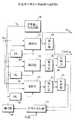
図1は本発明の第1の実施例の説明図であり、1〜3は第1〜第3の識別器、4は基準電圧発生回路、5〜7は積分器、8,9は比較器、10,11は電圧加算器である。基準電圧発生回路4から基準電圧V1を出力し、第1の識別器1にはその基準電圧V1を識別レベルとして加え、第2の識別器2には、電圧加算器10によりΔVを加算してV1+ΔVを識別レベルとして加え、第3の識別器3には、電圧加算器11によりΔVを減算してV1−ΔVを識別レベルとして加える。この場合、基準電圧発生回路4からV1,V1+ΔV,V1−ΔVの電圧を出力する構成とし、且つV1を可変とする構成とすることができる。又積分器5〜7と比較器8,9とを含む構成が制御回路となる。
【0040】
又図示を省略した前段の等化増幅器からの入力データDin(受信信号)が第1〜第3の識別器1〜3に、又図示を省略したタイミング再生部からのクロック信号CLKが第1〜第3の識別器1〜3に加えられ、このクロック信号CLKは後段の回路へのクロック信号CLKoutとして出力される。又クロック信号CLKによる識別位相に於いて、第1の識別器1は、基準電圧V1を第1の識別レベルとして入力データDinを比較して出力データDoutとし、且つ積分器5により積分する。又第2の識別器2は、V1+ΔVを第2の識別レベルとして入力データDinを比較し、積分器6により積分する。又第3の識別器3は、V1−ΔVを第3の識別レベルとして入力データDinを比較し、積分器7により積分する。積分器5〜7の積分時定数は、入力データDin(受信信号)の周期に比較して充分に長い値に設定する。
【0041】
積分器5〜7の出力は、識別出力の平均値を示すことになり、従って、積分器5〜7はローパスフィルタにより構成することも可能であり、又一定時間内の識別出力をカウントするカウンタにより構成することも可能である。比較器8は、第1と第2との識別器1,2の識別出力の平均値を比較し、比較器9は、第1と第3との識別器1,3の識別出力の平均値を比較する。比較器8,9に於ける平均値の比較結果が総て同一であると、識別レベルは最適化されている判定され、基準電圧発生回路4は、基準電圧V1の値を前のまま維持する。
【0042】
図2は本発明の第1の実施例の識別器の動作説明図であり、(A)はアイパターンに於ける識別レベルを示し、基準電圧V1を第1の識別レベル、V1+ΔVを第2の識別レベル、V1−ΔVを第3の識別レベルとした場合であり、LMは識別レベルマージンを示す。
【0043】
基準電圧V1がアイパターンの中心位置を示す場合は、V1+ΔVの第2の識別レベルと、V1−ΔVの第3の識別レベルとによる受信信号の識別出力は総て同一となり、従って、平均値も等しくなる。しかし、アイパターンの中心位置に対して基準電圧V1が相対的に上昇した場合、第2の識別レベルによる受信信号の識別出力は、第1,第3の識別レベルによる受信信号の識別出力と異なる場合が生じ易くなる。反対に、アイパターンの中心位置に対して基準電圧V1が相対的に低下した場合、第3の識別レベルによる受信信号の識別出力は、第1,第2の識別レベルによる受信信号の識別出力と異なる場合が生じ易くなる。
【0044】
例えば、最適な識別レベルによる受信信号の識別出力が、(B)に示す場合、その平均値はVAVR1となる。識別レベルが最適値より上昇すると、同一レベルの受信信号でも“0”と判定する確率が高くなり、例えば、(C)に示す識別出力となる。この場合の平均値はVAVR2となり、VAVR2<VAVR1の関係となり、比較器8,9によって検出することができる。
【0045】
このような関係から、第1の識別器1の識別出力の平均値と第2の識別器2の識別出力の平均値とが等しく、第1の識別器1の識別出力の平均値と第3の識別器3の識別出力の平均値とが異なる場合は、アイパターンの中心位置に対して基準電圧V1が相対的に低下した場合に相当し、基準電圧発生回路4は、比較器9からの平均値の比較相違を示す出力信号によって基準電圧V1を上昇させる。反対に、第1の識別器1の識別出力の平均値と第2の識別器2の識別出力の平均値とが異なる場合は、アイパターンの中心位置に対して基準電圧V1が相対的に上昇した場合に相当し、基準電圧発生回路4は、比較器8からの平均値の比較相違を示す出力信号によって基準電圧V1を低下させる。従って、自動的に識別レベルを最適化することができる。
【0046】
図3は本発明の第2の実施例の説明図であり、11〜13は第1〜第3の識別器、14は基準電圧発生回路、15,16は積分器、17,18は排他的論理和回路、20,21は電圧加算器、22,23は比較器、24は差動増幅器、25,26は基準電圧電源である。積分器15,16と排他的論理和回路17,18と比較器22,23と差動増幅器24とを含めて制御回路が構成されている。
【0047】
第1〜第3の識別器11〜13と、基準電圧V1を出力する基準電圧発生回路14と、基準電圧V1にΔVを加算及び減算する電圧加算器20,21とは、前述の第1の実施例に於ける第1〜第3の識別器1〜3と基準電圧発生回路4と電圧加算器10,11と同様な構成及び作用を行うものであり、重複した説明を省略する。
【0048】
排他的論理和回路17は、第1の識別器11と第2の識別器12との識別出力を比較し、相違する場合の誤りパルスを検出して積分器15に加えて積分する。又排他的論理和回路18は、第1の識別器11と第3の識別器13との識別出力を比較し、相違する場合の誤りパルスを検出して積分器16に加えて積分する。積分器15,16の出力と基準電圧電源25,26の電圧と比較器22,23により比較し、その基準電圧を超えていると、差動増幅器24を介して基準電圧発生回路14に制御信号として加える。
【0049】
図4は本発明の第2の実施例の誤りパルス検出説明図であり、(a)を第1の識別器11の識別出力とし、(b)を第2又は第3の識別器12,13の識別出力とすると、排他的論理和回路17,18の出力は(c)に示すものとなる。この(c)に示す誤りパルスを積分器15,16により積分し、排他的論理和出力の平均値を求める。
【0050】
例えば、基準電圧V1がアイパターンの中心位置に対して相対的に上昇した場合、第1の識別器11の識別出力に対して、第2の識別器12の識別出力が相違する確率が高くなるが、第3の識別器13の識別出力が相違する確率は零に近いものとなる。従って、積分器15の出力が高くなり、基準電圧電源25の電圧を超えると、比較器22の出力が差動増幅器24の−端子に入力され、基準電圧発生回路14に差動増幅器24の負極性の出力信号が入力され、基準電圧発生回路14からの基準電圧V1は低下される。
【0051】
前述の場合と反対に、基準電圧V1がアイパターンの中心位置に対して相対的に低下した場合、第1の識別器11の識別出力に対して、第2の識別器12の識別出力が相違する確率は零に近いが、第3の識別器13の識別出力が相違する確率が高くなり、従って、積分器16の出力が高くなって、基準電圧電源26の電圧を超えると、比較器23の出力が差動増幅器24の+端子に入力され、基準電圧発生回路14に差動増幅器24の正極性の出力信号が入力され、基準電圧発生回路14からの基準電圧V1は上昇される。従って、識別レベルは自動的に最適化される。
【0052】
図5は本発明の第3の実施例の説明図であり、31〜33は基準位相,進み位相,遅れ位相の識別器、34は基準電圧発生回路、35〜37は積分器、38,39は比較器、40〜42は遅延回路(DL)、43は位相可変回路、44は増幅器である。積分器35〜37と比較器38,39とにより位相可変回路43を制御する制御回路を構成している。又図示を省略した前段の等化増幅器からの入力データDin(受信信号)が基準位相,進み位相,遅れ位相の識別器31〜33に加えられ、又図示を省略したタイミング再生部からのクロック信号CLKが、位相可変回路43と増幅器44と遅延回路40〜42とを介してそれぞれ基準位相,進み位相,遅れ位相の識別器31〜33に加えられ、基準位相の識別器31に加えられるクロック信号CLKが、後段の回路へのクロック信号CLKoutとして出力される。又基準位相の識別器31による識別出力が出力データDoutとなる。
【0053】
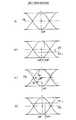
遅延回路40〜42は、基準位相の識別器31に於いて基準位相Φ1を識別位相とし、進み位相の識別器32に於いてΦ1+ΔΦを識別位相とし、遅れ位相の識別器33に於いてΦ1−ΔΦの識別位相とするように、それぞれの遅延時間が設定されている。この場合の位相ΔΦは、アイパターンの位相マージンに対応して選定することができる。又基準電圧発生回路34からの基準電圧V1が、基準位相,進み位相,遅れ位相の識別器31〜33の識別レベルとなる。
【0054】
図6は本発明の第3の実施例の識別位相の説明図であり、(a)はアイパターン、(b)は基準位相の識別器31に加えられるクロック信号、(c)は進み位相の識別器32に加えられるクロック信号、(d)は遅れ位相の識別器33に加えられるクロック信号を示し、基準位相の識別器31は、基準電圧V1を識別レベルとし、基準位相Φ1を識別位相として受信信号を識別する。又進み位相の識別器32は、基準電圧V1を識別レベルとし、Φ1+ΔΦを識別位相として受信信号を識別する。又遅れ位相の識別器33は、基準電圧V1を識別レベルとし、Φ1−ΔΦを識別位相として受信信号を識別する。従って、識別ポイントはP1〜P3となる。又PMは識別位相マージンを示す。この場合、識別位相マージンPM内に入るように、Φ1±ΔΦが選定されている。
【0055】
基準位相Φ1が例えばタイミング再生部の温度変動等によって進み位相となると、Φ1+ΔΦの識別位相による進み位相の識別器32に於ける受信信号の識別に於いて誤り率が増加する。これに対してΦ1−ΔΦの識別位相による遅れ位相の識別器33に於ける受信信号の識別に於いては、基準位相Φ1を識別位相とする基準位相の識別器31に於ける受信信号の識別の誤り率とほぼ同一となる。従って、積分器35,37の積分出力はほぼ同一となるが、積分器35,36の積分出力は異なるものなり、比較器38の出力信号が位相可変回路43に加えられて、基準位相Φ1がアイパターンの中心位置に戻るように遅れ位相制御が行われる。
【0056】
反対に、基準位相Φ1がアイパターンの中心位置から遅れ位相となると、Φ1−ΔΦの識別位相による遅れ位相の識別器33に於ける受信信号の識別に於いて誤り率が増加し、積分器35,36の積分出力はほぼ同一となるが、積分器35,37の積分出力は相違することになり、比較器39の出力信号が位相可変回路43に加えられて、基準位相Φ1がアイパターンの中心位置に戻るように進み位相制御が行われる。従って、識別位相を自動的に最適化することができる。
【0057】
図7は本発明の第4の実施例の説明図であり、51〜53は基準位相,進み位相,遅れ位相の識別器、54は基準電圧発生回路、55,56は積分器、57,58は排他的論理和回路、60〜62は遅延回路(DL)、63は位相可変回路、64は増幅器、66,67は比較器、68は差動増幅器であり、積分器55,56と排他的論理和回路57,58と比較器66,67と差動増幅器68とにより、位相可変回路63を制御する制御回路を構成している。又図示を省略した前段の等化増幅器からの入力データDin(受信信号)が、基準位相,進み位相,遅れ位相の識別器51〜53に加えられ、又図示を省略したタイミング再生部からのクロック信号CLKが、基準位相,進み位相,遅れ位相の識別器51〜53に加えられ、このクロック信号CLKは後段の回路へのクロック信号CLKoutとして出力される。又基準位相の識別器51による識別出力が出力データDoutとなる。
【0058】
基準位相Φ1がアイパターンの中心位置から例えば進み位相となると、前述の場合と同様に、基準位相の識別器51の識別出力と遅れ位相の識別器53の識別出力とはほぼ同一となるから、排他的論理和回路58の出力信号は殆ど“0”の連続となるが、基準位相の識別器51の識別出力と進み位相の識別器52の識別出力とは相違する確率が大きくなり、それに対応して排他的論理和回路57の出力信号が“1”となる。従って、積分器55の積分出力が大きくなり、比較器66の基準電圧を超えると、差動増幅器68の−端子に比較器66の出力信号が加えられて、負極性の信号が位相可変回路63に加えられ、基準位相Φ1がアイパターンの中心位置に戻るように遅れ位相制御が行われる。
【0059】
反対に、基準位相Φ1がアイパターンの中心位置から遅れ位相となると、基準位相及び進み位相の識別器51,52の識別出力はほぼ同一となるが、基準位相及び遅れ位相の識別器51,53の識別出力が相違する確率が大きくなり、それによって、積分器56の積分出力が大きくなり、比較器67の基準電圧を超えると、差動増幅器68の+端子に比較器67の出力信号が加えられて、正極性の信号が位相可変回路63に加えられ、基準位相Φ1がアイパターンの中心位置に戻るように進み位相制御が行われる。従って、識別位相を自動的に最適化することができる。
【0060】
図8は本発明の第5の実施例の説明図であり、71,72は第1,第2の識別器、73は比較器、74は基準電圧発生回路、75は電圧変調回路、76,77は積分器であり、積分器76,77と比較器73とにより基準電圧発生回路74を制御する制御回路を構成している。又図示を省略した前段の等化増幅器からの入力データDin(受信信号)が第1,第2の識別器71,72に入力され、又図示を省略したタイミング再生部からのクロック信号CLKが第1,第2の識別器71,72に加えられる。
【0061】
又基準電圧発生回路74からの基準電圧V1が第1の識別器71の識別レベルとして加えられる。又電圧変調回路75に於いて基準電圧V1を入力データDinの速度に比較して充分に遅い速度で周波数変調した電圧V1±ΔVが第2の識別器72に識別レベルとして加えられる。又第1の識別器71の識別出力が出力データDoutとなる。
【0062】
図9は本発明の第5の実施例の識別レベルの説明図であり、(a)は、第1の識別器71に於ける基準電圧V1による識別レベルにより、受信信号を識別する場合を示し、(b)は、第2の識別器72に於けるV1±ΔVの周波数変調識別レベルにより、受信信号を識別する場合を示す。このV1±ΔVのレベルが識別レベルマージンLMの範囲内であれば、第1,第2の識別器71,72の識別出力はほぼ等しいものとなり、従って、積分器76,77の積分出力を比較器73により比較すると、ほぼ等しいものとなるから、基準電圧発生回路74からの基準電圧V1はそのままの状態を維持させる。
【0063】
例えば、基準電圧V1が上昇して、V1+ΔVが識別レベルマージンLMの範囲を超えると、第1の識別器71に比較して第2の識別器72が“1”と識別する確率が低くなる。従って、積分器76の積分出力が積分器77の積分出力より大きくなり、比較器73はその積分出力の差に対応して基準電圧発生回路74を制御し、基準電圧V1を低下させる。
【0064】
反対に、基準電圧V1が低下し、V1−ΔVが識別レベルマージンLMの範囲を超えると、第1の識別器71に比較して第2の識別器72が“0”と識別する確率が低くなる。従って、積分器76の積分出力が積分器77の積分出力より小さくなり、比較器73はその積分出力の差に対応して基準電圧発生回路74を制御し、基準電圧V1を上昇させる。従って、基準電圧V1を自動的に最適化することができる。
【0065】
図10は本発明の第6の実施例の説明図であり、81,82は第1,第2の識別器、83は排他的論理和回路、84は基準電圧発生回路、85は電圧変調回路、86,87はゲート回路、88,89は積分器、90はゲート制御回路、91,92は比較器、93は差動増幅器であり、排他的論理和回路83とゲート回路86,87と積分器88,89と比較器91,92と差動増幅器93とゲート制御回路90とにより、基準電圧発生回路84を制御する制御回路を構成している。
【0066】
図示を省略した前段の等化増幅器からの入力データDin(受信信号)が第1,第2の識別器81,82に入力され、又図示を省略したタイミング再生部からのクロック信号CLKが第1,第2の識別器81,82に加えられる。又基準電圧発生回路84からの基準電圧V1が第1の識別器81の識別レベルとして加えられる。又電圧変調回路85に於いて基準電圧V1を入力データ速度に比較して充分に遅い速度で周波数変調した電圧V1±ΔVが第2の識別器82に識別レベルとして加えられる。
【0067】
前述の実施例と同様に、第1の識別器81は、基準電圧V1を識別レベルとし、クロック信号CLKの位相を識別位相として入力データDinを識別し、第2の識別器82は、V1±ΔVを識別レベルとし、クロック信号CLKの位相を識別位相として入力データDinを識別するもので、基準電圧V1がアイパターンの中心位置近傍であれば、第1,第2の識別器81,82の識別出力は同一となる。従って、排他的論理和回路83の出力は“0”となる。
【0068】
又ゲート制御回路90は相補出力の比較器により構成した場合を示し、基準電圧V1とそれを周波数変調した電圧VM=V1±ΔVとを比較し、例えば、V1>VMの期間はゲート回路86を開き、V1<VMの期間はゲート回路87を開くゲート制御信号を出力し、排他的論理和回路83の出力を積分器88,89に分配する。このゲート制御回路90は、電圧変調回路85に於ける周波数変調信号を用いてゲート制御信号を形成する構成とすることも可能である。
【0069】
図11は本発明の第6の実施例のゲート制御の説明図であり、(a)は基準電圧V1を識別レベルとする第1の識別器81の識別出力の一例を示し、(b)は電圧変調回路85に於ける変調信号の一例を示す。又(c)は、基準電圧V1と周波数変調した電圧VMとを比較して非反転端子からの出力するゲート制御信号を示す。即ち、変調信号が正極性の時に“1”、負極性の時に“0”のゲート制御信号となる。又(d)は周波数変調した電圧VMを識別レベルとする第2の識別器82の識別出力の一例を示す。
【0070】
従って、排他的論理和回路83からの(a)と(d)との識別出力の排他的論理和出力は、(c)に示すゲート制御信号が“1”(V1+ΔV)の期間に於いて(e)に示すように積分器88に加えられ、“0”(V1−ΔV)の期間に於いて(f)に示すように積分器89に加えられる。積分器88,89の積分出力はそれぞれ比較器91,92により基準電圧と比較され、基準電圧を超えると差動増幅器93の正極性又は負極性の出力が基準電圧発生回路84に加えられて、基準電圧V1をアイパターンの中心位置方向に補正するような制御が行われる。即ち、基準電圧V1の最適化が行われる。
【0071】
図12は本発明の第7の実施例の説明図であり、101,102は基準位相及び変調位相の識別器、103は位相可変回路、104は基準電圧発生回路、105,106は識別器、107は積分比較器、108は増幅器、109は位相変調増幅器である。入力データDinを、基準電圧発生回路104からの基準電圧V1を識別レベルとし、位相可変回路103と増幅器108とを介したクロック信号CLKの位相を識別位相として識別器101で識別し、又基準電圧V1を識別レベルとし、位相可変回路103と位相変調増幅器109とを介したクロック信号CLKの位相を識別位相として識別器102で識別する。
【0072】
位相変調増幅器109は、位相可変回路103により位相が制御されたクロック信号の位相を、入力データDinの速度に比較して遅い速度で周波数変調する。従って、変調位相の識別器102は、基準位相をΦ1とすると、Φ1±ΔΦの位相変調された識別位相で識別することになる。又識別器105,106は、基準電圧V1を識別レベルとし、基準位相Φ1を識別位相として、それぞれ基準位相及び変調位相の識別器101,102の識別出力を識別するもので、例えばフリップフロップにより構成することができる。それによって、基準位相及び変調位相の識別器101,102の識別出力の位相を一致させることができる。そして、識別器105の識別出力を出力データDoutとし、基準位相Φ1のクロック信号CLKoutを後段の回路へ出力する。
【0073】
積分比較器107は、識別器105,106の出力をそれぞれ積分して比較する構成を有し、基準位相Φ1がアイパターンの中心位置近傍の場合は、第1,第2の識別器101,102の識別出力は等しくなり、基準位相Φ1が進み位相又は遅れ位相となって、Φ1+ΔΦ又はΦ1−ΔΦが識別位相マージンを超えると識別出力が相違することになり、積分比較器107により位相可変回路103を制御して、基準位相Φ1をアイパターンの中心位置方向にシフトさせる。
【0074】
図13は本発明の第7の実施例の位相変調の説明図であり、(a)は、クロック信号CLKと変調信号Fとを比較する比較器COMPにより、位相変調増幅器109を構成した場合を示す。又(b)はクロック信号CLK、(c)は変調信号Fのそれぞれ一例を示し、(d)は比較器COMPの出力信号を示す。即ち、立上り位相が周波数変調されたものとなり、この立上り位相を識別位相として、第2の識別器102に於いて入力データDinの識別を行うことになる。
【0075】
図14は本発明の第7の実施例の識別位相の説明図であり、(a)はアイパターンに於ける識別ポイントP1,P2,P3を示し、(b)は基準位相Φ1のクロック信号、(c)は周波数変調されたクロック信号を示す。又位相の変調範囲は、識別位相マージンPMの範囲内に設定した場合を示す。(a)のアイパターンに於いて、(b)に示すクロック信号による識別ポイントはP1となる。しかし、(c)に示すクロック信号による識別ポイントは、P2からP3に向かって、又P3からP2に向かって矢印のように変化する。
【0076】
従って、基準位相Φ1がアイパターンの中心位置近傍であると、基準位相及び変調位相の識別器101,102の識別出力は等しくなり、基準位相Φ1がアイパターンの中心位置近傍から進み位相又は遅れ位相となると、変調位相の識別器102の識別誤りが増加するから、積分比較器107に於ける基準位相及び変調位相の識別器101,102の識別出力を積分した値が異なるものとなり、位相可変回路103を制御して基準位相Φ1をアイパターンの中心位置方向にシフトするように制御する。従って、基準位相Φ1を自動的に最適化することができる。
【0077】
図15は本発明の第7の実施例の識別出力の同期説明図であり、(a)は基準位相Φ1のクロック信号、(b)は基準位相の識別器101の識別出力、(c)は変調位相の識別器102の識別出力、(d),(e)は識別器105,106の出力を示す。即ち、基準位相の識別器101の識別出力は、基準位相Φ1を識別位相として(b)に示すものとなるが、変調位相の識別器102の識別出力は、Φ1±ΔΦを識別位相として(c)に示すように±ΔΦの位相変動が生じているものとなる。
【0078】
そこで、同一のクロック信号を加えるフリップフロップ等による識別器105,106を設けることにより、基準位相の識別器101の識別出力は(d)に、又変調位相の識別器102の識別出力は(e)にそれぞれ示すように、同一の位相として出力することができる。従って、基準位相の識別器101と変調位相の識別器102との識別出力の積分処理や比較処理の精度を向上することができる。
【0079】
図16は本発明の第8の実施例の説明図であり、111,112は基準位相及び変調位相の識別器、113は位相可変回路、114は基準電圧発生回路、115,116は識別器、117は排他的論理和回路、118は増幅器、119は位相変調増幅器、120はゲート制御回路、121,122は比較器、123は差動増幅器、126,127はゲート回路、128,129は積分器である。
【0080】
この実施例に於いては、図12に示す実施例の制御回路に、図10に示す制御回路を適用した場合に相当し、識別出力の位相を識別器115,116によって一致させて、排他的論理和回路117により識別出力を比較し、不一致の場合の出力信号を、ゲート制御回路120からのゲート制御信号によって積分器128,129に分配する。
【0081】
従って基準位相Φ1がアイパターンの中心位置近傍からずれると、基準位相及び変調位相の識別器111,112の識別出力が相違し、それによって、位相がシフトした側の積分器128,129の積分出力が大きくなり、比較器121,122と差動増幅器123とにより位相を元の方向に戻すように、位相可変回路113を制御することになる。従って、基準位相Φ1を自動的に最適位相に制御することができる。
【0082】
図17は本発明の第9の実施例の説明図であり、131〜133は第1〜第3の識別器、134は基準電圧発生回路、135,136は識別器、137は排他的論理和回路、138は増幅器、139は位相変調増幅器、140はゲート制御回路、141は電圧変調回路、142は比較器、143,144は積分器、145は比較器、146,147はゲート回路、148,149は積分器、150は位相可変回路である。
【0083】
この実施例は、図8に示す実施例と、図16に示す実施例とを組合せた場合に相当し、各実施例と重複する説明は省略する。この実施例に於いては、第1の識別器131は、基準電圧V1及び基準位相Φ1を識別レベル及び識別位相として入力データDinを識別し、第2の識別器132は、電圧変調回路141によるV1±ΔVを識別レベル、基準位相Φ1を識別位相として識別し、第3の識別器133は、基準電圧V1を識別レベル、位相変調増幅器139からのΦ1±ΔΦを識別位相として識別し、識別器135,136は識別出力の位相を一致させて排他的論理和回路137に加えるものである。
【0084】
即ち、第1,第2の識別器131,132により基準電圧V1がアイパターンの中心位置近傍であるか否かを識別する為に用いられ、第1,第3の識別器131,133により基準位相Φ1がアイパターンの中心位置近傍であるか否かを識別する為に用いられ、第1の識別器131を両者に共用している。
【0085】
又積分器143,144と比較器142とにより電圧制御回路を構成して、基準電圧発生回路134を制御し、自動的に基準電圧V1の最適化を図り、又排他的論理和回路137とゲート回路146,147と積分器148,149とゲート制御回路140と比較器145とにより位相制御回路を構成して、位相可変回路150を制御して、自動的に基準位相Φ1の最適化を図ることができる。
【0086】
図18は本発明の第9の実施例の変調制御の説明図であり、(A),(B)はアイパターンに対する変調電圧と変調位相とによる識別範囲を示す。(A)に於いて、識別マージンをMaで示すと、その識別マージンMaの範囲内となるように、基準電圧V1を2ΔVaの範囲に変調し、基準位相Φ1を2ΔΦaの範囲に変調する。即ち、V1±ΔVaの変調電圧を第2の識別器132の識別レベルとして加える。又Φ1±ΔΦaの変調位相を第3の識別器133の識別位相として加える。
【0087】
従って、基準電圧V1の変調範囲と基準位相Φ1の変調範囲とが識別マージンMaの範囲内となるように、前述の各実施例と同様に、基準電圧V1及び基準位相Φ1を自動的に最適化できることになる。
【0088】
又アイパターンは、受信信号パワーが大きい時は大きく開くものであり、反対に受信信号パワーが小さい時は開きが小さくなる。そこで、光通信システムに於いては、受信光パワーを検出し、又光通信システムを含む一般的な通信システムに於いて、AGC増幅器に於けるAGC電圧等を検出し、基準電圧V1及び基準位相Φ1の変調度を制御することができる。
【0089】
即ち、図18の(A)を受信信号パワーがPW1の時のアイパターンとすると、前述のように、基準電圧V1を2ΔVaの範囲且つ基準位相Φ1を2ΔΦaの範囲となるように変調度を制御する。又受信信号パワーが小さくなってPW2となると、(B)に示すように、アイパターンの開きが小さくなる。その場合は、基準電圧V1を2ΔVbの範囲で且つ基準位相Φ1を2ΔΦbの範囲となるように変調度を制御し、識別マージンMbの範囲となるように、基準電圧V1及び基準位相Φ1を制御する。その場合の変調度は、電圧変調回路141及び位相変調増幅器139に、前述の受信信号パワーの検出信号を加えることにより制御することができる。
【0090】
図19は本発明の第10の実施例の説明図であり、151〜153は第1〜第3の識別器、154は基準電圧発生回路、155,156は識別器、157は排他的論理和回路、158は増幅器、159は位相変調増幅器、160はゲート制御回路、161は電圧変調回路、162は比較器、163は排他的論理和回路、164はゲート制御回路、165は比較器、166,167,171,172はゲート回路、168,169,173,174は積分器、170は位相可変回路である。
【0091】
この実施例は、図10に示す実施例と図16に示す実施例とを組合せた構成に相当し、第1〜第3の識別器152〜153は図17に示す実施例に於ける第1〜第3の識別器131〜133と同一の構成及び作用を行うものであり、重複した説明を省略する。この実施例に於いて、排他的論理和回路157とゲート回路166,167とゲート制御回路160と積分器168,169と比較器165とからなる位相制御回路によって位相可変回路170を制御して基準位相Φ1を最適化し、又排他的論理和回路163とゲート回路171,172とゲート制御回路164と積分器173,174と比較器162とからなる電圧制御回路によって基準電圧発生回路154を制御して基準電圧V1を最適化することができる。従って、無調整で識別ポイントを最適な位置に設定することが可能となる。
【0092】
図20は本発明の第11の実施例の説明図であり、181,182は第1,第2の識別器、183は発振器、184は基準電圧発生回路、185,186は第4,第5の識別器、187は排他的論理和回路、188は増幅器、189は位相変調増幅器、190,194はゲート制御回路、191は電圧変調回路、192,195は比較器、193は90度移相器、196,197,201,202はゲート回路、198,199,203,204は積分器、200は位相可変回路である。
【0093】
この実施例は、発振器183の出力信号を、位相変調増幅器189に変調信号として加えると共に、90度移相器193を介して電圧変調回路191に変調信号として加えるもので、位相変調増幅器189と電圧変調回路191とは、90度の位相差の同一周波数の変調信号によって基準位相Φ1及び基準電圧V1の変調を行うものである。この変調電圧を識別レベルとし、且つ変調位相を識別位相として入力データDinを識別する第2の識別器182に於ける識別ポイントは、アイパターンに対して円或いは楕円を描くように変化する。
【0094】
又第1の識別器181は、基準電圧V1を識別レベルとし、且つ基準位相Φ1を識別位相として入力データDinを識別し、出力データDoutとすると共に、基準位相Φ1のクロック信号CLKoutを後段の回路へ送出する。第4,第5の識別器185,186はフリップフロップによって構成し、異なる位相の第1,第2の識別器181,182の識別出力を同一位相とするものである。そして、排他的論理和回路187によって識別出力を比較し、この比較出力を変調周波数の周期に対応したゲート制御回路194,190からのゲート制御信号によって分配する。
【0095】
即ち、V1+ΔVの期間の比較出力を積分器203に、V1−ΔVの期間の比較出力を積分器204に分配し、Φ1+ΔΦの期間の比較出力を積分器198に、Φ1−ΔΦの期間の比較出力を積分器199に分配する。そして、比較器192により積分器203,204の積分出力を比較して基準電圧発生回路184を制御し、基準電圧V1をアイパターンの中心位置近傍となるように制御し、比較器195により積分器198,199の積分出力を比較して位相可変回路200を制御し、基準位相Φ1をアイパターンの中心位置近傍となるように制御する。
【0096】
図21は本発明の第11の実施例の識別動作説明図であり、(a)はアイパターンに於ける識別ポイントを示し、(b)は発振器183から位相変調増幅器189に加えられる変調信号F1と90度移相器193を介して電圧変調回路191に加えられる変調信号F2とを示す。90度位相差の変調信号に従ってアイパターンに於ける識別ポイントが例えば矢印方向に回転する。その場合の変調度を点線で示す識別マージンの範囲内となるように選定する。
【0097】
又(c)〜(f)はゲート制御信号の一例を示し、(c)は基準電圧V1に対して+領域の変調電圧の時にゲート回路201を開くゲート制御信号、(e)は−領域の変調電圧の時にゲート回路202を開くゲート制御信号、(d)は基準位相Φ1に対して進み位相領域の時にゲート回路196を開くゲート制御信号、(f)は遅れ位相領域の時にゲート回路197を開くゲート制御信号である。このようなゲート制御信号は、(b)に示す変調信号F1,F2のレベル比較によって容易に形成することができる。
【0098】
(c)〜(f)に示すゲート制御信号の場合は、排他的論理和回路187の出力信号をそれぞれ積分器に分配することになるが、前述のように、V1+ΔVの期間とV1−ΔVの期間とに対応してゲート回路201,202を制御し、Φ1+ΔΦの期間とΦ1−ΔΦの期間とに対応してゲート回路196,197を制御し、例えば、V1+ΔVで且つΦ1+ΔΦの期間の排他的論理和回路187の出力信号を電圧制御回路側と位相制御回路側との積分器に分配するように構成することも可能である。
【0099】
前述の各実施例に於いて、受信信号パワーを検出し、基準電圧V1の変調度と基準位相Φ1の変調度との何れか一方又は両方を制御することができる。この場合の受信信号パワーの検出手段は、光通信システムに於いては受信光パワーを検出する構成又はAGC増幅器のAGC電圧を検出する構成等を適用できる。又受信信号断検出を行った時に、基準電圧V1及び基準位相Φ1の制御を停止させる構成を設けることもできる。このような構成は、公知の受信信号断検出回路の検出信号を基準電圧発生回路又は位相可変回路に加えることにより実現することができる。又基準電圧V1又は基準位相Φ1の変調度を識別マージンを超える程度に設定し、誤り率曲線を基に基準電圧V1又は基準位相Φ1を制御する構成とすることも可能である。
【0100】
【発明の効果】
以上説明したように、本発明は、基準電圧V1と基準位相Φ1との何れか一方又は両方について、基準電圧V1を識別レベルとし、又基準位相Φ1を識別位相とした識別出力に対して、基準電圧V1を+ΔVと−ΔVとにシフトした電圧を識別レベルとした時の識別出力、又は基準位相Φ1を+ΔΦと−ΔΦとにシフトした位相を識別位相とした時の識別出力との差分を基に、基準電圧V1又は基準位相Φ1を制御するもので、無調整で基準電圧V1又は基準位相Φ1を最適化することができる利点がある。又経年変化,温度変化,電源電圧変化等による基準電圧V1の変化や基準位相Φ1の変化が発生した場合も、自動的に補正するように制御することになり、従って、常に最適な基準電圧V1と基準位相Φ1を得ることができる利点がある。
【0101】
又基準電圧V1又は基準位相Φ1を周波数変調することにより、識別器の個数を削減することが可能となる。又基準電圧V1と基準位相Φ1との変調周波数を同一とし且つ90度の位相差を与えることにより、アイパターンに対して円又は楕円の軌跡の識別ポイントが得られるから、アイパターンの歪みが大きい場合に於いても、最適な基準電圧V1と基準位相Φ1とに制御することができる利点がある。
【0102】
入力信号パワー等の各種の条件を基に、基準電圧V1に対するΔVの大きさ及び基準位相Φ1に対するΔΦの大きさ、或いは周波数変調を行う場合の変調度を制御することにより、アイパターンの開きの大小に対応した識別マージンの範囲に従って、最適識別レベルの制御及び最適識別位相の制御が可能となる利点がある。
【図面の簡単な説明】
【図1】本発明の第1の実施例の説明図である。
【図2】本発明の第1の実施例の識別器の動作説明図である。
【図3】本発明の第2の実施例の説明図である。
【図4】本発明の第2の実施例の誤りパルス検出説明図である。
【図5】本発明の第3の実施例の説明図である。
【図6】本発明の第3の実施例の識別位相の説明図である。
【図7】本発明の第4の実施例の説明図である。
【図8】本発明の第5の実施例の説明図である。
【図9】本発明の第5の実施例の識別レベルの説明図である。
【図10】本発明の第6の実施例の説明図である。
【図11】本発明の第6の実施例のゲート制御の説明図である。
【図12】本発明の第7の実施例の説明図である。
【図13】本発明の第7の実施例の位相変調の説明図である。
【図14】本発明の第7の実施例の識別位相の説明図である。
【図15】本発明の第7の実施例の識別出力の同期説明図である。
【図16】本発明の第8の実施例の説明図である。
【図17】本発明の第9の実施例の説明図である。
【図18】本発明の第9の実施例の変調制御の説明図である。
【図19】本発明の第10の実施例の説明図である。
【図20】本発明の第11の実施例の説明図である。
【図21】本発明の第11の実施例の識別動作説明図である。
【図22】光受信器の概要説明図である。
【図23】識別動作説明図である。
【符号の説明】
1 第1の識別器
2 第2の識別器
3 第3の識別器
4 基準電圧発生回路
5〜7 積分器
8,9 比較器
10,11 電圧加算器[0001]
[Industrial applications]
The present invention relates to an identification circuit for reproducing data by level identification.
Since the waveform of the received signal has undergone transmission distortion, the data is reproduced by comparing it with a predetermined level in the identification circuit. It is necessary to optimize the identification level and the identification phase in that case.
[0002]
[Prior art]
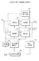
FIG. 22 is a schematic explanatory view of an optical receiver, wherein 301 is a light receiving element such as a pin diode, 302 is an output resistor, 303 is a preamplifier, 304 is a resistor, 305 is an equalizing amplifier, 306 is an identification circuit, 307 Denotes a timing reproducing unit, 308 denotes a differential extractor, 309 denotes a filter such as a surface acoustic wave filter, and 310 denotes an amplifier.
[0003]
An optical signal intensity-modulated by the transmission data is transmitted through an optical fiber transmission line, the optical signal is incident on a
[0004]
The
[0005]
[Problems to be solved by the invention]
As described above, in the
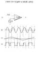
[0006]
FIG. 23 is an explanatory diagram of the discriminating operation. FIG. 23A shows the case of the ideal state, in which the discrimination level DL and the discrimination phase DP are set such that the center position of the eye pattern indicated by the black circle is the discrimination point. Show the case. (B) shows that even if the
[0007]
(C) shows the case where the discrimination level DL and the discrimination phase DP are the same as in (A), but the waveform distortion is large and the solid line eye pattern changes as shown by the dashed line. Assuming that the margin in the case of the eye pattern is M, the margin in the case of the one-dot chain line eye pattern is M1 And the error rate is degraded. (D) shows that the discrimination level DL is changed according to temperature change, aging change, power supply voltage change and the like.2 And the discrimination phase DP is DP2 Shows the case where it has changed. Also in this case, the identification level DL2 And identification phase DP2 If the error rate is not corrected, the error rate deteriorates. Error rate degradation also occurs for various noises (noise due to spontaneous emission light, stimulated Brillouin scattering, self-phase modulation, etc.) generated when the optical amplifier is applied.
[0008]
However, in the conventional
An object of the present invention is to automatically optimize a discrimination level and a discrimination phase without adjustment.
[0009]
[Means for Solving the Problems]
The identification circuit of the present invention will be described with reference to FIG. 1. (1) In the identification circuit for identifying a received signal using an identification level and in an identification phase, a reference voltage V1 With the received signal Din A
[0010]
(2) Reference voltage V1 With the received signal Din A
[0011]
(3) A reference phase discriminator for identifying a received signal using the reference phase as a first discrimination phase, and an advance phase discriminator for discriminating the reception signal using this reference phase as a predetermined advance phase as a second discrimination phase. A discriminator, a discriminator for a lag phase for discriminating a received signal with a predetermined lag phase as a third discrimination phase with respect to the reference phase, an average value of discrimination outputs of the discriminator for the reference phase, and a leading phase and a lag phase And a control circuit for controlling the reference phase so that the average value of the discrimination output of the discriminator becomes equal.
[0012]
(4) a reference phase discriminator for identifying the received signal using the reference phase as the first discrimination phase, an advanced phase discriminator for identifying the received signal using a predetermined advance phase with respect to the reference phase as the identification phase, A lag phase discriminator for discriminating a received signal as a predetermined lag phase with respect to a reference phase as a discrimination phase, an average value of an exclusive OR of discrimination outputs of a reference phase discriminator and a lead phase discriminator, A control circuit for controlling the reference phase based on an average value of the exclusive OR of the discrimination outputs of the reference phase discriminator and the lag phase discriminator.
[0013]
(5) a first discriminator for discriminating a received signal using the reference voltage as a first discrimination level, and a second discrimination level for a voltage obtained by frequency-modulating the reference voltage at a smaller speed than the transmission speed of the received signal. A second discriminator for discriminating a received signal, a control circuit for controlling a reference voltage such that an average value of the discrimination output of the first discriminator is equal to an average value of the discrimination output of the second discriminator. It has.
[0014]
(6) A first discriminator for discriminating a received signal using a reference voltage as a first discrimination level, and a voltage obtained by frequency-modulating the reference voltage at a speed smaller than the reception transmission speed as a second discrimination level. A second discriminator for discriminating the received signal, and an exclusive OR output of the discrimination output of the first discriminator and the discrimination output of the second discriminator are selected at a period according to the frequency modulation of the reference voltage. And a control circuit for determining an average value and controlling a reference voltage according to the average value.
[0015]
(7) Also, a reference phase discriminator for discriminating a received signal by using the reference phase as a discrimination phase, a modulation phase discriminator for discriminating a received signal by a discrimination phase obtained by modulating the reference phase, and a discrimination output of the reference discriminator. A control circuit for controlling the reference phase so that the average value and the average value of the discrimination output of the discriminator of the modulation phase become equal.
[0016]
(8) A reference phase discriminator for discriminating a received signal using the reference phase as a discrimination phase, a modulation phase discriminator for discriminating a received signal by a discrimination phase obtained by modulating the reference phase, and a discrimination output of the reference discriminator. A control circuit for selecting an exclusive OR output of the discrimination output of the discriminator of the modulation phase and the discrimination output of the discrimination unit according to the modulation cycle of the reference phase to obtain an average value, and controlling the reference phase according to the average value.
[0017]
(9) It is also possible to provide a discriminator operating at the same phase for outputting the discrimination outputs of the reference phase discriminator and the modulation phase discriminator as the same phase.
[0018]
(10) A first discriminator for discriminating a received signal using a reference voltage as a discrimination level and a reference phase as a discrimination phase, a discrimination level using a frequency-modulated reference voltage as a discrimination level, and a discrimination phase for the reference phase. A second discriminator for discriminating the received signal, a third discriminator for discriminating the received signal with the reference voltage as the discrimination level and a phase obtained by frequency-modulating the reference phase as the discrimination phase, and a discrimination output of the first discriminator Voltage control circuit for controlling the reference voltage so that the average value of the first and second discriminators is equal to each other, and exclusive logic of the first and third discriminator discrimination outputs. A phase control circuit for selecting the sum output in accordance with the modulation period of the reference phase, obtaining an average value, and controlling the reference phase in accordance with the average value.
[0019]
(11) Also, a first discriminator for discriminating a received signal using a reference voltage as a discrimination level and a reference phase as a discrimination phase, receiving a voltage obtained by frequency-modulating the reference voltage as a discrimination level, and receiving the reference phase as a discrimination phase. A second discriminator for discriminating a signal, a third discriminator for discriminating a received signal with a reference voltage as a discrimination level, and a phase obtained by frequency-modulating the reference phase as a discrimination phase, and a discrimination output of the first discriminator; A voltage control circuit for selecting an exclusive-OR output with the identification output of the second discriminator in accordance with the modulation period of the reference voltage, obtaining an average value, and controlling the reference voltage in accordance with the average value; A phase control circuit for selecting an exclusive-OR output of the discrimination output of the third discriminator and the discrimination output of the third discriminator according to the modulation period of the reference phase to obtain an average value, and controlling the reference phase according to the average value. ing.
[0020]
(12) It is also possible to provide a discriminator operating in the same phase for obtaining an exclusive OR output by setting the respective discriminant outputs of the first discriminator and the third discriminator in the preceding paragraph to be the same phase. .
[0021]
(13) A first discriminator for discriminating the received signal with the reference voltage as the discrimination level and the reference phase as the discrimination phase, a voltage obtained by frequency-modulating the reference voltage as the discrimination level, and the reference phase as the reference voltage. A second discriminator for discriminating a received signal using a phase modulated at a frequency equal to the modulation frequency and having a phase difference of π / 2 as a discrimination phase, and discriminating outputs of the first discriminator and the second discriminator. Fourth and fifth discriminators each including a flip-flop for obtaining the same phase, an exclusive-OR circuit for obtaining an exclusive OR of the discrimination outputs of the fourth and fifth discriminators, The output of the OR circuit is selected according to the modulation period of the reference voltage to obtain an average value, and the voltage control circuit that controls the reference voltage according to the average value, and the output of the exclusive OR circuit is output according to the modulation period of the reference phase. Select and average Determined, and a phase control circuit for controlling the reference phase according to the average value.
[0022]
(14) Further, the voltage control circuit and the phase control circuit have a configuration for controlling the modulation degree of the reference voltage and the modulation degree of the reference phase in accordance with the detection signal of the power of the received signal by the detection means.
[0023]
[Action]
(1) The
[0024]
The received signal is a case where the mark rate is coded so as to be 、, for example, the reference voltage V1 Is lower than the center position of the eye-pan and no error occurs in the identification output of the
[0025]
(2) The exclusive OR output of the discrimination outputs of the
[0026]
(3) The discrimination levels of the
[0027]
(4) The exclusive OR output of the discrimination output of the reference phase discriminator and the discrimination output of the advance phase discriminator, and the exclusive output of the discrimination output of the reference phase discriminator and the discrimination output of the lag phase discriminator. The OR output indicates whether or not the discrimination outputs of the discriminators are different from each other. Therefore, the average value of the respective exclusive OR outputs is obtained. If each of the outputs is zero or equal, the reference phase is optimal. Otherwise, the reference phase is controlled by the control circuit according to the average value. That is, the identification phase can be automatically optimized.
[0028]
(5) The
[0029]
(6) Also, based on the identification output of the first discriminator, the difference between the discrimination output of the first discriminator and the second discriminator is determined by the exclusive OR with the discrimination output of the second discriminator. And the reference voltage V1 The exclusive OR output is selected in a modulation period obtained by modulating the signal to ± ΔV. That is, V1 + ΔV, the exclusive OR output during the period1 An exclusive logic output during the period of −ΔV is selected and an average value is obtained. Then, the reference voltage V from the reference
[0030]
(7) Reference phase Φ1 Is used as a discrimination phase, the received signal is discriminated by the discriminator of the reference phase, and the reference phase Φ1 The received signal is identified by a modulation phase identifier using a modulation phase obtained by modulating the signal so as to be ± ΔΦ as an identification phase, and an average value of the respective identification outputs is obtained and compared. If the average value is equal, the phase is the optimal phase.If the average value is different, the reference phase Φ1 Is controlled by a control circuit. Thereby, the identification phase can be optimized.
[0031]
(8) Reference phase Φ1 Is used as a discrimination phase, the received signal is discriminated by the discriminator of the reference phase, and the reference phase Φ1 The received signal is identified by a discriminator for the modulated phase, using a modulation phase obtained by modulating the signal so as to be ± ΔΦ as an identification phase, and an exclusive-OR output of each identification output is selected according to a modulation cycle to obtain an average value. That is, Φ1 + ΔΦ during the exclusive OR output and Φ1 An exclusive OR output during a period of −ΔΦ is selected to obtain an average value. When the average value is zero or equal, the phase is the optimum phase. Therefore, when the average value is different, the reference phase Φ corresponds to the difference.1 Is controlled by a control circuit. Thereby, the identification phase can be optimized.
[0032]
(9) Since the discriminator for the reference phase and the discriminator for the modulation phase discriminate the received signal with different phases, the discrimination output has different phases. Therefore, the discrimination outputs having different phases are made to have the same phase by a discriminator such as a flip-flop operated by the same clock signal CLK.
[0033]
(10) The first discriminator uses the reference voltage V1 And the reference phase Φ1 Is used as an identification phase to identify a received signal.1 Is frequency-modulated (V1 ± ΔV) as the discrimination level, and the reference phase Φ1 Is used as an identification phase to identify a received signal.1 And the reference phase Φ1 Is the frequency-modulated phase (Φ1 The received signal is identified using ± ΔΦ) as the identification phase. Then, the reference voltage V is set so that the average values of the discrimination outputs of the first discriminator and the second discriminator become equal.1 Is controlled by a voltage control circuit, and the exclusive OR output of the discrimination outputs of the first discriminator and the third discriminator is changed to a reference phase Φ1 And an average value is determined in accordance with the modulation cycle of That is, Φ1 + ΔΦ period and Φ1 The average value of the exclusive logical outputs during the period of -ΔΦ is obtained. When the respective average values are equal, the phase is the optimum phase, but when the average values are different, the phase is shifted from the optimum phase. Therefore, the reference phase Φ is set by the phase control circuit so that the respective average values are equal.1 Control. Thereby, the discrimination level and the discrimination phase can be optimized.
[0034]
(11) As in the case described above, the first discriminator uses the reference voltage V1 And the reference phase Φ1 Is used as an identification phase to identify a received signal.1 Is frequency-modulated (V1 ± ΔV) as the discrimination level, and the reference phase Φ1 Is used as an identification phase to identify a received signal.1 And the reference phase Φ1 Is the frequency-modulated phase (Φ1 The received signal is identified using ± ΔΦ) as the identification phase. Then, an exclusive OR output of the discrimination outputs of the first discriminator and the second discriminator is used as a reference voltage V1 And an average value is obtained in accordance with the modulation cycle of That is, V1 + ΔV and V1 The average value of the exclusive OR output during the period of −ΔV is obtained, and the reference voltage V is set by the voltage control circuit so that the respective average values become equal.1 Control. The exclusive OR output of the discrimination outputs of the first discriminator and the third discriminator is referred to as a reference phase Φ1 And an average value is determined in accordance with the modulation cycle of That is, Φ1 + ΔΦ period and Φ1 The average value of the exclusive OR output during the period of −ΔΦ is obtained, and the reference phase Φ is determined by the phase control circuit so that the respective average values become equal.1 Control. Thereby, the discrimination level and the discrimination phase can be optimized.
[0035]
(12) Also, the identification output of the first identifier using the reference phase as the identification phase and the identification output of the third identifier using the modulation phase as the identification phase are output at different phases because the identification phases are different. . This can be output at the same phase by a discriminator including flip-flops operated by the same clock signal CLK.
[0036]
(13) The first discriminator uses the reference voltage V1 And the reference phase Φ1 Is used as an identification phase to identify a received signal.1 Is frequency-modulated (V1 ± ΔV) as the discrimination level and the reference phase Φ1 Is the frequency-modulated phase (Φ1 The received signal is identified using ± ΔΦ) as the identification phase. Therefore, the first discriminator discriminates a received signal using a certain point of the eye pattern as a discrimination point, and the second discriminator receives the discrimination signal as a discrimination point moving on a circle or an ellipse in the eye pattern according to a modulation frequency. Identify the signal.
[0037]
The exclusive OR output of the discrimination outputs of the first discriminator and the second discriminator indicates the difference between the two discrimination outputs.1 + ΔV period and V1 When the average value is selected for the period of −ΔV, the reference voltage V1 Can be determined whether or not is the optimum value. Therefore, the reference voltage V1 Control. Also, the exclusive OR output is Φ1 + ΔΦ period and Φ1 When the average value is determined for each of the periods of −ΔΦ, the reference phase Φ1 Can be determined whether or not is the optimum value, the reference phase Φ by the phase control circuit based on each average value1 Control. Therefore, the discrimination level and the discrimination phase can be optimized.
[0038]
(14) Also, as the received signal power decreases, the opening of the eye pattern also decreases. Conversely, as the receiving signal power increases, the opening of the eye pattern also increases. Therefore, the reference voltage V1 And the reference phase Φ1 Is reduced when the received signal power is small, and is increased when the received signal power is large, to adapt to the change in the eye margin.
[0039]
【Example】
FIG. 1 is an explanatory view of a first embodiment of the present invention, wherein 1 to 3 are first to third discriminators, 4 is a reference voltage generating circuit, 5 to 7 are integrators, and 8 and 9 are comparators.
[0040]
Also, input data D from a pre-stage equalizing amplifier (not shown)in (Received signal) is applied to first to
[0041]
The outputs of the
[0042]
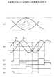
2A and 2B are explanatory diagrams of the operation of the discriminator according to the first embodiment of the present invention. FIG. 2A shows a discrimination level in an eye pattern, and a reference voltage V.1 To the first discrimination level, V1 + ΔV is the second discrimination level, V1 This is the case where −ΔV is the third identification level, and LM indicates an identification level margin.
[0043]
Reference voltage V1 Indicates the center position of the eye pattern,1 + ΔV and V1 The discrimination outputs of the received signals with the third discrimination level of -ΔV are all the same, and therefore the average values are also equal. However, with respect to the center position of the eye pattern, the reference voltage V1 Is relatively increased, the discrimination output of the received signal at the second discrimination level is likely to be different from the discrimination output of the reception signal at the first and third discrimination levels. Conversely, the reference voltage V with respect to the center position of the eye pattern1 Is relatively reduced, the identification output of the received signal at the third identification level is likely to be different from the identification output of the received signal at the first and second identification levels.
[0044]
For example, when the discrimination output of the received signal at the optimum discrimination level is shown in (B), the average value is VAVR1 It becomes. When the discrimination level rises above the optimum value, the probability that the received signal of the same level is determined to be "0" increases, for example, the discrimination output shown in (C) is obtained. The average value in this case is VAVR2 And VAVR2 <VAVR1 And can be detected by the
[0045]
From such a relationship, the average value of the discrimination output of the
[0046]
FIG. 3 is an explanatory view of a second embodiment of the present invention, wherein 11 to 13 are first to third discriminators, 14 is a reference voltage generating circuit, 15 and 16 are integrators, and 17 and 18 are exclusive. An OR circuit, 20 and 21 are voltage adders, 22 and 23 are comparators, 24 is a differential amplifier, and 25 and 26 are reference voltage power supplies. A control circuit includes the
[0047]
First to
[0048]
The exclusive OR
[0049]
FIGS. 4A and 4B are explanatory diagrams of error pulse detection according to the second embodiment of the present invention. FIG. 4A shows the identification output of the
[0050]
For example, the reference voltage V1 Rises relatively to the center position of the eye pattern, the probability that the identification output of the
[0051]
Contrary to the previous case, the reference voltage V1 Is relatively lower than the center position of the eye pattern, the probability that the discrimination output of the
[0052]
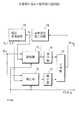
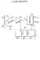
FIG. 5 is an explanatory view of the third embodiment of the present invention, wherein 31 to 33 are discriminators for a reference phase, a leading phase and a lag phase, 34 is a reference voltage generating circuit, 35 to 37 are integrators, and 38 and 39. Is a comparator, 40 to 42 are delay circuits (DL), 43 is a phase variable circuit, and 44 is an amplifier. The
[0053]
The
[0054]
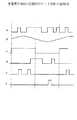
FIGS. 6A and 6B are explanatory diagrams of the discrimination phase according to the third embodiment of the present invention. FIG. 6A shows an eye pattern, FIG. 6B shows a clock signal applied to the
[0055]
Reference phase Φ1 When the phase is advanced due to, for example, temperature fluctuations of the timing recovery unit, Φ1 The error rate increases in the discrimination of the received signal in the
[0056]
Conversely, the reference phase Φ1 Is delayed from the center of the eye pattern, Φ1 The error rate in the discrimination of the received signal in the
[0057]
FIG. 7 is an explanatory diagram of the fourth embodiment of the present invention.
[0058]
Reference phase Φ1 When, for example, the leading phase becomes the leading phase from the center position of the eye pattern, as in the case described above, the discriminating output of the
[0059]
Conversely, the reference phase Φ1 Becomes the lagging phase from the center position of the eye pattern, the discriminating outputs of the reference phase and the
[0060]
FIG. 8 is an explanatory diagram of the fifth embodiment of the present invention, wherein 71 and 72 are first and second discriminators, 73 is a comparator, 74 is a reference voltage generation circuit, 75 is a voltage modulation circuit,
[0061]
The reference voltage V from the reference
[0062]
FIG. 9 is an explanatory diagram of the identification level according to the fifth embodiment of the present invention. FIG. 9A shows the reference voltage V in the
[0063]
For example, the reference voltage V1 Rises and V1 When + ΔV exceeds the range of the discrimination level margin LM, the probability that the
[0064]
Conversely, the reference voltage V1 Decreases and V1 When −ΔV exceeds the range of the discrimination level margin LM, the probability that the
[0065]
FIG. 10 is an explanatory diagram of a sixth embodiment of the present invention, wherein 81 and 82 are first and second discriminators, 83 is an exclusive OR circuit, 84 is a reference voltage generation circuit, and 85 is a voltage modulation circuit. , 86 and 87 are gate circuits, 88 and 89 are integrators, 90 is a gate control circuit, 91 and 92 are comparators, 93 is a differential amplifier, and the exclusive OR
[0066]
Input data D from the pre-stage equalizing amplifier (not shown)in (Received signal) is input to the first and
[0067]
As in the previous embodiment, the
[0068]
The
[0069]
FIG. 11 is an explanatory diagram of the gate control according to the sixth embodiment of the present invention.1 4 shows an example of an identification output of the
[0070]
Therefore, the exclusive OR output of the discrimination output of (a) and (d) from the exclusive OR
[0071]
FIG. 12 is an explanatory diagram of a seventh embodiment of the present invention. 101 and 102 are reference phase and modulation phase discriminators, 103 is a phase variable circuit, 104 is a reference voltage generation circuit, 105 and 106 are discriminators, 107 is an integration comparator, 108 is an amplifier, and 109 is a phase modulation amplifier. Input data Din Is the reference voltage V from the reference
[0072]
The
[0073]
The
[0074]
FIG. 13 is an explanatory diagram of the phase modulation according to the seventh embodiment of the present invention. FIG. 13A illustrates a case where the
[0075]
14A and 14B are explanatory diagrams of the identification phase according to the seventh embodiment of the present invention. FIG. 14A shows the identification point P in the eye pattern.1 , P2 , P3 (B) shows the reference phase Φ1 And (c) shows a frequency-modulated clock signal. The phase modulation range indicates a case where the phase modulation range is set within the range of the discrimination phase margin PM. In the eye pattern of (a), the identification point by the clock signal shown in (b) is P1 It becomes. However, the discrimination point by the clock signal shown in FIG.2 To P3 Toward P again3 To P2 It changes like an arrow toward.
[0076]
Therefore, the reference phase Φ1 Is near the center position of the eye pattern, the discrimination outputs of the
[0077]
FIGS. 15A and 15B are diagrams for explaining the synchronization of the identification output according to the seventh embodiment of the present invention. FIG.1 (B) shows the identification output of the
[0078]
Therefore, by providing
[0079]
FIG. 16 is an explanatory diagram of the eighth embodiment of the present invention. 111 and 112 are reference phase and modulation phase discriminators, 113 is a phase variable circuit, 114 is a reference voltage generation circuit, and 115 and 116 are discriminators. 117 is an exclusive OR circuit, 118 is an amplifier, 119 is a phase modulation amplifier, 120 is a gate control circuit, 121 and 122 are comparators, 123 is a differential amplifier, 126 and 127 are gate circuits, and 128 and 129 are integrators. It is.
[0080]
This embodiment corresponds to the case where the control circuit shown in FIG. 10 is applied to the control circuit of the embodiment shown in FIG. 12, and the phases of the discrimination outputs are matched by
[0081]
Therefore, the reference phase Φ1 Deviates from the vicinity of the center position of the eye pattern, the discrimination outputs of the
[0082]
FIG. 17 is an explanatory view of the ninth embodiment of the present invention, wherein 131 to 133 are first to third discriminators, 134 is a reference voltage generation circuit, 135 and 136 are discriminators, and 137 is an exclusive OR. Circuit, 138 is an amplifier, 139 is a phase modulation amplifier, 140 is a gate control circuit, 141 is a voltage modulation circuit, 142 is a comparator, 143 and 144 are integrators, 145 is a comparator, 146 and 147 are gate circuits, 148 and 148. 149 is an integrator and 150 is a phase variable circuit.
[0083]
This embodiment corresponds to a case where the embodiment shown in FIG. 8 and the embodiment shown in FIG. 16 are combined, and the description overlapping with each embodiment will be omitted. In this embodiment, the
[0084]
That is, the reference voltage V is set by the first and
[0085]
Further, a voltage control circuit is constituted by the
[0086]
FIGS. 18A and 18B are explanatory diagrams of the modulation control according to the ninth embodiment of the present invention. FIGS. 18A and 18B show an identification range based on a modulation voltage and a modulation phase for an eye pattern. In (A), the identification margin is Ma , The identification margin Ma So that the reference voltage V1 Is 2ΔVa And the reference phase Φ1 Is 2ΔΦa Modulation in the range That is, V1 ± ΔVa Is applied as a discrimination level of the
[0087]
Therefore, the reference voltage V1 Modulation range and reference phase Φ1 Is the discrimination margin Ma In the same manner as in the above-described embodiments, the reference voltage V1 And reference phase Φ1 Can be automatically optimized.
[0088]
The eye pattern opens greatly when the received signal power is large, and conversely when the received signal power is small. Therefore, in an optical communication system, the received light power is detected, and in a general communication system including the optical communication system, an AGC voltage or the like in an AGC amplifier is detected, and a reference voltage V is detected.1 And reference phase Φ1 Can be controlled.
[0089]
That is, FIG. 18A shows that the received signal power is PW1 Assuming that the eye pattern at the time of1 Is 2ΔVa And the reference phase Φ1 Is 2ΔΦa The degree of modulation is controlled so as to fall within the range. Also, the received signal power becomes smaller and the PW2 Then, as shown in (B), the opening of the eye pattern becomes smaller. In that case, the reference voltage V1 Is 2ΔVb And the reference phase Φ1 Is 2ΔΦb Is controlled so as to fall within the range ofb So that the reference voltage V1 And reference phase Φ1 Control. The modulation degree in that case can be controlled by adding the above-mentioned detection signal of the received signal power to the
[0090]
FIG. 19 is an explanatory diagram of the tenth embodiment of the present invention, wherein 151 to 153 are first to third discriminators, 154 is a reference voltage generation circuit, 155 and 156 are discriminators, and 157 is an exclusive OR. Circuit, 158 is an amplifier, 159 is a phase modulation amplifier, 160 is a gate control circuit, 161 is a voltage modulation circuit, 162 is a comparator, 163 is an exclusive OR circuit, 164 is a gate control circuit, 165 is a comparator, 166 167, 171 and 172 are gate circuits, 168, 169, 173 and 174 are integrators and 170 is a phase variable circuit.
[0091]
This embodiment corresponds to a configuration in which the embodiment shown in FIG. 10 and the embodiment shown in FIG. 16 are combined, and the first to
[0092]
FIG. 20 is an explanatory view of the eleventh embodiment of the present invention.
[0093]
In this embodiment, the output signal of the
[0094]
Further, the
[0095]
That is, V1 + ΔV to the integrator 203,1 The comparison output during the period of −ΔV is distributed to the
[0096]
FIGS. 21A and 21B are diagrams for explaining an identification operation according to the eleventh embodiment of the present invention. FIG. 21A shows an identification point in an eye pattern, and FIG.1 And the modulation signal F applied to the
[0097]
(C) to (f) show an example of the gate control signal, and (c) shows the reference voltage V.1 , A gate control signal that opens the
[0098]
In the case of the gate control signals shown in (c) to (f), the output signals of the exclusive OR circuit 187 are respectively distributed to the integrators.1 + ΔV period and V1 The
[0099]
In each of the above embodiments, the received signal power is detected and the reference voltage V1 Of modulation and reference phase Φ1 One or both of the modulation degrees can be controlled. In this case, as a means for detecting the received signal power, a configuration for detecting the received optical power or a configuration for detecting the AGC voltage of the AGC amplifier can be applied in the optical communication system. Also, when the reception signal disconnection is detected, the reference voltage V1 And reference phase Φ1 May be provided to stop the control of. Such a configuration can be realized by adding a detection signal of a known reception signal disconnection detection circuit to a reference voltage generation circuit or a phase variable circuit. Reference voltage V1 Or reference phase Φ1 Is set so as to exceed the discrimination margin, and the reference voltage V is set based on the error rate curve.1 Or reference phase Φ1 Can be controlled.
[0100]
【The invention's effect】
As described above, according to the present invention, the reference voltage V1 And reference phase Φ1 The reference voltage V1 Is the discrimination level, and the reference phase Φ1 To the reference voltage V1 Output when the voltage shifted to + ΔV and −ΔV is used as the identification level, or the reference phase Φ1 The reference voltage V is based on the difference between the discrimination output when the phase shifted to + ΔΦ and −ΔΦ is used as the discrimination phase.1 Or reference phase Φ1 The reference voltage V is adjusted without adjustment.1 Or reference phase Φ1 There is an advantage that can be optimized. Reference voltage V due to aging, temperature change, power supply voltage change, etc.1 And the reference phase Φ1 Will be controlled so as to be automatically corrected even when a change in1 And reference phase Φ1 There is an advantage that can be obtained.
[0101]
Reference voltage V1 Or reference phase Φ1 Is frequency-modulated, the number of discriminators can be reduced. Reference voltage V1 And reference phase Φ1 By giving the same modulation frequency to the above and providing a phase difference of 90 degrees, an identification point of a locus of a circle or an ellipse can be obtained with respect to the eye pattern. Therefore, even when the distortion of the eye pattern is large, Reference voltage V1 And reference phase Φ1 There is an advantage that can be controlled.
[0102]
Based on various conditions such as input signal power, the reference voltage V1 ΔV and the reference phase Φ1 By controlling the magnitude of ΔΦ with respect to or the degree of modulation when frequency modulation is performed, it is possible to control the optimal identification level and the optimal identification phase according to the range of the identification margin corresponding to the size of the eye pattern opening. There are advantages.
[Brief description of the drawings]
FIG. 1 is an explanatory diagram of a first embodiment of the present invention.
FIG. 2 is an explanatory diagram of an operation of the discriminator according to the first embodiment of the present invention.
FIG. 3 is an explanatory diagram of a second embodiment of the present invention.
FIG. 4 is an explanatory diagram of error pulse detection according to a second embodiment of the present invention.
FIG. 5 is an explanatory diagram of a third embodiment of the present invention.
FIG. 6 is an explanatory diagram of an identification phase according to a third embodiment of the present invention.
FIG. 7 is an explanatory diagram of a fourth embodiment of the present invention.
FIG. 8 is an explanatory diagram of a fifth embodiment of the present invention.
FIG. 9 is an explanatory diagram of an identification level according to a fifth embodiment of the present invention.
FIG. 10 is an explanatory diagram of a sixth embodiment of the present invention.
FIG. 11 is an explanatory diagram of gate control according to a sixth embodiment of the present invention.
FIG. 12 is an explanatory diagram of a seventh embodiment of the present invention.
FIG. 13 is an explanatory diagram of phase modulation according to a seventh embodiment of the present invention.
FIG. 14 is an explanatory diagram of an identification phase according to a seventh embodiment of the present invention.
FIG. 15 is an explanatory diagram of synchronization of identification output according to the seventh embodiment of the present invention.
FIG. 16 is an explanatory diagram of an eighth embodiment of the present invention.
FIG. 17 is an explanatory diagram of a ninth embodiment of the present invention.
FIG. 18 is an explanatory diagram of modulation control according to a ninth embodiment of the present invention.
FIG. 19 is an explanatory diagram of a tenth embodiment of the present invention.
FIG. 20 is an explanatory diagram of an eleventh embodiment of the present invention.
FIG. 21 is an explanatory diagram of an identification operation according to an eleventh embodiment of the present invention.
FIG. 22 is a schematic explanatory diagram of an optical receiver.
FIG. 23 is an explanatory diagram of an identification operation.
[Explanation of symbols]
1 First discriminator
2 Second classifier
3 Third classifier
4 Reference voltage generation circuit
5-7 integrator
8,9 comparator
10,11 voltage adder
Claims (8)
Translated fromJapanese基準電圧を第1の識別レベルとして前記受信信号を識別する第1の識別器と、
前記基準電圧を前記受信信号の伝送速度に比較して小さい速度で振幅変調した電圧を第2の識別レベルとして前記受信信号を識別する第2の識別器と、
前記第1の識別器の識別出力の平均値と、前記第2の識別器の識別出力の平均値とが等しくなるように前記基準電圧を制御し、且つ前記基準電圧の振幅変調の変調度を前記受信信号パワーに基づいて制御する制御回路と
を備えたことを特徴とする識別回路。In an identification circuit for identifying a received signal by an identification level and at an identification phase,
A first identifier for identifying the received signal using a reference voltage as a first identification level;
A second discriminator that identifies the received signal as a voltage obtained byamplitude- modulating the reference voltage at a small speed compared to the transmission speed of the received signal as a second identification level;
The reference voltage is controlled sothat the average value of the identification output of the first classifier and the average value of the identification output of the second classifier become equal, and the modulation degree of the amplitude modulation of the reference voltage is adjusted. A control circuitfor controlling based on the received signal power .
基準電圧を第1の識別レベルとして前記受信信号を識別する第1の識別器と、
前記基準電圧を前記受信信号の伝送速度に比較して小さい速度で振幅変調した電圧を第2の識別レベルとして前記受信信号を識別する第2の識別器と、
前記第1の識別器の識別出力と前記第2の識別器の識別出力との排他的論理和出力を、前記基準電圧の変調周期に従い、前記第2の識別レベルと前記第1の識別レベルとの大小関係に応じて選択してそれぞれの平均値を求め、該平均値に従って前記基準電圧を制御し、且つ前記基準電圧の振幅変調の変調度を前記受信信号のパワーに基づいて制御する制御回路と
を備えたことを特徴とする識別回路。In identifying identification circuit In the reception signal and the identification phaseby the identification level,
A first identifier for identifying the received signal using a reference voltage as a first identification level;
A second discriminator that identifies the received signal as a voltage obtained byamplitude- modulating the reference voltage at a small speed compared to the transmission speed of the received signal as a second identification level;
An exclusive-OR output of the identification output of the first classifier and the identification output of the second classifier is calculatedaccording to the modulation cycleof the reference voltage,the second identification level, the first identification level, A control circuit for selecting the average value according to the magnitude relation of the control signal, obtaining the average value, controlling the reference voltage according to the average value, and controlling the modulation degree of the amplitude modulation of the reference voltage based on the power of the reception signal. And an identification circuit comprising:
基準位相を識別位相として前記受信信号を識別する基準位相の識別器と、
前記基準位相を周波数変調した識別位相により前記受信信号を識別する変調位相の識別器と、
前記基準位相の識別器の識別出力と前記変調位相の識別器の識別出力との排他的論理和出力を、前記基準位相の変調周期に従い、前記基準位相と前記変調位相との大小関係に応じて選択してそれぞれの平均値を求め、該平均値に従って前記基準位相を制御し、且つ前記変調位相の変調度を前記受信信号パワーの検出信号に基づいて制御する制御回路と
を備えたことを特徴とする識別回路。In identifying identification circuit In the reception signal and the identification phaseby the identification level,
A reference phase identifier for identifying the received signal as a reference phase as an identification phase,
A discriminator of a modulation phase for discriminating the received signal by a discrimination phase obtained byfrequency- modulating the reference phase,
The exclusive-OR output of the discrimination output of the discrimination device of the reference phase and the discrimination output of the discrimination device of themodulation phase, according to the modulation cycle of the reference phase, according to the magnitude relationship between the reference phase and the modulation phase. And a control circuitfor controlling the reference phase according to the average value and controlling the degree of modulation of the modulation phase based on the detection signal of the received signal power. Identification circuit.
基準電圧を第1の識別レベルとし、且つ基準位相を識別位相として前記受信信号を識別する第1の識別器と、
前記基準電圧を振幅変調した電圧を第2の識別レベルとし、且つ前記基準位相を識別位相として前記受信信号を識別する第2の識別器と、
前記基準電圧を第1の識別レベルとし、前記基準位相を周波数変調した位相を識別位相として前記受信信号を識別する第3の識別器と、
前記第1の識別器の識別出力と前記第2の識別器の識別出力との平均値が等しくなるように前記基準電圧を制御する電圧制御回路と、
前記第1の識別器の識別出力と前記第3の識別器の識別出力との排他的論理和出力を、前記基準位相の変調周期に従い、前記基準位相と前記変調位相との大小関係に応じて選択してそれぞれの平均値を求め、該平均値に従って前記基準位相を制御し、且つ前記変調位相の変調度を前記受信信号パワーの検出信号に基づいて制御する位相制御回路と
を備えたことを特徴とする識別回路。In an identification circuit for identifying a received signal by an identification level and at an identification phase,
A first discriminator that identifies the received signal using a reference voltage as a first identification level and a reference phase as an identification phase;
A second discriminator that sets the voltage obtained by amplitude-modulating the reference voltage as a second identification level, and identifies the received signal using the reference phase as an identification phase;
A third identification unit that identifies the received signal as an identification phase using the reference voltage as a first identification level and a phase obtained by frequency-modulating the reference phase as an identification phase;
A voltage control circuit that controls the reference voltage so that an average value of the identification output of the first classifier and the identification output of the second classifier is equal;
The exclusive OR output of the identification output of the first classifier and the identification output of the third classifier is calculated according to the modulation cycle of the reference phase, and according to the magnitude relationship between the reference phase and the modulation phase. A phase control circuit that selects and calculates respective average values, controls the reference phase according to the average values, and controls the degree of modulation of the modulation phase based on the detection signal of the received signal power. An identification circuit, comprising:
基準電圧を第1の識別レベルとし、且つ基準位相を識別位相として前記受信信号を識別する第1の識別器と、
前記基準電圧を振幅変調した電圧を第2の識別レベルとし、且つ前記基準位相を識別位相として前記受信信号を識別する第2の識別器と、
前記基準電圧を第1の識別レベルとし、前記基準位相を周波数変調した位相を識別位相として前記受信信号を識別する第3の識別器と、
前記第1の識別器の識別出力と前記第2の識別器の識別出力との排他的論理和出力を、前記基準電圧の変調周期に従い、前記第1の識別レベルに対する前記第2の識別レベルの極性に応じて選択してそれぞれの平均値を求め、該平均値に従って前記基準位相を制御し、且つ前記基準電圧の振幅変調の変調度を前記受信信号のパワーに基づいて制御する電圧制御回路と、
前記第1の識別器の識別出力と前記第3の識別器の識別出力との排他的論理和出力を、前記基準位相の変調周期に従い、前記基準位相と前記変調位相との大小関係に応じて選択して平均値を求め、該平均値に従って前記基準位相を制御し、且つ前記変調位相の変調度を前記受信信号のパワーに基づいて制御する位相制御回路と
を備えたことを特徴とする識別回路。In identifying identification circuit In the reception signal and the identification phaseby the identification level,
Afirst discriminator that identifies the received signal using a reference voltage as afirst identification level and a reference phase as an identification phase;
Asecond discriminator thatsets the voltage obtained byamplitude- modulating the reference voltage as asecond identification level, and identifies the received signal using the reference phase as an identification phase;
A third identification unit that identifies the received signal as an identification phase usingthe reference voltage as afirst identification level and a phase obtained by frequency-modulating the reference phase as an identification phase;
Anexclusive-OR output of the identification output of the first classifier and the identification output of the second classifier iscalculated according to a modulation period of the reference voltage, based on the second identification level with respect to the first identification level. A voltage control circuitfor selecting an average value by selecting according to the polarity, controlling the reference phase according to the average value, and controlling the modulation degree of amplitude modulation of the reference voltage based on the power of the reception signal; and ,
The exclusive OR output of the identification output of the first classifier and the identification output of the third classifier is calculatedaccording to the modulation cycleof the reference phase, and according to the magnitude relationship between the reference phase and the modulation phase. A phase control circuitfor selecting the average value, controlling the reference phase according to the average value, and controlling the degree of modulation of the modulation phase based on the power of the received signal. circuit.
基準電圧を第1の識別レベルとし、且つ基準位相を識別位相として前記受信信号を識別する第1の識別器と、
前記基準電圧を振幅変調した電圧を第2の識別レベルとし、且つ前記基準位相を前記基準電圧の変調周波数と同一で且つπ/2の位相差の周波数で変調した位相を識別位相として前記受信信号を識別する第2の識別器と、
前記第1の識別器と前記第2の識別器との識別出力をそれぞれ同一位相とする為の同一位相で動作する第4及び第5の識別器と、
該第4及び第5の識別器の識別出力の排他的論理和を求める排他的論理和回路と、
該排他的論理和回路の出力を、前記基準電圧の変調周期に従い、前記第1の識別レベルに対する前記第2の識別レベルの極性に応じて選択してそれぞれ平均値を求め、該平均値に従って前記基準電圧を制御し、且つ前記基準電圧の振幅変調の変調度を前記受信信号のパワーに基づいて制御する電圧制御回路と、
前記排他的論理和回路の出力を、前記基準位相の変調周期に従い、前記基準位相と前記変調位相との大小関係に応じて選択してそれぞれの平均値を求め、該平均値に従って前記基準位相を制御し、且つ前記変調位相の変調度を前記受信信号のパワーに基づいて制御する位相制御回路と
を備えたことを特徴とする識別回路。In an identification circuit for identifying a received signal by an identification level and at an identification phase,
A first discriminator that identifies the received signal using a reference voltage as a first identification level and a reference phase as an identification phase ;
The received signal is defined as a voltage obtained by amplitude-modulating the reference voltage as a second identification level, and a phase obtained by modulating the reference phase at a frequency equal to the modulation frequency of the reference voltage and having a phase difference of π / 2 as an identification phase. A second classifier for identifying
Fourth and fifth classifiers operating in the same phase to make the classification outputs of the first classifier and the second classifier the same phase, respectively;
An exclusive-OR circuit for obtaining an exclusive-OR of the identification outputs of the fourth and fifth classifiers;
The outputs of the exclusive OR circuits are selected according to the modulation period of the reference voltage and according to the polarity of the second identification level with respect to the first identification level, and the respective average values are obtained. A voltage control circuit that controls a reference voltage and controls a modulation degree of the amplitude modulation of the reference voltage based on a power of the reception signal.
The output of the exclusive OR circuit is selected in accordance with the modulation period of the reference phase, according to the magnitude relationship between the reference phase and the modulation phase, and the respective average values are obtained.The reference phase is calculated according to the average value. A phase control circuit for controlling and controlling the degree of modulation of the modulation phase based on the power of the received signal.
An identification circuit comprising:
Priority Applications (2)
| Application Number | Priority Date | Filing Date | Title |
|---|---|---|---|
| JP06121095AJP3551393B2 (en) | 1995-03-20 | 1995-03-20 | Identification circuit |
| US08/618,941US5736875A (en) | 1995-03-20 | 1996-03-20 | Discrimination circuit capable of automatically optimizing discrimination level and discrimination phase |
Applications Claiming Priority (1)
| Application Number | Priority Date | Filing Date | Title |
|---|---|---|---|
| JP06121095AJP3551393B2 (en) | 1995-03-20 | 1995-03-20 | Identification circuit |
Publications (2)
| Publication Number | Publication Date |
|---|---|
| JPH08265375A JPH08265375A (en) | 1996-10-11 |
| JP3551393B2true JP3551393B2 (en) | 2004-08-04 |
Family
ID=13164617
Family Applications (1)
| Application Number | Title | Priority Date | Filing Date |
|---|---|---|---|
| JP06121095AExpired - Fee RelatedJP3551393B2 (en) | 1995-03-20 | 1995-03-20 | Identification circuit |
Country Status (2)
| Country | Link |
|---|---|
| US (1) | US5736875A (en) |
| JP (1) | JP3551393B2 (en) |
Families Citing this family (28)
| Publication number | Priority date | Publication date | Assignee | Title |
|---|---|---|---|---|
| JP3863265B2 (en)* | 1997-10-16 | 2006-12-27 | 富士通株式会社 | Optical receiver and clock extraction circuit |
| FR2772923B1 (en)* | 1997-12-23 | 2000-03-17 | Sextant Avionique | ELECTRONIC ELECTRICAL VOLTAGE MONITORING CIRCUIT |
| JP3221401B2 (en) | 1998-06-15 | 2001-10-22 | 日本電気株式会社 | Optical signal monitoring method and apparatus |
| US6188737B1 (en) | 1999-11-24 | 2001-02-13 | Nortel Networks Limited | Method and apparatus for regenerating data |
| CA2328251C (en)* | 1999-12-15 | 2004-05-25 | Nec Corporation | Automatic identification level control circuit, identification level control method, automatic identification phase control circuit, identification phase control method, optical receiver, and optical communication system |
| DE10052279A1 (en)* | 2000-10-20 | 2002-04-25 | Alcatel Sa | Fast eye monitor and receiver with fast eye monitor |
| EP1282256B1 (en)* | 2001-08-01 | 2006-10-04 | Alcatel | Measurement of the eye-opening of a signal |
| JP3652995B2 (en) | 2001-03-16 | 2005-05-25 | 日本電気株式会社 | Identification voltage control circuit, identification voltage control method, optical receiver, identification voltage control program for clock data recovery circuit |
| JP4828730B2 (en)* | 2001-07-05 | 2011-11-30 | 富士通株式会社 | Transmission equipment |
| JP3856101B2 (en) | 2001-09-03 | 2006-12-13 | 日本電気株式会社 | Optical receiver having reception waveform shaping function |
| JP3839830B2 (en)* | 2002-12-05 | 2006-11-01 | 富士通株式会社 | Digital signal receiving apparatus, optical transmission apparatus having the digital signal receiving apparatus, and discrimination point control method |
| US20050149791A1 (en)* | 2002-12-05 | 2005-07-07 | Fujitsu Limited | Digital signal receiving apparatus, an optical transmission apparatus therewith, and a discriminating point control method |
| ATE363781T1 (en)* | 2002-12-30 | 2007-06-15 | Alcatel Lucent | DEVICE AND METHOD FOR EYE PATTERN MEASURING A DIGITAL SIGNAL |
| WO2004088912A1 (en)* | 2003-03-31 | 2004-10-14 | Hitachi, Ltd. | Data reproducing circuit and data reproducing method |
| DE10331829B4 (en)* | 2003-07-14 | 2009-04-16 | Qimonda Ag | Method and device for generating a reference voltage |
| DE10350261B4 (en)* | 2003-10-28 | 2006-04-20 | Infineon Technologies Ag | Method and apparatus for adjusting thresholds in electronic signal processing equipment |
| JP4299179B2 (en) | 2004-03-31 | 2009-07-22 | 富士通株式会社 | Discrimination phase margin monitor circuit, transmission / reception device, and communication system |
| US7386041B2 (en)* | 2005-02-24 | 2008-06-10 | Agilent Technologies, Inc. | Method for normalization of an eye diagram and selection of sampling parameters for a receiver |
| KR100782323B1 (en)* | 2006-10-16 | 2007-12-06 | 삼성전자주식회사 | Semiconductor device and method capable of reducing noise of output driver |
| TWI333740B (en)* | 2007-02-14 | 2010-11-21 | Princeton Technology Corp | Baseline wandering correcting apparatus and the related method |
| US7825697B2 (en)* | 2008-02-29 | 2010-11-02 | Faraday Technology Corp. | Signal detection circuit with deglitch and method thereof |
| EP2375621A4 (en)* | 2008-12-11 | 2012-05-02 | Fujitsu Ltd | RECEIVING DEVICE, TRANSMISSION DEVICE, AND TRANSMISSION METHOD |
| JP2010161692A (en)* | 2009-01-09 | 2010-07-22 | Nikon Systems Inc | Data transfer apparatus and camera |
| JP5738724B2 (en)* | 2011-09-07 | 2015-06-24 | ラピスセミコンダクタ株式会社 | Trimming circuit, system, determination program, confirmation method, and determination method |
| JP2013219641A (en)* | 2012-04-11 | 2013-10-24 | Mitsubishi Electric Corp | Data transmission device |
| JP2014230043A (en)* | 2013-05-21 | 2014-12-08 | 富士通オプティカルコンポーネンツ株式会社 | Optical receiver and identification level control method |
| DE102013214870A1 (en)* | 2013-07-30 | 2015-02-05 | Robert Bosch Gmbh | Subscriber station for a bus system and method for improving the error robustness of a subscriber station of a bus system |
| US10446255B2 (en)* | 2016-06-13 | 2019-10-15 | International Business Machines Corporation | Reference voltage calibration in memory during runtime |
Family Cites Families (6)
| Publication number | Priority date | Publication date | Assignee | Title |
|---|---|---|---|---|
| US3851259A (en)* | 1973-03-30 | 1974-11-26 | Bendix Corp | Deadzone circuit |
| US3936755A (en)* | 1974-07-19 | 1976-02-03 | Rca Corporation | Proximity switch circuit |
| US4823360A (en)* | 1988-02-12 | 1989-04-18 | Northern Telecom Limited | Binary data regenerator with adaptive threshold level |
| JP2530904B2 (en)* | 1988-02-22 | 1996-09-04 | 富士通株式会社 | Optimal discrimination level control method |
| US5373400A (en)* | 1993-12-01 | 1994-12-13 | Analog Devices, Inc. | Dynamic threshold updating circuit for a maximum likelihood detector using both positive and negative comparators |
| KR0139981B1 (en)* | 1995-06-12 | 1998-07-15 | 김광호 | Hysteresis system having the uniform threshold voltage |
- 1995
- 1995-03-20JPJP06121095Apatent/JP3551393B2/ennot_activeExpired - Fee Related
- 1996
- 1996-03-20USUS08/618,941patent/US5736875A/ennot_activeExpired - Lifetime
Also Published As
| Publication number | Publication date |
|---|---|
| US5736875A (en) | 1998-04-07 |
| JPH08265375A (en) | 1996-10-11 |
Similar Documents
| Publication | Publication Date | Title |
|---|---|---|
| JP3551393B2 (en) | Identification circuit | |
| US6496552B2 (en) | Timing circuit | |
| US6188738B1 (en) | Clock extraction circuit | |
| JPH0586096B2 (en) | ||
| US20030043440A1 (en) | Receiver and receiving method capable of detecting an eye aperture size formed by reception data signals | |
| US8208596B2 (en) | System and method for implementing a dual-mode PLL to support a data transmission procedure | |
| US6882944B2 (en) | Threshold setting apparatus for adjustably setting a threshold for use in identifying serial data from a baseband signal | |
| JP2001177397A (en) | Phase frequency synchronizing circuit and light receiving circuit | |
| JP3569022B2 (en) | Automatic identification threshold control device | |
| US6959061B1 (en) | Phase comparator circuit | |
| US4320527A (en) | Bit synchronizing system for pulse signal transmission | |
| WO2021240695A1 (en) | Optical reception device and clock synchronization method | |
| JP3589836B2 (en) | Optical receiver | |
| EP0840317B1 (en) | Digital signal reproduction | |
| JP4137120B2 (en) | Preamplifier circuit, clock switching circuit, and optical receiver using the same | |
| JP4696254B2 (en) | Lock detection and operation alarm detection circuit | |
| JP2001186199A (en) | Transmission speed detection circuit and optical receiver | |
| EP0659000A2 (en) | Threshold setting and decision circuit | |
| JP3304154B2 (en) | Data waveform shaping circuit | |
| JP2004336200A (en) | Burst signal start detection circuit, optical receiver, and optical transmission system | |
| JP3907318B2 (en) | Transmission waveform conversion receiving circuit and transmission waveform conversion receiving method | |
| JPH0740697B2 (en) | Identification circuit | |
| JPH0736500B2 (en) | AGC control method | |
| JPH06224949A (en) | Data waveform shaping circuit | |
| JPH114264A (en) | Digital signal identification circuit |
Legal Events
| Date | Code | Title | Description |
|---|---|---|---|
| A02 | Decision of refusal | Free format text:JAPANESE INTERMEDIATE CODE: A02 Effective date:20031224 | |
| A521 | Request for written amendment filed | Free format text:JAPANESE INTERMEDIATE CODE: A523 Effective date:20040220 | |
| A911 | Transfer to examiner for re-examination before appeal (zenchi) | Free format text:JAPANESE INTERMEDIATE CODE: A911 Effective date:20040225 | |
| TRDD | Decision of grant or rejection written | ||
| A01 | Written decision to grant a patent or to grant a registration (utility model) | Free format text:JAPANESE INTERMEDIATE CODE: A01 Effective date:20040323 | |
| A61 | First payment of annual fees (during grant procedure) | Free format text:JAPANESE INTERMEDIATE CODE: A61 Effective date:20040416 | |
| R150 | Certificate of patent or registration of utility model | Free format text:JAPANESE INTERMEDIATE CODE: R150 | |
| FPAY | Renewal fee payment (event date is renewal date of database) | Free format text:PAYMENT UNTIL: 20080514 Year of fee payment:4 | |
| FPAY | Renewal fee payment (event date is renewal date of database) | Free format text:PAYMENT UNTIL: 20090514 Year of fee payment:5 | |
| FPAY | Renewal fee payment (event date is renewal date of database) | Free format text:PAYMENT UNTIL: 20090514 Year of fee payment:5 | |
| FPAY | Renewal fee payment (event date is renewal date of database) | Free format text:PAYMENT UNTIL: 20100514 Year of fee payment:6 | |
| FPAY | Renewal fee payment (event date is renewal date of database) | Free format text:PAYMENT UNTIL: 20100514 Year of fee payment:6 | |
| FPAY | Renewal fee payment (event date is renewal date of database) | Free format text:PAYMENT UNTIL: 20110514 Year of fee payment:7 | |
| FPAY | Renewal fee payment (event date is renewal date of database) | Free format text:PAYMENT UNTIL: 20120514 Year of fee payment:8 | |
| FPAY | Renewal fee payment (event date is renewal date of database) | Free format text:PAYMENT UNTIL: 20130514 Year of fee payment:9 | |
| LAPS | Cancellation because of no payment of annual fees |