JP3549208B2 - Integrated redistribution routing conductors, solder vipes and methods of forming structures formed thereby - Google Patents
Integrated redistribution routing conductors, solder vipes and methods of forming structures formed therebyDownload PDFInfo
- Publication number
- JP3549208B2 JP3549208B2JP53031796AJP53031796AJP3549208B2JP 3549208 B2JP3549208 B2JP 3549208B2JP 53031796 AJP53031796 AJP 53031796AJP 53031796 AJP53031796 AJP 53031796AJP 3549208 B2JP3549208 B2JP 3549208B2
- Authority
- JP
- Japan
- Prior art keywords
- solder
- bump
- metal layer
- under
- layer
- Prior art date
- Legal status (The legal status is an assumption and is not a legal conclusion. Google has not performed a legal analysis and makes no representation as to the accuracy of the status listed.)
- Expired - Lifetime
Links
- 229910000679solderInorganic materials0.000titleclaimsdescription331
- 238000000034methodMethods0.000titleclaimsdescription34
- 239000004020conductorSubstances0.000titleclaimsdescription25
- 229910052751metalInorganic materials0.000claimsdescription117
- 239000002184metalSubstances0.000claimsdescription117
- 239000000758substrateSubstances0.000claimsdescription42
- 238000004377microelectronicMethods0.000claimsdescription38
- 229910000765intermetallicInorganic materials0.000claimsdescription14
- 238000010276constructionMethods0.000claims1
- 238000004519manufacturing processMethods0.000description11
- VYZAMTAEIAYCRO-UHFFFAOYSA-NChromiumChemical compound[Cr]VYZAMTAEIAYCRO-UHFFFAOYSA-N0.000description10
- 229910052719titaniumInorganic materials0.000description10
- 239000010936titaniumSubstances0.000description10
- RTAQQCXQSZGOHL-UHFFFAOYSA-NTitaniumChemical compound[Ti]RTAQQCXQSZGOHL-UHFFFAOYSA-N0.000description9
- 229910052804chromiumInorganic materials0.000description9
- 239000011651chromiumSubstances0.000description9
- RYGMFSIKBFXOCR-UHFFFAOYSA-NCopperChemical compound[Cu]RYGMFSIKBFXOCR-UHFFFAOYSA-N0.000description8
- 229910052802copperInorganic materials0.000description8
- 239000010949copperSubstances0.000description8
- 239000000463materialSubstances0.000description8
- 238000009713electroplatingMethods0.000description7
- 239000007788liquidSubstances0.000description7
- 238000005272metallurgyMethods0.000description7
- ATJFFYVFTNAWJD-UHFFFAOYSA-NTinChemical compound[Sn]ATJFFYVFTNAWJD-UHFFFAOYSA-N0.000description6
- 230000004888barrier functionEffects0.000description6
- 238000005516engineering processMethods0.000description3
- 238000002161passivationMethods0.000description3
- 238000007747platingMethods0.000description3
- VYPSYNLAJGMNEJ-UHFFFAOYSA-NSilicium dioxideChemical compoundO=[Si]=OVYPSYNLAJGMNEJ-UHFFFAOYSA-N0.000description2
- 229910045601alloyInorganic materials0.000description2
- 239000000956alloySubstances0.000description2
- 230000015572biosynthetic processEffects0.000description2
- 238000010438heat treatmentMethods0.000description2
- 239000004005microsphereSubstances0.000description2
- 238000007650screen-printingMethods0.000description2
- 239000004065semiconductorSubstances0.000description2
- 229910017150AlTiInorganic materials0.000description1
- 229910018082Cu3SnInorganic materials0.000description1
- GYHNNYVSQQEPJS-UHFFFAOYSA-NGalliumChemical compound[Ga]GYHNNYVSQQEPJS-UHFFFAOYSA-N0.000description1
- 239000004642PolyimideSubstances0.000description1
- 229910052581Si3N4Inorganic materials0.000description1
- 238000002679ablationMethods0.000description1
- 239000000853adhesiveSubstances0.000description1
- 230000001070adhesive effectEffects0.000description1
- 229910052782aluminiumInorganic materials0.000description1
- XAGFODPZIPBFFR-UHFFFAOYSA-NaluminiumChemical compound[Al]XAGFODPZIPBFFR-UHFFFAOYSA-N0.000description1
- 230000009286beneficial effectEffects0.000description1
- 239000003990capacitorSubstances0.000description1
- 239000002131composite materialSubstances0.000description1
- 239000000470constituentSubstances0.000description1
- 238000001816coolingMethods0.000description1
- 238000000151depositionMethods0.000description1
- 230000008021depositionEffects0.000description1
- 229910003460diamondInorganic materials0.000description1
- 239000010432diamondSubstances0.000description1
- 239000003989dielectric materialSubstances0.000description1
- 238000007772electroless platingMethods0.000description1
- 238000004100electronic packagingMethods0.000description1
- 229910052733galliumInorganic materials0.000description1
- 229910052738indiumInorganic materials0.000description1
- APFVFJFRJDLVQX-UHFFFAOYSA-Nindium atomChemical compound[In]APFVFJFRJDLVQX-UHFFFAOYSA-N0.000description1
- 230000010354integrationEffects0.000description1
- 230000000873masking effectEffects0.000description1
- 238000001465metallisationMethods0.000description1
- 150000002739metalsChemical class0.000description1
- 238000000059patterningMethods0.000description1
- 238000000206photolithographyMethods0.000description1
- 229920002120photoresistant polymerPolymers0.000description1
- 229920001721polyimidePolymers0.000description1
- 238000003825pressingMethods0.000description1
- 229910052710siliconInorganic materials0.000description1
- 239000010703siliconSubstances0.000description1
- HBMJWWWQQXIZIP-UHFFFAOYSA-Nsilicon carbideChemical compound[Si+]#[C-]HBMJWWWQQXIZIP-UHFFFAOYSA-N0.000description1
- 229910010271silicon carbideInorganic materials0.000description1
- 235000012239silicon dioxideNutrition0.000description1
- 239000000377silicon dioxideSubstances0.000description1
- HQVNEWCFYHHQES-UHFFFAOYSA-Nsilicon nitrideChemical compoundN12[Si]34N5[Si]62N3[Si]51N64HQVNEWCFYHHQES-UHFFFAOYSA-N0.000description1
- 238000003892spreadingMethods0.000description1
- 239000000126substanceSubstances0.000description1
- 150000003608titaniumChemical class0.000description1
- 238000007740vapor depositionMethods0.000description1
Images


Classifications
- H—ELECTRICITY
- H01—ELECTRIC ELEMENTS
- H01L—SEMICONDUCTOR DEVICES NOT COVERED BY CLASS H10
- H01L24/00—Arrangements for connecting or disconnecting semiconductor or solid-state bodies; Methods or apparatus related thereto
- H01L24/01—Means for bonding being attached to, or being formed on, the surface to be connected, e.g. chip-to-package, die-attach, "first-level" interconnects; Manufacturing methods related thereto
- H01L24/10—Bump connectors ; Manufacturing methods related thereto
- H01L24/12—Structure, shape, material or disposition of the bump connectors prior to the connecting process
- H01L24/13—Structure, shape, material or disposition of the bump connectors prior to the connecting process of an individual bump connector
- H—ELECTRICITY
- H01—ELECTRIC ELEMENTS
- H01L—SEMICONDUCTOR DEVICES NOT COVERED BY CLASS H10
- H01L24/00—Arrangements for connecting or disconnecting semiconductor or solid-state bodies; Methods or apparatus related thereto
- H01L24/01—Means for bonding being attached to, or being formed on, the surface to be connected, e.g. chip-to-package, die-attach, "first-level" interconnects; Manufacturing methods related thereto
- H01L24/10—Bump connectors ; Manufacturing methods related thereto
- H01L24/11—Manufacturing methods
- H—ELECTRICITY
- H01—ELECTRIC ELEMENTS
- H01L—SEMICONDUCTOR DEVICES NOT COVERED BY CLASS H10
- H01L2224/00—Indexing scheme for arrangements for connecting or disconnecting semiconductor or solid-state bodies and methods related thereto as covered by H01L24/00
- H01L2224/01—Means for bonding being attached to, or being formed on, the surface to be connected, e.g. chip-to-package, die-attach, "first-level" interconnects; Manufacturing methods related thereto
- H01L2224/02—Bonding areas; Manufacturing methods related thereto
- H01L2224/023—Redistribution layers [RDL] for bonding areas
- H01L2224/0231—Manufacturing methods of the redistribution layers
- H—ELECTRICITY
- H01—ELECTRIC ELEMENTS
- H01L—SEMICONDUCTOR DEVICES NOT COVERED BY CLASS H10
- H01L2224/00—Indexing scheme for arrangements for connecting or disconnecting semiconductor or solid-state bodies and methods related thereto as covered by H01L24/00
- H01L2224/01—Means for bonding being attached to, or being formed on, the surface to be connected, e.g. chip-to-package, die-attach, "first-level" interconnects; Manufacturing methods related thereto
- H01L2224/02—Bonding areas; Manufacturing methods related thereto
- H01L2224/04—Structure, shape, material or disposition of the bonding areas prior to the connecting process
- H01L2224/0401—Bonding areas specifically adapted for bump connectors, e.g. under bump metallisation [UBM]
- H—ELECTRICITY
- H01—ELECTRIC ELEMENTS
- H01L—SEMICONDUCTOR DEVICES NOT COVERED BY CLASS H10
- H01L2224/00—Indexing scheme for arrangements for connecting or disconnecting semiconductor or solid-state bodies and methods related thereto as covered by H01L24/00
- H01L2224/01—Means for bonding being attached to, or being formed on, the surface to be connected, e.g. chip-to-package, die-attach, "first-level" interconnects; Manufacturing methods related thereto
- H01L2224/02—Bonding areas; Manufacturing methods related thereto
- H01L2224/04—Structure, shape, material or disposition of the bonding areas prior to the connecting process
- H01L2224/05—Structure, shape, material or disposition of the bonding areas prior to the connecting process of an individual bonding area
- H01L2224/05001—Internal layers
- H01L2224/05099—Material
- H01L2224/051—Material with a principal constituent of the material being a metal or a metalloid, e.g. boron [B], silicon [Si], germanium [Ge], arsenic [As], antimony [Sb], tellurium [Te] and polonium [Po], and alloys thereof
- H01L2224/05117—Material with a principal constituent of the material being a metal or a metalloid, e.g. boron [B], silicon [Si], germanium [Ge], arsenic [As], antimony [Sb], tellurium [Te] and polonium [Po], and alloys thereof the principal constituent melting at a temperature of greater than or equal to 400°C and less than 950°C
- H01L2224/05124—Aluminium [Al] as principal constituent
- H—ELECTRICITY
- H01—ELECTRIC ELEMENTS
- H01L—SEMICONDUCTOR DEVICES NOT COVERED BY CLASS H10
- H01L2224/00—Indexing scheme for arrangements for connecting or disconnecting semiconductor or solid-state bodies and methods related thereto as covered by H01L24/00
- H01L2224/01—Means for bonding being attached to, or being formed on, the surface to be connected, e.g. chip-to-package, die-attach, "first-level" interconnects; Manufacturing methods related thereto
- H01L2224/02—Bonding areas; Manufacturing methods related thereto
- H01L2224/04—Structure, shape, material or disposition of the bonding areas prior to the connecting process
- H01L2224/05—Structure, shape, material or disposition of the bonding areas prior to the connecting process of an individual bonding area
- H01L2224/05001—Internal layers
- H01L2224/05099—Material
- H01L2224/051—Material with a principal constituent of the material being a metal or a metalloid, e.g. boron [B], silicon [Si], germanium [Ge], arsenic [As], antimony [Sb], tellurium [Te] and polonium [Po], and alloys thereof
- H01L2224/05138—Material with a principal constituent of the material being a metal or a metalloid, e.g. boron [B], silicon [Si], germanium [Ge], arsenic [As], antimony [Sb], tellurium [Te] and polonium [Po], and alloys thereof the principal constituent melting at a temperature of greater than or equal to 950°C and less than 1550°C
- H01L2224/05147—Copper [Cu] as principal constituent
- H—ELECTRICITY
- H01—ELECTRIC ELEMENTS
- H01L—SEMICONDUCTOR DEVICES NOT COVERED BY CLASS H10
- H01L2224/00—Indexing scheme for arrangements for connecting or disconnecting semiconductor or solid-state bodies and methods related thereto as covered by H01L24/00
- H01L2224/01—Means for bonding being attached to, or being formed on, the surface to be connected, e.g. chip-to-package, die-attach, "first-level" interconnects; Manufacturing methods related thereto
- H01L2224/02—Bonding areas; Manufacturing methods related thereto
- H01L2224/04—Structure, shape, material or disposition of the bonding areas prior to the connecting process
- H01L2224/05—Structure, shape, material or disposition of the bonding areas prior to the connecting process of an individual bonding area
- H01L2224/05001—Internal layers
- H01L2224/05099—Material
- H01L2224/051—Material with a principal constituent of the material being a metal or a metalloid, e.g. boron [B], silicon [Si], germanium [Ge], arsenic [As], antimony [Sb], tellurium [Te] and polonium [Po], and alloys thereof
- H01L2224/05163—Material with a principal constituent of the material being a metal or a metalloid, e.g. boron [B], silicon [Si], germanium [Ge], arsenic [As], antimony [Sb], tellurium [Te] and polonium [Po], and alloys thereof the principal constituent melting at a temperature of greater than 1550°C
- H01L2224/05166—Titanium [Ti] as principal constituent
- H—ELECTRICITY
- H01—ELECTRIC ELEMENTS
- H01L—SEMICONDUCTOR DEVICES NOT COVERED BY CLASS H10
- H01L2224/00—Indexing scheme for arrangements for connecting or disconnecting semiconductor or solid-state bodies and methods related thereto as covered by H01L24/00
- H01L2224/01—Means for bonding being attached to, or being formed on, the surface to be connected, e.g. chip-to-package, die-attach, "first-level" interconnects; Manufacturing methods related thereto
- H01L2224/02—Bonding areas; Manufacturing methods related thereto
- H01L2224/04—Structure, shape, material or disposition of the bonding areas prior to the connecting process
- H01L2224/05—Structure, shape, material or disposition of the bonding areas prior to the connecting process of an individual bonding area
- H01L2224/05001—Internal layers
- H01L2224/05099—Material
- H01L2224/051—Material with a principal constituent of the material being a metal or a metalloid, e.g. boron [B], silicon [Si], germanium [Ge], arsenic [As], antimony [Sb], tellurium [Te] and polonium [Po], and alloys thereof
- H01L2224/05163—Material with a principal constituent of the material being a metal or a metalloid, e.g. boron [B], silicon [Si], germanium [Ge], arsenic [As], antimony [Sb], tellurium [Te] and polonium [Po], and alloys thereof the principal constituent melting at a temperature of greater than 1550°C
- H01L2224/05171—Chromium [Cr] as principal constituent
- H—ELECTRICITY
- H01—ELECTRIC ELEMENTS
- H01L—SEMICONDUCTOR DEVICES NOT COVERED BY CLASS H10
- H01L2224/00—Indexing scheme for arrangements for connecting or disconnecting semiconductor or solid-state bodies and methods related thereto as covered by H01L24/00
- H01L2224/01—Means for bonding being attached to, or being formed on, the surface to be connected, e.g. chip-to-package, die-attach, "first-level" interconnects; Manufacturing methods related thereto
- H01L2224/02—Bonding areas; Manufacturing methods related thereto
- H01L2224/04—Structure, shape, material or disposition of the bonding areas prior to the connecting process
- H01L2224/05—Structure, shape, material or disposition of the bonding areas prior to the connecting process of an individual bonding area
- H01L2224/0554—External layer
- H01L2224/05599—Material
- H01L2224/056—Material with a principal constituent of the material being a metal or a metalloid, e.g. boron [B], silicon [Si], germanium [Ge], arsenic [As], antimony [Sb], tellurium [Te] and polonium [Po], and alloys thereof
- H01L2224/05638—Material with a principal constituent of the material being a metal or a metalloid, e.g. boron [B], silicon [Si], germanium [Ge], arsenic [As], antimony [Sb], tellurium [Te] and polonium [Po], and alloys thereof the principal constituent melting at a temperature of greater than or equal to 950°C and less than 1550°C
- H01L2224/05647—Copper [Cu] as principal constituent
- H—ELECTRICITY
- H01—ELECTRIC ELEMENTS
- H01L—SEMICONDUCTOR DEVICES NOT COVERED BY CLASS H10
- H01L2224/00—Indexing scheme for arrangements for connecting or disconnecting semiconductor or solid-state bodies and methods related thereto as covered by H01L24/00
- H01L2224/01—Means for bonding being attached to, or being formed on, the surface to be connected, e.g. chip-to-package, die-attach, "first-level" interconnects; Manufacturing methods related thereto
- H01L2224/10—Bump connectors; Manufacturing methods related thereto
- H01L2224/12—Structure, shape, material or disposition of the bump connectors prior to the connecting process
- H01L2224/13—Structure, shape, material or disposition of the bump connectors prior to the connecting process of an individual bump connector
- H01L2224/13001—Core members of the bump connector
- H01L2224/13099—Material
- H01L2224/131—Material with a principal constituent of the material being a metal or a metalloid, e.g. boron [B], silicon [Si], germanium [Ge], arsenic [As], antimony [Sb], tellurium [Te] and polonium [Po], and alloys thereof
- H—ELECTRICITY
- H01—ELECTRIC ELEMENTS
- H01L—SEMICONDUCTOR DEVICES NOT COVERED BY CLASS H10
- H01L2924/00—Indexing scheme for arrangements or methods for connecting or disconnecting semiconductor or solid-state bodies as covered by H01L24/00
- H01L2924/0001—Technical content checked by a classifier
- H—ELECTRICITY
- H01—ELECTRIC ELEMENTS
- H01L—SEMICONDUCTOR DEVICES NOT COVERED BY CLASS H10
- H01L2924/00—Indexing scheme for arrangements or methods for connecting or disconnecting semiconductor or solid-state bodies as covered by H01L24/00
- H01L2924/01—Chemical elements
- H01L2924/01005—Boron [B]
- H—ELECTRICITY
- H01—ELECTRIC ELEMENTS
- H01L—SEMICONDUCTOR DEVICES NOT COVERED BY CLASS H10
- H01L2924/00—Indexing scheme for arrangements or methods for connecting or disconnecting semiconductor or solid-state bodies as covered by H01L24/00
- H01L2924/01—Chemical elements
- H01L2924/01006—Carbon [C]
- H—ELECTRICITY
- H01—ELECTRIC ELEMENTS
- H01L—SEMICONDUCTOR DEVICES NOT COVERED BY CLASS H10
- H01L2924/00—Indexing scheme for arrangements or methods for connecting or disconnecting semiconductor or solid-state bodies as covered by H01L24/00
- H01L2924/01—Chemical elements
- H01L2924/01013—Aluminum [Al]
- H—ELECTRICITY
- H01—ELECTRIC ELEMENTS
- H01L—SEMICONDUCTOR DEVICES NOT COVERED BY CLASS H10
- H01L2924/00—Indexing scheme for arrangements or methods for connecting or disconnecting semiconductor or solid-state bodies as covered by H01L24/00
- H01L2924/01—Chemical elements
- H01L2924/01015—Phosphorus [P]
- H—ELECTRICITY
- H01—ELECTRIC ELEMENTS
- H01L—SEMICONDUCTOR DEVICES NOT COVERED BY CLASS H10
- H01L2924/00—Indexing scheme for arrangements or methods for connecting or disconnecting semiconductor or solid-state bodies as covered by H01L24/00
- H01L2924/01—Chemical elements
- H01L2924/01022—Titanium [Ti]
- H—ELECTRICITY
- H01—ELECTRIC ELEMENTS
- H01L—SEMICONDUCTOR DEVICES NOT COVERED BY CLASS H10
- H01L2924/00—Indexing scheme for arrangements or methods for connecting or disconnecting semiconductor or solid-state bodies as covered by H01L24/00
- H01L2924/01—Chemical elements
- H01L2924/01024—Chromium [Cr]
- H—ELECTRICITY
- H01—ELECTRIC ELEMENTS
- H01L—SEMICONDUCTOR DEVICES NOT COVERED BY CLASS H10
- H01L2924/00—Indexing scheme for arrangements or methods for connecting or disconnecting semiconductor or solid-state bodies as covered by H01L24/00
- H01L2924/01—Chemical elements
- H01L2924/01029—Copper [Cu]
- H—ELECTRICITY
- H01—ELECTRIC ELEMENTS
- H01L—SEMICONDUCTOR DEVICES NOT COVERED BY CLASS H10
- H01L2924/00—Indexing scheme for arrangements or methods for connecting or disconnecting semiconductor or solid-state bodies as covered by H01L24/00
- H01L2924/01—Chemical elements
- H01L2924/01033—Arsenic [As]
- H—ELECTRICITY
- H01—ELECTRIC ELEMENTS
- H01L—SEMICONDUCTOR DEVICES NOT COVERED BY CLASS H10
- H01L2924/00—Indexing scheme for arrangements or methods for connecting or disconnecting semiconductor or solid-state bodies as covered by H01L24/00
- H01L2924/01—Chemical elements
- H01L2924/01049—Indium [In]
- H—ELECTRICITY
- H01—ELECTRIC ELEMENTS
- H01L—SEMICONDUCTOR DEVICES NOT COVERED BY CLASS H10
- H01L2924/00—Indexing scheme for arrangements or methods for connecting or disconnecting semiconductor or solid-state bodies as covered by H01L24/00
- H01L2924/01—Chemical elements
- H01L2924/01075—Rhenium [Re]
- H—ELECTRICITY
- H01—ELECTRIC ELEMENTS
- H01L—SEMICONDUCTOR DEVICES NOT COVERED BY CLASS H10
- H01L2924/00—Indexing scheme for arrangements or methods for connecting or disconnecting semiconductor or solid-state bodies as covered by H01L24/00
- H01L2924/01—Chemical elements
- H01L2924/01078—Platinum [Pt]
- H—ELECTRICITY
- H01—ELECTRIC ELEMENTS
- H01L—SEMICONDUCTOR DEVICES NOT COVERED BY CLASS H10
- H01L2924/00—Indexing scheme for arrangements or methods for connecting or disconnecting semiconductor or solid-state bodies as covered by H01L24/00
- H01L2924/01—Chemical elements
- H01L2924/01079—Gold [Au]
- H—ELECTRICITY
- H01—ELECTRIC ELEMENTS
- H01L—SEMICONDUCTOR DEVICES NOT COVERED BY CLASS H10
- H01L2924/00—Indexing scheme for arrangements or methods for connecting or disconnecting semiconductor or solid-state bodies as covered by H01L24/00
- H01L2924/01—Chemical elements
- H01L2924/01082—Lead [Pb]
- H—ELECTRICITY
- H01—ELECTRIC ELEMENTS
- H01L—SEMICONDUCTOR DEVICES NOT COVERED BY CLASS H10
- H01L2924/00—Indexing scheme for arrangements or methods for connecting or disconnecting semiconductor or solid-state bodies as covered by H01L24/00
- H01L2924/013—Alloys
- H01L2924/0132—Binary Alloys
- H01L2924/01327—Intermediate phases, i.e. intermetallics compounds
- H—ELECTRICITY
- H01—ELECTRIC ELEMENTS
- H01L—SEMICONDUCTOR DEVICES NOT COVERED BY CLASS H10
- H01L2924/00—Indexing scheme for arrangements or methods for connecting or disconnecting semiconductor or solid-state bodies as covered by H01L24/00
- H01L2924/013—Alloys
- H01L2924/014—Solder alloys
- H—ELECTRICITY
- H01—ELECTRIC ELEMENTS
- H01L—SEMICONDUCTOR DEVICES NOT COVERED BY CLASS H10
- H01L2924/00—Indexing scheme for arrangements or methods for connecting or disconnecting semiconductor or solid-state bodies as covered by H01L24/00
- H01L2924/10—Details of semiconductor or other solid state devices to be connected
- H01L2924/102—Material of the semiconductor or solid state bodies
- H01L2924/1025—Semiconducting materials
- H01L2924/1026—Compound semiconductors
- H01L2924/1032—III-V
- H01L2924/10329—Gallium arsenide [GaAs]
- H—ELECTRICITY
- H01—ELECTRIC ELEMENTS
- H01L—SEMICONDUCTOR DEVICES NOT COVERED BY CLASS H10
- H01L2924/00—Indexing scheme for arrangements or methods for connecting or disconnecting semiconductor or solid-state bodies as covered by H01L24/00
- H01L2924/10—Details of semiconductor or other solid state devices to be connected
- H01L2924/11—Device type
- H01L2924/14—Integrated circuits
- H—ELECTRICITY
- H01—ELECTRIC ELEMENTS
- H01L—SEMICONDUCTOR DEVICES NOT COVERED BY CLASS H10
- H01L2924/00—Indexing scheme for arrangements or methods for connecting or disconnecting semiconductor or solid-state bodies as covered by H01L24/00
- H01L2924/19—Details of hybrid assemblies other than the semiconductor or other solid state devices to be connected
- H01L2924/1901—Structure
- H01L2924/1904—Component type
- H01L2924/19041—Component type being a capacitor
- H—ELECTRICITY
- H01—ELECTRIC ELEMENTS
- H01L—SEMICONDUCTOR DEVICES NOT COVERED BY CLASS H10
- H01L2924/00—Indexing scheme for arrangements or methods for connecting or disconnecting semiconductor or solid-state bodies as covered by H01L24/00
- H01L2924/19—Details of hybrid assemblies other than the semiconductor or other solid state devices to be connected
- H01L2924/1901—Structure
- H01L2924/1904—Component type
- H01L2924/19042—Component type being an inductor
- H—ELECTRICITY
- H01—ELECTRIC ELEMENTS
- H01L—SEMICONDUCTOR DEVICES NOT COVERED BY CLASS H10
- H01L2924/00—Indexing scheme for arrangements or methods for connecting or disconnecting semiconductor or solid-state bodies as covered by H01L24/00
- H01L2924/19—Details of hybrid assemblies other than the semiconductor or other solid state devices to be connected
- H01L2924/1901—Structure
- H01L2924/1904—Component type
- H01L2924/19043—Component type being a resistor
- H—ELECTRICITY
- H01—ELECTRIC ELEMENTS
- H01L—SEMICONDUCTOR DEVICES NOT COVERED BY CLASS H10
- H01L2924/00—Indexing scheme for arrangements or methods for connecting or disconnecting semiconductor or solid-state bodies as covered by H01L24/00
- H01L2924/30—Technical effects
- H01L2924/301—Electrical effects
- H01L2924/30107—Inductance
- Y—GENERAL TAGGING OF NEW TECHNOLOGICAL DEVELOPMENTS; GENERAL TAGGING OF CROSS-SECTIONAL TECHNOLOGIES SPANNING OVER SEVERAL SECTIONS OF THE IPC; TECHNICAL SUBJECTS COVERED BY FORMER USPC CROSS-REFERENCE ART COLLECTIONS [XRACs] AND DIGESTS
- Y10—TECHNICAL SUBJECTS COVERED BY FORMER USPC
- Y10T—TECHNICAL SUBJECTS COVERED BY FORMER US CLASSIFICATION
- Y10T29/00—Metal working
- Y10T29/49—Method of mechanical manufacture
- Y10T29/49002—Electrical device making
- Y10T29/49117—Conductor or circuit manufacturing
- Y10T29/49124—On flat or curved insulated base, e.g., printed circuit, etc.
- Y10T29/4913—Assembling to base an electrical component, e.g., capacitor, etc.
- Y10T29/49144—Assembling to base an electrical component, e.g., capacitor, etc. by metal fusion
- Y—GENERAL TAGGING OF NEW TECHNOLOGICAL DEVELOPMENTS; GENERAL TAGGING OF CROSS-SECTIONAL TECHNOLOGIES SPANNING OVER SEVERAL SECTIONS OF THE IPC; TECHNICAL SUBJECTS COVERED BY FORMER USPC CROSS-REFERENCE ART COLLECTIONS [XRACs] AND DIGESTS
- Y10—TECHNICAL SUBJECTS COVERED BY FORMER USPC
- Y10T—TECHNICAL SUBJECTS COVERED BY FORMER US CLASSIFICATION
- Y10T29/00—Metal working
- Y10T29/49—Method of mechanical manufacture
- Y10T29/49002—Electrical device making
- Y10T29/49117—Conductor or circuit manufacturing
- Y10T29/49124—On flat or curved insulated base, e.g., printed circuit, etc.
- Y10T29/49147—Assembling terminal to base
- Y10T29/49149—Assembling terminal to base by metal fusion bonding
- Y—GENERAL TAGGING OF NEW TECHNOLOGICAL DEVELOPMENTS; GENERAL TAGGING OF CROSS-SECTIONAL TECHNOLOGIES SPANNING OVER SEVERAL SECTIONS OF THE IPC; TECHNICAL SUBJECTS COVERED BY FORMER USPC CROSS-REFERENCE ART COLLECTIONS [XRACs] AND DIGESTS
- Y10—TECHNICAL SUBJECTS COVERED BY FORMER USPC
- Y10T—TECHNICAL SUBJECTS COVERED BY FORMER US CLASSIFICATION
- Y10T29/00—Metal working
- Y10T29/49—Method of mechanical manufacture
- Y10T29/49002—Electrical device making
- Y10T29/49117—Conductor or circuit manufacturing
- Y10T29/49124—On flat or curved insulated base, e.g., printed circuit, etc.
- Y10T29/49155—Manufacturing circuit on or in base
Landscapes
- Engineering & Computer Science (AREA)
- Computer Hardware Design (AREA)
- Microelectronics & Electronic Packaging (AREA)
- Power Engineering (AREA)
- Manufacturing & Machinery (AREA)
- Electric Connection Of Electric Components To Printed Circuits (AREA)
- Wire Bonding (AREA)
Description
Translated fromJapanese発明の分野
本発明は、微小電子デバイスの分野に関し、具体的には、微細電子デバイスのはんだバンプに関する。
発明の背景
高性能の微細電子デバイスでは、他の微細電子デバイスと電気的および機構上相互接続するためにはんだボールやはんだバンプがよく使用される。たとえば、大規模集積(VLSI)チップは、はんだボールやはんだバンプを用いて回路ボードや他の次レベル実装基板に電気的に接続される。この接続技術は「制御型折込チップ接続−C4」または「フリップフロップ」技術とも呼ばれる。本明細書では、「はんだバンプ」と呼ぶ。
この技術での注目すべき進展が、Yungによる米国特許第5162257号「はんだバンプ製造方法」に開示されている。この特許は本発明の譲受人に譲渡されている。この特許では、バンプ下金属組織が接点パッドを含む微小電子基板に形成され、はんだバンプが接点パッドに相対するバンプ下金属組織に形成されている。はんだバンプと接点パッド間のバンプ下金属組織は、はんだバンプ間のバンプ下金属組織を食刻するのに使用された食刻剤に抵抗のある金属間化合物に変換される。したがって、はんだバンプの貴部は保護される。
接点パッドや、接点パッドとはんだバンプ間の電気接点から離れた位置で基板上にはんだバンプを形成するのが望ましい場合が多い。たとえば、微細電子基板は最初、基板の外端部上に並んだ接点パッドにワイヤ接着するよう設計されている。次に、はんだバンプを基板の内部に配置する必要のある適用分野で使用するのが望ましい。各接点パッドから離れた基板の内部にはんだバンプを配置するためには、相互接続または再分配経路指定導体が必要となる。
Mooreその他による米国特許第5327013号「集積回路ダイのはんだバンプ形成(Solder Bumping of Integrated Circuit Die)」では、集積回路ダイ上に再分配経路設定導体とはんだバンプを形成する方法が開示されている。この方法は、電導型のはんだ可溶性複号材料の端子を形成するものである。この端子は、金属接点から離れた不活性化層上に接着パッドを含む。さらに、このパッドから金属接点に延在するランナーを含んでいる。はんだの塊は接着パッドに再流されて、バンプが形成される。このバンプはパッドに接着しランナーを介して電気的に接続されている。
しかし、この方法では、はんだバンプは、はんだ合金の微小球を接着パッドに圧着することで形成される。さらに、再流中のランナーに沿ったはんだの拡がりは制限される。例示実施例では、高分子はんだ抵抗材料からなるはんだストップがランナーに形成されて、はんだを接着パッドに閉じ込める。
上記の参照文献にも関わらず、当技術分野では、再分配経路設定導体とはんだバンプを効率的かつ低価格で作成する方法が必要とされ続けている。
発明の要約
したがって、本発明の目的は、再分配経路設定導体を形成する改良型の方法を提供することにある。
本発明の他の目的は、関連するはんだバンプと一体的に形成可能な再分配経路設定導体を形成する方法を提供することにある。
本発明によると、上記および他の目的は、微小電子基板上のバンプ下金属層を形成し、バンプ下金属層上に伸長部分と広幅部分をもつはんだ構造を形成することにより実行される。はんだ構造は、マスクにより画定されたバンプ下金属層の望ましい部分に電気メッキを行うことで形成される。はんだにより覆われてないバンプ下金属組織の過剰部分は、マスクとしてはんだ構造を使用することで選択的に除去できる。したがって、マスク工程を1回実行するとはんだ構造とバンプ下金属層を画定できる。
次に、はんだが流される。意外なことに、はんだの表面張力によりはんだ流がバンプ下金属層の伸長部分にはんだの薄層を、その層の幅広部分には隆起はんだバンプを形成する。したがって、単一はんだメッキ工程と、その後のはんだ流工程(通常は熱により誘導される)により、薄い伸長部分と隆起幅広部分をもつはんだ構造が形成される。
ある実施例では、本発明は、微小電子構造の表面に電気接点パッドをもつ微細電子基板に再分配経路設定導体を形成する方法を含む。この方法は、表面上にバンプ下金属層を形成する工程と、微小電子基板に相対するバンプ下金属層にはんだ構造を形成する工程から構成される。バンプ下金属層は、電気接点パッドに電気的に接触し、はんだ構造には伸長部分と幅広部分が形成される。
はんだ構造を形成する工程は、好ましくは、電気接点パッド上を延在する伸長部分を含むはんだ構造を形成する工程を含む。このはんだ構造は、バンプ下金属層の第1(露出)および第2(非露出)部分を画定可能である。はんだ構造を形成する工程の後に、はんだ構造により覆われてないバンプ下金属層の第1(露出)部分を選択的に除去する工程が続く。したがって、はんだ構造をマスク層として使用して、はんだ構造を形成した後ではんだにより覆われてないバンプ下金属層の第1部分が選択的に除去されるので、はんだ構造とバンプ下金属層をパターン化するための各フォトリソグラフィー工程は不必要になる。
伸長はんだ部分は、バンプ下金属層上の接点パッドに対応する第1端部と幅広部分に接続される第2端部をもつのが望ましい。したがって、はんだ構造は、バンプ下金属層の伸長部分と幅広部分を画定し、バンプ下金属層の伸長部分の1端部は接点パッドと電気的に接触するのが好ましい。他の伸長はんだ部分も、接触パッドに相対する点から他の方向にバンプ下金属層上を横切り、伸長部分は接点パッドに相対する点をやや超えて延在することも理解されるであろう。
本方法は、はんだ構造のはんだを伸長部分から幅広部分に流す工程も含む。したがって、隆起はんだバンプははんだ構造の幅広部分に形成可能で、このはんだ層ははんだ構造の伸長部分に形成可能である。この工程は、液相線温度を越えてはんだを加熱して、バンプ下金属層の伸長部分と幅広部分にはんだを閉じ込めて、表面張力誘導内部圧力によりはんだが幅広部分に流れるようにして実行されるのが好ましい。はんだの流れは、はんだ構造により覆われてないバンプ下金属層の第1(露出)部分にはんだダム層を形成することで閉じ込めることができる。
はんだが流れるようにする工程により、バンプ下金属層とはんだ構造の間に金属間化合物領域が形成される。この金属間化合物領域は構成要素として、金属層とはんだ構造を含む。この金属間化合物領域は、バンプ下金属層の第1(露出)部分を除去するのに使用される食刻剤に耐性があるので、はんだ構造の下方切除が抑えられる。
バンプ下金属層を形成する工程は、好ましくは、微小電子基板上にクロム層を形成する工程と、クロム層上にクロムと銅の段階層を形成する工程と、クロム層に相対して段階層上に銅層を形成する工程から構成される。この構造は、微小電子構造、接点パッドならびにはんだ構造に接着する電導基部を備えている。バンプ下金属層を形成する工程は、微小電子基板とクロム層の間にチタン層を形成する工程を含むこともできる。
はんだ構造を形成する工程には、バンプ下金属層上にパターン化マスク層を形成する工程と、バンプ下金属層の第1部分にはんだ構造を形成する工程と、パターン化マスク層を選択的に除去する工程とから構成される。パターン化マスク層は、バンプ下金属層の第1部分を覆い、はんだ構造が形成されるバンプ下金属層の第1部分を画定するのが好ましい。
さらに、はんだ構造を形成する工程には、バンプ下金属層の第1部分にはんだを電気メッキする工程が含まれている。微小電子基板上を延在するようバンプ下金属層を形成することで、バンプ下金属層は、複数のはんだ構造用に電気メッキ電極として使用できる。したがって、複数のはんだ構造は単一電気メッキ工程で形成される。各はんだ構造の高さは均一である。
本発明は、露出部分を持つ電気接点を含む微小電子構造上にはんだバンプ構造も含む。このはんだバンプ構造は、微小電子基板上のバンプ下金属構造と、微小電子基板に相対するバンプ下金属構造上のはんだ構造を含んでいる。金属構造は、電気接点の露出部分に電気的に接触する第1端部をもつ伸長部分と、伸長部分の第2端部に接続された幅広部分を含んでいる。はんだ構造は、金属構造上の伸長部分と幅広部分を含んでいる。したがって、はんだ構造の幅広部分は、接点パッド以外の微小電子基板の一部に形成可能であり、パッドに電気的に接続状態にある。
はんだ構造の伸長部分は第1の所定の厚みをもち、はんだ構造の幅広部分は第2の所定の厚みをもつ。第1の所定の厚みは、好ましくは、第2に所定の厚みと比べると薄い。したがって、好ましくは、はんだ構造の幅広部分には、微小電子基板をプリント回路ボードまたは他の次レベル実装基板に電子的かつ機構上接続するために使用される隆起はんだバンプが形成される。その代わりに、はんだ構造の伸長部分と幅広部分の厚みは共通である。
はんだバンプ構造は、バンプ下金属構造とはんだ構造の間に金属間化合物領域も含み、この金属間化合物領域は構成要素として金属構造とはんだ構造を含む。
その代わりに、はんだバンプ構造には、微小電子構造上にバンプ下金属層が含まれる。このバンプ下金属層は電気接点の露出部分に電気的に接触している。このはんだバンプ構造は、微小電子基板に相対してバンプ下金属層上にはんだ構造を含むものである。はんだ構造は、電気設定の露出部分に相対する第1端部をもつ伸長部分と、伸長部分の第2端部に接続された幅広部分を含む。このバンプ下金属層は、微小電子基板上を横切って延在して、はんだ構造はバンプ下金属層の第1(露出)と第2(未露出)部分を画定する。この連続バンプ下金属層は、電気メッキ用の電極として使用できる。
さらに、この構造は、バンプ下金属層の複数の第1(露出)部分にはんだダムを含んでいる。このはんだダムは、上記のはんだを流す工程中にはんだを溜めるために使用できる。
したがって、バンプ下金属層は、微小電子基板上に形成され、電極として、伸長部分と幅広部分を含むはんだ構造を電気メッキするのに使用できる。次に、はんだ構造は、はんだ構造により覆われてないバンプ下金属層の複数の部分を選択的に取り除くために使用される。単一のフォトリトグラフ工程は、したがって、はんだ構造とバンプ下金属層の両方をパターン化するのに使用できる。さらに、はんだは、はんだ構造の伸長部分から幅広部分に流れて、隆起はんだバンプを形成する。これは、表面張力誘導内部圧力がはんだの流れに影響を及ぼすことができる液相線温度よりはんだを高温に加熱することで達成するのが好ましい。したがって、安定的なマルチレベルはんだ構造がつくられる。
【図面の簡単な説明】
図1ないし図5は、本発明による再分配経路設定導体を製造中の様々な段階での微小電子基板の断面側面図である。
図6ないし図10は、図1ないし図5にそれぞれ対応する、再分配経路設定導体の製造中に様々な段階での微小電子基板の頂面図である。
好ましい実施例の詳細な説明
本発明は添付図面を参照しながら以下に一層詳細に説明される。しかし、本発明は、様々な形態で実施可能で、本明細書で詳述された実施例に制限されると考えてはならない。こうした実施例は本開示が詳細で完全なものになるように提示されており、当業者に発明の範囲を十分に伝えることになろう。図面では、明瞭に示すため、層と領域の厚みが強調してある。同じ番号は全図面を通して同じ要素を示している。
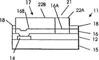
本発明は、図5の側部と対応する図10の頂部に示してあるように、再分配経路設定導体と隆起はんだバンプをもつ微小電子構造11に関する。微小電子構造は、基板15上に接点パッド14と不活性層12を含む。再分配経路設定導体17とはんだバンプ21はそれぞれバンプ下金属層16A−Bとはんだ層22A−Bの各部を含む。
再分配経路設定導体17は、各伸長バンプ下金属部分16Bに比較的長いはんだ部分22Bを含む。はんだバンプ21は、各幅広バンプ下金属部分16Aに幅広はんだ部分22Aを含む。図5に示すように、伸長はんだ部分22Bは比較的薄いが、幅広はんだ部分22Aは隆起しているのが好ましい。
したがって、はんだバンプ21は、接点パッド14から比較的離れた地点に配置され、バンプ21とパッド14は再分配経路設定導体17により電気的に接続されている。この構成は、所定の位置に接点パッド14が配置される基板は第2の位置に関連するはんだバンプを備えている点で有益である。これが特に有益なのは、たとえば、基板がワイヤ接着用に並べられた接点パッドをもつよう設計されているときであり、フリップフロップ分野に基板を使用するのが望ましい。はんだバンプと再分配経路設定導体は、図1ないし10に関して以下に説明されるように、同時に製造可能である。
再分配経路設定導体17は図示のように真っ直ぐであるが、折れたり曲がったりしてもかまわない。さらに、はんだバンプ21は図示のように円形でもよいし、長方形のような他の形状を取ることもできる。
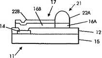
はんだバンプ21と再分配経路設定導体17は同時に形成されるのが好ましい。図1ないし図5は、製造の様々な段階で微小電子構造の横断側面図であり、図6ないし図10は同じ微小電子構造の対応する頂面図である。微小電子構造11は最初に、図1と図6に示すように、基板15上に不活性層12と露出接点パッド14が形成される。
基板15はケイ素、ガリウム、砒化物、炭化ケイ素、ダイアモンド、または当業者に周知の他の基板材料などの半導体材料の層を含むこともできる。半導体材料の層は、トランジスタ、抵抗器、コンデンサおよび/または誘電子などの1つまたは複数の電子デバイスを含むこともできる。接点パッド14は、アルミニウム、銅、チタン、ALCuやAlTi3などの上記の金属を組み合わせた金属間化合物、または当業者に周知の他の材料から形成される。この接点は基板の電子デバイスに接続されるのが好ましい。
不活性層12は、ポリイミド、二酸化ケイ素、窒化ケイ素、または当業者に周知の他の不活性材料を含むことが可能である。図示のように、不活性層12は、基板15に相対する接点パッド14の頂端部を覆い、接点パッド14の中央部分を露出させる。当業者に理解されるように、基板という用語は、図1と図6の不活性層12と接点パッド14を含むものとして定義されている。
図2と図7に示すように、バンプ下金属層16が不活性層上に形成され、はんだバンプと接点パッド14の間を接続して、電気メッキ用の電極が形成される。バンプ下金属層16は、以後の処理工程中に接点パッド14と不活性層12も保護するし、はんだが接着する表面を構成する。バンプ下金属層は不活性層12と接点パッド14上にクロム層を、クロム層上にクロム/銅の段階層を、段階層上に銅層を含むのが好ましい。この構造は、不活性層12と接点パッド14と接着し、それらを保護し、その後にメッキされたはんだの基板ともなる。
バンプ下金属層は、1995年5月20日に出願され本発明の譲受け人に譲渡された米国特許出願「チタン障壁層を含むはんだバンプ製造方法と構造(Solder Bump Fabrication Methods and Structures Including a Titanium Barrier Layer)」に記載された基板とクロム層の間のチタン障壁層を含むこともできる。このチタン障壁層は、バンプ下金属層の他の構成要素を除去するために使用される食刻剤から不活性層を保護して、はんだバンプと再分配経路設定導体間にショートを引き起こしやすい不活性層上に残留物が形成されるのを防ぐ。チタン層は、影響を及ぼすほどの残留物を残すことなく、不活性層から容易に除去できる。
様々なバンプ下金属層が、Dishonによる米国特許第4950623号の「はんだバンプを構築する方法(Method of Building Solder Bumps)」、1995年5月20日に出願されたMisその他による米国特許出願「はんだバンプ製造方法ならびにチタン障壁層を含むはんだバンプ構造(Solder Bump Fabrication Methods and Structures Including a Titanium Barrier Layer)」に開示されている。こうした参照文献はそれぞれ本発明の譲受け人に譲渡され、それぞれの開示はすべて参照のため本明細書に組み込まれている。
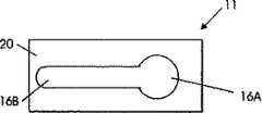
はんだダム18はバンプ下金属層16に形成可能である。このはんだダム18は、バンプ下金属層16の上にチタンやクロムなどのはんだが溶解しない材料の層を含むのが好ましい。はんだにより覆われてないバンプ下金属層の第1(露出)部分を除去する前に再流工程を実行する場合に、はんだダム18ははんだを止めるのに利用される。このことは以下に説明される。マスク層20ははんだダム18上に形成される。マスク層は、フォトレジストマスクまたは当業者に周知の他のマスクを含んでもかまわない。
マスク層20は、バンプ下金属層の第1部分上ではんだダムを覆い、はんだバンプと再分配経路設定導体が形成されるバンプ下金属層16の第2部分上ではんだダムの領域を露出するようにパターン化される。図3と図8に示すように、はんだダムの露出部分が取り除かれて、バンプ下金属層16の第2部分を露出する。具体的には、バンプ下金属層16の第2部分は、はんだダムとパターン化マスク層によって覆われてはおらず、幅広部分16Aと伸長部分16Bを含む。
はんだ層22は、図4と図9に示すように、バンプ下金属層16の第2部分に電気メッキされるのが好ましい。当業者には理解されるように、電気バイアスを連続するバンプ下金属層16に加えて、鉛と錫を含む溶液に微細電子構造を浸すことではんだが電気メッキされる。この電気メッキ処理により、はんだ層がバンプ下金属層16の複数の第2部分に同時に形成できる。はんだはマスク層20にはメッキされない。その代わりに、ペーストとしてスクリーン印刷、蒸着、E光線析出、無電解メッキ、または当業者に周知の他の方法によりはんだが付着される。さらに、本明細書を通して例示のために鉛と錫のはんだが使用されるが、当業者には当然のことながら、鉛とインジウムのはんだまたは錫のはんだが利用できる。
はんだ層22は、伸長部分22Bと幅広部分22Aを含む。マスク層20を除去すると、微小電子構造11が加熱されると、伸長はんだ部分22Bから幅広はんだ部分22Aにはんだが流れて、幅広はんだ部分22Aに隆起はんだバンプが形成される。はんだダム18は、図5と図10に示すように、バンプ下金属層16の伸長部16Bと幅広部16Aを超えてはんだが拡がるのを防いでいる。
はんだが流れ始めるのは、その液相線温度(鉛が90%で錫が10%のはんだでは約299℃)を越えて加熱されたときである。この処理は普通、はんだ再流と呼ばれる。再流中に、はんだの表面張力が、はんだバンプの比較的幅広い形状の幅広はんだ部分22Aに比較的低い内部圧力を、再分配経路設定導体の比較的狭い形状の伸長はんだ部分22Bに比較的高い内部圧力をうみだす。
この異なる内部圧力を同じにするために、はんだが伸長はんだ部分22Bから幅広はんだ部分22Aに流れる。その結果、幅広はんだ部分22Aに隆起はんだバンプが形成され、再分配経路設定導体上の伸長はんだ部分22Bにはんだの比較的薄い層が形成される。はんだがその液相線温度より低く冷却されると、再分配経路設定導体上に隆起はんだバンプとはんだの薄層を含む形状を維持するようにはんだが固形化する。
スクリーン印刷によりプリント回路基板ランドに均一にはんだを塗布するのはプリント回路基板製造技術では周知であるし、はんだの厚みもランドの一部を局所的に増加させることで増加させることができることも周知である。Swansonによる「プリント回路基板組立体:中国の組立て技術(PCB Assembly:Assembly Technology in Chaina)」、電子実装および生産技術(Electronic Packaging & Production)、pp.40,42,1995年1月を参照のこと。しかし、こうした知識としては、はんだが微細電子基板に均一の厚さに電気メッキされ、さらに基板上に再分配経路設定導体を備えた隆起はんだバンプを作りだすようにはんだが加熱されることを実施したのは出願者が初めてである。
さらに、Mooreその他による米国特許第5327013号では、はんだ合金の微小球をパッドに圧接して、高分子はんだ抵抗性材料から形成されたはんだストップをランナーに形成してはんだを接着パッドに閉じ込めることが開示されている。上記特許には接着パッドと比べてランナー断面の幅を縮小させることで再流中のランナーに沿ったはんだの拡大を制限できることは述べてあるが、ランナー断面と接着パッドのそれぞれの寸法を利用してはんだをランナーから接着パッドに流して、様々な厚みのはんだ構造を形成することは示唆されてない。さらに、上述の参照文献のどれにも伸長部分と幅広部分をもつはんだ構造をバンプ下金属層を覆うのに使用して、単一のマスク工程だけで隆起はんだ部をもつ再分配経路設定導体を形成することは教唆されていない。
本発明の方法は、再流(液体)はんだの表面張力誘導内部圧力の差に応じて、伸長はんだ部分22Bではんだの薄層を、伸長幅はんだ部分22Aで隆起はんだバンプを形成する。はんだの液体ドロップの内部圧力Pは以下の式により判定できる。
P=2T/r
ただしTは液体はんだの表面張力、rはドロップの半径である。
バンプ下金属層など平坦な溶解可能面に液体はんだを付着させるる場合には、式は以下のようになる。
P=2T/r'
この式では、r'は液体はんだの見掛けの半径である。見掛けの半径とははんだの露出面により画定された弧(曲率半径)の半径である。見掛けの半径は、はんだと接触するバンプ下金属層の第2部分など基礎はんだ可溶性層の幅により左右される。したがって、再流はんだ構造の内部圧力は、はんだに接触するバンプ下金属の第2部分の幅に反比例している。言い換えれば、比較的広いバンプ下金属部分上のはんだ部分は比較的低い内部圧力をもつことになるが、伸長(相対的に狭い)バンプ下金属部分上のはんだ部分は比較的高い内部圧力をもつことになる。内部圧力が同じになるのは、伸長はんだ部分22Bと幅広はんだ部分22Aの見掛けの半径がほぼ等しくなるときである。
したがって、図4と図9に示された均一の厚みのはんだ層22がその液相線温度を越えて加熱されると、伸長はんだ部分22Bと幅広はんだ部分22Aがそれぞれほぼ同じ見掛けの半径となり、隆起はんだバンプが形成されるまで、はんだは部分22Bから22Aに流れる。はんだ流工程がはんだ構造により覆われてないバンプ下金属層16の第1部分を除去する前に実行される場合には、はんだ部分22A−Bとはんだに隣接したバンプ下金属部分16A−Bの間に金属間化合物が形成可能である。金属間化合物はバンプ下金属組織を除去するのに使用されるどの食刻剤にも耐性がある。したがって、この金属間化合物は、はんだにより覆われてないバンプ下金属組織の第1部分を除去する以下の工程でのはんだの下方切除を抑制する。これは、Yungによる米国特許第5162257号の「はんだバンプ製造方法(Solder Bump Fabrication Method)」で説明されている。この特許は本発明の譲受人に譲渡される。
バンプ下金属層16がはんだ構造に隣接する銅の層を含み、はんだは鉛と錫のはんだであるのが好ましい。したがって、はんだを流す工程により、はんだは銅と反応してはんだ構造に隣接した金属間化合物領域を形成する。この金属間化合物はCu3Snを含むことになる。この金属間化合物は、バンプ下金属層を除去するのに使用されるどの食刻剤とも容易には反応しないので、はんだ構造の切り欠きが減少する。
はんだ層22は、はんだにおおわれてないバンプ下金属組織16とはんだダム18の第1部分を選択的に食刻するためにマスクとして使用される。化学食刻剤は、はんだ部分22A−Bの周囲のバンプ下金属層16を食刻するために使用できる。したがって、追加マスク工程は、バンプ下金属層をパターン化するのに必要となる。言い換えれば、マスク層20の形成とはマスク工程だけであり、この工程だけで、はんだダム18(図3と図8)をパターン化し、メッキ工程(図3と図8)中にバンプ下金属層16の第2部分を選択的に露出し、メッキ工程(図5と図10)の後ではんだにおおわれてないバンプ下金属層の複数の第1部分を除去できる。
その代わりに、はんだ部分22Aと22Bにより覆われてないバンプ下金属層16の複数の第1部分を、はんだを流す前に選択的に除去することができる。この場合には、伸長はんだ部22Bと幅広はんだ部22Aはそれぞれ、バンプ下金属部分の伸長部分16Bと幅広部分16Aに支持されている。液体はんだがバンプ下金属組織に溶解可能な場合も、不活性層12には溶解されない。したがって、不活性層にははんだ流工程中にはんだを含むようになり、はんだダム18を除去できる。
他の実施例では、はんだダムは、バンプ下金属層16上のはんだ非溶解性層と、バンプ下金属層に相対するはんだ非溶解性層上の銅などのはんだ溶解性層を備えることができる。これは、Misその他による1995年3月20日出願の米国特許出願「はんだバンプ製造方法とチタン障壁層を含むはんだバンプ構造(Solder Bump Fabrication Methods and Structures Including a Titanium Barrier Layer)」に開示されており、この出願は本発明の譲受人に譲渡される。はんだ溶解性層によりはんだダムの複数の部分ならびにはんだダムやマスクに覆われてないバンプ下金属層の第2部分にはんだをメッキできる。
したがって、マスク層20ははんだダムの複数の部分ならびにバンプ下金属層16の複数の部分を露出するので、より多くのはんだをメッキできる。はんだ層20とはんだ溶解性層の複数の基礎部分が除去される。はんだが流れるように加熱されると、はんだの下のはんだ溶解性層の残りの部分がはんだに溶け、はんだははんだ非溶解性層に露出される。したがって、はんだは、溶解可能なバンプ下金属層の第2部分に戻ることになる。
例として、バンプ下金属層の第1部分ははんだダム18とマスク層20により覆われている。バンプ下金属層の第2部分は露出しており、この第2部分には、図3と図8に示すように、幅150マイクロミリ長さ500マイクロミリの伸長部16Bと、500マイクロミリの直径(または幅)の円形幅広部16Aがある。次に、図4に示すように、35マイクロミリの均一高をもつはんだ層が、伸長部分16Aと幅広16Bを含むバンプ下金属層16の第2部分に電気メッキされる。このはんだは鉛90%、錫10%である。マスク層を除去した後で、はんだをその液相線温度(約299℃)より高く加熱すれば、はんだは流れ始める。
液体はんだは、はんだが溶解しないはんだダム18によりはんだ溶解性バンプ下金属層の第2部分16A−Bに含まれている。はんだ構造の幅にはバラツキがあるので、はんだ構造の内部圧力は、高さが均一でも同じではない。具体的には、はんだの高さが同じ場合には、伸長はんだ部分22Bの内部圧力は比較的高く(約1.283×10⁴Paまたは1.86psi)、幅広はんだ部分22Aの内部圧力は比較的低い(約3.848×10³Paまたは.558psi)。
したがって、伸長はんだ部分22Bと幅広はんだ部分22Aの内部圧力が等しくなるまではんだが部分22Bから22Aに流れるので、図5と図10に示されるように、幅広はんだ部分22Aに隆起はんだバンプが形成される。図5と図10では、はんだダム18と、はんだ構造により覆われてないバンプ下金属層16の第1部分も除去される。
この例では、約3.4×10³Pa(.493psi)の内部圧力で均衡状態が得られる。均衡状態では、伸長はんだ部分22Bの高さは約10マイクロミリで、幅広はんだ部分の高さは約130マイクロミリであり、両部分とも曲率半径は約281マイクロミリである。したがって、2レベルはんだ構造は単一のマスク工程で形成可能である。冷却すると、この構造は、形状を保持した状態で固まる。さらに、伸長はんだ部分22Bははんだの高さが10マイクロミリあれば、はんだに覆われないバンプ下金属層の第1部分を除去するときに伸長バンプ下金属層部分16Bを覆うのに十分である。上記の方法により形成されたはんだバンプが伸長はんだ部分と比べて十分に隆起しプリント回路基板と適切な接続が確実に確立されるのには、はんだ構造の幅広部分の幅(幅広部分が円形なら半径)は、はんだ構造の伸長部分の幅の少なくとも2倍が必要である。
図面と明細書において、本発明の代表的な好適実施例を開示してきた。特定の用語が使われているが、それらは全体的かつ説明的な意味でのみ使用されており、制限を加えるためではない。本発明の範囲は以下の請求の範囲に詳述される。Field of the invention
The present invention relates to the field of microelectronic devices, and specifically to solder bumps for microelectronic devices.
Background of the Invention
In high performance microelectronic devices, solder balls and solder bumps are often used to electrically and mechanically interconnect with other microelectronic devices. For example, large scale integration (VLSI) chips are electrically connected to circuit boards and other next level mounting substrates using solder balls and solder bumps. This connection technique is also referred to as "controlled flip chip connection-C4" or "flip-flop" technique. In this specification, this is referred to as “solder bump”.
A remarkable advance in this technology is disclosed in U.S. Pat. No. 5,162,257 to Yung, "Method of Manufacturing Solder Bumps." This patent is assigned to the assignee of the present invention. In this patent, an under bump metallurgy is formed on the microelectronic substrate including the contact pads, and a solder bump is formed on the under bump metallurgy opposite the contact pads. The under bump metallurgy between the solder bumps and the contact pads is converted to an intermetallic compound that is resistant to the etchant used to etch the under bump metallurgy between the solder bumps. Therefore, the noble portion of the solder bump is protected.
It is often desirable to form a solder bump on a substrate at a location remote from a contact pad or an electrical contact between the contact pad and the solder bump. For example, microelectronic substrates are initially designed to wire bond to contact pads lined up on the outer edge of the substrate. Second, it is desirable to use it in applications where solder bumps need to be located inside the substrate. Interconnect or redistribution routing conductors are required to place the solder bumps inside the substrate away from each contact pad.
U.S. Pat. No. 5,327,013 to Moore et al., "Solder Bumping of Integrated Circuit Die," discloses a method for forming redistribution routing conductors and solder bumps on an integrated circuit die. In this method, a conductive type solder-soluble composite material terminal is formed. This terminal includes an adhesive pad on the passivation layer remote from the metal contacts. Further, a runner extends from the pad to the metal contact. The solder mass is reflowed to the bond pad to form a bump. The bump is adhered to the pad and is electrically connected via a runner.
However, in this method, the solder bumps are formed by pressing the solder alloy microspheres onto the bonding pads. Furthermore, the spread of solder along the runner during reflow is limited. In an exemplary embodiment, a solder stop made of a polymeric solder resistive material is formed in the runner to confine the solder to the bond pad.
Notwithstanding the above references, there is a continuing need in the art for an efficient and inexpensive method of making redistribution routing conductors and solder bumps.
Summary of the Invention
Accordingly, it is an object of the present invention to provide an improved method of forming a redistribution routing conductor.
It is another object of the present invention to provide a method for forming a redistribution routing conductor that can be formed integrally with an associated solder bump.
In accordance with the present invention, these and other objects are achieved by forming a metal layer under a bump on a microelectronic substrate and forming a solder structure having an extended portion and a wide portion on the metal layer under a bump. The solder structure is formed by electroplating a desired portion of the under bump metal layer defined by the mask. Excess portions of the under bump metallurgy that are not covered by the solder can be selectively removed using the solder structure as a mask. Therefore, once the masking step is performed, the solder structure and the metal layer under the bump can be defined.
Next, the solder is poured. Surprisingly, the surface tension of the solder causes the solder flow to form a thin layer of solder on the extended portions of the metal layer below the bump and raised solder bumps on the wider portions of that layer. Thus, a single solder plating step followed by a solder flow step (usually thermally induced) results in a solder structure having thin extensions and raised ridges.
In one embodiment, the invention includes a method of forming a redistribution routing conductor on a microelectronic substrate having electrical contact pads on a surface of the microelectronic structure. The method comprises the steps of forming a metal layer below the bump on the surface and forming a solder structure on the metal layer below the bump facing the microelectronic substrate. The metal layer under the bumps is in electrical contact with the electrical contact pads, and the solder structure has elongated and widened portions.
Forming the solder structure preferably includes forming a solder structure including an extension extending over the electrical contact pad. The solder structure can define first (exposed) and second (non-exposed) portions of the metal layer under the bump. The step of forming the solder structure is followed by a step of selectively removing a first (exposed) portion of the under bump metal layer that is not covered by the solder structure. Thus, using the solder structure as a mask layer, the first portion of the under-bump metal layer that is not covered by the solder after forming the solder structure is selectively removed, thereby removing the solder structure and the under-bump metal layer. Each photolithography step for patterning becomes unnecessary.
Preferably, the elongated solder portion has a first end corresponding to a contact pad on the metal layer under the bump and a second end connected to the wide portion. Accordingly, the solder structure preferably defines an extended portion and a wide portion of the under bump metal layer, and one end of the extended portion of the under bump metal layer is preferably in electrical contact with the contact pad. It will also be appreciated that other elongated solder portions may also traverse the under bump metal layer in other directions from points facing the contact pads, with the extending portions extending slightly beyond the points facing the contact pads. .
The method also includes flowing the solder of the solder structure from the elongated portion to the wider portion. Thus, raised solder bumps can be formed over a wide portion of the solder structure, and this solder layer can be formed over an extended portion of the solder structure. This process is performed by heating the solder above the liquidus temperature, confining the solder to the extended and wide portions of the metal layer under the bumps, and allowing the solder to flow to the wide portions due to surface tension induced internal pressure. Preferably. Solder flow can be confined by forming a solder dam layer on the first (exposed) portion of the under bump metal layer that is not covered by the solder structure.
The step of allowing the solder to flow forms an intermetallic compound region between the metal layer under the bump and the solder structure. This intermetallic compound region includes, as constituent elements, a metal layer and a solder structure. This intermetallic region is resistant to the etchant used to remove the first (exposed) portion of the metal layer under the bump, thereby reducing downward ablation of the solder structure.
The step of forming the metal layer under the bump is preferably a step of forming a chromium layer on the microelectronic substrate, a step of forming a chromium and copper step layer on the chromium layer, and a step layer opposite to the chromium layer. And a step of forming a copper layer thereon. This structure includes a microelectronic structure, contact pads, and a conductive base that adheres to the solder structure. Forming the metal layer under the bump may include forming a titanium layer between the microelectronic substrate and the chromium layer.
The step of forming the solder structure includes forming a patterned mask layer on the metal layer under the bump, forming a solder structure on the first portion of the metal layer under the bump, and selectively forming the patterned mask layer. And removing. Preferably, the patterned mask layer covers a first portion of the under-bump metal layer and defines a first portion of the under-bump metal layer where the solder structure is to be formed.
Further, forming the solder structure includes electroplating solder on the first portion of the metal layer under the bump. By forming the under-bump metal layer to extend over the microelectronic substrate, the under-bump metal layer can be used as an electroplated electrode for multiple solder structures. Thus, multiple solder structures are formed in a single electroplating process. The height of each solder structure is uniform.
The present invention also includes a solder bump structure on a microelectronic structure that includes electrical contacts with exposed portions. The solder bump structure includes a metal structure under the bump on the microelectronic substrate and a solder structure on the metal structure under the bump facing the microelectronic substrate. The metal structure includes an extension having a first end in electrical contact with an exposed portion of the electrical contact, and a wide portion connected to a second end of the extension. The solder structure includes an elongated portion and a wide portion on the metal structure. Therefore, the wide portion of the solder structure can be formed on a part of the microelectronic substrate other than the contact pads, and is in a state of being electrically connected to the pads.
The elongated portion of the solder structure has a first predetermined thickness, and the wide portion of the solder structure has a second predetermined thickness. The first predetermined thickness is preferably smaller than the second predetermined thickness. Thus, preferably, the wide portions of the solder structure are formed with raised solder bumps that are used to electronically and mechanically connect the microelectronic substrate to a printed circuit board or other next level mounting substrate. Instead, the thickness of the elongated portion and the wide portion of the solder structure are common.
The solder bump structure also includes an intermetallic compound region between the under bump metal structure and the solder structure, the intermetallic compound region including the metal structure and the solder structure as components.
Instead, the solder bump structure includes an under bump metal layer on the microelectronic structure. The under bump metal layer is in electrical contact with the exposed portions of the electrical contacts. This solder bump structure includes a solder structure on the metal layer under the bump, facing the microelectronic substrate. The solder structure includes an elongated portion having a first end opposite the exposed portion of the electrical setting and a widened portion connected to a second end of the elongated portion. The under-bump metal layer extends across the microelectronic substrate and the solder structure defines first (exposed) and second (unexposed) portions of the under-bump metal layer. The metal layer under the continuous bump can be used as an electrode for electroplating.
Further, the structure includes solder dams in the plurality of first (exposed) portions of the under bump metal layer. This solder dam can be used to store the solder during the solder flowing step described above.
Thus, a metal layer under the bump is formed on the microelectronic substrate and can be used as an electrode for electroplating a solder structure including an extended portion and a wide portion. The solder structure is then used to selectively remove portions of the under bump metal layer that are not covered by the solder structure. A single photolithographic step can therefore be used to pattern both the solder structure and the metal layer under the bump. Further, the solder flows from the elongated portions of the solder structure to the wider portions to form raised solder bumps. This is preferably accomplished by heating the solder above the liquidus temperature where surface tension induced internal pressure can affect the flow of the solder. Therefore, a stable multi-level solder structure is created.
[Brief description of the drawings]
1 to 5 are cross-sectional side views of a microelectronic substrate at various stages during the manufacture of a redistribution routing conductor according to the present invention.
6 to 10 are top views of the microelectronic substrate at various stages during the manufacture of the redistribution routing conductors, corresponding to FIGS. 1 to 5, respectively.
Detailed Description of the Preferred Embodiment
The invention is explained in more detail below with reference to the accompanying drawings. However, the present invention may be embodied in various forms and should not be construed as limited to the embodiments set forth herein. Such embodiments are provided so that this disclosure will be thorough and complete, and will fully convey the scope of the invention to those skilled in the art. In the drawings, the thickness of layers and regions are exaggerated for clarity. Like numbers refer to like elements throughout the drawings.
The present invention relates to a
The redistribution
Therefore, the
The redistribution
Preferably, the
As shown in FIGS. 2 and 7, an under
The metal layer under the bump is described in U.S. Patent Application "Solder Bump Fabrication Methods and Structures Including a Titanium," filed May 20, 1995 and assigned to the assignee of the present invention. Barrier Layer) and a titanium barrier layer between the substrate and the chromium layer. This titanium barrier layer protects the inactive layer from the etchant used to remove other components of the metal layer under the bump, and tends to cause a short between the solder bump and the redistribution routing conductor. Prevent residue formation on the active layer. The titanium layer can be easily removed from the inert layer without leaving any significant residue.
Various under bump metal layers are disclosed by Dishon in U.S. Pat. No. 4,950,623, entitled "Method of Building Solder Bumps"; U.S. Pat. And a solder bump structure including a titanium barrier layer (Solder Bump Fabrication Methods and Structures Including a Titanium Barrier Layer). Each such reference is assigned to the assignee of the present invention, the entire disclosures of which are incorporated herein by reference.
The
The
The solder layer 22 is preferably electroplated on the second portion of the under
The solder layer 22 includes an extended portion 22B and a
The solder begins to flow when it is heated above its liquidus temperature (about 299 ° C for 90% lead and 10% tin solder). This process is commonly called solder reflow. During reflow, the surface tension of the solder is such that a relatively low internal pressure is applied to the relatively wide shaped
In order to equalize the different internal pressures, the solder flows from the elongated solder portion 22B to the
It is well known in the printed circuit board manufacturing technology to apply solder uniformly to printed circuit board lands by screen printing, and it is also known that the thickness of solder can be increased by locally increasing a part of the lands. It is. See Swanson's "PCB Assembly: Assembly Technology in Chaina", Electronic Packaging & Production, pp. 40, 42, January 1995. . However, such knowledge has included that the solder is electroplated to a fine electronic substrate to a uniform thickness and the solder is heated to create raised solder bumps with redistribution routing conductors on the substrate. This is the first time for the applicant.
In addition, Moore et al., U.S. Pat.No. 5,327,013, discloses that solder alloy microspheres can be pressed against a pad to form a solder stop formed from a polymeric solder resistive material on a runner to confine the solder to the bond pad. It has been disclosed. Although the above patent states that by reducing the width of the runner cross-section compared to the bonding pad, it is possible to limit the spread of the solder along the runner during reflow, but using the dimensions of the runner cross-section and the bonding pad, respectively. It is not suggested that the solder flow from the runner to the bond pad to form solder structures of varying thickness. In addition, none of the above references use a solder structure with extended and wide portions to cover the metal layer under the bump to provide a redistribution routing conductor with raised solder in only a single mask step. It is not taught to form.
The method of the present invention forms a thin layer of solder at the extended solder portion 22B and a raised solder bump at the extended
P = 2T / r
Here, T is the surface tension of the liquid solder, and r is the radius of the drop.
When applying liquid solder to a flat dissolvable surface, such as a metal layer under a bump, the formula is as follows:
P = 2T / r '
In this equation, r 'is the apparent radius of the liquid solder. The apparent radius is the radius of the arc (radius of curvature) defined by the exposed surface of the solder. The apparent radius depends on the width of the underlying solder-soluble layer, such as the second portion of the metal layer below the bump that contacts the solder. Thus, the internal pressure of the reflow solder structure is inversely proportional to the width of the second portion of the under bump metal that contacts the solder. In other words, a solder portion on a relatively wide under bump metal portion will have a relatively low internal pressure, while a solder portion on an elongated (relatively narrow) under bump metal portion will have a relatively high internal pressure. Will be. The internal pressures are equal when the apparent radii of the elongated solder portion 22B and the
Therefore, when the uniform thickness solder layer 22 shown in FIGS. 4 and 9 is heated above its liquidus temperature, the elongated solder portion 22B and the
The under
The solder layer 22 is used as a mask to selectively etch the
Alternatively, a plurality of first portions of the under
In another embodiment, the solder dam may comprise a solder insoluble layer on the under
Accordingly, more solder can be plated because the
By way of example, a first portion of the metal layer under the bump is covered by a
The liquid solder is contained in the
Therefore, the solder flows from the portions 22B to 22A until the internal pressures of the elongated solder portion 22B and the
In this example, about 3.4 × 10Three Equilibrium is obtained at an internal pressure of Pa (.493 psi). In equilibrium, the height of the elongated solder portion 22B is about 10 micromillimeters, the height of the wide solder portion is about 130 micromillimeters, and both portions have a radius of curvature of about 281 micromillimeters. Thus, a two-level solder structure can be formed in a single mask step. Upon cooling, the structure solidifies while retaining its shape. In addition, the elongated solder portion 22B having a solder height of 10 micrometers is sufficient to cover the elongated under bump
In the drawings and specification, there have been disclosed representative preferred embodiments of the present invention. Certain terms are used, but they are used only in an overall and descriptive sense, and not to limit. The scope of the invention is set forth in the following claims.
Claims (10)
Translated fromJapanese前記微小電子基板上にあり、前記電気接点の露出部分に電気的に接触しているバンプ下金属層と、
前記微小電子基板に相対して前記バンプ下金属層上にあり、伸長部分と幅広部分をもつはんだ構造と、から成ることを特徴とする前記はんだバンプ構造。A solder bump structure for a microelectronic substrate including an electrical contact with an exposed portion,
A metal layer under the bump on the microelectronic substrate and in electrical contact with the exposed portion of the electrical contact;
The solder bump structure, comprising: a solder structure having an elongated portion and a wide portion on the metal layer below the bump, opposite to the microelectronic substrate.
前記表面にバンプ下金属層を形成し、前記電気接点パッドに電気的に接触し、
前記微小電子基板に相対する前記バンプ下金属層上に、伸長部分と幅広部分のあるはんだ構造を形成する工程から構成される再分配経路設定導体を形成する方法。A method of forming a redistribution path setting conductor on a microelectronic substrate including an electric contact pad on a surface of the microelectronic structure,
Forming a metal layer under the bump on the surface, making electrical contact with the electrical contact pad,
A method for forming a redistribution path setting conductor comprising a step of forming a solder structure having an extended portion and a wide portion on the metal layer under a bump facing the microelectronic substrate.
前記バンプ下金属層の前記第1部分にはんだダム層を形成し、
はんだが前記はんだ構造の前記伸長部分から前記はんだ構造の前記幅広部分に流れて、前記バンプ下金属層の前記幅広部分に隆起はんだバンプを、前記バンプ下金属層のの伸長部分にはんだの薄層を形成するように前記はんだ構造がはんだを流す工程を含む請求項4に記載の方法。Wherein the solder structure defines a first portion of the under-bump metal layer not covered by the solder structure and a second portion of the under-bump metal layer covered by the solder structure, the method further comprising: ,
Forming a solder dam layer on the first portion of the metal layer under the bump;
Solder flows from the elongated portion of the solder structure to the widened portion of the solder structure, and raises raised solder bumps to the widened portion of the metal layer below the bump, and a thin layer of solder to the elongated portion of the metal layer below the bump. 5. The method of claim 4, wherein the solder structure includes flowing solder to form a solder.
前記バンプ下金属層にパターン化マスク層を形成し、前記パターン化マスク層は前記バンプ下金属層の前記第1部分を覆い、前記バンプ下金属層の前記第2部分を画定し、
前記バンプ下金属層の前記第2部分に前記はんだ構造を形成し、
前記パターン化マスク層を選択的に除去する工程から構成される請求項4に記載の方法。The solder structure defines a first portion of the under-bump metal layer that is not covered by the solder structure and a second portion of the under-bump metal layer that is covered by the solder structure. The step of forming
Forming a patterned mask layer on the under-bump metal layer, wherein the patterned mask layer covers the first portion of the under-bump metal layer and defines the second portion of the under-bump metal layer;
Forming the solder structure on the second portion of the under bump metal layer;
The method of claim 4, comprising selectively removing the patterned mask layer.
Applications Claiming Priority (3)
| Application Number | Priority Date | Filing Date | Title |
|---|---|---|---|
| US41661995A | 1995-04-05 | 1995-04-05 | |
| US08/416,619 | 1995-04-05 | ||
| PCT/US1996/003751WO1996031905A1 (en) | 1995-04-05 | 1996-03-21 | A solder bump structure for a microelectronic substrate |
Publications (2)
| Publication Number | Publication Date |
|---|---|
| JPH11503566A JPH11503566A (en) | 1999-03-26 |
| JP3549208B2true JP3549208B2 (en) | 2004-08-04 |
Family
ID=23650663
Family Applications (1)
| Application Number | Title | Priority Date | Filing Date |
|---|---|---|---|
| JP53031796AExpired - LifetimeJP3549208B2 (en) | 1995-04-05 | 1996-03-21 | Integrated redistribution routing conductors, solder vipes and methods of forming structures formed thereby |
Country Status (9)
| Country | Link |
|---|---|
| US (3) | US5892179A (en) |
| EP (1) | EP0819318B1 (en) |
| JP (1) | JP3549208B2 (en) |
| KR (2) | KR100425750B1 (en) |
| CN (1) | CN1179412C (en) |
| AT (1) | ATE240586T1 (en) |
| AU (1) | AU5316996A (en) |
| DE (1) | DE69628161T2 (en) |
| WO (1) | WO1996031905A1 (en) |
Families Citing this family (95)
| Publication number | Priority date | Publication date | Assignee | Title |
|---|---|---|---|---|
| US6388203B1 (en) | 1995-04-04 | 2002-05-14 | Unitive International Limited | Controlled-shaped solder reservoirs for increasing the volume of solder bumps, and structures formed thereby |
| ATE240586T1 (en) | 1995-04-05 | 2003-05-15 | Unitive Int Ltd | A SOLDER BUMP STRUCTURE FOR A MICROELECTRONIC SUBSTRATE |
| US5851911A (en) | 1996-03-07 | 1998-12-22 | Micron Technology, Inc. | Mask repattern process |
| US5902686A (en)* | 1996-11-21 | 1999-05-11 | Mcnc | Methods for forming an intermetallic region between a solder bump and an under bump metallurgy layer and related structures |
| GB2341705B (en)* | 1997-06-26 | 2003-01-29 | Charles Schwab & Co Inc | System and method for automatically providing financial services to a user using speech signals |
| EP0899787A3 (en)* | 1997-07-25 | 2001-05-16 | Mcnc | Controlled-shaped solder reservoirs for increasing the volume of solder bumps, and structurs formed thereby |
| US6441487B2 (en)* | 1997-10-20 | 2002-08-27 | Flip Chip Technologies, L.L.C. | Chip scale package using large ductile solder balls |
| EP1082884B1 (en)* | 1998-06-02 | 2002-01-16 | Siemens S.A. | Method for producing wirings having solder bumps |
| US6085968A (en)* | 1999-01-22 | 2000-07-11 | Hewlett-Packard Company | Solder retention ring for improved solder bump formation |
| US6380555B1 (en)* | 1999-12-24 | 2002-04-30 | Micron Technology, Inc. | Bumped semiconductor component having test pads, and method and system for testing bumped semiconductor components |
| US6373137B1 (en)* | 2000-03-21 | 2002-04-16 | Micron Technology, Inc. | Copper interconnect for an integrated circuit and methods for its fabrication |
| US6362087B1 (en)* | 2000-05-05 | 2002-03-26 | Aptos Corporation | Method for fabricating a microelectronic fabrication having formed therein a redistribution structure |
| KR100668809B1 (en)* | 2000-06-30 | 2007-01-16 | 주식회사 하이닉스반도체 | Wafer level package |
| TW494548B (en)* | 2000-08-25 | 2002-07-11 | I-Ming Chen | Semiconductor chip device and its package method |
| US6666368B2 (en) | 2000-11-10 | 2003-12-23 | Unitive Electronics, Inc. | Methods and systems for positioning substrates using spring force of phase-changeable bumps therebetween |
| DE60108413T2 (en) | 2000-11-10 | 2005-06-02 | Unitive Electronics, Inc. | METHOD FOR POSITIONING COMPONENTS WITH THE HELP OF LIQUID DRIVES AND STRUCTURES THEREFOR |
| US6418033B1 (en) | 2000-11-16 | 2002-07-09 | Unitive Electronics, Inc. | Microelectronic packages in which second microelectronic substrates are oriented relative to first microelectronic substrates at acute angles |
| TW517334B (en)* | 2000-12-08 | 2003-01-11 | Nec Corp | Method of forming barrier layers for solder bumps |
| US6863209B2 (en) | 2000-12-15 | 2005-03-08 | Unitivie International Limited | Low temperature methods of bonding components |
| JP4656275B2 (en)* | 2001-01-15 | 2011-03-23 | 日本電気株式会社 | Manufacturing method of semiconductor device |
| JP2002222578A (en)* | 2001-01-26 | 2002-08-09 | Nitto Denko Corp | Relay flexible wiring circuit board |
| US6956999B2 (en) | 2001-02-20 | 2005-10-18 | Cyberoptics Corporation | Optical device |
| US20040212802A1 (en)* | 2001-02-20 | 2004-10-28 | Case Steven K. | Optical device with alignment compensation |
| US6546172B2 (en) | 2001-02-20 | 2003-04-08 | Avanti Optics Corporation | Optical device |
| US6546173B2 (en)* | 2001-02-20 | 2003-04-08 | Avanti Optics Corporation | Optical module |
| US6443631B1 (en) | 2001-02-20 | 2002-09-03 | Avanti Optics Corporation | Optical module with solder bond |
| US6759319B2 (en) | 2001-05-17 | 2004-07-06 | Institute Of Microelectronics | Residue-free solder bumping process |
| US6502231B1 (en) | 2001-05-31 | 2002-12-31 | Applied Micro Circuits Corporation | Integrated circuit template cell system and method |
| US6550665B1 (en)* | 2001-06-06 | 2003-04-22 | Indigo Systems Corporation | Method for electrically interconnecting large contact arrays using eutectic alloy bumping |
| US6541303B2 (en)* | 2001-06-20 | 2003-04-01 | Micron Technology, Inc. | Method for conducting heat in a flip-chip assembly |
| US6762122B2 (en)* | 2001-09-27 | 2004-07-13 | Unitivie International Limited | Methods of forming metallurgy structures for wire and solder bonding |
| EP1310436A1 (en)* | 2001-11-09 | 2003-05-14 | SOLVAY POLYOLEFINS EUROPE - BELGIUM (Société Anonyme) | Screw cap comprising a multimodal polyethylene composition |
| US7310039B1 (en) | 2001-11-30 | 2007-12-18 | Silicon Laboratories Inc. | Surface inductor |
| US6644536B2 (en)* | 2001-12-28 | 2003-11-11 | Intel Corporation | Solder reflow with microwave energy |
| US7531898B2 (en) | 2002-06-25 | 2009-05-12 | Unitive International Limited | Non-Circular via holes for bumping pads and related structures |
| US7547623B2 (en) | 2002-06-25 | 2009-06-16 | Unitive International Limited | Methods of forming lead free solder bumps |
| WO2004001837A2 (en) | 2002-06-25 | 2003-12-31 | Unitive International Limited | Methods of forming electronic structures including conductive shunt layers and related structures |
| US7632750B2 (en)* | 2006-07-07 | 2009-12-15 | Semigear Inc | Arrangement for solder bump formation on wafers |
| US6965160B2 (en)* | 2002-08-15 | 2005-11-15 | Micron Technology, Inc. | Semiconductor dice packages employing at least one redistribution layer |
| GB2408111A (en)* | 2002-08-20 | 2005-05-18 | Cyberoptics Corp | Optical alignment mount with height adjustment |
| US6964881B2 (en)* | 2002-08-27 | 2005-11-15 | Micron Technology, Inc. | Multi-chip wafer level system packages and methods of forming same |
| US7141883B2 (en)* | 2002-10-15 | 2006-11-28 | Silicon Laboratories Inc. | Integrated circuit package configuration incorporating shielded circuit element structure |
| US20040222511A1 (en)* | 2002-10-15 | 2004-11-11 | Silicon Laboratories, Inc. | Method and apparatus for electromagnetic shielding of a circuit element |
| US7135780B2 (en) | 2003-02-12 | 2006-11-14 | Micron Technology, Inc. | Semiconductor substrate for build-up packages |
| TWI225899B (en) | 2003-02-18 | 2005-01-01 | Unitive Semiconductor Taiwan C | Etching solution and method for manufacturing conductive bump using the etching solution to selectively remove barrier layer |
| TWI255538B (en)* | 2003-06-09 | 2006-05-21 | Siliconware Precision Industries Co Ltd | Semiconductor package having conductive bumps on chip and method for fabricating the same |
| US6960820B2 (en)* | 2003-07-01 | 2005-11-01 | International Business Machines Corporation | Bipolar transistor self-alignment with raised extrinsic base extension and methods of forming same |
| KR100546346B1 (en)* | 2003-07-23 | 2006-01-26 | 삼성전자주식회사 | Rewiring bump formation method and semiconductor chip and mounting structure using same |
| US7244671B2 (en)* | 2003-07-25 | 2007-07-17 | Unitive International Limited | Methods of forming conductive structures including titanium-tungsten base layers and related structures |
| US7416106B1 (en)* | 2003-09-29 | 2008-08-26 | Emc Corporation | Techniques for creating optimized pad geometries for soldering |
| US7049216B2 (en) | 2003-10-14 | 2006-05-23 | Unitive International Limited | Methods of providing solder structures for out plane connections |
| KR100994768B1 (en)* | 2003-12-08 | 2010-11-16 | 삼성전자주식회사 | Motion Estimation Method for Motion Picture Coding and Recording Media with Program for Implementing It |
| US7427557B2 (en)* | 2004-03-10 | 2008-09-23 | Unitive International Limited | Methods of forming bumps using barrier layers as etch masks |
| TW200603698A (en) | 2004-04-13 | 2006-01-16 | Unitive International Ltd | Methods of forming solder bumps on exposed metal pads and related structures |
| DE102004035080A1 (en)* | 2004-05-27 | 2005-12-29 | Infineon Technologies Ag | Arrangement for reducing electrical crosstalk on a chip |
| US9318428B2 (en)* | 2004-05-28 | 2016-04-19 | Nxp B.V. | Chip having two groups of chip contacts |
| US7375411B2 (en)* | 2004-06-03 | 2008-05-20 | Silicon Laboratories Inc. | Method and structure for forming relatively dense conductive layers |
| US6977213B1 (en) | 2004-08-27 | 2005-12-20 | Taiwan Semiconductor Manufacturing Company, Ltd. | IC chip solder bump structure and method of manufacturing same |
| US7419852B2 (en)* | 2004-08-27 | 2008-09-02 | Micron Technology, Inc. | Low temperature methods of forming back side redistribution layers in association with through wafer interconnects, semiconductor devices including same, and assemblies |
| DE102004046699A1 (en)* | 2004-09-24 | 2006-04-13 | Infineon Technologies Ag | Contact surfaces e.g. cooling unit, connecting device, has contact surfaces connected by solidifying liquid e.g. melted solder, such that section of one of two surface edges exhibits structuring in area of edges |
| US20060205170A1 (en)* | 2005-03-09 | 2006-09-14 | Rinne Glenn A | Methods of forming self-healing metal-insulator-metal (MIM) structures and related devices |
| US7501924B2 (en)* | 2005-09-30 | 2009-03-10 | Silicon Laboratories Inc. | Self-shielding inductor |
| US20070090156A1 (en)* | 2005-10-25 | 2007-04-26 | Ramanathan Lakshmi N | Method for forming solder contacts on mounted substrates |
| US7932615B2 (en)* | 2006-02-08 | 2011-04-26 | Amkor Technology, Inc. | Electronic devices including solder bumps on compliant dielectric layers |
| US7674701B2 (en) | 2006-02-08 | 2010-03-09 | Amkor Technology, Inc. | Methods of forming metal layers using multi-layer lift-off patterns |
| US7723224B2 (en)* | 2006-06-14 | 2010-05-25 | Freescale Semiconductor, Inc. | Microelectronic assembly with back side metallization and method for forming the same |
| TWI313037B (en)* | 2006-12-12 | 2009-08-01 | Siliconware Precision Industries Co Ltd | Chip scale package structure and method for fabricating the same |
| US8084695B2 (en)* | 2007-01-10 | 2011-12-27 | Hsu Hsiuan-Ju | Via structure for improving signal integrity |
| CN101226889B (en)* | 2007-01-15 | 2010-05-19 | 百慕达南茂科技股份有限公司 | Reconfiguration line structure and manufacturing method thereof |
| US7834449B2 (en)* | 2007-04-30 | 2010-11-16 | Broadcom Corporation | Highly reliable low cost structure for wafer-level ball grid array packaging |
| KR101350972B1 (en)* | 2007-05-18 | 2014-01-14 | 엘지디스플레이 주식회사 | Backlight unit and liquid crystal display device module including the same |
| US7858438B2 (en)* | 2007-06-13 | 2010-12-28 | Himax Technologies Limited | Semiconductor device, chip package and method of fabricating the same |
| CN101360388B (en)* | 2007-08-01 | 2010-10-13 | 全懋精密科技股份有限公司 | Electrical connection end structure of circuit board and manufacturing method thereof |
| US7872347B2 (en) | 2007-08-09 | 2011-01-18 | Broadcom Corporation | Larger than die size wafer-level redistribution packaging process |
| FR2920634A1 (en)* | 2007-08-29 | 2009-03-06 | St Microelectronics Grenoble | METHOD FOR MANUFACTURING PLATES FOR THE ELECTRICAL CONNECTION OF A PLATE. |
| FR2924302B1 (en)* | 2007-11-23 | 2010-10-22 | St Microelectronics Grenoble | METHOD FOR MANUFACTURING PLATES FOR THE ELECTRICAL CONNECTION OF A PLATE |
| CN101459088B (en)* | 2007-12-13 | 2010-06-09 | 中芯国际集成电路制造(上海)有限公司 | Redistribution metal layer and manufacturing method for redistribution convex point |
| CN101355066B (en)* | 2008-05-26 | 2011-05-18 | 苏州晶方半导体科技股份有限公司 | Packaging structure and manufacturing method thereof |
| US8643164B2 (en) | 2009-06-11 | 2014-02-04 | Broadcom Corporation | Package-on-package technology for fan-out wafer-level packaging |
| US8362612B1 (en)* | 2010-03-19 | 2013-01-29 | Amkor Technology, Inc. | Semiconductor device and manufacturing method thereof |
| US8441124B2 (en)* | 2010-04-29 | 2013-05-14 | Taiwan Semiconductor Manufacturing Company, Ltd. | Cu pillar bump with non-metal sidewall protection structure |
| TWI555100B (en) | 2010-07-26 | 2016-10-21 | 矽品精密工業股份有限公司 | Chip scale package and fabrication method thereof |
| TWI423355B (en) | 2010-08-04 | 2014-01-11 | 矽品精密工業股份有限公司 | Chip-sized package and fabrication method thereof |
| TWI426587B (en) | 2010-08-12 | 2014-02-11 | 矽品精密工業股份有限公司 | Chip scale package and fabrication method thereof |
| JP5537341B2 (en)* | 2010-08-31 | 2014-07-02 | 株式会社東芝 | Semiconductor device |
| US8288203B2 (en)* | 2011-02-25 | 2012-10-16 | Stats Chippac, Ltd. | Semiconductor device and method of forming a wafer level package structure using conductive via and exposed bump |
| US8648664B2 (en) | 2011-09-30 | 2014-02-11 | Silicon Laboratories Inc. | Mutual inductance circuits |
| KR20140041975A (en) | 2012-09-25 | 2014-04-07 | 삼성전자주식회사 | Bump structures and electrical connection structures having the bump structures |
| US8802556B2 (en)* | 2012-11-14 | 2014-08-12 | Qualcomm Incorporated | Barrier layer on bump and non-wettable coating on trace |
| US9236320B2 (en)* | 2013-06-28 | 2016-01-12 | Xintec Inc. | Chip package |
| US9466590B1 (en)* | 2015-11-13 | 2016-10-11 | International Business Machines Corporation | Optimized solder pads for microelectronic components |
| KR102315634B1 (en)* | 2016-01-13 | 2021-10-22 | 삼원액트 주식회사 | A Circuit Board |
| US10120971B2 (en)* | 2016-08-30 | 2018-11-06 | Taiwan Semiconductor Manufacturing Co., Ltd. | Integrated fan-out package and layout method thereof |
| US11158595B2 (en)* | 2017-07-07 | 2021-10-26 | Texas Instruments Incorporated | Embedded die package multichip module |
| US12021048B2 (en)* | 2021-08-30 | 2024-06-25 | Taiwan Semiconductor Manufacturing Company, Ltd. | Semiconductor device |
Family Cites Families (76)
| Publication number | Priority date | Publication date | Assignee | Title |
|---|---|---|---|---|
| US3259814A (en) | 1955-05-20 | 1966-07-05 | Rca Corp | Power semiconductor assembly including heat dispersing means |
| DE1182353C2 (en) | 1961-03-29 | 1973-01-11 | Siemens Ag | Method for manufacturing a semiconductor component, such as a semiconductor current gate or a surface transistor, with a high-resistance n-zone between two p-zones in the semiconductor body |
| US3244947A (en) | 1962-06-15 | 1966-04-05 | Slater Electric Inc | Semi-conductor diode and manufacture thereof |
| US3274458A (en) | 1964-04-02 | 1966-09-20 | Int Rectifier Corp | Extremely high voltage silicon device |
| US3458925A (en) | 1966-01-20 | 1969-08-05 | Ibm | Method of forming solder mounds on substrates |
| DE1614928A1 (en)* | 1966-07-19 | 1970-12-23 | Solitron Devices | Method for contacting semiconductor components |
| DE1764096A1 (en) | 1967-04-04 | 1971-05-27 | Marconi Co Ltd | Surface field effect transistor |
| US3461357A (en) | 1967-09-15 | 1969-08-12 | Ibm | Multilevel terminal metallurgy for semiconductor devices |
| NL159822B (en)* | 1969-01-02 | 1979-03-15 | Philips Nv | SEMICONDUCTOR DEVICE. |
| GB1288564A (en)* | 1969-01-24 | 1972-09-13 | ||
| US3871014A (en)* | 1969-08-14 | 1975-03-11 | Ibm | Flip chip module with non-uniform solder wettable areas on the substrate |
| US3871015A (en)* | 1969-08-14 | 1975-03-11 | Ibm | Flip chip module with non-uniform connector joints |
| US3663184A (en)* | 1970-01-23 | 1972-05-16 | Fairchild Camera Instr Co | Solder bump metallization system using a titanium-nickel barrier layer |
| DE2044494B2 (en)* | 1970-09-08 | 1972-01-13 | Siemens AG, 1000 Berlin u 8000 München | CONNECTING AREAS FOR SOLDERING SEMI-CONDUCTOR COMPONENTS IN FLIP CHIP TECHNOLOGY |
| US3760238A (en)* | 1972-02-28 | 1973-09-18 | Microsystems Int Ltd | Fabrication of beam leads |
| JPS49135749U (en) | 1973-03-24 | 1974-11-21 | ||
| US4113578A (en)* | 1973-05-31 | 1978-09-12 | Honeywell Inc. | Microcircuit device metallization |
| US3959577A (en) | 1974-06-10 | 1976-05-25 | Westinghouse Electric Corporation | Hermetic seals for insulating-casing structures |
| US3993123A (en) | 1975-10-28 | 1976-11-23 | International Business Machines Corporation | Gas encapsulated cooling module |
| US4257905A (en) | 1977-09-06 | 1981-03-24 | The United States Of America As Represented By The United States Department Of Energy | Gaseous insulators for high voltage electrical equipment |
| JPS5459080A (en)* | 1977-10-19 | 1979-05-12 | Nec Corp | Semiconductor device |
| US4168480A (en) | 1978-02-13 | 1979-09-18 | Torr Laboratories, Inc. | Relay assembly |
| JPS55111127A (en)* | 1979-02-19 | 1980-08-27 | Fuji Electric Co Ltd | Method for forming solder bump |
| JPS5678356U (en) | 1979-11-12 | 1981-06-25 | ||
| US4273859A (en) | 1979-12-31 | 1981-06-16 | Honeywell Information Systems Inc. | Method of forming solder bump terminals on semiconductor elements |
| JPS5773952A (en)* | 1980-10-27 | 1982-05-08 | Hitachi Ltd | Chip for face down bonding and production thereof |
| JPS57197838A (en)* | 1981-05-29 | 1982-12-04 | Oki Electric Ind Co Ltd | Semiconductor flip chip element |
| US4449580A (en) | 1981-06-30 | 1984-05-22 | International Business Machines Corporation | Vertical wall elevated pressure heat dissipation system |
| JPS58146827A (en) | 1982-02-25 | 1983-09-01 | Fuji Electric Co Ltd | Semiconductor pressure sensor |
| CH664040A5 (en) | 1982-07-19 | 1988-01-29 | Bbc Brown Boveri & Cie | PRESSURE GAS-INSULATED CURRENT TRANSFORMER. |
| JPS59154041A (en)* | 1983-02-22 | 1984-09-03 | Fuji Electric Corp Res & Dev Ltd | Formation of electrode of semiconductor device |
| JPS602011A (en) | 1983-06-14 | 1985-01-08 | 三菱電機株式会社 | gas insulated electrical equipment |
| US4545610A (en)* | 1983-11-25 | 1985-10-08 | International Business Machines Corporation | Method for forming elongated solder connections between a semiconductor device and a supporting substrate |
| US4661375A (en) | 1985-04-22 | 1987-04-28 | At&T Technologies, Inc. | Method for increasing the height of solder bumps |
| JPS6116552A (en)* | 1985-06-21 | 1986-01-24 | Hitachi Ltd | Integrated circuit device |
| US4878611A (en)* | 1986-05-30 | 1989-11-07 | American Telephone And Telegraph Company, At&T Bell Laboratories | Process for controlling solder joint geometry when surface mounting a leadless integrated circuit package on a substrate |
| GB2194387A (en) | 1986-08-20 | 1988-03-02 | Plessey Co Plc | Bonding integrated circuit devices |
| JPH0793304B2 (en)* | 1987-03-11 | 1995-10-09 | 富士通株式会社 | Method of forming bump electrode |
| JPS6461934A (en)* | 1987-09-02 | 1989-03-08 | Nippon Denso Co | Semiconductor device and manufacture thereof |
| US4897508A (en) | 1988-02-10 | 1990-01-30 | Olin Corporation | Metal electronic package |
| JPH01214141A (en) | 1988-02-23 | 1989-08-28 | Nec Corp | Flip-chip type semiconductor device |
| US4840302A (en) | 1988-04-15 | 1989-06-20 | International Business Machines Corporation | Chromium-titanium alloy |
| US4927505A (en) | 1988-07-05 | 1990-05-22 | Motorola Inc. | Metallization scheme providing adhesion and barrier properties |
| US4950623A (en)* | 1988-08-02 | 1990-08-21 | Microelectronics Center Of North Carolina | Method of building solder bumps |
| CA2002213C (en) | 1988-11-10 | 1999-03-30 | Iwona Turlik | High performance integrated circuit chip package and method of making same |
| US5024372A (en) | 1989-01-03 | 1991-06-18 | Motorola, Inc. | Method of making high density solder bumps and a substrate socket for high density solder bumps |
| US4962058A (en)* | 1989-04-14 | 1990-10-09 | International Business Machines Corporation | Process for fabricating multi-level integrated circuit wiring structure from a single metal deposit |
| US5048747A (en) | 1989-06-27 | 1991-09-17 | At&T Bell Laboratories | Solder assembly of components |
| US5135155A (en) | 1989-08-25 | 1992-08-04 | International Business Machines Corporation | Thermocompression bonding in integrated circuit packaging |
| FR2663784B1 (en)* | 1990-06-26 | 1997-01-31 | Commissariat Energie Atomique | PROCESS FOR PRODUCING A STAGE OF AN INTEGRATED CIRCUIT. |
| JPH04150033A (en)* | 1990-10-12 | 1992-05-22 | Sharp Corp | Bumps on electronic circuit board and method for forming bumps and circuit patterns on electronic circuit board |
| US5250843A (en)* | 1991-03-27 | 1993-10-05 | Integrated System Assemblies Corp. | Multichip integrated circuit modules |
| US5194137A (en)* | 1991-08-05 | 1993-03-16 | Motorola Inc. | Solder plate reflow method for forming solder-bumped terminals |
| US5160409A (en)* | 1991-08-05 | 1992-11-03 | Motorola, Inc. | Solder plate reflow method for forming a solder bump on a circuit trace intersection |
| WO1993002831A1 (en) | 1991-08-05 | 1993-02-18 | Motorola, Inc. | Solder plate reflow method for forming a solder bump on a circuit trace |
| US5162257A (en)* | 1991-09-13 | 1992-11-10 | Mcnc | Solder bump fabrication method |
| US5923539A (en) | 1992-01-16 | 1999-07-13 | Hitachi, Ltd. | Multilayer circuit substrate with circuit repairing function, and electronic circuit device |
| US5371431A (en) | 1992-03-04 | 1994-12-06 | Mcnc | Vertical microelectronic field emission devices including elongate vertical pillars having resistive bottom portions |
| US5281684A (en)* | 1992-04-30 | 1994-01-25 | Motorola, Inc. | Solder bumping of integrated circuit die |
| JPH0637143A (en) | 1992-07-15 | 1994-02-10 | Toshiba Corp | Semiconductor device and method of manufacturing semiconductor device |
| US5448014A (en) | 1993-01-27 | 1995-09-05 | Trw Inc. | Mass simultaneous sealing and electrical connection of electronic devices |
| US5479042A (en) | 1993-02-01 | 1995-12-26 | Brooktree Corporation | Micromachined relay and method of forming the relay |
| KR940023325A (en)* | 1993-03-11 | 1994-10-22 | 토모마쯔 켕고 | Circuit boards used by precoating the solder layer and circuit boards precoated with the solder layer |
| FR2705832B1 (en) | 1993-05-28 | 1995-06-30 | Commissariat Energie Atomique | Method for producing a sealing bead and mechanical strength between a substrate and a chip hybridized by balls on the substrate. |
| JP3263875B2 (en) | 1993-08-24 | 2002-03-11 | ソニー株式会社 | Method for manufacturing surface-mounted electronic component and surface-mounted electronic component |
| US5802699A (en) | 1994-06-07 | 1998-09-08 | Tessera, Inc. | Methods of assembling microelectronic assembly with socket for engaging bump leads |
| US5492235A (en)* | 1995-12-18 | 1996-02-20 | Intel Corporation | Process for single mask C4 solder bump fabrication |
| US5557502A (en) | 1995-03-02 | 1996-09-17 | Intel Corporation | Structure of a thermally and electrically enhanced plastic ball grid array package |
| US5547740A (en)* | 1995-03-23 | 1996-08-20 | Delco Electronics Corporation | Solderable contacts for flip chip integrated circuit devices |
| US5760526A (en) | 1995-04-03 | 1998-06-02 | Motorola, Inc. | Plastic encapsulated SAW device |
| ATE240586T1 (en) | 1995-04-05 | 2003-05-15 | Unitive Int Ltd | A SOLDER BUMP STRUCTURE FOR A MICROELECTRONIC SUBSTRATE |
| US5773359A (en) | 1995-12-26 | 1998-06-30 | Motorola, Inc. | Interconnect system and method of fabrication |
| US5851911A (en)* | 1996-03-07 | 1998-12-22 | Micron Technology, Inc. | Mask repattern process |
| US5736456A (en)* | 1996-03-07 | 1998-04-07 | Micron Technology, Inc. | Method of forming conductive bumps on die for flip chip applications |
| US6025767A (en) | 1996-08-05 | 2000-02-15 | Mcnc | Encapsulated micro-relay modules and methods of fabricating same |
| US5898574A (en) | 1997-09-02 | 1999-04-27 | Tan; Wiling | Self aligning electrical component |
- 1996
- 1996-03-21ATAT96909782Tpatent/ATE240586T1/ennot_activeIP Right Cessation
- 1996-03-21KRKR1019970706975Apatent/KR100425750B1/ennot_activeExpired - Fee Related
- 1996-03-21CNCNB96193624XApatent/CN1179412C/ennot_activeExpired - Fee Related
- 1996-03-21DEDE69628161Tpatent/DE69628161T2/ennot_activeExpired - Fee Related
- 1996-03-21EPEP96909782Apatent/EP0819318B1/ennot_activeExpired - Lifetime
- 1996-03-21WOPCT/US1996/003751patent/WO1996031905A1/enactiveIP Right Grant
- 1996-03-21AUAU53169/96Apatent/AU5316996A/ennot_activeAbandoned
- 1996-03-21JPJP53031796Apatent/JP3549208B2/ennot_activeExpired - Lifetime
- 1997
- 1997-10-02KRKR19977006975Apatent/KR19987003571A/enactivePending
- 1997-11-24USUS08/977,258patent/US5892179A/ennot_activeExpired - Lifetime
- 1999
- 1999-04-05USUS09/286,143patent/US6329608B1/ennot_activeExpired - Lifetime
- 1999-04-05USUS09/286,015patent/US6389691B1/ennot_activeExpired - Lifetime
Also Published As
| Publication number | Publication date |
|---|---|
| AU5316996A (en) | 1996-10-23 |
| EP0819318B1 (en) | 2003-05-14 |
| EP0819318A1 (en) | 1998-01-21 |
| US6389691B1 (en) | 2002-05-21 |
| DE69628161T2 (en) | 2004-03-25 |
| US5892179A (en) | 1999-04-06 |
| HK1008266A1 (en) | 1999-05-07 |
| JPH11503566A (en) | 1999-03-26 |
| ATE240586T1 (en) | 2003-05-15 |
| KR19980703571A (en) | 1998-11-05 |
| DE69628161D1 (en) | 2003-06-18 |
| US6329608B1 (en) | 2001-12-11 |
| KR19987003571A (en) | 1998-11-05 |
| CN1183169A (en) | 1998-05-27 |
| KR100425750B1 (en) | 2004-07-16 |
| CN1179412C (en) | 2004-12-08 |
| WO1996031905A1 (en) | 1996-10-10 |
Similar Documents
| Publication | Publication Date | Title |
|---|---|---|
| JP3549208B2 (en) | Integrated redistribution routing conductors, solder vipes and methods of forming structures formed thereby | |
| US5902686A (en) | Methods for forming an intermetallic region between a solder bump and an under bump metallurgy layer and related structures | |
| US5698465A (en) | Process for manufacturing an interconnect bump for flip-chip integrated circuit including integral standoff and hourglass shaped solder coating | |
| US6570251B1 (en) | Under bump metalization pad and solder bump connections | |
| US6740577B2 (en) | Method of forming a small pitch torch bump for mounting high-performance flip-flop devices | |
| US5767010A (en) | Solder bump fabrication methods and structure including a titanium barrier layer | |
| US6147413A (en) | Mask repattern process | |
| US6415974B2 (en) | Structure of solder bumps with improved coplanarity and method of forming solder bumps with improved coplanarity | |
| US6232212B1 (en) | Flip chip bump bonding | |
| US7906425B2 (en) | Fluxless bumping process | |
| US6429046B1 (en) | Flip chip device and method of manufacture | |
| JP3425526B2 (en) | Controlled shape solder reservoir for increasing the volume of solder protrusion and structure formed thereby | |
| US6897141B2 (en) | Solder terminal and fabricating method thereof | |
| JP2003297866A (en) | Method for manufacturing flip-chip type IC | |
| JP3967999B2 (en) | Flip chip type IC manufacturing method | |
| HK1008266B (en) | A solder bump structure for a microelectronic substrate | |
| JPH01238132A (en) | Electrode for solder join and manufacture of the same |
Legal Events
| Date | Code | Title | Description |
|---|---|---|---|
| TRDD | Decision of grant or rejection written | ||
| A01 | Written decision to grant a patent or to grant a registration (utility model) | Free format text:JAPANESE INTERMEDIATE CODE: A01 Effective date:20040330 | |
| A61 | First payment of annual fees (during grant procedure) | Free format text:JAPANESE INTERMEDIATE CODE: A61 Effective date:20040420 | |
| R150 | Certificate of patent or registration of utility model | Free format text:JAPANESE INTERMEDIATE CODE: R150 | |
| R250 | Receipt of annual fees | Free format text:JAPANESE INTERMEDIATE CODE: R250 | |
| FPAY | Renewal fee payment (event date is renewal date of database) | Free format text:PAYMENT UNTIL: 20090430 Year of fee payment:5 | |
| FPAY | Renewal fee payment (event date is renewal date of database) | Free format text:PAYMENT UNTIL: 20090430 Year of fee payment:5 | |
| FPAY | Renewal fee payment (event date is renewal date of database) | Free format text:PAYMENT UNTIL: 20100430 Year of fee payment:6 | |
| FPAY | Renewal fee payment (event date is renewal date of database) | Free format text:PAYMENT UNTIL: 20100430 Year of fee payment:6 | |
| FPAY | Renewal fee payment (event date is renewal date of database) | Free format text:PAYMENT UNTIL: 20110430 Year of fee payment:7 | |
| FPAY | Renewal fee payment (event date is renewal date of database) | Free format text:PAYMENT UNTIL: 20120430 Year of fee payment:8 | |
| FPAY | Renewal fee payment (event date is renewal date of database) | Free format text:PAYMENT UNTIL: 20120430 Year of fee payment:8 | |
| FPAY | Renewal fee payment (event date is renewal date of database) | Free format text:PAYMENT UNTIL: 20130430 Year of fee payment:9 | |
| FPAY | Renewal fee payment (event date is renewal date of database) | Free format text:PAYMENT UNTIL: 20130430 Year of fee payment:9 | |
| FPAY | Renewal fee payment (event date is renewal date of database) | Free format text:PAYMENT UNTIL: 20140430 Year of fee payment:10 | |
| R250 | Receipt of annual fees | Free format text:JAPANESE INTERMEDIATE CODE: R250 | |
| R250 | Receipt of annual fees | Free format text:JAPANESE INTERMEDIATE CODE: R250 | |
| EXPY | Cancellation because of completion of term |