JP3547037B2 - Semiconductor laminated structure and semiconductor light emitting device - Google Patents
Semiconductor laminated structure and semiconductor light emitting deviceDownload PDFInfo
- Publication number
- JP3547037B2 JP3547037B2JP35007197AJP35007197AJP3547037B2JP 3547037 B2JP3547037 B2JP 3547037B2JP 35007197 AJP35007197 AJP 35007197AJP 35007197 AJP35007197 AJP 35007197AJP 3547037 B2JP3547037 B2JP 3547037B2
- Authority
- JP
- Japan
- Prior art keywords
- composition
- semiconductor
- layer
- mixed crystal
- laminated structure
- Prior art date
- Legal status (The legal status is an assumption and is not a legal conclusion. Google has not performed a legal analysis and makes no representation as to the accuracy of the status listed.)
- Expired - Fee Related
Links
Images


Classifications
- H—ELECTRICITY
- H10—SEMICONDUCTOR DEVICES; ELECTRIC SOLID-STATE DEVICES NOT OTHERWISE PROVIDED FOR
- H10H—INORGANIC LIGHT-EMITTING SEMICONDUCTOR DEVICES HAVING POTENTIAL BARRIERS
- H10H20/00—Individual inorganic light-emitting semiconductor devices having potential barriers, e.g. light-emitting diodes [LED]
- H10H20/80—Constructional details
- H10H20/81—Bodies
- H10H20/822—Materials of the light-emitting regions
- H10H20/824—Materials of the light-emitting regions comprising only Group III-V materials, e.g. GaP
- H10H20/825—Materials of the light-emitting regions comprising only Group III-V materials, e.g. GaP containing nitrogen, e.g. GaN
- B—PERFORMING OPERATIONS; TRANSPORTING
- B82—NANOTECHNOLOGY
- B82Y—SPECIFIC USES OR APPLICATIONS OF NANOSTRUCTURES; MEASUREMENT OR ANALYSIS OF NANOSTRUCTURES; MANUFACTURE OR TREATMENT OF NANOSTRUCTURES
- B82Y20/00—Nanooptics, e.g. quantum optics or photonic crystals
- H—ELECTRICITY
- H10—SEMICONDUCTOR DEVICES; ELECTRIC SOLID-STATE DEVICES NOT OTHERWISE PROVIDED FOR
- H10F—INORGANIC SEMICONDUCTOR DEVICES SENSITIVE TO INFRARED RADIATION, LIGHT, ELECTROMAGNETIC RADIATION OF SHORTER WAVELENGTH OR CORPUSCULAR RADIATION
- H10F71/00—Manufacture or treatment of devices covered by this subclass
- H—ELECTRICITY
- H10—SEMICONDUCTOR DEVICES; ELECTRIC SOLID-STATE DEVICES NOT OTHERWISE PROVIDED FOR
- H10H—INORGANIC LIGHT-EMITTING SEMICONDUCTOR DEVICES HAVING POTENTIAL BARRIERS
- H10H20/00—Individual inorganic light-emitting semiconductor devices having potential barriers, e.g. light-emitting diodes [LED]
- H10H20/80—Constructional details
- H10H20/81—Bodies
- H10H20/811—Bodies having quantum effect structures or superlattices, e.g. tunnel junctions
- H10H20/812—Bodies having quantum effect structures or superlattices, e.g. tunnel junctions within the light-emitting regions, e.g. having quantum confinement structures
- H—ELECTRICITY
- H01—ELECTRIC ELEMENTS
- H01S—DEVICES USING THE PROCESS OF LIGHT AMPLIFICATION BY STIMULATED EMISSION OF RADIATION [LASER] TO AMPLIFY OR GENERATE LIGHT; DEVICES USING STIMULATED EMISSION OF ELECTROMAGNETIC RADIATION IN WAVE RANGES OTHER THAN OPTICAL
- H01S5/00—Semiconductor lasers
- H01S5/30—Structure or shape of the active region; Materials used for the active region
- H01S5/32—Structure or shape of the active region; Materials used for the active region comprising PN junctions, e.g. hetero- or double- heterostructures
- H01S5/323—Structure or shape of the active region; Materials used for the active region comprising PN junctions, e.g. hetero- or double- heterostructures in AIIIBV compounds, e.g. AlGaAs-laser, InP-based laser
- H01S5/3235—Structure or shape of the active region; Materials used for the active region comprising PN junctions, e.g. hetero- or double- heterostructures in AIIIBV compounds, e.g. AlGaAs-laser, InP-based laser emitting light at a wavelength longer than 1000 nm, e.g. InP-based 1300 nm and 1500 nm lasers
- H01S5/32358—Structure or shape of the active region; Materials used for the active region comprising PN junctions, e.g. hetero- or double- heterostructures in AIIIBV compounds, e.g. AlGaAs-laser, InP-based laser emitting light at a wavelength longer than 1000 nm, e.g. InP-based 1300 nm and 1500 nm lasers containing very small amounts, usually less than 1%, of an additional III or V compound to decrease the bandgap strongly in a non-linear way by the bowing effect
- H01S5/32366—(In)GaAs with small amount of N
Landscapes
- Chemical & Material Sciences (AREA)
- Engineering & Computer Science (AREA)
- Nanotechnology (AREA)
- Physics & Mathematics (AREA)
- Life Sciences & Earth Sciences (AREA)
- Biophysics (AREA)
- Optics & Photonics (AREA)
- Crystallography & Structural Chemistry (AREA)
- Led Devices (AREA)
- Recrystallisation Techniques (AREA)
- Semiconductor Lasers (AREA)
Description
Translated fromJapanese【0001】
【発明の属する技術分野】
本発明は、光通信用半導体レーザ,光書き込み用半導体レーザ,発光ダイオード,赤外光用フォトダイオード等の光デバイスに用いられる半導体積層構造及び半導体発光素子に関する。
【0002】
【従来の技術】
光ファイバーを用いた光通信システムは、現在、主に幹線系で用いられているが、将来は各家庭を含めた加入者系での利用が考えられている。これを実現するためにはシステムの小型化,低コスト化が必要であり、温度制御用のペルチェ素子が不要なシステムの実現が必要である。このため、半導体レーザには低しきい値動作と温度変化による特性変化の少ない高特性温度の素子が望まれている。
【0003】
このような素子を実現することを意図した材料として、特開平6−37355号には、Nと他のV族元素を含んだIII−V族混晶半導体であるGaInNAs系材料をGaAs基板上に形成することが提案されており、GaAsより格子定数が大きいGaInAsにNを添加することで格子定数をGaAsに格子整合させることが可能であり、さらに、バンドギャップエネルギーが小さくなり1.3μm,1.5μm帯での発光が可能な材料であるとされている。ここで、GaInNAs系材料の成長方法には、活性窒素を用いた低圧MOCVD(metal organic chemical vapor deposition)法を用いている。
【0004】
また、文献「Jpn.J.Appl.Phys.Vol.35(1996)pp.1273−1275」では、近藤らによりバンドラインナップが計算されている。この文献では、GaAs格子整合系でAlGaAsをクラッド層に用いることで、伝導帯のバンド不連続が大きくなる。このため高特性温度半導体レーザが実現できると予想されている。なお、GaAs格子整合系の成長方法には、活性窒素を用いたガスソースMBE(molecular
beam epitaxy)法を用いている。
【0005】
また、文献「Electronics Letters, 1997, Vol.33, pp.1386−1387」には、実際にGaInNAs系材料による1.3μm帯レーザ発振が報告されている。ここで、GaInNAs系材料の形成には、窒素原料にDMHy(ジメチルヒドラジン)を用いたMOCVD法を用いている。
【0006】
上述した従来の技術では、V族元素にNを含んだ混晶半導体GaInNAs層の成長は、Gaの原料,Inの原料,Nの原料,Asの原料を同時に供給し、厚さ方向に同一組成の混晶を成長することによってなされている。しかし、このようなV族にNを含んだ混晶半導体は、終端物質から数%の混晶しか得られていない。すなわち、これらGaInNAsの結晶性はN組成が大きくなるほど悪くなる傾向がある。一方、GaInNAsにおいてはIn組成の増加はバンドギャップエネルギーを小さくする効果がある。このため、ある波長(例えば1.3μm)での発振を得るためのN組成はIn組成が大きいほど小さくて済む。そこで、文献「Jpn.J.Appl.Phys., Vol.35(1996)pp.1273−1275」においては、可能な限り結晶性の良好なGaInNAsを量子井戸活性層に用いるため、大きなIn組成(30%)であるGaInNAsを用いている。N組成はわずか0.5%であり、このとき発振波長は約1.2μmである。通信で用いるためにはレーザの波長は1.3μmが必要であり、N組成は1%程度にする必要があるが、この1%というN組成は文献「Electronics Letters, 1997, Vol.33, pp.1386−1387」において用いられている小さなIn組成(10%)であるGaInNAsのN組成3%に比べ1/3であり、小さくて済む。
【0007】
しかし、実際にはV族元素にNを含んだ混晶半導体はそのほとんどが非混和領域にあり結晶成長が非常に難しい。非平衡度の高いMOCVD法(有機金属気相成長法)やMBE法(分子線エピタキシー法)によりわずかの窒素組成の結晶が成長可能となるものである。混晶半導体は構成元素数が多いほど非混和性が強くなる。また、同じ混晶でも中間の組成の混晶ほど非混和性が強くなる。つまり二元化合物が最も成長しやすいのである。V族元素にNを含んだ混晶半導体においても同様なことが言える。
【0008】
このように、GaInNAsよりもGaNAsの方が成長しやすい。また、GaInNAsの中でもGaNAsに近い材料の方が成長しやすい。次表(表1)はGaAs基板上にIn組成を変えたGaInNAsのN組成を示している。
【0009】
【表1】
表1において、N組成はSIMS分析(二次イオン質量分析法)により求めた結果である。成長方法はMOCVD法で行なった。原料にはTMG(トリメチルガリウム),TMI(トリメチルインジウム),AsH3(アルシン),そして窒素の原料にはDMHy(ジメチルヒドラジン)を用いた。キャリアガスにはH2を用いた。成長温度は630℃である。そして、In原料であるTMIの供給量のみを変化させた。
【0011】
表1から、In組成を増やすほどN濃度が減少していることがわかる。このようにある特定の波長を得るためにはGaInNAsのIn組成を大きくすることでN組成を小さくできる効果があるが、従来の成長方法では、GaInNAsのIn組成を大きくすると、Nの取り込まれ効率が低下するという問題があることがわかった。さらに、GaInNAsの結晶性はN組成が大きくなるほど悪くなる傾向があるが、この傾向はIn組成が大きいほど強くなることがわかった。
【0012】
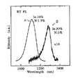
図1はGaAs/GaInNAs/GaAs構造のPL特性を示す図である。図1において、PL特性Aは、GaInNAsの組成が(In組成10%,N組成1.5%)の場合であり、また、PL特性Bは、GaInNAsの組成が(In組成30%,N組成1%)の場合である。図1から、Aの方が、Bに比べて、N組成が大きいにも関わらずPL強度は強くなっていることがわかる。このことから、N組成が同程度の場合、In組成が小さい方がPL強度は強く、結晶性が良好であることがわかる。これは混晶半導体のミシビリティーギャップと相関があると考えられる。
【0013】
【発明が解決しようとする課題】
上述した従来技術に対し、大きいN組成の混晶を得るために、特開平07−263744号には、III族原子とN以外のV族原子とからなる第1単原子層とIII族原子とN原子とからなる第2単原子層とを規則的に積層した単原子超格子構造が提案されている。例えば、第1単原子層としてGaP単原子層を6層、第2単原子層としてGaN単原子層を2層、ある並べ方で8原子層積層し、これを単位格子とし、この単位格子をさらに規則的に積層して発光層とする技術が提案されている。この技術によれば、GaNP混晶と同じバンドギャップを有する積層超格子構造を得ることができ、従来成長が困難であった大きい窒素組成のGaNP等のNを含んだ混晶を得ることができるとしている。
【0014】
このように、特開平07−263744号の方法では、V族がNのみからなるIII族−窒素化合物単原子層を用いているので、N組成が大きく特定の組成の混晶,例えばN組成が12.5%,25%,37.5%,50%,62.5%,75%,87.5%の混晶を、構造上得ることが可能となる。
【0015】
しかしながら、特開平07−263744号の方法では、形成できない組成がある。例えば1%などの小さいN組成の混晶半導体を形成しようとする場合、窒素化合物以外のIII−V族化合物単原子層を99原子層とV族がNのみからなるIII族−窒素化合物単原子層を1原子層用いる必要があるが、窒素化合物以外のIII−V族化合物層が30nm程度連続して存在することになりバルクとしての特性が現われるので、この超格子積層構造は混晶とは見なせない。このように、特開平07−263744号の方法では、任意の組成の混晶半導体を形成することができないという問題があった。
【0016】
本発明は、V族元素としてNおよび少なくとも他の1種のV族元素と、複数のIII族元素とから構成されるIII−V族混晶半導体の積層構造において、Nの取り込まれ効率を向上させ、結晶性の良好な任意の組成の混晶半導体が容易に得られる半導体積層構造を提供することを目的としている。
【0017】
また、本発明は、V族元素としてNおよび少なくとも他の1種のV族元素と、複数のIII族元素とから構成されるIII−V族混晶半導体を有する半導体発光素子において、発光効率の高い半導体発光素子を提供することを目的としている。
【0018】
【課題を解決するための手段】
上記目的を達成するために、請求項1記載の発明は、V族元素としてNおよび少なくとも他の1種のV族元素と、複数のIII族元素とから構成されるIII−V族混晶半導体の積層構造において、積層構造は、III族元素とV族元素とからなる単原子層を有し、III族元素としてInを含み、Inの組成比が異なる複数種の単原子層を規則的に積層して超格子積層構造として構成されていることを特徴としている。
【0019】
また、請求項2記載の発明は、請求項1記載の半導体積層構造において、上記III−V族混晶半導体は、GaxIn1−xNyAs1−y(0<x<1,0<y<1)であり、超格子積層構造は、In組成が小さいかもしくはInを含まないGax1In1−x1Ny1As1−y1(0<x1≦1,0<y1<1)からなる第1の単原子層と、In組成が大きいかもしくはGaを含まないGax2In1−x2Ny2As1−y2(0≦x2<1,0<y2<1)からなる第2の単原子層との少なくとも2種類の単原子層を有し、これらが規則的に積層されて構成されていることを特徴としている。
【0020】
また、請求項3記載の発明は、請求項1記載の半導体積層構造において、上記III−V族混晶半導体は、(AlxGa1-x)yIn1-yNzP1-z(0≦x≦1,0≦y≦1,0<z<1)であり、超格子積層構造は、In組成が小さいかもしくはInを含まない(AlxGa1-x)y1In1-y1Nz1P1-z1(0≦x≦1,0<y1≦1,0<z1<1)からなる第1の単原子層と、In組成が大きいかもしくはAlおよびGaを含まない(AlxGa1-x)y2In1-y2Nz2P1-z2(0≦x≦1,0≦y2<1,0<z2<1)からなる第2の単原子層との少なくとも2種類の単原子層を有し、これらが規則的に積層されて構成されていることを特徴としている。
【0021】
また、請求項4記載の発明は、請求項1乃至請求項3のいずれか一項に記載の半導体積層構造である超格子積層構造が発光層に用いられていることを特徴としている。
【0022】
【発明の実施の形態】
以下、本発明の実施形態を図面に基づいて説明する。本発明の半導体積層構造は、V族元素としてNおよび少なくとも他の1種のV族元素(例えば、As)と、複数のIII族元素(例えば、Ga,In)とから構成されるIII−V族混晶半導体の積層構造であって、III族元素とV族元素とからなる単原子層を有し、III族元素の組成比が異なる複数種の単原子層を規則的に積層して超格子積層構造SLとして構成され、これら複数種の単原子層の平均の組成の混晶半導体として構成されている。
【0023】
本発明では、超格子積層構造が、III−V族混晶半導体からなる複数種の単原子層により構成されていることから、これらの平均組成の混晶半導体と同じバンドギャップを持つことができるとともに、窒素Nの取り込まれやすい層を含んで構成できるので、平均組成の混晶半導体を単一で構成した場合に比べて、結晶性の良好な任意の組成の混晶半導体を容易に得ることができる。
【0024】
図2は本発明に係る半導体積層構造(III−V族化合物半導体の超格子積層構造)の構成例(第1の実施形態)を示す図である。図2を参照すると、この半導体積層構造は、上記III−V族混晶半導体が、GaxIn1−xNyAs1−y(0<x<1,0<y<1)であり、In組成が小さいかもしくはInを含まないGax1In1−x1Ny1As1−y1(0<x1≦1,0<y1<1)からなる第1の単原子層L1と、In組成が大きいかもしくはGaを含まないGax2In1−x2Ny2As1−y2(0≦x2<1,0<y2<1)からなる第2の単原子層L2との少なくとも2種類の単原子層を有し、これらが規則的に積層されて上記超格子積層構造SLが構成され、これらの平均の組成の混晶半導体として構成されている。
【0025】
図2の構成例では、超格子積層構造SLがIII−V族混晶半導体からなる少なくとも2種類の単原子層(例えば、L1,L2)により構成されていることにより、これらの平均組成の混晶半導体と同じバンドギャップをもつことができるとともに、In組成が小さいかもしくはInを含まない窒素Nの取り込まれやすい第1の単原子層L1を含んで構成されているので、III族元素がこれらの平均組成となるような単一組成で構成した場合に比べて、Nの取り込まれ効率が向上し、結晶性の良好なGaInNAsを容易に形成できる。
【0026】
また、図3は本発明に係る半導体積層構造(III−V族化合物半導体の超格子積層構造)の他の構成例(第2の実施形態)を示す図である。図3を参照すると、この半導体積層構造は、上記III−V族混晶半導体が、(AlxGa1-x)yIn1-yNzP1-z(0≦x≦1,0≦y≦1,0<z<1)であり、In組成が小さいかもしくはInを含まない(AlxGa1-x)y1In1-y1Nz1P1-z1(0≦x≦1,0<y1≦1,0<z1<1)からなる第1の単原子層M1と、In組成が大きいかもしくはAlおよびGaを含まない(AlxGa1-x)y2In1-y2Nz2P1-z2(0≦x≦1,0≦y2<1,0<z2<1)からなる第2の単原子層M2との少なくとも2種類の単原子層を有し、これらが規則的に積層されて上記超格子積層構造SLが構成されている。
【0027】
図3の構成例においても、超格子積層構造SLがIII−V族混晶半導体からなる少なくとも2種類の単原子層(例えば、M1,M2)により構成されていることにより、これらの平均組成の混晶半導体と同じバンドギャップをもつことができるとともに、In組成が小さいかもしくはInを含まない窒素Nの取り込まれやすい第1の単原子層M1を含んで構成されているので、III族元素がこれらの平均組成となるような単一組成で構成した場合に比べて、Nの取り込まれ効率が向上し、結晶性の良好な(Al)GaInNPを容易に形成できる。
【0028】
また、本発明の上記のような半導体積層構造(例えば、図2あるいは図3の半導体積層構造),すなわち、超格子積層構造は、半導体発光素子の発光層に用いることができる。
【0029】
このような半導体発光素子では、発光層である超格子積層構造が、III−V族混晶半導体からなる複数種の単原子層により構成されていることから、これらの平均組成の混晶半導体と同じバンドギャップをもつことができるとともに、窒素Nの取り込まれやすい層を含んで構成できるので、平均組成の混晶半導体を単一で構成した場合に比べてNの取り込まれ効率が向上し、結晶性の良好な混晶半導体が容易に得られ、発光効率の高い半導体発光素子を形成できる。
【0030】
【実施例】
以下、本発明の実施例について説明する。
【0031】
実施例1
実施例1では、図4に示すような半導体積層構造を作製した。なお、成長方法はMOCVD法で行なった。原料にはTMG(トリメチルガリウム),TMI(トリメチルインジウム),PH3(フォスフィン),AsH3(アルシン),そして窒素の原料にはDMHy(ジメチルヒドラジン)を用いた。キャリアガスにはH2を用いた。
【0032】
図4の超格子積層構造は、GaAs基板101上に、GaAsバッファ層102が形成され、GaAsバッファ層102上に、平均組成Ga0.72In0.28N0.014As0.986である量子井戸層103(膜厚が8nm)が形成され、量子井戸層103上に、GaAs保護層104(膜厚が0.2μm)が形成されたものとなっている。
【0033】
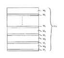
ここで、量子井戸層103は、Ga0.93In0.07N0.025As0.975の第1の単原子層L1を1層,Ga0.51In0.49N0.003As0.997の第2の単原子層L2を1層としたペアを、14ペア積層した超格子構造(1層の第1の単原子層L1と1層の第2の単原子層L2とを、それぞれ14層分、交互に積層した超格子構造)から構成されている。この際、2種類の単原子層L1,L2の成長条件は、III族の原料供給量比を相違させた他は同じとした。すなわち、2種類の単原子層L1,L2は、III族の原料供給量比に関して表1の組成に基づいた互いに異なる条件で成長させた。すなわち、第1の単原子層L1は、In組成を7%,N組成を2.5%として形成し、第2の単原子層L2は、In組成を49%,N組成を0.3%として形成した。このことから、Nの取り込まれがIn組成で大きく異なることがわかる。
【0034】
この超格子積層構造103は、平均組成Ga0.72In0.28N0.014As0.986の混晶とみなせる。GaInNAsでは、In組成が小さいほど窒素Nの取り込まれ効率が高く、N添加による結晶性の劣下率はIn組成の大きい材料より小さくなる。すなわち、同じ組成のGaInNAsでは、In組成が大きいほど結晶性が悪くなる。この実施例1では、In組成の平均組成は28%であるが、In組成28%のGaInNAsより窒素の取り込まれ効率が高いIn組成7%のGaInNAsの単原子層を含んで構成されているので、単一組成(平均組成28%)のGaInNAsのみで形成した場合に比べて、窒素組成を大きくすることができる。
【0035】
例えば、実施例1と同じ条件で、In組成28%のGaInNAsを成長させる場合、N組成は0.3%となる。これに対し、実施例1の超格子積層構造では、同じ成長条件で約5倍大きなN組成のGaInNAsを得ることができた。更にN添加による結晶性の劣下率が低い層にNを多く含ませたので、この試料のフォトルミネッセンス強度は均一組成(平均組成28%)で成長させたGaInNAsに比べて強かった。また、GaInNAs層のN組成は、AsH3に対するDMHyの供給量比を増やすほど、成長温度を下げるほど、成長速度を上げるほど、大きくなる傾向があった。また、各単原子層L1,L2は、混晶半導体により構成されているので、2元化合物を用いる場合に比べて超格子積層構造からなる任意の組成の混晶を得ることができる。
【0036】
実施例2
実施例2では、図5(a),(b)に示すような半導体発光素子(半導体レーザ素子)を作製した(ここで、図5(b)は図5(a)の半導体発光素子の量子井戸層の構成を示す図である)。なお、図5(a),(b)はGaAs基板上にGaInNAsによる長波長レーザを形成した例である。以下では、最も基本的な構造である絶縁膜ストライプ型レーザを例にして説明する。層構造としてはSCH−SQW(Separate Confinement Heterostructure Single Quantum Well)構造である。なお、成長方法はMOCVD法で行なった。原料にはTMG(トリメチルガリウム),TMI(トリメチルインジウム),PH3(フォスフィン),AsH3(アルシン),そして窒素の原料にはDMHy(ジメチルヒドラジン)を用いた。キャリアガスにはH2を用いた。
【0037】
すなわち、図5(a),(b)の半導体発光素子では、n−GaAs基板201上に、n−GaAsバッファ層202,n−Ga0.5In0.5P下部クラッド層203(膜厚が1.5μm),GaAs光ガイド層204(膜厚が100nm),平均組成Ga0.67In0.33N0.01As0.99である量子井戸層205(膜厚が8nm),GaAs光ガイド層206(膜厚が100nm),p−Ga0.5In0.5P上部クラッド層207(膜厚が1.5μm),p−GaAsコンタクト層208(膜厚が0.4μm)が順次に形成されている。また、この半導体発光素子では、その表面に、p側電極209が電流注入部となる部分を除去した絶縁膜210を介して形成されており、裏面にはn側電極211が形成されている。
【0038】
ここで、量子井戸層205は、InNAsの第1の単原子層L1を1層,GaNAsの第2の単原子層L2を2層としたペアを、9.5ペア積層した超格子構造から構成されている。この場合、各単原子層L1,L2はそれぞれ充分に厚さが薄いので、量子井戸層205はGaInNAsの混晶(平均組成がGa0.67In0.33N0.01As0.99の混晶)とみなせる。
【0039】
実施例1において説明したように、GaInNAsでは、In組成が小さいほど窒素の取り込まれ効率が高い。この実施例2の半導体発光素子の量子井戸層205は、窒素の取り込まれ効率が高いGaNAsの単原子層を含んで構成されているので、GaInNAsを単一組成で形成した場合に比べて、窒素組成は大きくなる。すなわち、超格子構造を用いた方が容易にGaInNAsを形成できる。更に、GaInNAsは、同一N組成の場合、In組成が小さいほど結晶性が良好となるので、実施例2の超格子構造により構成されたGa0.67In0.33N0.01As0.99は、均一組成で構成した場合に比べて、結晶性が良好になる。すなわち、N添加による結晶性の劣下率が低い層にNを多く含ませたので、この超格子積層構造による半導体の結晶性は良好になる。実際、実施例2の半導体発光素子を評価したところ、発振波長は1.3mであり、量子井戸層205が均一組成からなる素子に比べて、しきい値電流密度は低下した。
【0040】
実施例3
実施例3では、図6(a),(b)に示すような半導体発光素子(半導体レーザ素子)を作製した(ここで、図6(b)は図6(a)の半導体発光素子の量子井戸層を示す図である)。なお、図6(a),(b)はGaAs基板上にAlGaInNP系材料による短波長可視レーザを形成した例である。以下では、最も簡単な構造である絶縁膜ストライプ型レーザを例にして説明する。層構造としてはSCH−MQW(Separate Confinement Heterostructure Multiple Quantum Well)構造である。なお、成長方法はMOCVD法で行なった。原料にはTMA(トリメチルアルミニウム),TMG(トリメチルガリウム),TMI(トリメチルインジウム),AsH3(アルシン),PH3(フォスフィン)そして窒素の原料にはDMHy(ジメチルヒドラジン)を用いた。キャリアガスにはH2を用いた。
【0041】
すなわち、図6(a),(b)の半導体発光素子では、n−GaAs基板301上に、n−GaAsバッファ層302,n−(Al0.7Ga0.3)0.5In0.5P下部クラッド層303(膜厚が1.0μm),(Al0.5Ga0.5)0.5In0.5P下部光ガイド層304(膜厚が50nm),3層のGa0.65In0.35N0.005P0.995井戸層305(膜厚が7nm,引っ張り歪約1%)と2層の(Al0.5Ga0.5)0.5In0.5Pバリア層306(膜厚が8nm),(Al0.5Ga0.5)0.5In0.5P上部光ガイド層307(膜厚が50nm),p−(Al0.7Ga0.3)0.5In0.5P上部クラッド層308(膜厚が1.0μm),p−Ga0.5In0.5Pキャップ層309(膜厚が0.1μm),p−GaAsコンタクト層310(膜厚が0.4μm)が順次に形成されている。また、この半導体発光素子では、その表面に、p側電極311が電流注入部となる部分を除去した絶縁膜312を介して形成されており、裏面にはn側電極313が形成されている。
【0042】
ここで、量子井戸層305は、InNPの第1の原子層L1を1層、GaNPの第2の原子層L2を2層としたペアを、8.5ペア積層した超格子構造から構成されている。この場合、各原子層L1,L2はそれぞれ充分に厚さが薄いので、量子井戸層305は、GaInNPの混晶(平均組成がGa0.65In0.35N0.005P0.995の混晶)とみなせる。
【0043】
GaInNPでは、In組成が小さいほど窒素の取り込まれ効率が高い。この実施例3の半導体発光素子の量子井戸層305は、窒素の取り込まれ効率が高いGaNPの単原子層を含んで構成されているので、GaInNPを単一組成のみで形成した場合に比べて、窒素組成は大きくなる。すなわち、超格子構造を用いた方が容易にGaInNPを形成できる。更に、GaInNPは、同一N組成の場合、In組成が小さいほど結晶性が良好となるので、実施例3の超格子構造により構成されたGa0.65In0.35N0.005P0.995は、均一組成で構成した場合に比べて、結晶性が良好になる。実際、実施例3の半導体発光素子を評価したところ、量子井戸層305が均一組成からなる素子に比べて、しきい値電流密度の低い可視レーザが得られた。
【0044】
上記各実施例では、超格子積層構造における各原子組成や積層構成を限定したが、もちろん、これらに、他の組成や他の構成を用いることもできる。すなわち、V族元素としてNと他のV族元素を含み、III族元素として複数種のIII族元素を含んだ半導体材料であれば、同様の効果を得ることができる。また、本発明の半導体発光素子は、光通信用半導体レーザ,光書き込み用半導体レーザとして用いることができ、また、これ以外にも発光ダイオード、赤外光用フォトダイオードとして用いることもできる。
【0045】
【発明の効果】
以上に説明したように、請求項1記載の発明によれば、V族元素としてNおよび少なくとも他の1種のV族元素と、複数のIII族元素とから構成されるIII−V族混晶半導体の積層構造において、前記積層構造は、III族元素とV族元素とからなる単原子層を有し、III族元素としてInを含み、Inの組成比が異なる複数種の単原子層を規則的に積層して超格子積層構造として構成されているので、複数種の単原子層の平均組成の混晶半導体と同じバンドギャップを持つことができるとともに、窒素の取り込まれやすい層を含んで構成できることから、平均組成の混晶半導体を単一で構成した場合に比べて結晶性の良好な任意の組成の混晶半導体を容易に得ることができる。
【0046】
また、請求項2,請求項3記載の発明によれば、超格子積層構造が、In組成が小さいかもしくはInを含まない窒素の取り込まれやすい第1の単原子層を含んで構成されているので、III族元素がこれらの平均組成となるような単一組成で構成した場合に比べて、Nの取り込まれ効率が向上し、結晶性の良好なGaInNAs,結晶性の良好な(Al)GaInNPを容易に形成できる。
【0047】
また、請求項4記載の発明によれば、請求項1乃至請求項3のいずれか一項に記載の半導体積層構造である超格子積層構造が発光層に用いられており、超格子積層構造はIII−V族混晶半導体からなる複数種類の単原子層により構成されていることから、これらの平均組成の混晶半導体と同じバンドギャップを持つことができるとともに、窒素の取り込まれやすい層を含んで構成できるので平均組成の混晶半導体を単一で構成した場合に比べてNの取り込まれ効率が向上し、結晶性の良好な混晶半導体が容易に得られ、発光効率の高い発光素子を提供できる。
【図面の簡単な説明】
【図1】GaAs/GaInNAs/GaAs構造のPL特性を示す図である。
【図2】本発明に係る半導体積層構造(III−V族化合物半導体の超格子積層構造)の構成例(第1の実施形態)を示す図である。
【図3】本発明に係る半導体積層構造(III−V族化合物半導体の超格子積層構造)の他の構成例(第2の実施形態)を示す図である。
【図4】実施例1の半導体積層構造を示す図である。
【図5】実施例2の半導体発光素子を示す図である。
【図6】実施例3の半導体発光素子を示す図である。
【符号の説明】
L1,M1 第1の単原子層
L2,M2 第2の単原子層
101 GaAs基板
102 GaAsバッファ層
103 Ga0.72In0.28N0.014As0.986量子井戸層
104 GaAs保護層
201 n−GaAs基板
202 n−GaAsバッファ層
203 n−Ga0.5In0.5P下部クラッド層
204 GaAs光ガイド層
205 Ga0.67In0.33N0.01As0.99量子井戸層
206 GaAs光ガイド層
207 p−Ga0.5In0.5P上部クラッド層
208 p−GaAsコンタクト層
209 p側電極
210 絶縁膜
211 n側電極
301 n−GaAs基板
302 n−GaAsバッファ層
303 n−(Al0.7Ga0.3)0.5In0.5P下部クラッド層
304 (Al0.5Ga0.5)0.5In0.5P下部光ガイド層
305 3層のGa0.65In0.35N0.005P0.995井戸層
306 2層の(Al0.5Ga0.5)0.5In0.5Pバリア層
307 (Al0.5Ga0.5)0.5In0.5P上部光ガイド層
308 p−(Al0.7Ga0.3)0.5In0.5P上部クラッド層
309 p−Ga0.5In0.5Pキャップ層
310 p−GaAsコンタクト層
311 p側電極
312 絶縁膜
313 n側電極[0001]
TECHNICAL FIELD OF THE INVENTION
The present invention relates to a semiconductor laminated structure and a semiconductor light emitting device used for an optical device such as a semiconductor laser for optical communication, a semiconductor laser for optical writing, a light emitting diode, and a photodiode for infrared light.
[0002]
[Prior art]
Optical communication systems using optical fibers are currently mainly used in trunk systems, but are expected to be used in subscriber systems including homes in the future. To achieve this, it is necessary to reduce the size and cost of the system, and it is necessary to realize a system that does not require a Peltier element for temperature control. For this reason, there is a demand for a semiconductor laser device having a high characteristic temperature with a small change in characteristics due to a low threshold value operation and a temperature change.
[0003]
As a material intended to realize such an element, JP-A-6-37355 discloses a GaInNAs-based material which is a III-V mixed crystal semiconductor containing N and another group V element on a GaAs substrate. It has been proposed to form it. By adding N to GaInAs having a larger lattice constant than GaAs, the lattice constant can be lattice-matched to GaAs, and the bandgap energy is reduced to 1.3 μm, 1 μm. It is said to be a material capable of emitting light in the 0.5 μm band. Here, as a growth method of the GaInNAs-based material, a low pressure MOCVD (metal organic chemical deposition) method using active nitrogen is used.
[0004]
In the document “Jpn. J. Appl. Phys. Vol. 35 (1996) pp. 1273-1275”, the band lineup is calculated by Kondo et al. In this document, the band discontinuity of the conduction band is increased by using AlGaAs for the cladding layer in the GaAs lattice matching system. For this reason, it is expected that a high characteristic temperature semiconductor laser can be realized. The growth method of the GaAs lattice-matched system includes a gas source MBE (molecular) using active nitrogen.
beam epitaxy) method.
[0005]
In addition, the document “Electronics Letters, 1997, Vol. 33, pp. 1386-187” actually reports 1.3 μm band laser oscillation using a GaInNAs-based material. Here, the GaInNAs-based material is formed by an MOCVD method using DMHy (dimethylhydrazine) as a nitrogen source.
[0006]
In the above-described conventional technique, a mixed crystal semiconductor GaInNAs layer containing N in a group V element is grown by simultaneously supplying a Ga source, an In source, an N source, and an As source and having the same composition in the thickness direction. Is made by growing a mixed crystal. However, such mixed crystal semiconductors containing N in the V group can obtain only a few% of mixed crystals from the termination material. That is, the crystallinity of these GaInNAs tends to deteriorate as the N composition increases. On the other hand, in GaInNAs, increasing the In composition has the effect of reducing the band gap energy. For this reason, the N composition for obtaining oscillation at a certain wavelength (for example, 1.3 μm) may be smaller as the In composition is larger. Therefore, in the document “Jpn. J. Appl. Phys., Vol. 35 (1996) pp. 1273-1275”, GaInNAs having as good a crystallinity as possible are used for the quantum well active layer. 30%) of GaInNAs. The N composition is only 0.5%, and the oscillation wavelength is about 1.2 μm. For use in communications, the laser wavelength must be 1.3 μm and the N composition must be about 1%. The N composition of 1% is described in the document “Electronics Letters, 1997, Vol. 33, pp. 1386-1387 ", which is 1/3 of the N composition of GaInNAs having a small In composition (10%) of 3%, which is small.
[0007]
However, in practice, most mixed crystal semiconductors containing N in the group V element are in an immiscible region, and crystal growth is very difficult. A crystal having a slight nitrogen composition can be grown by MOCVD (metal organic chemical vapor deposition) or MBE (molecular beam epitaxy) having a high degree of non-equilibrium. As the number of constituent elements increases, the mixed crystal semiconductor becomes more immiscible. Further, even with the same mixed crystal, a mixed crystal having an intermediate composition has higher immiscibility. In other words, binary compounds are most likely to grow. The same can be said for a mixed crystal semiconductor containing N in a group V element.
[0008]
Thus, GaNAs is easier to grow than GaInNAs. Further, among GaInNAs, a material close to GaNAs is easier to grow. The following table (Table 1) shows the N composition of GaInNAs with the In composition changed on a GaAs substrate.
[0009]
[Table 1]
In Table 1, the N composition is a result obtained by SIMS analysis (secondary ion mass spectrometry). The growth was performed by MOCVD. The raw materials are TMG (trimethyl gallium), TMI (trimethyl indium), AsH3(Arsine) and DMHy (dimethylhydrazine) as a raw material for nitrogen. H for carrier gas2Was used. The growth temperature is 630 ° C. Then, only the supply amount of the TMI, which is the In raw material, was changed.
[0011]
Table 1 shows that the N concentration decreases as the In composition increases. Thus, in order to obtain a specific wavelength, the N composition can be reduced by increasing the In composition of GaInNAs. However, in the conventional growth method, when the In composition of GaInNAs is increased, the efficiency of N capture is increased. Was found to be reduced. Furthermore, it has been found that the crystallinity of GaInNAs tends to deteriorate as the N composition increases, and this tendency increases as the In composition increases.
[0012]
FIG. 1 is a diagram showing PL characteristics of a GaAs / GaInNAs / GaAs structure. In FIG. 1, the PL characteristic A is the case where the composition of GaInNAs is (10% In composition, 1.5% N composition), and the PL characteristic B is the case where the composition of GaInNAs is (30% In composition, N composition). 1%). From FIG. 1, it can be seen that the PL intensity is higher in A than in B despite the large N composition. From this, it can be seen that when the N composition is about the same, the smaller the In composition, the stronger the PL strength and the better the crystallinity. This is considered to have a correlation with the miscibility gap of the mixed crystal semiconductor.
[0013]
[Problems to be solved by the invention]
In order to obtain a mixed crystal having a large N composition with respect to the prior art described above, JP-A-07-263744 discloses a first monoatomic layer comprising a group III atom and a group V atom other than N and a group III atom. A monoatomic superlattice structure in which a second monoatomic layer composed of N atoms is regularly stacked has been proposed. For example, six GaP monolayers as the first monolayer, two GaN monolayers as the second monolayer, and eight atomic layers in a certain arrangement are stacked to form a unit lattice. A technique has been proposed in which light emitting layers are regularly laminated. According to this technique, it is possible to obtain a stacked superlattice structure having the same band gap as that of the GaNP mixed crystal, and to obtain a mixed crystal containing N such as GaNP having a large nitrogen composition, which has conventionally been difficult to grow. And
[0014]
As described above, in the method disclosed in JP-A-07-263744, a group III-nitrogen compound monoatomic layer in which the group V is composed of only N is used. 12.5%, 25%, 37.5%, 50%, 62.5%, 75%, and 87.5% of mixed crystals can be structurally obtained.
[0015]
However, there are some compositions that cannot be formed by the method of JP-A-07-263744. For example, when a mixed crystal semiconductor having a small N composition such as 1% is to be formed, a group III-V compound monoatomic layer other than a nitrogen compound is composed of a 99 atomic layer and a group III-nitrogen compound monoatomic group in which the group V includes only N. It is necessary to use one atomic layer, but since a group III-V compound layer other than a nitrogen compound is present continuously for about 30 nm and the characteristics as a bulk appear, this superlattice laminated structure is not a mixed crystal. Can't be considered. As described above, the method disclosed in JP-A-07-263744 has a problem that a mixed crystal semiconductor having an arbitrary composition cannot be formed.
[0016]
The present invention improves the incorporation efficiency of N in a stacked structure of a group III-V mixed crystal semiconductor composed of N as a group V element and at least one other group V element and a plurality of group III elements. Accordingly, it is an object of the present invention to provide a semiconductor laminated structure in which a mixed crystal semiconductor having an arbitrary composition having good crystallinity can be easily obtained.
[0017]
Further, the present invention provides a semiconductor light emitting device having a group III-V mixed crystal semiconductor composed of N as a group V element and at least one other group V element and a plurality of group III elements. It is intended to provide a high semiconductor light emitting device.
[0018]
[Means for Solving the Problems]
In order to achieve the above object, an invention according to
[0019]
According to a second aspect of the present invention, in the semiconductor multilayer structure of the first aspect, the III-V mixed crystal semiconductor is GaxIn1-xNyAs1-y(0 <x <1, 0 <y <1), and the superlattice laminated structure has a small In composition or Ga containing no In.x1In1-x1Ny1As1-y1A first monoatomic layer composed of (0 <x1 ≦ 1, 0 <y1 <1) and Ga having a large In composition or containing no Gax2In1-x2Ny2As1-y2(0 ≦ x2 <1, 0 <y2 <1) and a second monoatomic layer composed of at least two kinds of monoatomic layers, which are regularly laminated. I have.
[0020]
According to a third aspect of the present invention, in the semiconductor multilayer structure of the first aspect, the III-V mixed crystal semiconductor is (AlxGa1-x)yIn1-yNzP1-z(0 ≦ x ≦ 1, 0 ≦ y ≦ 1, 0 <z <1), and the superlattice laminated structure has a small In composition or does not contain In (AlxGa1-x)y1In1-y1Nz1P1-z1(0 ≦ x ≦ 1, 0 <y1 ≦ 1, 0 <z1 <1) and a first monoatomic layer having a large In composition orAl and Ga(AlxGa1-x)y2In1-y2Nz2P1-z2(0 ≦ x ≦ 1, 0 ≦ y2 <1, 0 <z2 <1) and at least two types of monoatomic layers, which are regularly laminated. It is characterized by having.
[0021]
The invention according to claim 4 is characterized in that the superlattice laminated structure which is the semiconductor laminated structure according to any one of
[0022]
BEST MODE FOR CARRYING OUT THE INVENTION
Hereinafter, embodiments of the present invention will be described with reference to the drawings. The semiconductor laminated structure according to the present invention has a III-V structure composed of N as a group V element and at least one other group V element (eg, As) and a plurality of group III elements (eg, Ga, In). A stacked structure of a group-C mixed crystal semiconductor, which has a monoatomic layer composed of a group III element and a group V element, and is formed by regularly laminating a plurality of types of monoatomic layers having different composition ratios of group III elements. It is configured as a lattice laminated structure SL, and is configured as a mixed crystal semiconductor having an average composition of these plural types of monoatomic layers.
[0023]
In the present invention, since the superlattice laminated structure is composed of a plurality of types of monoatomic layers made of a group III-V mixed crystal semiconductor, it can have the same band gap as a mixed crystal semiconductor having an average composition thereof. In addition, since it can be configured to include a layer in which nitrogen N is easily taken in, it is easy to obtain a mixed crystal semiconductor having an arbitrary composition with good crystallinity as compared with a case where a single mixed crystal semiconductor having an average composition is formed. Can be.
[0024]
FIG. 2 is a diagram showing a configuration example (first embodiment) of a semiconductor multilayer structure (superlattice multilayer structure of a III-V compound semiconductor) according to the present invention. Referring to FIG. 2, the semiconductor laminated structure is such that the III-V mixed crystal semiconductor is GaxIn1-xNyAs1-y(0 <x <1, 0 <y <1) and Ga having a small In composition or containing no Inx1In1-x1Ny1As1-y1First monoatomic layer L composed of (0 <x1 ≦ 1, 0 <y1 <1)1And Ga having a large In composition or containing no Gax2In1-x2Ny2As1-y2Second monoatomic layer L composed of (0 ≦ x2 <1, 0 <y2 <1)2The superlattice laminated structure SL is formed by regularly laminating at least two types of monoatomic layers, and is formed as a mixed crystal semiconductor having an average composition thereof.
[0025]
In the configuration example of FIG. 2, the superlattice stacked structure SL has at least two types of monoatomic layers (for example, L1, L2), The first monoatomic layer can have the same band gap as the mixed crystal semiconductors having these average compositions, and has a small In composition or is apt to take in nitrogen N containing no In. L1As compared with the case where the group III element has a single composition such that the group III element has the average composition, the efficiency of N incorporation is improved and GaInNAs having good crystallinity can be easily produced. Can be formed.
[0026]
FIG. 3 is a diagram showing another configuration example (second embodiment) of the semiconductor multilayer structure (superlattice multilayer structure of III-V compound semiconductor) according to the present invention. Referring to FIG. 3, in this semiconductor laminated structure, the III-V mixed crystal semiconductor is (AlxGa1-x)yIn1-yNzP1-z(0 ≦ x ≦ 1, 0 ≦ y ≦ 1, 0 <z <1), and the In composition is small or does not contain In (AlxGa1-x)y1In1-y1Nz1P1-z1(0 ≦ x ≦ 1, 0 <y1 ≦ 1, 0 <z1 <1) First monoatomic layer M1And the In composition is large orAl and Ga(AlxGa1-x)y2In1-y2Nz2P1-z2(0 ≦ x ≦ 1, 0 ≦ y2 <1, 0 <z2 <1) Second monoatomic layer MTwoAnd at least two types of monoatomic layers, which are regularly laminated to form the superlattice laminated structure SL.
[0027]
Also in the configuration example of FIG. 3, the superlattice stacked structure SL has at least two types of monoatomic layers (for example, M1, M2), The first monoatomic layer having the same band gap as the mixed crystal semiconductors having these average compositions and having a small In composition or easily containing nitrogen N containing no In. M1, The efficiency of N incorporation is improved and the crystallinity of the (Al) GaInNP is improved, as compared with the case where the group III element has a single composition having the average composition thereof. Can be easily formed.
[0028]
Further, the above-described semiconductor multilayer structure of the present invention (for example, the semiconductor multilayer structure of FIG. 2 or FIG. 3), that is, the superlattice multilayer structure can be used for a light emitting layer of a semiconductor light emitting device.
[0029]
In such a semiconductor light emitting device, the superlattice laminated structure as the light emitting layer is composed of a plurality of types of monoatomic layers made of a group III-V mixed crystal semiconductor. Since it can have the same band gap and can be configured to include a layer in which nitrogen N is easily incorporated, the efficiency of N incorporation is improved as compared with the case where a single crystal mixed crystal having an average composition is formed, and A mixed crystal semiconductor having good properties can be easily obtained, and a semiconductor light emitting device with high luminous efficiency can be formed.
[0030]
【Example】
Hereinafter, examples of the present invention will be described.
[0031]
Example 1
In Example 1, a semiconductor multilayer structure as shown in FIG. 4 was manufactured. The growth was performed by MOCVD. The raw materials are TMG (trimethyl gallium), TMI (trimethyl indium), PH3(Phosphine), AsH3(Arsine) and DMHy (dimethylhydrazine) as a raw material for nitrogen. H for carrier gas2Was used.
[0032]
4 has a
[0033]
Here, the
[0034]
The superlattice laminated
[0035]
For example, when growing GaInNAs having an In composition of 28% under the same conditions as in Example 1, the N composition is 0.3%. On the other hand, in the superlattice laminated structure of Example 1, GaInNAs having an N composition approximately five times larger than that of N was obtained under the same growth conditions. Further, since N was added to a layer having a low inferiority in crystallinity due to the addition of N, the photoluminescence intensity of this sample was stronger than that of GaInNAs grown with a uniform composition (average composition: 28%). The N composition of the GaInNAs layer is AsH3As the ratio of DMHy to DMHy increased, the growth temperature decreased, and the growth rate increased, the ratio tended to increase. In addition, each monoatomic layer L1, L2Is composed of a mixed crystal semiconductor, so that a mixed crystal having an arbitrary composition having a superlattice laminated structure can be obtained as compared with the case where a binary compound is used.
[0036]
Example 2
In Example 2, a semiconductor light emitting device (semiconductor laser device) as shown in FIGS. 5A and 5B was manufactured (here, FIG. 5B shows the quantum of the semiconductor light emitting device of FIG. 5A). It is a figure showing composition of a well layer). FIGS. 5A and 5B are examples in which a long wavelength laser made of GaInNAs is formed on a GaAs substrate. In the following, an example of an insulating film stripe type laser having the most basic structure will be described. The layer structure is an SCH-SQW (Separate Definition Heterostructure Single Quantum Well) structure. The growth was performed by MOCVD. The raw materials are TMG (trimethyl gallium), TMI (trimethyl indium), PH3(Phosphine), AsH3(Arsine) and DMHy (dimethylhydrazine) as a raw material for nitrogen. H for carrier gas2Was used.
[0037]
That is, in the semiconductor light emitting device of FIGS. 5A and 5B, the n-
[0038]
Here, the
[0039]
As described in the first embodiment, in GaInNAs, the smaller the In composition is, the higher the nitrogen incorporation efficiency is. Since the
[0040]
Example 3
In Example 3, a semiconductor light emitting device (semiconductor laser device) as shown in FIGS. 6A and 6B was manufactured (here, FIG. 6B shows the quantum of the semiconductor light emitting device of FIG. 6A). It is a figure which shows a well layer). 6A and 6B are examples in which a short-wavelength visible laser made of an AlGaInNP-based material is formed on a GaAs substrate. In the following, an example of an insulating film stripe type laser having the simplest structure will be described. The layer structure is an SCH-MQW (Separate Definition Heterostructure Multiple Quantum Well) structure. The growth was performed by MOCVD. Raw materials include TMA (trimethylaluminum), TMG (trimethylgallium), TMI (trimethylindium), AsH3(Arsine), PH3(Phosphine) and DMHy (dimethylhydrazine) was used as a raw material for nitrogen. H for carrier gas2Was used.
[0041]
That is, in the semiconductor light emitting device of FIGS. 6A and 6B, an n-
[0042]
Here, the
[0043]
In GaInNP, the smaller the In composition is, the higher the efficiency of taking in nitrogen is. Since the
[0044]
In each of the above embodiments, the atomic composition and the laminated structure in the superlattice laminated structure are limited, but of course, other compositions and other structures can be used. That is, a similar effect can be obtained as long as the semiconductor material contains N as a group V element and another group V element, and contains a plurality of group III elements as a group III element. Further, the semiconductor light emitting device of the present invention can be used as a semiconductor laser for optical communication and a semiconductor laser for optical writing, and can also be used as a light emitting diode and a photodiode for infrared light.
[0045]
【The invention's effect】
As described above, according to the invention of
[0046]
According to the second and third aspects of the present invention, the superlattice laminated structure is configured to include the first monoatomic layer having a small In composition or containing no In and containing nitrogen easily. Therefore, as compared with the case where the group III element has a single composition having the above average composition, the efficiency of N incorporation is improved, and GaInNAs having good crystallinity and (Al) GaInNP having good crystallinity are obtained. Can be easily formed.
[0047]
According to a fourth aspect of the present invention, the superlattice laminated structure, which is the semiconductor laminated structure according to any one of the first to third aspects, is used for a light emitting layer. Since it is composed of a plurality of types of monoatomic layers made of a group III-V mixed crystal semiconductor, it can have the same band gap as a mixed crystal semiconductor having an average composition thereof, and includes a layer in which nitrogen is easily taken in. Therefore, compared to the case where a single crystal of the average composition is used, the efficiency of N incorporation is improved, and a mixed crystal semiconductor with good crystallinity can be easily obtained. Can be provided.
[Brief description of the drawings]
FIG. 1 is a diagram showing PL characteristics of a GaAs / GaInNAs / GaAs structure.
FIG. 2 is a diagram illustrating a configuration example (first embodiment) of a semiconductor multilayer structure (superlattice multilayer structure of a group III-V compound semiconductor) according to the present invention.
FIG. 3 is a diagram showing another configuration example (second embodiment) of the semiconductor multilayer structure (superlattice multilayer structure of a group III-V compound semiconductor) according to the present invention.
FIG. 4 is a diagram illustrating a semiconductor multilayer structure according to the first embodiment.
FIG. 5 is a diagram showing a semiconductor light emitting device of Example 2.
FIG. 6 is a diagram showing a semiconductor light emitting device of Example 3.
[Explanation of symbols]
L1, M1 First monolayer
L2, M2 Second monolayer
101 GaAs substrate
102 GaAs buffer layer
103 Ga0.72In0.28N0.014As0.986Quantum well layer
104 GaAs protective layer
201 n-GaAs substrate
202 n-GaAs buffer layer
203 n-Ga0.5In0.5P lower cladding layer
204 GaAs light guide layer
205 Ga0.67In0.33N0.01As0.99Quantum well layer
206 GaAs light guide layer
207 p-Ga0.5In0.5P upper cladding layer
208 p-GaAs contact layer
209 p-side electrode
210 insulating film
211 n-side electrode
301 n-GaAs substrate
302 n-GaAs buffer layer
303 n- (Al0.7Ga0.3)0.5In0.5P lower cladding layer
304 (Al0.5Ga0.5)0.5In0.5P lower light guide layer
305 Three layers of Ga0.65In0.35N0.005P0.995Well layer
306 Two layers of (Al0.5Ga0.5)0.5In0.5P barrier layer
307 (Al0.5Ga0.5)0.5In0.5P upper light guide layer
308 p- (Al0.7Ga0.3)0.5In0.5P upper cladding layer
309 p-Ga0.5In0.5P cap layer
310 p-GaAs contact layer
311 p-side electrode
312 Insulating film
313 n-side electrode
Claims (4)
Translated fromJapanesePriority Applications (2)
| Application Number | Priority Date | Filing Date | Title |
|---|---|---|---|
| JP35007197AJP3547037B2 (en) | 1997-12-04 | 1997-12-04 | Semiconductor laminated structure and semiconductor light emitting device |
| US09/204,292US6281518B1 (en) | 1997-12-04 | 1998-12-03 | Layered III-V semiconductor structures and light emitting devices including the structures |
Applications Claiming Priority (1)
| Application Number | Priority Date | Filing Date | Title |
|---|---|---|---|
| JP35007197AJP3547037B2 (en) | 1997-12-04 | 1997-12-04 | Semiconductor laminated structure and semiconductor light emitting device |
Publications (2)
| Publication Number | Publication Date |
|---|---|
| JPH11168242A JPH11168242A (en) | 1999-06-22 |
| JP3547037B2true JP3547037B2 (en) | 2004-07-28 |
Family
ID=18408039
Family Applications (1)
| Application Number | Title | Priority Date | Filing Date |
|---|---|---|---|
| JP35007197AExpired - Fee RelatedJP3547037B2 (en) | 1997-12-04 | 1997-12-04 | Semiconductor laminated structure and semiconductor light emitting device |
Country Status (2)
| Country | Link |
|---|---|
| US (1) | US6281518B1 (en) |
| JP (1) | JP3547037B2 (en) |
Families Citing this family (66)
| Publication number | Priority date | Publication date | Assignee | Title |
|---|---|---|---|---|
| US6563851B1 (en)* | 1998-04-13 | 2003-05-13 | Ricoh Company, Ltd. | Laser diode having an active layer containing N and operable in a 0.6 μm wavelength band |
| US6884291B1 (en)* | 1998-04-13 | 2005-04-26 | Ricoh Company, Ltd. | Laser diode having an active layer containing N and operable in a 0.6 μm wavelength band |
| US7384479B2 (en)* | 1998-04-13 | 2008-06-10 | Ricoh Company, Ltd. | Laser diode having an active layer containing N and operable in a 0.6 μm wavelength |
| US6674785B2 (en)* | 2000-09-21 | 2004-01-06 | Ricoh Company, Ltd. | Vertical-cavity, surface-emission type laser diode and fabrication process thereof |
| US6803604B2 (en)* | 2001-03-13 | 2004-10-12 | Ricoh Company, Ltd. | Semiconductor optical modulator, an optical amplifier and an integrated semiconductor light-emitting device |
| JP4537658B2 (en) | 2002-02-22 | 2010-09-01 | 株式会社リコー | Surface emitting laser element, surface emitting laser array using the surface emitting laser element, electrophotographic system, surface emitting laser module, optical communication system, optical interconnection system, and surface emitting laser element manufacturing method |
| US6927412B2 (en)* | 2002-11-21 | 2005-08-09 | Ricoh Company, Ltd. | Semiconductor light emitter |
| US7227174B2 (en)* | 2003-06-26 | 2007-06-05 | Rj Mears, Llc | Semiconductor device including a superlattice and adjacent semiconductor layer with doped regions defining a semiconductor junction |
| US7531829B2 (en)* | 2003-06-26 | 2009-05-12 | Mears Technologies, Inc. | Semiconductor device including regions of band-engineered semiconductor superlattice to reduce device-on resistance |
| US7531828B2 (en)* | 2003-06-26 | 2009-05-12 | Mears Technologies, Inc. | Semiconductor device including a strained superlattice between at least one pair of spaced apart stress regions |
| US7586165B2 (en)* | 2003-06-26 | 2009-09-08 | Mears Technologies, Inc. | Microelectromechanical systems (MEMS) device including a superlattice |
| US7446002B2 (en)* | 2003-06-26 | 2008-11-04 | Mears Technologies, Inc. | Method for making a semiconductor device comprising a superlattice dielectric interface layer |
| US20070010040A1 (en)* | 2003-06-26 | 2007-01-11 | Rj Mears, Llc | Method for Making a Semiconductor Device Including a Strained Superlattice Layer Above a Stress Layer |
| US7045377B2 (en)* | 2003-06-26 | 2006-05-16 | Rj Mears, Llc | Method for making a semiconductor device including a superlattice and adjacent semiconductor layer with doped regions defining a semiconductor junction |
| US7153763B2 (en) | 2003-06-26 | 2006-12-26 | Rj Mears, Llc | Method for making a semiconductor device including band-engineered superlattice using intermediate annealing |
| US20060292765A1 (en)* | 2003-06-26 | 2006-12-28 | Rj Mears, Llc | Method for Making a FINFET Including a Superlattice |
| US20070020860A1 (en)* | 2003-06-26 | 2007-01-25 | Rj Mears, Llc | Method for Making Semiconductor Device Including a Strained Superlattice and Overlying Stress Layer and Related Methods |
| US20040262594A1 (en)* | 2003-06-26 | 2004-12-30 | Rj Mears, Llc | Semiconductor structures having improved conductivity effective mass and methods for fabricating same |
| US7535041B2 (en)* | 2003-06-26 | 2009-05-19 | Mears Technologies, Inc. | Method for making a semiconductor device including regions of band-engineered semiconductor superlattice to reduce device-on resistance |
| US20070020833A1 (en)* | 2003-06-26 | 2007-01-25 | Rj Mears, Llc | Method for Making a Semiconductor Device Including a Channel with a Non-Semiconductor Layer Monolayer |
| US7612366B2 (en)* | 2003-06-26 | 2009-11-03 | Mears Technologies, Inc. | Semiconductor device including a strained superlattice layer above a stress layer |
| US7531850B2 (en)* | 2003-06-26 | 2009-05-12 | Mears Technologies, Inc. | Semiconductor device including a memory cell with a negative differential resistance (NDR) device |
| US20070015344A1 (en)* | 2003-06-26 | 2007-01-18 | Rj Mears, Llc | Method for Making a Semiconductor Device Including a Strained Superlattice Between at Least One Pair of Spaced Apart Stress Regions |
| US20060243964A1 (en)* | 2003-06-26 | 2006-11-02 | Rj Mears, Llc | Method for making a semiconductor device having a semiconductor-on-insulator configuration and a superlattice |
| US7598515B2 (en)* | 2003-06-26 | 2009-10-06 | Mears Technologies, Inc. | Semiconductor device including a strained superlattice and overlying stress layer and related methods |
| US7659539B2 (en) | 2003-06-26 | 2010-02-09 | Mears Technologies, Inc. | Semiconductor device including a floating gate memory cell with a superlattice channel |
| US7229902B2 (en)* | 2003-06-26 | 2007-06-12 | Rj Mears, Llc | Method for making a semiconductor device including a superlattice with regions defining a semiconductor junction |
| US20060289049A1 (en)* | 2003-06-26 | 2006-12-28 | Rj Mears, Llc | Semiconductor Device Having a Semiconductor-on-Insulator (SOI) Configuration and Including a Superlattice on a Thin Semiconductor Layer |
| US20050282330A1 (en)* | 2003-06-26 | 2005-12-22 | Rj Mears, Llc | Method for making a semiconductor device including a superlattice having at least one group of substantially undoped layers |
| US20060231857A1 (en)* | 2003-06-26 | 2006-10-19 | Rj Mears, Llc | Method for making a semiconductor device including a memory cell with a negative differential resistance (ndr) device |
| US7514328B2 (en)* | 2003-06-26 | 2009-04-07 | Mears Technologies, Inc. | Method for making a semiconductor device including shallow trench isolation (STI) regions with a superlattice therebetween |
| US20070063186A1 (en)* | 2003-06-26 | 2007-03-22 | Rj Mears, Llc | Method for making a semiconductor device including a front side strained superlattice layer and a back side stress layer |
| US7045813B2 (en)* | 2003-06-26 | 2006-05-16 | Rj Mears, Llc | Semiconductor device including a superlattice with regions defining a semiconductor junction |
| US6897472B2 (en)* | 2003-06-26 | 2005-05-24 | Rj Mears, Llc | Semiconductor device including MOSFET having band-engineered superlattice |
| US20040266116A1 (en)* | 2003-06-26 | 2004-12-30 | Rj Mears, Llc | Methods of fabricating semiconductor structures having improved conductivity effective mass |
| US7586116B2 (en)* | 2003-06-26 | 2009-09-08 | Mears Technologies, Inc. | Semiconductor device having a semiconductor-on-insulator configuration and a superlattice |
| US6878576B1 (en) | 2003-06-26 | 2005-04-12 | Rj Mears, Llc | Method for making semiconductor device including band-engineered superlattice |
| US7491587B2 (en)* | 2003-06-26 | 2009-02-17 | Mears Technologies, Inc. | Method for making a semiconductor device having a semiconductor-on-insulator (SOI) configuration and including a superlattice on a thin semiconductor layer |
| US20060011905A1 (en)* | 2003-06-26 | 2006-01-19 | Rj Mears, Llc | Semiconductor device comprising a superlattice dielectric interface layer |
| US20050279991A1 (en)* | 2003-06-26 | 2005-12-22 | Rj Mears, Llc | Semiconductor device including a superlattice having at least one group of substantially undoped layers |
| JP2007521648A (en)* | 2003-06-26 | 2007-08-02 | アール.ジェイ. メアーズ エルエルシー | Semiconductor device having MOSFET with band design superlattice |
| US20060267130A1 (en)* | 2003-06-26 | 2006-11-30 | Rj Mears, Llc | Semiconductor Device Including Shallow Trench Isolation (STI) Regions with a Superlattice Therebetween |
| US20060220118A1 (en)* | 2003-06-26 | 2006-10-05 | Rj Mears, Llc | Semiconductor device including a dopant blocking superlattice |
| US7202494B2 (en)* | 2003-06-26 | 2007-04-10 | Rj Mears, Llc | FINFET including a superlattice |
| US7064037B2 (en)* | 2004-01-12 | 2006-06-20 | Chartered Semiconductor Manufacturing Ltd. | Silicon-germanium virtual substrate and method of fabricating the same |
| US7709728B2 (en)* | 2004-11-29 | 2010-05-04 | The Regents Of The University Of California | Multiband semiconductor compositions for photovoltaic devices |
| US7517702B2 (en)* | 2005-12-22 | 2009-04-14 | Mears Technologies, Inc. | Method for making an electronic device including a poled superlattice having a net electrical dipole moment |
| WO2007076008A2 (en)* | 2005-12-22 | 2007-07-05 | Mears Technologies, Inc | Electronic device including a poled superlattice having a net electrical dipole moment and associated methods |
| US7693204B2 (en) | 2006-02-03 | 2010-04-06 | Ricoh Company, Ltd. | Surface-emitting laser device and surface-emitting laser array including same |
| WO2007098138A2 (en)* | 2006-02-21 | 2007-08-30 | Mears Technologies, Inc. | Semiconductor device comprising a lattice matching layer and associated methods |
| US7781827B2 (en) | 2007-01-24 | 2010-08-24 | Mears Technologies, Inc. | Semiconductor device with a vertical MOSFET including a superlattice and related methods |
| US7928425B2 (en)* | 2007-01-25 | 2011-04-19 | Mears Technologies, Inc. | Semiconductor device including a metal-to-semiconductor superlattice interface layer and related methods |
| US7863066B2 (en)* | 2007-02-16 | 2011-01-04 | Mears Technologies, Inc. | Method for making a multiple-wavelength opto-electronic device including a superlattice |
| US7880161B2 (en)* | 2007-02-16 | 2011-02-01 | Mears Technologies, Inc. | Multiple-wavelength opto-electronic device including a superlattice |
| US7812339B2 (en)* | 2007-04-23 | 2010-10-12 | Mears Technologies, Inc. | Method for making a semiconductor device including shallow trench isolation (STI) regions with maskless superlattice deposition following STI formation and related structures |
| US7723719B2 (en)* | 2007-12-14 | 2010-05-25 | Palo Alto Research Center Incorporated | Light emitting devices with inhomogeneous quantum well active regions |
| KR20100084843A (en)* | 2009-01-19 | 2010-07-28 | 삼성전자주식회사 | Multijunction solar cell |
| JP2014123712A (en) | 2012-11-26 | 2014-07-03 | Ricoh Co Ltd | Method of manufacturing solar cell |
| CN105900241B (en) | 2013-11-22 | 2020-07-24 | 阿托梅拉公司 | Semiconductor device including superlattice depletion layer stack and related methods |
| WO2015077595A1 (en) | 2013-11-22 | 2015-05-28 | Mears Technologies, Inc. | Vertical semiconductor devices including superlattice punch through stop layer and related methods |
| WO2015191561A1 (en) | 2014-06-09 | 2015-12-17 | Mears Technologies, Inc. | Semiconductor devices with enhanced deterministic doping and related methods |
| US9722046B2 (en) | 2014-11-25 | 2017-08-01 | Atomera Incorporated | Semiconductor device including a superlattice and replacement metal gate structure and related methods |
| US9941359B2 (en) | 2015-05-15 | 2018-04-10 | Atomera Incorporated | Semiconductor devices with superlattice and punch-through stop (PTS) layers at different depths and related methods |
| US9721790B2 (en) | 2015-06-02 | 2017-08-01 | Atomera Incorporated | Method for making enhanced semiconductor structures in single wafer processing chamber with desired uniformity control |
| US9558939B1 (en) | 2016-01-15 | 2017-01-31 | Atomera Incorporated | Methods for making a semiconductor device including atomic layer structures using N2O as an oxygen source |
| US10879420B2 (en) | 2018-07-09 | 2020-12-29 | University Of Iowa Research Foundation | Cascaded superlattice LED system |
Family Cites Families (5)
| Publication number | Priority date | Publication date | Assignee | Title |
|---|---|---|---|---|
| JP3445653B2 (en)* | 1994-03-23 | 2003-09-08 | 士郎 酒井 | Light emitting element |
| JPH08195522A (en)* | 1994-11-16 | 1996-07-30 | Hitachi Ltd | Semiconductor laser |
| US5825796A (en)* | 1996-09-25 | 1998-10-20 | Picolight Incorporated | Extended wavelength strained layer lasers having strain compensated layers |
| JPH10173294A (en)* | 1996-10-07 | 1998-06-26 | Canon Inc | Compound semiconductor multilayer mirror containing nitrogen and surface light emitting device using the same |
| US5978398A (en)* | 1997-07-31 | 1999-11-02 | Motorola, Inc. | Long wavelength vertical cavity surface emitting laser |
- 1997
- 1997-12-04JPJP35007197Apatent/JP3547037B2/ennot_activeExpired - Fee Related
- 1998
- 1998-12-03USUS09/204,292patent/US6281518B1/ennot_activeExpired - Lifetime
Also Published As
| Publication number | Publication date |
|---|---|
| JPH11168242A (en) | 1999-06-22 |
| US6281518B1 (en) | 2001-08-28 |
Similar Documents
| Publication | Publication Date | Title |
|---|---|---|
| JP3547037B2 (en) | Semiconductor laminated structure and semiconductor light emitting device | |
| JP3683669B2 (en) | Semiconductor light emitting device | |
| US7166874B2 (en) | Nitride semiconductor with active layer of quantum well structure with indium-containing nitride semiconductor | |
| US9166102B2 (en) | Group III nitride semiconductor light-emitting device including a superlatice layer | |
| JP3719613B2 (en) | Semiconductor light emitting device | |
| US6198112B1 (en) | III-V compound semiconductor luminescent device | |
| US20040065887A1 (en) | Light emitting devices with layered III -V semiconductor structures, and modules and systems for computer, network and optical communication, using such devices | |
| KR20100064383A (en) | (al, in, ga, b)n device structures on a patterned substrate | |
| WO2000017972A1 (en) | Process for producing nitride semiconductor device | |
| US20150115220A1 (en) | (Al, In, Ga, B)N DEVICE STRUCTURES ON A PATTERNED SUBSTRATE | |
| JP4097232B2 (en) | Semiconductor laser element | |
| US6348698B1 (en) | Layered semiconductor structures and light emitting devices including the structure | |
| JP4097238B2 (en) | Semiconductor laminated structure and semiconductor light emitting device | |
| JP3654331B2 (en) | Semiconductor manufacturing method and semiconductor light emitting device | |
| JP2000004068A (en) | Semiconductor light emitting device | |
| US20080265275A1 (en) | Semiconductor device and manufacturing method therefor | |
| JP4002323B2 (en) | Method for producing compound semiconductor | |
| US5246878A (en) | Capping layer preventing deleterious effects of As--P exchange | |
| JP2000091710A (en) | Semiconductor laminated structure and semiconductor light emitting device | |
| Agahi et al. | Tensile‐strained barrier GaAsP/GaAs single quantum‐well lasers | |
| JP2967719B2 (en) | Semiconductor crystal growth method and semiconductor device | |
| KR20240148838A (en) | Photonic materials | |
| JPH10256670A (en) | Compound semiconductor device | |
| Heller et al. | Low-threshold room-temperature continuous-wave InP quantum dot coupled to InGaP quantum well heterorstructure lasers grown by metalorganic chemical vapor deposition | |
| JP2010153564A (en) | Semiconductor laser element and manufacturing method thereof |
Legal Events
| Date | Code | Title | Description |
|---|---|---|---|
| A977 | Report on retrieval | Free format text:JAPANESE INTERMEDIATE CODE: A971007 Effective date:20031219 | |
| A131 | Notification of reasons for refusal | Free format text:JAPANESE INTERMEDIATE CODE: A131 Effective date:20040107 | |
| A521 | Request for written amendment filed | Free format text:JAPANESE INTERMEDIATE CODE: A523 Effective date:20040303 | |
| TRDD | Decision of grant or rejection written | ||
| A01 | Written decision to grant a patent or to grant a registration (utility model) | Free format text:JAPANESE INTERMEDIATE CODE: A01 Effective date:20040407 | |
| A61 | First payment of annual fees (during grant procedure) | Free format text:JAPANESE INTERMEDIATE CODE: A61 Effective date:20040408 | |
| R150 | Certificate of patent or registration of utility model | Free format text:JAPANESE INTERMEDIATE CODE: R150 | |
| FPAY | Renewal fee payment (event date is renewal date of database) | Free format text:PAYMENT UNTIL: 20080423 Year of fee payment:4 | |
| FPAY | Renewal fee payment (event date is renewal date of database) | Free format text:PAYMENT UNTIL: 20090423 Year of fee payment:5 | |
| FPAY | Renewal fee payment (event date is renewal date of database) | Free format text:PAYMENT UNTIL: 20100423 Year of fee payment:6 | |
| FPAY | Renewal fee payment (event date is renewal date of database) | Free format text:PAYMENT UNTIL: 20100423 Year of fee payment:6 | |
| FPAY | Renewal fee payment (event date is renewal date of database) | Free format text:PAYMENT UNTIL: 20110423 Year of fee payment:7 | |
| FPAY | Renewal fee payment (event date is renewal date of database) | Free format text:PAYMENT UNTIL: 20120423 Year of fee payment:8 | |
| FPAY | Renewal fee payment (event date is renewal date of database) | Free format text:PAYMENT UNTIL: 20130423 Year of fee payment:9 | |
| FPAY | Renewal fee payment (event date is renewal date of database) | Free format text:PAYMENT UNTIL: 20140423 Year of fee payment:10 | |
| LAPS | Cancellation because of no payment of annual fees |